modern clocking strategies - date-conference.com are assumed to know about sequential logic design...
TRANSCRIPT

Modern Clocking Strategies
Organisers:
Jordi Cortadella, Universitat Politecnica de CatalunyaLuciano Lavagno, Politecnico di TorinoAlex Yakovlev, University of Newcastle
Speakers:
Koen van Eijk, SynopsysAlex Yakovlev, University of NewcastleDavid M. Zar, BlendicsJordi Cortadella, Universitat Politecnica de Catalunya

1 Overview
Clock network design and timing analysis are among the most challenging tasks in integratedcircuit design. The former also exhibits the broadest range of very different solutions, rang-ing from classical zero-skew clocking, to multiple independent clock islands, each operatingat a different Dynamic Voltage and Frequency Scaling (DVFS) point, and to clocks thatdynamically adapt to the timing characteristics of the underlying logic. Of course, everyclocking strategy must be supported by a corresponding verification method on the statictiming analysis side. This can be particularly tricky when the clocks become less and lesssynchronous, due to power management methods or to techniques that improve robustnesswith respect to variability.
This tutorial is aimed at covering the full range of synthesis and verification tasks forthe clocks, starting from basic definitions and techniques, and then gradually expanding thehorizon.
Each talk will be offered by a leading industrial or academic expert, and will enabledesigners to choose the best synchronization technique for the problem at hand.
Attendees are assumed to know about sequential logic design and basic single-phase zero-skew clocking. They will gain knowledge about the following topics: (1) clock synthesis andtiming analysis, especially in conjunction with power management techniques such as clockgating, power gating and DVFS; (2) reliability analysis in the presence of meta-stability forclock domain crossing; (3) asynchronous synchronization techniques; (4) advanced adaptiveclocking strategies, where the clock latency or period adapts to the operating conditions ofthe logic.
2 Lectures
The tutorial will be organized in four lectures, each one covering different aspects of clocksynthesis and timing. Next, an abstract of each lecture is presented.
Clock Synthesis and Chip Variability (Koen van Eijk, Synopsys)
One of the main challenges for clock synthesis is dealing with chip variability. With thedecreasing dimensions and lower voltages used by new generations of CMOS technology,global and local variations are becoming more and more important. Clock synthesis needsto take variation tolerance into account, to mitigate the impact of these variations.
Mainstream methods for clock tree synthesis typically work by building an initial clockstructure in a bottom-up fashion, and then optimizing this structure to improve insertiondelay, skew, power and area. These methods can consider variation tolerance by includingtechniques such as multi-corner optimization, common path sharing and balancing of celland wire delays. For the global distribution of high-frequency clocks, a different approachis commonly used, which is based on using clock structures that are robust by construction,such as H-trees and clock meshes. Multisource clock synthesis combines these approaches, to
1

support a range of clock structures that provide good trade-offs between robustness, powerand area.
In this lecture we will first explain the basics of clock synthesis and timing closure forsynchronous circuits, and then describe in more detail techniques and design styles for high-performance, variation tolerant clock structures.
Asynchronous timing (Alex Yakovlev, University of Newcastle)
Can we coordinate circuits in time without clock? The answer is yes, if we use asynchronouscircuits. These circuits, also called self-timed circuits, do not rely on a global clock signaland operate using local synchronization mechanisms such as handshakes. This makes themvery different from widely adopted synchronous circuits and promises many benefits, suchas inherent resilience to process, voltage, temperature and aging variations, average ratherthan worst-case operation in time and power domains, and better modularity and composi-tionality. For example, asynchronous timing enables robust operation at near-threshold orsub-threshold voltages (NTV and STV), where the optimum point for energy-per-operationlies for many types of logic and memory. This capability allows asynchronous timing to fitideally for systems powered by energy harvesting, e.g. Internet-of-Things nodes.
Despite these benefits, asynchronous timing is not yet widely adopted by industry, mainlybecause of the difficulties of integrating it into the standard EDA tool flows.
In this lecture we will provide a brief overview of the state-of-the-art of asynchronoustiming. We will focus on its two main design paradigms, bundled data and delay-insensitivecircuits, and compare their gains and penalties. We will demonstrate existing asynchronoustool support for both paradigms.
We will also highlight recent success stories, in particular, industrially adopted designflow for little digital hardware components asynchronous circuits providing flexible timingfor analog/mixed-signal circuits such a power converters and AD converters.
Finally, we will discuss how these tools can be used for the design of elastic data-flowpipelines, as well as fully self-timed SRAMs, which allows creating systems where processorsand memory can seamlessly operate at NVT/SVT. We will conclude by posing future researchand development challenges that are currently on the agenda of the asynchronous community.
Metastability and Clock Domain Crossing (David M. Zar, Blendics)
Multiple-clock system-on-chip (SOC) designs require synchronization when transferring sig-nals and data among clock domains and when receiving asynchronous inputs. Such synchro-nizations are often susceptible to metastability effects that may propagate into the receivingcircuit and may cause malfunctions. To mitigate the nondeterministic effects associated withmetastability, latches and flip-flops are often used to synchronize the data. Common struc-tures for this purpose include pipelined flip-flops and FIFOs. There is, however, a probabilitythat these circuits will not resolve from a metastable state within the allowed time. Theprobabilities are becoming a concern as technology nodes get smaller and as the intrinsic
2

parameters of the devices become increasingly variable and problematic; scaling does nothelp us, anymore!
For multiple-clock SOC designs it is important to understand how synchronizer circuitsmay fail, and to be able to design reliability as measured by a particular allowable proba-bility of failure, or level of failures in time (FIT). This lecture will present some commonsynchronization structures, where they may be used and how to evaluate their reliabilityfor both an individual synchronizer and for a system with many synchronizers. Parametersthat govern synchronizer reliability are contained in the process transistor-model and in theapplication of the synchronizer. These two different sources of parameters often involve twodifferent designers and who may work in two different companies. Methods to unite thesesources will be discussed.
Some of the latest research in this area will be presented along with models, examples ofgood synchronizer circuits and a discussion of why data flip-flops make terrible synchronizingdevices.
Advanced Clocking (Jordi Cortadella, Universitat Politecnica deCatalunya)
Clock frequency is one of the most important parameters in system design and typically is apre-defined target before synthesis. The time uncertainties in nanoelectronics circuits due toprocess, voltage, temperature and aging (PVTA) variations demand safe guardband marginsthat result in conservative clock frequencies. These margins imply a high cost in energy andperformance.
In the last few years, several techniques for adaptive clocking have emerged with the aimof dynamically adapting the frequency of the clock to the dynamic variations (VTA) of thesystem. These techniques may contribute to reduce energy consumption up to 40%. Amongall the sources of variations, the most challenging problem is the safe adaptation to voltagedroops. This lecture will review some of the most recent advances in adaptive clocking.
Few companies have proposed different schemes based on anticipating voltage droops andquickly adapting the clock frequency to the delays of the system while the droop is active.Various approaches around this idea will be presented and discussed.
Techniques based on resilient circuits proposed by ARM and Intel will be also covered.These techniques are based on pushing clock frequency to the limits in a way that timingerrors may be detected and corrected at runtime. These techniques require sophisticatedmechanisms for error detection/correction not always available in conventional systems.
Finally, a technique based on substituting the PLL by a ring oscillator will be presented.The design and power/performance benefits of this technique will be analyzed.
3

3 Biographies
Jordi Cortadella is Professor and Head of the Computer Science Department at the Uni-versitat Politcnica de Catalunya. He is a Fellow of the IEEE and member of the AcademiaEuropaea. He holds a M.S. and a Ph.D. degree in Computer Science (Universitat Politc-nica de Catalunya, 1985 and 1987). In 1988, he was a Visiting Scholar at the Universityof California, Berkeley. His research interests include formal methods and computer-aideddesign of VLSI systems with special emphasis on asynchronous circuits, concurrent systemsand logic synthesis. He has co-authored numerous research papers and has been invited topresent tutorials at various conferences.
Prof. Cortadella has served on the technical committees of several international confer-ences in the field of Design Automation and Concurrent Systems and is associate editor ofthe IEEE Transactions on CAD of Integrated Circuits and Systems. He received best paperawards at DAC 2004, ASYNC 2004 and ACSD 2009. In 2003, he was the recipient of aDistinction for the Promotion of the University Research by the Generalitat de Catalunya.
Luciano Lavagno received his Ph.D. in electrical engineering and computer science fromthe University of California at Berkeley, CA, USA, in 1992. He has been the architect of thePOLIS project, developing a complete hardware/software co-design environment for control-dominated embedded systems, and an architect of the CtoSilicon high-level synthesis systemfrom Cadence Design Systems. He is a co-author of two books on asynchronous circuitdesign, of a book on hardware/software co-design of embedded systems, and has publishedover 200 journal and conference papers.
He is currently a full Professor with the Department of Electronics and Telecommunica-tion Engineering of Politecnico di Torino, Italy. He has been an Associate Editor of IEEETCAS and ACM TECS. His research interests include the synthesis of asynchronous and low-power circuits, the concurrent design of mixed hardware and software embedded systems,and the high-level synthesis of hardware modules from algorithmic specifications.
Koen van Eijk is a Scientist in the Design Group at Synopsys, Inc, where he works on clocktree synthesis. Prior to joining Synopsys in 2012, he was a Chief Technologist at MagmaDesign Automation, where he worked on placement, physical optimization, floorplanning,and hierarchical design implementation. Dr. van Eijk studied at the Electrical EngineeringDepartment of the Eindhoven University of Technology, from which he graduated with honorsin 1992 and obtained a Ph.D. degree in 1997, on the topic of equivalence checking for digitalcircuits.
Alex Yakovlev was a Dream Fellow of Engineering and Physical Sciences Research Council(EPSRC), United Kingdom, to investigate different aspects of energy-modulated computingduring 2012-2013.
He received D.Sc. from Newcastle University in 2006, and M.Sc. and Ph.D. from St.Petersburg Electrical Engineering Institute in 1979 and 1982 respectively, where he workedin the area of asynchronous and concurrent systems since 1980, and in the period between1982 and 1990 held positions of assistant and associate professor at the Computing Science
4

department. Since 1991 he has been at the Newcastle University, where he is a professorand head of the MicroSystems research group at the School of Electrical and ElectronicEngineering. His current interests and publications are in the field of modelling and designof asynchronous, concurrent, real-time and dependable systems on a chip. He has published8 edited and co-authored monographs and more than 300 papers in academic journals andconferences, and has managed over 30 research contracts. He is a Senior Member of theIEEE and Fellow of IET.
He has chaired program committees of several international conferences, including theIEEE Int. Symposium on Asynchronous Circuits and Systems (ASYNC), Petri nets (ICATPN),Applications of Concurrency to Systems Design (ACSD), and he has been Chairman of theSteering committee of the Conference on Application of Concurrency to System Design since2001. In April 2008 he was General Chair of the 14th ASYNC Symposium and 2nd Int. Sym-posium on Networks on Chip, 22nd PATMOS, and Tutorial Chair at Design Automationand Test in Europe (DATE) in 2009. He has served as a Steering committee member forASYNC, NOCS, ICATPN, PATMOS. He was recently an invited speaker at DDECS 2010,KTN event on Power Management in 2010, DATE 2011, DCIS 2014, where he spoke onAsynchronous Systems and Energy-Modulated Computing. He was a tutorial organiser andspeaker at DATE 2013, gave lectures and courses on asynchronous design at ARM, IMECand Dialog Seminconductor in 2015.
David M. Zar is a Co-Founder of Blendics where he is also a Senior Engineer workingon metastability-related tools and analysis. Along with several of the other Co-Founders ofBlendics, Mr. Zar came from Washington University in St. Louis where he was involved inasynchronous circuit design as well as metastability work on and off for over 19 years. Heis the principal developer of MetaACE, the first commercially available tool for the analysisof metastability in synchronizers. In addition, Mr. Zar has worked in the areas of medicaldevices, networking and cybersecurity for the past 25 years.
5

Clock Synthesis
and Chip Variability
Koen van Eijk
Synopsys

Modern Clocking Strategies: Clock Synthesis and Chip Variability
Koen van Eijk Synopsys
1. Clock Synthesis Fundamentals
2. Chip Variability and Timing Sign-Off
3. Variation Tolerant Clock Structures
4. Design Flow Aspects and Automation
Overview
Clock Synthesis and Chip Variability 1 DATE 2016

Setup timing check • The data must arrive at the
D input before the arrival of the next clock edge
Hold timing check • The data must remain valid
long enough after the arrival of the clock edge
Multiple clock domains, clock gating, latches, path exceptions, …
Synchronous Circuits
Clock Synthesis and Chip Variability 2 DATE 2016
CLK
combinational logic D Q
FF1
D Q
FF2
Setup timing check • The data must arrive at the
D input before the arrival of the next clock edge
Hold timing check • The data must remain valid
long enough after the arrival of the clock edge
Multiple clock domains, clock gating, latches, path exceptions, …
Synchronous Circuits
Clock Synthesis and Chip Variability 3 DATE 2016
CLK
combinational logic D Q
FF1
D Q
FF2
launching clock path
capturing clock path
data path

Clock Tree Synthesis
DATE 2016 Clock Synthesis and Chip Variability 4
• Clock tree synthesis creates the network that connects the system clock to the sequential elements of the chip
• Main goals
• Balance insertion delays
• Minimize clock area and power
• The later flow stages include clock optimization
Placement and optimization
Clock Tree Synthesis
Routing and optimization
Ide
al c
lock
s P
rop
agat
ed
clo
cks
• Skew: Difference in arrival times at clock inputs
• Global: Between the clock inputs of any two sequential elements in the same clock domain
• Local: Between two clock inputs that launch and capture a timing path
• Positive skew: Capture comes later than launch
• Negative skew: Capture comes earlier than launch
• Useful skew: Use skew to meet signal timing
• Create positive skew on timing-critical paths
• Accept negative skew on non-timing-critical paths
Clock Balancing
DATE 2016 Clock Synthesis and Chip Variability 5

• Use static timing analysis to check that all timing constraints are satisfied
• Determine the worst possible conditions for each type of timing check
• How to account for chip variability?
Timing Sign-Off
DATE 2016 Clock Synthesis and Chip Variability 6
Correctness Yield
Lifetime
Timing Closure Die Size Power
Process • Variation in critical dimensions
• Random dopant fluctuation
• Variation of the gate oxide thickness
Sources of Variation
DATE 2016 Clock Synthesis and Chip Variability 7
Reference: M. Wirnshofer, Variation-Aware Voltage Scaling for Digital CMOS Circuits, Springer Series in Advanced Microelectronics 41
Voltage • Offset in the voltage regulator
• Power noise (IR drop, di/dt noise)
Temperature • Ambient temperature changes
• Global variations and local fluctuations due to power dissipation
Aging • Hot carrier injection
• Bias temperature instability

• Main origin of random variability in conventional bulk transistors
• Responsible for ~60% of device-to-device VT variation at 45nm
• For SOI and 3D multi-gate transistors, the channel/body doping can be eliminated to mitigate RDF effects
• Still other sources of random variability
Example: Random Dopant Fluctuation
DATE 2016 Clock Synthesis and Chip Variability 8
Source: K. Kuhn et al., Managing Process Variation in Intel’s 45nm CMOS Technology, Intel Technology
Journal, Volume 12, Issue 2, 2008
P
N N
• Systematic versus random
• Systematic variations are deterministic in nature, can be attributed to layout or manufacturing equipment related effects, and generally show spatial correlation behavior
• Global versus local
• Global variations affect similar components on the same die in the same way
• Static versus dynamic
• Dynamic variation is time-dependent, with time constants ranging from small (power noise) to large (aging)
• Process variation is static
Classifying Variation
DATE 2016 Clock Synthesis and Chip Variability 9

• Multicorner analysis
• Model chip-to-chip variations
• Examples: Ambient temperature, metal dimensions
• Basic OCV modeling
• Model variations with min/max delays
• Examples: Power noise, temperature fluctuations
• Advanced and parametric OCV
• Model correlations to reduce pessimism
• Examples: Random dopant fluctuation, effective gate lengths
Modeling variation
DATE 2016 Clock Synthesis and Chip Variability 10
• Perform conservative checks by applying maximum and minimum delays • Example: Define min/max by -10%/+10% derating
Basic OCV Modeling
DATE 2016 Clock Synthesis and Chip Variability 11
CLK
combinational logic D Q
FF1
D Q
FF2
CLK
combinational logic D Q
FF1
D Q
FF2
max delay
min delay
Setup timing check Hold timing check

• It is pessimistic to assume both minimum and maximum delays for the common part
• CRPR removes this pessimism by only assuming maximum delays for the common part
Clock Reconvergence Pessimism Removal
DATE 2016 Clock Synthesis and Chip Variability 12
CLK
combinational logic D Q
FF1
D Q
FF2
max delay
min delay CLK
combinational logic D Q
FF1
D Q
FF2
• Advanced OCV
• Derate values as a function of logic depth (for random variations) and location (for systematic variations)
Advanced and Parametric OCV
DATE 2016 Clock Synthesis and Chip Variability 13
• Parametric OCV
• Computes arrival times, required times and slacks as statistical distributions

Creating Robust Clock Structures
DATE 2016 Clock Synthesis and Chip Variability 14
Synthesis algorithm
– Bottom-up tree construction using clustering, buffering, clock gate merging, splitting, sizing and relocation
Techniques for improving variation tolerance
–Multi-corner optimization
–Gate/wire delay balancing
– Common path sharing
Gate/Wire Delay Balancing
DATE 2016 Clock Synthesis and Chip Variability
15
Balancing with Cell Delay Only Balancing with Cell & Wire Delay
Corner Scaling Ratio For gate: 2:1
For Wire: 1:1.5
A B
A B
A GATE WIRE
4.0 4.0
B GATE WIRE
5.0 3.0
A GATE WIRE
4.0 4.0
B GATE WIRE
3.5 4.5
Corner 1
A GATE WIRE
2.0 6.0
B GATE WIRE
2.5 4.5
A GATE WIRE
2.0 6.0
B GATE WIRE
1.75 6.75
Corner 2

Common Path Sharing
DATE 2016 Clock Synthesis and Chip Variability 16
• Prefer late branching
Early branching Late branching
• Timing-aware clustering
Robust by Construction
DATE 2016 Clock Synthesis and Chip Variability 17
Global clock tree (H-tree)
– Structural balancing
– Strong repeaters and high layers to achieve low latency Less impact from OCV derating Less sensitive to variations
Clock mesh
–OCV tolerance
Clock subtrees
– Flexibility for fine-grain clock gating and useful skew

Trade-offs for Multisource CTS
DATE 2016 Clock Synthesis and Chip Variability 18
Regular CTS Multisource CTS
w/o mesh Multisource CTS
with mesh
Lower power
More robust against global and local variations
Lower latency
Fewer flow steps
Automation & easy exploration
1. Create mesh routes
• Non-default rule, shielding
2. Insert mesh drivers
• Placed in regular pattern
3. Hook up pins to mesh
• Restrict topology to avoid daisy chaining
4. Analyze and annotate delays
• Integrated circuit simulation
Mesh Creation
DATE 2016 Clock Synthesis and Chip Variability 19
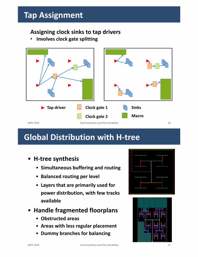
Tap Assignment
DATE 2016 Clock Synthesis and Chip Variability 20
Tap driver Clock gate 1
Clock gate 2
Sinks
Macro
Assigning clock sinks to tap drivers • Involves clock gate splitting
Global Distribution with H-tree
DATE 2016 Clock Synthesis and Chip Variability 21
• H-tree synthesis
• Simultaneous buffering and routing
• Balanced routing per level
• Layers that are primarily used for
power distribution, with few tracks
available
• Handle fragmented floorplans • Obstructed areas
• Areas with less regular placement
• Dummy branches for balancing

• Insert cells with tunable delays and tune the delay to minimize skew • Typically part of the global clock distribution
Post-Silicon Clock Tuning
DATE 2016 Clock Synthesis and Chip Variability 22
dynamic tuning static tuning
Source: B. Doyle et al., Clock distribution on a dual-core, multi-threaded Itanium/spl reg/ family
microprocessor. Integrated Circuit Design and Technology, 2005.
• Variation tolerant clock structures • Improving balancing and path sharing in bottom-up tree construction
• Global distribution with H-tree
• Clock mesh for very high performance designs
• Complete flow support for multisource CTS • Tap synthesis, mesh creation and analysis, global tree synthesis
Summary
DATE 2016 Clock Synthesis and Chip Variability 23
Correctness Yield
Lifetime
Timing Closure Die Size Power
Chip Variability
Asynchronous Timing
Alex Yakovlev
University of Newcastle

Modern Clocking Strategies:
Asynchronous Timing
Jordi Cortadella UPC, Barcelona
Alex Yakovlev
Newcastle University, UK
• Starting from Synchronous
• Completion Detection
• Handshaking
• Why going asynchronous?
• Towards near and sub-threshold
• GALS – Globally Asynchronous, Locally Synchronous
• Design Automation
Overview
1 Asynchronous timing
DATE 2016

Synchronous circuits
DATE 2016 Asynchronous timing 2
Synchronous circuit
DATE 2016 Asynchronous timing
Combinational Logic
Flip
Flo
ps
Flip
Flo
ps
PLL
3

1 2 1 1 2
Synchronous circuit
DATE 2016 Asynchronous timing
CL
Two competing paths: • Launching path • Capturing path
Launching path < Capturing path + Period
CLKtree + CL < CLKtree + Period
CL < Period (no clock skew)
2 PLL
4
Source-synchronous
DATE 2016 Asynchronous timing
CLK gen matched delay matched delay matched delay
• No global clock required
• More tolerance to PVT variations
• Period > longest combinational path
• Good for acyclic pipelines
Launching path
Capturing path
5

CLK gen
?
Source-synchronous with forks and joins
DATE 2016 Asynchronous timing
How to synchronize incoming events?
6
Completion detection
DATE 2016 Asynchronous timing 7
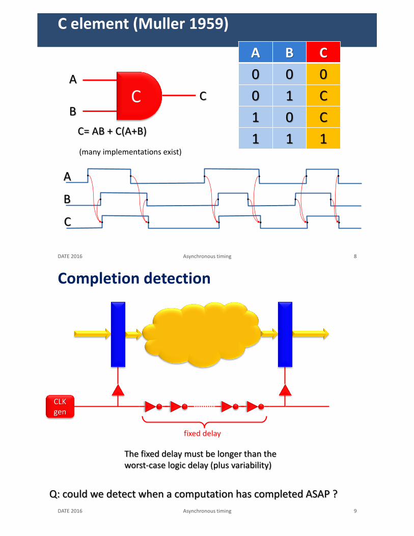
C element (Muller 1959)
DATE 2016 Asynchronous timing
C A
B C
A
B
C
A B C
0 0 0
0 1 C
1 0 C
1 1 1
8
C= AB + C(A+B)
(many implementations exist)
Completion detection
DATE 2016 Asynchronous timing
CLK gen
fixed delay
The fixed delay must be longer than the worst-case logic delay (plus variability)
Q: could we detect when a computation has completed ASAP ?
9

A 1 SP 0 SP 1 SP 1 SP
Delay-insensitive codes: Dual Rail
• Dual rail: every bit encoded with two signals
DATE 2016 Asynchronous timing
A.t A.f A
0 0 Spacer
0 1 0
1 0 1
1 1 Not used
A.t
A.f
10
Plus: • Systematic code • Easy to extract value • Easy to detect completion Minus: • More area • More power
DI codes (1-of-n and m-of-n)
• 1-of-4:
• 0001=> 00, 0010=>01, 0100=>10, 1000=>11
• 2-of-4:
• 1100, 1010, 1001, 0110, 0101, 0011 – total 6 combinations (cf. 2-bit dual-rail – 4 comb.)
• 3-of-6:
• 111000, 110100, …, 000111 – total 20 combinations (can encode 4 bits + 4 control tokens)
• 2-of-7:
• 1100000, 1010000, …, 0000011 – total 21 combinations (4 bits + 5 control tokens)
11 DATE 2016 Asynchronous timing

Dual-Rail AND gate
DATE 2016 Asynchronous timing
A B C
SP SP SP
0 - 0
- 0 0
SP 1 SP
1 SP SP
1 1 1
A
B C
A.t
A.f
B.t
B.f
C.t
C.f
12
Single rail data vs. dual rail
Some back-of-the-envelope estimations:
DATE 2016 Asynchronous timing
Single rail Dual Rail
Area 1 2
Delay 1 << 1
Static power 1 2
Dynamic power < 0.2 2
Dual rail: • Good for speed • Large area • High power consumption
13

Handshaking
DATE 2016 Asynchronous timing 14
Handshaking
DATE 2016 Asynchronous timing
CLK gen
unknown delay
Assume that the source module can provide data at any rate:
• When should the CLK generator send an event if the
internal delays of the circuit are unknown?
Solution: handshaking
15

Handshaking
DATE 2016 Asynchronous timing
I have data
I want data
Data
Request
Acknowledge
16
Asynchronous elastic pipeline
C
ReqIn ReqOut
AckIn AckOut
C C C
• David Muller’s pipeline (late 50’s) • Sutherland’s Micropipelines (Turing award, 1989)
DATE 2016 Asynchronous timing 17

Multiple inputs and outputs
DATE 2016 Asynchronous timing 18
Multiple inputs and outputs
DATE 2016 Asynchronous timing 19
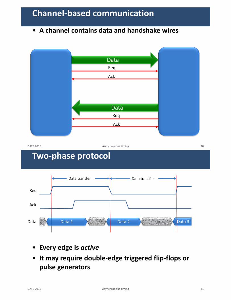
Channel-based communication
• A channel contains data and handshake wires
DATE 2016 Asynchronous timing
Data Req
Ack
20
Data Req
Ack
Two-phase protocol
• Every edge is active
• It may require double-edge triggered flip-flops or pulse generators
DATE 2016 Asynchronous timing
Data 1 Data 2 Data 3
Req
Ack
Data
Data transfer Data transfer
21
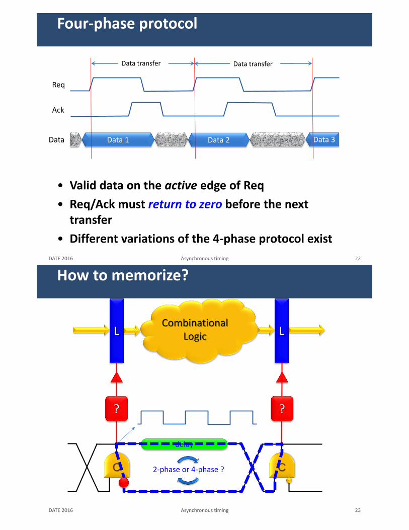
Four-phase protocol
• Valid data on the active edge of Req
• Req/Ack must return to zero before the next transfer
• Different variations of the 4-phase protocol exist
DATE 2016 Asynchronous timing
Data 1 Data 2 Data 3
Req
Ack
Data
Data transfer Data transfer
22
How to memorize?
DATE 2016 Asynchronous timing
Combinational Logic L L
delay
C C
? ?
2-phase or 4-phase ?
23

How to memorize?
DATE 2016 Asynchronous timing
Combinational Logic L L
delay
C C
Pulse generator
2-phase
24
How to memorize?
DATE 2016 Asynchronous timing
Combinational Logic L L
delay
C C 4-phase
25

Why going asynchronous?
DATE 2016 Asynchronous timing 26
Modularity
• Time-independent functional composability • Performance may be affected (but not functionality)
DATE 2016 Asynchronous timing 27
A B Data Req
Ack B’

Tracking variability
DATE 2016 Asynchronous timing 28
matched delay
Tracking variability
delay
best typ worst
Good correlation for:
• Process variability (systematic)
• Global voltage fluctuations
• Temperature
• Aging (partially)
DATE 2016 Asynchronous timing 29

Margins
Gate and wire delays (typ) P V T Aging PLL
Jitter Skew
Rigid Clocks:
Cycle period
Gate and wire delays (typ) P V T
Ag
ing
Elastic Clocks:
Skew
Cycle period
Margin reduction
Speed-up / Power savings
DATE 2016 Asynchronous timing 30
wasted time computation time
Rigid clock
computation time
Cycle period
Cycle period
Elastic clock
Clock elasticity
DATE 2016 Asynchronous timing 31
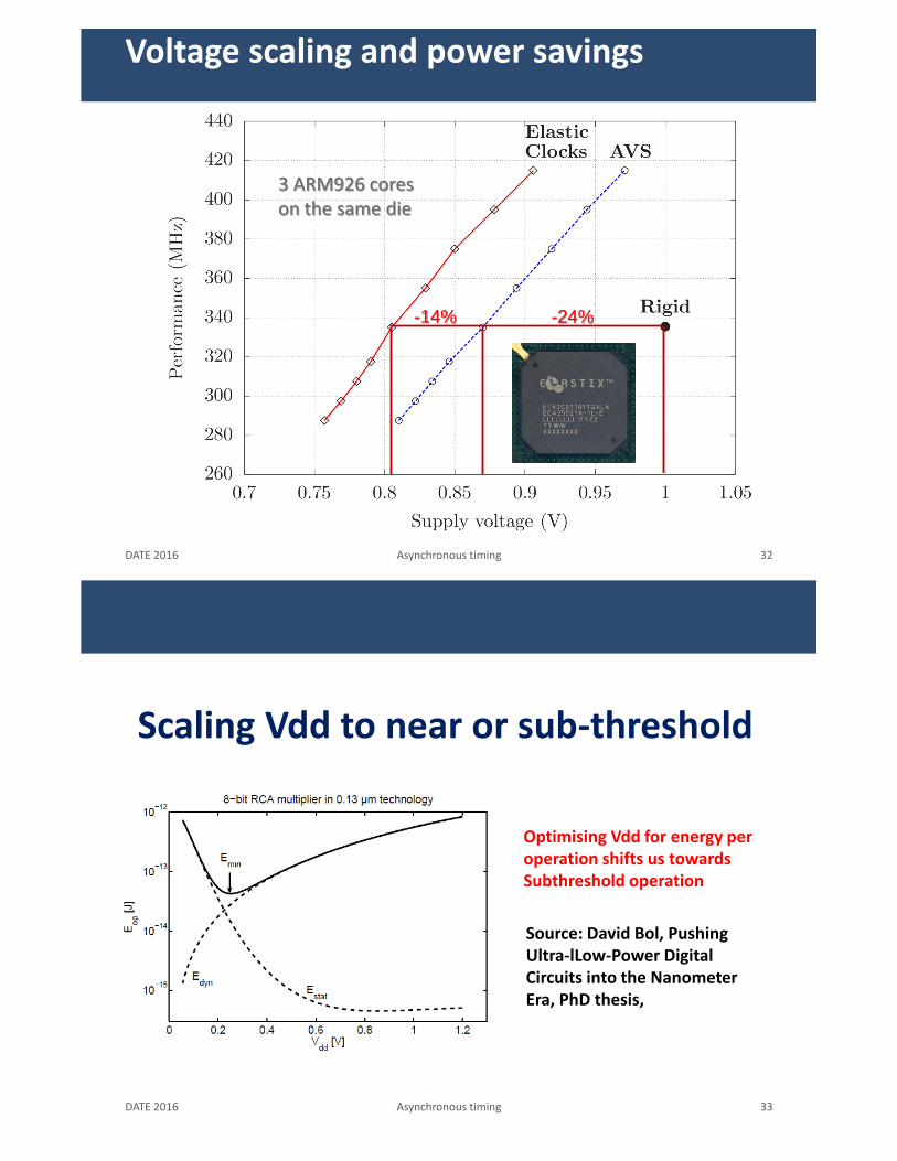
Voltage scaling and power savings
-24% -14%
3 ARM926 cores on the same die
DATE 2016 Asynchronous timing 32
Scaling Vdd to near or sub-threshold
DATE 2016 Asynchronous timing 33
Source: David Bol, Pushing Ultra-lLow-Power Digital Circuits into the Nanometer Era, PhD thesis,
Optimising Vdd for energy per operation shifts us towards Subthreshold operation

Relationship with timing variability
But we need to be more
timing robust!
Source of variability
analysis:
Yu Cao, Clark, L.T.,
2007
Technology node:
90nm
Optimising Vdd for energy per operation shifts us towards Subthreshold operation
34 DATE 2016 Asynchronous timing
Example: 8-bit Booth’s Multiplier
• Synchronous • Rigid 1GHz clock
• Frequency scaling
• Tuned for 1GHz, 500MHz and 250MHz
• Asynchronous, bundled data • Extra control logic and delay lines
• Asynchronous, dual-rail
• Double comb. logic and FF size (more leakage) • Extra completion detection and single-rail to dual-rail
converters • Double switching activity (spacer/code-word)
35 DATE 2016 Asynchronous timing

Benchmark Architectures
Adaptive frequency scaling Bundled data
Dual-rail
36 DATE 2016 Asynchronous timing
Multiplier: Power-speed scaling
37 DATE 2016 Asynchronous timing

Globally Asynchronous Locally Synchronous (GALS)
DATE 2016 Asynchronous timing 38
DATE 2016 Asynchronous timing 39
Clocking and interfaces: Towards GALS
Example from IHP Baseband processor design (Moonrake chip), GALAXY project
Synchronous
Asynchronous
GALS

Measurements of Moonrake Chip
GALS has shown:
much better EMI profile
improved power consumption and
reduced area!
Area (mm2)
Power Dissipation
(mW)
Spectral amplitude of Core VDD (dBm)
1st peak 2nd peak 3rd peak
SYNC TX 2.33
(43.2%)
258 -15 -32 -23
GALS TX 2.22
(41.0%) 237 -41 -48 -53
Difference +4.7% +8.2% 26dB 16dB 30dB
Amplitude of on-chip core VDD from SYNC TX
Amplitude of on-chip core VDD from GALS TX
Source: M. Krstic et al. Evaluation of GALS Methods in Scaled CMOS Technology: Moonrake Chip Experience, IJERTCS, 3(4), 2012
40 DATE 2016 Asynchronous timing
DATE 2016 Asynchronous timing 41
GALS: asynchronous wrapper
Request-Acknowledge Window
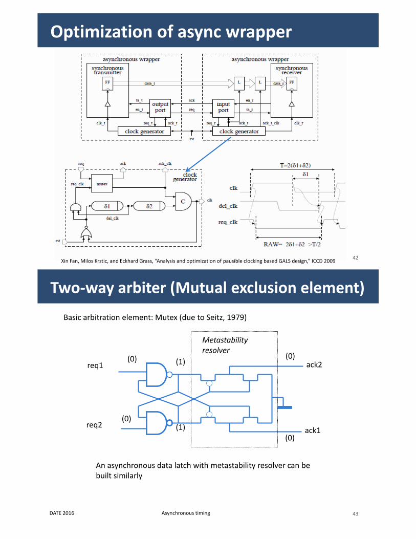
DATE 2016 Asynchronous timing 42
Optimization of async wrapper
Xin Fan, Milos Krstic, and Eckhard Grass, “Analysis and optimization of pausible clocking based GALS design,” ICCD 2009
Two-way arbiter (Mutual exclusion element)
req1
req2
ack2
ack1
(0)
(0)
(1)
(1)
(0)
(0)
Basic arbitration element: Mutex (due to Seitz, 1979)
An asynchronous data latch with metastability resolver can be built similarly
Metastability resolver
43 DATE 2016 Asynchronous timing

Design Automation
DATE 2016 Asynchronous timing 44
Design automation paradigms
• Synthesis of asynchronous controllers
• Logic synthesis from Petri nets or asynchronous FSMs
• Syntax-directed translation
• Correct-by-construction composition of handshake components
• De-synchronization
• Automatic transformation from synchronous to asynchronous
DATE 2016 Asynchronous timing 45

Synthesis of asynchronous controllers
DATE 2016 Asynchronous timing 46
DSr
LDS
LDTACK
D
DTACK
LDS+ LDTACK+ D+ DTACK+ DSr- D-
DTACK-
LDS- LDTACK-
DSr+
Device
LDS
LDTACK
D
DSr
DSw
DTACK
VME Bus Controller
Data
Transceiver
Bus
Synthesis of asynchronous controllers
DATE 2016 Asynchronous timing 47
LDS+ LDTACK+ D+ DTACK+ DSr- D-
DTACK-
LDS- LDTACK-
DSr+
DTACK D
DSr
LDS
LDTACK
Example: Petrify

Workcraft tool
• Workcraft is a software package for graphical edit, analysis, synthesis and visualisation of asynchronous circuit behaviour
• Petrify, MPSAT, plus a few other tools are part of it as plug-ins
• It is based in Java tools
• Can be downloaded from http://workcraft.org/
• And installed in 10 minutes
• There is a simple to use tutorial for that
48 DATE 2016 Asynchronous timing
Workcraft
DATE 2016 Asynchronous timing 49

Conclusions
• Asynchrony offers flexibility in time • Modularity • Dynamic adaptability • Tolerance to variability
• Better optimization of power/performance • Facilitates near and sub-threshold modes • Facilitates easier power-gating
• Why isn’t it an important trend in circuit design? • Lack of commercial EDA support (timing sign-off) • Designers do not feel comfortable with “unpredictable”
timing • Other aspects: testing, verification, …
• De-synchronization might be a viable solution
DATE 2016 Asynchronous timing 50
Some references
• General Async Design: J. Sparsø and S.B. Furber, editors. Principles of
Asynchronous Circuit Design, Kluwer Academic Publishers, 2001.
(electronic version of a tutorial based on this book can be found on:
http://www2.imm.dtu.dk/pubdb/views/edoc_download.php/855/pdf/imm855.
• Async Control Synthesis: J. Cortadella, M. Kishinevsky, A. Kondratyev,
L. Lavagno, and A. Yakovlev. Logic Synthesis of Asynchronous Controllers
and Interfaces. Springer-Verlag, 2002. (Petrify software can be downloaded
from: http://www.lsi.upc.edu/~jordicf/petrify/)
• Arbiters and Synchronizers: D.J. Kinniment, Synchronization and
Arbitration in Digital Systems, Wiley and Sons, 2007 (a tutorial on arbitration
and synchronization from ASYNC/NOCS 2008 can be found:
http://async.org.uk/async2008/async-nocs-slides/Tutorial-
Monday/Kinniment-ASYNC-2008-Tutorial.pdf)
• Asynchronous on-chip interconnect: John Bainbridge, Asynchronous
System-on-Chip Interconnect, BCS Distinguished Dissertations, Springer-
Verlag, 2002 (electronic version of the PhD thesis can be found on:
http://intranet.cs.man.ac.uk/apt/publications/thesis/bainbridge00_phd.php)
DATE 2016 Asynchronous timing 51

Metastability and
Clock Domain Crossing
David M. Zar
Blendics, Inc.

Modern Clocking Strategies:Metastability and
Clock Domain Crossing
David M. Zar
Blendics, Inc
• Clock Domain Crossing (CDC) Fundamentals
• How Synchronizers Can Fail
• Common Synchronizer Structures
• Analysis of Synchronizer Failure
• Good Synchronizers
Overview
DATE 2016 Metastability and Clock Domain Crossing 1

• A CDC occurs whenever a signal crosses from one clock domain to another
• Any data input not synchronous to a clock is a CDC, in general (e.g. an asynchronous input)
• In modern SOCs, there could be hundreds, or even thousands, of CDCs ocurring between any number of disparate clock domains
• If any of these CDCs are not dealt with, the circuit may fail due to a synchronization failure:
• Metastability failure or
• Under/over sampling failure
Clock Domain Crossing (CDC) Fundamentals
DATE 2016 Metastability and Clock Domain Crossing 2
• A violation of input timing at the synchronizer can cause the output of the synchronizer to go metastable:
• During the transition, the output must not be sampled at the destination until it has resolved
Metastability Failure
DATE 2016 Metastability and Clock Domain Crossing 3
Clock
Data
Edges too close
OutputInvalid logic level
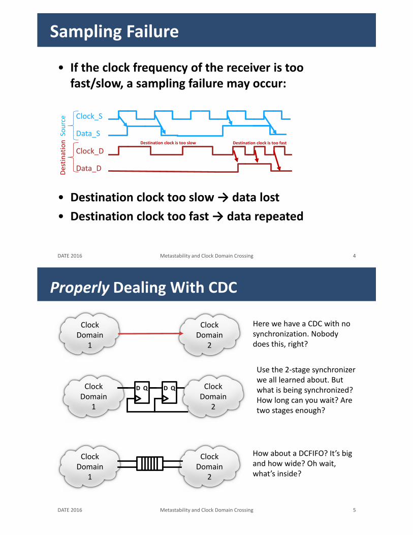
• If the clock frequency of the receiver is too fast/slow, a sampling failure may occur:
• Destination clock too slow → data lost
• Destination clock too fast → data repeated
Sampling Failure
DATE 2016 Metastability and Clock Domain Crossing 4
Clock_S
Data_S
Clock_D
Data_D
Sou
rce
Des
tin
atio
n Destination clock is too slow Destination clock is too fast
Properly Dealing With CDC
DATE 2016 Metastability and Clock Domain Crossing 5
ClockDomain
1
ClockDomain
2
Here we have a CDC with no synchronization. Nobody does this, right?
ClockDomain
1
ClockDomain
2
How about a DCFIFO? It’s big and how wide? Oh wait, what’s inside?
ClockDomain
1
ClockDomain
2
D Q D Q
Use the 2-stage synchronizer we all learned about. But what is being synchronized? How long can you wait? Are two stages enough?

Properly Dealing With CDC
DATE 2016 Metastability and Clock Domain Crossing 6
ClockDomain
1
ClockDomain
2
Here we have a CDC with no synchronization. Nobody does this, right?
ClockDomain
1
ClockDomain
2
How about a DCFIFO? It’s big and how wide? Oh wait, what’s inside?
ClockDomain
1
ClockDomain
2
D Q D Q
Use the 2-stage synchronizer we all learned about. But what is being synchronized? How long can you wait? Are two stages enough?
• So it seems until you look under the covers:
• This still can have a synchronizer failure!
Handshaking Solves the CDC Problem! [?]
DATE 2016 Metastability and Clock Domain Crossing 7
Clock Domain
1
Clock Domain
2
D QD Q
Q D Q D
Request
ACK
Data

• The good news is that identifying CDCs is easy:• Designer should know, right:
• Static analysis – did you find them all?• Power islands – dynamic powering up/down?• Reset – where does it go and when?
• Helpful tools:• Blue Pearl ACE• Mentor Graphics Questa CDC• Real Intent Meridian• Synopsys SpyGlass CDC (Formerly Atrenta)• vSync Circuits vChecker• Others…
CDC Identification
DATE 2016 Metastability and Clock Domain Crossing 8
• If you have removed all unnecessary CDCs and then properly added synchronization at the remaining CDCs, your synchronizer may still fail
• What is a synchronizer failure?
• A synchronizer failure is when the output fails to resolve to a valid logic level by a certain point in time (typically clock period minus setup time)
• Is caused by the inputs changing at the wrong time (like violating setup or hold time at a flip-flop)
Analysis of Synchronizer Failure
DATE 2016 Metastability and Clock Domain Crossing 9
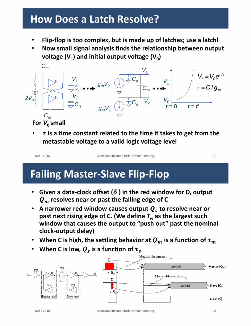
How Does a Latch Resolve?
DATE 2016 Metastability and Clock Domain Crossing 10
For V0 small
• Flip-flop is too complex, but is made up of latches; use a latch!• Now small signal analysis finds the relationship between output
voltage (V1) and initial output voltage (V0)
gmV1
Cn
Cn
Cm
Cm
V1
V2
Cn
Cn
V1
gmV2Cm
V2t = 0
V02V0
t = t’
V1
/t
01 eVV
mgC /
• 𝝉 is a time constant related to the time it takes to get from the metastable voltage to a valid logic voltage level
Failing Master-Slave Flip-Flop
DATE 2016 Metastability and Clock Domain Crossing 11
• Given a data-clock offset (𝜹 ) in the red window for D, output 𝑸𝒎 resolves near or past the falling edge of C
• A narrower red window causes output 𝑸𝒔 to resolve near or past next rising edge of C. (We define Tw as the largest such window that causes the output to “push out” past the nominal clock-output delay)
• When C is high, the settling behavior at 𝑸𝒎 is a function of 𝝉𝒎• When C is low, 𝑸𝒔 is a function of 𝝉𝒔
Qm Qs δ𝑚
δ𝑠
τ𝑠
τ𝑚
Master (Qm)
Slave (Qs)
Clock (C)

• So given that you can identify CDCs in circuits, and
• Given that you cannot guarantee they will always work,
• What are you to do?
• Give up?
• Pretend the problem won’t happen because you used a two flip-flop synchronizer?
• Design good synchronizers, use them, and analyze their failure rates to be sure you are at acceptable levels?
CDC Failure Analysis
DATE 2016 Metastability and Clock Domain Crossing 12
• For a given synchronizer• We can determine some
intrinsic parameters that govern how fast it resolves (τ and Tw)
• We can determine some extrinsic parameters that describe the environment (clock frequency, data arrival rates, etc.)
• We can then determine the failure rate for any particular synchronizer
Failure Analysis
DATE 2016 Metastability and Clock Domain Crossing 13

• We commonly use Mean Time Between Failures (MTBF) when speaking of synchronizer failures:
𝑴𝑻𝑩𝑭 =𝒆 ൗ𝑺 𝝉
𝑻𝒘𝒇𝒅𝒇𝒄S is the settling time by which the signal must be resolved,
fd is the data rate and fc is the sampling clock rate
• Failure Rate = 1/MTBF (also known as Failures In Time, or FIT)• For N such synchronizers in C chips shipped, the total Failure Rate is
NC/MTBF (or many orders of magnitude higher than for a single synchronizer!)
• Pr(safe) – Probability of Being Safe – measures the probability that all units in the field perform safely through the average lifetime of said units:
𝑷𝒓 𝒔𝒂𝒇𝒆 = 𝐞𝐱𝐩−𝑵𝑪𝑳
𝑴𝑻𝑩𝑭Where 𝑳 𝐢𝐬 𝐭𝐡𝐞 𝐚𝐯𝐞𝐫𝐚𝐠𝐞 𝐥𝐢𝐟𝐞𝐭𝐢𝐦𝐞 𝐨𝐟 𝐚 𝐮𝐧𝐢𝐭
Failure Rate/MTBF/Pr(safe)
DATE 2016 Metastability and Clock Domain Crossing 14
• MTBF is not how long it will take, on average, for your circuit to fail.• MTBF of 100 years is fine for one failure in 100 years and is
acceptable for my calculator.
• MTBF is not the expected lifetime of your device.• MTBF of 5 years for a cell phone is fine if nobody uses it for
that long.
• MTBF is not the service time of your device.• MTBF of 2 years for the IV pump is acceptable if we will service
it every year, test it, etc.
• For example, an MTBF of 10 years implies that:• In the first year, we expect ~10% of our devices to fail,
• After 10 years, we expect ~63% of our devices to fail!
MTBF/Failure Rate Fallacies
DATE 2016 Metastability and Clock Domain Crossing 15

• It is imperative to know the MTBF for your synchronizer:
• Turns out, as feature size goes below about 65 nm, 𝝉starts to increase (lowering MTBF) relative to FO4 delay
Know Your MTBF
DATE 2016 Metastability and Clock Domain Crossing 16
From Beer, et al. Devolution of Synchronizers
• Process variability affects MTBF
• For example, 𝝉 𝐢𝐬 𝐬𝐞𝐧𝐬𝐢𝐭𝐢𝐯𝐞 𝐭𝐨 Vt
Know Your MTBF (2)
DATE 2016 Metastability and Clock Domain Crossing 17

• Vdd matters, too
Know Your MTBF (3)
DATE 2016 Metastability and Clock Domain Crossing 18
• The duty cycle of the clock can affect MTBF in master-slave type flip-flops/synchronizers
• Typically, 𝝉 is assumed to be only a function of the master (or slave) of a master-slave FF; This is not the case.
𝜏𝑒𝑓𝑓 =𝛼
𝜏𝒎+
1 − 𝛼
𝜏𝒔
−1
• Where 𝝉𝒆𝒇𝒇 is the effective 𝝉 𝐨𝐟 𝐭𝐡𝐞 device.
• 𝜶 𝐢𝐬 𝐭𝐡𝐞 𝐝𝐮𝐭𝐲 𝐜𝐲𝐜𝐥𝐞 (e.g. 0.4 means the clock is high for 40% of the clock period)
• 𝝉𝒎 is the 𝝉 for the master latch; 𝝉𝒔 is the 𝝉 for the slave latch
Know Your MTBF (4)
DATE 2016 Metastability and Clock Domain Crossing 19

Effective 𝝉 Example
DATE 2016 Metastability and Clock Domain Crossing 20
• A 𝝉𝒆𝒇𝒇 will vary between the 𝝉 values of the master and the slave, being
their harmonic mean at a 50% duty cycle when the two 𝝉 values are close to each other.
• Things are more interesting when the 𝝉 values are very different
0 0.2 0.4 0.6 0.8 120
40
60
80
100
120
140
160
Duty cycle-
e
ffe
ctive (
pse
c)
Very Different𝝉𝒎 = 𝟏𝟓𝟎 𝐩𝐬, 𝝉𝒔 = 𝟑𝟎 𝐩𝐬
0 0.2 0.4 0.6 0.8 160
62
64
66
68
70
72
74
76
78
80
Duty cycle -
effe
ctiv
e
Nearly the Same𝝉𝒎 = 𝟖𝟎 𝐩𝐬, 𝝉𝒔 = 𝟔𝟎 𝐩𝐬
• Finally, most published MTBF models are not correct for multi-stage FF-based synchronizers (see Beer, MTBF Bounds for Multistage Synchronizers)
Know Your MTBF (5)
DATE 2016 Metastability and Clock Domain Crossing 21
0.6 0.8 1 1.2 1.4 1.6 1.8 2
100
1010
1020
1030
T (nsec)
MT
BF
(yea
rs)
Calculation (17)
[14] Master
[14] Slave
[14] Effective
[8] Master
[8] Slave
[8] Effective
[7] Master
[7] Slave
[7] Effective
Simulations
1 1 1 1 1 1.0001
105
106
107
108
109
1010
T (nsec)
MT
BF
(yea
rs)
Calculation (17)
[14] Master
[14] Slave
[14] Effective
[8] Master
[8] Slave
[8] Effective
[7] Master
[7] Slave
[7] Effective
Simulations
1 1 1 1 1 1.0001
105
106
107
108
109
1010
T (nsec)
MT
BF
(yea
rs)
Calculation (17)
[14] Master
[14] Slave
[14] Effective
[8] Master
[8] Slave
[8] Effective
[7] Master
[7] Slave
[7] Effective
Simulations

(Or… Why You Should Never Use a Data Flip-Flop as a Synchronizer)• Data Flip-Flop
• Used for temporary storage of data• Prevent data values from corruption during a clock cycle• Hold data values for multiple clock cycles
• Designed for deterministic cycle-to-cycle operation• Implies large setup/hold times
• Synchronizer Flip-Flop• Used to minimize Pr(failure)
• Data/clock may arrive at any time which may cause a setup/hold violation at a following data flip-flop
• Needs to preserve data transition sequence• No guarantee of deterministic cycle-to-cycle timing
Good Synchronizers
DATE 2016 Metastability and Clock Domain Crossing 22
Data Flip-Flops Vs. Synchronizer Flip-Flops
DATE 2016 Metastability and Clock Domain Crossing 23
In
Clk
Different performance characteristics to optimize based on FF use:
tpd tsu th τ Tw
Data FF minimize minimize 0 - -
Synchronizer FF - - 0 minimize minimize
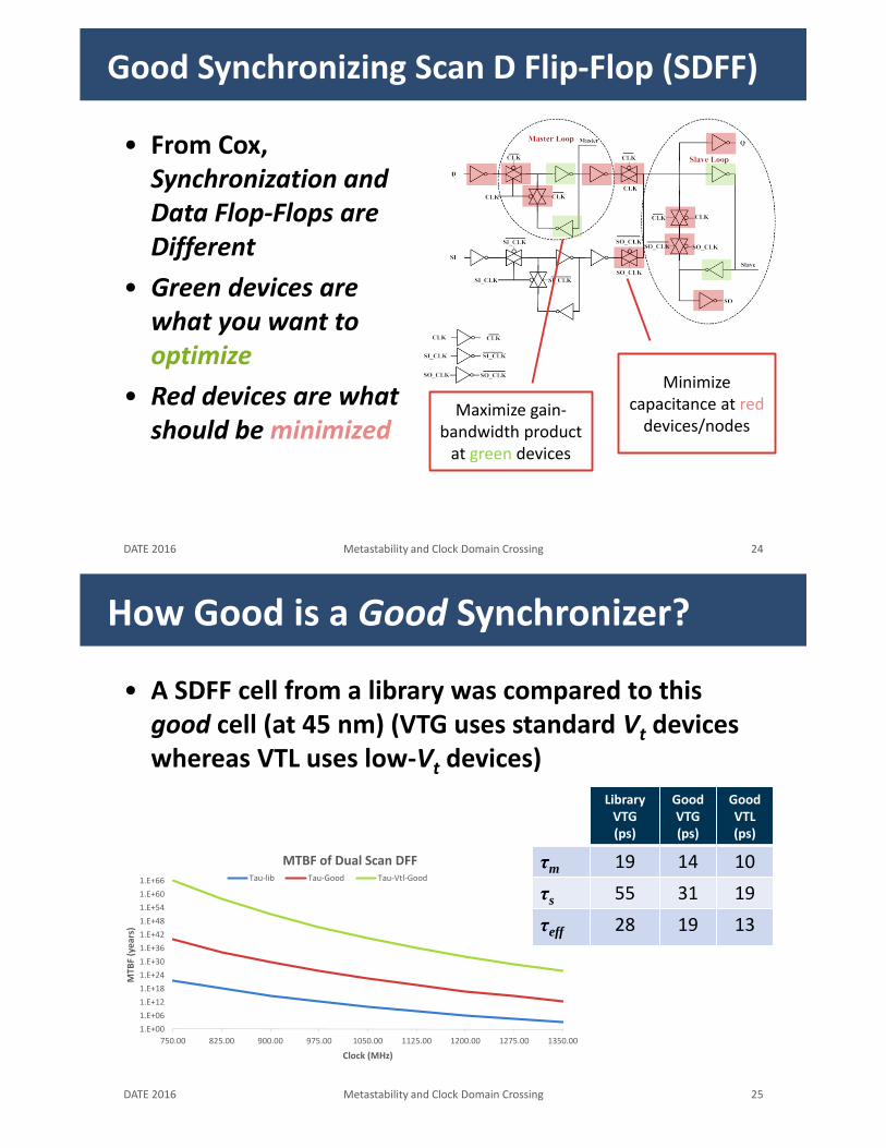
• From Cox, Synchronization and Data Flop-Flops are Different
• Green devices are what you want to optimize
• Red devices are what should be minimized
Good Synchronizing Scan D Flip-Flop (SDFF)
DATE 2016 Metastability and Clock Domain Crossing 24
Minimize capacitance at red
devices/nodesMaximize gain-
bandwidth product at green devices
• A SDFF cell from a library was compared to this good cell (at 45 nm) (VTG uses standard Vt devices whereas VTL uses low-Vt devices)
How Good is a Good Synchronizer?
DATE 2016 Metastability and Clock Domain Crossing 25
Library VTG(ps)
GoodVTG(ps)
GoodVTL(ps)
τm 19 14 10
τs 55 31 19
τeff 28 19 13
1.E+00
1.E+06
1.E+12
1.E+18
1.E+24
1.E+30
1.E+36
1.E+42
1.E+48
1.E+54
1.E+60
1.E+66
750.00 825.00 900.00 975.00 1050.00 1125.00 1200.00 1275.00 1350.00
MTB
F (y
ear
s)
Clock (MHz)
MTBF of Dual Scan DFFTau-lib Tau-Good Tau-Vtl-Good

• You want a large MTBF
• So you need small 𝝉
• Use low-Vt transistors if you can
• Use largest Vdd you can
• Reduce capacitance on nodes in regenerative loops -including output node(s)
• Design a custom synchronization flip-flop (as in reference: Synchronization and Data Flop-Flops are Different)
• BEWARE: Many clever synchronizing flop-flop designs have new issues. Why be complicated when you can analyze?!
Design for Good Synchronization
DATE 2016 Metastability and Clock Domain Crossing 26
• To properly handle the CDC in your circuit, you need to identify all such occurrences
• Then you need to ensure a proper synchronization mechanism is used
• Then you need to determine the MTBF/FIT for each CDC
• Finally, you can calculate the MTBF/FIT/Pr(safe) for the entire circuit based on the individual MTBF/FIT, the number of each, the length of service and the number of copies you expect to be in use
So…
DATE 2016 Metastability and Clock Domain Crossing 27
Questions
DATE 2016 Metastability and Clock Domain Crossing 28
• Beer, S. et al., MTBF Bounds for Multistage Synchronizers, ASYNC2013, http://ieeexplore.ieee.org/xpl/login.jsp?tp=&arnumber=6546190&url=http%3A%2F%2Fieeexplore.ieee.org%2Fxpls%2Fabs_all.jsp%3Farnumber%3D6546190
• Beer, S et al., The Devolution of Synchronizers, http://kolodny.eew.technion.ac.il/files/2013/08/The-devolution-of-synchronizers-ASYNC-2010.pdf
• Beer, S et al., Supply Voltage and Temperature Influence in Circuit Synchronization, DATE2013, http://webee.technion.ac.il/~ran/papers/BeerVoltageTempVariations.pdf
• Cox, J, Beware of Parameter Variability in Clock Domain Crossings, SemiWiki.com, 2015 https://www.semiwiki.com/forum/content/4625-beware-parameter-variability-clock-domain-crossings.html?s=30b01668a0a490331fd3f496f7a4f86a
• Cox, J, et al., Synchronization and Data Flop-Flops are Different, ASYNC 2015, http://ieeexplore.ieee.org/xpl/login.jsp?tp=&arnumber=7152686&url=httpA%2F%2Fieeexplore.ieee.org%2Fxpls%2Fabs_all.jsp%3Farnumber%3D7152686
• Cox, J, Synchronizer Reliability Metrics, 2014, SemiWiki, https://www.semiwiki.com/forum/content/3294-synchronizer-reliability-metrics.html
• Golson, S, Synchronization and Metastability, 2014, http://blendics.com/wp-content/uploads/2015/06/golson_snug14.pdf
References
DATE 2016 Metastability and Clock Domain Crossing 29

Adaptive Clocking
Jordi Cortadella
Universitat Politecnica de Catalunya

Modern Clocking Strategies:
Adaptive Clocking
Jordi CortadellaUniversitat Politècnica de Catalunya
Outline
• Sources of variability– Static/dynamic, local/global
• Reducing Margins for Static and Slow Variability– Binning– Voltage-Frequency Scaling
• Reducing Margins for Fast Variability– Resilient circuits– Adaptive Clocks
• Reactive Clocks and GALS
DATE 2016 Adaptive Clocking 2

The cost of variability
DATE 2016 Adaptive Clocking 3
margins
frequency
Goal:Reduce margins
Impact:SpeedEnergy
Process variability
DATE 2016 Adaptive Clocking 4
Fast
Typical
Slow
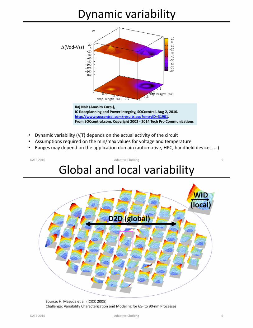
Dynamic variability
DATE 2016 Adaptive Clocking 5
Raj Nair (Anasim Corp.),IC floorplanning and Power Integrity, SOCcentral, Aug 2, 2010.http://www.soccentral.com/results.asp?entryID=31901. From SOCcentral.com, Copyright 2002 - 2014 Tech Pro Communications
(Vdd-Vss)
• Dynamic variability (V,T) depends on the actual activity of the circuit• Assumptions required on the min/max values for voltage and temperature• Ranges may depend on the application domain (automotive, HPC, handheld devices, …)
Global and local variability
DATE 2016 Adaptive Clocking 6
Source: H. Masuda et al. (ICICC 2005)Challenge: Variability Characterization and Modeling for 65- to 90-nm Processes
D2D (global)
WID(local)

12112
Timing: setup constraint
DATE 2016 Adaptive Clocking
Comb. Logic
Two competing paths:• Launching path• Capturing path
Launching path < Capturing path + Period2PLL
7
PVTA variability
No variability(or very little) +
Margins
Margins for Variability
DATE 2016 Adaptive Clocking 8
Q
D
D Q
Period
clock-data compensation
launching path
margin
capturing path
Q
D
D Q
Period
time
Margins are required to account for theworst-case variability (static and dynamic)

Variability and margins
DATE 2016 Adaptive Clocking 9
StaticDynamic
Slow (ms) Fast (ns)
Global (corners) PV VTA V
Local (OCV) PV VTA V
Voltage variability:• Static IR drop• Dynamic IR drop• Inductive noise (Ldi/dt)
(P:Process; V: Voltage; T: Temperature; A: Aging)
Reducing Margins forStatic and Slow Variability

V-F operation points
DATE 2016 Adaptive Clocking 11
Voltage
Frequency
Nominalvoltage
Speed binning
DATE 2016 Adaptive Clocking 12
Voltage
Frequency
𝐹1 𝐹2 𝐹3
Nominalvoltage

Voltage binning
DATE 2016 Adaptive Clocking 13
Voltage
Frequency
𝑉1
𝑉2
𝑉3
Dynamic Voltage Frequency Scaling (DVFS)
DATE 2016 Adaptive Clocking 14
Voltage
Frequency
(𝑽𝟏, 𝑭𝟏)(𝑽𝟐, 𝑭𝟐)
(𝑽𝟑, 𝑭𝟑)
(𝑽𝟒, 𝑭𝟒)
(𝑽𝟓, 𝑭𝟓)
(𝑽𝟔, 𝑭𝟔)
DVFS Table
𝑉1 𝐹1
𝑉2 𝐹2
𝑉3 𝐹3
𝑉4 𝐹4
𝑉5 𝐹5
𝑉6 𝐹5
Open loop control (SW).(V,F) selected according to:
• Workload• Temperature• Power budget

DVFS scheme
DATE 2016 Adaptive Clocking 15
DVFSblock
L-SHIFTERS & CDC
V1VRM
V2VRM
(variable)
(fixed)
SW
AVS scheme
DATE 2016 Adaptive Clocking 16
AVSblock
V1VRM
V2VRM
(variable)
(fixed)
PMU
L-SHIFTERS & CDC
PerformanceMonitor
ClosedLoop
Control
• Every die works at its best (V,F) point (plus some guardband margins)• AVS can compensate slow variability (temperature, aging)

Performance monitors
• Estimate the voltage/frequency relationship of the actual silicon
• Examples:
DATE 2016 Adaptive Clocking 17
Counter Ref. Clock
Measure frequencyRing oscillator
1 1 1 1 1 1 1 1 0 0 0 0 0 0 0 0CLK
delay
Edge detector
Time-to-digital converter
Reducing Margins forFast Variability

Resilient circuits
DATE 2016 Adaptive Clocking 19
CLK
Data
CLK
CLK_del
Data
PP +
Error recovery
Different values
Conventional timing
Resilient timing
= Error
Mainflip-flop
Shadowlatchdelay
Main data
Shadow data
CLK
Data
Resilient circuits
DATE 2016 Adaptive Clocking 20
Source: D. Ernst et al.,Razor: circuit-level corrrection of timing errors for low-power operation,IEEE Micro, Nov-Dec 2004.

Resilient circuits: technical issues
DATE 2016 Adaptive Clocking 21
CLK
CLK_del
Data
PP +
Potentialmetastability
min shortpath
Error recovery(may take several cycles)
• Only critical flip-flops require shadow latches• Short paths must have a min delay• Metastability may take several cycles to resolve• Sophisticated error-recovery procedures are required
DATE 2016 Adaptive Clocking 22
Source: S. Das et al.,RazorII: In Situ Error Detection and Correction for PVT and SER Tolerance.IEEE JSSC 44(1), Jan 2009.

Resilient circuits
DATE 2016 Adaptive Clocking 23
Resilientcircuit
VddVRM
ErrorMonitor
ClosedLoop
Control
𝑃𝑒𝑓𝑓 = 𝑃 1 + 𝑛ℰ
probabilityof error
num cycles forerror recovery
Closed Loop Control:• Raise voltage if too many errors• Lower voltage if too few errors
Error recovery mechanism:• Reuse existing checkpoint schemes in advanced processors
Schemes with resilient circuits
• ARM + University of Michigan– Different variations: Razor I, Razor II, Bubble Razor
• Intel:– Transition Detector with Time Borrowing (TDTB)
– Double Sampling with time Borrowing (DSTB)
• Using pausable clocks and metastability detectors– SafeRazor (Torino, Technion and UPC)
– Blade (USC)
DATE 2016 Adaptive Clocking 24

Voltage droops
DATE 2016 Adaptive Clocking 25
Source: Y. Kim et al.,Automating Stressmark Generation for Testing Processor Voltage Fluctuations,IEEE Micro, July-August 2013.
Voltage droops are the main source of fast variability
Power Delivery Network
DATE 2016 Adaptive Clocking 26
Source: Jitesh ShahFloorplanning A Power Delivery Network With Spice Electronic DesignJuly 24, 2008http://electronicdesign.com/energy/floorplanning-power-delivery-network-spice

PDN model
DATE 2016 Adaptive Clocking 27
Local Global
Adaptive Clock
DATE 2016 Adaptive Clocking 28
Vdd Droop detected
Period stretched New frequency
Mechanisms are needed for:• Droop detection• Clock period stretching• Frequency reduction
DLL
CLK

AMD Steamroller
DATE 2016 Adaptive Clocking 29
Source: K. Wilcox et al.Steamroller Module and Adaptive ClockingSystem in 28nm CMOSIEEE JSSC 50(1), Jan 2015.
Intel Adaptive Clock
DATE 2016 Adaptive Clocking 30
Source: K.A. Bowman et al.A 22 nm All-Digital Dynamically Adaptive ClockDistribution for Supply Voltage Droop Tolerance,IEEE JSSC 48(4), April 2013.

Intel Adaptive Clock
DATE 2016 Adaptive Clocking 31
Margins for Adaptive Clocks
DATE 2016 Adaptive Clocking 32
Clk
Nominal voltage
droop detection threshold
Reaction time margins savedby adaptive clock
Circuit Sensors
FrequencySynthesizer
Control
Other approaches:
• N. Kurd, P. Mosalikanti, M. Neidengard, J. Douglas, and R. Kumar,Next generation Intel core micro-architecture (Nehalem) clocking,IEEE JSSC 44(4), 2009.
• K. Chae and S. Mukhopadhyay, All-digital adaptive clocking totolerate transient supply noise in a low-voltage operation,IEEE TCAS II 59(12), 2012.
• C. Lefurgy, A. Drake, M. Floyd, M. Allen-Ware, B. Brock, J. Tierno,J. Carter, and R. Berry, Active guardband management in Power7+to save energy and maintain reliability, IEEE Micro 33(4), 2013.

Reactive Clocks
Mechanisms to reduce margins
DATE 2016 Adaptive Clocking 34
StaticDynamic
Slow (ms) Fast (ns)
Global (corners) PV VTA V
Local (OCV) PV VTA V
Mechanism Reduces margins for …
Binning, DVFS (open loop) Static variability
AVS (close loop) + Slow global variability
Adaptive Clocks + Fast global variability (moderate)
Reactive Clocks + Fast global variability (aggressive)
Resilient circuits Any variability (aggressive)

12112
Timing: setup constraint
DATE 2016 Adaptive Clocking
Comb. Logic
Two competing paths:• Launching path• Capturing path
Launching path < Capturing path + Period2PLL
35
PVTA variability
No variability(or very little) +
Margins
Reactive Clock
DATE 2016 Adaptive Clocking
Comb. Logic
Launching path < Capturing path + Period
36
PVTA variability
+Margins

Variability: PLL vs. Reactive Clock
DATE 2016 Adaptive Clocking 37
Q
D
D Q
PLL period
Q
D
D Q
Reactive Clock
clock-data compensation
launching path
margin
capturing path
Q
D
D Q
PLL period
time
ReactiveClk (1.2V)
ReactiveClk (0.85V)
PLL vs. Reactive Clock
DATE 2016 Adaptive Clocking 38
30%PLL
(1.2V)

ReactiveClock
Reactive Clock
DATE 2016 Adaptive Clocking 39
PLL
Enable
Gain: 40% less Energy or1.6x speed-up
Pain: Negligible
Risk: Zero
• Original circuit not modified• Negligible area• Post-tapeout calibration (by SW)• Conventional timing (PrimeTime)
Clock domain
J. Cortadella, L. Lavagno, P. López, M. Lupon,A. Moreno, A. Roca, and S. S. Sapatnekar.Reactive clocks with variability-tracking jitter.ICCD 2015.
PLL Rclk
PLL vs. Reactive Clocks
DATE 2016 Adaptive Clocking 40
DUT
PLL Rclk
temperature
25oC 125oC75oCSPICE models
(65nm)
Slow125oC
Typical125oC
Timingsign-off
Slow75oC
Typical75oC
1.6x
1.2x

sign-off
PLL Rclk
PLL vs. Reactive Clocks
DATE 2016 Adaptive Clocking 41
DUT
PLL Rclk
temperature
25oC 125oC75oCSPICE models
(65nm)
-20%(1.07V)
-42%(0.91V)
Energy reduction(@iso-performance)
Synthesis of the Ring oscillator
DATE 2016 Adaptive Clocking 42
Library Corners
PLL period
De
lay
OCV
Programmable by SW

PLL
Enable
Clock domainCDC
CDC
CDC
Ring oscillator
Reactive Clock Domain
DATE 2016 Adaptive Clocking 43
CDC structures required for communication outside the clock domain
GALS with Reactive Clocks
DATE 2016 Adaptive Clocking 44
RO
RO
RO
RO
• A different Reactive Clock for each domain• Clock Domain Crossing structures between domains

Summary
DATE 2016 Adaptive Clocking 45
Ideal typical die(no PVT variability)
Slow die (sign-off)
Binning (or AVS)
Adaptive clock (tolerance to droops)
Resilient (Razor)
Reactive clock(ring oscillator)
Conclusions
• Moore’s law is (economically) over. It is time to exploit what is left in established nodes.
• What is left? Margins for variability.
• Dilemma: how to spend your money?
– introducing techniques to reduce margins, or
– moving to a new (expensive) technology node
DATE 2016 Adaptive Clocking 46