ieee transactions on nanotechnology, vol. …jmjornet/papers/2017/j7.pdf · ieee transactions on...
TRANSCRIPT

IEEE TRANSACTIONS ON NANOTECHNOLOGY, VOL. 16, NO. 6, NOVEMBER 2017 919
Nanodevice Arrays for Peripheral Nerve FascicleActivation Using Ultrasound Energy-Harvesting
Michael Donohoe , Member, IEEE, Brendan Jennings, Member, IEEE, Josep Miquel Jornet , Member, IEEE,and Sasitharan Balasubramaniam, Senior Member, IEEE
Abstract—We propose the use of wireless, energy harvesting,implanted nanodevice arrays with electrodes for selective stimu-lation of peripheral nerves in the human body. We calculate theinput ultrasound energy and harvested power for single fixed-sizenanowire-based nanodevices at different tissue depths and com-pare these with the current and voltage levels required for periph-eral neural stimulation. We model the dimensioning of arrays ofnanodevices, embedded in biocompatible tissue patches, to meetthese neural stimulation requirements. Selectivity of activation ofparticular nerve bundles requires that the output voltage and cur-rent of the array can be varied to increase or decrease penetrationinto the neural tissue. This variation can be achieved by chang-ing the energized area of the array and/or by decreasing the in-cident ultrasound power. However, the array must be implantedhorizontally relative to the incident ultrasound as any tilting ofthe nanodevices will reduce the harvested energy. The proposedapproach provides a longer-term implant solution for nerve stim-ulation that allows the patient greater freedom of movement thanwith embedded tethered electrodes.
Index Terms—Energy harvesting, nanoscale devices, nerve stim-ulation, ultrasound.
I. INTRODUCTION
N EURAL tissue activation relies on the use of electricalcurrent to stimulate specific parts of the nervous system
in order to treat neurological conditions (e.g., Parkinson’s Dis-ease), nerve breakages resulting from accidents, or neural con-nectivity for prosthetics. Stimulation of motor nerves at presentis carried out by externally powered electrodes placed on theskin surface (transcutaneous) or under the skin (subcutaneous)
Manuscript received May 8, 2017; accepted June 26, 2017. Date of publicationJuly 5, 2017; date of current version November 8, 2017. This work was supportedin part by the Finnish Academy Research Fellow Programme under Project284531, in part by the Irish Higher Education Authority under the Programmefor Research in Third Level Institutions (PRTLI) cycle 5, which is funded by theEuropean Regional Development Fund, via the Telecommunications GraduateInitiative, and in part by the Science Foundation Ireland via the CONNECTResearch Centre under Grant 13/RC/2077. The review of this paper was arrangedby Associate Editor T. S. Wong. (Corresponding author: Michael Donohoe.)
M. Donohoe and B. Jennings are with the Telecommunications Software &Systems Group, Waterford Institute of Technology, Waterford, Ireland (e-mail:[email protected]; [email protected]).
S. Balasubramaniam is with the Telecommunications Software & SystemsGroup, Waterford Institute of Technology, Waterford, Ireland, and also with theDepartment of Electronic and Communication Engineering, Tampere Universityof Technology, Tampere 33720, Finland (e-mail: [email protected]).
J. M. Jornet is with the University at Buffalo, Buffalo, NY 14260 USA (e-mail:[email protected]).
Color versions of one or more of the figures in this paper are available onlineat http://ieeexplore.ieee.org.
Digital Object Identifier 10.1109/TNANO.2017.2723658
in closer proximity to muscles or nerves [1], [2]. Electrodes canbe single points or multiple arrays with variable voltage andcurrent control. The stimulus levels for these electrodes can beminimised by placing them as close as possible to the mainnerve tissue that needs to be stimulated. One type of electrode,the cuff electrode, can be wrapped around larger nerves [3] tominimise the applied voltage and current levels. The majorityof these solutions require implanted electrodes that are wiredto a power and control unit to deliver measured amounts ofvoltage and current [4] for functions such as deep brain stim-ulation, spinal cord stimulation, cochlear implants and cardiacpacemakers. A more advanced system for detecting brain activ-ity and then transmitting locomotion signals wirelessly to thelower spinal cord is described by Capogrosso et al. [5]. Bat-tery powered modules are used for signal detection and neuralstimulation while external systems provide signal processingand protocol transmission. Smaller scale components and effi-cient powering would greatly enhance the deployment of suchadvanced prosthetics.
A major limitation of such solutions is the practicality ofdevices that can be implanted within patients and enable themto live a normal lifestyle. The challenges include (i) the ability toembed the device for longer-term deployment, where the devicescan harvest energy from either the environment or an externalsource, avoiding the need for tethered wires, and (ii) ensuringthat the device can be easily inserted into the nervous system andused to stimulate specific nerve bundles (e.g., along the elbow,spinal cord), while minimizing any stress on the tissue.
In this article, we address these challenges by proposingand modelling the use of nanoscale devices (“nanodevices”)that can be safely implanted into patients for the longer-termstimulation of selected peripheral nerve fascicles. The overallscenario is illustrated in Fig. 1, where a nanodevice array isembedded into a polymer-based patch of bio-compatible tis-sue [6], and placed against a nerve’s outer layer (Epineurium).The nanodevice harvests its energy from ultrasound waves thatare emitted by a portable external source. The use of wire-less powering and biocompatible materials will provide greaterlongevity of components, though we do not have projectionsfor the ultimate longevity of such a device. The patch must beboth bio-compatible (to resist rejection, inflammation and bio-fouling) and non-degradable. Polymer-based bio-compatiblematerials specifically for substrates, structures and packagingare surveyed by Qin et al. [6]. They show how these materi-als can meet the requirements of implantable biosensors and
1536-125X © 2017 IEEE. Personal use is permitted, but republication/redistribution requires IEEE permission.See http://www.ieee.org/publications standards/publications/rights/index.html for more information.

920 IEEE TRANSACTIONS ON NANOTECHNOLOGY, VOL. 16, NO. 6, NOVEMBER 2017
Fig. 1. Bio-compatible patch containing nanodevice array powered by exter-nally generated ultrasonic waves. The array sends current pulses to stimulatespecific fascicles (nerve fibre bundles).
Fig. 2. Block diagram of end-to-end path from the ultrasound source throughskin/fat and a nanodevice array resulting in the generation of an electrical currentto stimulate the nerve fascicles.
describe different packaging methods. Polymer based packag-ing will also have acoustic impedance similar to human tissue(see Section III-A) and will have a minimal impact on the per-formance of the array. The end-to-end power transfer process,illustrated in Fig. 2, shows the external ultrasound source emit-ting waves that bend the piezoelectric nanowires in each of thenanodevices in the patch. The harvested ultrasound energy isconverted by the piezoelectric nanowires and releases an elec-tronic pulse that stimulates nerve fascicles through an electrode.However, the nanodevices must harvest sufficient power for re-leasing the required threshold amount of current to stimulatespecific nerve bundles. In previous work [7] we reported on aninitial investigation of the use of ultrasounds to power subcuta-neous nanowire-based nanodevices. That investigation showedhow lower ultrasound frequencies provided better tissue pene-tration and more energy per cycle to bend nanowires. Here weextend that work by (i) calculating the output voltage and currentof a nanodevice relative to the input ultrasound intensity and (ii)modelling the use of coupled nanodevices for selective neuralstimulation particularly in the fascicles of the peripheral nervesof the wrist and forearm that control arm and hand movements:the radial, median and ulnar. The main competitive advantageof our proposed approach, based on the use of a synthetic patcharray composed of nanodevices for stimulation, is the ability tostimulate nerve fascicles at different depths by varying the in-tensity of the incident ultrasound, or spatially targeting specificnanodevices on the patch. The piezoelectric nanowires can re-spond to lower ultrasound frequencies that can penetrate througha greater depth of tissue than higher frequencies.
The article is organised as follows: the architecture ofenergy-harvesting nanodevices using ultrasounds is outlined inSection II; the transmission of ultrasound energy through hu-man tissue and the power output of nanodevices is analysed inSection III; the deployment for neural stimulation is modelledin Section IV; and our conclusions are presented in Section V.
II. NANODEVICE ENERGY HARVESTING
Our proposed nanodevice must convert incident ultrasoundsinto mechanical vibrations and then into piezoelectric energy(Fig. 2). There are two main methods for harvesting ultra-sounds: resonant piezoelectric crystals or vibrating piezoelectricnanowires. The size of a resonant crystal depends on the fre-quency of the ultrasound: the higher the frequency, the thinnerthe crystal. The powering of sensors embedded in tissue usingresonant lead zirconate titanate (PZT) crystals has previouslybeen investigated by Ozeri and Schmilovitz [8], using a fre-quency of 673 kHz. These devices are at a macro scale (cm2)and not suitable for the miniature devices that we are targetingfor our patch. A cuff electrode powered by a PZT crystal, oper-ating at 1 MHz was also demonstrated by Larson and Towe [9].Simple half-wave rectification of the output AC voltage with asingle diode provided a stimulus pulse to the sciatic nerve of arat. The output power and successful operation depend criticallyon the positioning and alignment of the crystal, which could eas-ily be changed in a live body. The use of micro-scale resonantcrystals (“neural dust”) for neural recording using ultrasoundpowering and backscatter was proposed by Seo et al. [10]. Therecording principle has been demonstrated for peripheral nerves[11] though the available components are at millimetre scale atpresent. For smaller scale operation, an energy harvesting res-onant crystal would have dimensions in the micrometre scale,which would imply a resonant frequency in the 10 MHz orgreater range; such a high frequency of ultrasound would bestrongly absorbed by human tissue (see Section III-A) so minia-ture resonant crystal harvesters could only be deployed at veryshallow skin depths (e.g., 2 mm). Therefore, for deeper pene-tration using lower ultrasound frequencies, we consider piezo-electric zinc oxide (ZnO) nanowires that can vibrate in responseto a range of ultrasound frequencies [7] and produce variableamounts of current and voltage.
A. Piezoelectric ZnO Nanowires
We use an analytical perturbation model for bending a ZnOnanowire developed by Gao and Wang [12]. The nanowire ismodelled as a thin cylindrical rod with a specific modulus ofelasticity (Young’s modulus). Bending a nanowire requires theapplication of a force that is countered by the elasticity ofthe nanowire. If a constant force F is applied until a bend-ing before discharge ym (as depicted in Fig. 3) is achieved, thenthe balance of forces is as follows:
F =3Y Iym
L3 . (1)
In this case Y is the nanowire’s Young’s modulus, I is the areamoment of inertia and L is the nanowire length. The bendingis directly proportional to the applied force. The energy (work)ΔE required to bend the nanowire by an amount ym is:
ΔE =3Y Iy2
m
2L3 . (2)
The work is proportional to the square of the displacement.The voltage V is approximately linear over the range of appliedforces, as analysed by Hinchet et al. [13] and can be expressed
DONOHOE et al.: NANODEVICE ARRAYS FOR PERIPHERAL NERVE FASCICLE ACTIVATION USING ULTRASOUND ENERGY-HARVESTING 921
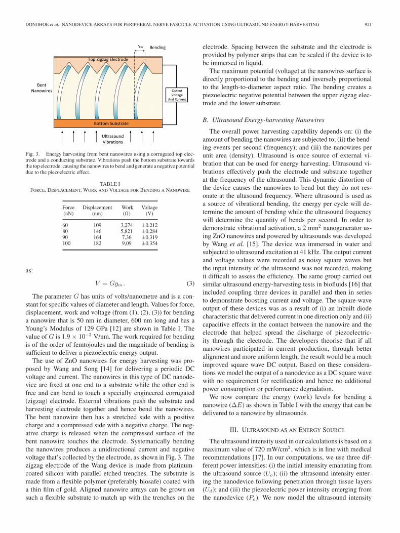
Fig. 3. Energy harvesting from bent nanowires using a corrugated top elec-trode and a conducting substrate. Vibrations push the bottom substrate towardsthe top electrode, causing the nanowires to bend and generate a negative potentialdue to the piezoelectric effect.
TABLE IFORCE, DISPLACEMENT, WORK AND VOLTAGE FOR BENDING A NANOWIRE
Force Displacement Work Voltage(nN) (nm) (fJ) (V)
60 109 3,274 ±0.21280 146 5,821 ±0.28490 164 7,36 ±0.319100 182 9,09 ±0.354
as:
V = Gym . (3)
The parameter G has units of volts/nanometre and is a con-stant for specific values of diameter and length. Values for force,displacement, work and voltage (from (1), (2), (3)) for bendinga nanowire that is 50 nm in diameter, 600 nm long and has aYoung’s Modulus of 129 GPa [12] are shown in Table I. Thevalue of G is 1.9 × 10⁻³ V/nm. The work required for bendingis of the order of femtojoules and the magnitude of bending issufficient to deliver a piezoelectric energy output.
The use of ZnO nanowires for energy harvesting was pro-posed by Wang and Song [14] for delivering a periodic DCvoltage and current. The nanowires in this type of DC nanode-vice are fixed at one end to a substrate while the other end isfree and can bend to touch a specially engineered corrugated(zigzag) electrode. External vibrations push the substrate andharvesting electrode together and hence bend the nanowires.The bent nanowire then has a stretched side with a positivecharge and a compressed side with a negative charge. The neg-ative charge is released when the compressed surface of thebent nanowire touches the electrode. Systematically bendingthe nanowires produces a unidirectional current and negativevoltage that’s collected by the electrode, as shown in Fig. 3. Thezigzag electrode of the Wang device is made from platinum-coated silicon with parallel etched trenches. The substrate ismade from a flexible polymer (preferably biosafe) coated witha thin film of gold. Aligned nanowire arrays can be grown onsuch a flexible substrate to match up with the trenches on the
electrode. Spacing between the substrate and the electrode isprovided by polymer strips that can be sealed if the device is tobe immersed in liquid.
The maximum potential (voltage) at the nanowires surface isdirectly proportional to the bending and inversely proportionalto the length-to-diameter aspect ratio. The bending creates apiezoelectric negative potential between the upper zigzag elec-trode and the lower substrate.
B. Ultrasound Energy-harvesting Nanowires
The overall power harvesting capability depends on: (i) theamount of bending the nanowires are subjected to; (ii) the bend-ing events per second (frequency); and (iii) the nanowires perunit area (density). Ultrasound is once source of external vi-bration that can be used for energy harvesting. Ultrasound vi-brations effectively push the electrode and substrate togetherat the frequency of the ultrasound. This dynamic distortion ofthe device causes the nanowires to bend but they do not res-onate at the ultasound frequency. Where ultrasound is used asa source of vibrational bending, the energy per cycle will de-termine the amount of bending while the ultrasound frequencywill determine the quantity of bends per second. In order todemonstrate vibrational activation, a 2 mm2 nanogenerator us-ing ZnO nanowires and powered by ultrasounds was developedby Wang et al. [15]. The device was immersed in water andsubjected to ultrasound excitation at 41 kHz. The output currentand voltage values were recorded as noisy square waves butthe input intensity of the ultrasound was not recorded, makingit difficult to assess the efficiency. The same group carried outsimilar ultrasound energy-harvesting tests in biofluids [16] thatincluded coupling three devices in parallel and then in seriesto demonstrate boosting current and voltage. The square-waveoutput of these devices was as a result of (i) an inbuilt diodecharacteristic that delivered current in one direction only and (ii)capacitive effects in the contact between the nanowire and theelectrode that helped spread the discharge of piezoelectric-ity through the electrode. The developers theorise that if allnanowires participated in current production, through betteralignment and more uniform length, the result would be a muchimproved square wave DC output. Based on these considera-tions we model the output of a nanodevice as a DC square wavewith no requirement for rectification and hence no additionalpower consumption or performance degradation.
We now compare the energy (work) levels for bending ananowire (ΔE) as shown in Table I with the energy that can bedelivered to a nanowire by ultrasounds.
III. ULTRASOUND AS AN ENERGY SOURCE
The ultrasound intensity used in our calculations is based on amaximum value of 720 mW/cm2 , which is in line with medicalrecommendations [17]. In our computations, we use three dif-ferent power intensities: (i) the initial intensity emanating fromthe ultrasound source (Uo ); (ii) the ultrasound intensity enter-ing the nanodevice following penetration through tissue layers(Ud ); and (iii) the piezoelectric power intensity emerging fromthe nanodevice (Po ). We now model the ultrasound intensity

922 IEEE TRANSACTIONS ON NANOTECHNOLOGY, VOL. 16, NO. 6, NOVEMBER 2017
Fig. 4. Plot of Ultrasound Intensity vs Skin/Fat and Muscle Depth. The rateof absorption is significantly higher for denser muscle tissue in comparison tothe less dense skin/fat.
entering the nanodevice; Section III-C models the power emerg-ing from the nanodevice.
A. Ultrasound Absorption and Reflection in Human Tissue
Externally applied ultrasound will penetrate initially throughseveral layers of human skin tissue. For peripheral nerve stimu-lation, the nanodevice would be embedded centimetres deep insubcutaneous fat. An ultrasonic beam of frequency f MHz withan initial intensity of Uo penetrating to a depth of d cm will havea resultant intensity of Ud :
Ud = Uo10−(αf d/10) . (4)
The absorption coefficient α, expresses the power loss andhas a value of 0.6 dB/cm/MHz for skin/fat and 1.8 dB/cm/MHzfor muscle [17]. Fig. 4 presents the ultrasound intensity withrespect to tissue depth (Ud ) and is based on (4), where theultrasound attenuation is calculated through 10 mm skin/fat andthen 10 mm muscle for four different ultrasound frequencies.The higher ultrasound frequencies are more strongly absorbedcompared to lower frequencies, particularly in the denser muscletissue.
Acoustic reflections at tissue interfaces (e.g., between fat andmuscle) are caused by differences in acoustic impedance (thedensity of the tissue multiplied by the speed of sound); the unitof acoustic impedance is the Rayl (kg.s−1 .m−2). The reflectionat an air/human tissue interface would result in up to 99% ofthe ultrasound being reflected because of the large differencein the acoustic impedance [17] (429 Rayl for air, 1.4 MRaylfor skin/fat). Consequently there should be no air gap betweenan ultrasound transducer and human tissue. For our nanodevicearray, the acoustic impedance of the synthetic patch and thenanodevice substrate should match the acoustic impedance ofbody tissue as closely as possible.
B. Ultrasound Cycle Energy
Initially, we model a single nanodevice that is perpendicularto the ultrasound vibrations (no tilt) and hence can intercept themaximum amount of ultrasound energy. The input intensity isfixed at 720 mW/cm2 , or 7.2 × 10 −9 W/μm2 , and the intensityat different depths is calculated using (4). At a fixed density of
Fig. 5. Plot of Ultrasound Intensity vs Angles of Tilt for a frequency of50 kHz and a skin/fat depth of 5 mm. The tilting of the nanodevice will have asignificant impact on the incident ultrasound intensity.
m nanowires per μm2 , the energy per nanowire per cycle, Enw ,at an ultrasound frequency of K cycles per second and intensityof Ud W/μm2 is calculated as follows:
Enw =Ud
mK. (5)
At 50 kHz the energy level is from 7.1 fJ to 6.7 fJ at 1cm and10 cm depth, respectively. The energy per cycle per nanowireat 1 MHz is initially over 20 times lower than at 50 kHz(0.03 fJ) and decreases more rapidly with depth. This means thatthe magnitude of 50 kHz ultrasound cycle energy per nanowireis comparable to the nanowire bending energies shown inTable I, but the 1 MHz cycle energies are too low to providesufficient bending. Consequently, we will assume the use of ul-trasound at a frequency of 50 kHz to power our nanodevices.By using a lower ultrasound frequency with lower tissue absorp-tion and short-duration (100 μs) infrequent pulses of ultrasound(See Section IV-A) we will minimise any possibility of tissueor nanodevice heating.
Maximum ultrasound power will be transferred to a nanode-vice if the incident beam is perpendicular to the device substrateand hence strike the full nanodevice area. If a nanodevice istilted at an angle to the ultrasound source, then the incident in-tensity will be reduced [18]. A nanodevice tilted at an arbitraryangle can be modelled as a combination of a horizontal tilt anda vertical tilt. If Ud is the intensity of a beam at a depth of d cmand a nanodevice is tilted at an angle θ in the horizontal planeand an angle φ in the vertical then the resulting intensity on thesurface, Ur is:
Ur = Udcos θcos φ. (6)
A plot of the ultrasound intensity at a skin/fat depth of5 mm against varying horizontal and vertical tilt angles (0° to90°) is shown in Fig. 5. The maximum intensity is 717 mW/cm2
and drops steeply even for relatively small horizontal and ver-tical angles (e.g. 15°). Consequently the level of tilt must beminimised if a threshold intensity needs to be maintained toactivate a nanodevice.
DONOHOE et al.: NANODEVICE ARRAYS FOR PERIPHERAL NERVE FASCICLE ACTIVATION USING ULTRASOUND ENERGY-HARVESTING 923
C. Power Output Analysis
The total output energy of a nanodevice depends on (i) theenergy of the incident ultrasonic wave; (ii) the harvesting area;(iii) piezoelectric efficiency of the nanowires; (iv) absorptionor reflection of ultrasound within the nanodevice; and (v) thefraction of nanowires that contribute to the electrical output.The input energy levels range between 5.82 fJ (bending forceof 80 nN) and 9.09 fJ (bending force of 100 nN) per nanowireas shown in Table I. The DC ZnO nanodevice in [14] had ameasured average output energy per nanowire of approximately0.05 fJ, though this did not use ultrasound. A comparison withinput energy levels suggests a conversion efficiency of between0.8% and 0.55%. The output power Po is computed from thenanodevice area A, the incident ultrasound intensity Ur and theconversion efficiency e, and is represented as follows:
Po = AUre. (7)
Thus, a 1000 μm2 ultrasound harvesting nanodevice with20 nanowires per μm2 at a depth of 1 cm and incident ultrasoundintensity of 710 mW/cm2 (input work per nanowire of 7.1 fJ)could have a power output of 39 nW when a conversion factorof 0.55% is used.
The voltage output of a nanodevice depends on the magnitudeof bending that the nanowires experience. In order to drive anymicroelectronic circuitry, a voltage level of between −0.2 Vand −0.3 V would be necessary. As indicated in Table I thetheoretical output voltage of a nanowire bent by a force of 80 nNis−0.284 V, but experimental results for the same bending forceprovide a voltage level of −25 mV [19] (less than 10% of thetheoretical values), although this divergence is partly because ofthe difficulty in measuring at the nanoscale. By conservativelyreducing the expected output voltage at 80 nN from −0.284 Vto −0.025 V while retaining the same magnitude of bending, wecan use (8) to calculate a new constant G′ and derive new valuesof output voltage (Vo ) for each value of force and bending.
Vo = G′ym (8)
This will give us the value of G′ as 1.712 × 10⁻⁴ V/nm. Wethen use this scaling to calculate the output voltage and currentof a 1000 μm2 nanodevice when subjected to increasing inten-sity of incident ultrasound energy. From (2) we can derive therelationship between the amount of bending in the wire (ym )and the energy needed for bending (ΔE) as follows:
ym =
√ΔE2L3
3Y I. (9)
We also know from (5), the amount of energy per nanowirethat a specific intensity of ultrasound can deliver (Enw ). Bysubstituting for ΔE and also using (8), we can derive the rela-tionship between the output voltage (Vo ) and incident ultrasound
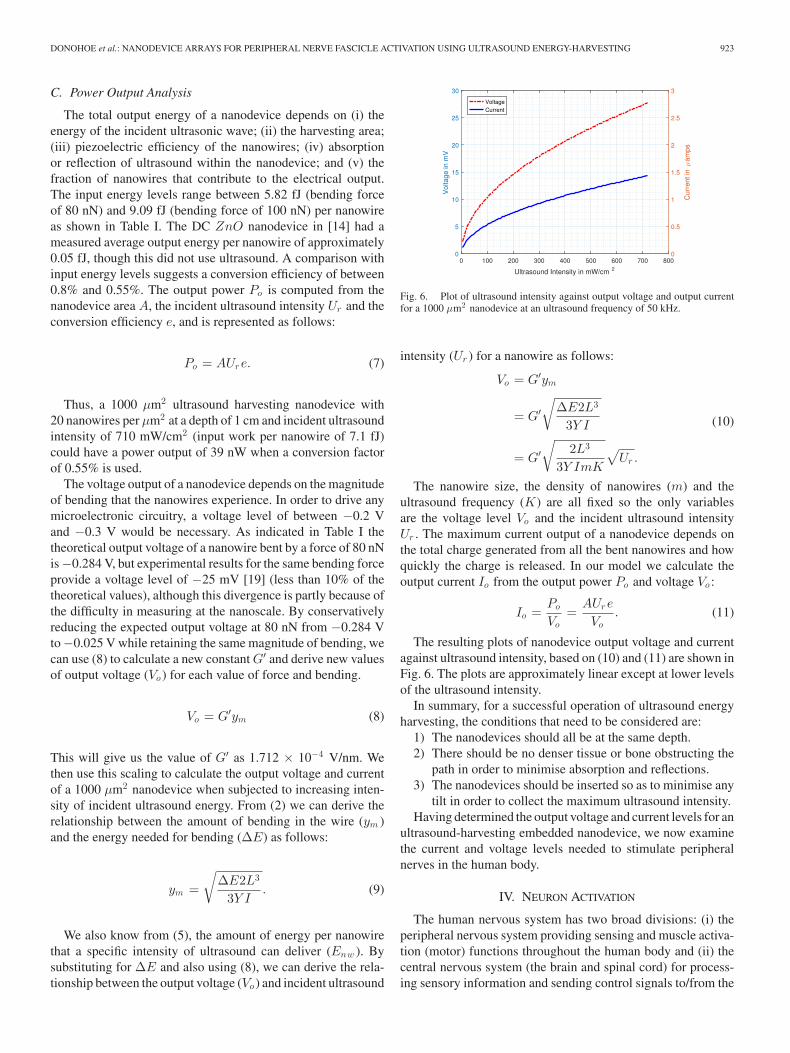
Fig. 6. Plot of ultrasound intensity against output voltage and output currentfor a 1000 μm2 nanodevice at an ultrasound frequency of 50 kHz.
intensity (Ur ) for a nanowire as follows:
Vo = G′ym
= G′√
ΔE2L3
3Y I
= G′√
2L3
3Y ImK
√Ur .
(10)
The nanowire size, the density of nanowires (m) and theultrasound frequency (K) are all fixed so the only variablesare the voltage level Vo and the incident ultrasound intensityUr . The maximum current output of a nanodevice depends onthe total charge generated from all the bent nanowires and howquickly the charge is released. In our model we calculate theoutput current Io from the output power Po and voltage Vo :
Io =Po
Vo=
AUre
Vo. (11)
The resulting plots of nanodevice output voltage and currentagainst ultrasound intensity, based on (10) and (11) are shown inFig. 6. The plots are approximately linear except at lower levelsof the ultrasound intensity.
In summary, for a successful operation of ultrasound energyharvesting, the conditions that need to be considered are:
1) The nanodevices should all be at the same depth.2) There should be no denser tissue or bone obstructing the
path in order to minimise absorption and reflections.3) The nanodevices should be inserted so as to minimise any
tilt in order to collect the maximum ultrasound intensity.Having determined the output voltage and current levels for an
ultrasound-harvesting embedded nanodevice, we now examinethe current and voltage levels needed to stimulate peripheralnerves in the human body.
IV. NEURON ACTIVATION
The human nervous system has two broad divisions: (i) theperipheral nervous system providing sensing and muscle activa-tion (motor) functions throughout the human body and (ii) thecentral nervous system (the brain and spinal cord) for process-ing sensory information and sending control signals to/from the
924 IEEE TRANSACTIONS ON NANOTECHNOLOGY, VOL. 16, NO. 6, NOVEMBER 2017
peripheral nervous system. The nervous system has two maintypes of cells: neurons for communications and glial cells forsupport and nutrition. Neurons have a resting potential, based onan ionic balance of sodium and potassium ions across the neuralmembrane, of approximately −70 mV. If a stimulus raises thispotential above −55 mV (e.g., by applying a pulse of magni-tude 15 mV or greater) then the neuron activates, where ionchannels in the membrane open and positively charged sodiumions flow across the membrane into the neuron (depolarisation).The potential rapidly increases to about 40 mV (a total increaseof 110 mV from rest). At this point the sodium ion channelsclose, potassium ion channels open and there’s a flow of posi-tive potassium ions out of the neuron (repolarisation) [20].
The electrical signal (action potential) then propagates downthe neuron’s axon and either transfers to another neuron (vianeurotransmitters) or a muscle cell, for example. The first neu-ron then returns to the rest state. The whole cycle takes between5 ms and 10 ms. A stimulus can be supplied as part of the normalfunctioning of the nervous system or as an externally inducedelectrical current. External pulses are usually supplied by ca-thodic stimulation where a negative electrode is placed outsidethe cell membrane. The negative potential outside the membraneinduces a current that reduces the trans-membrane voltage (de-polarises) and will trigger an action potential if the stimuluscurrent and the resulting change in membrane potential is largeenough.
The level of current needed to stimulate a neuron will dependon the excitability of the neuron, the electrode-neuron distanceand the pulse duration. Larger diameter axons are more excitableand require lower stimulus energy than smaller diameters. Suchlarger axons have an insulating sheath of myelin and are classedas Aα, Aβ and Aδ. The myelin sheath has regular gaps atintervals of 1 mm, called nodes of Ranvier (typical width of2 μm) where the action potential is regenerated. These nodesare also the points at which an external stimulus pulse will enterthe neuron.
The electrode voltage and the associated source current areimportant input values needed in order to determine the resul-tant currents and voltages induced in the neuron. Numerousresearch works have modeled the excitation of neurons usingmonopolar electrodes [21]–[23]. In particular, we are interestedin determining the magnitude of a stimulus current that trig-gers an action potential, the electrode voltage needed to drivethat current and the electrode position. This will allow us todetermine the appropriate current and voltage required from thenanodevices to stimulate the neurons in the nerve. The calcu-lation of stimulus current values using experimentally derivedempirical equations is described in the next section.
A. Activation Parameters
The effect of the stimulus can be varied by increasing or de-creasing the pulse length and hence influencing the activation ofneurons of different size and depth in the nerve bundle. The low-est possible stimulus current of an axon is called the rheobasebut this implies an infinitely long pulse [24]. The rheobase isusually measured at the source electrode. Due to the tissue
TABLE IIAXON CHARACTERISTICS
Axon Type Myelin Diameter Speed Chronaxie(μm) (m/s) (μs)
Aα Yes 13–20 80–120 50–100Aβ Yes 6–12 35–75 120Aδ Yes 1–5 10–35 170B Yes 3 3–15 200C No 0.2–1.5 0.5–2.0 400
resistivity, the rheobase will be higher when the electrode isplaced at a certain distance (e.g., on the skin). A more usualparameter is the chronaxie, the minimum time required for astimulus current that’s twice the value of the rheobase to stim-ulate a neuron [24]. Factors affecting the accuracy of chronaxiemeasurements are discussed by Geddes [25] who notes that themost reliable values are obtained when a square stimulus pulseis used. Axon characteristics, including their chronaxie valuefor different types of neurons are summarised in Table II.
The source current intensity for stimulation must be increasedas the distance between the electrode and the neuron increases.The increase in source current intensity with distance is definedby the current-distance equation [24], which is represented as:
Id = Ith + kd2 . (12)
The minimum threshold current for neuron activation at zerodistance is Ith . At a distance d, the activation current intensityis Id and the current-distance constant is k which is specific fordifferent types of axon. Values of k were analysed by Ranck[26] for a wide range of axon types and measured by varyingmethods. A more accurate method of determining the value fora peripheral motor neuron was devised by Mahman et al. [27]who also calculated a value for the threshold current Ith . In ourmodelling we use this calculated current-distance constant k of27 μA/mm2 .
The pulse duration and the corresponding threshold pulsecurrent intensity for neural activation can be plotted using theLapicque equation [24], which is represented as:
Ith = Ir
(1 +
C
t
)(13)
where the pulse duration is t, the rheobase current is Ir and thechronaxie is C. The shorter the pulse duration, the higher thethreshold intensity needed to activate a neuron. The optimumpulse duration for a specific neuron is the chronaxie. A plotof pulse duration against current intensity (Ith ), based on (13),for a myelinated and unmyelinated axon is shown in Fig. 7.For an electrode in very close proximity to a nerve we model arheobase current of 25 μA that’s derived from Mahman’s valueof threshold current (50 μA) and a pulse length of 100 μs.
If we consider a pulse length of 100 μs then we can seefrom Fig. 7 that the different axon types could be activated by astimulus current of less than 0.2 mA.
The magnitude of the stimulus current will also depend on thevoltage at the electrode. For a monopolar electrode the electricalpotential field Vu at a distance u is given by the following

DONOHOE et al.: NANODEVICE ARRAYS FOR PERIPHERAL NERVE FASCICLE ACTIVATION USING ULTRASOUND ENERGY-HARVESTING 925
Fig. 7. Plot of current against pulse duration for two types of axon, onemyelinated (Aα axon) and one unmyelinated (C axon). The current intensityfor a pulse duration of 100 μs is less than 0.2 mA.
Fig. 8. Plot of stimulus current and source voltage for a range of neuron dis-tances and a chronaxie of 100 μs. The further the neuron is from the nanodevicearray electrode the higher will be the required stimulus voltage/current.
equation [24]:
Vu =Id
4πρu. (14)
The stimulus current intensity is Id while the conductivity ofthe extracellular tissue is ρ. If we assume a homogenous tissuethen we can assign a specific value to the conductivity. A typicalvalue for neuronal tissue conductivity is 0.3 S/m [28]. The po-tential at zero distance is infinite so some specific radius has to beassigned to the electrode in order to provide a minimum valueof u and allow for a realistic source voltage [29]. Therefore,due to this factor we assign a radius of 0.1 mm. Fig. 8 showsthe variation in stimulus current and source electrode voltagewith neuron depth for a neuron with a chronaxie of 100 μsstimulated by a 100 μs pulse.
Values for electrode voltage and stimulus current, derivedfrom (12) and (14) for a range of neuron depths are shownin Table III. These values are comparable to experimental andmodelling results for cuff electrode stimulation of peripheralnerves [30].
The optimum position for a stimulating electrode is at a nodeof Ranvier but it is possible to trigger an action potential betweennodes if the stimulus is strong enough. The stimulus current andcorresponding electrode voltage are the key parameters that our
TABLE IIIELECTRODE VOLTAGE AND STIMULUS CURRENT FOR A RANGE OF NEURON
DEPTHS
Neuron Depth Electrode Voltage Stimulus Current(mm) (mV) (mA)
0.5 150.5 0.0571 204 0.0771.5 293 0.112 419 0.1582.5 580 0.2193 777 0.293
Fig. 9. Schematic diagram of median nerve fascicles at the wrist (A) and theelbow (B), showing how electrode placement can concentrate the stimulatingcurrent on groups of motor fascicles.
energy-harvesting nanodevices must provide in order to stimu-late neurons at different depths. We now examine the propertiesof specific peripheral nerves that we wish to stimulate.
B. Peripheral Nerve Bundles
Peripheral nerves have neurons grouped in bundles (fascicles)within a nerve and so it is difficult to trigger a specific neuron.
The peripheral nerves of the wrist and forearm that controlarm and hand movements are the radial, median and ulnar. Atthe wrist and elbow, these nerves are buried beneath a layerof skin/fat (between 1 cm and 1.5 cm) and hence are easilyaccessed [31]. The cross-sectional areas of the nerves vary be-tween 5 mm2 and 10 mm2 [32]. There has been some research inmapping the topography of fascicles through the median, radialand ulnar nerves by Jabaley et al. [33] and Stewart [34]. Thesestudies showed (i) the position of a fascicle could change withina nerve particularly after the nerve had branched and (ii) thatkey fascicles contained neurons of one type only (either motoror sensory). An accurate mapping of motor neurons to fascicleswould provide valuable information for the placement of thenanodevices and the calculation of the probability of stimulat-ing a particular neural response. A distribution of motor andsensory fascicles in the median nerve, based on [33] and [34],is shown in Fig. 9.

926 IEEE TRANSACTIONS ON NANOTECHNOLOGY, VOL. 16, NO. 6, NOVEMBER 2017
We model the median nerve as having an elliptical cross-section with a major diameter of 6 mm, a minor diameter of2 mm, a cross-sectional area of 9.5 mm2 and a perimeter of13.4 mm. If a stimulating electrode is placed at the mid-pointon the top surface of such a nerve then the radial distance fromthis point to the relevant fascicle will determine the level ofstimulating current needed. However, if the motor fascicles areconcentrated on one side of the nerve then the electrode shouldbe placed on that side of the nerve to avoid stimulating othersensory fascicles. Examples of electrode placement on the me-dian nerve at the wrist and elbow are shown in Fig. 9. In bothcases the electrodes are placed to maximise access to the mo-tor neuron fascicles and the stimulating current can be set topenetrate to the radial distances shown.
C. Nanodevice Neural Activation
A neuron’s axon can be stimulated at any point along itslength by an electrical pulse of sufficient magnitude. An acti-vating nanodevice must (i) have sufficient voltage and chargefor stimulation and (ii) allow for an interval of 10 ms betweendischarges. In theory, a neuron could be activated 100 times persecond but this would be considered a very high rate. Activationrates of 10 or less per second are more usual. Nerve stimuluscurrents are usually in the mA range (see Fig. 8), though thecloser the stimulating electrode can be placed to the nerve thenthe lower the requirement. Our modelled nanodevices have amaximum voltage level of tens of mV and produce current inthe μA range (see Fig. 6). Therefore, based on these require-ments, the nanodevices must be coupled together in parallel toincrease the current and in series to increase the voltage. Thecoupling of individual ultrasound harvesting nanodevices in se-ries to boost voltage output and in series to boost current outputis described by Wang in [19]. The experimental results show thatthe voltages and currents add as a linear superposition when theultrasound is activated. The nanodevices should be capable ofdelivering square-wave pulses of varying duration across twoelectrodes, a cathode of coupled zigzag electrodes and an anodeof coupled substrates, that can in turn stimulate a nerve.
The minimum possible pulse length from a nanodevice drivenby a 50 kHz ultrasound signal is 20 μs. A longer stimulationtime will contain a train of such pulses. The in-built rectifica-tion and capacitive properties of the nanogenerator convert thistrain to a single square-wave DC pulse. Neural stimulation sys-tems usually provide some form of charge balancing, deliveringa biphasic pulse of cathodic current followed by anodic cur-rent. The claimed benefit is to minimize the degrading effectsof charge build-up on the electrode and surrounding tissue. Oursystem is a passive device array and can only provide monopha-sic cathodic pulses. It cannot switch to biphasic operation orproduce more complex stimulation patterns.
The method of inserting nanodevices in close proximity toneurons then becomes an important factor. We propose en-casing an array of coupled nanodevices within a sealed patchof synthetic tissue, as illustrated in Fig. 10, and then insert-ing the patch of tissue at the site. The use of coupled ar-rays and bio-compatible packaging ensures that the individual
Fig. 10. Schematic diagram of coupled nanodevices embedded in a patch ofsynthetic biocompatible tissue.
nanodevices do not interact with the nerve or nerve fasciclebut only act through a single cathode/anode system. The bio-compatible material provides insulation for the array in thesurrounding conductive environment.
D. Patch Dimensions
The nanodevice array must deliver a current intensity (Id ) inaccordance to (12). That intensity in turn is also dependent onthe pulse duration as shown in (13). If the output current levelof a nanodevice at a particular ultrasound intensity is Io , and thethreshold stimulus current for a particular neuron depth is Id ,then the number of rows of coupled nanodevices to generate thethreshold current is:
Nr =Id
Io. (15)
The voltage must also be in the range specified by (14) andcalculated for an electrode radius of 0.1 mm. If the output voltageof a nanodevice at particular ultrasound intensity is Vo , and theelectrode voltage for a particular threshold current is Ve , thenthe number of columns of coupled nanodevices to generate thethreshold voltage is:
Nc =Ve
Vo. (16)
The median and ulnar nerves are contained in a skin/fatdepth between 1 cm and 1.5 cm. The external ultrasoundintensity will have dropped below its initial intensity of720 mW/cm2 at these depths. Hence we use a maximum in-tensity of 710 mW/cm2 with a maximum current and voltageper nanodevice of 1.42 μA and 27.5 mV. The minimum possi-ble area of a patch of nanodevices, Ap will be derived from thenumber of rows Nr , the number of columns Nc and the area ofone nanodevice an :
Ap = NrNcan . (17)
The basic length and width of an array of nanodevicesare set by the number of rows and columns. Our nanodevices are1000 μm2 and can be modelled as squares of side 32 μm. Therewill be a need to allow for small variations in dimension aswell as a space for coupling connections between the devices.We, therefore, increase the effective size of a nanodevice to40 μm per side, giving an effective area of 1600 μm2 . A plotof minimum array area for a range of neuron depths, pulse du-rations and input ultrasound intensity is shown in Fig. 11. Theplots show how the area increases for greater stimulus depth andshorter pulse lengths, since both of these will result in higher
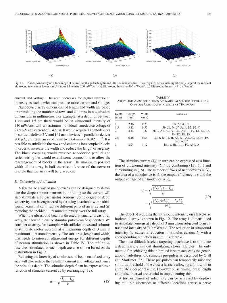
DONOHOE et al.: NANODEVICE ARRAYS FOR PERIPHERAL NERVE FASCICLE ACTIVATION USING ULTRASOUND ENERGY-HARVESTING 927
Fig. 11. Nanodevice array area for a range of neuron depths, pulse lengths and ultrasound intensities. The array area needs to be significantly larger if the incidentultrasound intensity is lower. (a) Ultrasound Intensity 200 mW/cm2 . (b) Ultrasound Intensity 400 mW/cm2 . (c) Ultrasound Intensity 710 mW/cm2 .
current and voltage. The area decreases for higher ultrasoundintensity as each device can produce more current and voltage.
Nanodevice array dimensions of length and width are basedon translating the number of rows and columns into equivalentdimensions in millimetres. For example, at a depth of between1 cm and 1.5 cm there would be an ultrasound intensity of710 mW/cm2 with a maximum individual nanodevice voltage of27.5 mV and current of 1.42 μA. It would require 73 nanodevicesin series to deliver 2 V and 141 nanodevices in parallel to deliver200 μA, giving an array of 3 mm by 5.64 mm or 16.92 mm2 . It ispossible to subdivide the rows and columns into coupled blocksin order to increase the width and reduce the length of an array.The block coupling would preserve nanodevice parallel andseries wiring but would extend some connections to allow therearrangement of blocks in the array. The maximum possiblewidth of the array is half the circumference of the nerve orfascicle that the array will be placed on.
E. Selectivity of Activation
A fixed-size array of nanodevices can be designed to stimu-late the deepest motor neurons but in doing so the current willalso stimulate all closer motor neurons. Some degree of depthselectivity can be engineered by (i) using a variable-width ultra-sound beam that can irradiate different parts of an array and (ii)reducing the incident ultrasound intensity over the full array.
When the ultrasound beam is directed at smaller areas of anarray, then lower intensity stimulus pulses can be generated. Weconsider an array, for example, with sufficient rows and columnsto stimulate motor neurons at a maximum depth of 3 mm atmaximum ultrasound intensity. The sub- area (length and width)that needs to intercept ultrasound energy for different depthsof neuron stimulation is shown in Table IV. The additionalfascicles stimulated at each depth are also shown based on thedistribution in Fig. 9.
Reducing the intensity of an ultrasound beam on a fixed arraysize will also reduce the resultant current and voltage and hencethe stimulus depth. The stimulus depth d can be expressed as afunction of stimulus current Id by rearranging (12).
d =
√Id − Ith
k(18)
TABLE IVARRAY DIMENSIONS FOR NEURON ACTIVATION AT SPECIFIC DEPTHS AND A
CONSTANT ULTRASOUND INTENSITY OF 710 MW/CM2
Depth Length Width Fascicles(mm) (mm) (mm)
1 2.16 0.28 5a, 5c, 4, B11.5 3.12 0.55 5b, 5d, 5e, 5f, 5g, 4, B2, B3, C2 4.44 0.6 5h, 3, A1, A2, A3, A4, A5, F1, F2, E1, E2, E3,
E4, E5, E8, E92.5 6.16 0.84 1a,1b, 1c, 1d, 1f, A6, A7, A8, A9, F3, F4, F5,
F6, E6, E73 8.24 1.12 1e, 1g, 1h, 1i, 1j, F7, A10, D
The stimulus current (Id ) in turn can be expressed as a func-tion of ultrasound intensity (Ur ) by combining (15), (11) andsubstituting in (18). The number of rows of nanodevices is Nr ,the area of a nanodevice is A, the output efficiency is e and theoutput voltage of a nanodevice is Vo .
d =
√(NrIo) − Ith
k
=
√(NrAeUr ) − IthVo
kVo.
(19)
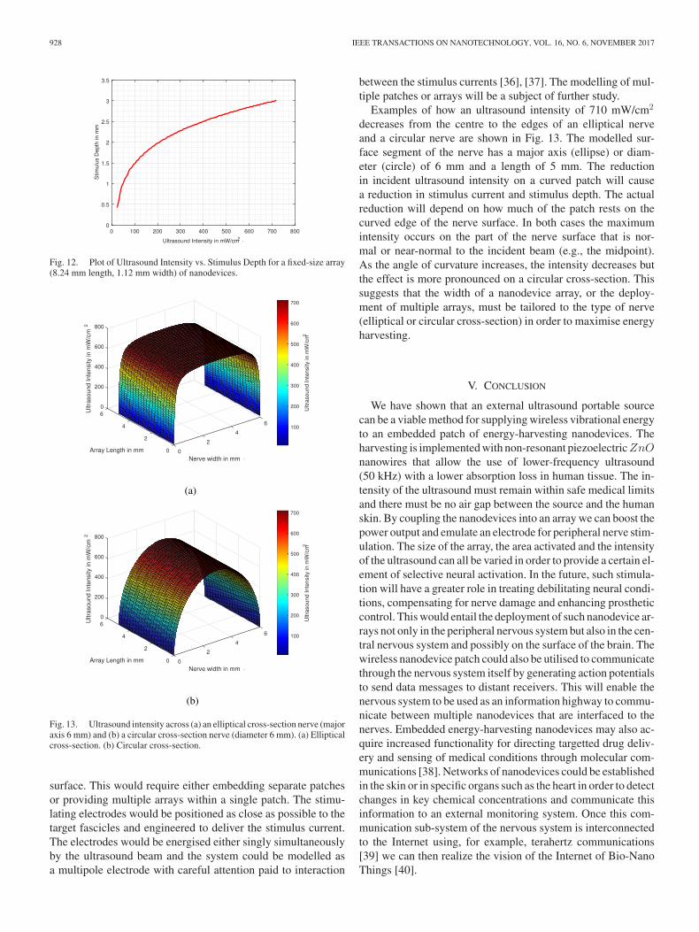
The effect of reducing the ultrasound intensity on a fixed-sizehorizontal array is shown in Fig. 12. The array is dimensionedto stimulate neurons at a depth of 3 mm when subjected to an ul-trasound intensity of 710 mW/cm2 . The reduction in ultrasoundintensity Ur causes a reduction in stimulus current Id with acorresponding reduction in stimulus depth d.
The most difficult fascicle targeting to achieve is to stimulatea deep fascicle without stimulating closer fascicles. The onlymethod for achieving this in limited circumstances is the gener-ation of sub-threshold stimulus pre-pulses as described by Grilland Mortimer [35]. These pre-pulses can temporarily raise thestimulus threshold of the closest fascicle allowing a follow-on tostimulate a deeper fascicle. However pulse timing, pulse lengthand pulse interval are crucial in implementing this.
A further degree of selectivity can be achieved by deploy-ing multiple electrodes at different locations across a nerve
928 IEEE TRANSACTIONS ON NANOTECHNOLOGY, VOL. 16, NO. 6, NOVEMBER 2017
Fig. 12. Plot of Ultrasound Intensity vs. Stimulus Depth for a fixed-size array(8.24 mm length, 1.12 mm width) of nanodevices.
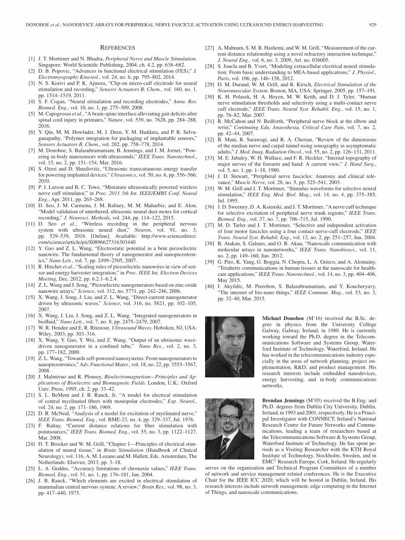
Fig. 13. Ultrasound intensity across (a) an elliptical cross-section nerve (majoraxis 6 mm) and (b) a circular cross-section nerve (diameter 6 mm). (a) Ellipticalcross-section. (b) Circular cross-section.
surface. This would require either embedding separate patchesor providing multiple arrays within a single patch. The stimu-lating electrodes would be positioned as close as possible to thetarget fascicles and engineered to deliver the stimulus current.The electrodes would be energised either singly simultaneouslyby the ultrasound beam and the system could be modelled asa multipole electrode with careful attention paid to interaction
between the stimulus currents [36], [37]. The modelling of mul-tiple patches or arrays will be a subject of further study.
Examples of how an ultrasound intensity of 710 mW/cm2
decreases from the centre to the edges of an elliptical nerveand a circular nerve are shown in Fig. 13. The modelled sur-face segment of the nerve has a major axis (ellipse) or diam-eter (circle) of 6 mm and a length of 5 mm. The reductionin incident ultrasound intensity on a curved patch will causea reduction in stimulus current and stimulus depth. The actualreduction will depend on how much of the patch rests on thecurved edge of the nerve surface. In both cases the maximumintensity occurs on the part of the nerve surface that is nor-mal or near-normal to the incident beam (e.g., the midpoint).As the angle of curvature increases, the intensity decreases butthe effect is more pronounced on a circular cross-section. Thissuggests that the width of a nanodevice array, or the deploy-ment of multiple arrays, must be tailored to the type of nerve(elliptical or circular cross-section) in order to maximise energyharvesting.
V. CONCLUSION
We have shown that an external ultrasound portable sourcecan be a viable method for supplying wireless vibrational energyto an embedded patch of energy-harvesting nanodevices. Theharvesting is implemented with non-resonant piezoelectric ZnOnanowires that allow the use of lower-frequency ultrasound(50 kHz) with a lower absorption loss in human tissue. The in-tensity of the ultrasound must remain within safe medical limitsand there must be no air gap between the source and the humanskin. By coupling the nanodevices into an array we can boost thepower output and emulate an electrode for peripheral nerve stim-ulation. The size of the array, the area activated and the intensityof the ultrasound can all be varied in order to provide a certain el-ement of selective neural activation. In the future, such stimula-tion will have a greater role in treating debilitating neural condi-tions, compensating for nerve damage and enhancing prostheticcontrol. This would entail the deployment of such nanodevice ar-rays not only in the peripheral nervous system but also in the cen-tral nervous system and possibly on the surface of the brain. Thewireless nanodevice patch could also be utilised to communicatethrough the nervous system itself by generating action potentialsto send data messages to distant receivers. This will enable thenervous system to be used as an information highway to commu-nicate between multiple nanodevices that are interfaced to thenerves. Embedded energy-harvesting nanodevices may also ac-quire increased functionality for directing targetted drug deliv-ery and sensing of medical conditions through molecular com-munications [38]. Networks of nanodevices could be establishedin the skin or in specific organs such as the heart in order to detectchanges in key chemical concentrations and communicate thisinformation to an external monitoring system. Once this com-munication sub-system of the nervous system is interconnectedto the Internet using, for example, terahertz communications[39] we can then realize the vision of the Internet of Bio-NanoThings [40].
DONOHOE et al.: NANODEVICE ARRAYS FOR PERIPHERAL NERVE FASCICLE ACTIVATION USING ULTRASOUND ENERGY-HARVESTING 929
REFERENCES
[1] J. T. Mortimer and N. Bhadra, Peripheral Nerve and Muscle Stimulation.Singapore: World Scientific Publishing, 2004, ch. 4.2, pp. 638–682.
[2] D. B. Popovic, “Advances in functional electrical stimulation (FES),” J.Electromyography Kinesiol., vol. 24, no. 6, pp. 795–802, 2014.
[3] N. S. Korivi and P. K. Ajmera, “Clip-on micro-cuff electrode for neuralstimulation and recording,” Sensors Actuators B, Chem., vol. 160, no. 1,pp. 1514–1519, 2011.
[4] S. F. Cogan, “Neural stimulation and recording electrodes,” Annu. Rev.Biomed. Eng., vol. 10, no. 1, pp. 275–309, 2008.
[5] M. Capogrosso et al., “A brain-spine interface alleviating gait deficits afterspinal cord injury in primates,” Nature, vol. 539, no. 7628, pp. 284–288,2016.
[6] Y. Qin, M. M. Howlader, M. J. Deen, Y. M. Haddara, and P. R. Selva-ganapathy, “Polymer integration for packaging of implantable sensors,”Sensors Actuators B, Chem., vol. 202, pp. 758–778, 2014.
[7] M. Donohoe, S. Balasubramaniam, B. Jennings, and J. M. Jornet, “Pow-ering in-body nanosensors with ultrasounds,” IEEE Trans. Nanotechnol.,vol. 15, no. 2, pp. 151–154, Mar. 2016.
[8] S. Ozeri and D. Shmilovitz, “Ultrasonic transcutaneous energy transferfor powering implanted devices,” Ultrasonics, vol. 50, no. 6, pp. 556–566,2010.
[9] P. J. Larson and B. C. Towe, “Miniature ultrasonically powered wirelessnerve cuff stimulator,” in Proc. 2011 5th Int. IEEE/EMBS Conf. NeuralEng., Apr. 2011, pp. 265–268.
[10] D. Seo, J. M. Carmena, J. M. Rabaey, M. M. Maharbiz, and E. Alon,“Model validation of untethered, ultrasonic neural dust motes for corticalrecording,” J. Neurosci. Methods, vol. 244, pp. 114–122, 2015.
[11] D. Seo et al., “Wireless recording in the peripheral nervoussystem with ultrasonic neural dust,” Neuron, vol. 91, no. 3,pp. 529–539, 2016. [Online]. Available: http://www.sciencedirect.com/science/article/pii/S0896627316303440
[12] Y. Gao and Z. L. Wang, “Electrostatic potential in a bent piezoelectricnanowire. The fundamental theory of nanogenerator and nanopiezotron-ics,” Nano Lett., vol. 7, pp. 2499–2505, 2007.
[13] R. Hinchet et al., “Scaling rules of piezoelectric nanowires in view of sen-sor and energy harvester integration,” in Proc. IEEE Int. Electron DevicesMeeting, Dec. 2012, pp. 6.2.1–6.2.4.
[14] Z. L. Wang and J. Song, “Piezoelectric nanogenerators based on zinc oxidenanowire arrays,” Science, vol. 312, no. 5771, pp. 242–246, 2006.
[15] X. Wang, J. Song, J. Liu, and Z. L. Wang, “Direct-current nanogeneratordriven by ultrasonic waves,” Science, vol. 316, no. 5821, pp. 102–105,2007.
[16] X. Wang, J. Liu, J. Song, and Z. L. Wang, “Integrated nanogenerators inbiofluid,” Nano Lett., vol. 7, no. 8, pp. 2475–2479, 2007.
[17] W. R. Hendee and E. R. Ritenour, Ultrasound Waves. Hoboken, NJ, USA:Wiley, 2003, pp. 303–316.
[18] X. Wang, Y. Gao, Y. Wei, and Z. Wang, “Output of an ultrasonic wave-driven nanogenerator in a confined tube,” Nano Res., vol. 2, no. 3,pp. 177–182, 2009.
[19] Z. L. Wang, “Towards self-powered nanosystems: From nanogenerators tonanopiezotronics,” Adv. Functional Mater., vol. 18, no. 22, pp. 3553–3567,2008.
[20] J. Malmivuo and R. Plonsey, Bioelectromagnetism—Principles and Ap-plications of Bioelectric and Biomagnetic Fields. London, U.K.: OxfordUniv. Press, 1995, ch. 2, pp. 33–42.
[21] S. L. BeMent and J. B. Ranck, Jr, “A model for electrcal stimulationof central myelinated fibers with monopolar electrodes,” Exp. Neurol.,vol. 24, no. 2, pp. 171–186, 1969.
[22] D. R. McNeal, “Analysis of a model for excitation of myelinated nerve,”IEEE Trans. Biomed. Eng., vol. BME-23, no. 4, pp. 329–337, Jul. 1976.
[23] F. Rattay, “Current distance relations for fiber stimulation withpointsources,” IEEE Trans. Biomed. Eng., vol. 55, no. 3, pp. 1122–1127,Mar. 2008.
[24] D. T. Brocker and W. M. Grill, “Chapter 1—Principles of electrical stim-ulation of neural tissue,” in Brain Stimulation (Handbook of ClinicalNeurology), vol. 116, A. M. Lozano and M. Hallett, Eds. Amsterdam, TheNetherlands: Elsevier, 2013, pp. 3–18.
[25] L. A. Geddes, “Accuracy limitations of chronaxie values,” IEEE Trans.Biomed. Eng., vol. 51, no. 1, pp. 176–181, Jan. 2004.
[26] J. B. Ranck, “Which elements are excited in electrical stimulation ofmammalian central nervous system: A review,” Brain Res., vol. 98, no. 3,pp. 417–440, 1975.
[27] A. Mahnam, S. M. R. Hashemi, and W. M. Grill, “Measurement of the cur-rent distance relationship using a novel refractory interaction technique,”J. Neural Eng., vol. 6, no. 3, 2009, Art. no. 036005.
[28] S. Joucla and B. Yvert, “Modeling extracellular electrical neural stimula-tion: From basic understanding to MEA-based applications,” J. Physiol.,Paris, vol. 106, pp. 146–158, 2012.
[29] D. M. Durand, W. M. Grill, and R. Kirsch, Electrical Stimulation of theNeuromuscular System. Boston, MA, USA: Springer, 2005, pp. 157–191.
[30] K. H. Polasek, H. A. Hoyen, M. W. Keith, and D. J. Tyler, “Humannerve stimulation thresholds and selectivity using a multi-contact nervecuff electrode,” IEEE Trans. Neural Syst. Rehabil. Eng., vol. 15, no. 1,pp. 76–82, Mar. 2007.
[31] R. McCahon and N. Bedforth, “Peripheral nerve block at the elbow andwrist,” Continuing Edu. Anaesthesia, Critical Care Pain, vol. 7, no. 2,pp. 42–44, 2007.
[32] B. Mani, R. Sarawagi, and R. A. Cherian, “Review of the dimensionsof the median nerve and carpal tunnel using sonography in asymptomaticadults,” J. Med. Imag. Radiation Oncol., vol. 55, no. 2, pp. 126–131, 2011.
[33] M. E. Jabaley, W. H. Wallace, and F. R. Heckler, “Internal topography ofmajor nerves of the forearm and hand: A current view,” J. Hand Surg.,vol. 5, no. 1, pp. 1–18, 1980.
[34] J. D. Stewart, “Peripheral nerve fascicles: Anatomy and clinical rele-vance,” Muscle Nerve, vol. 28, no. 5, pp. 525–541, 2003.
[35] W. M. Grill and J. T. Mortimer, “Stimulus waveforms for selective neuralstimulation,” IEEE Eng. Med. Biol. Mag., vol. 14, no. 4, pp. 375–385,Jul. 1995.
[36] J. D. Sweeney, D. A. Ksienski, and J. T. Mortimer, “A nerve cuff techniquefor selective excitation of peripheral nerve trunk regions,” IEEE Trans.Biomed. Eng., vol. 37, no. 7, pp. 706–715, Jul. 1990.
[37] M. D. Tarler and J. T. Mortimer, “Selective and independent activationof four motor fascicles using a four contact nerve-cuff electrode,” IEEETrans. Neural Syst. Rehabil. Eng., vol. 12, no. 2, pp. 251–257, Jun. 2004.
[38] B. Atakan, S. Galmes, and O. B. Akan, “Nanoscale communication withmolecular arrays in nanonetworks,” IEEE Trans. Nanobiosci., vol. 11,no. 2, pp. 149–160, Jun. 2012.
[39] G. Piro, K. Yang, G. Boggia, N. Chopra, L. A. Grieco, and A. Alomainy,“Terahertz communications in human tissues at the nanoscale for health-care applications,” IEEE Trans. Nanotechnol., vol. 14, no. 3, pp. 404–406,May 2015.
[40] I. Akyildiz, M. Pierobon, S. Balasubramaniam, and Y. Koucheryavy,“The internet of bio-nano things,” IEEE Commun. Mag., vol. 53, no. 3,pp. 32–40, Mar. 2015.
Michael Donohoe (M’16) received the B.Sc. de-gree in physics from the University CollegeGalway, Galway, Ireland, in 1980. He is currentlyworking toward the Ph.D. degree in the Telecom-munications Software and Systems Group, Water-ford Institute of Technology, Waterford, Ireland. Hehas worked in the telecommunications industry espe-cially in the areas of network planning, project im-plementation, R&D, and product management. Hisresearch interests include embedded nanodevices,energy harvesting, and in-body communicationsnetworks.
Brendan Jennings (M’05) received the B.Eng. andPh.D. degrees from Dublin City University, Dublin,Ireland, in 1993 and 2001, respectively. He is a Princi-pal Investigator with CONNECT, Ireland’s NationalResearch Centre for Future Networks and Commu-nications, leading a team of researchers based atthe Telecommunications Software & Systems Group,Waterford Institute of Technology. He has spent pe-riods as a Visiting Researcher with the KTH RoyalInstitute of Technology, Stockholm, Sweden, and inEMC2 Research Europe, Cork, Ireland. He regularly
serves on the organization and Technical Program Committees of a numberof network and service management related conferences. He is the ExecutiveChair for the IEEE ICC 2020, which will be hosted in Dublin, Ireland. Hisresearch interests include network management, edge computing in the Internetof Things, and nanoscale communications.
930 IEEE TRANSACTIONS ON NANOTECHNOLOGY, VOL. 16, NO. 6, NOVEMBER 2017
Josep Miquel Jornet (M’13) received the B.S. de-gree in telecommunication engineering, the M.Sc.degree in information and communication technolo-gies from the Universitat Politcnica de Catalunya,Barcelona, Spain, in 2008, and the Ph.D. degreein electrical and computer engineering from theGeorgia Institute of Technology (Georgia Tech), At-lanta, GA, USA, in 2013. He is currently an AssistantProfessor in the Department of Electrical Engineer-ing, University at Buffalo, The State University ofNew York, Buffalo, NY, USA. From September 2007
to December 2008, he was a Visiting Researcher in the Massachusetts Insti-tute of Technology (MIT), Cambridge, MA, USA, under the MIT Sea Grantprogram. His current research interests include Terahertz-band communicationnetworks, nanophotonic wireless communication, intrabody wireless nanosen-sor networks, and the Internet of Nano Things. He received the Oscar P. CleaverAward for outstanding graduate students in the School of Electrical and Com-puter Engineering, at Georgia Tech in 2009. He also received the BroadbandWireless Networking Lab Researcher of the Year Award in 2010. In 2016 and2017, he received the Distinguished TPC Member Award at the IEEE Interna-tional Conference on Computer Communications (INFOCOM). In 2017, he re-ceived the IEEE Communications Society Young Professional Best InnovationAward. Since July 2016, he is the Editor-in-Chief of the Nano Communica-tion Networks (Elsevier) Journal. He also serves in the Steering Committee ofthe ACM Nanoscale Computing and Communications Conference series since2016. He is a member the ACM.
Sasitharan Balasubramaniam (SM’14) receivedthe Bachelor’s degree in electrical and electronicengineering and the Ph.D. degree from the Univer-sity of Queensland, Brisbane, QLD, Australia, in1998 and 2005, respectively, and the Master’s degreein computer and communication engineering fromthe Queensland University of Technology, Brisbane,QLD, Australia, in 1999. He is currently an Academyof Finland Research Fellow in the Nano Com-munication Centre, Department of Electronic andCommunication Engineering, Tampere University of
Technology, Tampere, Finland, and the Acting Director of Research in theTelecommunication Software and Systems Group, Waterford Institute of Tech-nology, Waterford, Ireland, where he worked on a number of Science FoundationIreland projects. He has published more than 90 papers and actively participatesin a number of technical programme committee for various conferences. Hewas the TPC Co-Chair for ACM NANOCOM 2014 and General Chair in 2015which he co-founded. He is currently an editor for the IEEE INTERNET OF
THINGS JOURNAL, Elsevier Nano Communication Networks, and Elsevier Digi-tal Communication Networks. His current research interests includes bioinspiredcommunication networks, as well as molecular communications.