ieee transactions on nanotechnology, vol. … · ieee transactions on nanotechnology, vol. 13, ......
TRANSCRIPT
IEEE TRANSACTIONS ON NANOTECHNOLOGY, VOL. 13, NO. 1, JANUARY 2014 123
Impact of the Substrate Material on the RFPerformance of Carbon-Nanotube Transistors
Sabbir Ahmed, Navid Paydavosi, Ahsan UI Alam, Kyle David Holland, Diego Kienle,and Mani Vaidyanathan, Member, IEEE
Abstract—We examine the effect of the substrate material onthe radio-frequency (RF) behavior of carbon-nanotube transis-tors by considering the impact of substrate polar phonons (SPPs).We consider SPP scattering from AlN, SiO2 , HfO2 , and ZrO2substrates within a semiclassical approach by solving the time-dependent Boltzmann transport equation self-consistently with thePoisson equation. Various RF figures of merit, such as the unity-current gain frequency fT , the unity-power-gain frequency fmax ,the transconductance gm , and the two-port y-parameters, are de-termined in order to characterize the impact of SPP scattering.We first consider the impact of SPP scattering on the RF behaviorof an intrinsic single-tube carbon nanotube field-effect transistor(CNFET). These single-tube results are then combined with theexternal parasitic elements to analyze the pitch-dependent, RF be-havior of an extrinsic array-based CNFET. It is shown that AlNsubstrates have the least impact in degrading the RF performanceof a CNFET, while the more polar substrates (HfO2 or ZrO2 )have a greater impact. This varying behavior can be attributed tothe SPP energies, which are higher in AlN compared to the othermaterials, making CNFETs with AlN substrates less susceptibleto SPP scattering even at room temperature. Our results suggestthat substrate engineering will become an important component inthe design process of emerging devices to achieve an optimized RFperformance.
Index Terms—Carbon nanotube (CN), RF CMOS, high-frequency behavior, phonon scattering, radio-frequency (RF) be-havior, substrate polar phonon (SPP), time-dependent transport,tube pitch, two-port parameters.
I. INTRODUCTION
S INCE their discovery in 1991, carbon nanotubes (CNs)have stimulated a plethora of experimental and theoretical
research to better understand the charge transport in (quasi) 1-D-material systems, and to assess whether CN-based channel
Manuscript received May 6, 2013; accepted October 15, 2013. Date of pub-lication December 11, 2013; date of current version January 6, 2014. Thiswork was supported by the Natural Sciences and Engineering Research Council(NSERC) of Canada, Queen Elizabeth II Graduate Scholarship, and AlbertaAdvanced Education & Technology. The review of this paper was arranged byAssociate Editor A. Ghosh.
S. Ahmed, A. U. Alam, K. D. Holland & M. Vaidyanathan are with theDepartment of Electrical and Computer Engineering, University of Alberta, Ed-monton, AB, Canada (e-mail: [email protected]).
N. Paydavosi is with the BSIM Group, University of California, Berkeley,CA 94720, USA.
D. Kienle is with the Theoretische Physik I, Universitat Bayreuth,D-Bayreuth, Germany.
Color versions of one or more of the figures in this paper are available onlineat http://ieeexplore.ieee.org.
Digital Object Identifier 10.1109/TNANO.2013.2294472
materials have the potential to replace or augment the well-matured, silicon-based CMOS technology [1].
One of the major concerns has been to understand how scatter-ing by lattice vibrations native to the nanotube (native phonons)affect the terminal behavior of CN field-effect transistors (CN-FETs). So far, most studies on native phonon scattering havebeen conducted for CNFETs under steady-state (dc) operatingconditions [2]–[9]; both measurements and simulations of the dcmobility and output currents have revealed that native acousticand optical phonons strongly contribute to limiting the transportin metallic and semiconducting tubes, including a saturation ofthe output current at high bias [2], [6], [10].
Another source of scattering (over and above that from na-tive phonons) originates from phonons within the substrate onwhich the tube resides, and this has received detailed attentiononly recently, when it was realized that transport in nanoscalechannels may be quite sensitive to the substrate type [11]–[13].Many of these substrates are polar in nature, so that the lat-tice vibrations of the substrate form oscillating bond dipolesthat generate polarization fields that die out exponentiallyfrom the surface [14]. In carbon-based materials, such as CNsand graphene, the distance between the atomically thin channeland the substrate is within 0.35 nm (Van-der Waals distance), andthe polarization fields can interact quite strongly with the chan-nel electrons, leading to the so-called “substrate polar phonon(SPP) scattering” [11]. It has been argued that beyond a temper-ature of T = 100 K, SPP scattering is activated and dominatesthe electronic transport, causing the dc mobility to degrade bya factor of 10 [15].
Regarding the radio-frequency (RF) behavior, recent studieshave shown that CNFETs have the potential to outperform otherhigh-frequency transistors, even in the presence of significantscattering from native acoustic and optical phonons [16]. How-ever, this outcome should be revisited, given that SPP scatteringhas been flagged as an additional major contributor to devicedegradation at ambient temperatures [15]. As far as we know,a detailed investigation of the importance of SPP scattering onthe RF performance of CNFETs has yet to be performed, eithertheoretically or experimentally.
In this paper, we investigate the impact of SPP scatteringon the high-frequency characteristics of array-based, CN tran-sistors at varying tube pitches. The RF performance is com-pared for four substrate materials: AlN, SiO2 , HfO2 , and ZrO2 .We show that SPP scattering substantially affects the device’sRF performance and, most importantly, displays a strong de-pendence on the choice of substrate. Among the materialsstudied, it is demonstrated that AlN degrades the device’s RF
1536-125X © 2013 IEEE. Personal use is permitted, but republication/redistribution requires IEEE permission.See http://www.ieee.org/publications standards/publications/rights/index.html for more information.
124 IEEE TRANSACTIONS ON NANOTECHNOLOGY, VOL. 13, NO. 1, JANUARY 2014
performance the least, which can be attributed to the high energyof the phonons in AlN in comparison to the other substrates. Thisresult is in accord with the qualitative expectation of Perebeinoset al. [15], who commented on the possible impact of differentpolar substrates on the dc mobility; in this paper, we focus on theRF performance, and we provide detailed quantitative results.
The simulation approach that allows us to extract the relevantRF figures of merit in the presence of various scattering sourcesconsists of two steps. First, a solver for the time-dependentBoltzmann transport equation (BTE) self-consistently coupledto the Poisson equation, developed in [10] using COMSOL [17],is employed to simulate the RF behavior of an intrinsic single-tube device at various widths (pitches) of the tube block. Thecollision integrals for the SPP scattering, based on the formalismof [15], are developed and included in the BTE along with thecollision integrals for the native acoustic and optical phonons.Second, the external parasitic resistances and capacitances arecombined with the results of the intrinsic single-tube block asdescribed in [16] to establish the extrinsic y-parameters of thearray-based structure; these allow the extraction of key extrinsichigh-frequency figures of merit, including the unity-current-gain frequency fT , the unity-power-gain frequency fmax , theunilateral power gain U , the maximum stable gain (MSG), andthe maximum available gain (MAG) [18].
This paper is organized as follows. Section II briefly sum-marizes the BTE-Poisson approach used to determine the RFtransport characteristics of a single-tube block, including thescattering due to native acoustic, native optical, and substratephonons; the details on the respective collision integrals are pro-vided in the Appendix. We then proceed to determine the intrin-sic high-frequency characteristics of a single-tube CNFET andto examine how these characteristics are impacted by the choiceof substrate. In Section III, a complete lumped circuit model isdeveloped for an overall array-based CNFET, that includes allparasitic elements, and we discuss how SPP scattering from dif-ferent substrates affects the transistor’s extrinsic RF figures ofmerit at various tube densities. The results of our investigationare summarized in Section IV.
II. INTRINSIC DEVICE
A. BTE-Poisson Approach
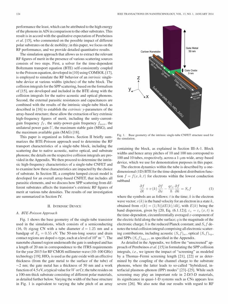
Fig. 1 shows the base geometry of the single-tube transistorused in the simulations, which consists of a semiconducting(16, 0) zigzag CN with a tube diameter d = 1.25 nm and abandgap of Eg = 0.55 eV. The 50-nm-long source and draincontact regions are doped n-type, each at a level of 109 m−1 . Thenanotube channel region underneath the gate is undoped and hasa length of 20 nm in correspondence to the ITRS requirementsfor the year 2015 for RF CMOS millimeter-wave (10–100 GHz)technology [19]; HfO2 is used as the gate oxide with an effectivethickness (from the gate metal to the surface of the tube) of∼2 nm; the gate metal has a thickness of 50 nm and a workfunction of 4.5 eV, a typical value for W or Cr; the tube resides ona 100-nm thick substrate consisting of different polar materials,as detailed further below. Varying the width of the base structurein Fig. 1 is equivalent to varying the tube pitch of an array
Fig. 1. Base geometry of the intrinsic single-tube CNFET structure used forthe simulation.
containing the block, as explained in Section III-A-1. Blockwidths and hence array pitches of 10 and 100 nm correspond to100 and 10 tubes, respectively, across a 1-μm-wide, array-baseddevice, which we use for demonstration purposes in this paper.
The electron dynamics within the tube is described by a one-dimensional (1D) BTE for the time-dependent distribution func-tion f = f(x, k, t) for electrons within the lowest conductionsubband
∂f
∂t+ v (k)
∂f
∂x− qεx
�
∂f
∂k= Sof (1)
where the symbols are as follows: t is the time; k is the electronwave vector; v(k) is the band velocity for an electron in a state k,obtained from v(k) = (1/�)[dE(k)/dk], with E(k) being theband dispersion, given by [20, Eq. (6.1.12)]; εx = εx (x, t) isthe time-dependent, circumferentially averaged x-component ofthe electric field along the tube surface; q is the magnitude of theelectronic charge; � is the reduced Planck constant; and Sof de-notes the total collision integral comprising all electronic scatter-ing contributions, including acoustic (Sof)ac , optical (Sof)op ,and SPPs (Sof)spp,ν , as specified in the Appendix.
As detailed in the Appendix, we follow the “unscreened” ap-proach of Perebeinos et al. [15] in formulating the SPP collisionintegrals, i.e., we ignore the impact of “screening” as modeledby a Thomas–Fermi screening length [21], [22] or as deter-mined by the coupling of the channel charge to the substratephonons, where the latter leads to so-called “hybridized, in-terfacial plasmon–phonon (IPP) modes” [23]–[25]. While suchscreening may play an important role in 2-D/3-D materials,its significance in quasi-1-D systems such as CNs appears lesssevere [26]. We also note that our results with regard to RF
AHMED et al.: IMPACT OF THE SUBSTRATE MATERIAL ON THE RF PERFORMANCE OF CARBON-NANOTUBE TRANSISTORS 125
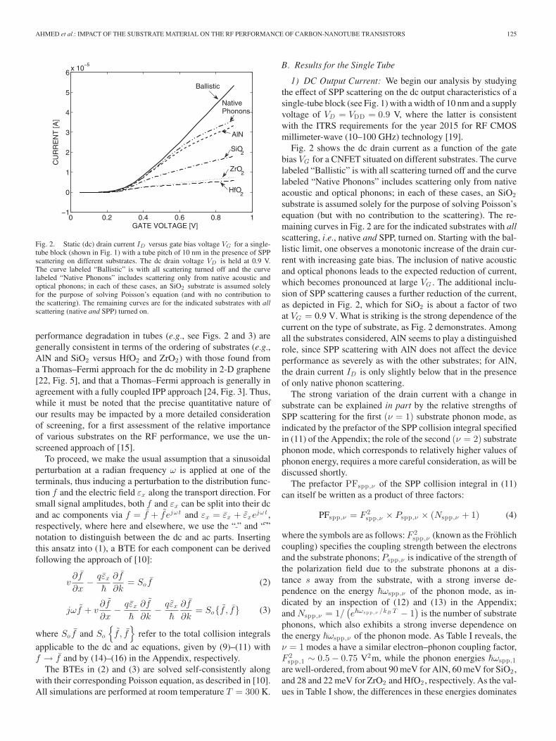
Fig. 2. Static (dc) drain current ID versus gate bias voltage VG for a single-tube block (shown in Fig. 1) with a tube pitch of 10 nm in the presence of SPPscattering on different substrates. The dc drain voltage VD is held at 0.9 V.The curve labeled “Ballistic” is with all scattering turned off and the curvelabeled “Native Phonons” includes scattering only from native acoustic andoptical phonons; in each of these cases, an SiO2 substrate is assumed solelyfor the purpose of solving Poisson’s equation (and with no contribution tothe scattering). The remaining curves are for the indicated substrates with allscattering (native and SPP) turned on.
performance degradation in tubes (e.g., see Figs. 2 and 3) aregenerally consistent in terms of the ordering of substrates (e.g.,AlN and SiO2 versus HfO2 and ZrO2) with those found froma Thomas–Fermi approach for the dc mobility in 2-D graphene[22, Fig. 5], and that a Thomas–Fermi approach is generally inagreement with a fully coupled IPP approach [24, Fig. 3]. Thus,while it must be noted that the precise quantitative nature ofour results may be impacted by a more detailed considerationof screening, for a first assessment of the relative importanceof various substrates on the RF performance, we use the un-screened approach of [15].
To proceed, we make the usual assumption that a sinusoidalperturbation at a radian frequency ω is applied at one of theterminals, thus inducing a perturbation to the distribution func-tion f and the electric field εx along the transport direction. Forsmall signal amplitudes, both f and εx can be split into their dcand ac components via f = f + f ejωt and εx = εx + εxejωt ,respectively, where here and elsewhere, we use the “ ” and “ ”notation to distinguish between the dc and ac parts. Insertingthis ansatz into (1), a BTE for each component can be derivedfollowing the approach of [10]:
v∂f
∂x− qεx
�
∂f
∂k= Sof (2)
jωf + v∂f
∂x− qεx
�
∂f
∂k− qεx
�
∂f
∂k= So{f , f} (3)
where Sof and So
{
f , f}
refer to the total collision integrals
applicable to the dc and ac equations, given by (9)–(11) withf → f and by (14)–(16) in the Appendix, respectively.
The BTEs in (2) and (3) are solved self-consistently alongwith their corresponding Poisson equation, as described in [10].All simulations are performed at room temperature T = 300 K.
B. Results for the Single Tube
1) DC Output Current: We begin our analysis by studyingthe effect of SPP scattering on the dc output characteristics of asingle-tube block (see Fig. 1) with a width of 10 nm and a supplyvoltage of VD = VDD = 0.9 V, where the latter is consistentwith the ITRS requirements for the year 2015 for RF CMOSmillimeter-wave (10–100 GHz) technology [19].
Fig. 2 shows the dc drain current as a function of the gatebias VG for a CNFET situated on different substrates. The curvelabeled “Ballistic” is with all scattering turned off and the curvelabeled “Native Phonons” includes scattering only from nativeacoustic and optical phonons; in each of these cases, an SiO2substrate is assumed solely for the purpose of solving Poisson’sequation (but with no contribution to the scattering). The re-maining curves in Fig. 2 are for the indicated substrates with allscattering, i.e., native and SPP, turned on. Starting with the bal-listic limit, one observes a monotonic increase of the drain cur-rent with increasing gate bias. The inclusion of native acousticand optical phonons leads to the expected reduction of current,which becomes pronounced at large VG . The additional inclu-sion of SPP scattering causes a further reduction of the current,as depicted in Fig. 2, which for SiO2 is about a factor of twoat VG = 0.9 V. What is striking is the strong dependence of thecurrent on the type of substrate, as Fig. 2 demonstrates. Amongall the substrates considered, AlN seems to play a distinguishedrole, since SPP scattering with AlN does not affect the deviceperformance as severely as with the other substrates; for AlN,the drain current ID is only slightly below that in the presenceof only native phonon scattering.
The strong variation of the drain current with a change insubstrate can be explained in part by the relative strengths ofSPP scattering for the first (ν = 1) substrate phonon mode, asindicated by the prefactor of the SPP collision integral specifiedin (11) of the Appendix; the role of the second (ν = 2) substratephonon mode, which corresponds to relatively higher values ofphonon energy, requires a more careful consideration, as will bediscussed shortly.
The prefactor PFspp,ν of the SPP collision integral in (11)can itself be written as a product of three factors:
PFspp,ν = F 2spp,ν × Pspp,ν × (Nspp,ν + 1) (4)
where the symbols are as follows: F 2spp,ν (known as the Frohlich
coupling) specifies the coupling strength between the electronsand the substrate phonons; Pspp,ν is indicative of the strength ofthe polarization field due to the substrate phonons at a dis-tance s away from the substrate, with a strong inverse de-pendence on the energy �ωspp,ν of the phonon mode, as in-dicated by an inspection of (12) and (13) in the Appendix;and Nspp,ν = 1/
(
e�ω s p p , ν /kB T − 1)
is the number of substratephonons, which also exhibits a strong inverse dependence onthe energy �ωspp,ν of the phonon mode. As Table I reveals, theν = 1 modes a have a similar electron–phonon coupling factor,F 2
spp,1 ∼ 0.5 − 0.75 V2m, while the phonon energies �ωspp,1are well-ordered, from about 90 meV for AlN, 60 meV for SiO2 ,and 28 and 22 meV for ZrO2 and HfO2 , respectively. As the val-ues in Table I show, the differences in these energies dominates
126 IEEE TRANSACTIONS ON NANOTECHNOLOGY, VOL. 13, NO. 1, JANUARY 2014
(a) (b)
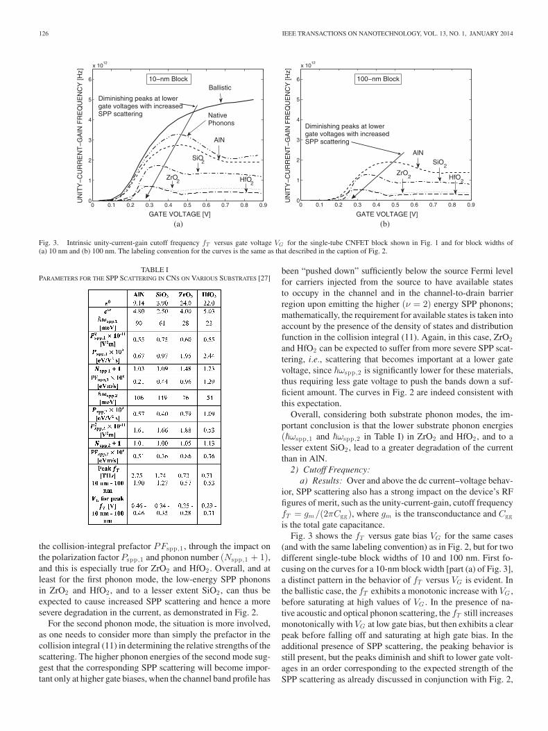
Fig. 3. Intrinsic unity-current-gain cutoff frequency fT versus gate voltage VG for the single-tube CNFET block shown in Fig. 1 and for block widths of(a) 10 nm and (b) 100 nm. The labeling convention for the curves is the same as that described in the caption of Fig. 2.
TABLE IPARAMETERS FOR THE SPP SCATTERING IN CNS ON VARIOUS SUBSTRATES [27]
the collision-integral prefactor PFspp,1 , through the impact onthe polarization factor Pspp,1 and phonon number (Nspp,1 + 1),and this is especially true for ZrO2 and HfO2 . Overall, and atleast for the first phonon mode, the low-energy SPP phononsin ZrO2 and HfO2 , and to a lesser extent SiO2 , can thus beexpected to cause increased SPP scattering and hence a moresevere degradation in the current, as demonstrated in Fig. 2.
For the second phonon mode, the situation is more involved,as one needs to consider more than simply the prefactor in thecollision integral (11) in determining the relative strengths of thescattering. The higher phonon energies of the second mode sug-gest that the corresponding SPP scattering will become impor-tant only at higher gate biases, when the channel band profile has
been “pushed down” sufficiently below the source Fermi levelfor carriers injected from the source to have available statesto occupy in the channel and in the channel-to-drain barrierregion upon emitting the higher (ν = 2) energy SPP phonons;mathematically, the requirement for available states is taken intoaccount by the presence of the density of states and distributionfunction in the collision integral (11). Again, in this case, ZrO2and HfO2 can be expected to suffer from more severe SPP scat-tering, i.e., scattering that becomes important at a lower gatevoltage, since �ωspp,2 is significantly lower for these materials,thus requiring less gate voltage to push the bands down a suf-ficient amount. The curves in Fig. 2 are indeed consistent withthis expectation.
Overall, considering both substrate phonon modes, the im-portant conclusion is that the lower substrate phonon energies(�ωspp,1 and �ωspp,2 in Table I) in ZrO2 and HfO2 , and to alesser extent SiO2 , lead to a greater degradation of the currentthan in AlN.
2) Cutoff Frequency:a) Results: Over and above the dc current–voltage behav-
ior, SPP scattering also has a strong impact on the device’s RFfigures of merit, such as the unity-current-gain, cutoff frequencyfT = gm /(2πCgg), where gm is the transconductance and Cggis the total gate capacitance.
Fig. 3 shows the fT versus gate bias VG for the same cases(and with the same labeling convention) as in Fig. 2, but for twodifferent single-tube block widths of 10 and 100 nm. First fo-cusing on the curves for a 10-nm block width [part (a) of Fig. 3],a distinct pattern in the behavior of fT versus VG is evident. Inthe ballistic case, the fT exhibits a monotonic increase with VG ,before saturating at high values of VG . In the presence of na-tive acoustic and optical phonon scattering, the fT still increasesmonotonically with VG at low gate bias, but then exhibits a clearpeak before falling off and saturating at high gate bias. In theadditional presence of SPP scattering, the peaking behavior isstill present, but the peaks diminish and shift to lower gate volt-ages in an order corresponding to the expected strength of theSPP scattering as already discussed in conjunction with Fig. 2,
AHMED et al.: IMPACT OF THE SUBSTRATE MATERIAL ON THE RF PERFORMANCE OF CARBON-NANOTUBE TRANSISTORS 127
(a) (b)
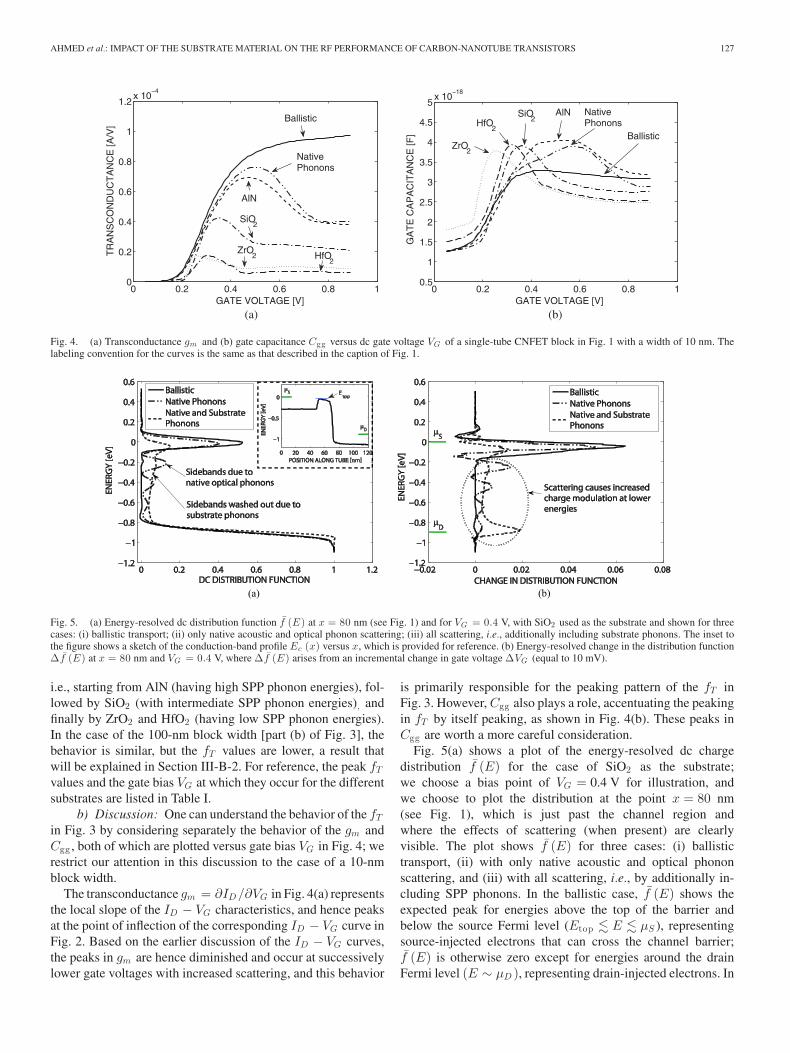
Fig. 4. (a) Transconductance gm and (b) gate capacitance Cgg versus dc gate voltage VG of a single-tube CNFET block in Fig. 1 with a width of 10 nm. Thelabeling convention for the curves is the same as that described in the caption of Fig. 1.
(a) (b)
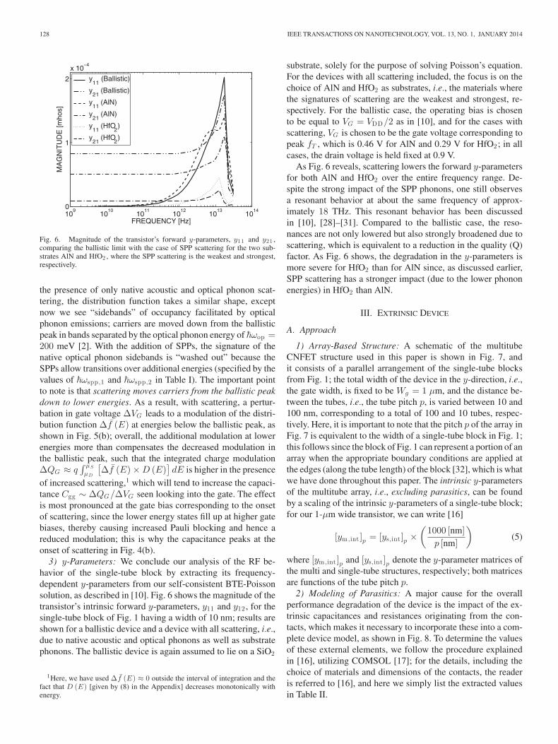
Fig. 5. (a) Energy-resolved dc distribution function f (E) at x = 80 nm (see Fig. 1) and for VG = 0.4 V, with SiO2 used as the substrate and shown for threecases: (i) ballistic transport; (ii) only native acoustic and optical phonon scattering; (iii) all scattering, i.e., additionally including substrate phonons. The inset tothe figure shows a sketch of the conduction-band profile Ec (x) versus x, which is provided for reference. (b) Energy-resolved change in the distribution functionΔf (E) at x = 80 nm and VG = 0.4 V, where Δf (E) arises from an incremental change in gate voltage ΔVG (equal to 10 mV).
i.e., starting from AlN (having high SPP phonon energies), fol-lowed by SiO2 (with intermediate SPP phonon energies), andfinally by ZrO2 and HfO2 (having low SPP phonon energies).In the case of the 100-nm block width [part (b) of Fig. 3], thebehavior is similar, but the fT values are lower, a result thatwill be explained in Section III-B-2. For reference, the peak fT
values and the gate bias VG at which they occur for the differentsubstrates are listed in Table I.
b) Discussion: One can understand the behavior of the fT
in Fig. 3 by considering separately the behavior of the gm andCgg , both of which are plotted versus gate bias VG in Fig. 4; werestrict our attention in this discussion to the case of a 10-nmblock width.
The transconductance gm = ∂ID /∂VG in Fig. 4(a) representsthe local slope of the ID − VG characteristics, and hence peaksat the point of inflection of the corresponding ID − VG curve inFig. 2. Based on the earlier discussion of the ID − VG curves,the peaks in gm are hence diminished and occur at successivelylower gate voltages with increased scattering, and this behavior
is primarily responsible for the peaking pattern of the fT inFig. 3. However, Cgg also plays a role, accentuating the peakingin fT by itself peaking, as shown in Fig. 4(b). These peaks inCgg are worth a more careful consideration.
Fig. 5(a) shows a plot of the energy-resolved dc chargedistribution f (E) for the case of SiO2 as the substrate;we choose a bias point of VG = 0.4 V for illustration, andwe choose to plot the distribution at the point x = 80 nm(see Fig. 1), which is just past the channel region andwhere the effects of scattering (when present) are clearlyvisible. The plot shows f (E) for three cases: (i) ballistictransport, (ii) with only native acoustic and optical phononscattering, and (iii) with all scattering, i.e., by additionally in-cluding SPP phonons. In the ballistic case, f (E) shows theexpected peak for energies above the top of the barrier andbelow the source Fermi level (Etop � E � μS ), representingsource-injected electrons that can cross the channel barrier;f (E) is otherwise zero except for energies around the drainFermi level (E ∼ μD ), representing drain-injected electrons. In
128 IEEE TRANSACTIONS ON NANOTECHNOLOGY, VOL. 13, NO. 1, JANUARY 2014
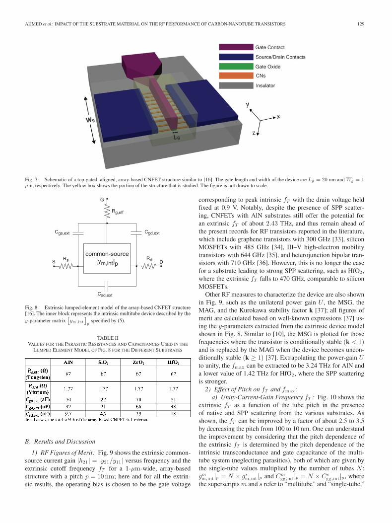
Fig. 6. Magnitude of the transistor’s forward y-parameters, y11 and y21 ,comparing the ballistic limit with the case of SPP scattering for the two sub-strates AlN and HfO2 , where the SPP scattering is the weakest and strongest,respectively.
the presence of only native acoustic and optical phonon scat-tering, the distribution function takes a similar shape, exceptnow we see “sidebands” of occupancy facilitated by opticalphonon emissions; carriers are moved down from the ballisticpeak in bands separated by the optical phonon energy of �ωop =200 meV [2]. With the addition of SPPs, the signature of thenative optical phonon sidebands is “washed out” because theSPPs allow transitions over additional energies (specified by thevalues of �ωspp,1 and �ωspp,2 in Table I). The important pointto note is that scattering moves carriers from the ballistic peakdown to lower energies. As a result, with scattering, a pertur-bation in gate voltage ΔVG leads to a modulation of the distri-bution function Δf (E) at energies below the ballistic peak, asshown in Fig. 5(b); overall, the additional modulation at lowerenergies more than compensates the decreased modulation inthe ballistic peak, such that the integrated charge modulationΔQG ≈ q
∫ μS
μD
[
Δf (E) × D (E)]
dE is higher in the presence
of increased scattering,1 which will tend to increase the capaci-tance Cgg ∼ ΔQG/ΔVG seen looking into the gate. The effectis most pronounced at the gate bias corresponding to the onsetof scattering, since the lower energy states fill up at higher gatebiases, thereby causing increased Pauli blocking and hence areduced modulation; this is why the capacitance peaks at theonset of scattering in Fig. 4(b).
3) y-Parameters: We conclude our analysis of the RF be-havior of the single-tube block by extracting its frequency-dependent y-parameters from our self-consistent BTE-Poissonsolution, as described in [10]. Fig. 6 shows the magnitude of thetransistor’s intrinsic forward y-parameters, y11 and y12 , for thesingle-tube block of Fig. 1 having a width of 10 nm; results areshown for a ballistic device and a device with all scattering, i.e.,due to native acoustic and optical phonons as well as substratephonons. The ballistic device is again assumed to lie on a SiO2
1Here, we have used Δf (E) ≈ 0 outside the interval of integration and thefact that D (E) [given by (8) in the Appendix] decreases monotonically withenergy.
substrate, solely for the purpose of solving Poisson’s equation.For the devices with all scattering included, the focus is on thechoice of AlN and HfO2 as substrates, i.e., the materials wherethe signatures of scattering are the weakest and strongest, re-spectively. For the ballistic case, the operating bias is chosento be equal to VG = VDD/2 as in [10], and for the cases withscattering, VG is chosen to be the gate voltage corresponding topeak fT , which is 0.46 V for AlN and 0.29 V for HfO2 ; in allcases, the drain voltage is held fixed at 0.9 V.
As Fig. 6 reveals, scattering lowers the forward y-parametersfor both AlN and HfO2 over the entire frequency range. De-spite the strong impact of the SPP phonons, one still observesa resonant behavior at about the same frequency of approx-imately 18 THz. This resonant behavior has been discussedin [10], [28]–[31]. Compared to the ballistic case, the reso-nances are not only lowered but also strongly broadened due toscattering, which is equivalent to a reduction in the quality (Q)factor. As Fig. 6 shows, the degradation in the y-parameters ismore severe for HfO2 than for AlN since, as discussed earlier,SPP scattering has a stronger impact (due to the lower phononenergies) in HfO2 than AlN.
III. EXTRINSIC DEVICE
A. Approach
1) Array-Based Structure: A schematic of the multitubeCNFET structure used in this paper is shown in Fig. 7, andit consists of a parallel arrangement of the single-tube blocksfrom Fig. 1; the total width of the device in the y-direction, i.e.,the gate width, is fixed to be Wg = 1 μm, and the distance be-tween the tubes, i.e., the tube pitch p, is varied between 10 and100 nm, corresponding to a total of 100 and 10 tubes, respec-tively. Here, it is important to note that the pitch p of the array inFig. 7 is equivalent to the width of a single-tube block in Fig. 1;this follows since the block of Fig. 1 can represent a portion of anarray when the appropriate boundary conditions are applied atthe edges (along the tube length) of the block [32], which is whatwe have done throughout this paper. The intrinsic y-parametersof the multitube array, i.e., excluding parasitics, can be foundby a scaling of the intrinsic y-parameters of a single-tube block;for our 1-μm wide transistor, we can write [16]
[ym ,int ]p = [ys,int ]p ×(
1000 [nm]p [nm]
)
(5)
where [ym ,int ]p and [ys,int ]p denote the y-parameter matrices ofthe multi and single-tube structures, respectively; both matricesare functions of the tube pitch p.
2) Modeling of Parasitics: A major cause for the overallperformance degradation of the device is the impact of the ex-trinsic capacitances and resistances originating from the con-tacts, which makes it necessary to incorporate these into a com-plete device model, as shown in Fig. 8. To determine the valuesof these external elements, we follow the procedure explainedin [16], utilizing COMSOL [17]; for the details, including thechoice of materials and dimensions of the contacts, the readeris referred to [16], and here we simply list the extracted valuesin Table II.
AHMED et al.: IMPACT OF THE SUBSTRATE MATERIAL ON THE RF PERFORMANCE OF CARBON-NANOTUBE TRANSISTORS 129
Fig. 7. Schematic of a top-gated, aligned, array-based CNFET structure similar to [16]. The gate length and width of the device are Lg = 20 nm and Wg = 1μm, respectively. The yellow box shows the portion of the structure that is studied. The figure is not drawn to scale.
Fig. 8. Extrinsic lumped-element model of the array-based CNFET structure[16]. The inner block represents the intrinsic multitube device described by they-parameter matrix
[
ym , int]
pspecified by (5).
TABLE IIVALUES FOR THE PARASITIC RESISTANCES AND CAPACITANCES USED IN THE
LUMPED ELEMENT MODEL OF FIG. 8 FOR THE DIFFERENT SUBSTRATES
B. Results and Discussion
1) RF Figures of Merit: Fig. 9 shows the extrinsic common-source current gain |h21 | = |y21/y11 | versus frequency and theextrinsic cutoff frequency fT for a 1-μm-wide, array-basedstructure with a pitch p = 10nm; here and for all the extrin-sic results, the operating bias is chosen to be the gate voltage
corresponding to peak intrinsic fT with the drain voltage heldfixed at 0.9 V. Notably, despite the presence of SPP scatter-ing, CNFETs with AlN substrates still offer the potential foran extrinsic fT of about 2.43 THz, and thus remain ahead ofthe present records for RF transistors reported in the literature,which include graphene transistors with 300 GHz [33], siliconMOSFETs with 485 GHz [34], III–V high-electron mobilitytransistors with 644 GHz [35], and heterojunction bipolar tran-sistors with 710 GHz [36]. However, this is no longer the casefor a substrate leading to strong SPP scattering, such as HfO2 ,where the extrinsic fT falls to 470 GHz, comparable to siliconMOSFETs.
Other RF measures to characterize the device are also shownin Fig. 9, such as the unilateral power gain U , the MSG, theMAG, and the Kurokawa stability factor k [37]; all figures ofmerit are calculated based on well-known expressions [37] us-ing the y-parameters extracted from the extrinsic device modelshown in Fig. 8. Similar to [10], the MSG is plotted for thosefrequencies where the transistor is conditionally stable (k < 1)and is replaced by the MAG when the device becomes uncon-ditionally stable (k ≥ 1) [37]. Extrapolating the power-gain Uto unity, the fmax can be extracted to be 3.24 THz for AlN anda lower value of 1.42 THz for HfO2 , where the SPP scatteringis stronger.
2) Effect of Pitch on fT and fmax :a) Unity-Current-Gain Frequency fT : Fig. 10 shows the
extrinsic fT as a function of the tube pitch in the presenceof native and SPP scattering from the various substrates. Asshown, the fT can be improved by a factor of about 2.5 to 3.5by decreasing the pitch from 100 to 10 nm. One can understandthe improvement by considering that the pitch dependence ofthe extrinsic fT is determined by the pitch dependence of theintrinsic transconductance and gate capacitance of the multi-tube system (neglecting parasitics), both of which are given bythe single-tube values multiplied by the number of tubes N :gm
m ,int |p = N × gsm ,int |p and Cm
gg ,int |p = N × Csgg ,int |p , where
the superscripts m and s refer to “multitube” and “single-tube,”
130 IEEE TRANSACTIONS ON NANOTECHNOLOGY, VOL. 13, NO. 1, JANUARY 2014
Fig. 9. Magnitude of the common-source current gain |h21 |, unilateral power gain U , MSG, MAG, and the stability factor k as function of frequency for theCNFET of Fig. 7 with a tube pitch p = 10 nm and with (a) AlN and (b) HfO2 as substrates. The extrapolated fT and fm ax are also shown.
Fig. 10. Extrapolated extrinsic fT of the array-based CNFET structure as afunction of tube pitch in the presence of native and SPP scattering for differentsubstrates.
respectively, and where the notation “|p” is used to emphasizethat the corresponding quantities depend on the tube pitch p.To first order, we can estimate the pitch dependence by writ-ing the extrinsic fT ∼ gm
m ,int |p/Cmgg ,int |p = gs
m ,int |p/Csgg ,int |p .
With a decrease in pitch (higher tube density), both gsm ,int |p
and Csgg ,int |p decrease due to tube screening [32]; the impor-
tant point is that Csgg ,int |p decreases by 30–35% (depending on
the substrate) whereas gsm ,int |p reduces by only 3–7% when the
pitch is scaled down from 100 to 10 nm (not shown). This dif-ference in reduction results in an effective increase of the fT
as reported in [32] and as depicted in Fig. 10; it also explainswhy the fT results for the 10-nm block presented earlier inFig. 3(a) exceed those for the 100-nm block in Fig. 3(b). Moreimportantly, Fig. 10 shows that the RF performance advantageof an AlN substrate continues to exist for the extrinsic cutoff fre-quency fT , a consequence of AlN’s high-energy SPP phononscausing weaker SPP scattering as compared to HfO2 and ZrO2substrates, as discussed earlier in Section II.
b) Unity-Power-Gain Frequency fmax : Contrary to thefT , the transistor’s fmax is much less susceptible to variationsof the tube pitch; for example, it grows by a factor of about 1.2
Fig. 11. fm ax of the array-based CNFET structure as function of tube pitchin the presence of native and SPP scattering for different substrates.
to 1.5 for the HfO2 and ZrO2 substrates and not at all for SiO2and AlN when the pitch is decreased from 100 to 10 nm, as canbe discerned from Fig. 11. This behavior of the fmax can beexplained with the aid of the approximate expression [38], [39]
fmax ≈√
fT
8πRg ,eff Cgd,eff(6)
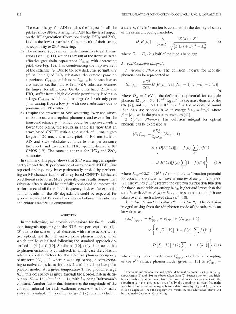
which has been shown to reproduce the pitch-dependence of thenumerically obtained fmax quite well [16]. Here, Rg ,eff is theeffective gate resistance (shown in Fig. 8) and Cgd,eff is the totaleffective gate-drain capacitance, which can be expressed as [16]
Cgd,eff = N × Csgd,int |p + Cgd,ext (7)
where Csgd,int |p refers to the gate-drain capacitance of the in-
trinsic single-tube CNFET block of Fig. 1, and Cgd,ext is the ex-ternal gate-drain capacitance of the array-based CNFET shownin Fig. 6 and listed in Table II. Decreasing the pitch correspondsto a larger N , causing the term N × Cs
gd,int |p and thus Cgd,effto grow, as Fig. 12 shows; this increase of Cgd,eff compensatesthe increase of the fT discussed in conjunction with Fig. 10,causing the fmax to remain almost unaffected from a variationof the pitch [16].
AHMED et al.: IMPACT OF THE SUBSTRATE MATERIAL ON THE RF PERFORMANCE OF CARBON-NANOTUBE TRANSISTORS 131
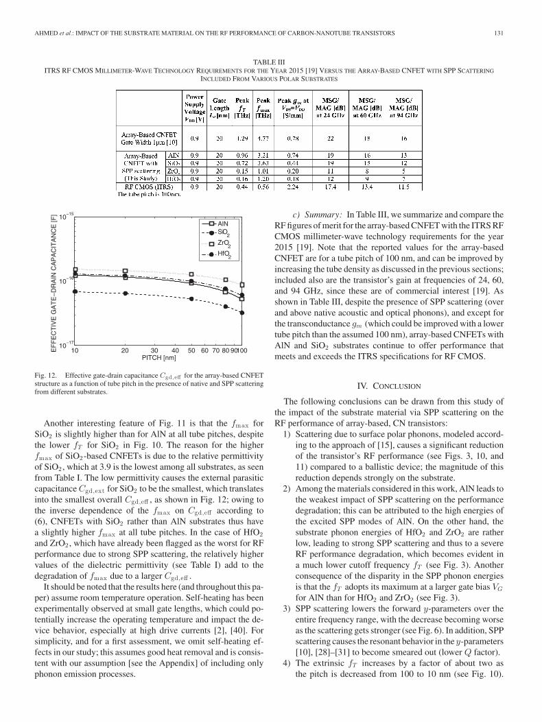
TABLE IIIITRS RF CMOS MILLIMETER-WAVE TECHNOLOGY REQUIREMENTS FOR THE YEAR 2015 [19] VERSUS THE ARRAY-BASED CNFET WITH SPP SCATTERING
INCLUDED FROM VARIOUS POLAR SUBSTRATES
Fig. 12. Effective gate-drain capacitance Cgd ,eff for the array-based CNFETstructure as a function of tube pitch in the presence of native and SPP scatteringfrom different substrates.
Another interesting feature of Fig. 11 is that the fmax forSiO2 is slightly higher than for AlN at all tube pitches, despitethe lower fT for SiO2 in Fig. 10. The reason for the higherfmax of SiO2-based CNFETs is due to the relative permittivityof SiO2 , which at 3.9 is the lowest among all substrates, as seenfrom Table I. The low permittivity causes the external parasiticcapacitance Cgd,ext for SiO2 to be the smallest, which translatesinto the smallest overall Cgd,eff , as shown in Fig. 12; owing tothe inverse dependence of the fmax on Cgd,eff according to(6), CNFETs with SiO2 rather than AlN substrates thus havea slightly higher fmax at all tube pitches. In the case of HfO2and ZrO2 , which have already been flagged as the worst for RFperformance due to strong SPP scattering, the relatively highervalues of the dielectric permittivity (see Table I) add to thedegradation of fmax due to a larger Cgd,eff .
It should be noted that the results here (and throughout this pa-per) assume room temperature operation. Self-heating has beenexperimentally observed at small gate lengths, which could po-tentially increase the operating temperature and impact the de-vice behavior, especially at high drive currents [2], [40]. Forsimplicity, and for a first assessment, we omit self-heating ef-fects in our study; this assumes good heat removal and is consis-tent with our assumption [see the Appendix] of including onlyphonon emission processes.
c) Summary: In Table III, we summarize and compare theRF figures of merit for the array-based CNFET with the ITRS RFCMOS millimeter-wave technology requirements for the year2015 [19]. Note that the reported values for the array-basedCNFET are for a tube pitch of 100 nm, and can be improved byincreasing the tube density as discussed in the previous sections;included also are the transistor’s gain at frequencies of 24, 60,and 94 GHz, since these are of commercial interest [19]. Asshown in Table III, despite the presence of SPP scattering (overand above native acoustic and optical phonons), and except forthe transconductance gm (which could be improved with a lowertube pitch than the assumed 100 nm), array-based CNFETs withAlN and SiO2 substrates continue to offer performance thatmeets and exceeds the ITRS specifications for RF CMOS.
IV. CONCLUSION
The following conclusions can be drawn from this study ofthe impact of the substrate material via SPP scattering on theRF performance of array-based, CN transistors:
1) Scattering due to surface polar phonons, modeled accord-ing to the approach of [15], causes a significant reductionof the transistor’s RF performance (see Figs. 3, 10, and11) compared to a ballistic device; the magnitude of thisreduction depends strongly on the substrate.
2) Among the materials considered in this work, AlN leads tothe weakest impact of SPP scattering on the performancedegradation; this can be attributed to the high energies ofthe excited SPP modes of AlN. On the other hand, thesubstrate phonon energies of HfO2 and ZrO2 are ratherlow, leading to strong SPP scattering and thus to a severeRF performance degradation, which becomes evident ina much lower cutoff frequency fT (see Fig. 3). Anotherconsequence of the disparity in the SPP phonon energiesis that the fT adopts its maximum at a larger gate bias VG
for AlN than for HfO2 and ZrO2 (see Fig. 3).3) SPP scattering lowers the forward y-parameters over the
entire frequency range, with the decrease becoming worseas the scattering gets stronger (see Fig. 6). In addition, SPPscattering causes the resonant behavior in the y-parameters[10], [28]–[31] to become smeared out (lower Q factor).
4) The extrinsic fT increases by a factor of about two asthe pitch is decreased from 100 to 10 nm (see Fig. 10).
132 IEEE TRANSACTIONS ON NANOTECHNOLOGY, VOL. 13, NO. 1, JANUARY 2014
The extrinsic fT for AlN remains the largest for all thepitches since SPP scattering with AlN has the least impacton the RF degradation. Correspondingly, HfO2 and ZrO2lead to the lowest extrinsic fT as a result of their strongsusceptibility to SPP scattering.
5) The extrinsic fmax remains quite insensitive to pitch vari-ations (see Fig. 11), which is a result of the increase in theeffective gate-drain capacitance Cgd,eff with decreasingpitch (see Fig. 12), thus counteracting the improvementof the extrinsic fT . Due to the low dielectric permittivity(ε0 in Table I) of SiO2 substrates, the external parasiticcapacitance Cgd,ext and thus the Cgd,eff is the smallest; asa consequence, the fmax with an SiO2 substrate becomesthe largest for all pitches. On the other hand, ZrO2 andHfO2 suffer from a high dielectric permittivity leading toa large Cgd,ext , which tends to degrade the already poorfmax arising from a low fT with these substrates due topronounced SPP scattering.
6) Despite the presence of SPP scattering (over and abovenative acoustic and optical phonons), and except for thetransconductance gm (which could be improved with alower tube pitch), the results in Table III show that anarray-based CNFET with a gate width of 1 μm, a gatelength of 20 nm, and a tube pitch of 100 nm built onAlN and SiO2 substrates continue to offer performancethat meets and exceeds the ITRS specifications for RFCMOS [19]. The same is not true for HfO2 and ZrO2substrates.
In summary, this paper shows that SPP scattering can signifi-cantly impact the RF performance of array-based CNFETs. Ourreported findings may be experimentally probed by perform-ing an RF characterization of array-based CNFETs fabricatedon different substrates. More generally, our results suggest thatsubstrate effects should be carefully considered to improve theperformance of all future high-frequency devices; for example,similar results on the RF degradation could be expected forgraphene-based FETs, since the distance between the substrateand channel material is comparable.
APPENDIX
In the following, we provide expressions for the full colli-sion integrals appearing in the BTE transport equations (1)–(3) due to the scattering of electrons with native acoustic, na-tive optical, and the νth surface polar phonon modes, all ofwhich can be calculated following the standard approach de-scribed in [41] and [10]. Similar to [10], only the process dueto phonon emission is considered, in which case the collisionintegrals contain factors for the effective phonon occupancyof the form (Nγ + 1), where γ = ac, op, or spp, ν, correspond-ing to native acoustic, native optical, and the νth surface polarphonon modes. At a given temperature T and phonon energy�ωγ , this occupancy is given through the Bose–Einstein distri-bution, Nγ = 1/
(
e�ωγ /kB T − 1)
, with kB being Boltzmann’sconstant. Another factor that determines the magnitude of thecollision integral for each scattering process γ is how manystates are available at a specific energy E (k) for an electron in
a state k; this information is contained in the density of statesof the semiconducting nanotube,
D [E (k)] =8
3πa0tE
[E (k) + E0 ]√
[E (k) + E0 ]2 − E2
0
(8)
where E0 = Eg/2 is half of the tube’s band gap.
A. Full Collision Integrals
1) Acoustic Phonons: The collision integral for acousticphonons can be represented as
(Sof)ac =πD2
A
2ρvsD [E (k)] |2k| (Nac + 1) [f (−k) − f (k)]
(9)where DA = 5 eV is the deformation potential for acousticphonons [2], ρ = 3 × 10⁻¹⁵ kg m−1 is the mass density of theCN [9], and vs = 21.1 × 10³ m s−1 is the velocity of sound[8].2 Acoustic phonons have an energy �ωac = �vsβ, whereβ = |k − k′| is the phonon momentum [41].
2) Optical Phonons: The collision integral for opticalphonons can be expressed as
(Sof)op =πD2
op
2ρωop(Nop + 1)
×{
D[E+(k)][1 − f(k)]∑
k+
f(k+)
− D[E−(k)]f(k)∑
k−
[1 − f(k−)]
}
(10)
where Dop=12.8 × 10¹⁰ eV m−1 is the deformation potentialfor optical phonons, which have an energy of �ωop = 200 meV[2]. The values f (k±) refer to the electron distribution functionfor those states with an energy �ωop higher and lower than thestate k, with E± = E (k) ± �ωop . The summations in (10) aretaken over all such allowed states k± [10].
3) Substrate Surface Polar Phonons (SPP): The collisionintegral arising from the νth phonon mode of the substrate canbe written as
(Sof)spp,ν = F 2spp,ν × Pspp,ν × (Nspp,ν + 1)
×{
D[
E+ (k)]
[1 − f (k)]∑
k+
f(
k+)
− D[
E− (k)]
f (k)∑
k−
[
1 − f(
k−)]
}
(11)
where the symbols are as follows: F 2spp,ν is the Frohlich coupling
of the νth surface phonon mode, given in [15] as F 2spp,ν =
2The values of the acoustic and optical deformation potentials DA and Dopappearing in (9) and (10) have been taken from [2], because the low- and high-bias mean-free paths computed from them were shown to be consistent with theexperiments in the same paper; specifically, the experimental mean-free pathswere found to lie within the upper bounds determined by DA and Dop , whichis to be expected since the experiments would include additional (above andbeyond native) sources of scattering.
AHMED et al.: IMPACT OF THE SUBSTRATE MATERIAL ON THE RF PERFORMANCE OF CARBON-NANOTUBE TRANSISTORS 133
�ω s p p , ν
2πε0
(
1ε∞+1 − 1
ε0 +1
)
, where ε0 and ε∞ are the low- and
high-frequency dielectric constants of the polar substrate, andε0 is the vacuum permittivity; d is the tube diameter; Pspp,ν
is indicative of the strength of the polarization field due to thesubstrate phonons at a distance s away from the substrate, givenby
Pspp,ν =4π2q2e−2sqz
�dqz
√
2π (d + 2s) qz
(12)
where s is the separation of the surface of the tube from thesubstrate and is set to 0.35 nm, as given by the van der Waalsinteraction [15], and �qz is the electron momentum transferalong the tube axis, determined from [11], [15]
�vF qz = {�ωspp,ν (2Δ + �ωspp,ν )}1/2 (13)
with vF ≈ 108 cm s−1 being the Fermi velocity and 2Δ ≈0.9/d eV. The values for the phonon energies and the dielectricconstants of the polar substrates are taken from [27] and arelisted in Table I.
B. Linearized Collision Integrals
The small-signal form of the collision integrals can be ob-tained in a manner similar to the linearization of the BTE out-lined in Section II-A by inserting the ansatz f = f + f ejωt intothe full expressions (9)–(11) for the collision integrals and re-taining terms to linear order in f . For each type of scattering,the results are as follows:
So
{
f , f}
ac=
πD2A
2ρvsD [E (k)] |2k| (Nac + 1)
[
f (−k)−f (k)]
(14)
So
{
f , f}
op=
πD2op
2ρωop(Nop + 1)
×{
D[
E+ (k)]∑
k+
[
1 − f (k)]
f(
k+)
− f(
k+)
f (k)
− D[
E− (k)]∑
k−
[
1−f(
k−)]
f (k)−f (k) f(
k−)
}
(15)
and
So
{
f , f}
spp,ν= F 2
spp,ν × Pspp,ν × (Nspp,ν + 1)
×{
D[
E+ (k)]∑
k+
[
1 − f (k)]
f(
k+)
− f(
k+)
f (k)
− D[
E− (k)]∑
k−
[
1 − f(
k−)]
f (k) − f (k) f(
k−)
}
.
(16)
REFERENCES
[1] C. Rutherglen, D. Jain, and P. Burke, “Nanotube electronics for radiofre-quency applications,” Nat. Nano, vol. 4, no. 12, pp. 811–819, 2009.
[2] J. Y. Park, S. Rosenblatt, Y. Yaish, V. Sazonova, H. Ustunel, S. Braig,T. A. Arias, P. W. Brouwer, and P. L. McEuen, “Electron-phonon scatter-ing in metallic single-walled carbon nanotubes,” Nano Lett., vol. 4, no. 3,pp. 517–520, 2004.
[3] T. Durkop, S. A. Getty, E. Cobas, and M. S. Fuhrer, “Extraordinary mo-bility in semiconducting carbon nanotubes,” Nano Lett., vol. 4, no. 1,pp. 35–39, 2004.
[4] X. Zhou, J. Y. Park, S. Huang, J. Liu, and P. L. McEuen, “Band structure,phonon scattering, and the performance limit of single-walled carbonnanotube transistors,” Phys. Rev. Lett., vol. 95, no. 14, pp. 146805-1–146805-4, 2005.
[5] V. Perebeinos, J. Tersoff, and P. Avouris, “Electron-phonon interaction andtransport in semiconducting carbon nanotubes,” Phys. Rev. Lett., vol. 94,no. 8, pp. 086802-1–086802-4, 2005.
[6] J. Guo and M. Lundstrom, “Role of phonon scattering in carbon nanotubefield-effect transistors,” Appl. Phys. Lett., vol. 86, no. 19, pp. 193103-1–193103-3, 2005.
[7] A. Svizhenko and M. P. Anantram, “Effect of scattering and contacts oncurrent and electrostatics in carbon nanotubes,” Phys. Rev. B, vol. 72,no. 8, pp. 085430-1–085430-10, 2005.
[8] S. O. Koswatta, S. Hasan, M. S. Lundstrom, M. P. Anantram, andD. E. Nikonov, “Ballisticity of nanotube field-effect transistors: Role ofphonon energy and gate bias,” Appl. Phys. Lett., vol. 89, no. 2, pp. 23125-1–23125-3, 2006.
[9] G. Pennington, N. Goldsman, A. Akturk, and A. E. Wickenden, “Defor-mation potential carrier-phonon scattering in semiconducting carbon nan-otube transistors,” Appl. Phys. Lett., vol. 90, no. 6, pp. 62110-1–62110-3,2007.
[10] N. Paydavosi, A. U. Alam, S. Ahmed, K. D. Holland, J. P. Rebstock,and M. Vaidyanathan, “RF performance potential of array-based carbon-nanotube transistors—Part I: Intrinsic results,” IEEE Trans. Electron De-vices, vol. 58, no. 7, pp. 1928–1940, Jul. 2011.
[11] A. G. Petrov and S. V. Rotkin, “Energy relaxation of hot carriers in single-wall carbon nanotubes by surface optical phonons of the substrate,” JETPLett., vol. 84, no. 3, pp. 156–160, 2006.
[12] V. Perebeinos, J. Tersoff, and P. Avouris, “Mobility in semiconducting car-bon nanotubes at finite carrier density,” Nano Lett., vol. 6, no. 2, pp. 205–208, 2006.
[13] B. Chandra, V. Perebeinos, S. Berciaud, J. Katoch, M. Ishigami, P. Kim,T. F. Heinz, and J. Hone, “Low bias electron scattering in structure-identified single wall carbon nanotubes: Role of substrate polar phonons,”Phys. Rev. Lett., vol. 107, no. 14, pp. 146601-1–146601-4, 2011.
[14] G. D. Mahan, “Surface polaritons and the theory of image charges,” Phys.Rev. B, vol. 5, no. 2, pp. 739–744, 1972.
[15] V. Perebeinos, S. V. Rotkin, A. G. Petrov, and P. Avouris, “The effectsof substrate phonon mode scattering on transport in carbon nanotubes,”Nano Lett., vol. 9, no. 1, pp. 312–316, 2009.
[16] N. Paydavosi, J. P. Rebstock, K. D. Holland, S. Ahmed, A. U. Alam,and M. Vaidyanathan, “RF performance potential of array-based carbon-nanotube transistors—Part II: Extrinsic results,” IEEE Trans. ElectronDevices, vol. 58, no. 7, pp. 1941–1951, Jul. 2011.
[17] COMSOL Multiphysics Version 3.5 a. COMSOL, Inc., Stockholm,Sweden, 2008
[18] R. Ludwig and G. Bogdanov, RF Circuit Design: Theory and Applications.2nd ed. Upper Saddle River, NJ, USA: Prentice-Hall, 2009.
[19] “Radio frequency and analog/mixed-signal technologies for wirelesscommunications,” International Technology Roadmap for Semicon-ductors, 2009 Edition. [Online]. Available: http://www.itrs.net/Links/2009ITRS/2009Chapters_2009Tables/2009_Wireless.pdf
[20] S. Datta, Quantum Transport: Atom to Transistor. Cambridge, U. K.:Cambridge University Press, 2005.
[21] S. Fratini and F. Guinea, “Substrate-limited electron dynamics ingraphene,” Phys. Rev. B, vol. 77, no. 19, pp. 195415-1–195415-6, 2008.
[22] A. Konar, T. Fang, and D. Jena, “Effect of high-k gate dielectrics on chargetransport in graphene-based field effect transistors,” Phys. Rev. B, vol. 82,no. 11, pp. 115452-1–115452-7, 2010.
[23] Z. Y. Ong and M. V. Fischetti, “Theory of interfacial plasmon–phononscattering in supported graphene,” Phys. Rev. B, vol. 86, no. 16,pp. 165422-1–165422-15, 2012.
[24] Z. Y. Ong and M. V. Fischetti, “Erratum: Theory of interfacial plasmon–phonon scattering in supported graphene,” Phys. Rev. B, vol. 86, no. 19,pp. 199904-1–199904-2, 2012.
[25] Z. Y. Ong and M. V. Fischetti, “Top oxide thickness dependence of remotephonon and charged impurity scattering in top-gated graphene,” Appl.Phys. Lett., vol. 102, no. 18, pp. 183506–1–183506–4, 2013.
134 IEEE TRANSACTIONS ON NANOTECHNOLOGY, VOL. 13, NO. 1, JANUARY 2014
[26] F. Wang, D. J. Cho, B. Kessler, J. Deslippe, P. J. Schuck, S. G. Louie,A. Zettl, T. F. Heinz, and Y. R. Shen, “Observation of excitons in one-dimensional metallic single-walled carbon nanotubes,” Phys. Rev. Lett.,vol. 99, no. 22, pp. 227401-1–227401-4, 2007.
[27] M. V. Fischetti, D. A. Neumayer, and E. A. Cartier, “Effective electronmobility in Si inversion layers in metal-oxide-semiconductor systems witha high-k insulator: The role of remote phonon scattering,” J. Appl. Phys.,vol. 90, no. 9, pp. 4587–4608, 2001.
[28] N. Paydavosi, K. D. Holland, M. M. Zargham, and M. Vaidyanathan,“Understanding the frequency- and time-dependent behavior of ballis-tic carbon-nanotube transistors,” IEEE Trans. Nanotechnol., vol. 8, no. 2,pp. 234–244, Mar. 2009.
[29] N. Paydavosi, M. M. Zargham, K. D. Holland, C. M. Dublanko, andM. Vaidyanathan, “Non-quasi-static effects and the role of kinetic induc-tance in ballistic carbon-nanotube transistors,” IEEE Trans. Nanotechnol.,vol. 9, no. 4, pp. 449–463, 2010.
[30] D. Kienle, M. Vaidyanathan, and F. Leonard, “Self-consistent ac quantumtransport using nonequilibrium Green functions,” Phys. Rev. B, vol. 81,no. 11, pp. 115455-1–115455-10, 2010.
[31] D. Kienle and F. Leonard, “Terahertz response of carbon nanotube tran-sistors,” Phys. Rev. Lett., vol. 103, no. 2, pp. 026601-1–026601-4, 2009.
[32] K. Holland, N. Paydavosi, and M. Vaidyanathan, “Self-consistent simula-tion of array-based CNFETs: Impact of tube pitch on RF performance,”in Proc. 14th Int. Wireless Commun. Expo, Oct. 2010, pp. 291–294.
[33] L. Liao, Y. C. Lin, M. Bao, R. Cheng, J. Bai, Y. Liu, Y. Qu, K. L. Wang,Y. Huang, and X. Duan, “High-speed graphene transistors with a self-aligned nanowire gate,” Nature, vol. 467, pp. 305–308, 2010.
[34] S. Lee, B. Jagannathan, S. Narasimha, A. Chou, N. Zamdmer, J. Johnson,R. Williams, L. Wagner, J. Kim, J. Plouchart, J. Pekarik, S. Springer, andG. Freeman, “Record RF performance of 45-nm SOI CMOS technology,”in Proc. IEEE Int. Electron. Devices Meet., Dec. 2007, pp. 255–258.
[35] D. H. Kim and J. A. del Alamo, “30-nm InAs PHEMTs with fT =644 GHz and fm ax = 681 GHz,” IEEE Electron. Device Lett., vol. 31,no. 8, pp. 806–808, Aug. 2010.
[36] W. Hafez, W. Snodgrass, and M. Feng, “12.5 nm base pseudomorphicheterojunction bipolar transistors achieving fT = 710 GHz and fM AX= 340 GHz,” Appl. Phys. Lett., vol. 87, no. 25, pp. 252109-1–252109-3,2005.
[37] M. S. Gupta, “Power gain in feedback amplifiers, a classic revisited,” IEEETrans. Microw. Theory Tech., vol. 40, no. 5, pp. 864–879, May 1992.
[38] L. C. Castro and D. L. Pulfrey, “Extrapolated fm ax for carbon nanotubefield-effect transistors,” Nanotechnology, vol. 17, no. 1, pp. 300–304,2006.
[39] M. Vaidyanathan and D. L. Pulfrey, “Extrapolated fm ax of heterojunctionbipolar transistors,” IEEE Trans. Electron. Devices, vol. 46, no. 2, pp. 301–309, Feb. 1999.
[40] H. Dai, A. Javey, E. Pop, D. Mann, W. Kim, and Y. Lu, “Electrical transportproperties and field effect transistors of carbon nanotubes,” Nano, vol. 1,no. 1, pp. 1–13, 2006.
[41] M. Lundstrom, Fundamentals of Carrier Transport. 2nd ed. New York,NY, USA: Cambridge University Press, 2000.
Sabbir Ahmed received the B.Sc. and M.Sc. degreesin electrical and electronic engineering (EEE) fromthe Bangladesh University of Engineering and Tech-nology (BUET), Dhaka, Bangladesh, in 2005 and2007, respectively. In 2008, he joined the Univer-sity of Alberta, Edmonton, AB, Canada, where he iscurrently working towards the Ph.D. degree, on leavefrom BUET.
From 2005 to 2008, he was a Lecturer with theDepartment of EEE of BUET. His research inter-ests include the theory, modeling, and simulation of
nanoscale electronic devices, with an emphasis on the high-frequency andcircuit-level performance of III–V high-electron-mobility transistors, carbon-based transistors and solar cell devices.
Mr. Ahmed received the F. S. Chia Doctoral Scholarship in 2008 and 2009,and the Queen Elizabeth II Graduate Scholarship in 2010, 2011, and 2012 at theUniversity of Alberta.
Navid Paydavosi received the B.A.Sc. degree in elec-trical engineering from Shahid Beheshti University,Tehran, Iran, in 2005, and the Ph.D. degree in electri-cal engineering from the University of Alberta, Ed-monton, AB, Canada, in 2011.
He is currently a Postdoctoral Scholar with theBSIM Group in the University of California, Berke-ley, CA, USA. His research interests are in the the-ory and modeling of future alternatives to ordinarysilicon transistors, including carbon-based and III–V high-electron-mobility devices, with an emphasis
on the high-frequency characteristics relevant for RF applications, such as theextrinsic cutoff frequency, the attainable power gain, the unity-power-gain fre-quency, and linearity.
Dr. Paydavosi received the Queen Elizabeth II Graduate Scholarship forSeptember 2009 and January 2010, and two Tuition Supplement Awards inSeptember 2006 and April 2007 from the University of Alberta.
Ahsan Ul Alam received the B.Sc. and the M.Sc.degrees in electrical and electronic engineering fromthe Bangladesh University of Engineering and Tech-nology (BUET), Dhaka, Bangladesh, in 2005 and2007, respectively. Currently, he is on study leavefrom BUET, working toward the Ph.D. degree at theUniversity of Alberta, Edmonton, AB, Canada.
From 2005 to 2008, he was a Lecturer at BUET,teaching courses and performing research in the areaof semiconductor devices. His research interests inl-cude the theory and modeling of semiconductor de-
vices, where he has worked on topics ranging from the study of spin transport incarbon-based devices to the modeling of high-frequency distortion for wirelessapplications.
Mr. Alam received the Kintar-ul Huq Lashkar Gold Medal from BUET forsecuring the top position in his undergraduate studies. He also received the F. S.Chia Ph.D. Scholarship in the first two years and the Queen Elizabeth II Grad-uate Scholarship in the third, fourth, fifth, and sixth year of his Ph.D. studies atthe University of Alberta.
Kyle David Holland received the B.Sc. degree inengineering physics (nanoengineering option) fromthe University of Alberta, Edmonton, AB, Canada, in2009, where he is currently working toward the Ph.D.degree in electrical engineering.
His research interests include quantum simula-tion of carbon-based nanoelectronics, with an em-phasis on modeling the high-frequency performanceof graphene devices.
Mr. Holland currently holds an NSERC Alexan-der Graham Bell Canada Graduate Scholarship and
an Alberta Innovates Graduate Student Scholarship, and he was a recipient ofthe Ralph Steinhauer Award of Distinction.
AHMED et al.: IMPACT OF THE SUBSTRATE MATERIAL ON THE RF PERFORMANCE OF CARBON-NANOTUBE TRANSISTORS 135
Diego Kienle received the B.S. (Vordiplom) andthe M.S. (Diplom) degrees from the Universityof Bayreuth, Bayreuth, Germany, and the Ph.D.(Dr.rer.nat.) degree from the Research Center Julichand the University of Saarland, Saarbrucken, Ger-many, all in theoretical physics.
After Postdoctoral appointments with the Electri-cal and Computer Engineering Department at PurdueUniversity, West Lafayette, IN, USA, and the Mate-rial Science Department at Sandia National Labora-tories, CA, USA, he is currently with the Institute of
Theoretical Physics at the University of Bayreuth. His research interests includethe formal theory, modeling, and simulation of ac quantum electronic trans-port in nanoscale materials and devices with focus on the understanding of thequantum dynamic processes in low-dimensional materials and their potentialapplication in solid-state based terahertz devices. His past research interestswere in the theory and modeling of complex fluids by means of Brownian dy-namics with focus on many-body hydrodynamic interaction effects in dilutedpolymer solutions.
Mani Vaidyanathan (S’95–M’99) received the Ph.D. degree in electrical en-gineering from the University of British Columbia, Vancouver, BC, Canada, in1999.
He is currently an Associate Professor with the Department of Electrical andComputer Engineering at the University of Alberta, Edmonton, AB, Canada.His research interests include the modeling, simulation, and understanding ofelectronic devices for future technologies, with a present focus on the radio-frequency performance of carbon-nanotube and graphene-based devices.
Dr. Vaidyanathan is a recipient of the University of Alberta’s Provost’s Awardand the University of Alberta’s Alexander Rutherford Award, both for excel-lence in teaching.