1180 ieee transactions on nanotechnology,...
TRANSCRIPT
1180 IEEE TRANSACTIONS ON NANOTECHNOLOGY, VOL. 10, NO. 5, SEPTEMBER 2011
Comparative Study on Energy-Efficiencies ofSingle-Electron Transistor-Based Binary Full
Adders Including Nonideal EffectsJieun Lee, Jung Han Lee, Student Member, IEEE, In-Young Chung, Chang-Joon Kim,
Byung-Gook Park, Member, IEEE, Dong Myong Kim, Member, IEEE, and Dae Hwan Kim, Member, IEEE
Abstract—Performances and energy efficiencies of varioussingle-electron transistor-based (SET-based) binary full adders(FAs) are comparatively investigated with optimization of deviceparameters by means of simulation program with integrated circuitemphasis models including nonideal effects commonly observed inreally implemented SETs. The proposed binary decision diagram(BDD) cell-based 1-bit FA is the most promising in terms of energyefficiency (=0.3 aJ/state), power dissipation (P = 1.2 nW), delay(τ = 20 ps), and immunity to process variations (backgroundcharge noise ΔQ0 < ±0.112q and control gate capacitance mis-match ΔCcg < 0.5 × Ccg ) at the expense of hardware burden,compared with majority gate-based SET FAs (3.988 aJ/state, P =15.95 nW, τ = 52 ps, ΔQ0 < ±0.0392q, ΔCcg < 0.35 × Ccg ) andSET threshold logic gate-based FAs (3.845 aJ/state, P = 15.38 nW,τ = 107 ps, ΔQ0 < ±0.028q, ΔCcg < 0.2 × Ccg ). It is also foundthat the SET itself dominates the power dissipation in SET-basedFAs and the static dc power plays a significant role in power con-sumption in SET-based FAs, compared with the dynamic power,regardless of the FA type. In addition, SET-based BDD FAs arecompared with their CMOS counterparts.
Index Terms—Binary decision diagram (BDD), energy effi-ciency, full adders (FAs), nonideal effects, single-electron transistor(SET).
I. INTRODUCTION
B INARY full adder (FA) is a crucial block for overall arith-metic functions such as addition, subtraction, multiplica-
tion, division, and address calculation. An explosive demand
Manuscript received October 5, 2009; revised August 13, 2010 andFebruary 11, 2011; accepted February 22, 2011. Date of publication March 10,2011; date of current version September 8, 2011. This work was supported bythe Korea Science and Engineering Foundation (KOSEF) funded by the Koreagovernment (MEST) under Grant R01-2008-000-20835-0. The CAD softwarewas supported by IC Design Education Center (IDEC). The review of this paperwas arranged by Associate Editor K. Matsumoto.
J. Lee, D. M. Kim, and D. H. Kim are with the School of Electrical En-gineering, Kookmin University, Seongbuk-gu, Seoul, 136-702, Korea (e-mail:[email protected]; [email protected]; [email protected]).
J. H. Lee and B.-G. Park are with the School of Electrical Engineering andComputer Science, Seoul National University, Seoul, 151-742, Korea (e-mail:[email protected]; [email protected]).
I.-Y. Chung is with the Department of Electronics and Communications En-gineering, Kwangwoon University, Seoul 139-701, Korea (e-mail: [email protected]).
C.-J. Kim is with the Department of Chemical and Biological Engineeringand ERI, Gyeongsang National University, Gyeongnam 660-701, Korea (e-mail:[email protected]).
Color versions of one or more of the figures in this paper are available onlineat http://ieeexplore.ieee.org.
Digital Object Identifier 10.1109/TNANO.2011.2125799
of low power mobile media has made the energy efficiency avery important figure of merit (FoM) of a binary FA besides lowpower consumption, high performance, and small area.
Single-electron transistor (SET) technologies have beenwidely studied as promising solutions for ultra-energy-efficienthigh-density logic and memory circuits [1], [2]. Recently, Sulie-man et al. reported not only a comparative study on a variety ofFAs based on single-electron technology but also their partialreliability [3], [4]. However, most of the previously reportedsimulation works on SET-based circuitry neglected nonideal ef-fects commonly observed in really implemented SETs becausethey were based on an orthodox SET theory-incorporated MonteCarlo simulation (e.g., SIMON) [5], an analytical model [6], [9],and a SPICE model [10]. Moreover, the quantitative analysis ofenergy efficiencies of various SET-based FAs has been rarelyperformed.
Motivated by these backgrounds, in this paper, FoMs ofpromising prototypes of SET-based FAs such as the energy effi-ciency, power dissipation, propagation delay, the required num-ber of transistors, and sensitivity to a process variation (back-ground charge noise ΔQ0 and/or control gate capacitance mis-match ΔCcg ) are comparatively investigated by using a SPICEmodel including nonideal effects of the experimental data [11].Furthermore, binary decision diagram (BDD) cell-based (BDD-SET) FAs are proposed as an alternative to previously reportedSET majority gate-based (MAJ-SET) FAs and SET thresholdlogic gate-based (TLG-SET) FAs.
The remainder of this paper is organized as follows. Section IIpresents the device structure of SETs, the used SPICE model,and nonideal effects. For comparison, various energy-efficientSET-based FAs are described with procedures determining SETparameters in Section III. Section IV discusses the SPICE sim-ulation result. Section V provides concluding remarks.
II. DEVICE STRUCTURE AND THE SPICE MODEL
INCLUDING NONIDEAL EFFECTS
In perspective of reproducible structures of SET-based FAscompatible with the integration of CMOS circuitry, the SETsbased on gate-induced tunnel junctions [12]–[19] are verypromising, among various top-down approaches fabricatingSi SETs. In dual gate SETs (DG-SETs) with sidewall deple-tion gates on a silicon-on-insulator (SOI) nanowire, the de-vice parameters such as the control gate capacitance and thetunnel junction capacitance as well as a relatively operation
1536-125X/$26.00 © 2011 IEEE
LEE et al.: COMPARATIVE STUDY ON ENERGY-EFFICIENCIES OF SINGLE-ELECTRON TRANSISTOR-BASED BINARY FULL ADDERS 1181
Fig. 1. (a) Equivalent circuit model of Si DG-SET. (b) Tunnel barrier loweringeffect.
temperature have been shown to be reproducible [12]. More-over, the improved experimental results including various appli-cations of DG-SETs have been actively demonstrated [16]–[19].In this paper, the SPICE model for Si DG-SETs is used. Theused SPICE model is obviously able to reproduce the character-istics of general SETs including bottom-up approaches, if it issupported by the properly extracted model parameters.
Fig. 1(a) shows the equivalent circuit model of the Si DG-SET. Two tunnel barriers are electrically induced by the bias ofdepletion gates (Vsg ), and the potential in Si island is controlledby the top control gate bias (Vcg ). Thus, the size of Si island canbe controlled by both the width of Si nanowire (Wch ) and theseparation between two depletion gates (Ssg ) [12], [13]. Here,Ccg , Csg , Cd , and Cs are the capacitance between the Si islandand the control gate, the capacitance between the Si island andthe depletion gate, the drain tunnel junction capacitance, andthe source tunnel junction capacitance, respectively.
Nonideal effects can be summarized as the tunnel barrierlowering effect, parasitic FET operation, and Coulomb oscilla-tion phase shift and are commonly observed in previous reportson both top-down approached Si SETs with the gate-controlledstructure [12]–[19] and bottom-up approached SETs. As tem-perature increases, the peak-to-valley current ratio (PVCR) inthe Coulomb oscillation decreases because carriers can easilyovercome the tunneling barrier with the thermal energy. At ahigher Vcg , the tunnel barrier lowering effect and parasitic FEToperation make the PVCR in the Coulomb oscillation smaller.Fig. 1(b) illustrates the rise of the peak current in Coulomb os-cillation results from the lowered barrier height because of theelectric field effect formed by the control gate. The valley currentalso increases due to the growth of the Vcg -dependent carrierdensity in Si channel by the parasitic MOSFET. The phase ofCoulomb oscillation is shifted mostly by the bias of gate (e.g.,the sidewall depletion gate voltage Vsg in [12] and [13]) otherthan a main control, attributed by the share of the Si islandcharge among all of the gates.
Despite the nonideal phenomena, the Si-based gate-controlledSETs are regarded as a promising structure for the controllabil-ity, reproducibility, and possible integration with mature CMOStechnology in the near future [20]. Although the technology ofmaking the feature size in a few nanometer (i.e., input and out-put capacitances of 10−20 to 10−19 F) is more up to date than thestate-of-the-art lithography, via radical improvements of the pro-cess technology and the bottom-up nanotechnology, the roomtemperature SET-based post-CMOS circuits and systems seemto emerge soon. Thus, the feasibility of ultra-energy-efficient
TABLE IMODEL PARAMETERS RELATED TO NONIDEAL EFFECTS AND THEIR TYPICAL
VALUES USED IN THE SIMULATION
SET-based FA circuits and systems should be assessed via thecircuit model comprehensively considering nonideal effects.
Several research groups studied incorporating the SET theoryinto a circuit model [5]–[11]. Among the studies, Lee et al. es-tablished a practical SPICE model for fabricated DG-SETs withtwo tunnel barriers by depletion gates [11], [21]. Lee’s SPICEmodel reproduced physical nonideal phenomena as well as thetypical Coulomb oscillation of the SETs from the experimentaldata. Also, the effects of the wide range of temperature, the Siisland size, and the bias [11] are reflected by the model. In thispaper, Lee’s SPICE model is adopted in the SPICE simulationof SET-based FAs circuitry. The model parameters related tononideal effects [11] and their typical values used in the simula-tion are shown in Table I. The used parameters correspond to thePVCR = 6–15 at room temperature, which has been observedin the state-of-the-art top-down SETs showing multiswitchingcharacteristics at room temperature [22]. Therefore, parametersrelated to the nonideal effects are appropriate.
In addition, the order of magnitude of Cd = Cs = 0.01 aF hasbeen recently implemented and demonstrated in a great deal ofliterature [23]–[28]. Considering the dramatic progress of boththe process technology and the bottom-up nanotechnology, thestable room temperature operation through small capacitancessuch as Ccg , Csg , Cd , and Cs is expected to be attainable in nearfuture and actually already demonstrated in [22]. Whereas themethodology of the SPICE model in [11] is maintained in thispaper, it is assumed that with aids of the advanced nanotechnol-ogy, the capacitances are scaled down to a level small enoughto operate at room temperature while the level of the PVCRremains to be almost the same as in [11]. On the other hand, itshould be noted that the used Cd and Cs (=0.01 aF) are chosen tobe lower than those in [22] (=0.16 aF) in order to guarantee thestatic CMOS-like operation of the SET inverter with a voltagegain KV (=Ccg /Cd ) > 1. Meanwhile, the used Ccg and/or Ctotal(total capacitance of the SET) are individually the same withand/or a half of those in [22]. Therefore, the used capacitanceparameters as well as the parameters reflecting nonideal effects(aforementioned and summarized in Table I) are reasonable andreflect the state-of-the-art top-down SETs.
Although the used model parameters are not fitted with theexperimental results, it should be noted that the primary end-point of this study is assessing the energy efficiencies of varioustypes of room temperature SET-based adders in near future with
1182 IEEE TRANSACTIONS ON NANOTECHNOLOGY, VOL. 10, NO. 5, SEPTEMBER 2011
Fig. 2. Schematics of (a) the SET inverter and (b) the multiinput-gate SETlogic based on the SET inverter. (c) A symbol of the multiinput-gate SET logicbased on the SET inverter. (d) Interconnection RC model. The reference valuesare Ri = 100 Ω and Ci = 1 aF. In (c), thick lines represent branches that theRC model in (d) is applied to.
fully including nonideal effects. It is very important and usefulbecause nonideal effects would be still present even in room-temperature-operating SETs.
III. SET-BASED ULTRAENERGY-EFFICIENT BINARY FAS
A. Multiinput-Gate SET Logic
The schemes of MAJ-SET FAs and TLG-SET FAs are fun-damentally based on a multiinput-gate SET logic. A possibleimplementation of the multiinput-gate SET logic is the capac-itive multiinput SET (C-SET). The C-SET is based on a staticCMOS-like SET inverter as shown in Fig. 2(a). Fig. 2(b) and(c) shows the schematic and the symbol of the multiinput-gateSET logic based on the SET inverter. In order to consider thenanoscale interconnections, the RC model in Fig. 2(d) was ap-plied to every input/output branch in the multiinput-gate SETlogic as indicated by thick lines in Fig. 2(c). Hereinafter, all thesethick lines in this paper represent the RC model in Fig. 2(d). Asshown in Fig. 2(a) and (b), the sum of all multiinput capacitancesis the same as the gate capacitance (CINV ) of the inverter. Thus,the operation of the multiinput gate can be described by usingthe voltage transfer characteristic (VTC) of the SET inverter asshown in Fig. 3.
Fig. 3 shows the SPICE (via Lee’s model) simulation resultsof the VTC and the currents flowing into the ground Vss node(Ivss) of the multiinput-gate SET logic in Fig. 2(b). Parametersused in the simulation are as follows: Vdd = 0.45 V, Vsg1 =−1.6 V, Vsg2 = −1.15 V, Vin = 0–0.45 V, CINV = 0.09 aF,2Csg = 0.1 aF, CL = 0.01 aF, Cs = Cd = 0.01 aF, Rs = Rd =1 MΩ, Ci = 1 aF, Ri = 100 Ω, and T = 300 K. By comparing withthe case without nonideal effects, the degradation of the outputvoltage swing and the increase of Ivss due to nonideal effectsare clearly observed. Here, it is noteworthy that the Coulombblockade effect in the output node of the SET inverter cannot
Fig. 3. SPICE simulation results of the VTC and Ivss of multiinput-gate SETlogic in Fig. 2(b). “Ideal” and “nonideal” curves correspond to the infinite(by nearly zero valley current) and finite PVCR, respectively. NOT-redundantcombinations of multiinputs are marked by the dashed line (n = 3) and dottedline (n = 5). Parameters used in the simulation are as follows: Vdd = 0.45 V,Vsg1 = −1.6 V, Vsg2 = −1.15 V, Vin = 0∼0.45 V, CINV = 0.09 aF, 2Csg =0.1 aF, CL = 0.01 aF, Cs = Cd = 0.01 aF, Rs = Rd = 1 MΩ, Ci = 1 aF, Ri =100 Ω, and T = 300 K.
be taken into account in Lee’s model. However, the effectivecapacitance (Ci + CL = 1.01 aF) of the output node is largeenough to prevent the Coulomb blockade, (its charging energy iscomparable to the thermal energy at room temperature), becausethe RC model is applied to the output node, as seen in Fig. 2(c).Therefore, in our simulations, the Coulomb blockade effect inthe output node of the SET inverter is so negligible that Lee’smodel is valid.
The PVCR of the SET has the range of about 10. For in-stance, when the number of the multiinputs (n) with the samevalued capacitances is 3, the NOT-redundant combinations ofmultiinputs are 000, 001, 011, and 111. In this way, they aremarked in Fig. 3 by the dashed line (n = 3) and dotted line (n =5). With the increase of n, there are more possibilities that thevoltage gain decreases and the short-circuit current due to theSET valley current increases because the operating point morefrequently lies on the transition region of the VTC. As the num-ber of multiinputs increases, the performance degradation andpower consumption become more critical in the multigate SETlogic scheme.
B. MAJ-SET FAs
Fig. 4(a) shows a three-input SET majority gate unit cell(MAJ-cell) [3], [29], [30]. The basic operation of MAJ-celldetermines the output state by the number of the majority ofinput states. When the number of inputs as a logical “1” (HIGH)is more than or equal to 2, the output is HIGH, and vice versa.In fact, the three-input MAJ-cell in Fig. 4(a) can be consideredas the case of dashed line (n = 3) in Fig. 3. The MAJ-cellconfiguration in Fig. 4(a) produces the complement of the MAJfunction. However, hereinafter, it is referred to as MAJ-cell forsimplicity. The 1-bit MAJ-SET FA consists of three MAJ-cells
LEE et al.: COMPARATIVE STUDY ON ENERGY-EFFICIENCIES OF SINGLE-ELECTRON TRANSISTOR-BASED BINARY FULL ADDERS 1183
Fig. 4. Schematic of (a) three-input MAJ-cell and (b) 1-bit MAJ-SET FA.
Fig. 5. Schematics of (a) four-input TLG-cell and (b) 1-bit TLG-SET FA.
and two SET inverters as seen in Fig. 4(b). Three inputs are anaddend (A), an augend (B), and a carry-in (CIN ), respectively.Parameters used in the SPICE simulation are as follows: Vdd =0.45 V, Vsg1 = −1.6 V, Vsg2 = −1.15 V, Vin = 0–0.45 V, CM =0.03 aF, 2Csg = 0.1 aF, CL = 0.01 aF, Cs = Cd = 0.01 aF, Rs =Rd = 1 MΩ, Ci = 1 aF, Ri = 100 Ω, CLF = 1 aF, and T = 300 K.
C. TLG-SET FAs
Fig. 5(a) and (b) shows a four-input SET threshold logicgate unit cell (TLG-cell) and the implemented 1-bit TLG-SETFA [4], [31], respectively. A TLG-cell is the simplest artificialneuron computing the weighted sum of its inputs and comparingthe sum with a threshold value conceptually. When the sum islarger than the threshold value, the output is HIGH, otherwisethe output is a logical “0” (LOW). The sum (S) and carry out(COUT ) of the TLG-SET FA can be written as
COUT = sign (A + B + CIN − 1.5)
S = sign (A + B + CIN + 2COUT BAR − 2.5) . (1)
The threshold values of S and COUT are 1.5 and 2.5, respectively.The three-input TLG-cell for COUT in Fig. 5(b) is the same asthe three-input MAJ-cell by substituting CT for CM . Becausethe input capacitance of COUT BAR is 2×CT in Fig. 5(a), thefour-input TLG-cell in Fig. 5(a) can be considered as the caseof the dotted line (n = 5) in Fig. 3. The operation of TLG-cell inFig. 5(a) is also the complement of the TLG function. By usingTLG-SET FAs, the hardware burden is reduced compared withMAJ-SET FAs as seen in Figs. 4(b) and 5(b). Parameters usedin the SPICE simulation are as follows: Vdd = 0.45 V, Vsg1 =−1.6 V, Vsg2 =−1.15 V, Vin = 0–0.45 V, CT = 0.018 aF, 2Csg =
Fig. 6. Schematic diagrams of (a) the BDD-cell and (b) its symbol.
0.1 aF, CL = 0.01 aF, Cs = Cd = 0.01 aF, Rs = Rd = 1 MΩ,Ci = 1 aF, Ri = 100 Ω, CLF = 1 aF, and T = 300 K.
D. BDD-Based SET FAs
In our previous work, in terms of low power dissipation, theBDD structure was found very auspicious among various SET-based logic circuits [32]. Currently, the GaAs-based BDD logicunit is demonstrated [33]. In this section, SET FAs based on theBDD unit cell (BDD-cell), i.e., BDD-SET FAs, are proposed anddemonstrated. Asahi et al. proposed the BDD structure basedon the electron-transfer circuit known as a single-electron pump[34]. In this paper, the BDD-cell uses the SETs as switches.Fig. 6 shows the circuit diagram and the symbol of the BDD-cell implemented by two DG-SETs. In Fig. 6(a), “0” and “1”branches are the output nodes. It should be noted that the typeof output signals (I0 and I1) of BDD-cells is a current whilethe type of output signals of MAJ-SET and TLG-SET FAs isa voltage. The output signals depend on the input state (VIN ).Conceptually, when VIN is HIGH, the current flows from Vddto the only the “1” branch, otherwise it flows to the only the “0”branch.
In this paper, the SETs composing of BDD-cells have threeoperational conditions: a pinch-off, the “ON” state of a SET, andthe “OFF” state of a SET. In the pitch-off condition, both M0 andM1 in Fig. 6(a) are disabled, meaning that there is no currentflow. The operation can be realized by applying a negativelylarge Vsg to the two depletion gates, without an additional passgate for the clock signal. Otherwise, depending on VIN , one oftwo SETs turns “ON” and simultaneously the other turns “OFF.”Thus, the output signals are determined by the clock frequencyof toggled Vsg , Vdrain , and VIN . The difference of the Coulomboscillation phase shift between M0 and M1 is set to a half ofCoulomb oscillation period (=q/2Ccg –0.8 V) by tuning Vsg1and Vsg2 . The input voltage (VIN ) swing used for the BDD-cellis half of the Coulomb oscillation period (LOW: 0 V, HIGH: 0.8 V). When both Vsg1 and Vsg2 equal −6 V (the pinch-offperiod), the transfer of a single electron through the BDD-cell iscompletely blocked, irrespective of VIN . During the evaluationperiod, by controlling each of Vsg1 and Vsg2 , the SET currentflows through either the “0” or “1” branch depending on thevalue of VIN , where the “0”/“1” branch currents correspond toI0 /I1 .
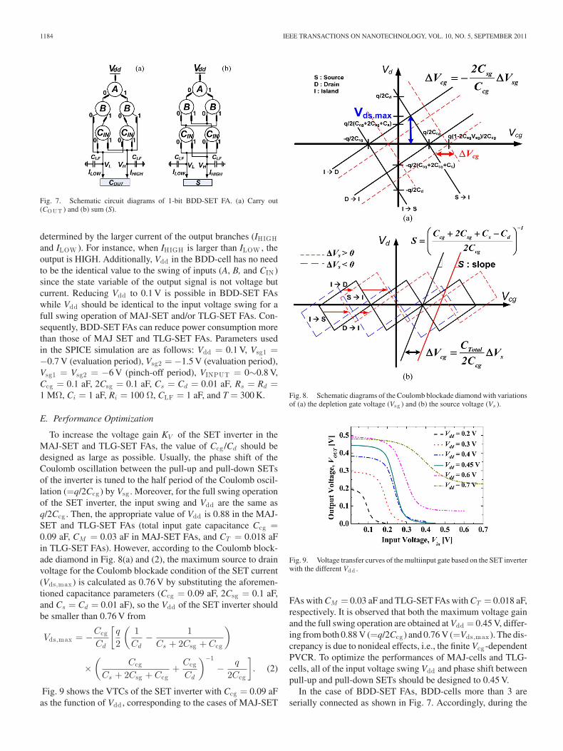
The scheme of processing the inputs and a clock signal canbe diversely optimized corresponding to the various implemen-tation methods of the BDD logic circuits. Fig. 7 shows theproposed BDD-SET FA. Fig. 7(a) and (b) shows COUT and Sof the 1-bit BDD-SET FA, respectively. Both COUT and S are
1184 IEEE TRANSACTIONS ON NANOTECHNOLOGY, VOL. 10, NO. 5, SEPTEMBER 2011
Fig. 7. Schematic circuit diagrams of 1-bit BDD-SET FA. (a) Carry out(COUT ) and (b) sum (S).
determined by the larger current of the output branches (IHIGHand ILOW ). For instance, when IHIGH is larger than ILOW , theoutput is HIGH. Additionally, Vdd in the BDD-cell has no needto be the identical value to the swing of inputs (A, B, and CIN )since the state variable of the output signal is not voltage butcurrent. Reducing Vdd to 0.1 V is possible in BDD-SET FAswhile Vdd should be identical to the input voltage swing for afull swing operation of MAJ-SET and/or TLG-SET FAs. Con-sequently, BDD-SET FAs can reduce power consumption morethan those of MAJ SET and TLG-SET FAs. Parameters usedin the SPICE simulation are as follows: Vdd = 0.1 V, Vsg1 =−0.7 V (evaluation period), Vsg2 = −1.5 V (evaluation period),Vsg1 = Vsg2 = −6 V (pinch-off period), VINPUT = 0∼0.8 V,Ccg = 0.1 aF, 2Csg = 0.1 aF, Cs = Cd = 0.01 aF, Rs = Rd =1 MΩ, Ci = 1 aF, Ri = 100 Ω, CLF = 1 aF, and T = 300 K.
E. Performance Optimization
To increase the voltage gain KV of the SET inverter in theMAJ-SET and TLG-SET FAs, the value of Ccg /Cd should bedesigned as large as possible. Usually, the phase shift of theCoulomb oscillation between the pull-up and pull-down SETsof the inverter is tuned to the half period of the Coulomb oscil-lation (=q/2Ccg ) by Vsg . Moreover, for the full swing operationof the SET inverter, the input swing and Vdd are the same asq/2Ccg . Then, the appropriate value of Vdd is 0.88 in the MAJ-SET and TLG-SET FAs (total input gate capacitance Ccg =0.09 aF, CM = 0.03 aF in MAJ-SET FAs, and CT = 0.018 aFin TLG-SET FAs). However, according to the Coulomb block-ade diamond in Fig. 8(a) and (2), the maximum source to drainvoltage for the Coulomb blockade condition of the SET current(Vds,max ) is calculated as 0.76 V by substituting the aforemen-tioned capacitance parameters (Ccg = 0.09 aF, 2Csg = 0.1 aF,and Cs = Cd = 0.01 aF), so the Vdd of the SET inverter shouldbe smaller than 0.76 V from
Vds,max = −Ccg
Cd
[q
2
(1
Cd− 1
Cs + 2Csg + Ccg
)
×(
Ccg
Cs + 2Csg + Ccg+
Ccg
Cd
)−1
− q
2Ccg
]. (2)
Fig. 9 shows the VTCs of the SET inverter with Ccg = 0.09 aFas the function of Vdd , corresponding to the cases of MAJ-SET
Fig. 8. Schematic diagrams of the Coulomb blockade diamond with variationsof (a) the depletion gate voltage (Vsg ) and (b) the source voltage (Vs ).
Fig. 9. Voltage transfer curves of the multiinput gate based on the SET inverterwith the different Vdd .
FAs with CM = 0.03 aF and TLG-SET FAs with CT = 0.018 aF,respectively. It is observed that both the maximum voltage gainand the full swing operation are obtained at Vdd = 0.45 V, differ-ing from both 0.88 V (=q/2Ccg ) and 0.76 V (=Vds,max ). The dis-crepancy is due to nonideal effects, i.e., the finite Vcg -dependentPVCR. To optimize the performances of MAJ-cells and TLG-cells, all of the input voltage swing Vdd and phase shift betweenpull-up and pull-down SETs should be designed to 0.45 V.
In the case of BDD-SET FAs, BDD-cells more than 3 areserially connected as shown in Fig. 7. Accordingly, during the
LEE et al.: COMPARATIVE STUDY ON ENERGY-EFFICIENCIES OF SINGLE-ELECTRON TRANSISTOR-BASED BINARY FULL ADDERS 1185
Fig. 10. Change of SET current oscillation in Ids –Vgs characteristics by thevariation of Vs in cases of SETs (a) with and (b) without nonideal effects.
adder operation, a change in the source and/or the drain voltage(Vs and/or Vd ) of the SET in each BDD-cell is larger than that ofthe MAJ-SET FA and TLG-SET FA. Fig. 10 illustrates how thecurrent oscillation in the Ids–Vgs characteristic is changed bythe variation of Vs . In BDD-SET FAs, nonideal effects changeof the operating points by Vs and/or Vd .
To optimize BDD-SET FAs, the phase shift of Coulombblockade diamond by both Vsg and Vds should be considered asseen in Fig. 8. Here, the Coulomb blockade diamond consistsof four lines: source to island (S→I), island to source (I→S),drain to island (D→I), and island to drain (I→D). As shown inFig. 8(b), each phase of four lines is shifted by ΔVcg with thechange in ΔVs as follows:
S → I, I → S : ΔVcg =Ccg + 2Csg + Cd
CcgΔVs
D → I, I → D : ΔVcg =Cs
CcgΔVs. (3)
In particular, the lines of S→I and I→S are much more shiftedthan those of D→I and I→D as ΔVs changes. Thus, theCoulomb blockade diamond is shifted not only upward anddownward, but also right and left. Consequently, the position ofthe peak current of the Coulomb oscillation shifts by ΔVcg withthe change in ΔVs and ΔVd as follows:
ΔVcg =Ccg + 2Csg + Cd + Cs
2CcgΔVs =
Ctotal
2CcgΔVs
ΔVcg =Ccg + 2Csg + Cs − Cd
2CcgΔVd (4)
where the position of Coulomb oscillation peak current definedby the center position between S→I and I→D lines on the sameVd as seen in the solid line marked by the slope in Fig. 8(b).In BDD-SET FAs, the value of Ctotal/Ccg should be designedsmall enough to make the position of the Coulomb oscillationpeak current robust to the Vs and Vd variation. Finally, optimizeddevice parameters are summarized in Table II.
IV. SIMULATION RESULTS AND DISCUSSION
Fig. 11(a) shows three inputs of the respective 1-bit SET-based FAs used in the SPICE simulation. The minimum periodof three inputs (A, B, and CIN ) is 1 ns. Each of the risingtime (tr ) and falling time (tf ) of the input voltage VINPUTis 10 ps in Fig. 11(a). The input swing is 0–0.45 V (MAJ-SETand TLG-SET FAs) and 0–0.8 V (BDD-SET FAs). Here, the
TABLE IIOPTIMIZED DEVICE PARAMETERS IN VARIOUS 1-BIT SET-BASED FAS
interconnection RC components of Ci = 1 aF and Ri = 100 Ωare applied as seen in Figs. 4(b), 5(b), and 7.
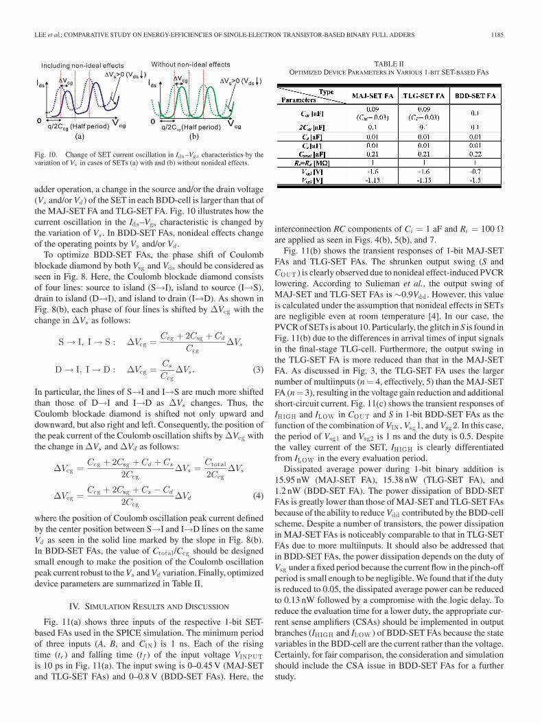
Fig. 11(b) shows the transient responses of 1-bit MAJ-SETFAs and TLG-SET FAs. The shrunken output swing (S andCOUT ) is clearly observed due to nonideal effect-induced PVCRlowering. According to Sulieman et al., the output swing ofMAJ-SET and TLG-SET FAs is ∼0.9Vdd . However, this valueis calculated under the assumption that nonideal effects in SETsare negligible even at room temperature [4]. In our case, thePVCR of SETs is about 10. Particularly, the glitch in S is found inFig. 11(b) due to the differences in arrival times of input signalsin the final-stage TLG-cell. Furthermore, the output swing inthe TLG-SET FA is more reduced than that in the MAJ-SETFA. As discussed in Fig. 3, the TLG-SET FA uses the largernumber of multiinputs (n = 4, effectively, 5) than the MAJ-SETFA (n = 3), resulting in the voltage gain reduction and additionalshort-circuit current. Fig. 11(c) shows the transient responses ofIHIGH and ILOW in COUT and S in 1-bit BDD-SET FAs as thefunction of the combination of VIN , Vsg1, and Vsg2. In this case,the period of Vsg1 and Vsg2 is 1 ns and the duty is 0.5. Despitethe valley current of the SET, IHIGH is clearly differentiatedfrom ILOW in the every evaluation period.
Dissipated average power during 1-bit binary addition is15.95 nW (MAJ-SET FA), 15.38 nW (TLG-SET FA), and1.2 nW (BDD-SET FA). The power dissipation of BDD-SETFAs is greatly lower than those of MAJ-SET and TLG-SET FAsbecause of the ability to reduce Vdd contributed by the BDD-cellscheme. Despite a number of transistors, the power dissipationin MAJ-SET FAs is noticeably comparable to that in TLG-SETFAs due to more multiinputs. It should also be addressed thatin BDD-SET FAs, the power dissipation depends on the duty ofVsg under a fixed period because the current flow in the pinch-offperiod is small enough to be negligible. We found that if the dutyis reduced to 0.05, the dissipated average power can be reducedto 0.13 nW followed by a compromise with the logic delay. Toreduce the evaluation time for a lower duty, the appropriate cur-rent sense amplifiers (CSAs) should be implemented in outputbranches (IHIGH and ILOW ) of BDD-SET FAs because the statevariables in the BDD-cell are the current rather than the voltage.Certainly, for fair comparison, the consideration and simulationshould include the CSA issue in BDD-SET FAs for a furtherstudy.
1186 IEEE TRANSACTIONS ON NANOTECHNOLOGY, VOL. 10, NO. 5, SEPTEMBER 2011
Fig. 11. (a) Three inputs applied in the SPICE simulation. The transient re-sponses of (b) 1-bit MAJ-SET FAs, 1-bit TLG-SET FAs, and (c) BDD-SETFAs.
As shown in Fig. 11(b), the critical path (S) delay is 52 ns(MAJ-SET FAs) and 107 ns (TLG-SET FAs). Because the nodeof COUT BAR in TLG-SET FAs in Fig. 5(b) has the larger fan-out capacitance than those of any other nodes, the switching ofCOUT BAR is much slower than that of A, B, and CIN . Glitchesin the output result from the differences in the arrival times ofinput signals in Fig. 11(b). The critical path delay of BDD-SETFAs, which is defined by the saturation time of VH and VL inFig. 7, is 20 ps.
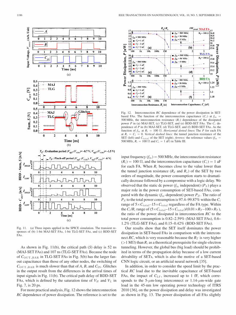
For more practical analysis, Fig. 12 shows the interconnectionRC dependence of power dissipation. The reference is set to the
Fig. 12. Interconnection RC dependence of the power dissipation in SET-based FAs. The function of the interconnection capacitance (Ci ) at fin =500 MHz, the interconnection resistance (Ri ) dependence of the dissipatedpower P in (a) MAJ-SET, (c) TLG-SET, and (e) BDD-SET FAs. The Ci de-pendence of P in (b) MAJ-SET, (d) TLG-SET, and (f) BDD-SET FAs. As thefunction of fin at Ri = 100 Ω. Horizontal dotted lines: The P for each FAat Ri = Ci = 0. Vertical dashed lines: the tunnel junction resistance of theSET (left) and Ctota l of the SET (right). Arrows: the reference values (fin =500 MHz, Ri = 100 Ω and Ci = 1 aF) in Table III.
input frequency (fin ) = 500 MHz, the interconnection resistance(Ri) = 100 Ω, and the interconnection capacitance (Ci) = 1 aFfor each FA. When Ri becomes close to the value lower thanthe tunnel junction resistance (Rd and Rs) of the SET by twoorders of magnitude, the power consumption starts to dramati-cally decrease followed by a compromise with a logic delay. Weobserved that the static dc power (fin independent) (PS ) plays amajor role in the power consumption of SET-based FAs, com-pared with the dynamic (fin -dependent) power PD . The ratio ofPS to the total power consumption is 97.4–99.87% within the Ci
range of 5×Ctotal–15×Ctotal regardless of the FA type. Withinthe Ci /Ri range of (5×Ctotal–15×Ctotal)/(0.01×RT –100×RT ),the ratio of the power dissipated in interconnection RC to thetotal power consumption is 0.82–2.59% (MAJ-SET FAs), 0.6–1.2% (TLG-SET FAs), and 0.15–0.42% (BDD-SET FAs).
Our results show that the SET itself dominates the powerdissipation in SET-based FAs in comparison with the intercon-nect RC, which is very reasonable because the RT is very higher(>1 MΩ) than Ri as a theoretical prerequisite for single-electrontunneling. However, the global bus (big load) should be prohib-ited in terms of the propagation delay because of a low currentdrivability of SETs, which is also the motive of a SET-basedCNN logic circuit, or an artificial neural network [35].
In addition, in order to consider the speed limit by the prac-tical RC load due to the inevitable capacitance of SET-basedFAs, the impact of CLF , increased up to 1 fF, which corre-sponds to the 5-μm-long interconnect or 1.14-μm-wide gateload in the 45-nm low operating power technology of ITRS2010 [36], on the power dissipation and delay was investigatedas shown in Fig. 13. The power dissipation of all FAs slightly

LEE et al.: COMPARATIVE STUDY ON ENERGY-EFFICIENCIES OF SINGLE-ELECTRON TRANSISTOR-BASED BINARY FULL ADDERS 1187
Fig. 13. Fan-out capacitance (CLF ) dependence of the power dissipation anddelay in SET-based FAs.
Fig. 14. Assumed Gaussian distribution of Ccg and Q0 with different As.
increases with CLF . And, the delay of all FAs increases abouta hundredfold as CLF changes from 1 aF to 1 fF. Although allFAs have similar trend according to increase of CLF in termsof power dissipation and delay, the BDD-SET FA still has thelowest power dissipation and delay compared with those of theother.
To assess the sensitivity to a process variation (backgroundcharge noise ΔQ0 and Ccg mismatch ΔCcg ), the Gaussian dis-tribution of background charge (Q0) and Ccg is assumed as seenin Fig. 14, reflecting the level of process technology. We definedA in Fig. 14 as the difference between the mean (Ccg and/or Q0)and the three standard deviations (3-sigma, 3σ). Fig. 14 showstwo different cases of A. In addition, the SPICE Monte Carlosimulation (the number of events = 300) generates the randomvalues which lie within 3σ of the mean under the fixed A for theGaussian distribution. Then, we observed how the adders workwhile increasing A from 0.05 × Ccg to Ccg with a 0.01 × Ccgstep under the fixed mean. For example, if the adder circuit doesnot fail until A is 0.1 × Ccg in the case of Ccg (=1 aF), thenthe maximum allowed mismatch value of ΔCcg is ±0.1 of Ccgto guarantee a normal circuit operation. The maximum allowedmismatch of ΔQ0 is also calculated by this methodology. As weknow, the possibility that the circuit fails increases as the dif-ference between the mean and the generated value gets larger.Therefore, as the allowed A increases, the adder circuits be-come more robust to process variations in perspective of circuitmalfunction.
After ΔCcg was defined as the difference between two SETscomprising the MAJ-cell, TLG-cell, and BDD-cell by the afore-mentioned way, the Monte Carlo simulation based on Lee’sSPICE model was performed with the statistical variation ofQ0 and Ccg of every SET comprising three-type 1-bit FAs(MAJ-SET FAs, TLG-SET FAs, and BDD-SET FAs). Con-sequently, we found that Q0 should be controlled withinthe range of ΔQ0 < ±0.0392q (MAJ-SET FAs), ±0.028q(TLG-SET FAs), and ±0.112q (BDD-SET FAs) to circumvent
TABLE IIICOMPARISON OF PERFORMANCE PARAMETERS IN VARIOUS 1-BIT SET-BASED
FAS INCLUDING NONIDEAL EFFECTS
the malfunction of SET-FAs. Additionally, in terms of the toler-ant range of Ccg mismatch, Ccg ± ΔCcg with ΔCcg < 35% ofCcg (MAJ-SET FAs), 20% of Ccg (TLG-SET FAs), and 50% ofCcg (BDD-SET FAs) are required. These results come from fol-lowing assumptions: the logic threshold for the MAJ-SET andTLG-SET FAs is half of the input voltage swing in the SET in-verters, and logical failure for the BDD-SET FA is defined whenthe amplitude of output signals (IHIGH and ILOW ) is erroneouslyflipped.
Conclusively, the SPICE simulation results including non-ideal effects for 1-bit SET-based FAs are summarized inTable III. Additionally, for assessing the degree of nonideality,the simulation results without nonideal effects are also summa-rized in Table IV. For the ideal case, the TBL and CAL parame-ters (in Table I) were set to be zero. By comparing Table III withTable IV, it is found that all performance parameters are de-graded by ×2–3 due to nonideal effects. Meanwhile, it is notice-able that the SET adder-type dependence is consistent regardlessof nonideality. Remarkably, the dissipated average power andenergy efficiency of BDD-SET FAs are dramatically lower thanthose of MAJ-SET and TLG-SET FAs. Considering the dutyof Vsg (evaluation time)-dependent power consumption, roomfor further power reduction (consequently energy efficiency) re-mains. Furthermore, BDD-SET FAs are superior to MAJ-SETand TLG-SET FAs from the perspective of both the delay andthe robustness to process variations. In contrast, the advantagesof BDD-SET FAs are compromised with the chip density (num-ber of required SETs) and the necessity of CSAs in their I/Ointerfaces.
Finally, it should be noted that the SET adders should becompared with their CMOS counterparts because in this paper,SETs are used as simple MOSFET-like devices to control the
1188 IEEE TRANSACTIONS ON NANOTECHNOLOGY, VOL. 10, NO. 5, SEPTEMBER 2011
TABLE IVCOMPARISON OF PERFORMANCE PARAMETERS IN VARIOUS 1-BIT SET-BASED
FAS WITHOUT NONDEAL EFFECTS (fin = 500 MHz)
Fig. 15. Schematic diagrams of the CMOS BDD-cell.
TABLE VTHE CMOS MODEL PARAMETERS FOR THE BDD-CMOS FAS AND THEIR
TYPICAL VALUES USED IN THE SIMULATION
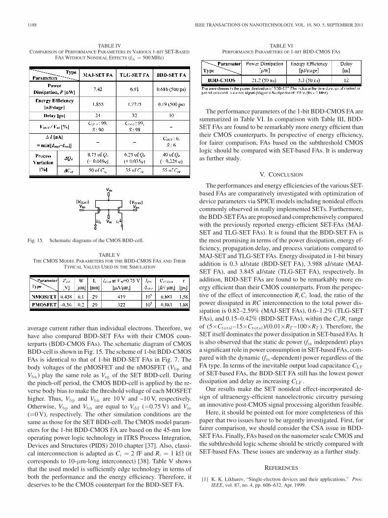
average current rather than individual electrons. Therefore, wehave also compared BDD-SET FAs with their CMOS coun-terparts (BDD-CMOS FAs). The schematic diagram of CMOSBDD-cell is shown in Fig. 15. The scheme of 1-bit BDD-CMOSFAs is identical to that of 1-bit BDD-SET FAs in Fig. 7. Thebody voltages of the pMOSFET and the nMOSFET (Vbp andVbn ) play the same role as Vsg of the SET BDD-cell. Duringthe pinch-off period, the CMOS BDD-cell is applied by the re-verse body bias to make the threshold voltage of each MOSFEThigher. Thus, Vbp and Vbn are 10 V and –10 V, respectively.Otherwise, Vbp and Vbn are equal to Vdd (=0.75 V) and Vss(=0 V), respectively. The other simulation conditions are thesame as those for the SET BDD-cell. The CMOS model param-eters for the 1-bit BDD-CMOS FA are based on the 45-nm lowoperating power logic technology in ITRS Process Integration,Devices and Structures (PIDS) 2010 chapter [37]. Also, classi-cal interconnection is adapted as Ci = 2 fF and Ri = 1 kΩ (itcorresponds to 10-μm-long interconnect) [38]. Table V showsthat the used model is sufficiently edge technology in terms ofboth the performance and the energy efficiency. Therefore, itdeserves to be the CMOS counterpart for the BDD-SET FA.
TABLE VIPERFORMANCE PARAMETERS OF 1-BIT BDD-CMOS FAS
The performance parameters of the 1-bit BDD-CMOS FA aresummarized in Table VI. In comparison with Table III, BDD-SET FAs are found to be remarkably more energy efficient thantheir CMOS counterparts. In perspective of energy efficiency,for fairer comparison, FAs based on the subthreshold CMOSlogic should be compared with SET-based FAs. It is underwayas further study.
V. CONCLUSION
The performances and energy efficiencies of the various SET-based FAs are comparatively investigated with optimization ofdevice parameters via SPICE models including nonideal effectscommonly observed in really implemented SETs. Furthermore,the BDD-SET FAs are proposed and comprehensively comparedwith the previously reported energy-efficient SET-FAs (MAJ-SET and TLG-SET FAs). It is found that the BDD-SET FA isthe most promising in terms of the power dissipation, energy ef-ficiency, propagation delay, and process variations compared toMAJ-SET and TLG-SET FAs. Energy dissipated in 1-bit binaryaddition is 0.3 aJ/state (BDD-SET FA), 3.988 aJ/state (MAJ-SET FA), and 3.845 aJ/state (TLG-SET FA), respectively. Inaddition, BDD-SET FAs are found to be remarkably more en-ergy efficient than their CMOS counterparts. From the perspec-tive of the effect of interconnection RiCi load, the ratio of thepower dissipated in RC interconnection to the total power dis-sipation is 0.82–2.59% (MAJ-SET FAs), 0.6–1.2% (TLG-SETFAs), and 0.15–0.42% (BDD-SET FAs), within the Ci /Ri rangeof (5×Ctotal–15×Ctotal)/(0.01×RT –100×RT ). Therefore, theSET itself dominates the power dissipation in SET-based FAs. Itis also observed that the static dc power (fin independent) playsa significant role in power consumption in SET-based FAs, com-pared with the dynamic (fin -dependent) power regardless of theFA type. In terms of the inevitable output load capacitance CLFof SET-based FAs, the BDD-SET FA still has the lowest powerdissipation and delay as increasing CLF .
Our results make the SET nonideal effect-incorporated de-sign of ultraenergy-efficient nanoelectronic circuitry pursuingan innovative post-CMOS signal processing algorithm feasible.
Here, it should be pointed out for more completeness of thispaper that two issues have to be urgently investigated. First, forfairer comparison, we should consider the CSA issue in BDD-SET FAs. Finally, FAs based on the nanometer scale CMOS andthe subthreshold logic scheme should be strictly compared withSET-based FAs. These issues are underway as a further study.
REFERENCES
[1] K. K. Likharev, “Single-electron devices and their applications,” Proc.IEEE, vol. 87, no. 4, pp. 606–632, Apr. 1999.
LEE et al.: COMPARATIVE STUDY ON ENERGY-EFFICIENCIES OF SINGLE-ELECTRON TRANSISTOR-BASED BINARY FULL ADDERS 1189
[2] S. M. Goodnick and J. Bird, “Quantum-effect and single-electron de-vices,” IEEE Trans. Nanotechnol., vol. 2, no. 4, pp. 368–385, Dec. 2003.
[3] W. Ibrahim, V. Beiu, and M. H. Sulieman, “On the reliability of majoritygates full adders,” IEEE Trans. Nanotechnol., vol. 7, no. 1, pp. 56–67,Jan. 2008.
[4] M. H. Sulieman and V. Beiu, “On single-electron technology full adders,”IEEE Trans. Nanotechnol, vol. 4, no. 6, pp. 669–680, Nov. 2005.
[5] C. Wasshuber, H. Kosina, and S. Selberherr, “SIMON—A simulator forsingle-electron tunnel devices and circuits,” IEEE Trans. Comput.- AidedDesign Integr. Circuits Syst., vol. 16, no. 9, pp. 937–944, Sep. 1997.
[6] K. Uchida, K. Matsuzawa, J. Koga, R. Ohba, S. Takagi, and A. Toriumi,“Analytical single-electron transistor (SET) model for design and analysisof realistic SET circuits,” Jpn. J. Appl. Phys., vol. 39, no. 4B, pp. 2321–2324, Apr. 2000.
[7] S. Mahapatra, A. M. Ionescu, and K. Banerjee, “A quasi-analytical SETmodel for few electron circuit simulation,” IEEE Electron Device Lett.,vol. 23, no. 6, pp. 366–368, Jun. 2002.
[8] S. Mahapatra, V. Vaish, C. Wasshuber, K. Banerjee, and A. M. Ionescu,“Analytical modeling of single electron transistor for hybrid CMOS-SET analog IC design,” IEEE Trans. Electron Devices, vol. 51, no. 11,pp. 1772–1782, Nov. 2004.
[9] H. Inokawa and Y. Takahashi, “A compact analytical model for asymmet-ric single-electron transistors,” IEEE Trans. Electron. Devices, vol. 50,no. 2, pp. 455–461, Feb. 2003.
[10] Y. S. Yu, J. H. Oh, S. W. Hwang, and D. Ahn, “Equivalent circuits approachfor single electron transistor model for efficient circuit simulation bySPICE,” IEEE Electron Device Lett., vol. 38, no. 16, pp. 850–852, Aug.2002.
[11] S. H. Lee, D. H. Kim, K. R. Kim, J. D. Lee, B.-G. Park, Y.-J. Gu, G.-Y. Yang, and J.-T. Kong, “A practical SPICE model based on the physicsand characteristics of realistic single-electron transistors,” IEEE Trans.Nanotechnol., vol. 1, no. 4, pp. 226–232, Dec. 2002.
[12] D. H. Kim, S.-K. Sung, K. R. Kim, J. D. Lee, B.-G. Park, B. H. Choi,S. W. Hwang, and D. Ahn, “Silicon single-electron transistors with side-wall depletion gates and their application to dynamic single-electron tran-sistor logic,” IEEE Trans. Electron Devices, vol. 49, no. 4, pp. 627–635,Apr. 2002.
[13] D. H. Kim, S.-K. Sung, K. R. Kim, J. D. Lee, and B.-G. Park, “Single-electron transistors based on gate-induced Si island for single-electronlogic application,” IEEE Trans. Nanotechnol., vol. 1, no. 4, Dec. pp.170–175, 2002.
[14] A. Fujiwara, H. Inokawa, K. Yamazaki, H. Namatsu, and Y. Takahashi,“Single electron tunneling transistor with tunable barriers using siliconnanowire metal-oxide-semiconductor field-effect transistor,” Appl. Phys.Lett., vol. 88, pp. 053121-1–053121-3, Feb. 2006.
[15] N. M. Zimmerman, A. Fujiwara, H. Inokawa, and Y. Takahashi, “Electro-statically gated Si devices: Coulomb blockade and barrier capacitance,”Appl. Phys. Lett., vol. 89, pp. 052102-1–052102-3, Jul. 2006.
[16] K. W. Song, Y. K. Lee, J. S. Sim, H. Jeoung, J. D. Lee, B.-G. Park, Y.S. Jin, and Y.-W. Kim, “SET/CMOS hybrid process and multiband filteringcircuits,” IEEE Trans. Electron Devices, vol. 52, no. 8, pp. 1845–1850,Aug. 2005.
[17] S. Kang, D. H. Kim, I.-H. Park, J.-H. Kim, J .-E. Lee, J . D. Lee, andB .-G. Park, “Self-aligned dual-gate single-electron transistors,” Jpn. J.Appl. Phys, vol. 47, no. 4, pp. 3118–3122, Apr. 2008.
[18] D. S. Lee, S. Kang, K.-C. Kang, J.-E. Lee, J. H. Lee, K.-J. Song, D. M. Kim,J. D. Lee, and B.-G. Park, “Fabrication and characteristics of self-aligneddual-gate single-electron transistors,” IEEE Trans. Nanotechnol., vol. 8,no. 5, pp. 492–497, Jul. 2009.
[19] Y. C. Jung, K. H. Cho, B. H. Hong, S. H. Son, D. S. Kim, D. Whang,S. W. Hwang, Y. S. Yu, and D. Ahn, “Fabrication and characterizationof sidewall defined silicon-on-insulator single-electron transistor,” IEEETrans. Nanotechnol., vol. 7, no. 5, pp. 544–550, Sep. 2008.
[20] S. Oda and D. Ferry, Silicon Nanoelectronics. Boca Raton, FL: Taylor& Francis, 2006, pp. 23–26.
[21] J.-T. Kong, “CAD for nanometer silicon design challenges and success,”IEEE Trans.Very Large Scale Integr. (VLSI) Syst., vol. 12, no. 11, pp. 1132–1147, Nov. 2004.
[22] S. J. Shin, C. S. Jung, B. J. Park, T. K. Yoon, J. J. Lee, S. J. Kim, J.B. Choi, Y. Takahashi, and D. G. Hasko, “Si-based ultrasmall multiswitch-ing single-electron transistor operating at room-temperature,” Appl. Phys.Lett., vol. 97, pp. 103101-1–103101-3, Sep. 2010.
[23] C. Dubuc, J. Beauvais, and D. Drouin, “A nanodamascene process for ad-vanced single-electron transistor fabrication,” IEEE Trans. Nanotechnol.,vol. 7, no. 1, pp. 68–73, Jan. 2008.
[24] M. A. Rafiq, Z. A. K. Durrani, H. Mizuta, A. Colli, P. Servati, A. C. Ferrari,W. I. Milne, and S. Oda, “Room temperature single electron charging insingle silicon nanochains,” J. Appl. Phys, vol. 103, pp. 053705-1–053705-4, Mar. 2008.
[25] K. Miyaji and T. Hiramoto, “Control of full width at half maximum ofCoulomb oscillation in silicon single-hole transistors at room tempera-ture,” Appl. Phys. Lett, vol. 91, pp. 053509-1–053509-3, Aug. 2007.
[26] A. Fujiwara, H. Inokawa, K. Yamazaki, H. Namatsu, Y. Takahashi, N.M. Zimmerman, and S. B. Martin, “Single electron tunneling transistorwith tunable barriers using silicon nanowire metal-oxide-semiconductorfield-effect transistor,” Appl. Phys. Lett, vol. 88, pp. 053121-1–053121-3,Feb. 2006.
[27] T. Kitade, K. Ohkura, and A. Nakajima, “Room temperature operation ofan exclusive-OR circuit using a highly doped Si single-electron transistor,”Appl. Phys. Lett, vol. 86, pp. 123118-1–123118-3, Mar. 2005.
[28] Y. Ono, A. Fujiwara, K. Nishiguchi, H. Inokawa, and Y. Takahashi, “Ma-nipulation and detection of single electrons for future information pro-cessing,” J. Appl. Phys, vol. 97, pp. 031101-1–031101-19, Jan. 2005.
[29] H. Iwamura, M. Akazawa, and Y. Amemiya, “Single-electron majoritylogic circuits,” IEICE Trans. Electron., vol. E81-C, pp. 42–48, Jan. 1998.
[30] T. Oya, T. Asai, T. Fukui, and Y. Amemiya, “A majority logic device usingan irreversible single-electron box,” IEEE Trans. Nanotechnol., vol. 2,no. 2, pp. 15–22, Mar. 2003.
[31] C. Lageweg, S. Cotofana, and S. Vassiliadis, “A full adder implementationusing SET based linear threshold gates,” in Proc. Int. Conf. Electron.,Circuits Syst, Sep. 2002, pp. 665–668.
[32] C. Choi, J. Lee, S. Park, I.-Y. Chung, C.-J. Kim, B.-G. Park, D. M. Kim,and D. H. Kim, “Comparative study on the energy efficiency of logic gatesbased on single-electron transistor technology,” Semicond. Sci. Technol.,vol. 23, no. 6, pp. 065007-1–065007-11, May 2009.
[33] H.-Q. Zhao, S. Kasai, Y. Shiratori, and T. Hashizume, “Abinary-decision-diagram-based two-bit arithmetic logic unit on a GaAs-based regularnanowire network with hexagonal topology,” Nanotechnology, vol. 20,p. 245203, May 2009.
[34] N. Asahi, M. Akazawa, and Y. Amemiya, “Single-electron logic devicebased on the binary decision diagram,” IEEE Trans. Electron Devices,vol. 44, no. 7, pp. 1109–1116, Jul. 1997.
[35] C. P. Gerousis, S. M. Goodnick, and W. Porod, “Nanoelectronic single-electron transistor circuits and architectures,” Int. J. Circuit. Theory,vol. 32, no. 5, pp. 323–338, Sep. 2004.
[36] International Technology Roadmap for Semiconductors (ITRS). (2010).[Online]. Available: http://public.itrs.net/.
[37] Process Integration, Devices and Structures (PIDS) Chapter in ITRS2010 Updates. (2010). [Online]. Available: http://www.itrs.net/Links/2010ITRS/Home2010.htm
[38] Interconnect Chapter in ITRS 2010 Update. (2010). [Online]. Available:http://www.itrs.net/Links/2010ITRS/2010Update/ToPost/2010Tables_Interconnect_FOCUS_E1_ITRS.xls
Jieun Lee received the B.S. and M.S. degrees fromKookmin University, Seoul, Korea, in 2008 and 2010,respectively, where she is currently working towardthe Ph.D degree in electrical engineering. During theM.S. studies, she has worked on nanoscaled memorydevice including capacitorless 1T DRAM and designand modeling of energy-efficient SET logic circuits.
Her current research interests include design,fabrication, characterization, and modeling of Si-nanowire biosensor devices.
Jung Han Lee (S’07) was born in Seoul, Korea, in1981. He received the B.S. degree from the Depart-ment of Physics, Korea University, Seoul, in 2007.He is currently working toward the Ph.D. degree innanoscience and technology at Seoul National Uni-versity, Korea.
His current research interests include nanoscalesilicon devices, single-electron transistors, and quan-tum devices.
1190 IEEE TRANSACTIONS ON NANOTECHNOLOGY, VOL. 10, NO. 5, SEPTEMBER 2011
In-Young Chung was born in 1970. He received theB.S., M.S., and Ph.D. degrees in electrical engineer-ing from Seoul National University, Seoul, Korea, in1994, 1996, and 2000, respectively.
From 2000 to 2004, he was with the Memory De-sign Team, Memory Division, Samung Electronics,where he designed RAMBUS DRAM interface cir-cuits and analyzed device characteristics. In 2004, hejoined the faculty of the Department of ElectronicEngineering, Gyeongsang National University, Jinju,Korea. Since 2008, he has been with the Depart-
ment of Electronics and Communications Engineering, Kwangwoon Univer-sity, Seoul, as an Associate Professor. His current research interests include newmemory devices and circuits, sensor system design, and biosensor modeling.
Chang-Joon Kim received the B.S. degree in chemi-cal engineering from Korea University, Seoul, Koreain 1990 and then received the M.S. and Ph.D. degreesin chemical engineering from the Korea Advanced In-stitute of Science and Technology, Daejeon, Korea,in 1992 and 2000, respectively.
From February 1992 to August 1995, he was aProcess Engineer in Hanwha Energy Company, Ltd.From February 2002 to January 2004, he was a Re-search Associate in the Department of Chemistry,University of Washington, Seattle, WA, where he
worked on the cloning and characterization of enzymes involved in the biosyn-thesis of secondary metabolites in microorganisms. In 2004, he joined the De-partment of Chemical and Biological Engineering, Gyeongsang National Uni-versity, Jinju, Korea, where he is currently an Associate Professor. His currentresearch interests include enzyme-biofuel cells, redesign of microorganisms bymetabolic engineering, and fermentation process of engineered strains.
Byung-Gook Park (M’90) received the B.S. andM.S. degrees in electronic engineering from SeoulNational University (SNU), Seoul, Korea, in 1982and 1984, respectively, and the Ph.D. degree in elec-trical engineering from Stanford University, Stanford,CA, in 1990.
From 1990 to 1993, he was at the AT&T Bell Lab-oratories, where he contributed to the development of0.1 μm CMOS and its characterization. From 1993to 1994, he was with Texas Instruments, developing0.25 μm CMOS. In 1994, he joined the SNU as an
Assistant Professor in the School of Electrical Engineering (SoEE), where heis currently a Professor. In 2002, he was at Stanford University as a VisitingProfessor, on his sabbatical leave from the SNU. He was leading the Interuni-versity Semiconductor Research Center (ISRC) at SNU as the Director fromJune 2008 to June 2010. Currently, he is researching at Stanford Universityas a Visiting Professor. His current research interests include the design andfabrication of nanoscale CMOS, flash memories, silicon quantum devices, andorganic thin film transistors. He has authored and coauthored more than 580research papers in journals and conferences, and currently holds 34 Korean andseven U.S. patents.
Dr. Park has served as a committee member on several international con-ferences, including the Microprocesses and Nanotechnology, the IEEE Interna-tional Electron Devices Meeting, the International Conference on Solid StateDevices and Materials, and the IEEE Silicon Nanoelectronics Workshop (Tech-nical Program Chair in 2005, General Chair in 2007). Also, he has been servingas an Editor of the IEEE ELECTRON DEVICE LETTERS. He is currently servingas an Executive Director of Institute of Electronics Engineers of Korea (IEEK)and the Board Member of IEEE Seoul Section. He received “Best Teacher”Award from SoEE in 1997, the Doyeon Award for Creative Research fromISRC in 2003, the Haedong Paper Award from IEEK in 2005, and the Educa-tional Award from College of Engineering, SNU, in 2006. Also, he received theHaedong Academic Research Award from IEEK in 2008.
Dong Myong Kim (S’86–M’88) received the B.S.(magna cum laude) and M.S. degrees in electronicsengineering from Seoul National University, Seoul,Korea, in 1986 and 1988, respectively, and the Ph.D.degree in electrical engineering from University ofMinnesota, Twin Cities, in 1993.
From February 1988 to August 1989, he was withthe Division of Electronic Engineering, Korea In-stitute of Science and Technology (KIST), Seoul,where he worked on the characterization and mod-eling of microwave devices and integrated circuits.
Since March 1993, he has been with the School of Electrical Engineering,Kookmin University, Seoul. He has also been serving as a Special Lecturer forSemiconductor Physics and Devices at Samsung Electronics Company, Hwa-sung, Korea, since April 2002. His current research interest includes design, fab-rication, characterization, and modeling of nanostructure silicon devices, thinfilm transistors, bio-sensors, III–V compound semiconductor devices, volatileand nonvolatile memories, and CMOS RF circuits
Dae Hwan Kim (M’08) received the B.S., M.S., andPh.D. degrees in electrical engineering from SeoulNational University, Seoul, Korea, in 1996, 1998, and2002, respectively.
From 2002 to 2005, he was with Samsung Elec-tronics Company, Ltd., Kyung ki-Do, Korea, wherehe contributed to the design and development of 92-nm DDR DRAM and 80-nm DDR2 DRAM. In 2005,he joined the School of Electrical Engineering, Kook-min University, Seoul, where he is currently an Asso-ciate Professor. His current research interests include
fabrication, characterization, modeling, and design of nanoscale CMOS de-vices and circuits, oxide thin film transistors, future memory devices, Si-basedbiosensor devices, energy-efficient nano-ICs, and Si quantum devices and theirapplications.