998 ieee transactions on nanotechnology, … · huawei.com; [email protected]; ......
TRANSCRIPT

998 IEEE TRANSACTIONS ON NANOTECHNOLOGY, VOL. 14, NO. 6, NOVEMBER 2015
An Energy-Efficient Nonvolatile In-MemoryComputing Architecture for Extreme LearningMachine by Domain-Wall Nanowire Devices
Yuhao Wang, Hao Yu, Senior Member, IEEE, Leibin Ni, Guang-Bin Huang, Senior Member, IEEE, Mei Yan,Chuliang Weng, Wei Yang, and Junfeng Zhao
Abstract—The data-oriented applications have introduced in-creased demands on memory capacity and bandwidth, which raisesthe need to rethink the architecture of the current computingplatforms. The logic-in-memory architecture is highly promisingas future logic-memory integration paradigm for high through-put data-driven applications. From memory technology aspect,as one recently introduced nonvolatile memory device, domain-wall nanowire (or race-track) not only shows potential as futurepower efficient memory, but also computing capacity by its uniquephysics of spintronics. This paper explores a novel distributed in-memory computing architecture where most logic functions are ex-ecuted within the memory, which significantly alleviates the band-width congestion issue and improves the energy efficiency. Theproposed distributed in-memory computing architecture is purelybuilt by domain-wall nanowire, i.e., both memory and logic areimplemented by domain-wall nanowire devices. As a case study,neural network-based image resolution enhancement algorithm,called DW-NN, is examined within the proposed architecture. Weshow that all operations involved in machine learning on neuralnetwork can be mapped to a logic-in-memory architecture by non-volatile domain-wall nanowire. Domain-wall nanowire-based logicis customized for in machine learning within image data storage.As such, both neural network training and processing can be per-formed locally within the memory. The experimental results showthat the domain-wall memory can reduce 92% leakage power and16% dynamic power compared to main memory implemented byDRAM; and domain-wall logic can reduce 31% both dynamic and65% leakage power under the similar performance compared toCMOS transistor-based logic. And system throughput in DW-NNis improved by 11.6x and the energy efficiency is improved by 56xwhen compared to conventional image processing system.
Index Terms—Domain wall, extreme learning machine, in-memory computing, nonvolatile memory.
Manuscript received July 20, 2014; revised March 27, 2015; accepted June12, 2015. Date of publication June 19, 2015; date of current version Novem-ber 6, 2015. This work was supported by Singapore NRF-CRP (NRF-CRP9-2011-01), MOE Tier-2 (MOE2010-T2-2-037 (ARC 5/11)), A*STAR PSF fund11201202015 and Huawei Shannon Research Lab. The review of this paper wasarranged by Associate Editor C. A. Moritz.
Y. Wang, H. Yu, L. Ni, G.-B. Huang, and M. Yan are with theSchool of Electrical and Electronic Engineering, Nanyang TechnologicalUniversity, 639798 Singapore (e-mail: [email protected]; [email protected]; [email protected]; [email protected]; [email protected]).
C. Weng, W. Yang and J. Zhao are with Shannon Laboratory, HuaweiTechnologies Co., Ltd., Hangzhou, 310051 China (e-mail: [email protected]; [email protected]; [email protected]).
Color versions of one or more of the figures in this paper are available onlineat http://ieeexplore.ieee.org.
Digital Object Identifier 10.1109/TNANO.2015.2447531
I. INTRODUCTION
THE analysis of big-data at exascale (1018 bytes/s or flops)has introduced the emerging need to reexamine the exist-
ing hardware platform that can support memory-oriented com-puting. A big-data-driven application requires huge bandwidthwith maintained low-power density. The most widely existeddata-driven application is machine learning in big data storagesystem, as the most exciting feature of future big-data storagesystem is to find implicit pattern of data and excavate valuedbehavior behind. Take image searching as an example, insteadof performing the image search by calculating pixel similarity,image search by machine learning is a similar process as humanbrains, which learns the features of all images by feature extrac-tion algorithms and compares the features in the form of strings.As such, the image search becomes a traditional string matchingproblem which is much easier to solve. However, to handle bigimage data at exa-scale, there is a memory wall that has longmemory access latency as well as limited memory bandwidth.Again take the example of image search in one big-data storagesystem, there may be billions of images, so that to perform fea-ture extraction for all images will lead to significant congestionat I/Os when migrating data between memory and processor. Inaddition, the large volume of memory will experience signifi-cant leakage power, especially at advanced CMOS technologynodes, for holding data in volatile memory for fast accesses[1], [2].
From memory technology point of view, there are many re-cent explorations by the emerging non-volatile memory (NVM)technologies at nano-scale such as phase-change memory, spin-transfer torque memory (STT-RAM), and resistive memory(ReRAM) [3]–[7]. The primary advantage of NVM is the poten-tial as the universal memory with significantly reduced leakagepower. For example, STT-RAM is considered as the second-generation of spin-based memory, which has sub-nanosecondmagnetization switching time and sub-pJ switching energy [8]–[10]. As the third-generation of spin-based memory, domain-wall nanowire, also known as racetrack memory [11], [12],is a newly introduced NVM device that can have multiple bitsdensely packed in one single nanowire, where each bit can be ac-cessed by the manipulation of the domain-wall. Compared withSTT-RAM, the domain-wall nanowire is able to provide the sim-ilar speed and power but with much higher density or through-put [13]. Since domain-wall nanowire has close-to-DRAM den-sity but with close-to-zero standby power, it becomes an ideal
1536-125X © 2015 IEEE. Personal use is permitted, but republication/redistribution requires IEEE permission.See http://www.ieee.org/publications standards/publications/rights/index.html for more information.

WANG et al.: ENERGY-EFFICIENT NONVOLATILE IN-MEMORY COMPUTING ARCHITECTURE FOR EXTREME LEARNING MACHINE 999
candidate for future main memory that can be utilized for big-data processing.
From architecture point of view, the logic-in-memory ar-chitecture is introduced to overcome memory bandwidth issue[14]–[18]. The basic idea behind is that, instead of feeding pro-cessor large volume of raw data, it is beneficial to preprocessthe data and provide processor only intermediate result. In otherwords, the key is to lower communication traffic by operandsreduction. For example, to perform a sum of ten numbers, in-stead of transmitting ten numbers to processor, in-memory ar-chitecture is able to obtain the sum by in-memory logic andtransmit only one result thus reduce traffic by 90%. To per-form in-memory logic, it is necessary to implement logic insidememory so that preprocessing logic can be done. However, thein-memory logic circuits in current approaches are composedof CMOS transistors, which are usually made simple otherwisethe power and area overhead would be overwhelming. Interest-ingly, domain-wall nanowire device not only has the potentialfor high density and high performance memory design, but alsointeresting computing capability due to spin-physics. Therefore,it is very promising to implement an in-memory architecturewith both non-volatile domain-wall memory and non-volatilein-memory logic. Such memory based in-memory logic mayovercome the functionality limit of transistor based ones.
However, currently there is no in-depth study to exploredomain-wall nanowire based in-memory computing architec-ture. For example, no link has been made to perform big-datalogic operation based on spin-based device such as domain-wall nanowire. What is more, no domain-wall nanowire devicemodel has been developed in terms of accuracy and efficiencyfor circuit designs. In this paper, the image processing algorithmby neural network learning is examined within the domain-wallnanowire based in-memory architecture. The contributions ofthis work are: firstly, a SPICE behavioral model of domain-wall nanowire has been developed for circuit-level verificationof both memory and logic designs; secondly, the domain-wallmemory has been explored as low power main memory; thirdly,we show that physics of spintronics of domain-wall nanowirecan introduce unique capability to perform logic operationssuch as XOR and addition which other NVM devices do nothave; lastly, a purely domain-wall memory based distributed in-memory computing architecture is proposed, and we show thefeasibility of mapping the ELM neural network to the proposedarchitecture, called DW-NN. The numerical experiments showthat, the domain-wall memory can reduce 92% leakage powerand 16% dynamic power compared to main memory imple-mented by DRAM; and domain-wall logic can reduce 31% bothdynamic and 65% leakage power under the similar performancecompared to CMOS transistor based logic. And compared to thescenario that ELM is executed in CMOS based general purposeprocessor, the proposed DW-NN improves the system through-put by 11.6x and energy efficiency by 56x.
The rest of this paper is organized in the following man-ner. Section II describes the overall in-memory computing plat-form based on domain-wall nanowire. Section III discusses thephysics and SPICE model of domain-wall nanowire. SectionIV details the main memory design by domain-wall nanowire.
Section V presents the domain-wall XOR, addition, and gen-eral LUT by domain-wall nanowire. Section VI introduces themapping of machine learning based super-resolution algorithmon the proposed distributed in-memory architecture. Experi-mental results are presented in Section VII with conclusion inSection VIII.
II. NONVOLATILE IN-MEMORY COMPUTING PLATFORM
Conventionally, all the data is maintained within memorythat is separated from the processor but connected with I/Os.Therefore, during the execution, all data needs to be migratedto processor and written back afterwards. In the data-orientedapplications, however, this will incur significant I/O congestionsand hence greatly degrade the overall performance. In addition,significant standby power will be consumed in order to hold thelarge volume of data.
Theoretically, it is feasible to overcome the bandwidth issueby adding more I/O pins or operating them at higher frequency.Practically, however, the I/O frequency is limited by the signalpropagation delay and signal integrity issues, and I/O num-ber is limited by the packaging technology, thus the bandwidthcan hardly get further improved. Instead of improving memorybandwidth, it is also possible to reduce the required data commu-nication traffic between memory and processor. The basic ideabehind is that, instead of feeding processor large volume of rawdata, it is beneficial to preprocess the data and provide processoronly intermediate result. The key to lower communication traf-fic is the operands reduction. For example, to perform a sum often numbers, instead of transmitting ten numbers to processor,in-memory architecture is able to obtain the sum by in-memorylogic and transmit only one result thus reduce traffic by 90%.To perform in-memory logic, it is necessary to implement logicinside memory so that preprocessing logic can be done. Sucharchitecture is called logic-in-memory architecture. Consider-ing the leakage reduction at the same time, logic-in-memoryarchitectures that are associated with NVM are presented in[14]–[17], [19]. Fig. 1 shows logic in memory architecture atmemory cell level. The example illustrated here is an in-memoryfull adder with both sum logic and carry logic.
The basic circuitry, including access transistor, the word-lineand bit-lines, is to ensure memory access. The data is stored inNVM devices which have either low or high resistance. Redun-dant data is required for each bit of data for logic purpose. Com-binational logic circuit is added inside which the non-volatiledevices are equivalent to transistors: considered turned on ifat low resistance state or turned off if at high resistance state.In such architecture, the desired result can be obtained imme-diately without reading operands as if the results are alreadystored in data array and it is just be ‘readout’. This is very usefulfor some specific applications as this architecture is able to pre-process data without loading data to processor with extremelyshort latency.
As the logic is inserted to one cell or a few cells, it is lim-ited to small size thus cannot be made complex. Usually onlysimple logic is suitable for such architecture otherwise the over-head would be overwhelming. Though simple logic in such

1000 IEEE TRANSACTIONS ON NANOTECHNOLOGY, VOL. 14, NO. 6, NOVEMBER 2015
Fig. 1. In-memory computing architecture at memory cell level.
architecture is able to share the workload of processor, its ef-fect to reduce communication traffic is not obvious due to lim-ited operands reduction. In addition, similar to the operationof memory, for the whole data array only a few logic can beactive concurrently at one time. This leads many logic circuitsto be idle at most of the time, which is not only a waste of com-putational resources but also incurs leakage power for CMOSlogic. Another disadvantage is that the data needs to be storedin a very strict manner, determined by in-memory logic circuitfunctionality.
An alternative in-memory architecture we are presenting atblock level in distributed fashion is illustrated in Fig. 2, whichis more effective for traffic reduction. A memory data is usuallyorganized in H-tree fashion, and the data block can be the dataarray or a number of data arrays that belong to same ‘H-tree’branch. Instead of inserting in-memory logic at memory celllevel inside the data array, the architecture in Fig. 2 pairs eachblock of data with in-memory logic (accelerators). Differentfrom the cell level in-memory architecture, the accelerators canbe made with higher complexity, and the number of acceleratorsfor each data block can also be customized. The data flow ofthe block level in-memory architecture is to readout data fromdata block to in-memory logic, which performs particular func-tionality and then writes back the result. The data also needsto be stored in assigned blocks but it is much more flexiblethan that of cell level in-memory architecture. The block levelin-memory architecture is very effective to reduce communi-cation traffic between memory and processor. This is becausesignificant operands reduction can be achieved by deployingaccelerator with high level functionality. For example, for face
Fig. 2. In-memory computing architecture at memory block level.
recognition in image processing application, instead of trans-mitting a whole image to obtain a Boolean result, the result canbe directly gained through in-memory logic. In other words,the block level in-memory architecture is suitable for big datadriven applications where traffic reduction is more importantthan latency reduction.
In this platform, the domain-wall nanowire is intensivelyused. Both the memory block and logic block in each pair arepurely implemented by domain-wall nanowire devices. In ad-dition, energy efficient domain-wall logic units are deployed inthe external processor to execute instructions that cannot be ac-celerated by in-memory logic. The domain-wall memory designwill be discussed in details in Section IV, and domain-wall logicdesign will be presented in Section V.
III. DEVICE MODEL AND SIMULATION
OF DOMAIN-WALL NANOWIRE
Domain-wall nanowire, also known as racetrack memory[11], [13], [20], is a newly introduced NVM device in whichmultiple bits of information are stored in single ferromagneticnanowire. As shown in Fig. 3(a), each bit is denoted by the left-ward or rightward magnetization direction, and adjacent bits areseparated by domain walls. By applying a current through theshift port at the two ends of the nanowire, all the domain wallswill move left or right at the same velocity while the domainwidth of each bit remains unchanged, thus the stored informa-tion is preserved. Such a tape-like operation will shift all thebits similarly like a shift register.
In order to access the information stored in the domains,a strongly magnetized ferromagnetic layer is placed at desiredposition of the ferromagnetic nanowire and is separated by an in-sulator layer. Such a sandwich-like structure forms a magnetic-tunnel-junction (MTJ), through which the stored informationcan be accessed. In the following, the write, read and shift op-erations are modeled respectively.

WANG et al.: ENERGY-EFFICIENT NONVOLATILE IN-MEMORY COMPUTING ARCHITECTURE FOR EXTREME LEARNING MACHINE 1001
Fig. 3. (a) Schematic of domain-wall nanowire structure with access port andshift port; (b) magnetization of free-layer in spherical coordinates with definedmagnetization angles; and (c) typical R-V curve for MTJ.
A. Magnetization Reversal
The write access can be modeled as the magnetization reversalof MTJ free layer, i.e. the target domain of the nanowire. Notethat the dynamics of magnetization reversal can be described bythe precession of normalized magnetization m, or state variablesθ and φ in spherical coordinates as shown in Fig. 3(b). The spin-current induced magnetization dynamics described by θ and φis given by [21]
θ = θ0Exp(− t
t0
)· cos(φ) (1)
ω =dφ
dt= k1
√k2 − (k3 − k4I)2 (2)
where θ0 is the initial value of θ, slightly tilted from the stable xor −x directions; t0 is procession time constant; ω is the angularspeed of φ; k1 to k4 are magnetic parameters with detailedexplanation in [21]; and I is the spin-current that causes themagnetization precession.
B. Magnetic-Tunnel-Junction Resistance
A typical R-V curve for MTJ is shown in Fig. 3(c) with tworegions: giant magnetoresistance (GMR) region and tunnelingregion. Depending on the alignment of magnetization directionsof the fixed layer and free layer, parallel or anti-parallel, the MTJexhibits two resistance values Rl and Rh . As such, the generalMTJ resistance can be calculated by the giant magnetoresistance(GMR) effect
R(θu , θb) = Rl0 +Rh0 − Rl0
2(1 − cos(θu − θb)) (3)
where θu and θb are the magnetization angles of upper free layerand bottom fixed layer, Rl0 and Rh0 are the MTJ resistanceswhen the applied voltage is subtle. When the applied voltageincreases, there exists tunneling effect caused voltage-dependent
resistance roll-off,⎧⎪⎪⎨
⎪⎪⎩
Rl(V ) =Rl0
1 + clV 2
Rh(V ) =Rh0
1 + chV 2
(4)
where cl and ch are voltage-dependent coefficients for parallelstate and anti-parallel states, respectively.
C. Domain-Wall Propagation
Like a shift register, the domain-wall nanowire shifts in a dig-ital manner, thus could be digitalized and modeled in the unit ofdomains, in which a bit is stored. The magnetization orientationsin adjacent domains can be either parallel or anti-parallel, and themagnetization transition occurs in the connecting domain-wallin case of anti-parallel neighboring bits. Therefore, a domainplus a domain-wall are the basic unit for the shift-operation.Note that except the bit in the MTJ, the other bits denoted bythe magnetization directions are only affected by their adjacentbits. In other words, the magnetization of each bit is controlledby the magnetization in adjacent domains. Inspired by this, wepresent a magnetization controlled magnetization (MCM) de-vices based behavioral model for domain-wall nanowires. Un-like the current-controlled and voltage-controlled devices, thecontrol in MCM device needs to be triggered by rising edge ofone shift (SHF) signal, which can be formulated as
θ = f (Tsl , θr , Tsr , θl , θc) = Tslθr + Tsrθl + T slT srθ0 .(5)
In which Tsl and Tsr are the shift-left and shift-right commands;θr and θl are the magnetization angles in right adjacent cell andleft adjacent cell respectively; θc is the current state before thetrigger signal. This describes that the θ-state will change whentriggered and will remain state if no shift-signal is issued.
For the bit in MTJ, the applied voltage for spin-based readand write will also determine the θ-state as discussed previously.Therefore we have,
θ = f(Tsl , θr , Tsr , θl , θ0) + g(V p, V n, θc) (6)
where V p and V n are the MTJ positive and negative nodalvoltages, and g(V p, V n, θ0) is the additional term that combinesEquation (1) to (4).
In addition, the domain-wall propagation velocity can bemimicked by the SHF-request frequency. The link between theSHF-request frequency and the propagation velocity is the ex-perimentally observed by current-velocity relation [22],
v = k(J − J0), (7)
where J is the injected current density and J0 is the criticalcurrent density.
By combining equations (1) to (6) together, with the mag-netization angles θ and φ as internal state variables other thanelectrical voltages and currents, one can fully describe the be-haviors of the domain-wall nanowire device, where each domainis modeled as the proposed MCM device. As such, the modifiednodal analysis (MNA) can be built in the SPICE-like simulator

1002 IEEE TRANSACTIONS ON NANOTECHNOLOGY, VOL. 14, NO. 6, NOVEMBER 2015
Fig. 4. Macro-cell of DWM with: (a) single access-port; and (b) multipleaccess-ports.
[23], [24] to verify circuit designs by domain-wall nanowiredevices.
IV. DOMAIN-WALL NANOWIRE BASED MAIN MEMORY
Compared with the conventional SRAM or DRAM byCMOS, the domain-wall nanowire based memory (DWM) candemonstrate two major advantages. Firstly, extremely high in-tegration density can be achieved since multiple bits can bepacked in one macro-cell. Secondly, significant standby powerreduction can be expected as a non-volatile device does not re-quire to be powered to retain the stored data. In this section,we will present DWM-based design with macro-cell memory:structure, modeling, and data organization.
A. Domain-Wall Memory Macro-Cell Design
Fig. 4(a) shows the design of domain-wall nanowire basedmemory (DWM) macro-cell with access transistors. The access-port lies in the middle of the nanowire, which divides thenanowire into two segments. The left-half segment of nanowireis used for data storage while the right-half segment is reservedfor shift-operation in order to avoid information lost. For theworst case scenario, in order to access the left-most bit of datasegment, all information in data segment is shift to reservedsegment with first bit aligned with access port. Without re-served segment the magnetization will move beyond the physi-cal boundary and data will get lost. The idea behind is to providetemporary room, while the data in reserved segment are not im-portant. In the worst case scenario discussed above, the reservedsegment has to be at least as long as data segment. In such case,the data utilization rate is only 50%. In order to improve the datautilization rate, a multiple port macro-cell structure is presentedin Fig. 4(b). The access-ports are equally distributed along thenanowire, which divides the nanowire into multiple segments.
Fig. 5. Domain-wall memory read sensing circuit.
Except the right-most segment, all other segments are data seg-ments with the bits in one segment form a group. In such case,to access arbitrary bit in the nanowire, the shift-offset is alwaysless than the length of one segment, thus the data access can bedone faster. As a moderate number of access-ports will be help-ful to increase the data utilization rate, too many access-portsmay lead to the opposite. This is because additional access-portswill incur area overhead to accommodate its access transistors.
The common read sensing circuit for DWM is shown in Fig. 5.To differentiate the high/low resistance values of MTJ in DWM,the reference cell has the resistance of RAP ||RP [25]. Duringthe read operation, the Rd EN is enabled, and bit-line (BL)is applied with read voltage that is less than threshold voltagefor write operation. The current of MTJ branch will be mir-rored to the reference cell branch, and the according voltagesare compared by the sense amplifier (SA), which are two cross-coupled inverters. The write is performed by controlling polarityof write voltage between BL and BLB and asserting the accord-ing WL. In particular, when BL is high and BLB low, parallelor low-resistance state will be written to the MTJ; on the otherhand, BL low and BLB high will result in anti-parallel or high-resistance state of MTJ. The selection of both cell and accessport is achieved through word-line (WL). The number of sens-ing circuit for DWM depends on the width of bits to output, andsensing circuits are shared among different bit-lines by columnmultiplex [13], [26], [27].
The number of bits in one macro-cell can be calculated by
Ncell−bits = (Nrw−ports + 1)Ngroup−bits (8)
In which Nrw−ports is the number of access ports. Then themacro-cell area can be calculated by
Ananowire = Ncell−bitsLbitWnanowire (9)
Acell = Ananowire + 2Ashf−nmos
+ 2Arw−nmosNrw−ports (10)
where Lbit is the pitch size between two consecutive bits,Wnanowire the width of domain-wall nanowire, Ashf−nmos andArw−nmos are the transistor size at shift-port and access-portrespectively.
Moreover, the bit-line capacitance is crucial in the calcu-lation of latency and dynamic power. The increased bit-line

WANG et al.: ENERGY-EFFICIENT NONVOLATILE IN-MEMORY COMPUTING ARCHITECTURE FOR EXTREME LEARNING MACHINE 1003
capacitance due to the multiple access-ports can be obtained by
Cbit−line = (Nrw−portsCdrain−rw
+ Cdrain−shf + Cbl−metal) × Nrow (11)
in which Cbl−metal is the capacitance of bit-line metal wire percell, the Cdrain−rw and Cdrain−shf are the access-port and shift-port transistor drain capacitances, respectively. Note that theundesired increase of per-cell capacitance will be suppressed bythe reduced number of rows due to higher nanowire utilizationrate.
Besides the latency and energy on bit-line and sensing circuit,the domain-wall nanowire specific behaviors will also incur in-cell delay and energy dissipation. The magnetization reversalenergy 0.27pJ and delay 600ps can be obtained through thetransient analysis by the SPICE-like simulation as discussed inSection III. The read-energy is a few fJ. Also, the read-operationwill not contribute in-cell delay. The delay of shift-operation canbe calculated by
Tshift = Lbit/vprop (12)
in which vprop is the domain-wall propagation velocity thatcan be calculated by Equation (7). The Joule heat caused bythe injected current is calculated as the shift-operation dynamicenergy.
B. Cluster-Group Data Organization
There are two potential problems for the DWM macro-cell.Firstly, there exists variable access latencies for the bits thatlocate at different positions in the nanowire. Secondly, if therequired bits are all stored in the same nanowire, very longaccess latency will be incurred due to the sequential access.
It is important to note that the data exchange between mainmemory and cache is always in the unit of a cache-line size ofdata, i.e. the main memory will be read-accessed when last-levelcache miss occurs; and will be write-accessed when a cache-lineneeds to be evicted. Therefore, instead of the per access latency,the latency of the data block in the size of a cache-line becomesthe main concern. Based on such fact, we present a cluster-group based data organization. The idea behind cluster is todistribute data in different nanowires thus they can be accessedin parallel to avoid the sequential access; and the idea behindgroup is to discard the within-group addressing, and transfer theNgroup−bits bits in Ngroup−bits consecutive cycles, to avoid thevariable latency. Specifically, a cluster is the bundle of domain-wall nanowires that can be selected together through bit-linemultiplexers. The number of nanowires in one cluster equalsthe I/O bus bandwidth of the memory. Note that the data in onecache-line have consecutive addresses. Thus, by distributing thebits of N consecutive bytes, where N is decided by the I/O busbandwidth, into different nanowire within a cluster, the requiredN bytes can be accessed in parallel to avoid the sequentialaccess. In addition, within each nanowire in the cluster, the datawill be accessed in the unit of group, i.e. the bits in each groupwill be accessed in consecutive cycles with a similar fashion asDRAM.
Fig. 6. Low power XOR-logic implemented by two domain-wall nanowires.
The number of groups per nanowire is thus decided by
Ngroup−bits = Nline−bits/Nbus−bits . (13)
For example, in system with cache-line size of 64-byte, andmemory I/O bus bandwidth of 64-bit, the group size is 8-bit. Assuch, the DWM with cluster-group based data organization canbe operated in the following steps:
• Step1: The group-head initially is aligned with the access-port, thus the distributed first 8 consecutive bytes can be firsttransferred between memory and cache;
• Step2: Shift the nanowire with 1-bit offset, and transfer thefollowing 8 consecutive bytes. Iterate this step 6 more timesuntil the whole cache-line data is transferred;
• Step3: After the data transfer is completed, the group-head isrelocated to the initial position as required in step 1.
As mentioned in Section III-C, the current-controlled domain-wall propagation velocity is proportional to the applied shift-current,. By applying a larger shift-current, a fast one-cyclecluster head relocation can be achieved. In such a manner, thedata-transfer of cache block will be able to achieve a fixed andalso lowest possible latency.
V. DOMAIN-WALL NANOWIRE BASED LOGIC
The magnetization switching with sub-nanosecond speed andand sub-pJ energy have been experimentally demonstrated [8]–[10]. As such, the domain-wall logic can be further explored forlogic-in-memory based computing. In this section, we show howto further build domain-wall XOR logic, and how it is applied forlow-power ALU design for comparison and addition operations.
A. Domain-Wall XOR Logic
The GMR-effect can be interpreted as the bitwise-XOR op-eration of the magnetization directions of two thin magneticlayers, where the output is denoted by high or low resistance.In a GMR-based MTJ structure, however, the XOR-logic willfail as there is only one operand as variable since the magneti-zation in fixed layer is constant. Nevertheless, this problem canbe overcome by the unique domain-wall shift-operation in thedomain-wall nanowire device, which enables the possibility ofdomain-wall XOR logic for computing.
A bitwise-XOR logic implemented by two domain-wallnanowires is shown in Fig. 6. The proposed bitwise-XOR logic isperformed by constructing a new read-only-port, where two free

1004 IEEE TRANSACTIONS ON NANOTECHNOLOGY, VOL. 14, NO. 6, NOVEMBER 2015
Fig. 7. Carry logic achieved by domain-wall nanowires.
layers and one insulator layer are stacked. The two free layersare in the size of one magnetization domain and are from tworespective nanowires. Thus, the two operands, denoted as themagnetization direction in free layer, can both be variables withvalues assigned through the MTJ of the according nanowire.As such, it can be shifted to the operating port such that theXOR-logic is performed.
For example, the A ⊕ B can be executed in the followingsteps
• The operands A and B are loaded into two nanowires byenabling WL1 and WL2 respectively;
• A and B are shifted from their access-ports to the read-only-ports by enabling SHF1 and SHF2 respectively;
• By enabling RD, the bitwise-XOR result can be obtainedthrough the GMR-effect.
Note that in the x86 architecture processors, most XOR in-structions also need a few cycles to load its operands before thelogic is performed, unless the two operands are both in registers.As such, the proposed domain-wall XOR logic can be a potentialsubstitution of the CMOS-based XOR-logic. Moreover, similaras the DWM macro-cell, zero leakage can be achieved for suchXOR-logic.
B. Domain-Wall Adder
To realize a full adder, one needs both sum logic and carrylogic. As the domain-wall nanowire based XOR logic has beenachieved, the sum logic can be readily realized by deployingtwo units: Sum = (A ⊕ B) ⊕ C. As for carry logic, spintronicsbased carry operation is proposed in [28], where a pre-chargesensing amplifier (PCSA) is used for resistance comparison.The carry logic by PCSA and two branches of domain-wallnanowires is shown in Fig. 7(a). The three operands for carryoperation are denoted by resistance of MTJ (low for 0 and highfor 1), and belong to respective domain-wall nanowires in theleft branch. The right branch is made complementary to the leftone. Note that the Cout and Cout will be pre-charged high at firstwhen PCSA EN signal is low. The complementary values canbe easily obtained by reversely placing the fixed layers of MTJs
Fig. 8. Sum logic achieved by domain-wall nanowires.
in the right branch. When the circuit is enabled, the branch withlower resistance will discharge its output to ‘0’. For example,when left branch has no or only one MTJ in high resistance, i.e.no carry out, the right branch will have three or two MTJs inhigh resistance, such that the Cout will be 0. The complete truthtable is shown in Fig. 7(b), which is able to confirm carry logicby this circuit. The domain-wall nanowire works as the writingcircuit for the operands by writing values at one end and shift itto PCSA. The sum logic of two operands by PCSA is shown inFig. 8.
Together with CARRY logic, the domain-wall based half-adder can be implemented. By deploying two half-adders inseries the domain-wall based full-adder can be achieved. Notethat the domain-wall logic is sequential thus the full-adder isexpected to have longer latency. We will show that the undesiredlong latency can be overcome by the MapReduce based matrixmultiplication in Section VI-C.
C. Domain-Wall Multiplication
With the full adder implemented by domain-wall nanowiresand intrinsic shift ability of domain-wall nanowire, the multipli-cation operation can be easily achieved by breaking it down tomultiple domain-wall shift operations and additions. OperandA with m non-zero bits multiplied by operand B with n non-zero bits (m > n) can be decomposed into n shift operationsand n additions. For example, multiplication of binary 1011and 110 can be decomposed into addition of 10110 and 101100,where 10110 and 101100 are obtained by left-shifting 1011 oneand two bits in domain-wall nanowire. As such, not only canthe complicated domain-wall multiplier circuit be avoided, butalso multiplication operation can be handled more efficiently byreusing domain-wall adders in a distributed MapReduce fashion,which will be discussed in Section VI.
D. Domain-Wall LUT Logic
Look-up table (LUT), essentially a pre-configured memoryarray, takes a binary address as input, finds target cells that con-tain result through decoders, and finally outputs correspondinglyby sense amplifiers. A domain-wall nanowire based LUT is il-lustrated in Fig. 9. Compared with the conventional SRAM orDRAM by CMOS, the domain-wall LUT has higher density andlower leakage power.

WANG et al.: ENERGY-EFFICIENT NONVOLATILE IN-MEMORY COMPUTING ARCHITECTURE FOR EXTREME LEARNING MACHINE 1005
Fig. 9. Domain-wall LUT logic by domain-wall memory array.
Based on the way data is organized, the result can be output insequential manner or parallel manner. In sequential output sce-nario, the binary result is stored in single domain-wall nanowirethat is able to hold multiple bits of information. Assume eachcell has only one access port and the first bit of result is initiallyaligned with access port, the way to output result is to iterativelyreadout and shift one bit until the last bit is output. In paralleloutput scenario, the multiple-bit result is distributed into differ-ent nanowires. Because each cell has their own access port, themultiple bits can be output concurrently. The design complexityof parallel output scheme is that, to find the relative position ofthe result within the nanowire, a variable access time will beintroduced. For example, if the result is stored at first bit of thenanowires, the result can be readout in one cycle; on the contraryif the result is kept at the very last bit of the nanowires, it willtake tens of cycles to shift first before the result is output. There-fore, the choice between sequential output and parallel outputis the tradeoff between access latency and design complexity.
VI. IN-MEMORY MACHINE LEARNING FOR IMAGE PROCESSING
In this section, we will use the extreme learning machinebased super-resolution (ELM-SR) as a case study application,to show how machine learning algorithms can be efficientlyexecuted within the proposed distributed in-memory comput-ing platform. The application of ELM for image processingin this paper is an ELM based image super-resolution (SR)algorithm [29], which learns the image features of a specificcategory of images and improves low-resolution figures by ap-plying learned knowledge. As demonstrated in Section V, we areable to achieve fundamental addition, multiplication, and LUTdomain-wall logic. In the following, we will demonstrate how tomap ELM-SR algorithm to the proposed distributed in-memoryarchitecture.
A. Extreme Learning Machine
Among numerous machine learning algorithms [30]–[34],support vector machine (SVM) [30], [31] and neural network
Fig. 10. Working flow of extreme learning machine.
(NN) [32], [33] are widely discussed. However, both two algo-rithms have major challenging issues in terms of slow learningspeed, trivial human intervene (parameter tuning) and poor com-putational scalability [34]. Extreme Learning Machine (ELM)was initially proposed [34], [35] for the single-hidden-layerfeed-forward neural networks (SLFNs). Compared with tradi-tional neural networks, ELM eliminates the need of parametertuning in the training stage and hence reduces the training timesignificantly. The output function of ELM is formulated as (onlyone output node is considered)
fL =L∑
i=1
βihi (X) = h (X) β (14)
where β = [β1 ,β2 , · · · ,βL ]T is the output weight vector stor-ing the output weights between the hidden layer and outputnode. h (X) = [h1 (X) , h2 (X) , · · · , hL (X)]T is the hiddenlayer output matrix given input vector X and performs the trans-formation of input vector into L-dimensional feature space. Thetraining process of ELM aims to obtain output weight vector βand minimize the training error as well as the norm of outputweight
Minimize : ∥Hβ − T∥ and ∥β∥ (15)
β = H†T (16)
where H† is the Moore-Penrose generalized inverse of matrixH.
Note that ELM-SR is commonly used as pre-processing stageto improve image quality before applying other image algo-rithms. It involves intensive matrix operation, such as matrixaddition, matrix multiplication as well as exponentiation on eachelement of a matrix. Fig. 10 illustrates the computation flow forELM-SR, where input vector obtained from input image is mul-tiplied by input weight matrix. The result is then added with

1006 IEEE TRANSACTIONS ON NANOTECHNOLOGY, VOL. 14, NO. 6, NOVEMBER 2015
Algorithm 1 Matrix multiplication in MapReduce formfunction Mapper(partitioned matrix p ∈ M , v)
for all elements mij ∈ p dobijk ← decompose(mijvj )emit(i, bijk ) to list li
end forend functionfunction Reducer(lq )
if length of lq > 1 thenremove (q, v1), (q, v2) from list liemit(q, v1 + v2) to list li
end ifend function
bias vector b to generate input of sigmoid function. Lastly sig-moid function outputs are multiplied with output weight matrixto produce final results.
B. MapReduce-Based Matrix Multiplication
MapReduce [36] is a parallel programming model to effi-ciently handle large volume of data. The idea behind MapRe-duce is to break down large task into multiple sub-tasks, and eachsub-task can be independently processed by different Mappercomputing units, where intermediate results are emitted. Theintermediate results are then merged together to form the globalresults of the original task by the Reducer computing units.
The problem to solve is x = M × v. Suppose M is an n × nmatrix, with element in row i and column j denoted by mij ,and v is a vector with length of n. Hence, the product vector xalso has the length of n, and can be calculated by
xi =n∑
j=1
mijvj =n∑
j=1
l∑
k=1
bijk
where the multiplication of mij vj is decomposed into the sum ofbijk . As such, the matrix multiplication can be purely calculatedby addition operations, and thus the domain-wall adder logic canbe exploited.
The pseudo-code of matrix multiplication in MapReduceform is demonstrated in Algorithm 1. Matrix M is partitionedinto many blocks, and each Mapper function will take the entirevector v and one block of matrix M. For each matrix elementmij it decomposes multiplication of mijvj into additions ofmultiple bijk and emits the key-value pair (i, bijk ). The sum ofall the values with same key i will make up the matrix-vectorproduct element xi . A reducer function simply has to sum allthe values associated with a given key i. The summation processcan be executed concurrently by iteratively summing two valuesand emitting one result until only one key-value pair is left foreach key, namely the (i, xi).
C. Workload Mapping
Fig. 11 shows how the MapReduce based ELM-SR is mappedinto the proposed NVM based computing platform. It is onespecific implementation of the local in-memory logic and data
Fig. 11. ELM-SR algorithm mapping to proposed domain-wall nanowirebased computing platform.
pair as shown in Fig. 2. The execution starts with a commandissued by external processor to the memory. The local controllerin the in-memory logic part, a simple state machine for example,then loads data from the data array: the randomized first-layerinput weight matrix M and vector v that represents the low-resolution image. A map process follows to decompose themultiplications into multiple values to sum by domain-wall shiftoperations, and then emit <key, value> pairs accordingly. Allemitted pairs are stored in a separate segment of data array calledintermediate results pool.
The <key, value> pairs are further combined in the reduceprocess. Specifically, the controller will fetch elements in the in-termediate results pool and dispatch them to available reducers,namely domain-wall adders as introduced in Section V. Eachreducer will take two values with same key, combine the valuesby addition, and emit a new pair to the intermediate results pool.The reduce process works in an iterative manner, combining twopairs to one pair until the intermediate results can not be furthercombined. Instead of the single addition latency of domain-walladder, the parallelism of additions in MapReduce fashion hasdirect impact on the latency of obtaining weighted sum results,especially in the data-intensive machine learning application.Therefore, though the domain-wall based adder needs multiplecycles to execute, this disadvantage can be suppressed in theMapReduce matrix multiplication.
The domain-wall LUTs, configured to execute Sigmoid func-tion, are used to form the hidden layer vector. The hidden layervector then multiplied by the output weight matrix, which isomitted in Fig. 11 for simplicity of illutration, as it is a rep-etition of step 2-4. Sigmoid function includes exponentiation,division, and addition, which is a computing-intensive operationin ELM application. In particular, the exponentiation will takemany cycles to execute in the conventional processor due tothe lack of corresponding accelerator. Therefore, it is extremelyeconomic to perform exponentiation by look-up table. Note thatthe LUT size is determined by the input domain, the output

WANG et al.: ENERGY-EFFICIENT NONVOLATILE IN-MEMORY COMPUTING ARCHITECTURE FOR EXTREME LEARNING MACHINE 1007
Fig. 12. Domain-wall LUT size effect on the precision of the sigmoid function.The larger the LUT, the smoother and more precise the curve is.
range, and the required precision for the floating point numbers.Fig. 12 shows the ideal logistic curve and approximated curvesby LUTs. It can be observed that the output range is boundedbetween 0 and 1, and although the input domain is infinite, itis only informative in the center around 0. The LUT visually isthe digitalized logistic curve and the granularity, i.e. precision,depends on the LUT size. For machine learning application,the precision is not as sensitive as scientific computations. Asa result, the LUT size for sigmoid function can be greatly opti-mized and leads to high energy efficiency for sigmoid functionexecution. As such, the final results are obtained, and the resultswrite back signifies the end of whole process.
VII. EXPERIMENT AND DISCUSSION
A. Experiment Setup
The experiment is performed within developed self-consistentsimulation platform consisting device level NVM SPICE simu-lator NVM-SPICE [37], [38], system level memory evaluationtool CACTI [26], and system level processor power evaluat-ing tool McPAT [39], and cycle-accurate architecture simulatorgem5 [40]. For NVM-SPICE, the domain-wall nanowire devicemodel introduced in Section III is implemented within NVM-SPICE, transient analysis of all domain-wall based circuits canbe performed. As such, accurate operation energy and timing fordomain-wall nanowire device and logic can be obtained. BothCACTI and McPAT are extended with domain-wall memoryand logic model based on Section IV and V. The self-consistentsimulation platform has the following setup for domain-wallnanowire: the technology node of 32 nm is assumed with widthof 32 nm, length of 64 nm per domain, and thickness of 2.2 nmfor one domain-wall nanowire; the permittivity of MgO layer is8.8ϵ0 [41], which leads to parasitic capacitance of 7.25e-17 Ffor MTJ; the Roff is set at 2600 Ω, the Ron at 1000 Ω, the writingcurrent at 100 µA, and the current density at 6 × 10⁸A/cm2 forshift-operation. As domain-wall logic compares the resistanceof its two branches, the length of 64 nm is used for transistors toget higher output swing. For domain-wall memory, the default32 nm length is used. For all transistors, W/L ratio is 1 andWp /Wn ratio is 2.
B. Device and Circuit Level Evaluation of Domain-Wall Logic
1) XOR/Sum Logic: Fig. 13 shows both controlling tim-ing diagram and operation details of domain-wall XOR logic,
Fig. 13. Timing diagram of domain-wall XOR with NVM-SPICE simulationfor each operation.
Fig. 14. NVM-SPICE simulation results for carry logic (a) A = 1, B = 1, andCin =1; (b) A = 0, B = 1, and Cin =0.
which is simulated within the NVM-SPICE. The θ states ofthe nanowire that takes A are all initialized at 0, and the onetakes B all at π. Only two-bit per nanowire is assumed for bothnanowires. The operating-port is implemented as a developedmagnetization controlled magnetization (MCM) device, withinternal state variables θ and φ for both upper layer and bottomlayer. In the cycles of loadA and loadB, the precession switch-ing can be observed for the MTJs of both nanowires. Also, theswitching energy and time have been calculated as 0.27 pJ and600 ps, which is consistent with the reported devices [8]–[10].In the shift cycles, triggered by the SHF -control signal, thedynamics θ and φ of both upper and bottom layers are updatedimmediately. In the operation cycle, a subtle sensing currentis applied to provoke GMR-effect. Subtle magnetization distur-bance is also observed in both layers in the MCM device, whichvalidates the read-operation. The θ values that differ from ini-tial values in the operation cycle also validate the successfuldomain-wall shift.
2) Carry Logic: As the domain-wall carry logic is sym-metric, there are only two possible input scenarios, which areboth simulated by NVM-SPICE, and the simulation results areshown in Fig. 14(a) and (b). For the scenario in Fig. 14(a), allthree MTJs in the left branch are at anti-parallel states withhigh resistance, and their complementary MTJs in the rightbranch are at parallel states with low resistance. Before logic isenabled, both Cout and Cout are logical high, and when the

1008 IEEE TRANSACTIONS ON NANOTECHNOLOGY, VOL. 14, NO. 6, NOVEMBER 2015
Fig. 15. Power characterization for domain-wall LUT in different sizes.
enable signal is asserted, the Cout which represents the branchwith lower resistance is pulled down quickly, as expected. Sim-ilarly for scenario in Fig. 14(b), where one MTJ state differentfrom the other two, the Cout that represents the branch withlower resistance is pulled down to logical low after enable sig-nal is asserted. All other input combinations are equivalent toeither case therefore the carry logic can be validated. For bothcase, the operation current peaked at 10 µA, which is far lessthan the writing current 100 µA, and thus will not accidentallyswitch input operands and lead to incorrect result. By integratingthe current-voltage product within the marked range, the energyconsumption in this step can be calculated to be 3.3/3.49 fJ.
3) LUT: Fig. 15 shows the power characterization ofdomain-wall LUT in different array sizes. In terms of dynamicenergy per look-up operation, the parallel output scenario ismuch more power efficient than serial output scenario, and thegap enlarges when array size increases. This is because morecycles are required to output results in serial than in parallel,therefore more access operations are involved. However, theserial scenario is able to avoid the variable access latency is-sue, which reduces the design complexity of the controller. Forleakage power, the non-volatility leads to extremely low leak-age power in nW scale, which is negligible compared with itsdynamic power. For volatile SRAM and DRAM, the leakagepower may consume as large as half the total power especiallyin advanced technology node [26].
Once the domain, range, and precision of function are de-cided, the domain-wall LUT size can be determined accord-ingly. Therefore, the power characterization can be used as aquick reference to estimate the power profile of specific func-tion to perform system level design exploration and performanceevaluation.
C. System Level Evaluation of Domain-Wall Logicand Memory
For machine learning applications, besides the core matrixmultiplication there are still many instructions that cannot beexecuted by MapReduce based in-memory domain-wall logic.In this part, both the domain-wall nanowire based external pro-cessor and memory (as shown in Fig. 2) are evaluated. The coreand memory configurations are shown in Table I. The conven-tional logic in external processor is replaced by their domain-wall logic and memory counterparts. The 32-bit 65nm processor
TABLE IEXTERNAL PROCESSOR AND MEMORY CONFIGURATIONS FOR REAL CASE
DOMAIN-WALL LOGIC AND MEMORY EVALUATION
Processor
Number of cores 4Frequency 1 GHzArchitecture x86, O3, issue width - 4, 32 bitsFunctional units Integer ALU - 6
Complex ALU - 1Floating point unit - 2
Cache L1: 32 KB - 8 way/32 KB - 8 wayL2: 1 MB - 8 way
Line size - 64 bytes
Memory
Technology node 32 nmMemory size 2 GB - 128 MB per bankIO bus width 64 bits
Fig. 16. Per core ALU power comparison between CMOS design and domain-wall logic based design.
is assumed with four cores integrated. In each core, there are6 integer ALUs which executes XOR, OR, AND, NOT, ADDand SUB operations, and complex integer operations like MUL,DIV are executed in integer MUL. The 32nm technology nodeand 64-bit I/O bus width are assumed for memory.
1) Domain-Wall Logic: For domain-wall logic based ALUdesign evaluation, firstly the gem5 simulator is employed to takeboth SPEC2000 and Phoenix benchmarks [42] and to generatethe runtime instruction and memory accessing traces. The tracefile is then analyzed with the statistics of instructions that canbe executed on the proposed XOR and adder for logic evalu-ation. The L2-cache-miss rates are also generated, in order toobtain the actual memory access for memory power evaluation.Then, McPAT is modified to evaluate power of the 32-bit ALUthat is able to perform XOR, OR, AND, NOT, ADD and SUBoperations. The instruction controlling decoder circuit is alsoconsidered during the power evaluation. The leakage power ofboth designs is calculated at gate level by the McPAT powermodel.
Fig. 16 presents the per-core ALU power comparison betweenthe conventional CMOS design and domain-wall logic based de-sign. Benefited from the use of domain-wall logic, both of thedynamic power and leakage power can be greatly reduced. It can

WANG et al.: ENERGY-EFFICIENT NONVOLATILE IN-MEMORY COMPUTING ARCHITECTURE FOR EXTREME LEARNING MACHINE 1009
TABLE IIPERFORMANCE COMPARISON OF 128 MB MEMORY-BANK IMPLEMENTED BY
DIFFERENT STRUCTURES
Memory area access energy access time leakagestructure (mm2 ) (nJ) (ns) (mW)
DRAM 20.5 0.77 3.46 620.2DWM/1 port 8.9 0.65 1.90 48.4DWM/2 ports 6.2 0.72 1.71 30.1DWM/4 ports 6.2 0.89 1.69 24.3DWM/8 ports 5.7 1.31 1.88 19.0
be observed that the set of Phoenix benchmarks consume higherdynamic power compared to those of SPEC2006, which is dueto the high parallelism of MapReduce framework with high uti-lization rate of the ALUs. Among each set, the power resultsexhibit a low sensitivity to the input, which indicates that per-centages of instructions executed in XOR and ADDER of ALUare relatively stable even for different benchmarks. The stableimprovement ensures the extension of the proposed domain-wall logic to other applications. Averagely, a dynamic powerreduction of 31% and leakage power reduction of 65% can beachieved for ALU logic based on all the eight benchmarks.
2) Domain-Wall Memory: Table II shows the 128 MBmemory-bank comparison between CMOS-based memory (orDRAM) and domain-wall nanowire based memory (or DWM).The number of access ports in main memory is varied for designexploration. The results of DRAM are generated by configuringthe original CACTI with 32 nm technology node, 64-bit of I/Obus width with leakage optimized. The results of the DWM areobtained by the modified CACTI according to Section IV withthe same configuration.
It can be observed that the memory area is greatly reduced inthe DWM designs. Specifically, the DWMs with 1/2/4/8 accessports can achieve the area saving of 57%,70%,70% and 72%,respectively. The trend also indicates that the increase of numberof access-ports will lead to higher area saving. This is becauseof the higher nanowire utilization rate, and is consistent with theanalysis discussed in Section IV. Note that the area saving in turnresults in a smaller access latency, and hence the DWM designson average provide 1.9X improvement on the access latency.However, the DWM needs one more cycle to perform shift op-eration, which will cancel out the latency advantage. Overall, theDWM and DRAM have similar speed performance. In terms ofpower, the DWM designs also exhibit benefit with significantlyleakage power reduction. The designs with 1/2/4/8 access portscan achieve 92%,95%,96% and 97% leakage power reductionrates, respectively. The advantage mainly comes from the non-volatility of domain-wall nanowire based memory cells. Thereduction in area and decoding peripheral circuits can furtherhelp leakage power reduction in DWM designs. In addition,the DWM designs have the following trend of access energywhen increasing the number of access ports. The designs with1/2 ports require 16% and 6% less energy, while designs with4/8 ports incur 15% and 70% higher access energy cost. Thisis because when the number of ports increases, there are more
Fig. 17. (a) Runtime dynamic power of both DRAM and DWM under Phoenixand SPEC2006 (b) the normalized intended memory accesses.
TABLE IIIAREA, POWER, THROUGHPUT AND ENERGY EFFICIENCY COMPARISON
BETWEEN IN-MEMORY ARCHITECTURE AND CONVENTIONAL ARCHITECTUREFOR ELM-SR
Platform Proposed GPP (on-chipmemory)
GPP (off-chipmemory)
# of logic units 1 × processor7714 ×
DW-ADDER 551× DW-LUT 1 ×
controller
1 × processor 1 × processor
Logic Area(mm2 )
18 (processor) +0.5 (accelerators)
18 18
Logic Power(Watt)
10.1 12.5 12.5
Throughput(MBytes/s)
108 9.3 9.3
EPB (nJ) 7 total: 394 I/O:364 (92%)
logic: 30 (8%)
total: 4127I/O: 4097
(99%) logic:30 (1%)
transistors connected to the bit-line which leads to increasedbit-line capacitance.
The runtime dynamic power comparison under differentbenchmark programs are shown in Fig. 17(a). It can be seenthat the dynamic power is very sensitive to the input bench-mark, and the results of the Phoenix benchmarks shows nosignificant difference from those in SPEC2006. This is becausethe dynamic power is effected by both intended memory accessfrequency and the cache miss rate. Although the data-drivenPhoenix benchmarks have much higher intended memory ref-erence rate, both L1 and L2 cache miss rates of Phoenix bench-marks are much lower than SPEC2006, which is due to the verypredictable memory access pattern when exhaustively handlingdata in Phoenix benchmarks. Overall, the low cache miss ratesof Phoenix benchmarks cancel out the higher memory referencedemands, which leads to a modest dynamic power. Also, the run-time dynamic power contributes much less to the total powerconsumption compared to leakage power, thus the leakage re-duction should be the main design objective when determiningthe number of access ports.
1010 IEEE TRANSACTIONS ON NANOTECHNOLOGY, VOL. 14, NO. 6, NOVEMBER 2015
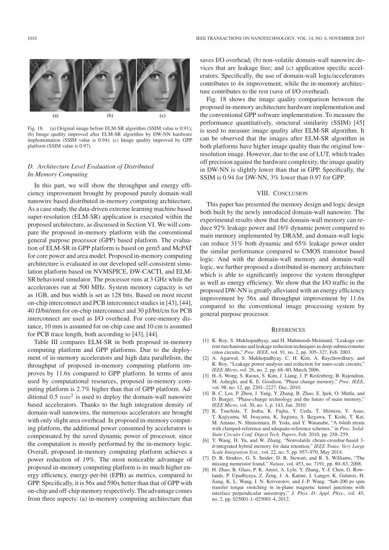
Fig. 18. (a) Original image before ELM-SR algorithm (SSIM value is 0.91);(b) Image quality improved after ELM-SR algorithm by DW-NN hardwareimplementation (SSIM value is 0.94); (c) Image quality improved by GPPplatform (SSIM value is 0.97).
D. Architecture Level Evaluation of DistributedIn-Memory Computing
In this part, we will show the throughput and energy effi-ciency improvement brought by proposed purely domain-wallnanowire based distributed in-memory computing architecture.As a case study, the data-driven extreme learning machine basedsuper-resolution (ELM-SR) application is executed within theproposed architecture, as discussed in Section VI. We will com-pare the proposed in-memory platform with the conventionalgeneral purpose processor (GPP) based platform. The evalua-tion of ELM-SR in GPP platform is based on gem5 and McPATfor core power and area model. Proposed in-memory computingarchitecture is evaluated in our developed self-consistent simu-lation platform based on NVMSPICE, DW-CACTI, and ELM-SR behavioral simulator. The processor runs at 3 GHz while theaccelerators run at 500 MHz. System memory capacity is setas 1GB, and bus width is set as 128 bits. Based on most recenton-chip interconnect and PCB interconnect studies in [43], [44],40 fJ/bit/mm for on-chip interconnect and 30 pJ/bit/cm for PCBinterconnect are used as I/O overhead. For core-memory dis-tance, 10 mm is assumed for on-chip case and 10 cm is assumedfor PCB trace length, both according to [43], [44].
Table III compares ELM-SR in both proposed in-memorycomputing platform and GPP platforms. Due to the deploy-ment of in-memory accelerators and high data parallelism, thethroughput of proposed in-memory computing platform im-proves by 11.6x compared to GPP platform. In terms of areaused by computational resources, proposed in-memory com-puting platform is 2.7% higher than that of GPP platform. Ad-ditional 0.5 mm2 is used to deploy the domain-wall nanowirebased accelerators. Thanks to the high integration density ofdomain-wall nanowires, the numerous accelerators are broughtwith only slight area overhead. In proposed in-memory comput-ing platform, the additional power consumed by accelerators iscompensated by the saved dynamic power of processor, sincethe computation is mostly performed by the in-memory logic.Overall, proposed in-memory computing platform achieves apower reduction of 19%. The most noticeable advantage ofproposed in-memory computing platform is its much higher en-ergy efficiency, energy-per-bit (EPB) as metrics, compared toGPP. Specifically, it is 56x and 590x better than that of GPP withon-chip and off-chip memory respectively. The advantage comesfrom three aspects: (a) in-memory computing architecture that
saves I/O overhead; (b) non-volatile domain-wall nanowire de-vices that are leakage free; and (c) application specific accel-erators. Specifically, the use of domain-wall logic/acceleratorscontributes to 4x improvement, while the in-memory architec-ture contributes to the rest (save of I/O overhead).
Fig. 18 shows the image quality comparison between theproposed in-memory architecture hardware implementation andthe conventional GPP software implementation. To measure theperformance quantitatively, structural similarity (SSIM) [45]is used to measure image quality after ELM-SR algorithm. Itcan be observed that the images after ELM-SR algorithm inboth platforms have higher image quality than the original low-resolution image. However, due to the use of LUT, which tradesoff precision against the hardware complexity, the image qualityin DW-NN is slightly lower than that in GPP. Specifically, theSSIM is 0.94 for DW-NN, 3% lower than 0.97 for GPP.
VIII. CONCLUSION
This paper has presented the memory design and logic designboth built by the newly introduced domain-wall nanowire. Theexperimental results show that the domain-wall memory can re-duce 92% leakage power and 16% dynamic power compared tomain memory implemented by DRAM; and domain-wall logiccan reduce 31% both dynamic and 65% leakage power underthe similar performance compared to CMOS transistor basedlogic. And with the domain-wall memory and domain-walllogic, we further proposed a distributed in-memory architecturewhich is able to significantly improve the system throughputas well as energy efficiency. We show that the I/O traffic in theproposed DW-NN is greatly alleviated with an energy efficiencyimprovement by 56x and throughput improvement by 11.6xcompared to the conventional image processing system bygeneral purpose processor.
REFERENCES
[1] K. Roy, S. Mukhopadhyay, and H. Mahmoodi-Meimand, “Leakage cur-rent mechanisms and leakage reduction techniques in deep-submicrometercmos circuits,” Proc. IEEE, vol. 91, no. 2, pp. 305–327, Feb. 2003.
[2] A. Agarwal, S. Mukhopadhyay, C. H. Kim, A. Raychowdhury, andK. Roy, “Leakage power analysis and reduction for nano-scale circuits,”IEEE Micro, vol. 26, no. 2, pp. 68–80, March 2006.
[3] H.-S. Wong, S. Raoux, S. Kim, J. Liang, J. P. Reifenberg, B. Rajendran,M. Asheghi, and K. E. Goodson, “Phase change memory,” Proc. IEEE,vol. 98, no. 12, pp. 2201–2227, Dec. 2010.
[4] B. C. Lee, P. Zhou, J. Yang, Y. Zhang, B. Zhao, E. Ipek, O. Mutlu, andD. Burger, “Phase-change technology and the future of main memory,”IEEE Micro, vol. 30, no. 1, p. 143, Jan. 2010.
[5] K. Tsuchida, T. Inaba, K. Fujita, Y. Ueda, T. Shimizu, Y. Asao,T. Kajiyama, M. Iwayama, K. Sugiura, S. Ikegawa, T. Kishi, T. Kai,M. Amano, N. Shimomura, H. Yoda, and Y. Watanabe, “A 64mb mramwith clamped-reference and adequate-reference schemes,” in Proc. Solid-State Circuits Conf. Digest Tech. Papers, Feb. 2010, pp. 258–259.
[6] Y. Wang, H. Yu, and W. Zhang, “Nonvolatile cbram-crossbar-based 3-d-integrated hybrid memory for data retention,” IEEE Trans. Very LargeScale Integration Syst., vol. 22, no. 5, pp. 957–970, May 2014.
[7] D. B. Strukov, G. S. Snider, D. R. Stewart, and R. S. Williams, “Themissing memristor found,” Nature, vol. 453, no. 7191, pp. 80–83, 2008.
[8] H. Zhao, B. Glass, P. K. Amiri, A. Lyle, Y. Zhang, Y.-J. Chen, G. Row-lands, P. Upadhyaya, Z. Zeng, J. A. Katine, J. Langer, K. Galatsis, H.Jiang, K. L. Wang, I. N. Krivorotov, and J.-P. Wang, “Sub-200 ps spintransfer torque switching in in-plane magnetic tunnel junctions withinterface perpendicular anisotropy,” J. Phys. D: Appl. Phys., vol. 45,no. 2, pp. 025001-1–025001-4, 2012.

WANG et al.: ENERGY-EFFICIENT NONVOLATILE IN-MEMORY COMPUTING ARCHITECTURE FOR EXTREME LEARNING MACHINE 1011
[9] G. E. Rowlands, T. Rahman, J. A. Katine, J. Langer, A. Lyle, H. Zhao, J.G. Alzate, A. A. Kovalev, Y. Tserkovnyak, Z. M. Zeng, H. W. Jiang, K.Galatsis, Y. M. Huai, P. K. Amiri, K. L. Wang, I. N. Krivorotov, and J.-P.Wang, “Deep subnanosecond spin torque switching in magnetic tunneljunctions with combined in-plane and perpendicular polarizers,” Appl.Phys. Lett., vol. 98, no. 10, pp. 102509-1–102509-3, 2011.
[10] H. Zhao, A. Lyle, Y. Zhang, P. K. Amiri, G. Rowlands, Z. Zeng, J. Katine,H. Jiang, K. Galatsis, K. L. Wang, I. N. Krivorotov, and J.-P. Wang, “Lowwriting energy and sub nanosecond spin torque transfer switching of in-plane magnetic tunnel junction for spin torque transfer random accessmemory,” J. Appl. Phys., vol. 109, no. 7, pp. 07C720-1–07C720-3, 2011.
[11] S. S. P. Parkin, M. Hayashi, and L. Thomas, “Magnetic domain-wallracetrack memory,” Science, vol. 320, no. 5873, pp. 190–194, 2008.
[12] L. Thomas, S.-H. Yang, K.-S. Ryu, B. Hughes, C. Rettner, D.-S. Wang,C.-H. Tsai, K.-H. Shen, and S. S. Parkin, “Racetrack memory: A high-performance, low-cost, non-volatile memory based on magnetic domainwalls,” in Proc. Electron. Devices Meeting, 2011, pp. 24–2.
[13] R. Venkatesan, V. Kozhikkottu, C. Augustine, A. Raychowdhury, K. Roy,and A. Raghunathan, “Tapecache: A high density, energy efficient cachebased on domain wall memory,” in Proc. IEEE Int. Symp. Low PowerElectron. Design, 2012, pp. 185–190.
[14] S. Matsunaga, J. Hayakawa, S. Ikeda, K. Miura, T. Endoh, H. Ohno, andT. Hanyu, “Mtj-based nonvolatile logic-in-memory circuit, futureprospects and issues,” in Proc. Conf. Design, Autom. Test Europe, 2009,pp. 433–435.
[15] S. Matsunaga, J. Hayakawa, S. Ikeda, K. Miura, H. Hasegawa, T. Endoh,H. Ohno, and T. Hanyu, “Fabrication of a nonvolatile full adder basedon logic-in-memory architecture using magnetic tunnel junctions,” Appl.Phys. Exp., vol. 1, no. 9, pp. 091301-1–091301-3, 2008.
[16] W. H. Kautz, “Cellular logic-in-memory arrays,” IEEE Trans. Comput.,vol. 100, no. 8, pp. 719–727, Aug. 1969.
[17] H. Kimura, T. Hanyu, M. Kameyama, Y. Fujimori, T. Nakamura, andH. Takasu, “Complementary ferroelectric-capacitor logic for low-powerlogic-in-memory vlsi,” IEEE J. Solid-State Circuits, vol. 39, no. 6,pp. 919–926, Jun. 2004.
[18] S. Paul, S. Mukhopadhyay, and S. Bhunia, “A circuit and architecturecodesign approach for a hybrid cmos–sttram nonvolatile fpga,” IEEETrans. Nanotechnol., vol. 10, no. 3, pp. 385–394, May 2011.
[19] T. Hanyu, K. Teranishi, and M. Kameyama, “Multiple-valued logic-in-memory vlsi based on a floating-gate-mos pass-transistor network,” inProc. Solid-State Circuits Conf.,1998, pp. 194–195.
[20] Y. Wang, H. Yu, D. Sylvester, and P. Kong, “Energy efficient in-memoryaes encryption based on nonvolatile domain-wall nanowire,” in Proc. De-sign, Autom. Test Eur. Conf. Exhib., 2014, pp. 1–4.
[21] M. D. Stiles and J. Miltat, “Spin-transfer torque and dynamics,” in SpinDynamics in Confined Magnetic Structures III. New York, NY, USA:Springer, 2006, pp. 225–308.
[22] D. Chiba, G. Yamada, T. Koyama, K. Ueda, H. Tanigawa, S. Fukami,T. Suzuki, N. Ohshima, N. Ishiwata, Y. Nakatani, and T. Ono, “Control ofmultiple magnetic domain walls by current in a co/ni nano-wire,” Appl.Phys. Exp., vol. 3, no. 7, pp. 073004-1–073004-3, 2010.
[23] W. Fei, H. Yu, W. Zhang, and K. S. Yeo, “Design exploration of hybridcmos and memristor circuit by new modified nodal analysis,” IEEE Trans.Very Large Scale Integration Syst., vol. 20, no. 6, pp. 1012–1025, Jun.2012.
[24] H. Yu and Y. Wang, “Nonvolatile state identification and nvm spice,” inDesign Exploration of Emerging Nano-Scale Non-Volatile Memory. NewYork, NY, USA: Springer, 2014, pp. 45–83.
[25] C. W. Smullen, V. Mohan, A. Nigam, S. Gurumurthi, and M. R. Stan,“Relaxing non-volatility for fast and energy-efficient stt-ram caches,” inProc. High Performance Comput. Archit., 2011, pp. 50–61.
[26] S. J. Wilton and N. P. Jouppi, “Cacti: An integrated cache and memoryaccess time, cycle time, area, leakage, and dynamic power model,” IEEEJ. Solid-State Circuits, vol. 31, no. 5, pp. 677–688, 1996.
[27] A. Iyengar and S. Ghosh, “Modeling and analysis of domain wall dynamicsfor robust and low-power embedded memory,” in Proc. Design Autom.Conf., 2014, pp. 1–6.
[28] H.-P. Trinh, W. Zhao, J.-O. Klein, Y. Zhang, D. Ravelsona, andC. Chappert, “Domain wall motion based magnetic adder,” Electron. Lett.,vol. 48, no. 17, pp. 1049–1051, 2012.
[29] L. An and B. Bhanu, “Image super-resolution by extreme learning ma-chine,” in Proc. Image Process., 2012, pp. 2209–2212.
[30] T. S. Furey, N. Cristianini, N. Duffy, D. W. Bednarski, M. Schummer,and D. Haussler, “Support vector machine classification and validation ofcancer tissue samples using microarray expression data,” Bioinformatics,vol. 16, no. 10, pp. 906–914, 2000.
[31] J. A. Suykens and J. Vandewalle, “Least squares support vector machineclassifiers,” Neural Process. Lett., vol. 9, no. 3, pp. 293–300, 1999.
[32] B. Yegnanarayana, Artificial Neural Networks. New Delhi, India: PHILearning Pvt. Ltd., 2004.
[33] M. T. Hagan, H. B. Demuth, M. H. Beale, and O. De Jesus, Neural NetworkDesign. Boston, MA, USA: PWS, 1996.
[34] G.-B. Huang, Q.-Y. Zhu, and C.-K. Siew, “Extreme learning machine:Theory and applications,” Neurocomputing, vol. 70, no. 1, pp. 489–501,2006.
[35] G.-B. Huang, Q.-Y. Zhu, and C.-K. Siew, “Extreme learning machine: anew learning scheme of feedforward neural networks,” in Proc. NeuralNetw., 2004, pp. 985–990.
[36] J. Dean and S. Ghemawat, “Mapreduce: Simplified data processing onlarge clusters,” ACM Commun., vol. 51, no. 1, pp. 107–113, 2008.
[37] (2012). Nvm-spice [Online]. Available: http://www.nvmspice.org/[38] Y. Wang, W. Fei, and H. Yu, “Spice simulator for hybrid cmos memris-
tor circuit and system,” in Proc. Cellular Nanoscale Netw. Appl., 2012,pp. 1–6.
[39] S. Li, J. H. Ahn, R. Strong, J. Brockman, D. Tullsen, and N. Jouppi,“Mcpat: An integrated power, area, and timing modeling framework formulticore and manycore architectures,” in Proc. IEEE Int. Symp. Microar-chit., 2009, pp. 469–480.
[40] N. Binkert, B. Beckmann, G. Black, S. K. Reinhardt, A. Saidi, A. Basu,J. Hestness, D. R. Hower, T. Krishna, S. Sardashti et al., “The gem5simulator,” ACM SIGARCH Computer Architecture News, vol. 39, no. 2,pp. 1–7, 2011.
[41] P. Padhan, P. LeClair, A. Gupta, K. Tsunekawa, and D. Djayaprawira,“Frequency-dependent magnetoresistance and magnetocapacitance prop-erties of magnetic tunnel junctions with mgo tunnel barrier,” Appl. Phys.Lett., vol. 90, no. 14, pp. 142105-1–142105-3, 2007.
[42] C. Ranger, R. Raghuraman, A. Penmetsa, G. Bradski, and C. Kozyrakis,“Evaluating mapreduce for multi-core and multiprocessor systems,” inProc. High Perform. Comput. Archit., 2007, pp. 13–24.
[43] S. Park, M. Qazi, L.-S. Peh, and A. P. Chandrakasan, “40.4 fj/bit/mmlow-swing on-chip signaling with self-resetting logic repeaters embeddedwithin a mesh noc in 45 nm soi cmos,” in Proc. Conf. Design, Autom. TestEurope, 2013, pp. 1637–1642.
[44] V. Kumar, R. Sharma, E. Uzunlar, L. Zheng, R. Bashirullah, P. Kohl,M. S. Bakir, and A. Naeemi, “Airgap interconnects: Modeling, opti-mization, and benchmarking for backplane, pcb, and interposer applica-tions,” IEEE Trans. Components, Packag. Manuf. Technol., vol. 4, no. 8,pp. 1335–1346, Aug. 2014.
[45] Z. Wang, A. C. Bovik, H. R. Sheikh, and E. P. Simoncelli, “Image qualityassessment: From error visibility to structural similarity,” IEEE Trans.Image Process., vol. 13, no. 4, pp. 600–612, Apr. 2004.
Yuhao Wang received the B.S. degree in microelec-tronics engineering from Xi’an Jiao Tong University,Xi’an, China, in 2011, and the Ph.D. degree in 2015from the School of Electrical and Electronic Engi-neering, Nanyang Technological University, Singa-pore. He is currently a Research Fellow at NanyangTechnological University. His research interests in-clude emerging nonvolatile memory, in-memory ar-chitecture and big-data analytics.
Hao Yu (M’06–SM’14) received the B.S. degreefrom Fudan University, Shanghai, China, in 1999, andthe M.S. and Ph.D. degrees from the Electrical En-gineering Department, University of California, LosAngeles, CA, USA, in 2007, with major in integratedcircuit and embedded computing. He was a SeniorResearch Staff at Berkeley Design Automation. SinceOctober 2009, he has been an Assistant Professor atthe School of Electrical and Electronic Engineering,Nanyang Technological University, Singapore. Hisprimary research interest is in emerging CMOS tech-
nologies such as 3DIC and RFIC designs at nanotera scale. He has 150 top-tierpeer-reviewed publications, four books and five book chapters. He received theBest Paper Award from the ACM Transactions on Design Automation of Elec-tronic Systems (TODAES) in 2010, Best Paper Award nominations in DAC06,ICCAD06, and ASP-DAC12, and Inventor Award from Semiconductor Re-search Cooperation. He is associate editor and technical program committeemember of several journals and conferences.

1012 IEEE TRANSACTIONS ON NANOTECHNOLOGY, VOL. 14, NO. 6, NOVEMBER 2015
Leibin Ni received the B.S. degree in microelectron-ics from Shanghai Jiao Tong University, Shanghai,China, in 2014. He is currently working toward theM.Eng. degree at the School of Electrical and Elec-tronic Engineering, Nanyang Technological Univer-sity, Singapore. His current research interests includeemerging nonvolatile memory platform and big-datain-memory computing.
Guang-Bin Huang (M’98–SM’04) received theB.Sc. degree in applied mathematics and the M.Eng.degree in computer engineering from NortheasternUniversity, Shenyang, China, in 1991 and 1994, re-spectively, and the Ph.D. degree in electrical engi-neering from Nanyang Technological University, Sin-gapore, in 1999. During undergraduate period, he alsoconcurrently studied at the Applied Mathematics De-partment and Wireless Communication Department,Northeastern University. From June 1998 to May2001, he worked as a Research Fellow at the Sin-
gapore Institute of Manufacturing Technology (formerly known as the GinticInstitute of Manufacturing Technology) where he has led/implemented severalkey industrial projects. From May 2001, he has been working as an AssistantProfessor and Associate Professor at the School of Electrical and ElectronicEngineering, Nanyang Technological University. His current research interestsinclude machine learning, computational intelligence, and extreme learning ma-chines. He serves as an Associate Editor of Neurocomputing and IEEE TRANS-ACTIONS ON SYSTEMS, MAN, AND CYBERNETICS: PART B.
Mei Yan, Chuliang Weng, Wei Yang, and Junfeng Zhao, biographies notavailable at the time of publication.