ieee transactions on nanotechnology, vol. 13, no. 1 ...yy582/papers/yong2014 - video-rate... ·...
TRANSCRIPT

IEEE TRANSACTIONS ON NANOTECHNOLOGY, VOL. 13, NO. 1, JANUARY 2014 85
Video-Rate Lissajous-Scan Atomic Force MicroscopyYuen Kuan Yong, Member, IEEE, Ali Bazaei, Member, IEEE, and S. O. Reza Moheimani, Fellow, IEEE
Abstract—Raster scanning is common in atomic force mi-croscopy (AFM). The nonsmooth raster waveform contains high-frequency content that can excite mechanical resonances of anAFM nanopositioner during a fast scan, causing severe distor-tions in the resulting image. The mainstream approach to avoidscan-induced vibrations in video-rate AFM is to employ a high-bandwidth nanopositioner with the first lateral resonance fre-quency above 20 kHz. In this paper, video-rate scanning on ananopositioner with 11.3-kHz resonance frequency is reported us-ing a smooth Lissajous scan pattern. The Lissajous trajectory isconstructed by tracking two sinusoidal waveforms on the lateralaxes of the nanopositioner. By combining an analog integral reso-nant controller (IRC) with an internal model controller, 1- and2-kHz single tone set-points were successfully tracked. High-quality time lapsed AFM images of a calibration grating recordedat 9 and 18 frames/s without noticeable image distortions are re-ported.
Index Terms—Atomic force microscopy, flexure-based, integralresonant control, internal model control, Lissajous-scan, non-raster scanning, video-rate.
I. INTRODUCTION
THE invention of scanning tunneling microscopy (STM) inearly 1980s facilitated imaging of conducting sample sur-
faces on atomic scale [1]. The need for imaging nonconductingsurfaces, at resolutions beyond the reach of optical microscopy,led to the invention of atomic force microscopy (AFM) later in1986 [2]. Since its debut, the AFM has become one of the mostversatile instruments for studying objects on the nanoscale. Ithas been used to interrogate, manipulate, and image a varietyof samples in vacuum, air, and liquid environments. The AFMhas brought about significant progress in a broad range of sci-entific disciplines and industries such as life sciences [3]–[5],semiconductor manufacturing [6], [7], nanometrology [8], [9],nanofabrication [10], [11] and high-density data storage sys-tems [12], [13].
Fig. 1 illustrates the main components of an AFM. The AFMis a mechanical microscope which uses an atomically sharp tiplocated at the end of a microcantilever to “feel” the surface of asample. The tip-sample interaction force causes the microcan-tilever to deflect and this deflection is measured by a laser and a
Manuscript received June 21, 2013; revised September 9, 2013; accepted Oc-tober 31, 2013. Date of publication November 25, 2013; date of current versionJanuary 6, 2014. This work was supported by Australian Research Council. Thereview of this paper was arranged by Associate Editor J. T. W. Yeow.
The authors are with the School of Electrical Engineering and ComputerScience, The University of Newcastle, Callaghan, NSW 2308, Australia (e-mail: [email protected]; [email protected]; [email protected]).
Color versions of one or more of the figures in this paper are available onlineat http://ieeexplore.ieee.org.
Digital Object Identifier 10.1109/TNANO.2013.2292610
Fig. 1. Basic components of AFM.
position sensitive photodiode (PSPD). A nanopositioner is usedto either move the tip or the sample in the x, y, and z directionsduring scanning.
Raster-based scanning has been the standard method of gen-erating images in various forms of scanning probe microscopy,including the STM [14], the scanning near-field optical mi-croscopy [15], scanning capacitance microscopy [16], and themagnetic force microscopy [17]. To construct a raster trajectory,one lateral axis of the nanopositioner is required to track a fasttriangular signal, while the other is set to track a slow ramp orstaircase signal. The spectrum of the triangle waveform not onlyconsists of its fundamental frequency, but also contains all ofits odd harmonics. The nanopositioner has a finite mechanicalbandwidth and a highly resonant nature. Tracking of the fast tri-angle waveform and its harmonics tends to excite the resonancefrequency of the nanopositioner [18], [19]. A typical solution toavoid exciting the resonant mode is to limit the fundamental fre-quency of the triangle waveform to the range 1/100th to 1/10th ofthe first lateral resonance frequency of the nanopositioner [20].This clearly impedes the scan rate of AFMs.
A common approach to avoid scan-induced vibrations dur-ing video-rate imaging is to use a high-bandwidth flexure-based nanopositioner, with the first lateral resonant peak above20 kHz [21], [22]. However, designing such a high-bandwidthnanopositioner could be a difficult task. It involves careful con-siderations of mechanical properties of flexures, as well aselectrical properties of piezoelectric stack actuators and drives,preloading of the piezoelectric stack actuators, and manufac-turing techniques [23]. In addition, the travel range of a po-sitioner is generally reduced as its resonance frequency is in-creased [23], [24]. Feedback control methods such as PPF [25],
1536-125X © 2013 IEEE. Personal use is permitted, but republication/redistribution requires IEEE permission.See http://www.ieee.org/publications standards/publications/rights/index.html for more information.

86 IEEE TRANSACTIONS ON NANOTECHNOLOGY, VOL. 13, NO. 1, JANUARY 2014
resonant control [26], integral resonant control (IRC) [27]–[30],and shunt damping [31], [32] have also been used to suppressresonance frequencies of nanopositioners, and hence, to mini-mize structural vibrations induced by the raster signal. Anotherapproach to avoid the excitation of structural resonant modes isinput-shaping [33], [34]. Feedforward control techniques [19],[24], [35] have also been implemented to improve the trackingperformance of nanopositioners during high-speed rastering.
Recently, nonraster scan methods such as spiral-scan [36],cycloid-scan [37], and Lissajous-scan methods [38], [39] havebeen proposed to significantly increase the scan speed of AFMs.All these nonraster scan methods involve tracking sinusoidalreferences on the lateral axes of the nanopositioner. Unlike thetriangular signals, sinusoids have narrow frequency spectrums.For a nanopositioner with a limited bandwidth, tracking of sinu-soidal references is a much easier task than tracking of triangularsignals. An example can be found in [38] where vibration-freeAFM images were obtained by tracking a 600-Hz Lissajous tra-jectory in closed-loop using a piezoelectric tube scanner with825-Hz resonance frequency. These scan results would be diffi-cult to achieve using the conventional raster-scan method.
This paper extends our previous work on high-speed AFMbased on tracking Lissajous patterns, reported in [38], tovideo-rate AFM using a high-speed nanopositioner with lateralresonance frequency of 11.3 kHz. An analog integral resonantcontroller (IRC) is designed and implemented to suppress thefirst dominant mode of each lateral axis of the nanopositioner.Internal model (IM) controllers are designed for the dampedsystem and implemented to track 1- and 2-kHz sinusoidalreferences. The inclusion of high harmonic components inthe IM controllers significantly improves the tracking errors.Compared to the previous video-rate AFM methods reportedin [40]–[42] that are based on conventional raster scanning,in open loop, and on higher bandwidth nanopositioners,the proposed video-rate Lissajous scan method uses noiseresilient IM controllers and a lower bandwidth nanopositioner.Compared to the low-speed Lissajous scan method presentedin [39], which uses linear H∞ controllers, the high-speedmethod proposed here uses IM control that can compensatefor the residual tracking errors due to piezoelectric actuatornonlinear effects such as hysteresis and creep.
The remainder of the paper continues as follows. A briefdescription of the Lissajous pattern is presented in Section II.Section III outlines the procedures involved in constructing avideo-rate Lissajous pattern for the AFM. Section IV discussesthe experimental setup. Design and implementation of the ana-log IRC and the IM controllers are discussed in Section V.This section also presents the noise analysis of the open- andclosed-loop systems. The open- and closed-loop AFM scans arepresented in Section VI. Section VII concludes the paper.
II. LISSAJOUS PATTERN
The Lissajous trajectory can be generated by driving the x-and y-axes of the nanopositioner with purely sinusoidal signalsthat contain slightly different frequencies, that is,
x (t) = Ax sin (2πfxt)
(a) (b)
(c) (d)
Fig. 2. Examples of Lissajous patterns with different fx /fy ratio.(a) fx /fy = 2. (b) fx /fy = 3/2. (c) fx /fy = 5/4. (d) fx /fy = 1.0476.
y (t) = Ay sin (2πfy t) . (1)
Here, Ax , Ay , fx , and fy are the amplitudes and frequencies ofthe sinusoids along the x- and y-axes, respectively. The shapeof the Lissajous pattern is dependent on the ratio fx/fy and thephase difference between the two sinusoids. For simplicity, weassume that the phase difference between the x- and y-signals iszero. However, a phase difference can be introduced to generatea variety of Lissajous patterns. Examples of the Lissajous pat-terns are shown in Fig. 2 for different fx/fy values. Note thatthe frequency difference between fx and fy also determines theperiod T in which the pattern evolves and repeats itself [38]. Tcan be calculated as T = 1/|fx − fy |.
In [38], we reported a detailed analytical framework for gen-erating a Lissajous pattern suitable for AFM. Four examplesof this pattern are plotted in Fig. 2(a)–(d). Readers are referredto [38] for a detailed analysis.
III. CONSTRUCTION OF LISSAJOUS TRAJECTORIES
FOR VIDEO-RATE AFM
To determine the parameters of the video-rate Lissajous tra-jectory, we follow the design steps proposed in [38]. These aresummarized below.Step 1: Select the scan size and resolution. A 3 μm×3 μm area
of a sample with a resolution of h = 30 nm is selected(h is the largest distance between two scan lines). Theintention is to generate an image that is comparable toa raster-scanned image with a resolution of 100 × 100pixels.
Step 2: Calculate N . The integer N is calculated by roundingthe following equation to the nearest integer:
N =πAxAy
h√
A2x + A2
y
(2)
where Ax = Ay = 1.5μm. N is calculated to be 111.
YONG et al.: VIDEO-RATE LISSAJOUS-SCAN ATOMIC FORCE MICROSCOPY 87
TABLE ILISSAJOUS PARAMETERS, FRAME RATES, AND SAMPLING FREQUENCIES
FOR A SCAN AREA OF 3 μM × 3 μM, AND A RESOLUTION OF h = 30 NM
Step 3: Determine the lateral scan frequencies fx and fy .fx
represents the scan frequency of the x-axis and must fitwithin the mechanical bandwidth of the nanopositioner;fy can be calculated from
fx
fy=
2N
2N − 1. (3)
Equation (3) ensures that the ratio fx/fy is a rationalnumber. This condition guarantees that the Lissajoustrajectory returns to its starting point and repeats itselfwith the same pattern after one period. We have chosento perform video-rate AFM at two scan speeds of fx =1and 2 kHz. From (3), the respective fy values are 995.49and 1990.99 Hz.
Step 4: Calculate the frame rate. The frame rate can be calcu-lated by fx/N . For fx = 1 kHz and fx = 2 kHz, theframe rates are 9 and 18 frames/s, respectively.
Step 5: Calculate the sampling frequency. The sampling fre-quency is required for data acquisition purposes duringAFM imaging. The sampling frequency fs can be ob-tained from
fs = 2 (2N − 1) fx. (4)
Table I summarizes the parameters of the two Lissajous trajec-tories, frame rates, and the corresponding sampling frequencies.
IV. EXPERIMENTAL SETUP
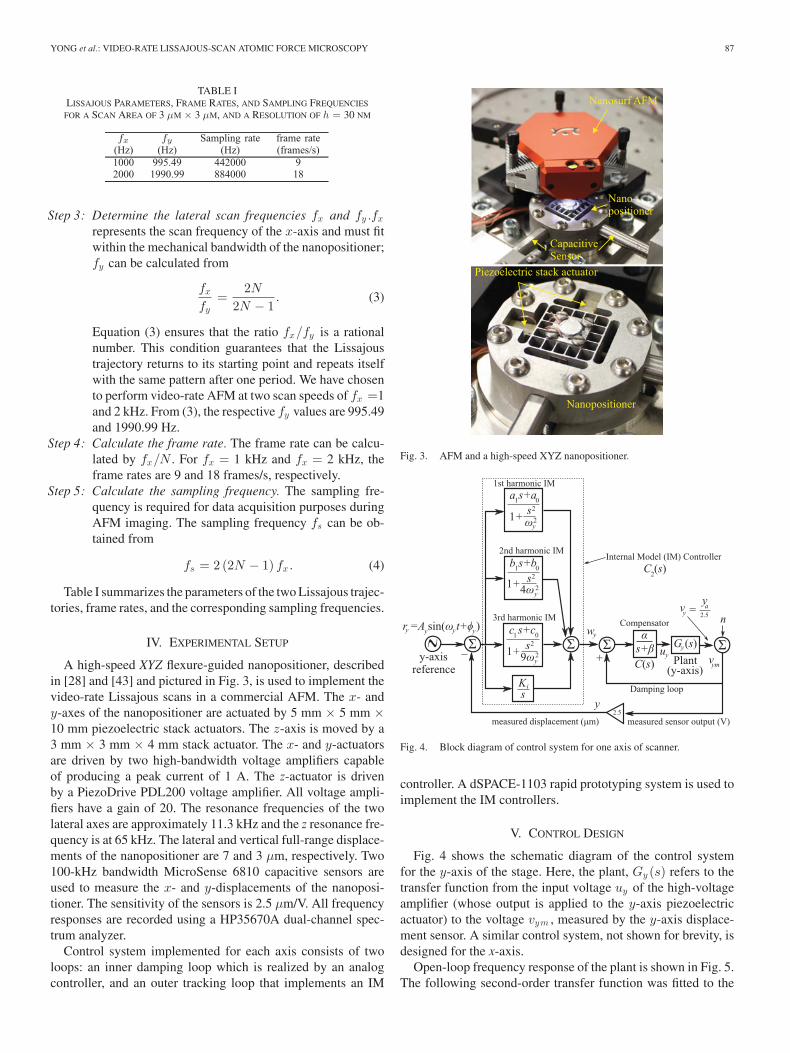
A high-speed XYZ flexure-guided nanopositioner, describedin [28] and [43] and pictured in Fig. 3, is used to implement thevideo-rate Lissajous scans in a commercial AFM. The x- andy-axes of the nanopositioner are actuated by 5 mm × 5 mm ×10 mm piezoelectric stack actuators. The z-axis is moved by a3 mm × 3 mm × 4 mm stack actuator. The x- and y-actuatorsare driven by two high-bandwidth voltage amplifiers capableof producing a peak current of 1 A. The z-actuator is drivenby a PiezoDrive PDL200 voltage amplifier. All voltage ampli-fiers have a gain of 20. The resonance frequencies of the twolateral axes are approximately 11.3 kHz and the z resonance fre-quency is at 65 kHz. The lateral and vertical full-range displace-ments of the nanopositioner are 7 and 3 μm, respectively. Two100-kHz bandwidth MicroSense 6810 capacitive sensors areused to measure the x- and y-displacements of the nanoposi-tioner. The sensitivity of the sensors is 2.5 μm/V. All frequencyresponses are recorded using a HP35670A dual-channel spec-trum analyzer.
Control system implemented for each axis consists of twoloops: an inner damping loop which is realized by an analogcontroller, and an outer tracking loop that implements an IM
Fig. 3. AFM and a high-speed XYZ nanopositioner.
Fig. 4. Block diagram of control system for one axis of scanner.
controller. A dSPACE-1103 rapid prototyping system is used toimplement the IM controllers.
V. CONTROL DESIGN
Fig. 4 shows the schematic diagram of the control systemfor the y-axis of the stage. Here, the plant, Gy (s) refers to thetransfer function from the input voltage uy of the high-voltageamplifier (whose output is applied to the y-axis piezoelectricactuator) to the voltage vym , measured by the y-axis displace-ment sensor. A similar control system, not shown for brevity, isdesigned for the x-axis.
Open-loop frequency response of the plant is shown in Fig. 5.The following second-order transfer function was fitted to the

88 IEEE TRANSACTIONS ON NANOTECHNOLOGY, VOL. 13, NO. 1, JANUARY 2014
TABLE IIPARAMETER VALUES OF THE CONTROL SYSTEMS
Fig. 5. Frequency responses of the open-loop plant, the compensator, and thedamping loop.
experimentally obtained data. Fig. 5 illustrates that this modelfits the measured data very closely
Gy (s) =0.01743s2 − 5300s + 9.168 × 10⁸
s2 + 8942s + 6.635 × 10⁹ . (5)
The control system for each axis consists of two feedbackloops; an inner loop and an outer loop. The inner loop consists ofa first-order IRC, denoted by C(s), that is designed to alleviatethe highly resonant dynamics of the stage. Parameter valuesof this compensator are reported in Table II. The associatedfrequency response is shown in Fig. 5.
The effectiveness of the damping controller can be observedfrom the experimentally obtained closed-loop frequency re-sponse of the inner loop (from the input wy to the sensor outputvym in Fig. 4), plotted in Fig. 5. The IRC reduces the resonancepeak from 19 to only 2 dB, which is a significant improvement.The associated stability margins are 10 dB and −128◦. Giventhe simple structure of the damping controller, the large band-width of the highly resonant plant and sampling rate limitationsof our real-time control system (dSPACE-DS1103), we decidedto implement the damping controller using the analog circuitshown in Fig. 6. The circuit has a negative dc gain which iscompensated by out of phase sensing and actuation configu-rations in the stage (not shown for brevity). The outer loop isdigitally implemented using dSPACE.
Fig. 6. Circuit diagram of the analog system used to implement the dampingloop. The minus sign at the output is for consistency with Fig. 4, where thenegative dc gain of the circuit is cancelled by the out-of-phase sensor/actuatorconfigurations of the stage, which is excluded from the plant model (5) forbrevity.
Due to the limited sampling rate of 80 kHz in dSPACE, thereexist small discontinuities in the discretized controller outputwy that cannot excite any vibrations as the inner loop is a well-damped continuous system. If both loops were implemented bydSPACE, such discontinuities would directly be applied to theplant input uy , exciting the resonant mode of the stage, lead-ing to undesirable vibrations. Fig. 5 also shows the simulatedfrequency response of the damping loop using the plant model(5) and the first order compensator model, where a good matchwith the experimental closed-loop data of the inner loop con-firms a valid implementation of the damping loop by the analogcircuit. The damping performance is also confirmed by the stepresponses shown in Fig. 7.
Having well-damped and hence better conditioned plants as-sociated with both x- and y-axes, we can incorporate IM con-trollers in the outer loops to achieve accurate tracking of thesinusoidal set-points as required in Lissajous scan AFM. Asshown in Fig. 4, the IM controller C2(s) contains an integratorand a second-order transfer function with imaginary poles thatmatch the fundamental frequency of the sinusoidal reference(first harmonic IM). We have also included second-order trans-fer functions that correspond to the second and third harmonicsof the reference in the controller. These additional controllerscan improve the steady-state tracking error resulting from plantnonlinearities such as hysteresis and creep, that manifest asharmonics of the reference frequency [38]. Note that due tothe nonlinearities, a pure single-tone sinusoidal actuation is notenough to generate the desired sine wave output. Assuming astatic nonlinearity, the ideal actuation waveform generating thedesired one-tone output (reference) through a nonlinear sys-tem is generally a periodic signal with the same period, whichhas infinite number of harmonics in addition to its fundamentalcomponent. If only one sinusoidal oscillator, at the fundamen-tal frequency, is implemented in the IM controller, it cannot

YONG et al.: VIDEO-RATE LISSAJOUS-SCAN ATOMIC FORCE MICROSCOPY 89
(a)
(b)
Fig. 7. Normalized step responses of the plant and the damping loop ob-tained by simulation and experiment. (a) Experimental step responses. (b) Stepresponses by simulation.
generate the higher harmonics required for the ideal actuation,resulting in a nonzero residual output error.
For the two reference frequencies of 1 and 2 kHz, the pa-rameter values of the IM controllers are recorded in Table IIand the associated stability margins are (6.8 dB, 52◦) and(10.8 dB, 57◦), respectively. Fig. 8 shows the experimentallyobtained and the simulated unit-step-responses of the controlsystems, demonstrating the modeling accuracy and acceptabletransient performances in a worst-case scenario.
We are now in a position to experimentally assess the perfor-mance of the control system in tracking 1- and 2-kHz sinusoidalreferences, required for video-rate Lissajous scans. We also in-vestigate the effectiveness of controlling higher order harmonicsin the IM controller. Both x- and y-axes of the scanner are si-multaneously driven, via their control systems, by sinusoidalreferences that slightly differ in frequency (by approximately0.45%). Each reference signal has an amplitude of 1.5 μm anda zero bias.
Fig. 9 shows the resulting steady-state tracking errors, withand without the third harmonic IM, for the 1-kHz control system.The root-mean-square (RMS) value of the positioning errors isalso indicated. It can be observed that incorporating the thirdharmonic IM in the controller significantly improves the track-ing performance. The experimentally obtained results for the2-kHz control system, shown in Fig. 10, also demonstrate simi-lar improvements, confirming the advantages of the high-orderharmonic elements in the IM controller. A nanometer-scale po-sitioning accuracy is achieved while tracking a 2-kHz sinusoidalreference that swings in the micrometer range, by proper con-trol of a nanopositioner whose resonance is at 11.3 kHz and is
(a)
(b)
Fig. 8. Unit step responses of the control systems obtained by simulation andexperiment. (a) Unit-step-response of closed-loop system with 1-kHz IM con-troller. (b) Unit-step-response of closed-loop system with 2-kHz IM controller.
(a)
(b)
Fig. 9. Experimental steady-state tracking errors of the 1-kHz control sys-tem for sinusoidal references with peak-to-peak amplitude of 3 μm, with andwithout the third harmonic IM component in controller C2 (s). (a) Steady-statetracking errors for 1-kHz control system for y-axis. (b) Steady-state trackingerrors for 1-kHz control system for x-axis.
subjected to uncertainties and nonlinearities such as hysteresis,creep, and cross coupling.

90 IEEE TRANSACTIONS ON NANOTECHNOLOGY, VOL. 13, NO. 1, JANUARY 2014
(a)
(b)
Fig. 10. Experimental steady-state tracking errors of the 2-kHz control sys-tem for sinusoidal references with peak-to-peak amplitude of 3 μm, with andwithout the third and the second harmonic IM components in controller C2 (s).(a) Steady-state tracking errors for 2-kHz control system of y-axis. (b) Steady-state tracking errors for 2-kHz control system of x-axis.
We are now in a position that we may assess the noise re-jection properties of the 1- and 2-kHz control systems. We firstmeasured the sensor noise output of the open-loop system (whenthe system was not actuated). Using the block diagram of thecontrol system in Fig. 4, the transfer function from the noisesource to the actual plant output ya := 2.5vy (projected noise)is
Tn (s) :=ya(s)n(s)
= −2.5Ln (s)
1 + Ln (s)(6)
where Ln = (2.5C2 − 1)CG, and factor of 2.5 μm/V convertsthe sensor output voltage to displacement. Applying no refer-ences, the actual plant output was calculated as the projectednoise using the aforementioned plant model. Fig. 11 shows theresults in time and frequency domains. Compared to 7.5 nm rmsvalue of the noise source, the rms values of the projected noisein 1- and 2-kHz control systems are 1.2 and 1.3 nm, respec-tively. Hence, the proposed controllers also reduce the effect ofsensor noise on the controlled position while maintaining highlyacceptable tracking performances.
VI. AFM RESULTS
This section evaluates the AFM imaging performance ofthe nanopositioner with the implementation of the proposedcontrol strategies discussed in Section V. The feedback con-trolled nanopositioner is mounted under a commercial NanosurfEasyScan 2 AFM, as shown in Fig. 3. Thus, the scanning stage ofthis commercial AFM is replaced with the high-speed nanopo-sitioner. An ASM 750-HD calibration grating is used to evaluate
Fig. 11. Measured noise source and the resulting projected noises in the controlsystems in time and frequency domains.
Fig. 12. Open-loop images obtained at 18 frames/s (fx =2 kHz). The imagewas severely distorted due to vibrations and poor tracking performance.
the video-rate images. The grating has a step height of 100 nmand a pitch of 738 nm. A National Instruments 4 MS/s PXI-6124data acquisition card is used to record the images.
AFMs can be operated in contact, semicontact, and dynamicmodes. Details of these scanning modes can be found in [44],[19] and [23]. AFM images presented here were obtained inconstant-height contact-mode. In this mode, the vertical feed-back loop is deactivated during scanning. The 3-D topographicimages of the sample were constructed by plotting the deflec-tion of the microcantilever versus the x- and y-positions of thesample.
Fig. 12 shows the open-loop image of a 3 μm × 3 μm sam-ple area obtained at 18 frames/s (fx =2 kHz). The image was

YONG et al.: VIDEO-RATE LISSAJOUS-SCAN ATOMIC FORCE MICROSCOPY 91
Fig. 13. Sequence of Lissajous images showing the process of fast zooming in of a sample area from 3 μm × 3 μm to 1 μm × 1 μm. Every third image in theseries is illustrated above. These series of images were captured at (a) 9 frames/s (fx =1 kHz) and (b) 18 frames/s (fx =2 kHz).
severely distorted due to vibrations and poor tracking perfor-mance of the nanopositioner in open loop.
Fig. 13 illustrates a sequence of closed-loop Lissajous imageswhich were obtained at 9 frames/s (fx =1 kHz) and 18 frames/s(fx =2 kHz). The images show a rapid zooming-in process ona sample area from 3 μm × 3 μm to 1 μm × 1 μm. Everythird image in the sequence is shown in the figure. With theproposed control strategies implemented, the image artifactsdue to vibrations and poor tracking were eliminated.
VII. CONCLUSION
In this paper, a nonraster scan method based on following aLissajous pattern was used to achieve video-rate atomic forcemicroscopy on a 11.3-kHz nanopositioner. An analog integralresonant controller was designed and implemented to suppressthe first resonant mode of each lateral axis of the nanoposi-tioner by 17 dB. IM controllers incorporating higher harmonic
components were used to significantly improve the tracking er-rors of the scanner. It was shown that the projected noise is muchsmaller than the sensor noise. This implies that the proposedcontrol strategies are capable of reducing the effect of sensornoise at the controlled position and simultaneously achievinghigh tracking performances. By combining the Lissajous-scanmethod with the proposed IRC and IM controllers, high-qualityAFM images were successfully recorded at 9 and 18 frames/s.
REFERENCES
[1] G. Binnig, H. Rohrer, C. Gerber, and E. Weibel, “Surface studies byscanning tunneling microscopy,” vol. 49, no. 1, pp. 57–61, 1982.
[2] G. Binnig, C. F. Quate, and C. Gerber, “Atomic force microscope,” vol.56, pp. 930–933, 1986.
[3] T. Ando, “High-speed atomic force microscopy coming of age,” Nan-otechnology, vol. 23, no. 6, p. 062001, 2012.
[4] T. Ando, T. Uchihashi, N. Kodera, D. Yamamoto, A. Miyagi, M. Taniguchi,and H. Yamashita, “High-speed AFM and nano-visualization ofbiomolecular processes,” Pflugers Archiv. Eur. J. Physiol., vol. 456, no. 1,pp. 211–225, 2008.

92 IEEE TRANSACTIONS ON NANOTECHNOLOGY, VOL. 13, NO. 1, JANUARY 2014
[5] P. Hinterdorfer and Y. F. Dufrene, “Detection and localization of singlemolecular recognition events using atomic force microscopy,” NatureMethods, vol. 3, pp. 347–355, 2006.
[6] K. Wiesauer and G. Springholz, “Fabrication of semiconductor nanos-tructures by nanoindentation of photoresist layers using atomic force mi-croscopy,” J. Appl. Phys., vol. 88, no. 12, pp. 7289–7297, 2000.
[7] R. A. Oliver, “Advances in AFM for the electrical characterization ofsemiconductors,” Rep. Progr. Phys., vol. 71, no. 7, p. 076501, 2008.
[8] Y. Hua, C. Coggins, and S. Park, “Advanced 3D metrology atomic forcemicroscope,” in Proc. IEEE/SEMI Adv. Semicond. Manuf. Conf., 2010,pp. 7–10.
[9] L. Tetard, A. Passian, R. H. Farahi, B. H. Davison, S. Jung,A. J. Ragauskas, A. L. Lereu, and T. Thundat, “Nanometrology of delig-nified Populus using mode synthesizing atomic force microscopy,” Nan-otechnology, vol. 22, no. 46, p. 465702, 2011.
[10] J. A. Vicary and M. J. Miles, “Real-time nanofabrication with high-speedatomic force microscopy,” Nanotechnology, vol. 20, no. 9, p. 095302,2009.
[11] S. Kim and S.-W. Kim, “AFM-based nanofabrication with assistance offemtosecond pulse laser radiation,” J. Phys.: Conf. Series, vol. 61, no. 1,pp. 550–554, 2007.
[12] G. Binnig, M. Despont, U. Drechsler, W. Haberle, M. Lutwyche,P. Vettiger, H. Mamin, B. Chui, and T. Kenny, “Ultrahigh-density atomicforce microscopy data storage with erase capability,” Appl. Phys. Lett.,vol. 74, no. 9, pp. 1329–1331, 1999.
[13] P. Vettiger, G. Cross, M. Despont, U. Drechsler, U. Durig, B. Gotsmann,W. Haberle, M. A. Lantz, H. E. Rothuizen, R. Stutz, and G. K. Binnig,“The ‘Milipede’—Nanotechnology entering data storage,” vol. 1, no. 1,pp. 39–55, 2002.
[14] G. Binnig and H. Rohrer, “The scanning tunneling microscope,” Scientif.Amer., vol. 253, pp. 50–56, 1986.
[15] D. W. Pohl, U. C. Fischer, and U. T. Drig, “Scanning near-field opti-cal microscopy (SNOM),” J. Microsc., vol. 152, no. 3, pp. 853–861,1988.
[16] C. C. Williams, W. P. Hough, and S. A. Rishton, “Scanning capacitancemicroscopy on a 25 nm scale,” Appl. Phys. Lett., vol. 55, no. 2, pp. 203–205, 1989.
[17] Y. Martin and H. K. Wickramasinghe, “Magnetic imaging by ‘force mi-croscopy’ with 1000 [A-ring] resolution,” Appl. Phys. Lett., vol. 50, no. 20,pp. 1455–1457, 1987.
[18] S. O. R. Moheimani, “Invited review article: Accurate and fast nanopo-sitioning with piezoelectric tube scanners: Emerging trends and futurechallenges,” Rev. Scientif. Instrum., vol. 79, no. 7, p. 071101, 2008.
[19] G. M. Clayton, S. Tien, K. K. Leang, Q. Zou, and S. Devasia, “A review offeedforward control approaches in nanopositioning for high-speed SPM,”J. Dyn. Syst., Meas., Control, vol. 131, no. 6, p. 061101, 2009.
[20] S. Devasia, E. Eleftheriou, and S. O. R. Moheimani, “A survey of controlissues in nanopositioning,” vol. 15, pp. 802–823, 2007.
[21] G. Schitter, K. J. Astrom, B. DeMartini, P. J. Thurner, K. L. Turner, andP. K. Hansma, “Design and modeling of a high-speed AFM-scanner,” vol.15, no. 5, pp. 906–915, 2007.
[22] B. J. Kenton and K. K. Leang, “Design and control of a three-axis serial-kinematic high-bandwidth nanopositioner,” IEEE/ASME Trans. Mecha-tronics, vol. 17, no. 2, pp. 356–368, 2012.
[23] Y. K. Yong, S. O. R. Moheimani, B. J. Kenton, and K. K. Leang, “In-vited review article: High-speed flexure-guided nanopositioning: Mechan-ical design and control issues,” Rev. Scientif. Instrum., vol. 83, no. 12,p. 121101, 2012.
[24] Y. K. Yong, S. Aphale, and S. O. R. Moheimani, “Design, identificationand control of a flexure-based XY stage for fast nanoscale positioning,”IEEE Trans. Nanotechnol., vol. 8, no. 1, pp. 46–54, Jan. 2009.
[25] B. Bhikkaji, M. Ratnam, A. J. Fleming, and S. O. R. Moheimani, “High-performance control of piezoelectric tube scanners,” vol. 15, no. 5, pp.853–866, 2007.
[26] A. Sebastian, A. Pantazi, S. O. R. Moheimani, H. Pozidis, andE. Eleftheriou, “Achieving sub-nanometer precision in a MEMS storagedevice during self-servo write process,” IEEE Trans. Nanotechnol., vol. 7,no. 5, pp. 586–595, Sep. 2008.
[27] S. S. Aphale, A. J. Fleming, and S. O. R. Moheimani, “Integral resonantcontrol of collocated smart structures,” Smart Mater. Struct., vol. 16,pp. 439–446, 2007.
[28] Y. K. Yong, B. Bhikkaji, and S. O. R. Moheimani, “Design, modeling andFPAA-based control of a high-speed atomic force microscope nanoposi-tioner,” IEEE/ASME Trans. Mechatronics, vol. 18, no. 3, pp. 1060–1071,Jun. 2013.
[29] A. J. Fleming, S. Aphale, and S. O. R. Moheimani, “A new method forrobust damping and tracking control of scanning probe microscope posi-tioning stages,” IEEE Trans. Nanotechnol., vol. 9, no. 4, pp. 438–448, Jul.2010.
[30] Y. K. Yong, A. Fleming, and S. O. R. Moheimani, “A novel piezoelectricstrain sensor for simultaneous damping and tracking control of a high-speed nanopositioner,” IEEE/ASME Trans. Mechatronics, vol. 18, no. 3,pp. 1113–1121, Jun. 2013.
[31] S. Aphale, A. J. Fleming, and S. O. R. Moheimani, “High speed nano-scale positioning using a piezoelectric tube actuator with active shuntcontrol,” Micro Nano Lett., vol. 2, no. 1, pp. 9–12, 2007.
[32] A. A. Eielsen and A. J. Fleming, “Passive shunt damping of a piezoelectricstack nanopositioner,” in Proc. Amer. Control Conf., 2010, pp. 4963–4968.
[33] G. Schitter, P. J. Thurner, and P. K. Hansma, “Design and input-shapingcontrol of a novel scanner for high-speed atomic force microscopy,”Mechatronics, vol. 18, pp. 282–288, 2008.
[34] A. J. Fleming and A. G. Wills, “Optimal periodic trajectories for band-limited systems,” IEEE Trans. Control. Syst. Technol., vol. 13, no. 3,pp. 552–562, May 2009.
[35] K. K. Leang and S. Devasia, “Feedback-linearized inverse feedforward forcreep, hysteresis, and vibration compensation in piezoactuators,” IEEEControl Syst. Technol.: Spec. Issue Dyn. Control Micro- Nano-Scale Syst.,vol. 15, no. 5, pp. 927–935, Sep. 2007.
[36] I. A. Mahmood, S. O. R. Moheimani, and B. Bhikkaji, “A new scanningmethod for fast atomic force microscopy,” IEEE Trans. Nanotechnol.,vol. 10, no. 2, pp. 203–216, Mar. 2011.
[37] Y. K. Yong, S. O. R. Moheimani, and I. R. Petersen, “High-speed cycloid-scan atomic force microscopy,” Nanotechnology, vol. 21, no. 36,p. 365503, 2010.
[38] A. Bazaei, Y. K. Yong, and S. O. R. Moheimani, “High-speed Lissajous-scan atomic force microscopy: Scan pattern planning and control designissues,” Rev. Scientif. Instrum., vol. 83, no. 6, p. 063701, 2012.
[39] T. Tuma, J. Lygeros, V. Kartik, A. Sebastian, and A. Pantazi, “High-speed multiresolution scanning probe microscopy based on Lissajous scantrajectories,” Nanotechnology, vol. 23, no. 18, p. 185501, 2012.
[40] A. D. L. Humphris, J. K. Hobbs, and M. J. Miles, “Ultrahigh-speed scan-ning near-field optical microscopy capable of over 100 frames per second,”Appl. Phys. Lett., vol. 83, pp. 6–8, 2003.
[41] A. D. L. Humphris, M. J. Miles, and J. K. Hobbs, “A mechanical micro-scope: High-speed atomic force microscopy,” Appl. Phys. Lett., vol. 86,p. 034106, 2005.
[42] T. Ando, T. Uchihashi, and T. Fukuma, “High-speed atomic force mi-croscopy for nano-visualization of dynamic biomolecular processes,”Progr. Surf. Sci., vol. 83, pp. 337–437, 2008.
[43] Y. K. Yong and S. O. R. Moheimani, “Design of an inertially coun-terbalanced Z-nanopositioner for high-speed atomic force microscopy,”IEEE/ASME Trans. Nanotechnol., vol. 12, no. 2, pp. 137–145, Mar. 2013.
[44] D. Abramovitch, S. Andersson, L. Pao, and G. Schitter, “A tutorial onthe mechanisms, dynamics, and control of atomic force microscopes,” inProc. Amer. Control Conf., Jul. 2007, pp. 3488–3502.
Yuen Kuan Yong (M’09) received the B.Eng. de-gree (first Class Hons.) in mechatronic engineeringand the Ph.D. degree in mechanical engineering fromThe University of Adelaide, Adelaide, Australia, in2001 and 2007, respectively.
She is currently an Australian Research CouncilDECRA Fellow with the School of Electrical En-gineering and Computer Science, The University ofNewcastle. Her research interests include the designand control of nanopositioning systems, high-speedatomic force microscopy, finite-element analysis of
smart materials and structures, and sensing and actuation.Dr. Yong was a recipient of the 2008 IEEE/ASME International Conference
on Advanced Intelligent Mechatronics (AIM) Best Conference Paper FinalistAward. She is a member of the Technical Program Committee of AIM and theInternational Conference on Manipulation, Manufacturing, and Measurementon the Nanoscale (3M-NANO). She is also an Associate Editor of the EditorialBoard of the International Journal of Advanced Robotic Systems.

YONG et al.: VIDEO-RATE LISSAJOUS-SCAN ATOMIC FORCE MICROSCOPY 93
Ali Bazaei (M’01) received the B.Sc. and M.Sc. de-grees from Shiraz University, Shiraz, Iran, and thePh.D. degrees from University of Western Ontario,London, ON, Canada, and Tarbiat Modares Univer-sity, Tehran, Iran, in 1992, 1995, 2004, and 2009,respectively, all in electrical engineering.
From September 1995 to January 2000, he wasan Instructor with Yazd University, Yazd, Iran. FromSeptember 2004 to December 2005, he was a Re-search Assistant with the Department of Electricaland Computer Engineering, University of Western
Ontario, London, ON, Canada. He is currently a research academic with theSchool of Electrical Engineering and Computer Science, The University ofNewcastle, Australia. His research interests include the general area of non-linear systems including control and modeling of structurally flexible systems,friction modeling and compensation, neural networks, and microposition sen-sors.
S. O. Reza Moheimani (M’07–F’01) received theB.Sc. degree in electrical and electronic engineeringfrom Shiraz University, Shiraz, Iran, in 1990 and theM.Eng.Sc. and Ph.D. degrees in electrical and elec-tronic engineering from the University of New SouthWales, Sydney, New South Wales, Australia, at theAustralian Defence Force Academy, Canberra, Aus-tralia, in 1993 and 1996, respectively.
He joined The University of Newcastle, Callaghan,Australia, in 1997, where he is a Professor of electri-cal engineering and an Australian Research Council
(ARC) Future Fellow. He is the Founder and the Director of the Laboratory forDynamics and Control of Nanosystems, a multimillion-dollar state-of-the-artresearch facility. During 2003–2010, he was the Associate Director of the ARCCentre of Excellence for Complex Dynamic Systems and Control. His currentresearch interests include area of ultrahigh-precision mechatronic systems, withparticular emphasis on dynamics and control at the nanometer scale, includingapplications of control and estimation in nanopositioning systems for high-speedscanning probe microscopy, modeling and control of microcantilever-based de-vices, control of microactuators in microelectromechanical systems, and controlissues related to ultrahigh-density probe-based data-storage systems.
Prof. Moheimani is a Fellow of the International Federation of AutomaticControl (IFAC) and the Institute of Physics (U.K.). He is a corecipient of the2007 IEEE TRANSACTIONS ON CONTROL SYSTEMS TECHNOLOGYOutstanding Paper Award and the 2009 IEEE Control Systems TechnologyAward, together with a group of researchers from IBM Zurich Research Labs,where he has held several visiting appointments. He has served on the editorialboards of a number of journals, including the IEEE/ASME TRANSACTIONSON MECHATRONICS, IEEE TRANSACTIONS ON CONTROL SYSTEMSTECHNOLOGY, and Control Engineering Practice. He has chaired several in-ternational conferences and workshops and currently chairs the IFAC TechnicalCommittee on Mechatronic Systems.