624 ieee transactions on nanotechnology, vol. 14, no. …
TRANSCRIPT
624 IEEE TRANSACTIONS ON NANOTECHNOLOGY, VOL. 14, NO. 4, JULY 2015
Nanostructured Thermionics for Conversion of Lightto Electricity: Simultaneous Extraction
of Device ParametersAmir H. Khoshaman, Andrew T. Koch, Mike Chang, Harrison D. E. Fan,
Mehran Vahdani Moghaddam, and Alireza Nojeh
Abstract—Thermionic conversion involves the direct conversionof heat, including light-induced heat, from a heat source, e.g., so-lar energy, to electricity. Although the concept is almost a hundredyears old, the progress of thermionic convertors has been limited byissues such as the space-charge effect and availability of materialswith desirable mechanical and electrical properties, while main-taining a low work function. Nanotechnology could help addresssome of the main challenges that thermionic convertors face. How-ever, existing models, which were developed for macroscopic con-vertors, are not capable of describing all aspects of nanostructureddevices. We present a method to evaluate the output characteristicsof thermionic convertors with a higher precision than the existingmodels and the ability to simulate a broader range of parame-ters, including temperatures, active surface areas, interelectrodedistances, and work functions. These features are crucial for thecharacterization of emergent devices due to the unknowns involvedin their internal parameters; the model’s high numerical precisionand flexibility allows one to solve the reverse problem and to eval-uate the internal parameters of the device from a set of simpleexperimental data. As an experimental case, a carbon nanotubeforest was used as the emitter and locally heated to thermionicemission temperatures using a 50-mW-focused laser beam. Thecurrent–voltage characteristics were measured and used to solvethe reverse problem to obtain the internal parameters of the device,which were shown to be consistent with the values obtained usingother methods.
Index Terms—Carbon nanotubes, light induced thermionicemission, thermionic emission, thermionic conversion, Vlaslov’sequation.
I. INTRODUCTION
PHOTOVOLTAIC devices use optical generation of chargecarriers. Thermionic energy convertors (TECs), on the
other hand, employ heat, which could also be generated bylight, and act as a heat engine without moving parts to generateelectricity by means of thermionic emission.
Manuscript received November 5, 2014; accepted April 21, 2015. Date ofpublication April 24, 2015; date of current version July 7, 2015. This workwas supported by the Natural Sciences and Engineering Research Council, theCanada Foundation for Innovation, the British Columbia Knowledge Develop-ment Fund, the BCFRST Foundation, the British Columbia Innovation Council,the University of British Columbia, and the Peter Wall Institute for AdvancedStudies.
The authors are with the Department of Electrical and Computer Engineering,University of British Columbia, Vancouver, BC V6T 1Z4, Canada (e-mail:[email protected]; [email protected]; [email protected]; [email protected]; [email protected]; [email protected]).
Color versions of one or more of the figures in this paper are available onlineat http://ieeexplore.ieee.org.
Digital Object Identifier 10.1109/TNANO.2015.2426149
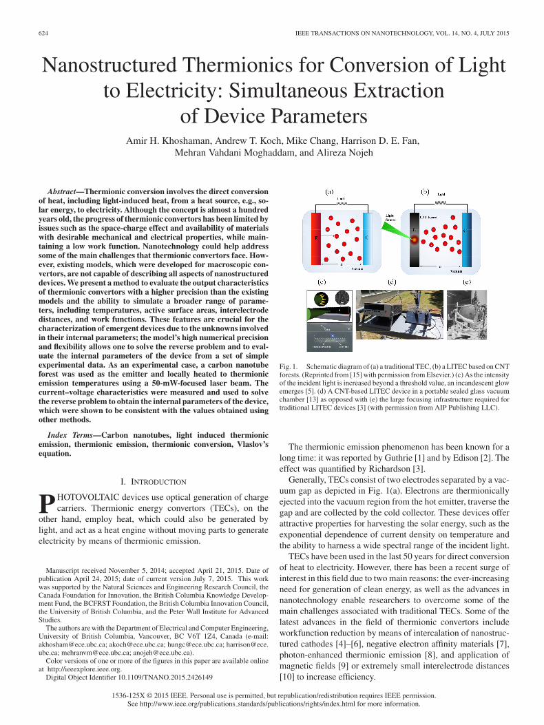
Fig. 1. Schematic diagram of (a) a traditional TEC, (b) a LITEC based on CNTforests. (Reprinted from [15] with permission from Elsevier.) (c) As the intensityof the incident light is increased beyond a threshold value, an incandescent glowemerges [5]. (d) A CNT-based LITEC device in a portable sealed glass vacuumchamber [13] as opposed with (e) the large focusing infrastructure required fortraditional LITEC devices [3] (with permission from AIP Publishing LLC).
The thermionic emission phenomenon has been known for along time: it was reported by Guthrie [1] and by Edison [2]. Theeffect was quantified by Richardson [3].
Generally, TECs consist of two electrodes separated by a vac-uum gap as depicted in Fig. 1(a). Electrons are thermionicallyejected into the vacuum region from the hot emitter, traverse thegap and are collected by the cold collector. These devices offerattractive properties for harvesting the solar energy, such as theexponential dependence of current density on temperature andthe ability to harness a wide spectral range of the incident light.
TECs have been used in the last 50 years for direct conversionof heat to electricity. However, there has been a recent surge ofinterest in this field due to two main reasons: the ever-increasingneed for generation of clean energy, as well as the advances innanotechnology enable researchers to overcome some of themain challenges associated with traditional TECs. Some of thelatest advances in the field of thermionic convertors includeworkfunction reduction by means of intercalation of nanostruc-tured cathodes [4]–[6], negative electron affinity materials [7],photon-enhanced thermionic emission [8], and application ofmagnetic fields [9] or extremely small interelectrode distances[10] to increase efficiency.
1536-125X © 2015 IEEE. Personal use is permitted, but republication/redistribution requires IEEE permission.See http://www.ieee.org/publications standards/publications/rights/index.html for more information.

KHOSHAMAN et al.: NANOSTRUCTURED THERMIONICS FOR CONVERSION OF LIGHT TO ELECTRICITY 625
An overview of the new prospects for thermionic conversionoffered by nanotechnology is given in Ref. [11].
Due to their high-temperature and mechanical stability, car-bon nanotubes (CNTs) are viable candidates for thermionicemission [12] and energy conversion applications [13]. Due tothermal dissipation in bulk conductors, light induced thermionicemission (LITE) requires very high optical powers, obtainablefor example, by using a large and complex apparatus to focusand collect sunlight as shown in Fig. 1(e) [14]. In particular,the heating situation can be drastically different in nanotube-based cathodes compared to bulk conductors. Our group haspreviously reported light-induced localized heating in multi-wall carbon nanotubes (MWCNT) forests [15]. This “Heat Trapeffect” enables localized heating to temperatures above 2000 Kusing a low-power beam of visible light, leading to localizedthermionic electron emission as depicted in Fig. 1(b)–(c). Basedon this effect, our group has subsequently demonstrated a vac-uum thermionic convertor (see Fig. 1(d)), [13].
Upon light-induced heating of the emitter, the electrons inthe high-energy Fermi tail have enough energy to overcomethe workfunction barrier. These electrons are ejected fromthe surface of the emitter and traverse the inter-electrodedistance to finally reach the cold collector. The difference be-tween the electrochemical potential energies of the two elec-trodes is transformed into work in the external load throughwhich the electrons travel back to the emitter.
Hatsopoulos and Gyftopoulos proposed a method to coupleVlaslov’s and Poisson’s equations in the space-charge limitedregime, assuming the electrons in the interelectrode space actas a collisionless gas with a Boltzmann velocity distribution[16]–[17]. This method can be used to evaluate the current–voltage (I–V) characteristics in the space-charge limited modeof thermionic convertors. However, this strategy has never beenused to solve the reverse problem and to obtain the internalparameters of the device from the I–V curves. This is becauseconventional thermionic devices are made using metal elec-trodes with known properties, such as workfunction, and theentire electrode is typically heated; parameters such as emis-sion spot area are well known and temperature can be easilymeasured. Therefore, Hatsopoulos and Gyftopoulos assumed auniform temperature profile in their model [16], [17]. However,as will be shown in this paper, a large temperature gradient mayexist in nanomaterial-based thermionics. For instance, in a CNT-based light induced thermionic energy convertor (LITEC), onlya small portion (with a radius, r, on the order of several hundredmicrometers) of the nanotube array may be heated. The exactvalue of the workfunction depends on the local properties andtemperature of the illuminated spot [18]. Moreover, the presenceof adsorbates can have noticeable effects on the workfunction ofCNTs. For instance, the adsorption of water molecules will re-duce the workfunction [19]–[20] while the presence of organicmolecules on the CNT tip will result in larger workfunctions[18]. Additionally, the local density of states at the tip andsidewalls of CNTs are different, leading to different values ofworkfunctions [21].
Therefore, the study of these emerging thermionic devicesrequires a strategy to characterize their internal parameters. In
addition, the lack of sufficient computational power and a stablealgorithm have made it difficult to tackle the more computa-tionally intensive, reverse problem in the past. The integralsinvolved in this method do not have exact analytical solutionsand behave non-linearly as the internal parameters of the de-vice are varied. In fact, the numerical approximations tabulatedin Ref. [16] are sufficient to predict the space-charge limitedbehaviour of thermionic convertors only in a limited range oftemperatures, workfunctions, and interelectrode spacings.
II. THEORY AND MODEL
It is assumed that electrons are thermionically emitted fromthe cathode as governed by the Richardson–Dushman equation,Jsat = AT 2
E exp(−φE /kB TE ), where Jsat denotes the satura-tion current density, i.e., the maximum current density attain-able from the emitter at the emitter’s temperature, TE · kB is theBoltzmann constant, and A = 1.202 × 10⁶A · m−2 · K−2 is theRichardson–Dushman constant [22].
The electrons reaching the other electrode (collector or anode)are completely collected and run through the external circuit.The methodology in this section follows the earlier descrip-tion of operation of TECs in the space-charge limited regime[6], [17]. It is described here how the numerical accuracy andthe range of applicability can be further enhanced using a newalgorithm. Moreover, the I–V characteristics of the TEC areobtained for different regimes of device operation. The high nu-merical accuracy, applicability to a wide range of parameters,and modelling of the entire I–V characteristics, in addition toa stable algorithm, make solving the more challenging reverseproblem possible. The general method to solve the direct prob-lem is to couple Poisson’s and Vlaslov’s equations. Vlaslov’sequation applies when electrons in the interelectrode region areapproximated as a collisionless ideal gas [23]. In the simplestone-dimensional (1-D) case, i.e., when a uniform electric fieldis applied only in the direction normal to the emitter and col-lector’s surface (e.g., along the x-axis), an analytical solution ispossible. The solution includes functions and integrals that canbe solved numerically. The operation of the TECs in the space-charge mode is discussed in Ref. [17]. We provide a summaryof the key points along with important equations for the sakeof clarity. We also propose an algorithm that can be utilized toincrease the accuracy of the method proposed in Ref. [16] tocalculate the I–V characteristics.
A TEC can operate in two or three distinct regimes (or modes),depending on the electric potential difference between the elec-trodes (see Fig. 2). The width of each mode and the onset of thesubsequent mode depend on the internal parameters of the TECsuch as temperature, interelectrode gap distance, and the work-functions. Fig. 2(a) shows the I–V characteristics of a typicalTEC in its various operating regimes. The appropriate motivediagrams that are the analogs of the band-diagrams in solidstate physics are also included. The emitter and collector areassumed to have the same Richardson–Dushman constant andmaintained at TE and TC , respectively. The motive diagram ofa TEC operating under negative and positive biases is depictedin Fig. 2(b) and (c).
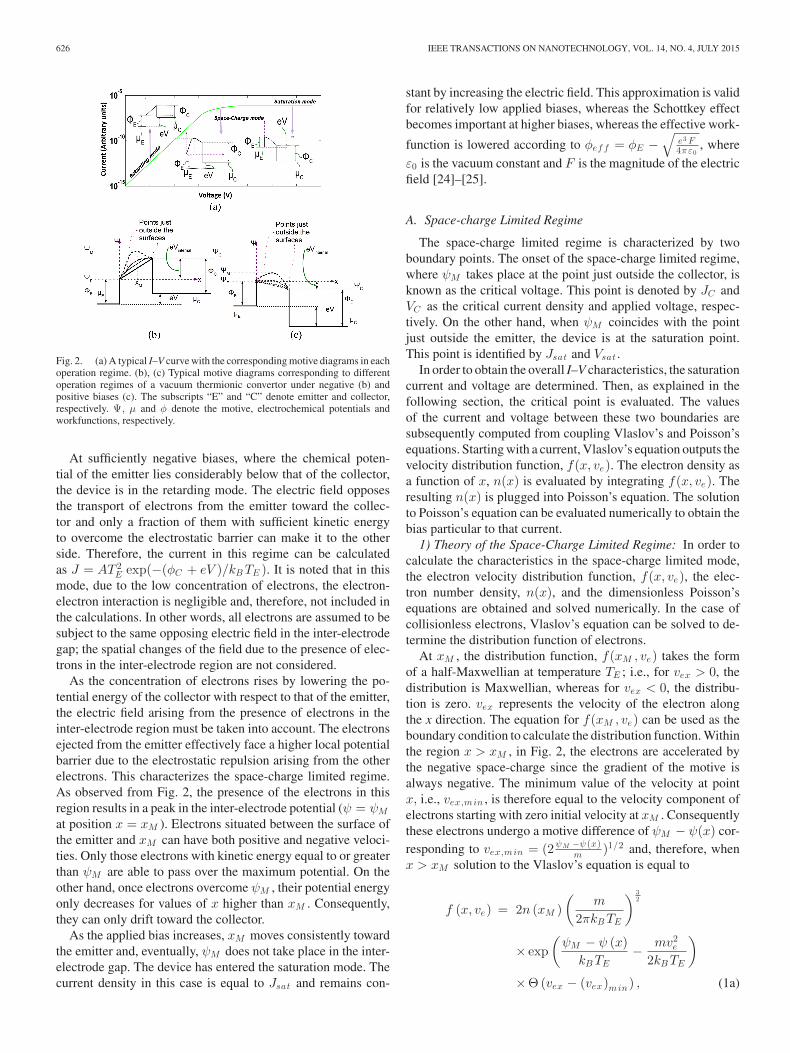
626 IEEE TRANSACTIONS ON NANOTECHNOLOGY, VOL. 14, NO. 4, JULY 2015
Fig. 2. (a) A typical I–V curve with the corresponding motive diagrams in eachoperation regime. (b), (c) Typical motive diagrams corresponding to differentoperation regimes of a vacuum thermionic convertor under negative (b) andpositive biases (c). The subscripts “E” and “C” denote emitter and collector,respectively. Ψ, μ and φ denote the motive, electrochemical potentials andworkfunctions, respectively.
At sufficiently negative biases, where the chemical poten-tial of the emitter lies considerably below that of the collector,the device is in the retarding mode. The electric field opposesthe transport of electrons from the emitter toward the collec-tor and only a fraction of them with sufficient kinetic energyto overcome the electrostatic barrier can make it to the otherside. Therefore, the current in this regime can be calculatedas J = AT 2
E exp(−(φC + eV )/kB TE ). It is noted that in thismode, due to the low concentration of electrons, the electron-electron interaction is negligible and, therefore, not included inthe calculations. In other words, all electrons are assumed to besubject to the same opposing electric field in the inter-electrodegap; the spatial changes of the field due to the presence of elec-trons in the inter-electrode region are not considered.
As the concentration of electrons rises by lowering the po-tential energy of the collector with respect to that of the emitter,the electric field arising from the presence of electrons in theinter-electrode region must be taken into account. The electronsejected from the emitter effectively face a higher local potentialbarrier due to the electrostatic repulsion arising from the otherelectrons. This characterizes the space-charge limited regime.As observed from Fig. 2, the presence of the electrons in thisregion results in a peak in the inter-electrode potential (ψ = ψM
at position x = xM ). Electrons situated between the surface ofthe emitter and xM can have both positive and negative veloci-ties. Only those electrons with kinetic energy equal to or greaterthan ψM are able to pass over the maximum potential. On theother hand, once electrons overcome ψM , their potential energyonly decreases for values of x higher than xM . Consequently,they can only drift toward the collector.
As the applied bias increases, xM moves consistently towardthe emitter and, eventually, ψM does not take place in the inter-electrode gap. The device has entered the saturation mode. Thecurrent density in this case is equal to Jsat and remains con-
stant by increasing the electric field. This approximation is validfor relatively low applied biases, whereas the Schottkey effectbecomes important at higher biases, whereas the effective work-
function is lowered according to φef f = φE −√
e3 F4πε0
, where
ε0 is the vacuum constant and F is the magnitude of the electricfield [24]–[25].
A. Space-charge Limited Regime
The space-charge limited regime is characterized by twoboundary points. The onset of the space-charge limited regime,where ψM takes place at the point just outside the collector, isknown as the critical voltage. This point is denoted by JC andVC as the critical current density and applied voltage, respec-tively. On the other hand, when ψM coincides with the pointjust outside the emitter, the device is at the saturation point.This point is identified by Jsat and Vsat .
In order to obtain the overall I–V characteristics, the saturationcurrent and voltage are determined. Then, as explained in thefollowing section, the critical point is evaluated. The valuesof the current and voltage between these two boundaries aresubsequently computed from coupling Vlaslov’s and Poisson’sequations. Starting with a current, Vlaslov’s equation outputs thevelocity distribution function, f(x, ve). The electron density asa function of x, n(x) is evaluated by integrating f(x, ve). Theresulting n(x) is plugged into Poisson’s equation. The solutionto Poisson’s equation can be evaluated numerically to obtain thebias particular to that current.
1) Theory of the Space-Charge Limited Regime: In order tocalculate the characteristics in the space-charge limited mode,the electron velocity distribution function, f(x, ve), the elec-tron number density, n(x), and the dimensionless Poisson’sequations are obtained and solved numerically. In the case ofcollisionless electrons, Vlaslov’s equation can be solved to de-termine the distribution function of electrons.
At xM , the distribution function, f(xM , ve) takes the formof a half-Maxwellian at temperature TE ; i.e., for vex > 0, thedistribution is Maxwellian, whereas for vex < 0, the distribu-tion is zero. vex represents the velocity of the electron alongthe x direction. The equation for f(xM , ve) can be used as theboundary condition to calculate the distribution function. Withinthe region x > xM , in Fig. 2, the electrons are accelerated bythe negative space-charge since the gradient of the motive isalways negative. The minimum value of the velocity at pointx, i.e., vex,min , is therefore equal to the velocity component ofelectrons starting with zero initial velocity at xM . Consequentlythese electrons undergo a motive difference of ψM − ψ(x) cor-responding to vex,min = (2ψM −ψ (x)
m )1/2 and, therefore, whenx > xM solution to the Vlaslov’s equation is equal to
f (x, ve) = 2n (xM )(
m
2πkB TE
) 32
× exp(
ψM − ψ (x)kB TE
− mv2e
2kB TE
)
×Θ (vex − (vex)min ) , (1a)
KHOSHAMAN et al.: NANOSTRUCTURED THERMIONICS FOR CONVERSION OF LIGHT TO ELECTRICITY 627
where m is the mass of the electron, ve = (v2ex + v2
ey + v2ez )
1/2
is the electron speed, and Θ is the Heaviside step function.On the other hand, at x < xM , the electrons are decelerated by
the electric field and can have both positive and negative veloc-ities along the x direction. This leads to a negative minimumvelocity along the x direction, vex,min = −(2ψM −ψ (x)
m )1/2 .Therefore, when x ≤ xM , the velocity distribution function isgiven by
f (x, ve) = 2n (xM )(
m
2πkB TE
) 32
× exp(
ψM − ψ (x)kB TE
− mv2e
2kB TE
)
×Θ (vex + (vex)min ) . (1b)
Based on this explanation, electrons on either side of xM
also take on a half-Maxwellian velocity distribution with thepeak shifted from 0 to vx,min . The next step is to calculate theelectron number density, n(x), by integration of the velocitydistribution function over the entire velocity space at x. Thisresults in
n (x) = n (xM ) exp (γ)
{1 − erf
(γ1/2
),
1 + erf(γ1/2
),
x > xM
x ≤ xM
(2)where γ ≡ (ψM − ψ(x))/kB TE is the dimensionless potentialand erf is the error function.
In order to obtain the dimensionless Poisson’s equation, x isdivided by the Debye length given by LD ≡ ( ε0 kB TE
2e2 ne (xM ) )12 [23].
The resulting equation is
d2γ
dζ2 =12
exp (γ) ×{
1 − erf(γ1/2
),
1 + erf(γ1/2
),
ζ ≥ 0
ζ < 0(3)
where ζ ≡ (x − xM )/LD is the dimensionless distance. Notingthat ψM is a stationary point of ψ(x), the corresponding bound-ary conditions are obtained as γ(ζ=0) = 0 and ( dγ
dζ )(ζ=0) = 0.Double-integrating the equation and utilizing the boundary con-ditions lead to
ζ = −∫ γ
0
dα[exp (α) + exp (α) erf
(α
12
)− 2
(απ
) 12 − 1
]1/2
(4a)for ζ < 0 and
ζ =∫ γ
0
dα[exp (α) − exp (α) erf
(α
12
)+ 2
(απ
) 12 − 1
]1/2
(4b)for ζ > 0.
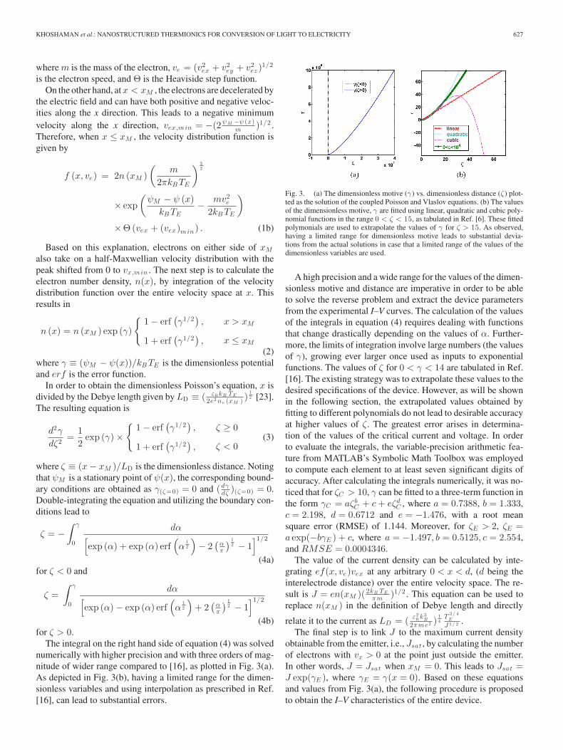
The integral on the right hand side of equation (4) was solvednumerically with higher precision and with three orders of mag-nitude of wider range compared to [16], as plotted in Fig. 3(a).As depicted in Fig. 3(b), having a limited range for the dimen-sionless variables and using interpolation as prescribed in Ref.[16], can lead to substantial errors.
Fig. 3. (a) The dimensionless motive (γ) vs. dimensionless distance (ζ) plot-ted as the solution of the coupled Poisson and Vlaslov equations. (b) The valuesof the dimensionless motive, γ are fitted using linear, quadratic and cubic poly-nomial functions in the range 0 < ζ < 15, as tabulated in Ref. [6]. These fittedpolymonials are used to extrapolate the values of γ for ζ > 15. As observed,having a limited range for dimensionless motive leads to substantial devia-tions from the actual solutions in case that a limited range of the values of thedimensionless variables are used.
A high precision and a wide range for the values of the dimen-sionless motive and distance are imperative in order to be ableto solve the reverse problem and extract the device parametersfrom the experimental I–V curves. The calculation of the valuesof the integrals in equation (4) requires dealing with functionsthat change drastically depending on the values of α. Further-more, the limits of integration involve large numbers (the valuesof γ), growing ever larger once used as inputs to exponentialfunctions. The values of ζ for 0 < γ < 14 are tabulated in Ref.[16]. The existing strategy was to extrapolate these values to thedesired specifications of the device. However, as will be shownin the following section, the extrapolated values obtained byfitting to different polynomials do not lead to desirable accuracyat higher values of ζ. The greatest error arises in determina-tion of the values of the critical current and voltage. In orderto evaluate the integrals, the variable-precision arithmetic fea-ture from MATLAB’s Symbolic Math Toolbox was employedto compute each element to at least seven significant digits ofaccuracy. After calculating the integrals numerically, it was no-ticed that for ζC > 10, γ can be fitted to a three-term function inthe form γC = aζb
C + c + eζdC , where a = 0.7388, b = 1.333,
c = 2.198, d = 0.6712 and e = −1.476, with a root meansquare error (RMSE) of 1.144. Moreover, for ζE > 2, ζE =a exp(−bγE ) + c, where a = −1.497, b = 0.5125, c = 2.554,and RMSE = 0.0004346.
The value of the current density can be calculated by inte-grating ef(x, ve)vex at any arbitrary 0 < x < d, (d being theinterelectrode distance) over the entire velocity space. The re-sult is J = en(xM )( 2kB TE
πm )1/2 . This equation can be used toreplace n(xM ) in the definition of Debye length and directly
relate it to the current as LD = ( ε20 k 3
B
2πme2 )14
T3 / 4E
J 1 / 2 .The final step is to link J to the maximum current density
obtainable from the emitter, i.e., Jsat , by calculating the numberof electrons with vx > 0 at the point just outside the emitter.In other words, J = Jsat when xM = 0. This leads to Jsat =J exp(γE ), where γE = γ(x = 0). Based on these equationsand values from Fig. 3(a), the following procedure is proposedto obtain the I–V characteristics of the entire device.

628 IEEE TRANSACTIONS ON NANOTECHNOLOGY, VOL. 14, NO. 4, JULY 2015
Fig. 4. Comparison of the estimated value of the critical point voltage, VC ,when calculated using the assumptions made by Hatsopoulos, VC ,H a t , and theactual value of VC obtained from iteratively solving the problem at different (a)interelectrode distances and (b) emitter temperatures. These results are calcu-lated for typical values of device parameters of φE = 4.6 eV, φC = 4.0 eV.The radius of the hot spot, r, is assumed to be 100 μm. In part (a), TE = 2000 Kand in part (b), d = 700 μm.
2) Current-Voltage Characteristics at the Critical and Sat-uration Points: At the saturation point, the maximum mo-tive takes place at the point just outside the emitter (xM = 0and J = JS ). Therefore, ζE = 0 and ζ(x = d) = ζC = d−0
LD=
(2πme2
ε20 k 3
B)
14
J1 / 2E s d
T3 / 4E
, where d is the interelectrode distance. Based
on this value of ζC , γC is interpolated from Fig. 3(a). Followingthe notations in Fig. 2, with the origin of the x coordinate atthe point just outside the emitter, the saturation voltage, Vsat iscalculated as (φE − φC − γC kTE ). In calculating the criticalpoint characteristics, it is noted that at this point, the maximummotive occurs just outside the collector (xM = d). Therefore,
γE = ln(Jsat/JC ), |ζE | =(
0 − d
LD
)=
(2πme2
ε20k
3B
) 14 J
1/2C d
T3/4E
and ζC = 0. In order to compute JC , Hatsopoulus made theassumption that at this point, the distance |ζE | reaches itsmaximum value (2.554 from Fig. 3(a)). Therefore, JC canbe calculated from this value of |ζE | and then replaced intothe Richardson–Dushman equation to evaluate the critical pointvoltage, VC . This estimation, as presented in Fig. 4(a) and (b),leads to numerical errors. The value of the VC calculated usingthe assumption |ζE | = 2.554 is denoted by VC,H at . These val-ues are compared with the VC values that are obtained using thefollowing proposed method. According to Fig. 4, the approxi-mation made can lead to considerable error in determining thevalue of VC .
We propose this method to calculate the exact value of VC asfollows:
a. As a first approximation, JC and VC are calculated fol-lowing the method explained above.
b. Values of γE = ln (J/Jsat) are computed for 10−6 <J
JC< 103 .
c. ζE is computed for each γE , based on their relation fromFig. 3(a).
d. ζC is calculated from ζC = d−xM
x0= d
xo− ζE . If ζC < 0,
the maximum motive occurs outside the interelectrode gapand, therefore, the device does not enter the space-chargeregime, and operates in the retarding mode. The smallestcurrent that sets ζC = 0, is equal to the actual value of JC .
Fig. 5. The entire I–V characteristics and the important boundary points (crit-ical and saturation voltages and currents) were calculated for a wide range ofdevice parameters. The effects of altering (a) the interelectrode gap size and (b)the hot spot temperature on the I–V characteristics are included in here. Thevalues of the currents and voltages at the boundary points (critical and saturationpoints, represented by subscripts “C” and “sat”, respectively), are tabulated inhere.
e. VC is calculated from the Richardson–Dushmanequation in the retarding regime: J = AT 2
E exp(−(φC + eV )/kTE ).
The value of 10−6 for the ratio of currents allows for calcula-tions of actual critical point currents up to 6 orders of magnitudedifferent from the estimated value. If the integrals are not cal-culated for a wider range, it will not be possible to calculate theexact value of JC , as large values of γE are required in Step c.
3) Output Current-Voltage Characteristics in the Space-Charge Limited Regime: In order to calculate the I–V char-acteristics, the following algorithm is proposed:
a. A procedure similar to the Steps b–d in calculating thecritical point is employed, except that the current is chosenwithin the range of JC < J < Jsat .
b. The values of γC are computed from the relation betweenγC and ζC , as illustrated in Fig. 3(a).
c. The output voltage is calculated from Fig. 2 as(φE − φC ) + kB TE (γE − γC ).
Fig. 5(a) and (b) demonstrate the effects of changing the gapwidth and the emitter’s temperature on the I–V characteristics ofthe device, respectively. In the retarding and saturation regimes,the current is determined using the Richardson–Dushman equa-tion with the proper value of the energy barrier that the electronencounters when travelling from the emitter to the collector. Onthe other hand, in the space-charge limited regime, numericalsolutions of equation (2) are used to calculate the characteris-tics. The entire I–V characteristics are eventually obtained bycombining the I–V curves within these three regions.
B. Non-Uniform Temperature Profile at the Emitter
So far, we have assumed that the temperature is uniformacross the illuminated area. This can be a reasonable assumptionin the case of the bulk TEC device with large dimensions.However, a detailed analysis of the new generation of TECswith much smaller dimension reveals the presence of tempera-ture gradients. For instance, in a real LITEC device, inspection

KHOSHAMAN et al.: NANOSTRUCTURED THERMIONICS FOR CONVERSION OF LIGHT TO ELECTRICITY 629
Fig. 6. (a) Temperature profile on the hot spot of the CNT-based LIETC. (b)Contributions of different temperature contour rings to the total current acrossa hot spot with a radius r = 200 μm.
of the temperature profile reveals an average temperaturegradient of several degrees of kelvin over a micrometer at atypical input laser power of 50 mW [26]. Therefore, a uniformtemperature profile is not realistic and the influence of theexistence of different areas with various temperatures has tobe included in the model. In order to model this effect, thecircular heat-spot area is divided into different rings withdifferent temperatures (T (rn )), with rn being the distanceof the nth ring from the center of the beam. Each ring isconsidered as a thermionic convertor contributing to the overallcurrent. Linear and Gaussian temperature profiles were used toinvestigate this effect. In the case of a linear temperature profile,T (rn ) = (T0 − Tmax) r
r0+ Tmax , this leads to an average tem-
perature of Taver = 1πr 2
0∫ r00 T (rn )2πrdr = 1
3 (2T0 + Tmax),where Tmax is the maximum temperature, T0 = T (r0),and r0 is the radius of the thermionic emission area (seeFig. 6(a)). The value of T0 is chosen such that the contributionfrom the ring at T = T0 , is less than 10−4 % to the overallcurrent. In the case of a Gaussian temperature distribution,T (r) = Tmax exp( r 2
αr 20), where α = ln(T0/Tmax), leads to
Taver = Tmaxα(−1 + exp(1/α)). The contributions of differ-ent temperatures when the thermionic emission area is dividedinto 10 rings are represented in Fig. 6(b). As observed, theaverage spatial temperature of the spot (2020 K) does not fullyrepresent the thermionic emission behavior of the spot. Thereason is the exponential dependence of the emission currenton the temperature of the emitter. Therefore, the definingtemperature of the device is closer to the maximum temperaturethan the spatial average temperature. Remarkably, one singletemperature cannot fully represent the system in any case. Atnegative biases, higher-temperature elements with less areacontribute predominantly to the current (2710 K with an area of5.59 × 103 μm2). On the other hand, near the saturation regime,the higher-surface-area rings with relatively lower temperaturesdominate. The reason is the high- and low-temperature areasfacing the same energy barrier at sufficiently negative biases(φC + e|V |). However, in the space-charge limited regime,higher-temperature sectors feel a larger barrier due to the in-creased space-charge, since they have a higher current density.
III. EXPERIMENTAL RESULTS AND COMPARISONS
A. Experimental Set-Up
Millimeter-long MWCNT forests were grown in a home-built chemical vapor deposition reaction chamber over a highly
Fig. 7. (a) The schematic of the experimental set-up for I–V measurementsof a CNT-based LITEC. (b) The incandescent spot on the side-wall of theCNT forest as imaged by a CCD camera. (c) The internal parameters of theLIETC device are obtained by solving the reverse problem and fitting to theexperimental results as depicted in the legend of the plot.
p-doped silicon wafer coated with successive layers of 10 nm ofAlumina and 1 nm of Iron. Some of the catalysts were patternedto form cubically shaped forests with a base width of 1 mmseparated by a distance of ∼500 μm. This pattern facilitated thecharacterization of the illuminated spot on the sidewalls of theCNT forests. CNTs were grown on the catalyst by following arecipe similar to the one used in [13].
The following experimental set-up (see Fig. 7(a)) was adoptedfor the experiments. The chips containing CNT forests weremounted on a sample holder and placed in a high-vacuum cham-ber (10−5–10−6 torr). The vacuum chamber was equipped withPirani and cold cathode gauges that allowed the pressure to bemonitored within a wide range (103–10−3 and 10−2–10−10 torr,respectively). A precision leak valve was used to control thepressure inside the chamber. The CNT sample was used as thecathode and was illuminated on its sidewall through the anode.An indium thin oxide glass slide with 84 % transparency or an85 % transparent stainless steel mesh were used as the anode.The gap width was set to less than 1 mm. The cathode wassurrounded by an open-ended aluminum cube, kept at the samepotential as the anode.
The laser was focused on the sidewalls of the CNT forest bymeans of a lens with a 15-cm focal length. Two manual highprecision microactuators were used to move laterally along thewidth of the forest, allowing one to determine the location ofthe illuminated spot for characterization purposes. The lens wasplaced approximately 15 cm away from the anode through aviewport and its exact position was controlled by a high pre-cision motorized microactuator (with a precision of 200 nm)controlled by a computer. Several different types of lasers, in-cluding three lasers from Laserglow Technologies (Electra Pro-40 (405 nm), Scorpius-500 (1064 nm) and Hercules (532 nm))and a 300-mW, 532-nm Green DPSS Laser from Alltech so-lutions were used. Two optical attenuators and a power reader
630 IEEE TRANSACTIONS ON NANOTECHNOLOGY, VOL. 14, NO. 4, JULY 2015
were used to adjust the power to the desired value. A chargedcoupled device (CCD) camera was used to measure the area ofthe laser spot on the forest (see Fig. 7(b)). The I–V character-istics were measured by sweeping from negative (retarding) topositive (collection) voltages using Keithley 6430 and 6517aelectrometers. Since the voltage is swept over a wide rangein our experiments, the magnitude of current varies dramati-cally each time (typically from less than 1 pA to ∼10 μA fora voltage sweep in the range of −4–10 V at TE = 2300 K).At positive biases higher than the saturation voltage of theLITEC device (typically V = 30 V to ensure that the saturationregime is properly covered), the current is on the order of tensof μAs.
B. Extracting the Experimental Parameters
As explained in the theoretical section, each regime of oper-ation follows a certain set of equations. Each internal parameterof the LITEC device affects the I–V characteristics in a uniqueway. For instance, increasing the gap width (from Fig. 5) in-creases the width of the space-charge region while maintainingthe same level of saturation current. Raising the emitter’s tem-perature shifts the entire I–V curve upwards (increasing currentat an exponential rate), while maintaining the intersection of thetwo tangent lines to the characteristics in the retarding and thesaturation modes at a fixed voltage point, Vm = (φC − φE )/e.Changing φE affects the saturation point voltage and currentwhile altering the thermionic emission area’s radius (r) shiftsthe entire curve upward or downward. To distinguish betweenthe alterations caused by TE or r, it is noted that the former hasa more palpable effect in negative biases, while the latter shiftsthe curve uniformly. Although it seems that each set of param-eters will lead to only a unique I–V profile, solving for each ofthe parameters is a challenging problem. In order to solve thisreverse problem, a graphical user interface was developed tocalculate the I–V characteristics based on the proposed proce-dure, allowing one to select different temperature profiles. Eachof the internal parameters are adjusted while their impact on theI–V profile is studied in real time. In order to test the uniqueness,a set of reasonable values of internal parameters were chosen inrandom, the I–V curves were generated based on the proposedprocedure in the previous section, and the results were used tosolve the reverse problem. When the temperature was assumedto be uniform, the reverse problem resulted in unique estima-tions of the internal parameters, with ±0.1 eV of accuracy forworkfunctions,∼± 50 K for TE and∼± 20 μm for the spot-sizeradius. The estimation of the inter-electrode distance dependson how deep the device is within the space-charge region. Atrelatively low d values, where VC is close to Vsat , the length ofthe space-charge region is negligible and, therefore, the impactof the gap width on the I–V profile will not be noticeable. Con-sequently, only an upper bound for d can be determined in suchcases.
Fig. 7(c) shows the experimental I–V characteristics fromillumination of the sample (with a stainless steel mesh as theanode) by 40 mW of a 405-nm laser fitted to simulation curvesidentified by a fixed-gradient temperature profile.
The effective hot spot radius (121 μm) is comparable withthe image taken by a CCD camera (∼150 μm). The estimatedtemperature (2 150 K) when assuming a linear temperature dis-tribution along the hot spot matches closely with the results thatour group previously obtained from fitting the incandescencespectra to black body radiation [15], and the estimated work-function of CNTs (4.7 eV) is consistent with the values obtainedby other methods [27].
Since the modelling presented in this paper is based on a1-D potential profile with infinitely large electrodes, it requiressome justification to use this model to extract the parameters ofa CNT-based LITEC. In the Appendix section, we show that our1-D model can effectively capture the experimental conditionsby a relatively small error.
Simultaneous measurement of all of these parameters that per-tain to a certain experiment in LITEC has not been possible in thepast. For instance, in order to measure the workfunction, a com-mon method such as ultraviolet spectroscopy can be employed.However, considering that the exact workfunction depends onthe local morphology of the CNTs and the temperature [28], itwould be extremely challenging, if not impossible, to have theilluminated spot on the CNTs with exactly the same amount ofintensity as that used in the thermionic conversion experiment.Besides the difficulty in determining the actual workfunction,the temperature may vary widely depending on the local den-sity of the CNT forest. For instance, the Richardson–Dushmanconstants calculated from the thermionic emission data from[19] were in discrepancy with values obtained for metals. Thisissue was attributed to the extra surface roughness and differentsurface area for CNTs compared to metals. Furthermore, mea-surement of the hot-spot area depends on the resolution as wellas the bandwidth of the CCD camera used for the measurements.Therefore, the area measured by a CCD camera might be differ-ent from the effective area contributing to thermionic emission.However, using I–V curves and following the proposed strategyprovides a consistent method for determination of the effectivearea of the hot spot. Moreover, the effective gap width betweenthe electrodes, though being on the same order as its equivalentphysical value, can be different due to the collection efficiencyof the electrons. The collection efficiency depends on the con-figuration of the electrodes and the geometry of the structure.As a result, the value of the gap width obtained from fitting tosimulation curves can be interpreted as the effective gap width.The magnitude of this parameter is proportional to the physicalinterelectrode distance divided by the collection coefficient.
IV. SUMMARY
A method was proposed based on the simultaneous solu-tions of Vlaslov and Poisson equations to calculate the out-put characteristics of thermionic convertors. The numericalaccuracy and the range of applicability of the method weresubstantially enhanced by applying robust algorithms. It wasdemonstrated that this method can be employed to solve the re-verse problem and calculate the internal parameters, e.g. work-functions, interelectrode distances, effective areas and tem-peratures of thermionic convertors. It was shown that the
KHOSHAMAN et al.: NANOSTRUCTURED THERMIONICS FOR CONVERSION OF LIGHT TO ELECTRICITY 631
emergent nanomaterial-based thermionic convertors, though op-erating on the same overall principles, have some distinct fea-tures such as spatially varying workfunctions and the presenceof temperature gradients, which require more sophisticated sim-ulation methods to study them. Due to the high stability of theproposed method, a versatile range of parameters can be solvedfor and, therefore, the method can address the numerical diffi-culties associated with new thermionic devices. As an exampleof its application, this method was used to extract the parametersof a LITE conversion device based on CNTs.
APPENDIX
ESTIMATION OF THE INTRODUCED ERROR USING A 1-D MODEL
These steps are followed to calculate the error due to a 1-Dmodel:
1) The lateral movement of electrons does not change thecurrent from that calculated using a 1-D model in retardingand saturation modes of operation. The discrepancy canonly arise in the space-charge regime.
2) The electric field in the inter-electrode region in front ofevery ring is due to two sources: the externally appliedbias, and the field due to the presence of electrons, or thespace-charge field. In the absence of the space-charge ef-fects, the fields in front of all rings are essentially equal(given that the anode and cathode structures have spa-tial extents of several millimeters, much larger than theilluminated spot).
3) As described in the modelling section, the space-chargeregion is identified by the critical point voltage, VC ,and the saturation point voltage, Vsat . Under the fore-going experimental conditions, only a small number ofthe rings enter the space-charge dominated regime, andfor only a small portion of their entire IV characteristics.For instance, in the case of the lowest-temperature ring(1500 K), VC and Vsat coincide at 1.2001 V (as calcu-lated using the prosed method in the paper), signifyingthat this ring does not enter the space-charge regime atall. Similar calculations reveal that the device enters thespace-charge regime of operation at temperatures higherthan 1900 K, with VC = 1.0654 V and Vsat = 1.3651 V.Therefore, the 1-D approximation is fully valid for about3/4 of the rings. For the remaining 1/4 of the rings, theapproximation is not valid for a very short range of appliedbiases (for instance for 0.3 V of the 40 V range of voltagesweep).
4) The width of the space-charge regime is narrower in ourLITE device, where the emission spot is finite in size,compared to the traditional case of an “infinitely-wide”hot electrode. The reason is that the space charge densityin the transverse direction decreases with distance fromthe axis (of the rings), since electrons are only fired fromthe finite-size hot spot. In other words, as the electronbeam travels away from the hot spot, its diameter increasesand its total charge is distributed over a wider area thanthe size of the hot spot; the amount of charge directly in
front of the hot spot is thus effectively reduced. Therefore,for instance, we would expect that the width of the space-charge limited regime at 1900 K be less than 0.3 V; anestimation of how much lower it should be is presented inthe next point.
5) The estimation of the maximum change (to the infinitely-wide emission spot case) can be obtained as follows: inour experimental case, a hot spot with area A(0) = πR2
and average electron density n(0), expands to an approxi-mate area of A(x) = π(R + vth × ttof )2 with its electrondensity diluted to n2(x) = n1(x) × A(0)/A(x), wherevth = (2kB T/m)1/2 , t is the average time of flight of theelectrons (t = x
〈vx 〉 ), 〈vx〉 is the average velocity of elec-trons along the x direction and n1(x) is the density of elec-trons at position x in the 1-D case (uniform temperatureand infinitely large electrodes) that can be calculated usingequation 2 and Fig. 3. On the other hand, in the 1-D case, aportion of the hot spot with area A(0) maintains its surfacearea due to the charge migration from the adjacent regionsand its electron density, n1(x), varies along the gap dis-tance according to equation 2. The potential of a uniformcircular surface charge distribution, σ(x) = n(x)dx at adistance x from the center of the circle can be easily calcu-lated as V = σ (x)
2ε0(√
R2 + x2 − x). Therefore, the frac-tional change in the potential barrier at the emitter due todilution of electron density at point x can be calculated asn2 (x)dx
2ε0(√
(R + vth × t)2 + x2 − x). This potential wasnumerically integrated along the gap distance to calculatethe overall change in the emitter’s potential due to dilu-tion of the electron density because of the expansion ofthe beam. The same procedure was employed to calcu-late the generated potential at the emitter in the 1-D case.This led to a maximum introduced error of 15 % in theresulting potential occurring at the bias point, V = 1.2 Vat 1500 K.
6) In order to include the influence of the electron mixingbetween adjacent rings (the influence of the space chargeof electrons emitted by all other rings, including the di-lution of the electrons of the ring in question itself), thesolution of the Laplace equation in spherical coordinateswith azimuthal symmetry involving Legendre functionsof the first kind [28], was used to include the introducedpotential at off-axis points resulting from dispersing rings.Not including the mixing of electrons between the adja-cent rings led to a maximum error of 12% in the ring’sown potential at the emitter, 7% of error in the potentialof the adjacent ring and 4% in the next one (the impacton the subsequent ring is less than 1%).
7) We can thus infer that the width of the space-charge lim-ited regime of operation is roughly 12 + 7 + 4 = 23%of the width predicted by the 1-D model due to mix-ing of the electrons (for instance instead of 0.3V , it is0.3 × (1 − 23%) = 0.23 V wide).
Based on these observations, for the device studied experi-mentally here, the error introduced in the simulations due to the1-D nature of the model occurs in only 2 % of the data points.

632 IEEE TRANSACTIONS ON NANOTECHNOLOGY, VOL. 14, NO. 4, JULY 2015
REFERENCES
[1] F. Guthrie, “On a relation between heat and static electricity,” Lond. Edinb.Dublin Philosoph. Mag. J. Sci., vol. 46, pp. 257–266, 1873.
[2] A. B. Hargadon and Y. Douglas, “When innovations meet institutions:Edison and the design of the electric light,” Administ. Sci. Quart., vol. 46,no. 3, pp. 476–501, Sep. 2001.
[3] O. W. Richardson, Thermionic Emission From Hot Bodies. Wexford, Ire-land: Wexford College Press, 2003.
[4] T. L. Westover, A. D. Franklin, B. A. Cola, T. S. Fisher, and R. G. Reifen-berger, “Photo- and thermionic emission from potassium-intercalated car-bon nanotube arrays,” J. Vac. Sci. Technol. B Microelectron. NanometerStruct., vol. 28, no. 2, pp. 423–434, 2010.
[5] V. Robinson, T. Fisher, J. Michel, and C. Lukehart, “Work function reduc-tion of graphitic nanofibers by potassium intercalation,” Appl. Phys. Lett.,vol. 87, p. 061501, Aug. 2005.
[6] A. H Khoshaman, H. D. Fan, and A. Nojeh, “Improving the efficiencyof light induced thermionic energy conversion of carbon nanotubes bypotassium intercalation,” presented at the 97th Can. Chem. Conf. Exhib.,Vancouver, BC, Canada, 2014.
[7] G. L. Bilbro, J. R. Smith, and R. J. Nemanich, “Theory of space chargelimited regime of thermionic energy converter with negative electron affin-ity emitter,” J. Vac. Sci. Technol. B Microelectron. Nanometer Struct.,vol. 27, pp. 1132–1141, 2009.
[8] J. W. Schwede, I. Bargatin, D. C. Riley, B. E. Hardin, S. J. Rosenthal,Y. Sun, F. Schmitt, P. Pianetta, R. T. Howe, Z.-X. Shen, and N. A. Melosh,“Photon-enhanced thermionic emission for solar concentrator systems,”Nature Mater., vol. 9, no. 9, pp. 762–767, Sep. 2010.
[9] S. Meir, C. Stephanos, T. H. Geballe, and J. Mannhart, “Highly-efficientthermoelectronic conversion of solar energy and heat into electric power,”J. Renew. Sustainable Energy, vol. 5, no. 4, art. no. 043127, pp. 1–15, Jul.2013.
[10] J. H. Lee, I. Bargatin, T. O. Gwinn, M. Vincent, K. A. Littau,R. Maboudian, Z.-X. Shen, N. A. Melosh, and R. T. Howe, “Micro-fabricated silicon carbide thermionic energy converter for solar electricitygeneration,” in Proc. IEEE 25th Int. Conf. Micro Electro. Mech. Syst.,2012, pp. 1261–1264.
[11] A. Khoshaman, H. D. E. Fan, A. Koch, G. Sawatzky, and A. Nojeh,“Thermionics, thermoelectrics, and nanotechnology: New possibilities forold Ideas,” IEEE Nanotechnol. Mag., vol. 8, no. 2, pp. 4–15, Jun. 2014.
[12] F. Jin, Y. Liu and C. M. Day, “Thermionic emission from carbon nanotubeswith a thin layer of low work function barium strontium oxide surfacecoating,” Appl. Phys. Lett., vol. 88, no. 16, p. 163116, 2006.
[13] P. Yaghoobi, M. V. Moghaddam, and A. Nojeh, “Solar electron source andthermionic solar cell,” AIP Adv., vol. 2, no. 4, pp. 042139-1–042139-12,Nov. 2012.
[14] S. F. Adams, “Solar thermionic space power technology testing: A his-torical perspective,” AIP Conf. Proc., vol. 813, no. 1, pp. 590–597, Jan.2006.
[15] P. Yaghoobi, M. V. Moghaddam, and A. Nojeh, “Heat trap’: Light-inducedlocalized heating and thermionic electron emission from carbon nanotubearrays,” Solid State Commun., vol. 151, no. 17, pp. 1105–1108, Sep. 2011.
[16] G. N. Hatsopoulos and E. P. Gyftopoulos, Thermionic Energy Conversion,vol. 1. Cambridge, MA, USA: MIT Press, 1973.
[17] G. N. Hatsopoulos and E. P. Gyftopoulos, Thermionic EnergyConversion—Vol. 2: Theory, Technology, and Application. Cambridge,MA, USA: MIT Press, 1979.
[18] S. Suzuki, Y. Watanabe, Y. Homma, S. Fukuba, S. Heun, and A. Locatelli,“Work functions of individual single-walled carbon nanotubes,” Appl.Phys. Lett., vol. 85, no. 1, pp. 127–129, Jul. 2004.
[19] M. Grujicic, G. Cao, and B. Gersten, “Enhancement of field emission incarbon nanotubes through adsorption of polar molecules,” Appl. Surf. Sci.,vol. 206, nos. 1–4, pp. 167–177, Feb. 2003.
[20] A. Maiti, J. Andzelm, N. Tanpipat, and P. von Allmen, “Effect of adsor-bates on field emission from carbon nanotubes,” Phys. Rev. Lett., vol. 87,no. 15, p. 155502, 2001.
[21] G. Zhou, W. Duan, and B. Gu, “Electronic structure and field-emissioncharacteristics of open-ended single-walled carbon nanotubes,” Phys. Rev.Lett., vol. 87, no. 9, p. 095504, Aug. 2001.
[22] C. R. Crowell, “The richardson constant for thermionic emission in Schot-tky barrier diodes,” Solid-State Electron., vol. 8, no. 4, pp. 395–399, Apr.1965.
[23] U. S. Inan and M. Golkowski. (2010). Principles of Plasma Physics Engi-neers and Scientists. Cambridge, U.K.: Cambridge Univ. Press. [Online].Available: http://www.cambridge.org/us/academic/subjects/engineering/electromagnetics/principles-plasma-physics-engineers-and-scientists.
[24] M. E. Kiziroglou, X. Li, A. A. Zhukov, P. A. J. de Groot, andC. H. de Groot, “Thermionic field emission at electrodeposited Ni–Sischottky barriers,” Solid-State Electron., vol. 52, no. 7, pp. 1032–1038,Jul. 2008.
[25] J. Orloff, Handbook of Charged Particle Optics, 2nd ed. Boca Raton, FL,USA: CRC Press, 2009.
[26] M. Chang, M. V. Moghaddam, A. Khoshaman, M.S. M. Ali,M. Dahmardeh, K. Takahata, and A. Nojeh. (2013). High temperaturegradient in a conductor: carbon nanotube forest under the ‘heat trap’condition. Nashville, TN, USA. presented at the 57th Int. Conf. Elec-tron. Ion, Photon Beam Technol. Nanofabrication. [Online]. Available:http://eipbn.omnibooksonline.com/data/papers/2013/P11–08.pdf#page =1 (2pp).
[27] P. Liu, Y. Wei, K. Jiang, Q. Sun, X. Zhang, S. Fan, S. Zhang, C. Ning, andJ. Deng, “Thermionic emission and work function of multiwalled carbonnanotube yarns,” Phys. Rev. B, vol. 73, no. 23, p. 235412, Jun. 2006.
[28] P. Liu, Q. Sun, F. Zhu, K. Liu, K. Jiang, L. Liu, Q. Li, and S. Fan, “Mea-suring the work function of carbon nanotubes with thermionic method,”Nano Lett., vol. 8, no. 2, pp. 647–651, Feb. 2008.
Authors’ photograph and biographies not available at the time of publication.