ieee transactions on nanotechnology, …web.mysites.ntu.edu.sg/ramanujan/publications/shared...ieee...
TRANSCRIPT
IEEE TRANSACTIONS ON NANOTECHNOLOGY, VOL. 5, NO. 3, MAY 2006 295
Nanolamellar Structure Obtained by SimpleCrystallization of an Amorphous Cobalt-Based
Magnetic AlloyH. F. Li and Raju V. Ramanujan
Abstract—A novel modulated nanolamellar structure with alamellar spacing of about 5 nm was obtained by simple heat treat-ment of an initially amorphous Co65Si15B14Fe4Ni2 magneticalloy. The crystallographic characteristics of this nanolamellarstructure were investigated using selected area diffraction pat-tern, Kikuchi maps, convergent beam electron diffraction,and X-ray diffraction techniques. The crystal structure of thelamellae was found to be a novel phase with a C-base centeredorthorhombic crystal structure of = 0 74 nm, = 1 07 nm,and = 0 77 nm, the nanolamellar structure was modulatedalong the (0 0 1) plane. High-resolution transmission electron mi-croscopy observations showed negligible lattice mismatch betweenneighboring lamellae. Electron energy loss spectroscopy mappingshowed a periodic variation of boron composition correspondingto the nanolamellar periodicity. The formation of the nanolamellarstructure was found to be due to spinodal decomposition withinthe grains formed by crystallization of the alloy.
Index Terms—Amorphous magnetic materials, cobalt alloys,nanotechnology.
I. INTRODUCTION
CRYSTALLIZATION from amorphous precursors differsfrom conventional solidification because it can yield
nanostructures and metastable phases which are not foundin the products of conventional solidification [1]–[5]. Suchmaterials are of both scientific and technological interest.Crystallization of the amorphous materials is thus an attractivetechnique for the synthesis of new materials.
The investigation of the crystallization behavior of advancedfunctional amorphous materials is essential in determiningtheir service limits as well as to understand the change inproperties occurring as a result of crystallization. Co–Fe–Si–Bamorphous magnetic alloys have near-zero magnetostrictionand good high-frequency magnetic properties; hence, they haveattracted considerable attention [6]–[9]. Metglas 2714A withthe composition Co Si B Fe Ni is a typical Co–Fe–Si–Bamorphous magnetic alloy; it has been previously reported thatthe magnetic properties improved after annealing [10]–[15].Deterioration of the magnetic properties after annealing atselected temperatures has also been reported [12], [13]. Thevariation of properties was attributed to structural relaxation,
Manuscript received August 26, 2005. The review of this paper was arrangedby Associate Editor L. Montanye.
H. F. Li is with Rensselaer Polytechnic Institute, Troy, NY 12181 USA.R. V. Ramanujan is with the School of Materials Science and Engineering,
Nanyang Technological University, Singapore 639798, Singapore.Digital Object Identifier 10.1109/TNANO.2006.874058
nanocrystallization, or formation of large grains in this amor-phous alloy during annealing. Therefore, investigation of thecrystallization behavior in this Co Si B Fe Ni amorphousalloy, especially the microstructures formed, is crucial to under-standing the variation of magnetic properties due to annealing.During the course of this investigation, simple heat treatmentof the initially amorphous alloy was found to result in a regularnanolamellar structure [16].
The crystallization behavior of the Co Si B Fe Niamorphous magnetic alloy was studied using DSC, electricalresistivity measurement, transmission electron microscopy(TEM), and X-ray diffraction [16], [17]. TEM observationsshowed that crystallization occurred at grain boundaries as wellas within the grains, and heterogeneous microstructure forma-tion was also observed. The large grains formed during the firstcrystallization event had an unusual regular nanolamellar struc-ture with a lamellar spacing of about 5 nm [17]. In this paper,the crystallographic characteristics of the phase comprisingthe nanolamellar structure were investigated using the selectedarea diffraction pattern (SADP), Kikuchi maps, convergentbeam electron diffraction (CBED), and XRD. It was foundthat the phase had a C-base centered orthorhombic crystalstructure with lattice parameters nm, nm,and nm; the nanolamellar structure was modulated inthe (0 0 1) lattice plane. High-resolution transmission electronmicroscopy (HRTEM) and electron energy loss spectroscopy(EELS) mapping were also used to explore the nature of thenanolamellae. The mechanism of formation of this highlymodulated nanolamellar structure is discussed.
Such a periodic nanolamellar structure is observed for the firsttime through a simple annealing of an initially amorphous alloy.This periodic nanolamellar structure has potential applicationsto directed self assembly, nanotemplates, gratings and catalysis.The temperature of applications of this structure is much higherthan conventional modulated nanostructures produced, for ex-ample, by phase separation of polymers.
II. EXPERIMENTAL PROCEDURE
As reported in our previous paper [16], [17], the melt-spunribbon was annealed in a tube vacuum furnace with a temper-ature fluctuation of less than 2 C. The annealed samples werecharacterized using TEM (JEOL 2010 TEM). The TEM sampleswere gently ground and ion milled after annealing. The crystal-lographic characteristics of crystals with nanolamellar structurewere studied using conventional SADP, Kikuchi mapping, and
1536-125X/$20.00 © 2006 IEEE
296 IEEE TRANSACTIONS ON NANOTECHNOLOGY, VOL. 5, NO. 3, MAY 2006
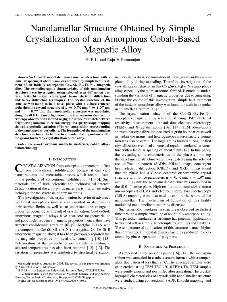
Fig. 1. Nanolameller structure at various stages of phase transformation:(a) initial stages of crystallization; (b) crystallization is complete; and (c), (d)crystals containing nanolamellar structure are partially consumed.
CBED techniques. HRTEM and EELS mapping were also usedto characterize the nanolamellar structure. X-ray analysis wasperformed using a PANalytical high resolution XRD (PANalyt-ical’s X’Pert PRO Extended MRD system) with Cr tube (wave-length of 0.229 360 6 nm).
III. RESULTS AND DISCUSSION
A. Nanolamellar Structure and Crystallography
The nanolamellar structure observed in this investigation is anew member of the nanostructures [1]–[3], [18], [19] formed bycrystallization from amorphous precursors. It is observed withincrystals formed during heat treatment of the amorphous matrix[17]. Fig. 1 shows the nanolamellar structure at different stagesof microstructural evolution following heat treatment at temper-atures of 500 C and 530 C. This nanolamellar structure is ob-served within large crystals in the amorphous matrix [Fig. 1(a)].Such crystals consumed the amorphous matrix after heat treat-ment for longer heat treatment time or at higher temperatures[16], [17]; a typical result is shown in Fig. 1(b). Some fine pre-cipitates can also be observed at grain boundaries in Fig. 1(b).Subsequent transformation, which was initiated from the grainboundaries, occurred after heat treatment for even longer time orat higher temperatures; discontinuous coarsening was observed,but the remaining nanolamellar structure [Fig. 1(c) and (d)] stillmaintained its periodicity, indicating high thermal stability.
The composition of the crystal with the nanolamellar structurewas considered to be close to that of the original amorphousmatrix, since these crystals were the main microstructural con-stituent and only a small volume fraction of fine precipitates atthe grain boundaries were observed. HRTEM of the nanolamellar
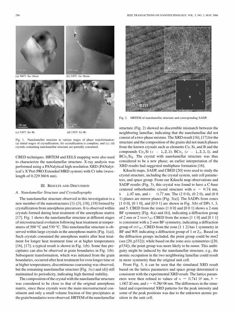
Fig. 2. HRTEM of nanolamellar structure and corresponding SADP.
structure (Fig. 2) showed no discernible mismatch between theneighboring lamellae, indicating that the nanolamellae did notconsist of a two-phase mixture. The XRD result [16], [17] for thestructure and the composition of the grains did not match phasesfrom the known crystals such as elements Co, Si, and B and thecompounds Co Si ( ), BCo ( ), andBCo Si . The crystal with nanolamellar structure was thusconsidered to be a new phase; an earlier interpretation of theXRD results had suggested multiphase formation [16].
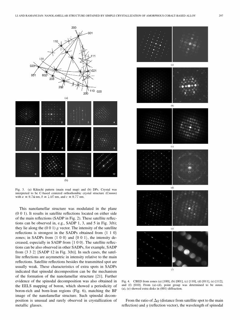
Kikuchi maps, SADP, and CBED [20] were used to study thecrystal structure, including the crystal system, unit cell parame-ters, and space group. From our Kikuchi map observations andSADP results (Fig. 3), this crystal was found to have a C-basecentered orthorhombic crystal structure with nm,
nm, and nm. The (2 0 0), (0 2 0), and (0 01) planes are mirror planes [Fig. 3(a)]. The SADPs from zones[1 0 0], [0 1 0], and [0 0 1] are shown in Fig. 3(b) of DPs 1, 3,and 5. CBED from the zones [1 0 0] and [0 0 1] shows a 2-mmBF symmetry [Fig. 4(a) and (b)], indicating a diffraction groupof 2 mm or 2 ; CBED from the zones [1 1 0] and [0 1 1]is consistent with a 2-mm BF symmetry, indicating a diffractiongroup of .; CBED from the zone [1 1 2] has 1 symmetry inBF and WP, indicating a diffraction group of 1 or . Based onthe diffraction groups included, the point group could be mm2(see [20, p332]); while based on the zone-axis symmetries ([20,p334]), the point group was more likely to be mmm. This ambi-guity might be induced by the nanolamellar structure, e.g., theatomic occupation in the two neighboring lamellae could resultin more symmetry than the original unit cell.
From Fig. 5, it can be seen that the simulated XRD resultbased on the lattice parameters and space group determined isconsistent with the experimental XRD result. The lattice param-eters were then refined to values of nm,
nm, and nm. The differences in the simu-lated and experimental XRD patterns for the peak intensity andsome of the peak positions was due to the unknown atomic po-sition in the unit cell.
LI AND RAMANUJAN: NANOLAMELLAR STRUCTURE OBTAINED BY SIMPLE CRYSTALLIZATION OF AMORPHOUS COBALT-BASED ALLOY 297
Fig. 3. (a) Kikuchi pattern (main road map) and (b) DPs. Crystal wasinterpreted to be C-based centered orthorhombic crystal structure (Cmmm)with a = 0:74 nm, b = 1:07 nm, and c = 0:77 nm.
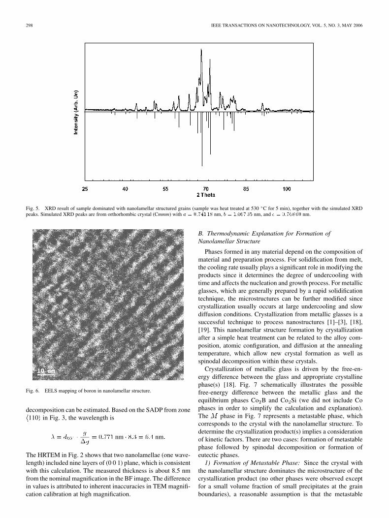
This nanolamellar structure was modulated in the plane(0 0 1). It results in satellite reflections located on either sideof the main reflections (SADP in Fig. 2). These satellite reflec-tions can be observed in, e.g., SADP 1, 3, and 5 in Fig. 3(b);they lie along the (0 0 1) vector. The intensity of the satellitereflections is strongest in the SADPs obtained from 1 1 0zones; in SADPs from 1 0 0 and 0 0 1 , the intensity de-creased, especially in SADP from 1 0 0 . The satellite reflec-tions can be also observed in other SADPs, for example, SADPfrom 3 3 2 [SADP 12 in Fig. 3(b)]. In such cases, the satel-lite reflections are asymmetric in intensity relative to the mainreflections. Satellite reflections besides the transmitted spot areusually weak. These characteristics of extra spots in SADPsindicated that spinodal decomposition can be the mechanismof the formation of the nanolamellar structure [21]. Furtherevidence of the spinodal decomposition was also obtained inthe EELS mapping of boron, which showed a periodicity ofboron-rich and born-lean regions (Fig. 6), matching the BFimage of the nanolamellar structure. Such spinodal decom-position is unusual and rarely observed in crystallization ofmetallic glasses.
Fig. 4. CBED from zones (a) [100], (b) [001], (c) [110], (d) [011], (e) [112],and (f) [010]. From (a)–(d), point group was determined to be mmm.(a), (e) showed extra disks in (001) diffraction.
From the ratio of (distance from satellite spot to the mainreflection) and (reflection vector), the wavelength of spinodal
298 IEEE TRANSACTIONS ON NANOTECHNOLOGY, VOL. 5, NO. 3, MAY 2006
Fig. 5. XRD result of sample dominated with nanolamellar structured grains (sample was heat treated at 530 C for 5 min), together with the simulated XRDpeaks. Simulated XRD peaks are from orthorhombic crystal (Cmmm) with a = 0:74118 nm, b = 1:06735 nm, and c = 0:76800 nm.
Fig. 6. EELS mapping of boron in nanolamellar structure.
decomposition can be estimated. Based on the SADP from zone110 in Fig. 3, the wavelength is
nm nm
The HRTEM in Fig. 2 shows that two nanolamellae (one wave-length) included nine layers of (0 0 1) plane, which is consistentwith this calculation. The measured thickness is about 8.5 nmfrom the nominal magnification in the BF image. The differencein values is attributed to inherent inaccuracies in TEM magnifi-cation calibration at high magnification.
B. Thermodynamic Explanation for Formation ofNanolamellar Structure
Phases formed in any material depend on the composition ofmaterial and preparation process. For solidification from melt,the cooling rate usually plays a significant role in modifying theproducts since it determines the degree of undercooling withtime and affects the nucleation and growth process. For metallicglasses, which are generally prepared by a rapid solidificationtechnique, the microstructures can be further modified sincecrystallization usually occurs at large undercooling and slowdiffusion conditions. Crystallization from metallic glasses is asuccessful technique to process nanostructures [1]–[3], [18],[19]. This nanolamellar structure formation by crystallizationafter a simple heat treatment can be related to the alloy com-position, atomic configuration, and diffusion at the annealingtemperature, which allow new crystal formation as well asspinodal decomposition within these crystals.
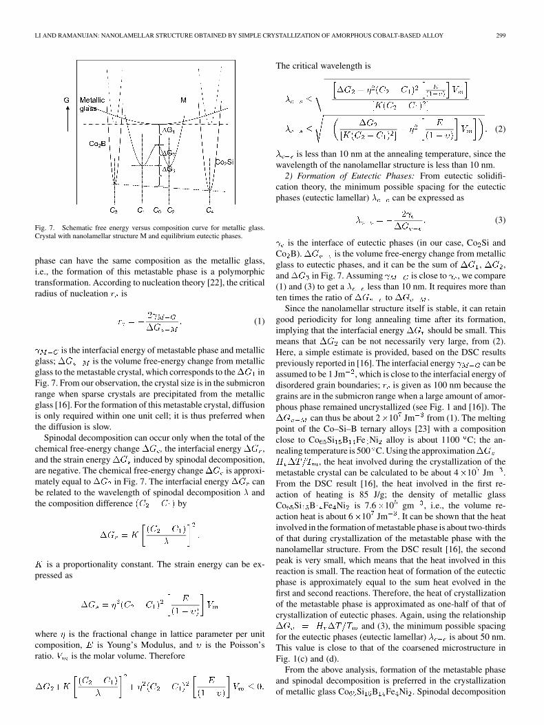
Crystallization of metallic glass is driven by the free-en-ergy difference between the glass and appropriate crystallinephase(s) [18]. Fig. 7 schematically illustrates the possiblefree-energy difference between the metallic glass and theequilibrium phases Co B and Co Si (we did not include Cophases in order to simplify the calculation and explanation).The phase in Fig. 7 represents a metastable phase, whichcorresponds to the crystal with the nanolamellar structure. Todetermine the crystallization product(s) implies a considerationof kinetic factors. There are two cases: formation of metastablephase followed by spinodal decomposition or formation ofeutectic phases.
1) Formation of Metastable Phase: Since the crystal withthe nanolamellar structure dominates the microstructure of thecrystallization product (no other phases were observed exceptfor a small volume fraction of small precipitates at the grainboundaries), a reasonable assumption is that the metastable
LI AND RAMANUJAN: NANOLAMELLAR STRUCTURE OBTAINED BY SIMPLE CRYSTALLIZATION OF AMORPHOUS COBALT-BASED ALLOY 299
Fig. 7. Schematic free energy versus composition curve for metallic glass.Crystal with nanolamellar structure M and equilibrium eutectic phases.
phase can have the same composition as the metallic glass,i.e., the formation of this metastable phase is a polymorphictransformation. According to nucleation theory [22], the criticalradius of nucleation is
(1)
is the interfacial energy of metastable phase and metallicglass; is the volume free-energy change from metallicglass to the metastable crystal, which corresponds to the inFig. 7. From our observation, the crystal size is in the submicronrange when sparse crystals are precipitated from the metallicglass [16]. For the formation of this metastable crystal, diffusionis only required within one unit cell; it is thus preferred whenthe diffusion is slow.
Spinodal decomposition can occur only when the total of thechemical free-energy change , the interfacial energy ,and the strain energy induced by spinodal decomposition,are negative. The chemical free-energy change is approxi-mately equal to in Fig. 7. The interfacial energy canbe related to the wavelength of spinodal decomposition andthe composition difference by
is a proportionality constant. The strain energy can be ex-pressed as
where is the fractional change in lattice parameter per unitcomposition, is Young’s Modulus, and is the Poisson’sratio. is the molar volume. Therefore
The critical wavelength is
(2)
is less than 10 nm at the annealing temperature, since thewavelength of the nanolamellar structure is less than 10 nm.
2) Formation of Eutectic Phases: From eutectic solidifi-cation theory, the minimum possible spacing for the eutecticphases (eutectic lamellar) can be expressed as
(3)
is the interface of eutectic phases (in our case, Co Si andCo B). is the volume free-energy change from metallicglass to eutectic phases, and it can be the sum of , ,and in Fig. 7. Assuming is close to , we compare(1) and (3) to get a less than 10 nm. It requires more thanten times the ratio of to .
Since the nanolamellar structure itself is stable, it can retaingood periodicity for long annealing time after its formation,implying that the interfacial energy should be small. Thismeans that can be not necessarily very large, from (2).Here, a simple estimate is provided, based on the DSC resultspreviously reported in [16]. The interfacial energy can beassumed to be 1 Jm , which is close to the interfacial energy ofdisordered grain boundaries; is given as 100 nm because thegrains are in the submicron range when a large amount of amor-phous phase remained uncrystallized (see Fig. 1 and [16]). The
can thus be about 2 10 Jm from (1). The meltingpoint of the Co–Si–B ternary alloys [23] with a compositionclose to Co Si B Fe Ni alloy is about 1100 C; the an-nealing temperature is 500 C. Using the approximation
, the heat involved during the crystallization of themetastable crystal can be calculated to be about 4 10 Jm .From the DSC result [16], the heat involved in the first re-action of heating is 85 J/g; the density of metallic glassCo Si B Fe Ni is 7.6 10 gm , i.e., the volume re-action heat is about 6 10 Jm . It can be shown that the heatinvolved in the formation of metastable phase is about two-thirdsof that during crystallization of the metastable phase with thenanolamellar structure. From the DSC result [16], the secondpeak is very small, which means that the heat involved in thisreaction is small. The reaction heat of formation of the eutecticphase is approximately equal to the sum heat evolved in thefirst and second reactions. Therefore, the heat of crystallizationof the metastable phase is approximated as one-half of that ofcrystallization of eutectic phases. Again, using the relationship
and (3), the minimum possible spacingfor the eutectic phases (eutectic lamellar) is about 50 nm.This value is close to that of the coarsened microstructure inFig. 1(c) and (d).
From the above analysis, formation of the metastable phaseand spinodal decomposition is preferred in the crystallizationof metallic glass Co Si B Fe Ni . Spinodal decomposition
300 IEEE TRANSACTIONS ON NANOTECHNOLOGY, VOL. 5, NO. 3, MAY 2006
can happen almost simultaneously with metastable crystal for-mation since it only involves 8 9 layers of unit cells. That thenanolamellar structure is modulated in the plane of (0 0 1) maybe attributed to the larger interfacial energy for the interfacesperpendicular to the (0 0 1) plane. This microstructure can alsobe modified by annealing conditions, for example, using largeheating rate and annealing at high temperature. The formationof the metastable crystal may be bypassed due to the highermobility of atoms, leading to the formation of the equilibriumphases.
This crystallization process is highly alloy compositiondependent. For compositions outside the spinodal region, thefine nanolamellar structure cannot be formed; stable phasesare crystallized more easily. For example, in the crystalliza-tion of Co Fe Si B metallic glass [24], a mutiphasemicrostructure with submicron dimensions, was formed.
IV. CONCLUSION
An unusual highly periodic nanolamellar structure with aspacing of about 5 nm was observed during the crystallizationof a Co-based Co Si B Fe Ni amorphous magnetic alloy.The crystallographic characteristics of this microstructure wereinvestigated using SADP, Kikuchi mapping, CBED, and XRD.HRTEM and EELS mapping were also used to explore thenature of the nanolamellae.
1 ) The grain with nanolamellar structure has a C-base cen-tered orthorhombic crystal structure with nm,
nm, and nm. The nanolamellar struc-ture was modulated in the plane of (0 0 1).
2 ) Satellite reflection spots were observed in the SADPs, andboron partitioning in the neighboring nanolamellae wasobserved in the EELS mapping. Thus, spinodal decom-position by boron partitioning was considered to be themechanism of formation of this nanolamellar structure.
3 ) The wavelength of the spinodal decomposition was cal-culated to be 6.4 nm, which involved about nine layers ofthe unit cell; this result was consistent with the TEM andHRTEM observations.
4 ) The formation of the grains with a nanolamellar structurewas found to be more kinetically favorable than the usualcrystallization of the eutectic phases.
ACKNOWLEDGMENT
The authors would like to thank Mr. P. C. Lim, Dr. Z. L. Dong,and Dr. J. Plévert for their help in the XRD experiments and theXRD data analysis. They would like to thank Dr. Y. L. Foo, fromthe Institute of Materials Research and Engineering, Singapore,for his help in obtaining the EELS data.
REFERENCES
[1] M. E. McHenry, M. A. Willard, and D. E. Laughlin, Prog. Mater. Sci.,vol. 44, p. 291, 1999.
[2] W. J. Botta F, D. Negri, and A. R. Yavari, J. Non-Cryst. Sol., vol. 247,p. 19, 1999.
[3] R. Janlewing and U. Köster, Mater. Sci. Eng. A, vol. 304–306, p. 833,2001.
[4] Y. Takahar and H. Matsuda, Mater. Trans., JIM, vol. 36, no. 7, p. 903,1995.
[5] D. G. Morris, Acta Metall., vol. 29, p. 1213, 1981.[6] C. Gomez-Polo, E. Pulido, G. Rivero, and A. Hernando, J. Appl. Phys.,
vol. 4984, 1990.[7] C. K. Kim and R. C. O’Handley, Metall. Mater. Trans. A, vol. 28A, p.
423, 1997.[8] M. Coisson, P. Tiberto, and F. Vinai, J. Magn. Magn. Mater., vol.
242–245, p. 288, 2002.[9] N. H. Nghi, N. M. Hong, Z. Q. Vinh, N. V. Dung, and P. M. Hong, Phys.
B, vol. 327, p. 253, 2003.[10] G. Buttino, A. Cecchetti, and M. Poppi, J. Magn. Magn. Mater., vol. 172,
p. 147, 1997.[11] G. Bordin, G. Buttino, A. Cecchetti, and M. Poppi, J. Magn. Magn.
Mater., vol. 195, p. 583, 1999.[12] S. S. Yoon, C. G. Kim, H. C. Kim, K. J. Jang, and D. Y. Kim, J. Magn.
Magn. Mater., vol. 196–197, p. 843, 1999.[13] J. H. Yang, Y. B. Kim, K. S. Ryu, M. J. Kim, Y. C. Chung, and T. K.
Kim, J. Magn. Magn. Mater., vol. 222, p. 65, 2000.[14] C. S. Tsai, W. J. Yang, M. S. Leu, and C. S. Lin, J. Appl. Phys., vol. 70,
no. 10, p. 5846, 1991.[15] P. Quintana, E. Amano, R. Valenzuela, and J. T. S. Irvine, J. Appl. Phys.,
vol. 75, no. 10, p. 6940, 1994.[16] H. F. Li and R. V. Ramanujan, Mater. Sci. Eng. A, vol. 375–377, p. 1087,
2004.[17] , Intermetallics, vol. 12, no. 7–9, p. 803, 2004.[18] M. G. Scott, “Crystallization,” in Amorphous Metallic Alloys, F. E.
Luborsky, Ed. London, U.K.: Butterworth, 1983, vol. 144, Butter-worths monographs in materials.
[19] Y. Gao, S. Zhang, and B. Liu, J. Magn. Magn. Mater., vol. 208, p. 158,2000.
[20] D. B. William and C. B. Carter, Transmission Electron Microscopy: ATextbook for Materials Science. New York: Plenum, 1996.
[21] J. W. Edington, Electron Diffraction in the Electron Microscope: PhilipsTechnical Library, Monographs in Practical Electron Microscopy in Ma-terials Science, p. 63.
[22] D. A. Porter and K. E. Easterling, Phase Transformations in Metals andAlloys, 2nd ed. London, U.K.: Chapman and Hall, 1992.
[23] P. Villars, A. Prince, and H. Okamoto, Handbook of Ternary Alloy PhaseDiagrams, ASM Int., Materials Park, OH, 1997.
[24] I. C. Rho, C. S. Yoon, C. K. Kim, T. Y. Byun, and K. S. Hong, Mater.Sci. Eng. B, vol. B96, p. 48, 2002.
H. F. Li received the B.Eng. degree in materialsscience and engineering from Huazhong Universityof Science and Technology, China, in 2001, andthe Ph.D. degree from Nanyang TechnologicalUniversity, Singapore, in 2006.
She worked on gallium nitride microelectronicmaterials as a Research Staff Member at NanyangTechnological University from 2005 to 2006.Currently, she is a Visiting Research Scholar atRensselaer Polytechnic Institute, Troy, NY. Herresearch interests include magnetic materials, mi-
croelectronic materials, nanostructures, transmission electron microscopycharacterization, and mechanical alloying.
Raju V. Ramanujan received the B.Tech. degreefrom the Indian Institute of Technology, India, andthe M.Engg. and Ph.D. degrees in materials sciencefrom Carnegie Mellon University, Pittsburgh, PA.
He has held research positions in the U.K. andIndia and is currently an Associate Professor inthe School of Materials Science and Engineering,Nanyang Technological University, Singapore. Hiscurrent research interests include nanotechnology,magnetic materials, and the application of nanoma-terials in bioengineering.
Dr. Ramanujan serves on the Editorial Board or is Associate Editor of severaljournals and is a member of MRS, TMS, ASM. He is the Secretary of the Insti-tute of Materials (East Asia). He has organized international conferences in theareas of advanced functional materials, nanomaterials, and biomaterials.