tms320x2833x, 2823x multichannel buffered serial...
TRANSCRIPT
TMS320F2833x/2823xMultichannel Buffered Serial Port (McBSP)
Reference Guide
Literature Number: SPRUFB7B
September 2007–Revised August 2011

2 SPRUFB7B–September 2007–Revised August 2011Submit Documentation Feedback
Copyright © 2007–2011, Texas Instruments Incorporated
Contents
Preface ...................................................................................................................................... 13
1 Overview .......................................................................................................................... 151.1 Brief Description ........................................................................................................... 161.2 Features of the McBSPs .................................................................................................. 161.3 McBSP Pins/Signals ...................................................................................................... 17
1.3.1 McBSP Generic Block Diagram ................................................................................ 18
2 McBSP Operation .............................................................................................................. 192.1 Data Transfer Process of McBSPs ...................................................................................... 20
2.1.1 Data Transfer Process for Word Length of 8, 12, or 16 Bits ................................................ 202.1.2 Data Transfer Process for Word Length of 20, 24, or 32 Bits .............................................. 20
2.2 Companding (Compressing and Expanding) Data .................................................................... 202.2.1 Companding Formats ............................................................................................ 212.2.2 Capability to Compand Internal Data .......................................................................... 212.2.3 Reversing Bit Order: Option to Transfer LSB First ........................................................... 22
2.3 Clocking and Framing Data .............................................................................................. 222.3.1 Clocking ............................................................................................................ 222.3.2 Serial Words ...................................................................................................... 222.3.3 Frames and Frame Synchronization ........................................................................... 232.3.4 Generating Transmit and Receive Interrupts ................................................................. 232.3.5 Ignoring Frame-Synchronization Pulses ....................................................................... 232.3.6 Frame Frequency ................................................................................................. 242.3.7 Maximum Frame Frequency .................................................................................... 24
2.4 Frame Phases ............................................................................................................. 242.4.1 Number of Phases, Words, and Bits Per Frame ............................................................. 252.4.2 Single-Phase Frame Example .................................................................................. 252.4.3 Dual-Phase Frame Example .................................................................................... 252.4.4 Implementing the AC97 Standard With a Dual-Phase Frame .............................................. 26
2.5 McBSP Reception ......................................................................................................... 262.6 McBSP Transmission ..................................................................................................... 292.7 Interrupts and DMA Events Generated by a McBSP ................................................................. 30
3 McBSP Sample Rate Generator ........................................................................................... 313.1 Block Diagram ............................................................................................................. 32
3.1.1 Clock Generation in the Sample Rate Generator ............................................................ 333.1.2 Choosing an Input Clock ........................................................................................ 333.1.3 Choosing a Polarity for the Input Clock ........................................................................ 333.1.4 Choosing a Frequency for the Output Clock (CLKG) ........................................................ 343.1.5 Keeping CLKG Synchronized to External MCLKR ........................................................... 34
3.2 Frame Synchronization Generation in the Sample Rate Generator ................................................ 353.2.1 Choosing the Width of the Frame-Synchronization Pulse on FSG ........................................ 353.2.2 Controlling the Period Between the Starting Edges of Frame-Synchronization Pulses on FSG ....... 353.2.3 Keeping FSG Synchronized to an External Clock ........................................................... 35
3.3 Synchronizing Sample Rate Generator Outputs to an External Clock ............................................. 353.3.1 Operating the Transmitter Synchronously with the Receiver ............................................... 363.3.2 Synchronization Examples ...................................................................................... 36
3.4 Reset and Initialization Procedure for the Sample Rate Generator ................................................. 37
3SPRUFB7B–September 2007–Revised August 2011 ContentsSubmit Documentation Feedback
Copyright © 2007–2011, Texas Instruments Incorporated
www.ti.com
4 McBSP Exception/Error Conditions ..................................................................................... 394.1 Types of Errors ............................................................................................................ 404.2 Overrun in the Receiver .................................................................................................. 40
4.2.1 Example of Overrun Condition .................................................................................. 414.2.2 Example of Preventing Overrun Condition .................................................................... 41
4.3 Unexpected Receive Frame-Synchronization Pulse .................................................................. 414.3.1 Possible Responses to Receive Frame-Synchronization Pulses .......................................... 414.3.2 Example of Unexpected Receive Frame-Synchronization Pulse .......................................... 434.3.3 Preventing Unexpected Receive Frame-Synchronization Pulses .......................................... 43
4.4 Overwrite in the Transmitter ............................................................................................. 444.4.1 Example of Overwrite Condition ................................................................................ 444.4.2 Preventing Overwrites ........................................................................................... 44
4.5 Underflow in the Transmitter ............................................................................................. 444.5.1 Example of the Underflow Condition ........................................................................... 454.5.2 Example of Preventing Underflow Condition .................................................................. 45
4.6 Unexpected Transmit Frame-Synchronization Pulse ................................................................. 454.6.1 Possible Responses to Transmit Frame-Synchronization Pulses .......................................... 454.6.2 Example of Unexpected Transmit Frame-Synchronization Pulse .......................................... 474.6.3 Preventing Unexpected Transmit Frame-Synchronization Pulses ......................................... 47
5 Multichannel Selection Modes ............................................................................................. 495.1 Channels, Blocks, and Partitions ........................................................................................ 505.2 Multichannel Selection .................................................................................................... 515.3 Configuring a Frame for Multichannel Selection ...................................................................... 515.4 Using Two Partitions ...................................................................................................... 51
5.4.1 Assigning Blocks to Partitions A and B ........................................................................ 515.4.2 Reassigning Blocks During Reception/Transmission ........................................................ 52
5.5 Using Eight Partitions ..................................................................................................... 535.6 Receive Multichannel Selection Mode .................................................................................. 545.7 Transmit Multichannel Selection Modes ................................................................................ 54
5.7.1 Disabling/Enabling Versus Masking/Unmasking ............................................................. 555.7.2 Activity on McBSP Pins for Different Values of XMCM ...................................................... 55
5.8 Using Interrupts Between Block Transfers ............................................................................. 56
6 SPI Operation Using the Clock Stop Mode ............................................................................ 596.1 SPI Protocol ................................................................................................................ 606.2 Clock Stop Mode .......................................................................................................... 606.3 Bits Used to Enable and Configure the Clock Stop Mode ........................................................... 606.4 Clock Stop Mode Timing Diagrams ..................................................................................... 616.5 Procedure for Configuring a McBSP for SPI Operation .............................................................. 636.6 McBSP as the SPI Master ................................................................................................ 636.7 McBSP as an SPI Slave .................................................................................................. 65
7 Receiver Configuration ...................................................................................................... 677.1 Programming the McBSP Registers for the Desired Receiver Operation ......................................... 687.2 Resetting and Enabling the Receiver ................................................................................... 68
7.2.1 Reset Considerations ............................................................................................ 697.3 Set the Receiver Pins to Operate as McBSP Pins .................................................................... 697.4 Enable/Disable the Digital Loopback Mode ............................................................................ 69
7.4.1 Digital Loopback Mode .......................................................................................... 707.5 Enable/Disable the Clock Stop Mode ................................................................................... 70
7.5.1 Clock Stop Mode ................................................................................................. 707.6 Enable/Disable the Receive Multichannel Selection Mode .......................................................... 717.7 Choose One or Two Phases for the Receive Frame ................................................................. 717.8 Set the Receive Word Length(s) ........................................................................................ 72
4 Contents SPRUFB7B–September 2007–Revised August 2011Submit Documentation Feedback
Copyright © 2007–2011, Texas Instruments Incorporated
www.ti.com
7.8.1 Word Length Bits ................................................................................................. 727.9 Set the Receive Frame Length .......................................................................................... 72
7.9.1 Selected Frame Length .......................................................................................... 737.10 Enable/Disable the Receive Frame-Synchronization Ignore Function ............................................. 73
7.10.1 Unexpected Frame-Synchronization Pulses and the Frame-Synchronization Ignore Function ....... 737.10.2 Examples of Effects of RFIG ................................................................................... 74
7.11 Set the Receive Companding Mode .................................................................................... 747.11.1 Companding ...................................................................................................... 757.11.2 Format of Expanded Data ...................................................................................... 757.11.3 Companding Internal Data ..................................................................................... 757.11.4 Option to Receive LSB First ................................................................................... 75
7.12 Set the Receive Data Delay .............................................................................................. 757.12.1 Data Delay ....................................................................................................... 767.12.2 0-Bit Data Delay ................................................................................................. 767.12.3 2-Bit Data Delay ................................................................................................. 76
7.13 Set the Receive Sign-Extension and Justification Mode ............................................................. 777.13.1 Sign-Extension and the Justification .......................................................................... 77
7.14 Set the Receive Interrupt Mode ......................................................................................... 797.15 Set the Receive Frame-Synchronization Mode ........................................................................ 79
7.15.1 Receive Frame-Synchronization Modes ...................................................................... 797.16 Set the Receive Frame-Synchronization Polarity ..................................................................... 81
7.16.1 Frame-Synchronization Pulses, Clock Signals, and Their Polarities ..................................... 817.16.2 Frame-Synchronization Period and the Frame-Synchronization Pulse Width ........................... 82
7.17 Set the Receive Clock Mode ............................................................................................. 837.17.1 Selecting a Source for the Receive Clock and a Data Direction for the MCLKR Pin .................. 84
7.18 Set the Receive Clock Polarity .......................................................................................... 847.18.1 Frame Synchronization Pulses, Clock Signals, and Their Polarities ..................................... 85
7.19 Set the SRG Clock Divide-Down Value ................................................................................ 857.19.1 Sample Rate Generator Clock Divider ........................................................................ 86
7.20 Set the SRG Clock Synchronization Mode ............................................................................. 867.21 Set the SRG Clock Mode (Choose an Input Clock) ................................................................... 86
7.21.1 SRG Clock Mode ................................................................................................ 877.22 Set the SRG Input Clock Polarity ........................................................................................ 88
7.22.1 Using CLKXP/CLKRP to Choose an Input Clock Polarity ................................................. 88
8 Transmitter Configuration .................................................................................................. 898.1 Programming the McBSP Registers for the Desired Transmitter Operation ...................................... 908.2 Resetting and Enabling the Transmitter ................................................................................ 90
8.2.1 Reset Considerations ............................................................................................ 918.3 Set the Transmitter Pins to Operate as McBSP Pins ................................................................. 918.4 Enable/Disable the Digital Loopback Mode ............................................................................ 91
8.4.1 Digital Loopback Mode .......................................................................................... 918.5 Enable/Disable the Clock Stop Mode ................................................................................... 92
8.5.1 Clock Stop Mode ................................................................................................. 928.6 Enable/Disable Transmit Multichannel Selection ...................................................................... 938.7 Choose One or Two Phases for the Transmit Frame ................................................................ 948.8 Set the Transmit Word Length(s) ........................................................................................ 94
8.8.1 Word Length Bits ................................................................................................. 948.9 Set the Transmit Frame Length ......................................................................................... 95
8.9.1 Selected Frame Length .......................................................................................... 958.10 Enable/Disable the Transmit Frame-Synchronization Ignore Function ............................................. 96
8.10.1 Unexpected Frame-Synchronization Pulses and Frame-Synchronization Ignore ...................... 968.10.2 Examples Showing the Effects of XFIG ...................................................................... 96
8.11 Set the Transmit Companding Mode ................................................................................... 97
5SPRUFB7B–September 2007–Revised August 2011 ContentsSubmit Documentation Feedback
Copyright © 2007–2011, Texas Instruments Incorporated
www.ti.com
8.11.1 Companding ...................................................................................................... 978.11.2 Format for Data To Be Compressed .......................................................................... 978.11.3 Capability to Compand Internal Data ......................................................................... 988.11.4 Option to Transmit LSB First ................................................................................... 98
8.12 Set the Transmit Data Delay ............................................................................................. 988.12.1 Data Delay ....................................................................................................... 988.12.2 0-Bit Data Delay ................................................................................................. 998.12.3 2-Bit Data Delay ................................................................................................. 99
8.13 Set the Transmit DXENA Mode ........................................................................................ 1008.13.1 DXENA Mode ................................................................................................... 100
8.14 Set the Transmit Interrupt Mode ....................................................................................... 1008.15 Set the Transmit Frame-Synchronization Mode ..................................................................... 101
8.15.1 Transmit Frame-Synchronization Modes ................................................................... 1018.15.2 Other Considerations .......................................................................................... 101
8.16 Set the Transmit Frame-Synchronization Polarity ................................................................... 1028.16.1 Frame Synchronization Pulses, Clock Signals, and Their Polarities .................................... 102
8.17 Set the SRG Frame-Synchronization Period and Pulse Width .................................................... 1038.17.1 Frame-Synchronization Period and Frame-Synchronization Pulse Width .............................. 103
8.18 Set the Transmit Clock Mode .......................................................................................... 1048.18.1 Selecting a Source for the Transmit Clock and a Data Direction for the MCLKX pin ................. 1048.18.2 Other Considerations .......................................................................................... 104
8.19 Set the Transmit Clock Polarity ........................................................................................ 1048.19.1 Frame Synchronization Pulses, Clock Signals, and Their Polarities .................................... 105
9 Emulation and Reset Considerations ................................................................................. 1079.1 McBSP Emulation Mode ................................................................................................ 1089.2 Resetting and Initializing McBSPs ..................................................................................... 108
9.2.1 McBSP Pin States: DSP Reset Versus Receiver/Transmitter Reset .................................... 1089.2.2 Device Reset, McBSP Reset, and Sample Rate Generator Reset ....................................... 1089.2.3 McBSP Initialization Procedure ............................................................................... 1099.2.4 Resetting the Transmitter While the Receiver is Running ................................................. 110
10 Data Packing Examples .................................................................................................... 11110.1 Data Packing Using Frame Length and Word Length .............................................................. 11210.2 Data Packing Using Word Length and the Frame-Synchronization Ignore Function ........................... 113
11 McBSP Registers ............................................................................................................. 11511.1 Register Summary ....................................................................................................... 11611.2 Data Receive Registers (DRR[1,2]) ................................................................................... 116
11.2.1 Data Travel From Data Receive Pins to the Registers ................................................... 11711.3 Data Transmit Registers (DXR[1,2]) ................................................................................... 118
11.3.1 Data Travel From Registers to Data Transmit (DX) Pins ................................................. 11811.4 Serial Port Control Registers (SPCR[1,2]) ............................................................................ 118
11.4.1 Serial Port Control 1 Register (SPCR1) .................................................................... 11811.4.2 Serial Port Control 2 Register (SPCR2) .................................................................... 121
11.5 Receive Control Registers (RCR[1, 2]) ............................................................................... 12311.5.1 Receive Control Register 1 (RCR1) ......................................................................... 12311.5.2 Receive Control Register 2 (RCR2) ......................................................................... 124
11.6 Transmit Control Registers (XCR1 and XCR2) ...................................................................... 12511.6.1 Transmit Control 1 Register (XCR1) ........................................................................ 12611.6.2 Transmit Control 2 Register (XCR2) ........................................................................ 127
11.7 Sample Rate Generator Registers (SRGR1 and SRGR2) ......................................................... 12811.7.1 Sample Rate Generator 1 Register (SRGR1) .............................................................. 12811.7.2 Sample Rate Generator 2 Register (SRGR2) .............................................................. 129
11.8 Multichannel Control Registers (MCR[1,2]) ........................................................................... 13111.8.1 Multichannel Control 1 Register (MCR1) ................................................................... 131
6 Contents SPRUFB7B–September 2007–Revised August 2011Submit Documentation Feedback
Copyright © 2007–2011, Texas Instruments Incorporated
www.ti.com
11.8.2 Multichannel Control 2 Register (MCR2) ................................................................... 13311.9 Pin Control Register (PCR) ............................................................................................. 13511.10 Receive Channel Enable Registers (RCERA, RCERB, RCERC, RCERD, RCERE, RCERF, RCERG,
RCERH) ................................................................................................................... 13711.10.1 RCERs Used in the Receive Multichannel Selection Mode ............................................ 138
11.11 Transmit Channel Enable Registers (XCERA, XCERB, XCERC, XCERD, XCERE, XCERF, XCERG,XCERH) ................................................................................................................... 13911.11.1 XCERs Used in a Transmit Multichannel Selection Mode .............................................. 140
11.12 Interrupt Generation ..................................................................................................... 14111.12.1 McBSP Receive Interrupt Generation ..................................................................... 14211.12.2 McBSP Transmit Interrupt Generation ..................................................................... 14211.12.3 Error Flags .................................................................................................... 14311.12.4 McBSP Interrupt Enable Register .......................................................................... 143
11.13 McBSP Modes ........................................................................................................... 143
A Revision History .............................................................................................................. 145
7SPRUFB7B–September 2007–Revised August 2011 ContentsSubmit Documentation Feedback
Copyright © 2007–2011, Texas Instruments Incorporated
www.ti.com
List of Figures
1-1. Conceptual Block Diagram of the McBSP ............................................................................. 18
2-1. McBSP Data Transfer Paths ............................................................................................. 20
2-2. Companding Processes .................................................................................................. 21
2-3. μ-Law Transmit Data Companding Format ............................................................................ 21
2-4. A-Law Transmit Data Companding Format ............................................................................ 21
2-5. Two Methods by Which the McBSP Can Compand Internal Data .................................................. 22
2-6. Example - Clock Signal Control of Bit Transfer Timing............................................................... 22
2-7. McBSP Operating at Maximum Packet Frequency ................................................................... 24
2-8. Single-Phase Frame for a McBSP Data Transfer ..................................................................... 25
2-9. Dual-Phase Frame for a McBSP Data Transfer ....................................................................... 25
2-10. Implementing the AC97 Standard With a Dual-Phase Frame ....................................................... 26
2-11. Timing of an AC97-Standard Data Transfer Near Frame Synchronization ........................................ 26
2-12. McBSP Reception Physical Data Path ................................................................................. 27
2-13. McBSP Reception Signal Activity ....................................................................................... 27
2-14. McBSP Transmission Physical Data Path ............................................................................. 29
2-15. McBSP Transmission Signal Activity ................................................................................... 29
3-1. Conceptual Block Diagram of the Sample Rate Generator .......................................................... 32
3-2. Possible Inputs to the Sample Rate Generator and the Polarity Bits............................................... 34
3-3. CLKG Synchronization and FSG Generation When GSYNC = 1 and CLKGDV = 1 ............................. 36
3-4. CLKG Synchronization and FSG Generation When GSYNC = 1 and CLKGDV = 3 ............................. 37
4-1. Overrun in the McBSP Receiver ........................................................................................ 41
4-2. Overrun Prevented in the McBSP Receiver ........................................................................... 41
4-3. Possible Responses to Receive Frame-Synchronization Pulses ................................................... 42
4-4. An Unexpected Frame-Synchronization Pulse During a McBSP Reception ...................................... 43
4-5. Proper Positioning of Frame-Synchronization Pulses ................................................................ 43
4-6. Data in the McBSP Transmitter Overwritten and Thus Not Transmitted........................................... 44
4-7. Underflow During McBSP Transmission ............................................................................... 45
4-8. Underflow Prevented in the McBSP Transmitter ...................................................................... 45
4-9. Possible Responses to Transmit Frame-Synchronization Pulses .................................................. 46
4-10. An Unexpected Frame-Synchronization Pulse During a McBSP Transmission .................................. 47
4-11. Proper Positioning of Frame-Synchronization Pulses ................................................................ 47
5-1. Alternating Between the Channels of Partition A and the Channels of Partition B ............................... 52
5-2. Reassigning Channel Blocks Throughout a McBSP Data Transfer ................................................ 53
5-3. McBSP Data Transfer in the 8-Partition Mode ........................................................................ 54
5-4. Activity on McBSP Pins for the Possible Values of XMCM .......................................................... 57
6-1. Typical SPI Interface ...................................................................................................... 60
6-2. SPI Transfer With CLKSTP = 10b (No Clock Delay), CLKXP = 0, and CLKRP = 0.............................. 62
6-3. SPI Transfer With CLKSTP = 11b (Clock Delay), CLKXP = 0, CLKRP = 1 ....................................... 62
6-4. SPI Transfer With CLKSTP = 10b (No Clock Delay), CLKXP = 1, and CLKRP = 0.............................. 62
6-5. SPI Transfer With CLKSTP = 11b (Clock Delay), CLKXP = 1, CLKRP = 1 ....................................... 62
6-6. SPI Interface with McBSP Used as Master ............................................................................ 64
6-7. SPI Interface With McBSP Used as Slave ............................................................................. 65
7-1. Unexpected Frame-Synchronization Pulse With (R/X)FIG = 0...................................................... 74
7-2. Unexpected Frame-Synchronization Pulse With (R/X)FIG = 1...................................................... 74
7-3. Companding Processes for Reception and for Transmission ...................................................... 75
7-4. Range of Programmable Data Delay ................................................................................... 76
7-5. 2-Bit Data Delay Used to Skip a Framing Bit .......................................................................... 77
8 List of Figures SPRUFB7B–September 2007–Revised August 2011Submit Documentation Feedback
Copyright © 2007–2011, Texas Instruments Incorporated
www.ti.com
7-6. Data Clocked Externally Using a Rising Edge and Sampled by the McBSP Receiver on a Falling Edge .... 82
7-7. Frame of Period 16 CLKG Periods and Active Width of 2 CLKG Periods ......................................... 83
7-8. Data Clocked Externally Using a Rising Edge and Sampled by the McBSP Receiver on a Falling Edge .... 85
8-1. Unexpected Frame-Synchronization Pulse With (R/X) FIG = 0 ..................................................... 96
8-2. Unexpected Frame-Synchronization Pulse With (R/X) FIG = 1 ..................................................... 96
8-3. Companding Processes for Reception and for Transmission ....................................................... 97
8-4. μ-Law Transmit Data Companding Format ............................................................................ 97
8-5. A-Law Transmit Data Companding Format ............................................................................ 98
8-6. Range of Programmable Data Delay ................................................................................... 99
8-7. 2-Bit Data Delay Used to Skip a Framing Bit .......................................................................... 99
8-8. Data Clocked Externally Using a Rising Edge and Sampled by the McBSP Receiver on a Falling Edge ... 103
8-9. Frame of Period 16 CLKG Periods and Active Width of 2 CLKG Periods ....................................... 103
8-10. Data Clocked Externally Using a Rising Edge and Sampled by the McBSP Receiver on a Falling Edge ... 105
10-1. Four 8-Bit Data Words Transferred To/From the McBSP .......................................................... 112
10-2. One 32-Bit Data Word Transferred To/From the McBSP........................................................... 113
10-3. 8-Bit Data Words Transferred at Maximum Packet Frequency .................................................... 113
10-4. Configuring the Data Stream of as a Continuous 32-Bit Word .................................................... 114
11-1. Data Receive Registers (DRR2 and DRR1).......................................................................... 117
11-2. Data Transmit Registers (DXR2 and DXR1) ......................................................................... 118
11-3. Serial Port Control 1 Register (SPCR1) .............................................................................. 118
11-4. Serial Port Control 2 Register (SPCR2) .............................................................................. 121
11-5. Receive Control Register 1 (RCR1) ................................................................................... 123
11-6. Receive Control Register 2 (RCR2) ................................................................................... 124
11-7. Transmit Control 1 Register (XCR1) .................................................................................. 126
11-8. Transmit Control 2 Register (XCR2) .................................................................................. 127
11-9. Sample Rate Generator 1 Register (SRGR1)........................................................................ 129
11-10. Sample Rate Generator 2 Register (SRGR2)........................................................................ 129
11-11. Multichannel Control 1 Register (MCR1) ............................................................................. 131
11-12. Multichannel Control 2 Register (MCR2) ............................................................................. 133
11-13. Pin Control Register (PCR) ............................................................................................ 135
11-14. Receive Channel Enable Registers (RCERA...RCERH)............................................................ 137
11-15. Transmit Channel Enable Registers (XCERA...XCERH) ........................................................... 139
11-16. Receive Interrupt Generation........................................................................................... 142
11-17. Transmit Interrupt Generation .......................................................................................... 142
11-18. McBSP Interrupt Enable Register (MFFINT) ......................................................................... 143
9SPRUFB7B–September 2007–Revised August 2011 List of FiguresSubmit Documentation Feedback
Copyright © 2007–2011, Texas Instruments Incorporated
www.ti.com
List of Tables
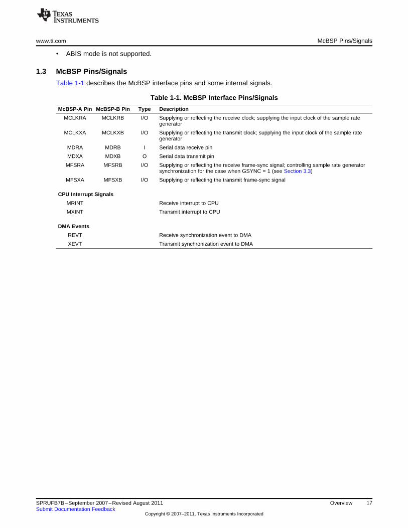
1-1. McBSP Interface Pins/Signals ........................................................................................... 17
2-1. Register Bits That Determine the Number of Phases, Words, and Bits............................................ 25
2-2. Interrupts and DMA Events Generated by a McBSP ................................................................. 30
3-1. Effects of DLB and CLKSTP on Clock Modes......................................................................... 33
3-2. Choosing an Input Clock for the Sample Rate Generator with the SCLKME and CLKSM Bits................. 33
3-3. Polarity Options for the Input to the Sample Rate Generator ....................................................... 34
3-4. Input Clock Selection for Sample Rate Generator .................................................................... 37
5-1. Block - Channel Assignment ............................................................................................. 50
5-2. 2-Partition Mode ........................................................................................................... 50
5-3. 8-Partition mode ........................................................................................................... 50
5-4. Receive Channel Assignment and Control With Eight Receive Partitions ......................................... 53
5-5. Transmit Channel Assignment and Control When Eight Transmit Partitions Are Used.......................... 54
5-6. Selecting a Transmit Multichannel Selection Mode With the XMCM Bits.......................................... 55
6-1. Bits Used to Enable and Configure the Clock Stop Mode ........................................................... 61
6-2. Effects of CLKSTP, CLKXP, and CLKRP on the Clock Scheme ................................................... 61
6-3. Bit Values Required to Configure the McBSP as an SPI Master ................................................... 64
6-4. Bit Values Required to Configure the McBSP as an SPI Slave ..................................................... 65
7-1. Register Bits Used to Reset or Enable the McBSP Receiver Field Descriptions ................................. 68
7-2. Reset State of Each McBSP Pin ........................................................................................ 69
7-3. Register Bit Used to Enable/Disable the Digital Loopback Mode ................................................... 69
7-4. Receive Signals Connected to Transmit Signals in Digital Loopback Mode ...................................... 70
7-5. Register Bits Used to Enable/Disable the Clock Stop Mode ........................................................ 70
7-6. Effects of CLKSTP, CLKXP, and CLKRP on the Clock Scheme ................................................... 71
7-7. Register Bit Used to Enable/Disable the Receive Multichannel Selection Mode ................................. 71
7-8. Register Bit Used to Choose One or Two Phases for the Receive Frame ........................................ 71
7-9. Register Bits Used to Set the Receive Word Length(s) .............................................................. 72
7-10. Register Bits Used to Set the Receive Frame Length................................................................ 72
7-11. How to Calculate the Length of the Receive Frame .................................................................. 73
7-12. Register Bit Used to Enable/Disable the Receive Frame-Synchronization Ignore Function .................... 73
7-13. Register Bits Used to Set the Receive Companding Mode .......................................................... 74
7-14. Register Bits Used to Set the Receive Data Delay ................................................................... 75
7-15. Register Bits Used to Set the Receive Sign-Extension and Justification Mode................................... 77
7-16. Example: Use of RJUST Field With 12-Bit Data Value ABCh....................................................... 77
7-17. Example: Use of RJUST Field With 20-Bit Data Value ABCDEh ................................................... 77
7-18. Register Bits Used to Set the Receive Interrupt Mode ............................................................... 79
7-19. Register Bits Used to Set the Receive Frame Synchronization Mode ............................................ 79
7-20. Select Sources to Provide the Receive Frame-Synchronization Signal and the Effect on the FSR Pin....... 80
7-21. Register Bit Used to Set Receive Frame-Synchronization Polarity ................................................. 81
7-22. Register Bits Used to Set the SRG Frame-Synchronization Period and Pulse Width ........................... 82
7-23. Register Bits Used to Set the Receive Clock Mode .................................................................. 83
7-24. Receive Clock Signal Source Selection ................................................................................ 84
7-25. Register Bit Used to Set Receive Clock Polarity ...................................................................... 84
7-26. Register Bits Used to Set the Sample Rate Generator (SRG) Clock Divide-Down Value....................... 86
7-27. Register Bit Used to Set the SRG Clock Synchronization Mode.................................................... 86
7-28. Register Bits Used to Set the SRG Clock Mode (Choose an Input Clock) ........................................ 86
7-29. Register Bits Used to Set the SRG Input Clock Polarity ............................................................. 88
8-1. Register Bits Used to Place Transmitter in Reset Field Descriptions .............................................. 90
10 List of Tables SPRUFB7B–September 2007–Revised August 2011Submit Documentation Feedback
Copyright © 2007–2011, Texas Instruments Incorporated
www.ti.com
8-2. Register Bit Used to Enable/Disable the Digital Loopback Mode ................................................... 91
8-3. Receive Signals Connected to Transmit Signals in Digital Loopback Mode ...................................... 91
8-4. Register Bits Used to Enable/Disable the Clock Stop Mode ........................................................ 92
8-5. Effects of CLKSTP, CLKXP, and CLKRP on the Clock Scheme ................................................... 92
8-6. Register Bits Used to Enable/Disable Transmit Multichannel Selection ........................................... 93
8-7. Register Bit Used to Choose 1 or 2 Phases for the Transmit Frame............................................... 94
8-8. Register Bits Used to Set the Transmit Word Length(s) ............................................................. 94
8-9. Register Bits Used to Set the Transmit Frame Length ............................................................... 95
8-10. How to Calculate Frame Length......................................................................................... 95
8-11. Register Bit Used to Enable/Disable the Transmit Frame-Synchronization Ignore Function.................... 96
8-12. Register Bits Used to Set the Transmit Companding Mode ......................................................... 97
8-13. Register Bits Used to Set the Transmit Data Delay................................................................... 98
8-14. Register Bit Used to Set the Transmit DXENA (DX Delay Enabler) Mode....................................... 100
8-15. Register Bits Used to Set the Transmit Interrupt Mode ............................................................. 100
8-16. Register Bits Used to Set the Transmit Frame-Synchronization Mode ........................................... 101
8-17. How FSXM and FSGM Select the Source of Transmit Frame-Synchronization Pulses........................ 101
8-18. Register Bit Used to Set Transmit Frame-Synchronization Polarity............................................... 102
8-19. Register Bits Used to Set SRG Frame-Synchronization Period and Pulse Width............................... 103
8-20. Register Bit Used to Set the Transmit Clock Mode ................................................................. 104
8-21. How the CLKXM Bit Selects the Transmit Clock and the Corresponding Status of the MCLKX pin ......... 104
8-22. Register Bit Used to Set Transmit Clock Polarity.................................................................... 104
9-1. McBSP Emulation Modes Selectable with FREE and SOFT Bits of SPCR2 .................................... 108
9-2. Reset State of Each McBSP Pin....................................................................................... 108
11-1. McBSP Register Summary ............................................................................................. 116
11-2. Serial Port Control 1 Register (SPCR1) Field Descriptions ....................................................... 119
11-3. Serial Port Control 2 Register (SPCR2) Field Descriptions ........................................................ 121
11-4. Receive Control Register 1 (RCR1) Field Descriptions............................................................. 123
11-5. Frame Length Formula for Receive Control 1 Register (RCR1)................................................... 124
11-6. Receive Control Register 2 (RCR2) Field Descriptions............................................................. 124
11-7. Frame Length Formula for Receive Control 2 Register (RCR2)................................................... 125
11-8. Transmit Control 1 Register (XCR1) Field Descriptions ........................................................... 126
11-9. Frame Length Formula for Transmit Control 1 Register (XCR1) .................................................. 126
11-10. Transmit Control 2 Register (XCR2) Field Descriptions ............................................................ 127
11-11. Frame Length Formula for Transmit Control 2 Register (XCR2) .................................................. 128
11-12. Sample Rate Generator 1 Register (SRGR1) Field Descriptions ................................................. 129
11-13. Sample Rate Generator 2 Register (SRGR2) Field Descriptions ................................................. 130
11-14. Multichannel Control 1 Register (MCR1) Field Descriptions ....................................................... 131
11-15. Multichannel Control 2 Register (MCR2) Field Descriptions ....................................................... 133
11-16. Pin Control Register (PCR) Field Descriptions....................................................................... 135
11-17. Pin Configuration ........................................................................................................ 137
11-18. Receive Channel Enable Registers (RCERA...RCERH) Field Descriptions ..................................... 138
11-19. Use of the Receive Channel Enable Registers ..................................................................... 138
11-20. Transmit Channel Enable Registers (XCERA...XCERH) Field Descriptions..................................... 140
11-21. Use of the Transmit Channel Enable Registers ..................................................................... 140
11-22. Receive Interrupt Sources and Signals ............................................................................... 142
11-23. Transmit Interrupt Sources and Signals .............................................................................. 142
11-24. Error Flags ............................................................................................................... 143
11-25. McBSP Interrupt Enable Register (MFFINT) Field Descriptions................................................... 143
11-26. McBSP Mode Selection ................................................................................................. 144
11SPRUFB7B–September 2007–Revised August 2011 List of TablesSubmit Documentation Feedback
Copyright © 2007–2011, Texas Instruments Incorporated
www.ti.com
A-1. Changes in this Revision................................................................................................ 145
12 List of Tables SPRUFB7B–September 2007–Revised August 2011Submit Documentation Feedback
Copyright © 2007–2011, Texas Instruments Incorporated
PrefaceSPRUFB7B–September 2007–Revised August 2011
Read This First
About This Manual
This document describes the multichannel buffered serial port (McBSP) of the 28x device. There are up totwo McBSPs on the 2833x/2823x device.
Notational Conventions
This document uses the following conventions.
• Hexadecimal numbers are shown with the suffix h. For example, the following number is 40hexadecimal (decimal 64): 40h.
Related Documentation From Texas Instruments
The following documents describe the 28xxx device and related peripherals. Copies of these documentsare available by contacting your TI representative.
Data Manual and Errata—SPRS439— TMS320F28335, TMS320F28334, TMS320F28332, TMS320F28235, TMS320F28234,
TMS320F28232 Digital Signal Controllers (DSCs) Data Manual contains the pinout, signaldescriptions, as well as electrical and timing specifications for the F2833x/2823x devices.
SPRZ272— TMS320F28335, F28334, F28332, TMS320F28235, F28234, F28232 Digital SignalControllers (DSCs) Silicon Errata describes the advisories and usage notes for different versions ofsilicon.
CPU User's Guides—SPRU430 — TMS320C28x CPU and Instruction Set Reference Guide describes the central processing
unit (CPU) and the assembly language instructions of the TMS320C28x fixed-point digital signalprocessors (DSPs). It also describes emulation features available on these DSPs.
SPRUEO2 — TMS320C28x Floating Point Unit and Instruction Set Reference Guide describes thefloating-point unit and includes the instructions for the FPU.
Peripheral Guides—
SPRU566 — TMS320x28xx, 28xxx DSP Peripheral Reference Guide describes the peripheralreference guides of the 28x digital signal processors (DSPs).
SPRUFB0 — TMS320x2833x, 2823x System Control and Interrupts Reference Guide describes thevarious interrupts and system control features of the 2833x and 2823x digital signal controllers(DSCs).
SPRU812 — TMS320x2833x, 2823x Analog-to-Digital Converter (ADC) Reference Guide describeshow to configure and use the on-chip ADC module, which is a 12-bit pipelined ADC.
SPRU949 — TMS320x2833x, 2823x DSC External Interface (XINTF) Reference Guide describes theXINTF, which is a nonmultiplexed asynchronous bus, as it is used on the 2833x and 2823x devices.
SPRU963 — TMS320x2833x, 2823x Boot ROM Reference Guide describes the purpose and features ofthe bootloader (factory-programmed boot-loading software) and provides examples of code. It alsodescribes other contents of the device on-chip boot ROM and identifies where all of the informationis located within that memory.
13SPRUFB7B–September 2007–Revised August 2011 Read This FirstSubmit Documentation Feedback
Copyright © 2007–2011, Texas Instruments Incorporated
Related Documentation From Texas Instruments www.ti.com
SPRUFB7 — TMS320x2833x, 2823x Multichannel Buffered Serial Port (McBSP) Reference Guidedescribes the McBSP available on the 2833x and 2823x devices. The McBSPs allow directinterface between a DSP and other devices in a system.
SPRUFB8 — TMS320x2833x, 2823x Direct Memory Access (DMA) Module Reference Guidedescribes the DMA on the 2833x and 2823x devices.
SPRUG04 — TMS320x2833x, 2823x Enhanced Pulse Width Modulator (ePWM) Module ReferenceGuide describes the main areas of the enhanced pulse width modulator that include digital motorcontrol, switch mode power supply control, UPS (uninterruptible power supplies), and other forms ofpower conversion.
SPRUG02 — TMS320x2833x, 2823x High-Resolution Pulse Width Modulator (HRPWM) ReferenceGuide describes the operation of the high-resolution extension to the pulse width modulator(HRPWM).
SPRUFG4 — TMS320x2833x, 2823x Enhanced Capture (eCAP) Module Reference Guide describesthe enhanced capture module. It includes the module description and registers.
SPRUG05 — TMS320x2833x, 2823x Enhanced Quadrature Encoder Pulse (eQEP) ModuleReference Guide describes the eQEP module, which is used for interfacing with a linear or rotaryincremental encoder to get position, direction, and speed information from a rotating machine inhigh-performance motion and position control systems. It includes the module description andregisters.
SPRUEU1 — TMS320x2833x, 2823x Enhanced Controller Area Network (eCAN) Reference Guidedescribes the eCAN that uses established protocol to communicate serially with other controllers inelectrically noisy environments.
SPRUFZ5 — TMS320x2833x, 2823x Serial Communications Interface (SCI) Reference Guidedescribes the SCI, which is a two-wire asynchronous serial port, commonly known as a UART. TheSCI modules support digital communications between the CPU and other asynchronous peripheralsthat use the standard non-return-to-zero (NRZ) format.
SPRUEU3 — TMS320x2833x, 2823x DSC Serial Peripheral Interface (SPI) Reference Guidedescribes the SPI - a high-speed synchronous serial input/output (I/O) port - that allows a serial bitstream of programmed length (one to sixteen bits) to be shifted into and out of the device at aprogrammed bit-transfer rate.
SPRUG03 — TMS320x2833x, 2823x Inter-Integrated Circuit (I2C) Module Reference Guide describesthe features and operation of the inter-integrated circuit (I2C) module.
Tools Guides—SPRU513 — TMS320C28x Assembly Language Tools v5.0.0 User's Guide describes the assembly
language tools (assembler and other tools used to develop assembly language code), assemblerdirectives, macros, common object file format, and symbolic debugging directives for theTMS320C28x device.
SPRU514 — TMS320C28x Optimizing C/C++ Compiler v5.0.0 User's Guide describes theTMS320C28x™ C/C++ compiler. This compiler accepts ANSI standard C/C++ source code andproduces TMS320 DSP assembly language source code for the TMS320C28x device.
SPRU608 — TMS320C28x Instruction Set Simulator Technical Overview describes the simulator,available within the Code Composer Studio for TMS320C2000 IDE, that simulates the instructionset of the C28x™ core.
SPRU625 — TMS320C28x DSP/BIOS 5.32 Application Programming Interface (API) ReferenceGuide describes development using DSP/BIOS.
TMS320C28x, C28x are trademarks of Texas Instruments.
14 Read This First SPRUFB7B–September 2007–Revised August 2011Submit Documentation Feedback
Copyright © 2007–2011, Texas Instruments Incorporated
Chapter 1SPRUFB7B–September 2007–Revised August 2011
Overview
This document describes the multichannel buffered serial port (McBSP) of the 2833x/2823x device.
Topic ........................................................................................................................... Page
1.1 Brief Description ............................................................................................... 161.2 Features of the McBSPs ..................................................................................... 161.3 McBSP Pins/Signals .......................................................................................... 17
15SPRUFB7B–September 2007–Revised August 2011 OverviewSubmit Documentation Feedback
Copyright © 2007–2011, Texas Instruments Incorporated
Brief Description www.ti.com
1.1 Brief Description
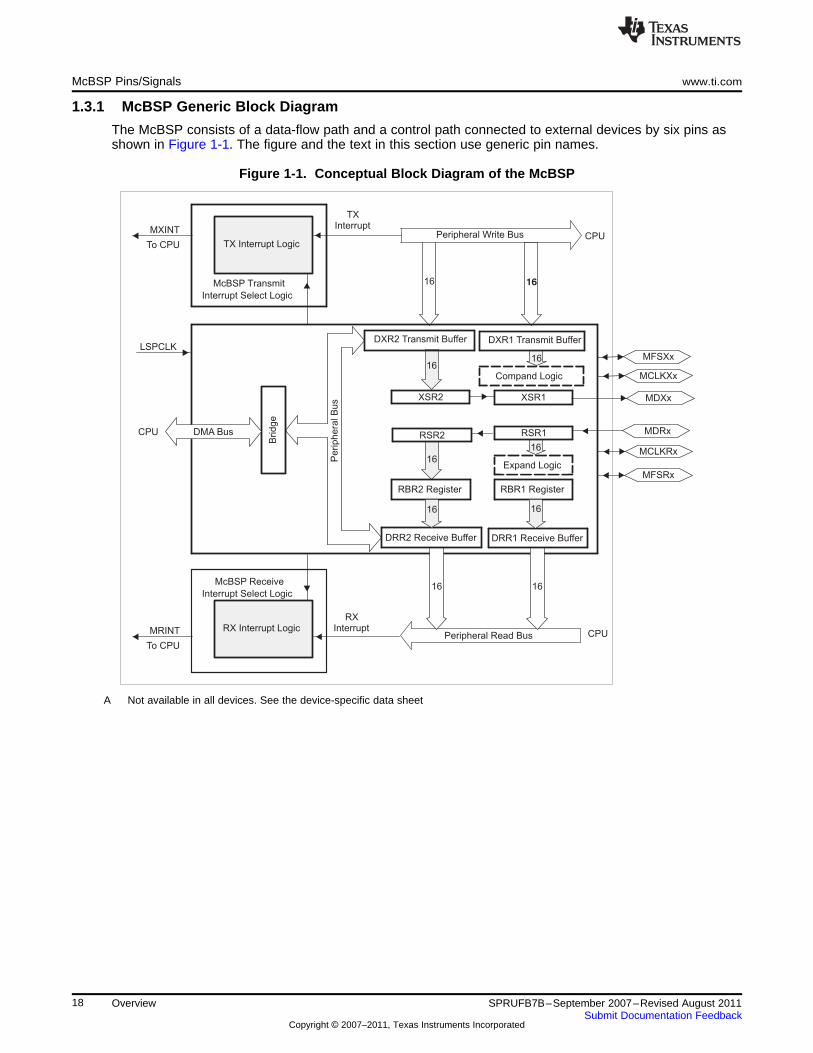
This device provides up to two high-speed multichannel buffered serial ports (McBSPs) that allow directinterface to codecs and other devices in a system. The McBSP consists of a data-flow path and a controlpath connected to external devices by six pins as shown in Figure 1-1.
Data is communicated to devices interfaced with the McBSP via the data transmit (DX) pin fortransmission and via the data receive (DR) pin for reception. Control information in the form of clockingand frame synchronization is communicated via the following pins: CLKX (transmit clock), CLKR (receiveclock), FSX (transmit frame synchronization), and FSR (receive frame synchronization).
The CPU and the DMA controller communicate with the McBSP through 16-bit-wide registers accessiblevia the internal peripheral bus. The CPU or the DMA controller writes the data to be transmitted to thedata transmit registers (DXR1, DXR2). Data written to the DXRs is shifted out to DX via the transmit shiftregisters (XSR1, XSR2). Similarly, receive data on the DR pin is shifted into the receive shift registers(RSR1, RSR2) and copied into the receive buffer registers (RBR1, RBR2). The contents of the RBRs isthen copied to the DRRs, which can be read by the CPU or the DMA controller. This allows simultaneousmovement of internal and external data communications.
DRR2, RBR2, RSR2, DXR2, and XSR2 are not used (written, read, or shifted) if the serial word length is 8bits, 12 bits, or 16 bits. For larger word lengths, these registers are needed to hold the most significantbits.
The frame and clock loop-back is implemented at chip level to enable CLKX and FSX to drive CLKR andFSR. If the loop-back is enabled, the CLKR and FSR get their signals from the CLKX and FSX pads;instead of the CLKR and FSR pins.
1.2 Features of the McBSPs
The McBSPs feature:
• Full-duplex communication
• Double-buffered transmission and triple-buffered reception, allowing a continuous data stream
• Independent clocking and framing for reception and transmission
• The capability to send interrupts to the CPU and to send DMA events to the DMA controller
• 128 channels for transmission and reception
• Multichannel selection modes that enable or disable block transfers in each of the channels
• Direct interface to industry-standard codecs, analog interface chips (AICs), and other seriallyconnected A/D and D/A devices
• Support for external generation of clock signals and frame-synchronization signals
• A programmable sample rate generator for internal generation and control of clock signals andframe-synchronization signals
• Programmable polarity for frame-synchronization pulses and clock signals
• Direct interface to:
– T1/E1 framers
– IOM-2 compliant devices
– AC97-compliant devices (the necessary multiphase frame capability is provided)
– I2S compliant devices
– SPI devices
• A wide selection of data sizes: 8, 12, 16, 20, 24, and 32 bits
NOTE: A value of the chosen data size is referred to as a serial word or word throughout theMcBSP documentation. Elsewhere, word is used to describe a 16-bit value.
• μ-law and A-law companding
• The option of transmitting/receiving 8-bit data with the LSB first
• Status bits for flagging exception/error conditions
16 Overview SPRUFB7B–September 2007–Revised August 2011Submit Documentation Feedback
Copyright © 2007–2011, Texas Instruments Incorporated
www.ti.com McBSP Pins/Signals
• ABIS mode is not supported.
1.3 McBSP Pins/Signals
Table 1-1 describes the McBSP interface pins and some internal signals.
Table 1-1. McBSP Interface Pins/Signals
McBSP-A Pin McBSP-B Pin Type Description
MCLKRA MCLKRB I/O Supplying or reflecting the receive clock; supplying the input clock of the sample rategenerator
MCLKXA MCLKXB I/O Supplying or reflecting the transmit clock; supplying the input clock of the sample rategenerator
MDRA MDRB I Serial data receive pin
MDXA MDXB O Serial data transmit pin
MFSRA MFSRB I/O Supplying or reflecting the receive frame-sync signal; controlling sample rate generatorsynchronization for the case when GSYNC = 1 (see Section 3.3)
MFSXA MFSXB I/O Supplying or reflecting the transmit frame-sync signal
CPU Interrupt Signals
MRINT Receive interrupt to CPU
MXINT Transmit interrupt to CPU
DMA Events
REVT Receive synchronization event to DMA
XEVT Transmit synchronization event to DMA
17SPRUFB7B–September 2007–Revised August 2011 OverviewSubmit Documentation Feedback
Copyright © 2007–2011, Texas Instruments Incorporated
16
McBSP Receive
Interrupt Select Logic
MDXx
MDRx
Expand Logic
DRR1 Receive Buffer
RXInterrupt
DRR2 Receive Buffer
RBR1 RegisterRBR2 Register
MCLKXx
MFSXx
MCLKRx
MFSRx
16
Compand Logic
DXR2 Transmit Buffer
RSR1
XSR2 XSR1
Peripheral Read Bus
16
1616
1616
RSR2
DXR1 Transmit BufferLSPCLK
MRINT
To CPU
RX Interrupt Logic
McBSP Transmit
Interrupt Select Logic
TXInterruptMXINT
To CPU TX Interrupt Logic
16
16 16
Brid
ge
DMA Bus
Pe
rip
he
ral B
us
Peripheral Write Bus
CPU
CPU
CPU
McBSP Pins/Signals www.ti.com
1.3.1 McBSP Generic Block Diagram
The McBSP consists of a data-flow path and a control path connected to external devices by six pins asshown in Figure 1-1. The figure and the text in this section use generic pin names.
Figure 1-1. Conceptual Block Diagram of the McBSP
A Not available in all devices. See the device-specific data sheet
18 Overview SPRUFB7B–September 2007–Revised August 2011Submit Documentation Feedback
Copyright © 2007–2011, Texas Instruments Incorporated
Chapter 2SPRUFB7B–September 2007–Revised August 2011
McBSP Operation
This section addresses the following topics:
• Data transfer process
• Companding (compressing and expanding) data
• Clocking and framing data
• Frame phases
• McBSP reception
• McBSP transmission
• Interrupts and DMA events generated by McBSPs
Topic ........................................................................................................................... Page
2.1 Data Transfer Process of McBSPs ....................................................................... 202.2 Companding (Compressing and Expanding) Data ................................................. 202.3 Clocking and Framing Data ................................................................................ 222.4 Frame Phases ................................................................................................... 242.5 McBSP Reception .............................................................................................. 262.6 McBSP Transmission ......................................................................................... 292.7 Interrupts and DMA Events Generated by a McBSP ............................................... 30
19SPRUFB7B–September 2007–Revised August 2011 McBSP OperationSubmit Documentation Feedback
Copyright © 2007–2011, Texas Instruments Incorporated
ÁÁÁÁÁÁÁÁÁÁÁÁÁÁÁÁÁÁÁÁÁÁÁÁÁÁÁÁÁÁÁÁÁÁÁÁÁÁÁÁÁÁÁÁÁÁÁÁDX
DR
Compand
RSR[1,2]
Compress
Expand
XSR[1,2]
ÁÁÁÁÁÁÁÁÁÁÁÁÁÁÁÁRBR[1,2] DRR[1,2]ÁÁÁÁÁÁÁÁÁÁÁÁÁÁÁÁDXR[1,2]
DRR[1,2]RBR[1,2] To CPU/DMA controller
From CPU/DMA controller
Data Transfer Process of McBSPs www.ti.com
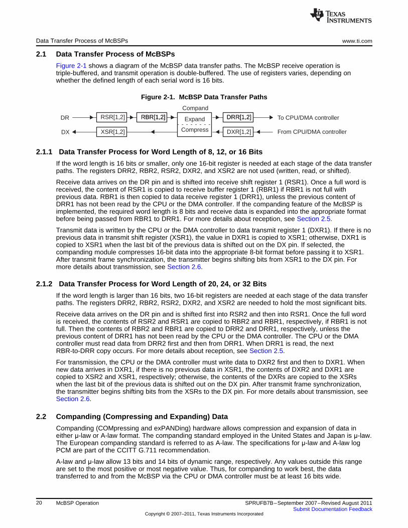
2.1 Data Transfer Process of McBSPs
Figure 2-1 shows a diagram of the McBSP data transfer paths. The McBSP receive operation istriple-buffered, and transmit operation is double-buffered. The use of registers varies, depending onwhether the defined length of each serial word is 16 bits.
Figure 2-1. McBSP Data Transfer Paths
2.1.1 Data Transfer Process for Word Length of 8, 12, or 16 Bits
If the word length is 16 bits or smaller, only one 16-bit register is needed at each stage of the data transferpaths. The registers DRR2, RBR2, RSR2, DXR2, and XSR2 are not used (written, read, or shifted).
Receive data arrives on the DR pin and is shifted into receive shift register 1 (RSR1). Once a full word isreceived, the content of RSR1 is copied to receive buffer register 1 (RBR1) if RBR1 is not full withprevious data. RBR1 is then copied to data receive register 1 (DRR1), unless the previous content ofDRR1 has not been read by the CPU or the DMA controller. If the companding feature of the McBSP isimplemented, the required word length is 8 bits and receive data is expanded into the appropriate formatbefore being passed from RBR1 to DRR1. For more details about reception, see Section 2.5.
Transmit data is written by the CPU or the DMA controller to data transmit register 1 (DXR1). If there is noprevious data in transmit shift register (XSR1), the value in DXR1 is copied to XSR1; otherwise, DXR1 iscopied to XSR1 when the last bit of the previous data is shifted out on the DX pin. If selected, thecompanding module compresses 16-bit data into the appropriate 8-bit format before passing it to XSR1.After transmit frame synchronization, the transmitter begins shifting bits from XSR1 to the DX pin. Formore details about transmission, see Section 2.6.
2.1.2 Data Transfer Process for Word Length of 20, 24, or 32 Bits
If the word length is larger than 16 bits, two 16-bit registers are needed at each stage of the data transferpaths. The registers DRR2, RBR2, RSR2, DXR2, and XSR2 are needed to hold the most significant bits.
Receive data arrives on the DR pin and is shifted first into RSR2 and then into RSR1. Once the full wordis received, the contents of RSR2 and RSR1 are copied to RBR2 and RBR1, respectively, if RBR1 is notfull. Then the contents of RBR2 and RBR1 are copied to DRR2 and DRR1, respectively, unless theprevious content of DRR1 has not been read by the CPU or the DMA controller. The CPU or the DMAcontroller must read data from DRR2 first and then from DRR1. When DRR1 is read, the nextRBR-to-DRR copy occurs. For more details about reception, see Section 2.5.
For transmission, the CPU or the DMA controller must write data to DXR2 first and then to DXR1. Whennew data arrives in DXR1, if there is no previous data in XSR1, the contents of DXR2 and DXR1 arecopied to XSR2 and XSR1, respectively; otherwise, the contents of the DXRs are copied to the XSRswhen the last bit of the previous data is shifted out on the DX pin. After transmit frame synchronization,the transmitter begins shifting bits from the XSRs to the DX pin. For more details about transmission, seeSection 2.6.
2.2 Companding (Compressing and Expanding) Data
Companding (COMpressing and exPANDing) hardware allows compression and expansion of data ineither μ-law or A-law format. The companding standard employed in the United States and Japan is μ-law.The European companding standard is referred to as A-law. The specifications for μ-law and A-law logPCM are part of the CCITT G.711 recommendation.
A-law and μ-law allow 13 bits and 14 bits of dynamic range, respectively. Any values outside this rangeare set to the most positive or most negative value. Thus, for companding to work best, the datatransferred to and from the McBSP via the CPU or DMA controller must be at least 16 bits wide.
20 McBSP Operation SPRUFB7B–September 2007–Revised August 2011Submit Documentation Feedback
Copyright © 2007–2011, Texas Instruments Incorporated
From CPU or DMA controllerDXR1
To CPU or DMA controllerDRR1
16
16
DX8
8
XSR1 Compress
ExpandDR RBR1RSR1
µ-law format in DXR1 00Value
1-015-2
000
2-0
Value
15-3
A-law format in DXR1
www.ti.com Companding (Compressing and Expanding) Data
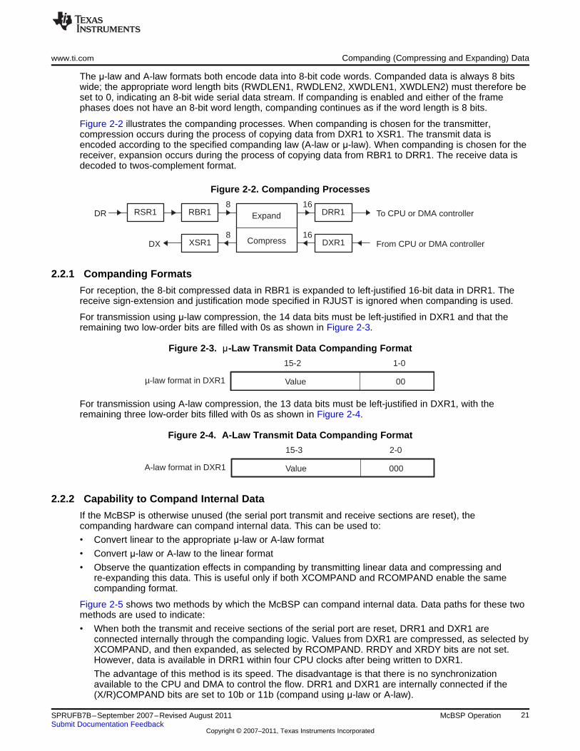
The μ-law and A-law formats both encode data into 8-bit code words. Companded data is always 8 bitswide; the appropriate word length bits (RWDLEN1, RWDLEN2, XWDLEN1, XWDLEN2) must therefore beset to 0, indicating an 8-bit wide serial data stream. If companding is enabled and either of the framephases does not have an 8-bit word length, companding continues as if the word length is 8 bits.
Figure 2-2 illustrates the companding processes. When companding is chosen for the transmitter,compression occurs during the process of copying data from DXR1 to XSR1. The transmit data isencoded according to the specified companding law (A-law or μ-law). When companding is chosen for thereceiver, expansion occurs during the process of copying data from RBR1 to DRR1. The receive data isdecoded to twos-complement format.
Figure 2-2. Companding Processes
2.2.1 Companding Formats
For reception, the 8-bit compressed data in RBR1 is expanded to left-justified 16-bit data in DRR1. Thereceive sign-extension and justification mode specified in RJUST is ignored when companding is used.
For transmission using μ-law compression, the 14 data bits must be left-justified in DXR1 and that theremaining two low-order bits are filled with 0s as shown in Figure 2-3.
Figure 2-3. μ-Law Transmit Data Companding Format
For transmission using A-law compression, the 13 data bits must be left-justified in DXR1, with theremaining three low-order bits filled with 0s as shown in Figure 2-4.
Figure 2-4. A-Law Transmit Data Companding Format
2.2.2 Capability to Compand Internal Data
If the McBSP is otherwise unused (the serial port transmit and receive sections are reset), thecompanding hardware can compand internal data. This can be used to:
• Convert linear to the appropriate μ-law or A-law format
• Convert μ-law or A-law to the linear format
• Observe the quantization effects in companding by transmitting linear data and compressing andre-expanding this data. This is useful only if both XCOMPAND and RCOMPAND enable the samecompanding format.
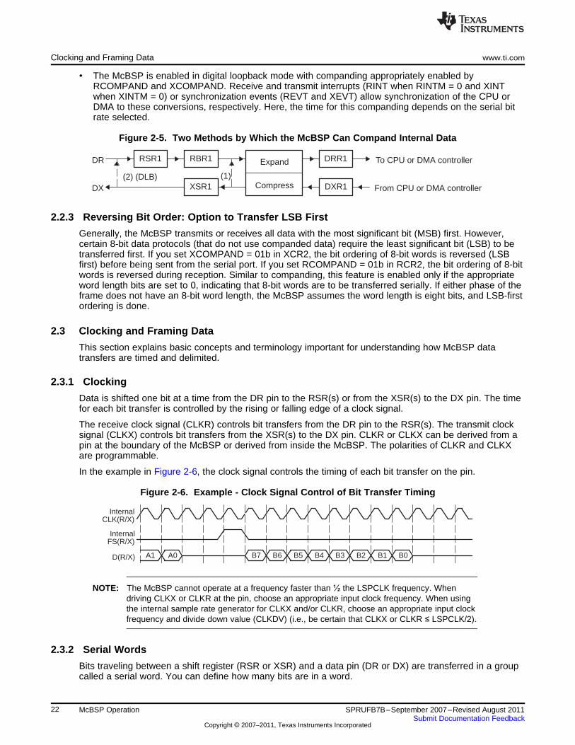
Figure 2-5 shows two methods by which the McBSP can compand internal data. Data paths for these twomethods are used to indicate:
• When both the transmit and receive sections of the serial port are reset, DRR1 and DXR1 areconnected internally through the companding logic. Values from DXR1 are compressed, as selected byXCOMPAND, and then expanded, as selected by RCOMPAND. RRDY and XRDY bits are not set.However, data is available in DRR1 within four CPU clocks after being written to DXR1.
The advantage of this method is its speed. The disadvantage is that there is no synchronizationavailable to the CPU and DMA to control the flow. DRR1 and DXR1 are internally connected if the(X/R)COMPAND bits are set to 10b or 11b (compand using μ-law or A-law).
21SPRUFB7B–September 2007–Revised August 2011 McBSP OperationSubmit Documentation Feedback
Copyright © 2007–2011, Texas Instruments Incorporated
(1)(2) (DLB)From CPU or DMA controllerDXR1
To CPU or DMA controllerDRR1
DX XSR1 Compress
ExpandDR RBR1RSR1
D(R/X)
FS(R/X)
CLK(R/X)
B0B1B2B3B4B5B6B7A0A1
ÁÁÁÁÁÁÁÁÁÁÁÁÁÁÁInternal
Internal
Clocking and Framing Data www.ti.com
• The McBSP is enabled in digital loopback mode with companding appropriately enabled byRCOMPAND and XCOMPAND. Receive and transmit interrupts (RINT when RINTM = 0 and XINTwhen XINTM = 0) or synchronization events (REVT and XEVT) allow synchronization of the CPU orDMA to these conversions, respectively. Here, the time for this companding depends on the serial bitrate selected.
Figure 2-5. Two Methods by Which the McBSP Can Compand Internal Data
2.2.3 Reversing Bit Order: Option to Transfer LSB First
Generally, the McBSP transmits or receives all data with the most significant bit (MSB) first. However,certain 8-bit data protocols (that do not use companded data) require the least significant bit (LSB) to betransferred first. If you set XCOMPAND = 01b in XCR2, the bit ordering of 8-bit words is reversed (LSBfirst) before being sent from the serial port. If you set RCOMPAND = 01b in RCR2, the bit ordering of 8-bitwords is reversed during reception. Similar to companding, this feature is enabled only if the appropriateword length bits are set to 0, indicating that 8-bit words are to be transferred serially. If either phase of theframe does not have an 8-bit word length, the McBSP assumes the word length is eight bits, and LSB-firstordering is done.
2.3 Clocking and Framing Data
This section explains basic concepts and terminology important for understanding how McBSP datatransfers are timed and delimited.
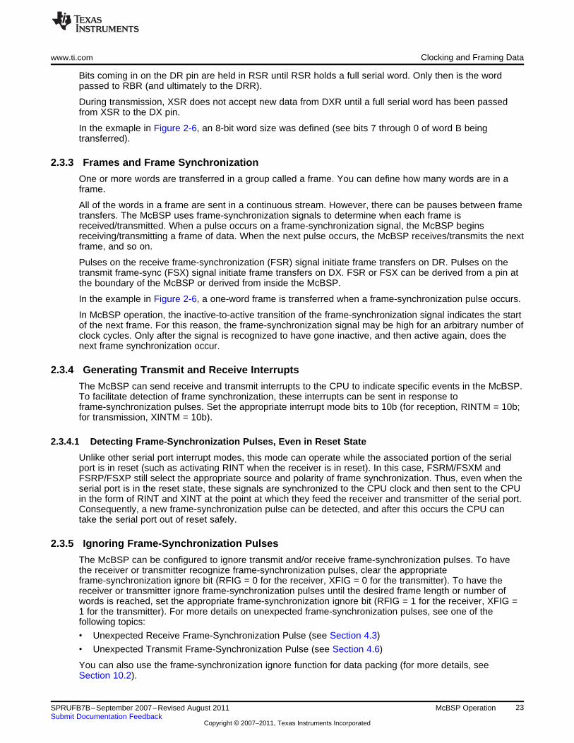
2.3.1 Clocking
Data is shifted one bit at a time from the DR pin to the RSR(s) or from the XSR(s) to the DX pin. The timefor each bit transfer is controlled by the rising or falling edge of a clock signal.
The receive clock signal (CLKR) controls bit transfers from the DR pin to the RSR(s). The transmit clocksignal (CLKX) controls bit transfers from the XSR(s) to the DX pin. CLKR or CLKX can be derived from apin at the boundary of the McBSP or derived from inside the McBSP. The polarities of CLKR and CLKXare programmable.
In the example in Figure 2-6, the clock signal controls the timing of each bit transfer on the pin.
Figure 2-6. Example - Clock Signal Control of Bit Transfer Timing
NOTE: The McBSP cannot operate at a frequency faster than ½ the LSPCLK frequency. Whendriving CLKX or CLKR at the pin, choose an appropriate input clock frequency. When usingthe internal sample rate generator for CLKX and/or CLKR, choose an appropriate input clockfrequency and divide down value (CLKDV) (i.e., be certain that CLKX or CLKR ≤ LSPCLK/2).
2.3.2 Serial Words
Bits traveling between a shift register (RSR or XSR) and a data pin (DR or DX) are transferred in a groupcalled a serial word. You can define how many bits are in a word.
22 McBSP Operation SPRUFB7B–September 2007–Revised August 2011Submit Documentation Feedback
Copyright © 2007–2011, Texas Instruments Incorporated
www.ti.com Clocking and Framing Data
Bits coming in on the DR pin are held in RSR until RSR holds a full serial word. Only then is the wordpassed to RBR (and ultimately to the DRR).
During transmission, XSR does not accept new data from DXR until a full serial word has been passedfrom XSR to the DX pin.
In the exmaple in Figure 2-6, an 8-bit word size was defined (see bits 7 through 0 of word B beingtransferred).
2.3.3 Frames and Frame Synchronization
One or more words are transferred in a group called a frame. You can define how many words are in aframe.
All of the words in a frame are sent in a continuous stream. However, there can be pauses between frametransfers. The McBSP uses frame-synchronization signals to determine when each frame isreceived/transmitted. When a pulse occurs on a frame-synchronization signal, the McBSP beginsreceiving/transmitting a frame of data. When the next pulse occurs, the McBSP receives/transmits the nextframe, and so on.
Pulses on the receive frame-synchronization (FSR) signal initiate frame transfers on DR. Pulses on thetransmit frame-sync (FSX) signal initiate frame transfers on DX. FSR or FSX can be derived from a pin atthe boundary of the McBSP or derived from inside the McBSP.
In the example in Figure 2-6, a one-word frame is transferred when a frame-synchronization pulse occurs.
In McBSP operation, the inactive-to-active transition of the frame-synchronization signal indicates the startof the next frame. For this reason, the frame-synchronization signal may be high for an arbitrary number ofclock cycles. Only after the signal is recognized to have gone inactive, and then active again, does thenext frame synchronization occur.
2.3.4 Generating Transmit and Receive Interrupts
The McBSP can send receive and transmit interrupts to the CPU to indicate specific events in the McBSP.To facilitate detection of frame synchronization, these interrupts can be sent in response toframe-synchronization pulses. Set the appropriate interrupt mode bits to 10b (for reception, RINTM = 10b;for transmission, XINTM = 10b).
2.3.4.1 Detecting Frame-Synchronization Pulses, Even in Reset State
Unlike other serial port interrupt modes, this mode can operate while the associated portion of the serialport is in reset (such as activating RINT when the receiver is in reset). In this case, FSRM/FSXM andFSRP/FSXP still select the appropriate source and polarity of frame synchronization. Thus, even when theserial port is in the reset state, these signals are synchronized to the CPU clock and then sent to the CPUin the form of RINT and XINT at the point at which they feed the receiver and transmitter of the serial port.Consequently, a new frame-synchronization pulse can be detected, and after this occurs the CPU cantake the serial port out of reset safely.
2.3.5 Ignoring Frame-Synchronization Pulses
The McBSP can be configured to ignore transmit and/or receive frame-synchronization pulses. To havethe receiver or transmitter recognize frame-synchronization pulses, clear the appropriateframe-synchronization ignore bit (RFIG = 0 for the receiver, XFIG = 0 for the transmitter). To have thereceiver or transmitter ignore frame-synchronization pulses until the desired frame length or number ofwords is reached, set the appropriate frame-synchronization ignore bit (RFIG = 1 for the receiver, XFIG =1 for the transmitter). For more details on unexpected frame-synchronization pulses, see one of thefollowing topics:
• Unexpected Receive Frame-Synchronization Pulse (see Section 4.3)
• Unexpected Transmit Frame-Synchronization Pulse (see Section 4.6)
You can also use the frame-synchronization ignore function for data packing (for more details, seeSection 10.2).
23SPRUFB7B–September 2007–Revised August 2011 McBSP OperationSubmit Documentation Feedback
Copyright © 2007–2011, Texas Instruments Incorporated
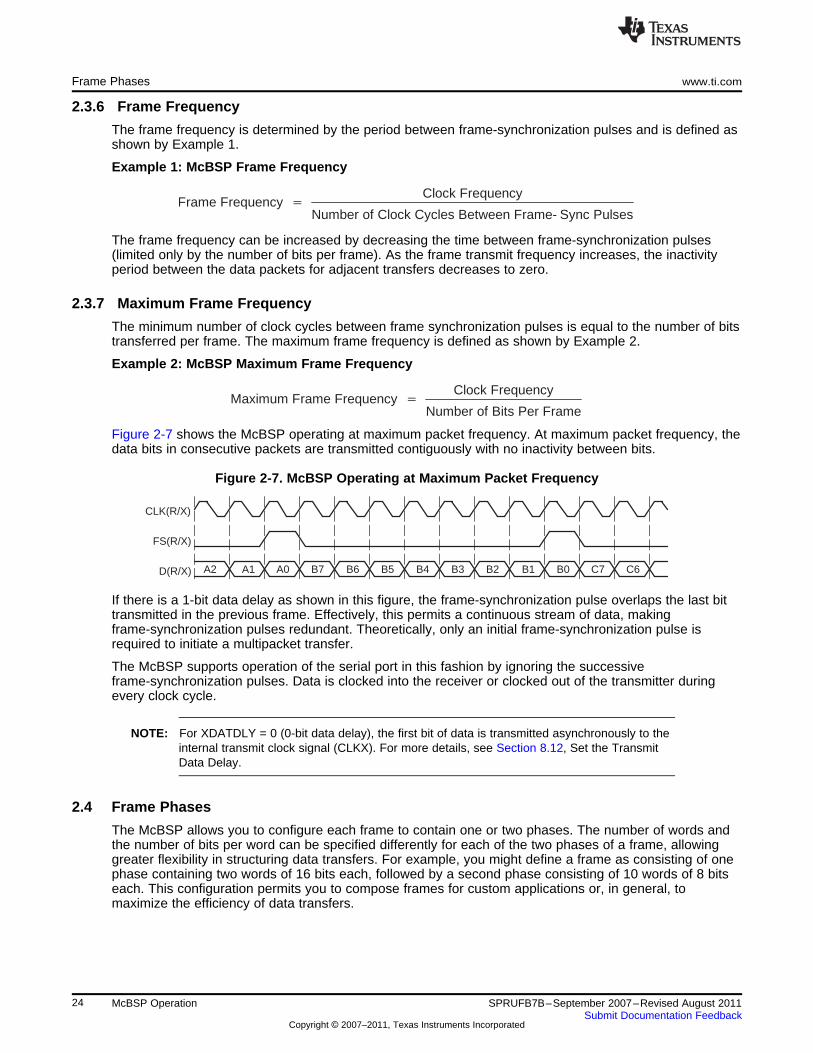
Frame Frequency �
Clock Frequency
Number of Clock Cycles Between Frame- Sync Pulses
Maximum Frame Frequency �
Clock Frequency
Number of Bits Per Frame
D(R/X)
FS(R/X)
CLK(R/X)
C6C7B0B1B2B3B4B5B6B7A0A1A2
Frame Phases www.ti.com
2.3.6 Frame Frequency
The frame frequency is determined by the period between frame-synchronization pulses and is defined asshown by Example 1.
Example 1: McBSP Frame Frequency
The frame frequency can be increased by decreasing the time between frame-synchronization pulses(limited only by the number of bits per frame). As the frame transmit frequency increases, the inactivityperiod between the data packets for adjacent transfers decreases to zero.
2.3.7 Maximum Frame Frequency
The minimum number of clock cycles between frame synchronization pulses is equal to the number of bitstransferred per frame. The maximum frame frequency is defined as shown by Example 2.
Example 2: McBSP Maximum Frame Frequency
Figure 2-7 shows the McBSP operating at maximum packet frequency. At maximum packet frequency, thedata bits in consecutive packets are transmitted contiguously with no inactivity between bits.
Figure 2-7. McBSP Operating at Maximum Packet Frequency
If there is a 1-bit data delay as shown in this figure, the frame-synchronization pulse overlaps the last bittransmitted in the previous frame. Effectively, this permits a continuous stream of data, makingframe-synchronization pulses redundant. Theoretically, only an initial frame-synchronization pulse isrequired to initiate a multipacket transfer.
The McBSP supports operation of the serial port in this fashion by ignoring the successiveframe-synchronization pulses. Data is clocked into the receiver or clocked out of the transmitter duringevery clock cycle.
NOTE: For XDATDLY = 0 (0-bit data delay), the first bit of data is transmitted asynchronously to theinternal transmit clock signal (CLKX). For more details, see Section 8.12, Set the TransmitData Delay.
2.4 Frame Phases
The McBSP allows you to configure each frame to contain one or two phases. The number of words andthe number of bits per word can be specified differently for each of the two phases of a frame, allowinggreater flexibility in structuring data transfers. For example, you might define a frame as consisting of onephase containing two words of 16 bits each, followed by a second phase consisting of 10 words of 8 bitseach. This configuration permits you to compose frames for custom applications or, in general, tomaximize the efficiency of data transfers.
24 McBSP Operation SPRUFB7B–September 2007–Revised August 2011Submit Documentation Feedback
Copyright © 2007–2011, Texas Instruments Incorporated
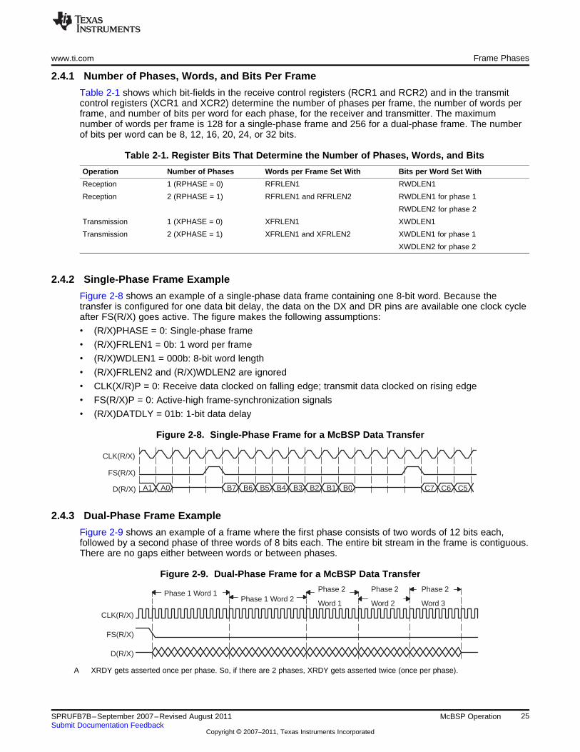
A1D(R/X)
FS(R/X)
CLK(R/X)
C5C6C7B0B1B2B3B4B5B6B7A0
ÁÁÁÁÁÁÁÁÁÁÁÁÁÁÁÁD(R/X)
FS(R/X)
CLK(R/X)
Phase 2
Word 3
Phase 2
Word 2
Phase 2
Word 1 ÁÁÁÁÁÁÁÁÁÁÁÁ ÁÁÁÁÁÁÁÁÁÁÁÁÁÁÁÁÁÁÁÁÁÁÁÁÁÁÁÁÁÁÁÁÁÁÁÁÁÁÁÁÁÁÁÁÁÁÁÁÁÁÁÁÁÁÁÁÁÁÁÁÁÁÁÁÁÁÁÁÁÁÁÁÁÁÁÁÁÁÁÁÁÁÁÁÁÁÁÁÁÁÁÁÁÁÁÁÁÁÁÁÁÁÁÁÁÁÁÁÁÁÁÁÁÁÁÁ ÁÁÁÁ ÁÁÁÁÁÁÁÁÁÁÁÁÁÁÁÁÁÁÁÁÁÁÁÁÁÁÁÁÁÁÁÁÁÁÁÁÁÁÁÁÁÁÁÁÁÁÁÁÁÁÁÁÁÁÁÁÁÁÁÁÁÁÁÁÁÁÁÁÁÁÁÁÁÁÁÁÁÁÁÁÁÁÁÁÁÁÁÁ ÁÁÁÁÁÁÁÁÁÁÁÁÁÁÁÁÁÁÁÁÁÁÁÁÁÁÁÁÁÁÁÁÁÁÁÁÁÁÁÁÁÁÁÁÁÁÁÁÁÁÁÁÁÁÁÁÁÁÁÁÁÁÁÁÁÁÁÁÁÁÁÁÁÁÁÁÁÁÁÁÁÁÁÁÁÁÁÁÁÁÁÁ Phase 1 Word 1Phase 1 Word 2
www.ti.com Frame Phases
2.4.1 Number of Phases, Words, and Bits Per Frame
Table 2-1 shows which bit-fields in the receive control registers (RCR1 and RCR2) and in the transmitcontrol registers (XCR1 and XCR2) determine the number of phases per frame, the number of words perframe, and number of bits per word for each phase, for the receiver and transmitter. The maximumnumber of words per frame is 128 for a single-phase frame and 256 for a dual-phase frame. The numberof bits per word can be 8, 12, 16, 20, 24, or 32 bits.
Table 2-1. Register Bits That Determine the Number of Phases, Words, and Bits
Operation Number of Phases Words per Frame Set With Bits per Word Set With
Reception 1 (RPHASE = 0) RFRLEN1 RWDLEN1
Reception 2 (RPHASE = 1) RFRLEN1 and RFRLEN2 RWDLEN1 for phase 1
RWDLEN2 for phase 2
Transmission 1 (XPHASE = 0) XFRLEN1 XWDLEN1
Transmission 2 (XPHASE = 1) XFRLEN1 and XFRLEN2 XWDLEN1 for phase 1
XWDLEN2 for phase 2
2.4.2 Single-Phase Frame Example
Figure 2-8 shows an example of a single-phase data frame containing one 8-bit word. Because thetransfer is configured for one data bit delay, the data on the DX and DR pins are available one clock cycleafter FS(R/X) goes active. The figure makes the following assumptions:
• (R/X)PHASE = 0: Single-phase frame
• (R/X)FRLEN1 = 0b: 1 word per frame
• (R/X)WDLEN1 = 000b: 8-bit word length
• (R/X)FRLEN2 and (R/X)WDLEN2 are ignored
• CLK(X/R)P = 0: Receive data clocked on falling edge; transmit data clocked on rising edge
• FS(R/X)P = 0: Active-high frame-synchronization signals
• (R/X)DATDLY = 01b: 1-bit data delay
Figure 2-8. Single-Phase Frame for a McBSP Data Transfer
2.4.3 Dual-Phase Frame Example
Figure 2-9 shows an example of a frame where the first phase consists of two words of 12 bits each,followed by a second phase of three words of 8 bits each. The entire bit stream in the frame is contiguous.There are no gaps either between words or between phases.
Figure 2-9. Dual-Phase Frame for a McBSP Data Transfer
A XRDY gets asserted once per phase. So, if there are 2 phases, XRDY gets asserted twice (once per phase).
25SPRUFB7B–September 2007–Revised August 2011 McBSP OperationSubmit Documentation Feedback
Copyright © 2007–2011, Texas Instruments Incorporated
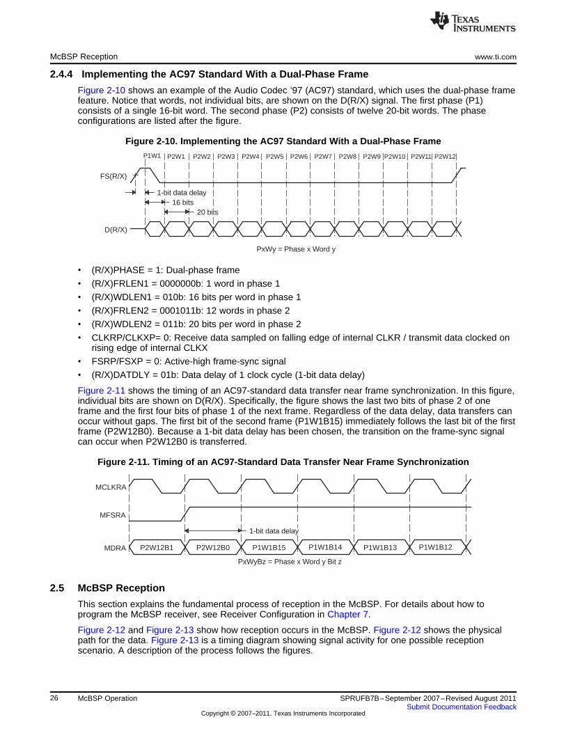
PxWy = Phase x Word y
D(R/X)
FS(R/X)
P2W12P2W11P2W10P2W9P2W8P2W7P2W6P2W5P2W4P2W3P2W2P2W1P1W1ÁÁÁÁÁÁÁÁ 20 bits16 bits
1-bit data delay
PxWyBz = Phase x Word y Bit z
ÁÁÁÁ P2W12B0P2W12B1MDRA P1W1B15 P1W1B12P1W1B13P1W1B14
MFSRA
MCLKRA
1-bit data delay
McBSP Reception www.ti.com
2.4.4 Implementing the AC97 Standard With a Dual-Phase Frame
Figure 2-10 shows an example of the Audio Codec ‘97 (AC97) standard, which uses the dual-phase framefeature. Notice that words, not individual bits, are shown on the D(R/X) signal. The first phase (P1)consists of a single 16-bit word. The second phase (P2) consists of twelve 20-bit words. The phaseconfigurations are listed after the figure.
Figure 2-10. Implementing the AC97 Standard With a Dual-Phase Frame
• (R/X)PHASE = 1: Dual-phase frame
• (R/X)FRLEN1 = 0000000b: 1 word in phase 1
• (R/X)WDLEN1 = 010b: 16 bits per word in phase 1
• (R/X)FRLEN2 = 0001011b: 12 words in phase 2
• (R/X)WDLEN2 = 011b: 20 bits per word in phase 2
• CLKRP/CLKXP= 0: Receive data sampled on falling edge of internal CLKR / transmit data clocked onrising edge of internal CLKX
• FSRP/FSXP = 0: Active-high frame-sync signal
• (R/X)DATDLY = 01b: Data delay of 1 clock cycle (1-bit data delay)
Figure 2-11 shows the timing of an AC97-standard data transfer near frame synchronization. In this figure,individual bits are shown on D(R/X). Specifically, the figure shows the last two bits of phase 2 of oneframe and the first four bits of phase 1 of the next frame. Regardless of the data delay, data transfers canoccur without gaps. The first bit of the second frame (P1W1B15) immediately follows the last bit of the firstframe (P2W12B0). Because a 1-bit data delay has been chosen, the transition on the frame-sync signalcan occur when P2W12B0 is transferred.
Figure 2-11. Timing of an AC97-Standard Data Transfer Near Frame Synchronization
2.5 McBSP Reception
This section explains the fundamental process of reception in the McBSP. For details about how toprogram the McBSP receiver, see Receiver Configuration in Chapter 7.
Figure 2-12 and Figure 2-13 show how reception occurs in the McBSP. Figure 2-12 shows the physicalpath for the data. Figure 2-13 is a timing diagram showing signal activity for one possible receptionscenario. A description of the process follows the figures.
26 McBSP Operation SPRUFB7B–September 2007–Revised August 2011Submit Documentation Feedback
Copyright © 2007–2011, Texas Instruments Incorporated
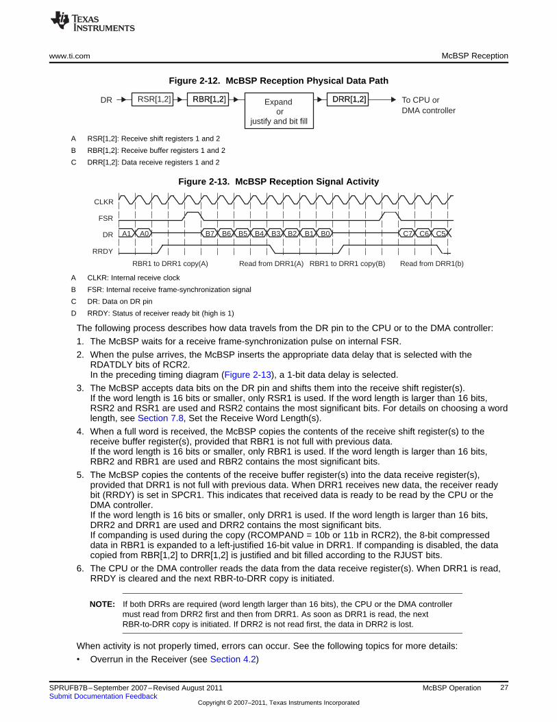
ÁÁÁÁÁÁÁÁÁÁÁÁÁÁÁÁÁÁÁÁÁDR RSR[1,2] Expand
ÁÁÁÁÁÁÁÁÁÁÁÁRBR[1,2] DRR[1,2]DRR[1,2]RBR[1,2] To CPU orDMA controller
justify and bit fillor
RRDY
DR
FSR
CLKR
Read from DRR1(b)RBR1 to DRR1 copy(B)Read from DRR1(A)RBR1 to DRR1 copy(A)
C5C6C7B0B1B2B3B4B5B6B7A0A1
ÁÁÁÁÁÁÁÁÁÁÁÁÁÁÁÁwww.ti.com McBSP Reception
Figure 2-12. McBSP Reception Physical Data Path
A RSR[1,2]: Receive shift registers 1 and 2
B RBR[1,2]: Receive buffer registers 1 and 2
C DRR[1,2]: Data receive registers 1 and 2
Figure 2-13. McBSP Reception Signal Activity
A CLKR: Internal receive clock
B FSR: Internal receive frame-synchronization signal
C DR: Data on DR pin
D RRDY: Status of receiver ready bit (high is 1)
The following process describes how data travels from the DR pin to the CPU or to the DMA controller:
1. The McBSP waits for a receive frame-synchronization pulse on internal FSR.
2. When the pulse arrives, the McBSP inserts the appropriate data delay that is selected with theRDATDLY bits of RCR2.In the preceding timing diagram (Figure 2-13), a 1-bit data delay is selected.
3. The McBSP accepts data bits on the DR pin and shifts them into the receive shift register(s).If the word length is 16 bits or smaller, only RSR1 is used. If the word length is larger than 16 bits,RSR2 and RSR1 are used and RSR2 contains the most significant bits. For details on choosing a wordlength, see Section 7.8, Set the Receive Word Length(s).
4. When a full word is received, the McBSP copies the contents of the receive shift register(s) to thereceive buffer register(s), provided that RBR1 is not full with previous data.If the word length is 16 bits or smaller, only RBR1 is used. If the word length is larger than 16 bits,RBR2 and RBR1 are used and RBR2 contains the most significant bits.
5. The McBSP copies the contents of the receive buffer register(s) into the data receive register(s),provided that DRR1 is not full with previous data. When DRR1 receives new data, the receiver readybit (RRDY) is set in SPCR1. This indicates that received data is ready to be read by the CPU or theDMA controller.If the word length is 16 bits or smaller, only DRR1 is used. If the word length is larger than 16 bits,DRR2 and DRR1 are used and DRR2 contains the most significant bits.If companding is used during the copy (RCOMPAND = 10b or 11b in RCR2), the 8-bit compresseddata in RBR1 is expanded to a left-justified 16-bit value in DRR1. If companding is disabled, the datacopied from RBR[1,2] to DRR[1,2] is justified and bit filled according to the RJUST bits.
6. The CPU or the DMA controller reads the data from the data receive register(s). When DRR1 is read,RRDY is cleared and the next RBR-to-DRR copy is initiated.
NOTE: If both DRRs are required (word length larger than 16 bits), the CPU or the DMA controllermust read from DRR2 first and then from DRR1. As soon as DRR1 is read, the nextRBR-to-DRR copy is initiated. If DRR2 is not read first, the data in DRR2 is lost.
When activity is not properly timed, errors can occur. See the following topics for more details:
• Overrun in the Receiver (see Section 4.2)
27SPRUFB7B–September 2007–Revised August 2011 McBSP OperationSubmit Documentation Feedback
Copyright © 2007–2011, Texas Instruments Incorporated
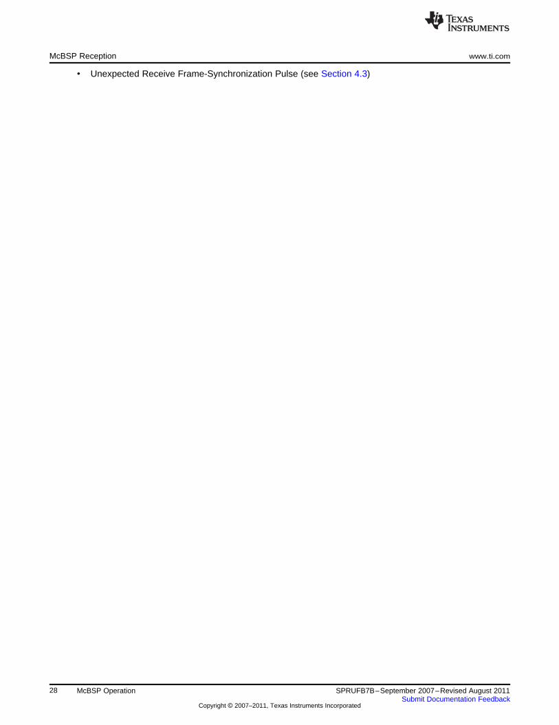
McBSP Reception www.ti.com
• Unexpected Receive Frame-Synchronization Pulse (see Section 4.3)
28 McBSP Operation SPRUFB7B–September 2007–Revised August 2011Submit Documentation Feedback
Copyright © 2007–2011, Texas Instruments Incorporated
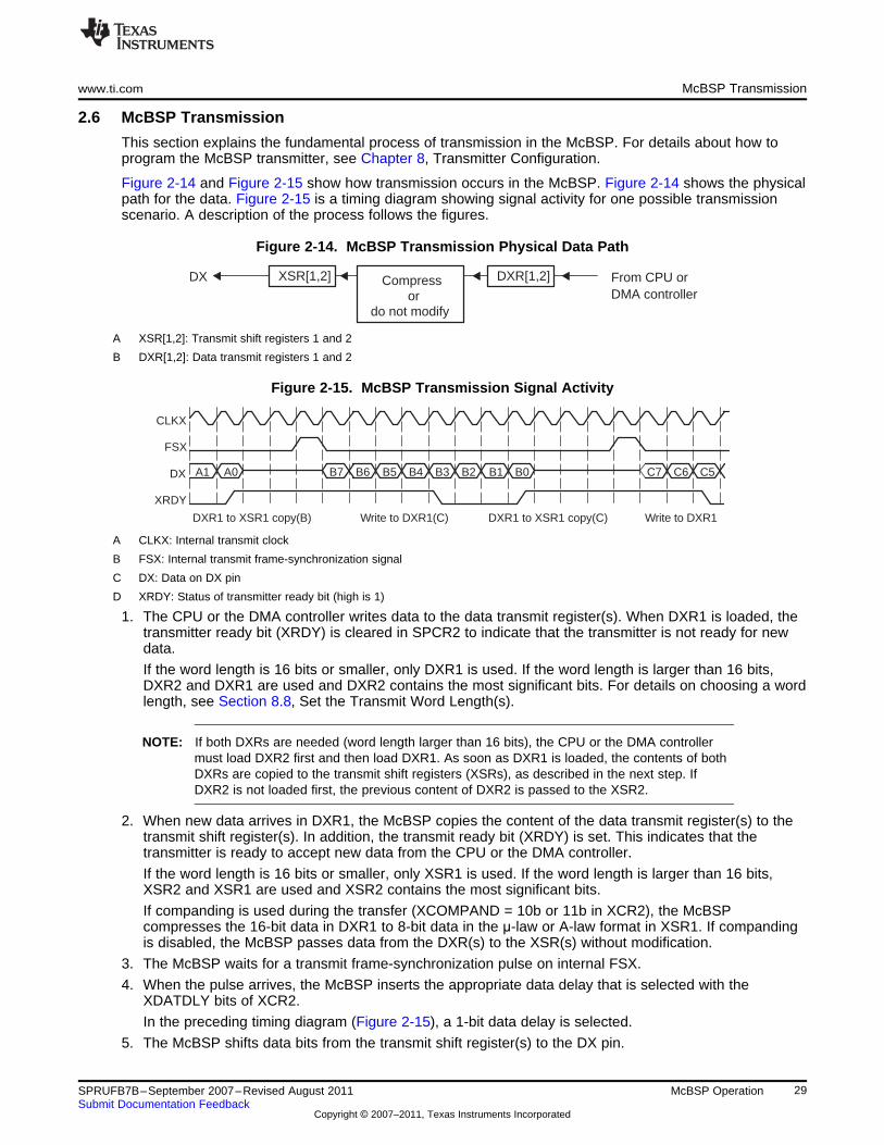
ÁÁÁÁÁÁÁÁÁÁÁÁDX XSR[1,2]
ÁÁÁÁÁÁÁÁÁÁÁÁDXR[1,2] From CPU orDMA controller
Compress
do not modifyor
Write to DXR1DXR1 to XSR1 copy(C)Write to DXR1(C)DXR1 to XSR1 copy(B)
XRDY
DX
FSX
CLKX
C5C6C7B0B1B2B3B4B5B6B7A0A1
ÁÁÁÁÁÁÁÁÁÁÁÁÁÁÁÁÁÁÁÁwww.ti.com McBSP Transmission
2.6 McBSP Transmission
This section explains the fundamental process of transmission in the McBSP. For details about how toprogram the McBSP transmitter, see Chapter 8, Transmitter Configuration.
Figure 2-14 and Figure 2-15 show how transmission occurs in the McBSP. Figure 2-14 shows the physicalpath for the data. Figure 2-15 is a timing diagram showing signal activity for one possible transmissionscenario. A description of the process follows the figures.
Figure 2-14. McBSP Transmission Physical Data Path
A XSR[1,2]: Transmit shift registers 1 and 2
B DXR[1,2]: Data transmit registers 1 and 2
Figure 2-15. McBSP Transmission Signal Activity
A CLKX: Internal transmit clock
B FSX: Internal transmit frame-synchronization signal
C DX: Data on DX pin
D XRDY: Status of transmitter ready bit (high is 1)
1. The CPU or the DMA controller writes data to the data transmit register(s). When DXR1 is loaded, thetransmitter ready bit (XRDY) is cleared in SPCR2 to indicate that the transmitter is not ready for newdata.
If the word length is 16 bits or smaller, only DXR1 is used. If the word length is larger than 16 bits,DXR2 and DXR1 are used and DXR2 contains the most significant bits. For details on choosing a wordlength, see Section 8.8, Set the Transmit Word Length(s).
NOTE: If both DXRs are needed (word length larger than 16 bits), the CPU or the DMA controllermust load DXR2 first and then load DXR1. As soon as DXR1 is loaded, the contents of bothDXRs are copied to the transmit shift registers (XSRs), as described in the next step. IfDXR2 is not loaded first, the previous content of DXR2 is passed to the XSR2.
2. When new data arrives in DXR1, the McBSP copies the content of the data transmit register(s) to thetransmit shift register(s). In addition, the transmit ready bit (XRDY) is set. This indicates that thetransmitter is ready to accept new data from the CPU or the DMA controller.
If the word length is 16 bits or smaller, only XSR1 is used. If the word length is larger than 16 bits,XSR2 and XSR1 are used and XSR2 contains the most significant bits.
If companding is used during the transfer (XCOMPAND = 10b or 11b in XCR2), the McBSPcompresses the 16-bit data in DXR1 to 8-bit data in the μ-law or A-law format in XSR1. If compandingis disabled, the McBSP passes data from the DXR(s) to the XSR(s) without modification.
3. The McBSP waits for a transmit frame-synchronization pulse on internal FSX.
4. When the pulse arrives, the McBSP inserts the appropriate data delay that is selected with theXDATDLY bits of XCR2.
In the preceding timing diagram (Figure 2-15), a 1-bit data delay is selected.
5. The McBSP shifts data bits from the transmit shift register(s) to the DX pin.
29SPRUFB7B–September 2007–Revised August 2011 McBSP OperationSubmit Documentation Feedback
Copyright © 2007–2011, Texas Instruments Incorporated
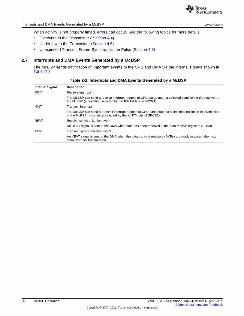
Interrupts and DMA Events Generated by a McBSP www.ti.com
When activity is not properly timed, errors can occur. See the following topics for more details:
• Overwrite in the Transmitter ( Section 4.4)
• Underflow in the Transmitter (Section 4.5)
• Unexpected Transmit Frame-Synchronization Pulse (Section 4.6)
2.7 Interrupts and DMA Events Generated by a McBSP
The McBSP sends notification of important events to the CPU and DMA via the internal signals shown inTable 2-2.
Table 2-2. Interrupts and DMA Events Generated by a McBSP
Internal Signal Description
RINT Receive interrupt
The McBSP can send a receive interrupt request to CPU based upon a selected condition in the receiver ofthe McBSP (a condition selected by the RINTM bits of SPCR1).
XINT Transmit interrupt
The McBSP can send a transmit interrupt request to CPU based upon a selected condition in the transmitterof the McBSP (a condition selected by the XINTM bits of SPCR2).
REVT Receive synchronization event
An REVT signal is sent to the DMA when data has been received in the data receive registers (DRRs).
XEVT Transmit synchronization event
An XEVT signal is sent to the DMA when the data transmit registers (DXRs) are ready to accept the nextserial word for transmission.
30 McBSP Operation SPRUFB7B–September 2007–Revised August 2011Submit Documentation Feedback
Copyright © 2007–2011, Texas Instruments Incorporated
Chapter 3SPRUFB7B–September 2007–Revised August 2011
McBSP Sample Rate Generator
Each McBSP contains a sample rate generator (SRG) that can be programmed to generate an internaldata clock (CLKG) and an internal frame-synchronization signal (FSG). CLKG can be used for bit shiftingon the data receive (DR) pin and/or the data transmit (DX) pin. FSG can be used to initiate frame transferson DR and/or DX. Figure 3-1 is a conceptual block diagram of the sample rate generator.
Topic ........................................................................................................................... Page
3.1 Block Diagram .................................................................................................. 323.2 Frame Synchronization Generation in the Sample Rate Generator .......................... 353.3 Synchronizing Sample Rate Generator Outputs to an External Clock ...................... 353.4 Reset and Initialization Procedure for the Sample Rate Generator ........................... 37
31SPRUFB7B–September 2007–Revised August 2011 McBSP Sample Rate GeneratorSubmit Documentation Feedback
Copyright © 2007–2011, Texas Instruments Incorporated
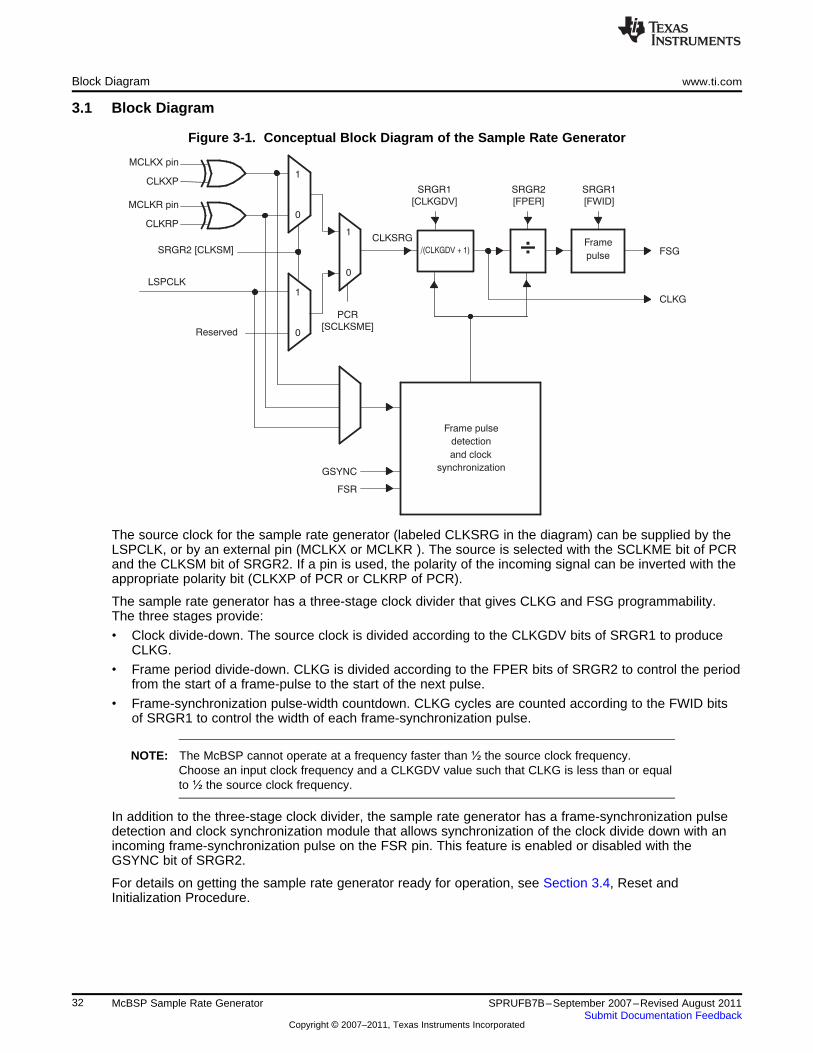
FSR
GSYNC synchronization
and clock
detection
Frame pulse
SRGR1
[CLKGDV]
CLKSRG
0
1CLKXP
MCLKX pin
CLKRP
MCLKR pin
0
1LSPCLK
SRGR2 [CLKSM]
0
1
PCR
[SCLKSME]
SRGR1
[FWID]
CLKG
FSGpulse
Frame
SRGR2
[FPER]
÷
Reserved
/(CLKGDV + 1)
Block Diagram www.ti.com
3.1 Block Diagram
Figure 3-1. Conceptual Block Diagram of the Sample Rate Generator
The source clock for the sample rate generator (labeled CLKSRG in the diagram) can be supplied by theLSPCLK, or by an external pin (MCLKX or MCLKR ). The source is selected with the SCLKME bit of PCRand the CLKSM bit of SRGR2. If a pin is used, the polarity of the incoming signal can be inverted with theappropriate polarity bit (CLKXP of PCR or CLKRP of PCR).
The sample rate generator has a three-stage clock divider that gives CLKG and FSG programmability.The three stages provide:
• Clock divide-down. The source clock is divided according to the CLKGDV bits of SRGR1 to produceCLKG.
• Frame period divide-down. CLKG is divided according to the FPER bits of SRGR2 to control the periodfrom the start of a frame-pulse to the start of the next pulse.
• Frame-synchronization pulse-width countdown. CLKG cycles are counted according to the FWID bitsof SRGR1 to control the width of each frame-synchronization pulse.
NOTE: The McBSP cannot operate at a frequency faster than ½ the source clock frequency.Choose an input clock frequency and a CLKGDV value such that CLKG is less than or equalto ½ the source clock frequency.
In addition to the three-stage clock divider, the sample rate generator has a frame-synchronization pulsedetection and clock synchronization module that allows synchronization of the clock divide down with anincoming frame-synchronization pulse on the FSR pin. This feature is enabled or disabled with theGSYNC bit of SRGR2.
For details on getting the sample rate generator ready for operation, see Section 3.4, Reset andInitialization Procedure.
32 McBSP Sample Rate Generator SPRUFB7B–September 2007–Revised August 2011Submit Documentation Feedback
Copyright © 2007–2011, Texas Instruments Incorporated
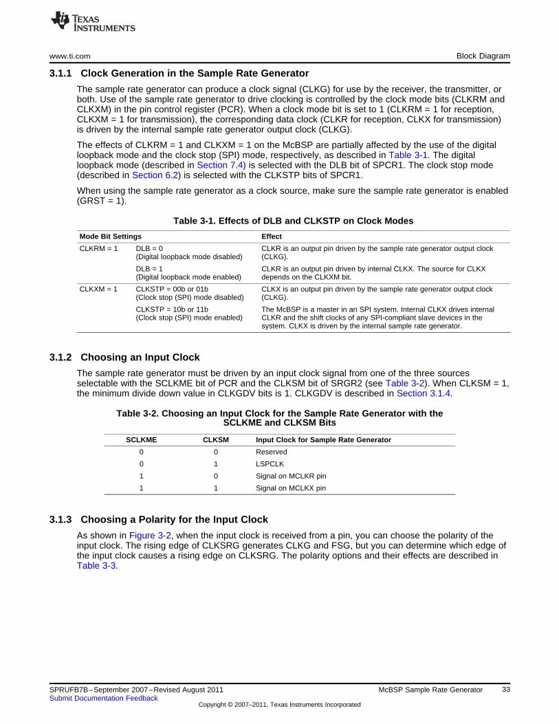
www.ti.com Block Diagram
3.1.1 Clock Generation in the Sample Rate Generator
The sample rate generator can produce a clock signal (CLKG) for use by the receiver, the transmitter, orboth. Use of the sample rate generator to drive clocking is controlled by the clock mode bits (CLKRM andCLKXM) in the pin control register (PCR). When a clock mode bit is set to 1 (CLKRM = 1 for reception,CLKXM = 1 for transmission), the corresponding data clock (CLKR for reception, CLKX for transmission)is driven by the internal sample rate generator output clock (CLKG).
The effects of CLKRM = 1 and CLKXM = 1 on the McBSP are partially affected by the use of the digitalloopback mode and the clock stop (SPI) mode, respectively, as described in Table 3-1. The digitalloopback mode (described in Section 7.4) is selected with the DLB bit of SPCR1. The clock stop mode(described in Section 6.2) is selected with the CLKSTP bits of SPCR1.
When using the sample rate generator as a clock source, make sure the sample rate generator is enabled(GRST = 1).
Table 3-1. Effects of DLB and CLKSTP on Clock Modes
Mode Bit Settings Effect
CLKRM = 1 DLB = 0 CLKR is an output pin driven by the sample rate generator output clock(Digital loopback mode disabled) (CLKG).
DLB = 1 CLKR is an output pin driven by internal CLKX. The source for CLKX(Digital loopback mode enabled) depends on the CLKXM bit.
CLKXM = 1 CLKSTP = 00b or 01b CLKX is an output pin driven by the sample rate generator output clock(Clock stop (SPI) mode disabled) (CLKG).
CLKSTP = 10b or 11b The McBSP is a master in an SPI system. Internal CLKX drives internal(Clock stop (SPI) mode enabled) CLKR and the shift clocks of any SPI-compliant slave devices in the
system. CLKX is driven by the internal sample rate generator.
3.1.2 Choosing an Input Clock
The sample rate generator must be driven by an input clock signal from one of the three sourcesselectable with the SCLKME bit of PCR and the CLKSM bit of SRGR2 (see Table 3-2). When CLKSM = 1,the minimum divide down value in CLKGDV bits is 1. CLKGDV is described in Section 3.1.4.
Table 3-2. Choosing an Input Clock for the Sample Rate Generator with theSCLKME and CLKSM Bits
SCLKME CLKSM Input Clock for Sample Rate Generator
0 0 Reserved
0 1 LSPCLK
1 0 Signal on MCLKR pin
1 1 Signal on MCLKX pin
3.1.3 Choosing a Polarity for the Input Clock
As shown in Figure 3-2, when the input clock is received from a pin, you can choose the polarity of theinput clock. The rising edge of CLKSRG generates CLKG and FSG, but you can determine which edge ofthe input clock causes a rising edge on CLKSRG. The polarity options and their effects are described inTable 3-3.
33SPRUFB7B–September 2007–Revised August 2011 McBSP Sample Rate GeneratorSubmit Documentation Feedback
Copyright © 2007–2011, Texas Instruments Incorporated
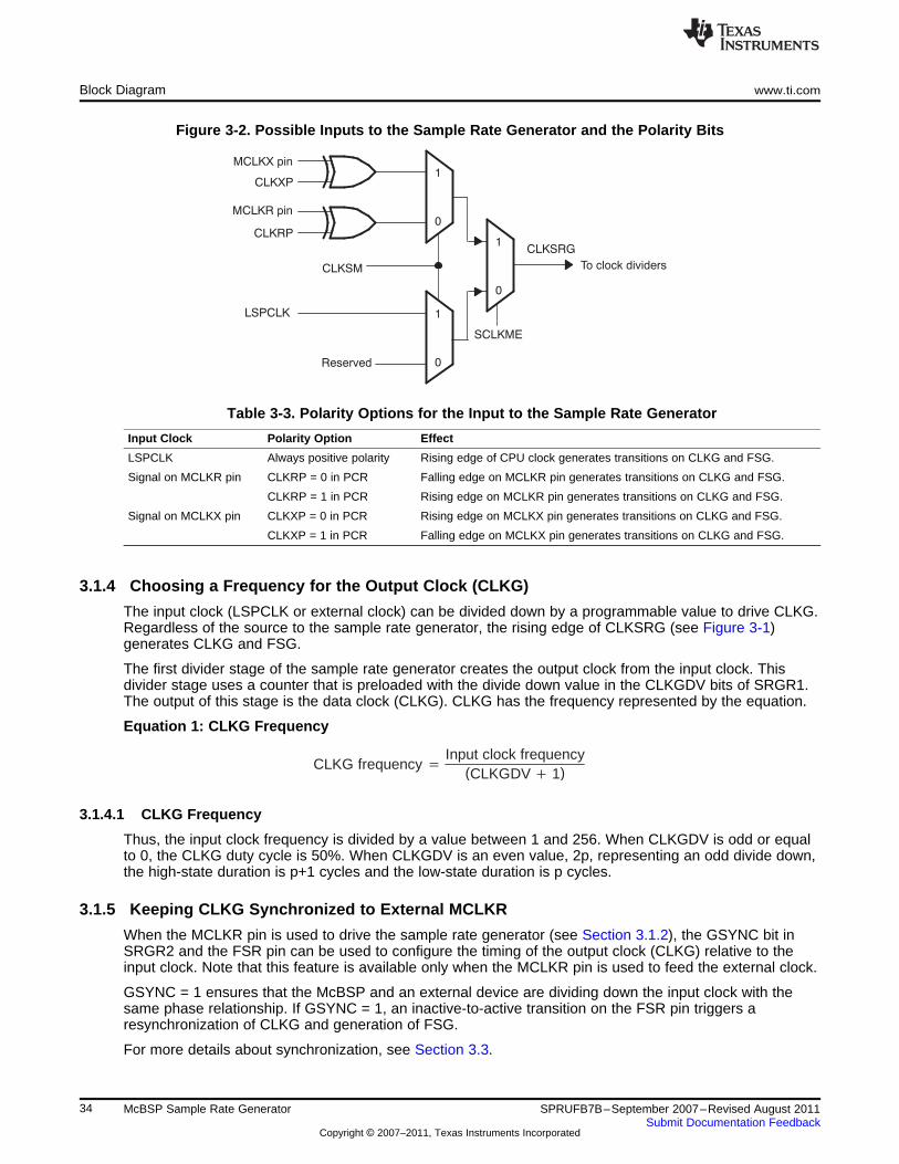
CLKSRG
0
1CLKXP
MCLKX pin
CLKRP
MCLKR pin
0
1LSPCLK
CLKSM
0
1
SCLKME
To clock dividers
Reserved
CLKG frequency �Input clock frequency
(CLKGDV � 1)
Block Diagram www.ti.com
Figure 3-2. Possible Inputs to the Sample Rate Generator and the Polarity Bits
Table 3-3. Polarity Options for the Input to the Sample Rate Generator
Input Clock Polarity Option Effect
LSPCLK Always positive polarity Rising edge of CPU clock generates transitions on CLKG and FSG.
Signal on MCLKR pin CLKRP = 0 in PCR Falling edge on MCLKR pin generates transitions on CLKG and FSG.
CLKRP = 1 in PCR Rising edge on MCLKR pin generates transitions on CLKG and FSG.
Signal on MCLKX pin CLKXP = 0 in PCR Rising edge on MCLKX pin generates transitions on CLKG and FSG.
CLKXP = 1 in PCR Falling edge on MCLKX pin generates transitions on CLKG and FSG.
3.1.4 Choosing a Frequency for the Output Clock (CLKG)
The input clock (LSPCLK or external clock) can be divided down by a programmable value to drive CLKG.Regardless of the source to the sample rate generator, the rising edge of CLKSRG (see Figure 3-1)generates CLKG and FSG.
The first divider stage of the sample rate generator creates the output clock from the input clock. Thisdivider stage uses a counter that is preloaded with the divide down value in the CLKGDV bits of SRGR1.The output of this stage is the data clock (CLKG). CLKG has the frequency represented by the equation.
Equation 1: CLKG Frequency
3.1.4.1 CLKG Frequency
Thus, the input clock frequency is divided by a value between 1 and 256. When CLKGDV is odd or equalto 0, the CLKG duty cycle is 50%. When CLKGDV is an even value, 2p, representing an odd divide down,the high-state duration is p+1 cycles and the low-state duration is p cycles.
3.1.5 Keeping CLKG Synchronized to External MCLKR
When the MCLKR pin is used to drive the sample rate generator (see Section 3.1.2), the GSYNC bit inSRGR2 and the FSR pin can be used to configure the timing of the output clock (CLKG) relative to theinput clock. Note that this feature is available only when the MCLKR pin is used to feed the external clock.
GSYNC = 1 ensures that the McBSP and an external device are dividing down the input clock with thesame phase relationship. If GSYNC = 1, an inactive-to-active transition on the FSR pin triggers aresynchronization of CLKG and generation of FSG.
For more details about synchronization, see Section 3.3.
34 McBSP Sample Rate Generator SPRUFB7B–September 2007–Revised August 2011Submit Documentation Feedback
Copyright © 2007–2011, Texas Instruments Incorporated
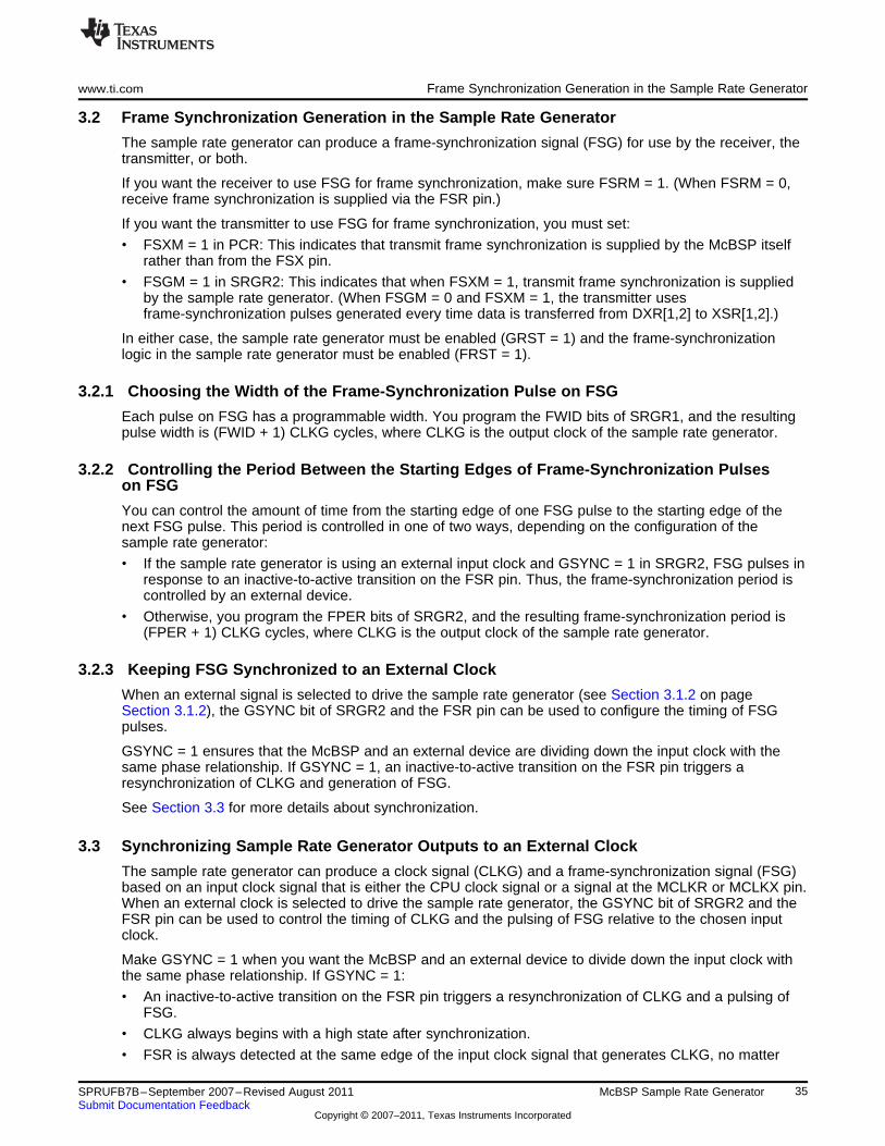
www.ti.com Frame Synchronization Generation in the Sample Rate Generator
3.2 Frame Synchronization Generation in the Sample Rate Generator
The sample rate generator can produce a frame-synchronization signal (FSG) for use by the receiver, thetransmitter, or both.
If you want the receiver to use FSG for frame synchronization, make sure FSRM = 1. (When FSRM = 0,receive frame synchronization is supplied via the FSR pin.)
If you want the transmitter to use FSG for frame synchronization, you must set:
• FSXM = 1 in PCR: This indicates that transmit frame synchronization is supplied by the McBSP itselfrather than from the FSX pin.
• FSGM = 1 in SRGR2: This indicates that when FSXM = 1, transmit frame synchronization is suppliedby the sample rate generator. (When FSGM = 0 and FSXM = 1, the transmitter usesframe-synchronization pulses generated every time data is transferred from DXR[1,2] to XSR[1,2].)
In either case, the sample rate generator must be enabled (GRST = 1) and the frame-synchronizationlogic in the sample rate generator must be enabled (FRST = 1).
3.2.1 Choosing the Width of the Frame-Synchronization Pulse on FSG
Each pulse on FSG has a programmable width. You program the FWID bits of SRGR1, and the resultingpulse width is (FWID + 1) CLKG cycles, where CLKG is the output clock of the sample rate generator.
3.2.2 Controlling the Period Between the Starting Edges of Frame-Synchronization Pulseson FSG
You can control the amount of time from the starting edge of one FSG pulse to the starting edge of thenext FSG pulse. This period is controlled in one of two ways, depending on the configuration of thesample rate generator:
• If the sample rate generator is using an external input clock and GSYNC = 1 in SRGR2, FSG pulses inresponse to an inactive-to-active transition on the FSR pin. Thus, the frame-synchronization period iscontrolled by an external device.
• Otherwise, you program the FPER bits of SRGR2, and the resulting frame-synchronization period is(FPER + 1) CLKG cycles, where CLKG is the output clock of the sample rate generator.
3.2.3 Keeping FSG Synchronized to an External Clock
When an external signal is selected to drive the sample rate generator (see Section 3.1.2 on pageSection 3.1.2), the GSYNC bit of SRGR2 and the FSR pin can be used to configure the timing of FSGpulses.
GSYNC = 1 ensures that the McBSP and an external device are dividing down the input clock with thesame phase relationship. If GSYNC = 1, an inactive-to-active transition on the FSR pin triggers aresynchronization of CLKG and generation of FSG.
See Section 3.3 for more details about synchronization.
3.3 Synchronizing Sample Rate Generator Outputs to an External Clock
The sample rate generator can produce a clock signal (CLKG) and a frame-synchronization signal (FSG)based on an input clock signal that is either the CPU clock signal or a signal at the MCLKR or MCLKX pin.When an external clock is selected to drive the sample rate generator, the GSYNC bit of SRGR2 and theFSR pin can be used to control the timing of CLKG and the pulsing of FSG relative to the chosen inputclock.
Make GSYNC = 1 when you want the McBSP and an external device to divide down the input clock withthe same phase relationship. If GSYNC = 1:
• An inactive-to-active transition on the FSR pin triggers a resynchronization of CLKG and a pulsing ofFSG.
• CLKG always begins with a high state after synchronization.
• FSR is always detected at the same edge of the input clock signal that generates CLKG, no matter
35SPRUFB7B–September 2007–Revised August 2011 McBSP Sample Rate GeneratorSubmit Documentation Feedback
Copyright © 2007–2011, Texas Instruments Incorporated
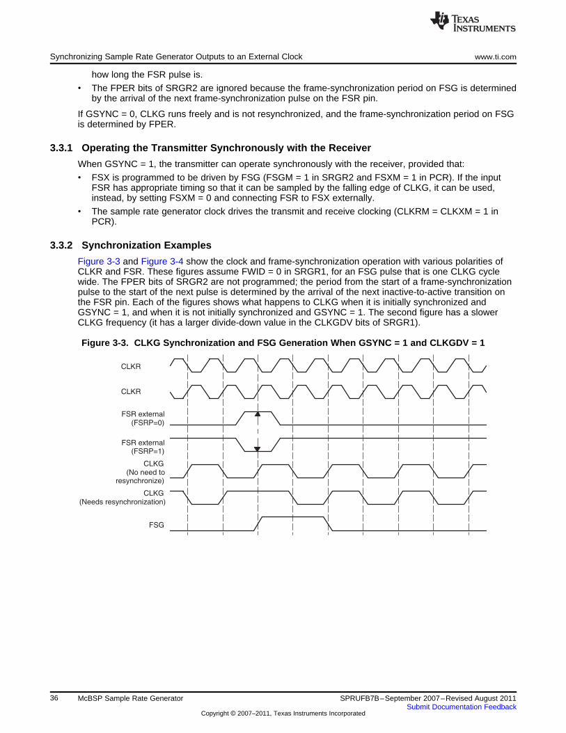
FSG
(Needs resynchronization)CLKG
resynchronize)(No need to
CLKG
(FSRP=1)FSR external
(FSRP=0)FSR external
CLKR
CLKR
Synchronizing Sample Rate Generator Outputs to an External Clock www.ti.com
how long the FSR pulse is.
• The FPER bits of SRGR2 are ignored because the frame-synchronization period on FSG is determinedby the arrival of the next frame-synchronization pulse on the FSR pin.
If GSYNC = 0, CLKG runs freely and is not resynchronized, and the frame-synchronization period on FSGis determined by FPER.
3.3.1 Operating the Transmitter Synchronously with the Receiver
When GSYNC = 1, the transmitter can operate synchronously with the receiver, provided that:
• FSX is programmed to be driven by FSG (FSGM = 1 in SRGR2 and FSXM = 1 in PCR). If the inputFSR has appropriate timing so that it can be sampled by the falling edge of CLKG, it can be used,instead, by setting FSXM = 0 and connecting FSR to FSX externally.
• The sample rate generator clock drives the transmit and receive clocking (CLKRM = CLKXM = 1 inPCR).
3.3.2 Synchronization Examples
Figure 3-3 and Figure 3-4 show the clock and frame-synchronization operation with various polarities ofCLKR and FSR. These figures assume FWID = 0 in SRGR1, for an FSG pulse that is one CLKG cyclewide. The FPER bits of SRGR2 are not programmed; the period from the start of a frame-synchronizationpulse to the start of the next pulse is determined by the arrival of the next inactive-to-active transition onthe FSR pin. Each of the figures shows what happens to CLKG when it is initially synchronized andGSYNC = 1, and when it is not initially synchronized and GSYNC = 1. The second figure has a slowerCLKG frequency (it has a larger divide-down value in the CLKGDV bits of SRGR1).
Figure 3-3. CLKG Synchronization and FSG Generation When GSYNC = 1 and CLKGDV = 1
36 McBSP Sample Rate Generator SPRUFB7B–September 2007–Revised August 2011Submit Documentation Feedback
Copyright © 2007–2011, Texas Instruments Incorporated
FSG
(Needs resynchronization)CLKG
resynchronize)(No need to
CLKG
(FSRP=1)FSR external
(FSRP=0)FSR external
CLKR
CLKR
www.ti.com Reset and Initialization Procedure for the Sample Rate Generator
Figure 3-4. CLKG Synchronization and FSG Generation When GSYNC = 1 and CLKGDV = 3
3.4 Reset and Initialization Procedure for the Sample Rate Generator
To reset and initialize the sample rate generator:
Step 1. Place the McBSP/sample rate generator in reset.
During a DSP reset, the sample rate generator, the receiver, and the transmitter reset bits (GRST,RRST, and XRST) are automatically forced to 0. Otherwise, during normal operation, the sample rategenerator can be reset by making GRST = 0 in SPCR2, provided that CLKG and/or FSG is not usedby any portion of the McBSP. Depending on your system you may also want to reset the receiver(RRST = 0 in SPCR1) and reset the transmitter (XRST = 0 in SPCR2).
If GRST = 0 due to a device reset, CLKG is driven by the CPU clock divided by 2, and FSG is driveninactive-low. If GRST = 0 due to program code, CLKG and FSG are driven low (inactive).
Step 2. Program the registers that affect the sample rate generator.
Program the sample rate generator registers (SRGR1 and SRGR2) as required for your application. Ifnecessary, other control registers can be loaded with desired values, provided the respective portion ofthe McBSP (the receiver or transmitter) is in reset.
After the sample rate generator registers are programmed, wait 2 CLKSRG cycles. This ensuresproper synchronization internally.
Step 3. Enable the sample rate generator (take it out of reset).
In SPCR2, make GRST = 1 to enable the sample rate generator.
After the sample rate generator is enabled, wait two CLKG cycles for the sample rate generator logic tostabilize.
On the next rising edge of CLKSRG, CLKG transitions to 1 and starts clocking with a frequency equalto .
Table 3-4. Input Clock Selection for Sample Rate Generator
SCLKME CLKSM Input Clock for Sample Rate Generator
0 0 Reserved
0 1 LSPCLK
1 0 Signal on MCLKR pin
1 1 Signal on MCLKX pin
37SPRUFB7B–September 2007–Revised August 2011 McBSP Sample Rate GeneratorSubmit Documentation Feedback
Copyright © 2007–2011, Texas Instruments Incorporated
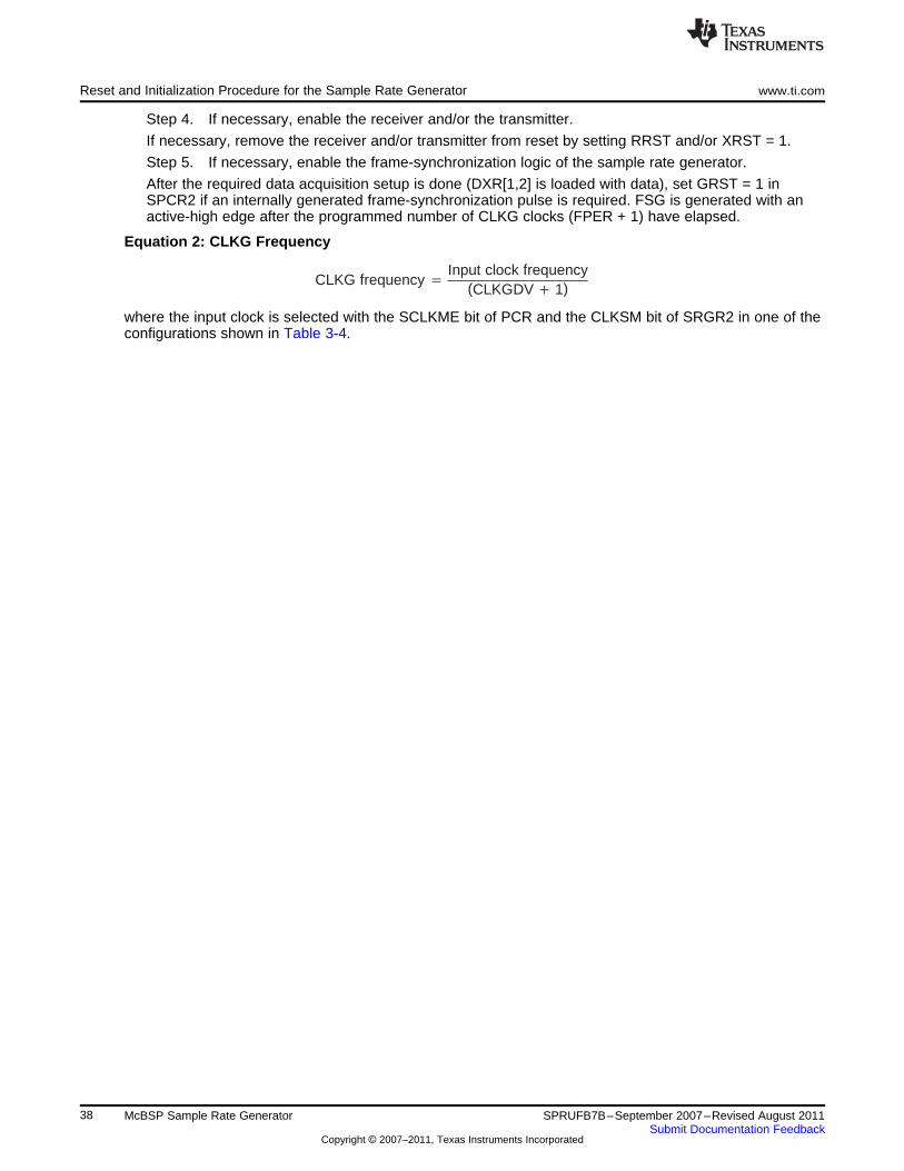
CLKG frequency �Input clock frequency
(CLKGDV � 1)
Reset and Initialization Procedure for the Sample Rate Generator www.ti.com
Step 4. If necessary, enable the receiver and/or the transmitter.
If necessary, remove the receiver and/or transmitter from reset by setting RRST and/or XRST = 1.
Step 5. If necessary, enable the frame-synchronization logic of the sample rate generator.
After the required data acquisition setup is done (DXR[1,2] is loaded with data), set GRST = 1 inSPCR2 if an internally generated frame-synchronization pulse is required. FSG is generated with anactive-high edge after the programmed number of CLKG clocks (FPER + 1) have elapsed.
Equation 2: CLKG Frequency
where the input clock is selected with the SCLKME bit of PCR and the CLKSM bit of SRGR2 in one of theconfigurations shown in Table 3-4.
38 McBSP Sample Rate Generator SPRUFB7B–September 2007–Revised August 2011Submit Documentation Feedback
Copyright © 2007–2011, Texas Instruments Incorporated
Chapter 4SPRUFB7B–September 2007–Revised August 2011
McBSP Exception/Error Conditions
This chapter describes exception/error conditions and how to handle them.
Topic ........................................................................................................................... Page
4.1 Types of Errors ................................................................................................. 404.2 Overrun in the Receiver ..................................................................................... 404.3 Unexpected Receive Frame-Synchronization Pulse ............................................... 414.4 Overwrite in the Transmitter ............................................................................... 444.5 Underflow in the Transmitter .............................................................................. 444.6 Unexpected Transmit Frame-Synchronization Pulse .............................................. 45
39SPRUFB7B–September 2007–Revised August 2011 McBSP Exception/Error ConditionsSubmit Documentation Feedback
Copyright © 2007–2011, Texas Instruments Incorporated
Types of Errors www.ti.com
4.1 Types of Errors
There are five serial port events that can constitute a system error:
• Receiver overrun (RFULL = 1)
This occurs when DRR1 has not been read since the last RBR-to-DRR copy. Consequently, thereceiver does not copy a new word from the RBR(s) to the DRR(s) and the RSR(s) are now full withanother new word shifted in from DR. Therefore, RFULL = 1 indicates an error condition wherein anynew data that can arrive at this time on DR replaces the contents of the RSR(s), and the previous wordis lost. The RSRs continue to be overwritten as long as new data arrives on DR and DRR1 is not read.For more details about overrun in the receiver, see Section 4.2.
• Unexpected receive frame-synchronization pulse (RSYNCERR = 1)
This occurs during reception when RFIG = 0 and an unexpected frame-synchronization pulse occurs.An unexpected frame-synchronization pulse is one that begins the next frame transfer before all thebits of the current frame have been received. Such a pulse causes data reception to abort and restart.If new data has been copied into the RBR(s) from the RSR(s) since the last RBR-to-DRR copy, thisnew data in the RBR(s) is lost. This is because no RBR-to-DRR copy occurs; the reception has beenrestarted. For more details about receive frame-synchronization errors, see Section 4.3.
• Transmitter data overwrite
This occurs when the CPU or DMA controller overwrites data in the DXR(s) before the data is copiedto the XSR(s). The overwritten data never reaches the DX pin. For more details about overwrite in thetransmitter, see Section 4.4.
• Transmitter underflow (XEMPTY = 0)
If a new frame-synchronization signal arrives before new data is loaded into DXR1, the previous datain the DXR(s) is sent again. This procedure continues for every new frame-synchronization pulse thatarrives until DXR1 is loaded with new data. For more details about underflow in the transmitter, seeSection 4.5.
• Unexpected transmit frame-synchronization pulse (XSYNCERR = 1)
This occurs during transmission when XFIG = 0 and an unexpected frame-synchronization pulseoccurs. An unexpected frame-synchronization pulse is one that begins the next frame transfer beforeall the bits of the current frame have been transferred. Such a pulse causes the current datatransmission to abort and restart. If new data has been written to the DXR(s) since the lastDXR-to-XSR copy, the current value in the XSR(s) is lost. For more details about transmitframe-synchronization errors, see Section 4.6.
4.2 Overrun in the Receiver
RFULL = 1 in SPCR1 indicates that the receiver has experienced overrun and is in an error condition.RFULL is set when all of the following conditions are met:
1. DRR1 has not been read since the last RBR-to-DRR copy (RRDY = 1).
2. RBR1 is full and an RBR-to-DRR copy has not occurred.
3. RSR1 is full and an RSR1-to-RBR copy has not occurred.
As described in the Section 2.5, McBSP Reception, data arriving on DR is continuously shifted into RSR1(for word length of 16 bits or smaller) or RSR2 and RSR1 (for word length larger than 16 bits). Once acomplete word is shifted into the RSR(s), an RSR-to-RBR copy can occur only if the previous data inRBR1 has been copied to DRR1. The RRDY bit is set when new data arrives in DRR1 and is clearedwhen that data is read from DRR1. Until RRDY = 0, the next RBR-to-DRR copy does not take place, andthe data is held in the RSR(s). New data arriving on the DR pin is shifted into RSR(s), and the previouscontent of the RSR(s) is lost.
You can prevent the loss of data if DRR1 is read no later than 2.5 cycles before the end of the third wordis shifted into the RSR1.
NOTE: If both DRRs are needed (word length larger than 16 bits), the CPU or the DMA controllermust read from DRR2 first and then from DRR1. As soon as DRR1 is read, the nextRBR-to-DRR copy is initiated. If DRR2 is not read first, the data in DRR2 is lost.
40 McBSP Exception/Error Conditions SPRUFB7B–September 2007–Revised August 2011Submit Documentation Feedback
Copyright © 2007–2011, Texas Instruments Incorporated
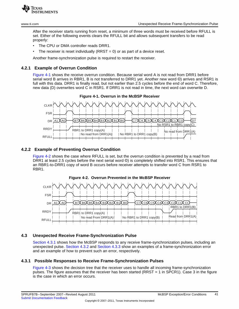
No RSR1 to RBR1 copy(C)
No read from DRR1(A)No RBR1 to DRR1 copy(B)No read from DRR1(A)
RBR1 to DRR1 copy(A)
D7C0C1C2C3C4C5C6C7B0B1B2B3B4B5B6B7A0A1
RFULL
RRDY
DR
FSR
CLKR ÁÁÁÁ ÁÁÁÁÁÁÁÁÁÁÁÁÁÁÁÁÁÁÁÁÁÁÁÁRBR1 to DRR1(B)
No RBR1 to DRR1 copy(B)No read From DRR1(A)RBR1 to DRR1 copy(A)
C0C1C2C3C4C5C6C7B0B1B2B3B4B5B6B7A0A1
RFULL
RRDY
DR
FSR
CLKR ÁÁÁ ÁÁÁÁÁÁÁÁÁÁÁÁRead from DRR1(A)
www.ti.com Unexpected Receive Frame-Synchronization Pulse
After the receiver starts running from reset, a minimum of three words must be received before RFULL isset. Either of the following events clears the RFULL bit and allows subsequent transfers to be readproperly:
• The CPU or DMA controller reads DRR1.
• The receiver is reset individually (RRST = 0) or as part of a device reset.
Another frame-synchronization pulse is required to restart the receiver.
4.2.1 Example of Overrun Condition
Figure 4-1 shows the receive overrun condition. Because serial word A is not read from DRR1 beforeserial word B arrives in RBR1, B is not transferred to DRR1 yet. Another new word ©) arrives and RSR1 isfull with this data. DRR1 is finally read, but not earlier than 2.5 cycles before the end of word C. Therefore,new data (D) overwrites word C in RSR1. If DRR1 is not read in time, the next word can overwrite D.
Figure 4-1. Overrun in the McBSP Receiver
4.2.2 Example of Preventing Overrun Condition
Figure 4-2 shows the case where RFULL is set, but the overrun condition is prevented by a read fromDRR1 at least 2.5 cycles before the next serial word ©) is completely shifted into RSR1. This ensures thatan RBR1-to-DRR1 copy of word B occurs before receiver attempts to transfer word C from RSR1 toRBR1.
Figure 4-2. Overrun Prevented in the McBSP Receiver
4.3 Unexpected Receive Frame-Synchronization Pulse
Section 4.3.1 shows how the McBSP responds to any receive frame-synchronization pulses, including anunexpected pulse. Section 4.3.2 and Section 4.3.3 show an examples of a frame-synchronization errorand an example of how to prevent such an error, respectively.
4.3.1 Possible Responses to Receive Frame-Synchronization Pulses
Figure 4-3 shows the decision tree that the receiver uses to handle all incoming frame-synchronizationpulses. The figure assumes that the receiver has been started (RRST = 1 in SPCR1). Case 3 in the figureis the case in which an error occurs.
41SPRUFB7B–September 2007–Revised August 2011 McBSP Exception/Error ConditionsSubmit Documentation Feedback
Copyright © 2007–2011, Texas Instruments Incorporated
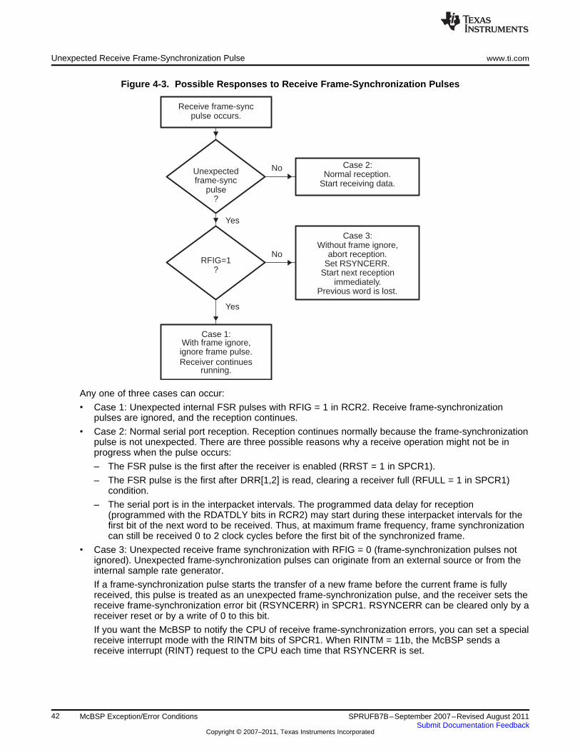
Yes
No
Yes
No
running.Receiver continuesignore frame pulse.With frame ignore,
Case 1:
ÁÁÁÁÁÁÁÁÁÁÁÁÁÁÁÁÁÁÁÁÁÁÁÁÁÁÁÁÁÁÁÁÁÁÁÁÁÁÁÁÁÁÁÁÁÁÁÁÁÁÁÁÁÁÁÁÁÁÁÁÁÁÁÁÁÁÁÁÁÁÁÁÁÁÁÁÁÁÁÁPrevious word is lost.immediately.
Start next receptionSet RSYNCERR.abort reception.
Without frame ignore,Case 3:
Start receiving data.Normal reception.
Case 2:
ÁÁÁÁÁÁÁÁÁÁÁÁÁÁÁÁÁÁÁÁÁÁÁÁÁÁÁÁÁÁÁÁÁÁÁÁÁÁÁÁÁÁÁÁÁpulse occurs.Receive frame-sync
?RFIG=1
ÁÁÁÁÁÁÁÁÁÁÁÁÁÁÁÁÁÁÁÁÁÁÁÁÁÁÁÁÁÁÁÁÁÁÁÁÁÁÁÁÁÁÁÁÁÁÁÁÁÁÁÁÁÁÁÁ?pulse
frame-syncUnexpected
Unexpected Receive Frame-Synchronization Pulse www.ti.com
Figure 4-3. Possible Responses to Receive Frame-Synchronization Pulses
Any one of three cases can occur:
• Case 1: Unexpected internal FSR pulses with RFIG = 1 in RCR2. Receive frame-synchronizationpulses are ignored, and the reception continues.
• Case 2: Normal serial port reception. Reception continues normally because the frame-synchronizationpulse is not unexpected. There are three possible reasons why a receive operation might not be inprogress when the pulse occurs:
– The FSR pulse is the first after the receiver is enabled (RRST = 1 in SPCR1).
– The FSR pulse is the first after DRR[1,2] is read, clearing a receiver full (RFULL = 1 in SPCR1)condition.
– The serial port is in the interpacket intervals. The programmed data delay for reception(programmed with the RDATDLY bits in RCR2) may start during these interpacket intervals for thefirst bit of the next word to be received. Thus, at maximum frame frequency, frame synchronizationcan still be received 0 to 2 clock cycles before the first bit of the synchronized frame.
• Case 3: Unexpected receive frame synchronization with RFIG = 0 (frame-synchronization pulses notignored). Unexpected frame-synchronization pulses can originate from an external source or from theinternal sample rate generator.
If a frame-synchronization pulse starts the transfer of a new frame before the current frame is fullyreceived, this pulse is treated as an unexpected frame-synchronization pulse, and the receiver sets thereceive frame-synchronization error bit (RSYNCERR) in SPCR1. RSYNCERR can be cleared only by areceiver reset or by a write of 0 to this bit.
If you want the McBSP to notify the CPU of receive frame-synchronization errors, you can set a specialreceive interrupt mode with the RINTM bits of SPCR1. When RINTM = 11b, the McBSP sends areceive interrupt (RINT) request to the CPU each time that RSYNCERR is set.
42 McBSP Exception/Error Conditions SPRUFB7B–September 2007–Revised August 2011Submit Documentation Feedback
Copyright © 2007–2011, Texas Instruments Incorporated
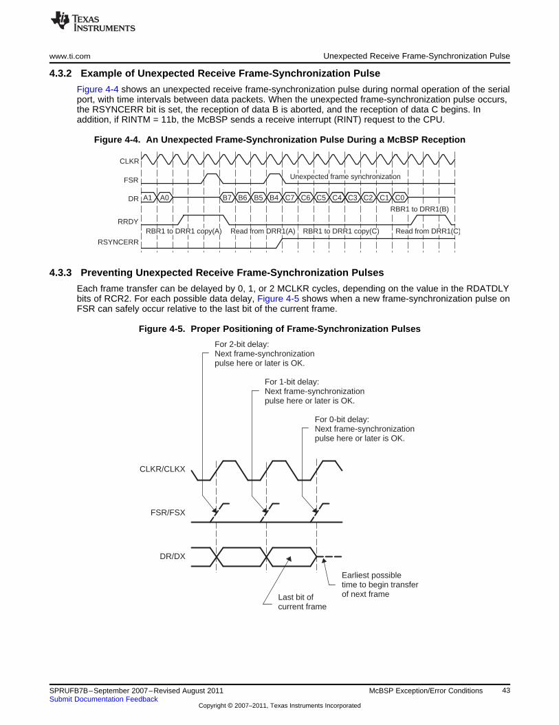
ÁÁÁÁÁÁÁÁÁÁÁÁÁÁÁÁ Unexpected frame synchronization
RBR1 to DRR1(B)
C0C1C2C3C4C5C6C7B4B5B6B7A0A1
RSYNCERR
RRDY
DR
FSR
CLKR
Read from DRR1(C)RBR1 to DRR1 copy(C)Read from DRR1(A)RBR1 to DRR1 copy(A)
For 2-bit delay:Next frame-synchronizationpulse here or later is OK.
For 1-bit delay:Next frame-synchronizationpulse here or later is OK.
For 0-bit delay:Next frame-synchronizationpulse here or later is OK.
CLKR/CLKX
FSR/FSX
DR/DX
Last bit ofcurrent frame
Earliest possibletime to begin transferof next frame
www.ti.com Unexpected Receive Frame-Synchronization Pulse
4.3.2 Example of Unexpected Receive Frame-Synchronization Pulse
Figure 4-4 shows an unexpected receive frame-synchronization pulse during normal operation of the serialport, with time intervals between data packets. When the unexpected frame-synchronization pulse occurs,the RSYNCERR bit is set, the reception of data B is aborted, and the reception of data C begins. Inaddition, if RINTM = 11b, the McBSP sends a receive interrupt (RINT) request to the CPU.
Figure 4-4. An Unexpected Frame-Synchronization Pulse During a McBSP Reception
4.3.3 Preventing Unexpected Receive Frame-Synchronization Pulses
Each frame transfer can be delayed by 0, 1, or 2 MCLKR cycles, depending on the value in the RDATDLYbits of RCR2. For each possible data delay, Figure 4-5 shows when a new frame-synchronization pulse onFSR can safely occur relative to the last bit of the current frame.
Figure 4-5. Proper Positioning of Frame-Synchronization Pulses
43SPRUFB7B–September 2007–Revised August 2011 McBSP Exception/Error ConditionsSubmit Documentation Feedback
Copyright © 2007–2011, Texas Instruments Incorporated
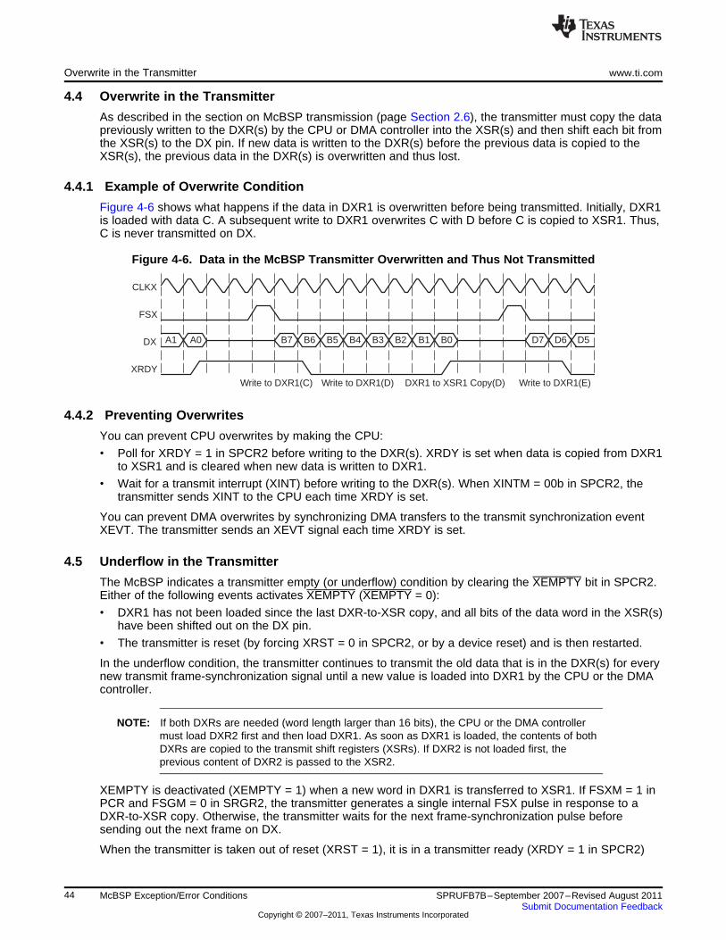
Write to DXR1(D)
ÁÁÁÁ ÁÁÁÁWrite to DXR1(E)DXR1 to XSR1 Copy(D)Write to DXR1(C)
D5D6D7B0B1B2B3B4B5B6B7A0A1
XRDY
DX
FSX
CLKX ÁÁÁÁÁÁÁÁOverwrite in the Transmitter www.ti.com
4.4 Overwrite in the Transmitter
As described in the section on McBSP transmission (page Section 2.6), the transmitter must copy the datapreviously written to the DXR(s) by the CPU or DMA controller into the XSR(s) and then shift each bit fromthe XSR(s) to the DX pin. If new data is written to the DXR(s) before the previous data is copied to theXSR(s), the previous data in the DXR(s) is overwritten and thus lost.
4.4.1 Example of Overwrite Condition
Figure 4-6 shows what happens if the data in DXR1 is overwritten before being transmitted. Initially, DXR1is loaded with data C. A subsequent write to DXR1 overwrites C with D before C is copied to XSR1. Thus,C is never transmitted on DX.
Figure 4-6. Data in the McBSP Transmitter Overwritten and Thus Not Transmitted
4.4.2 Preventing Overwrites
You can prevent CPU overwrites by making the CPU:
• Poll for XRDY = 1 in SPCR2 before writing to the DXR(s). XRDY is set when data is copied from DXR1to XSR1 and is cleared when new data is written to DXR1.
• Wait for a transmit interrupt (XINT) before writing to the DXR(s). When XINTM = 00b in SPCR2, thetransmitter sends XINT to the CPU each time XRDY is set.
You can prevent DMA overwrites by synchronizing DMA transfers to the transmit synchronization eventXEVT. The transmitter sends an XEVT signal each time XRDY is set.
4.5 Underflow in the Transmitter
The McBSP indicates a transmitter empty (or underflow) condition by clearing the XEMPTY bit in SPCR2.Either of the following events activates XEMPTY (XEMPTY = 0):
• DXR1 has not been loaded since the last DXR-to-XSR copy, and all bits of the data word in the XSR(s)have been shifted out on the DX pin.
• The transmitter is reset (by forcing XRST = 0 in SPCR2, or by a device reset) and is then restarted.
In the underflow condition, the transmitter continues to transmit the old data that is in the DXR(s) for everynew transmit frame-synchronization signal until a new value is loaded into DXR1 by the CPU or the DMAcontroller.
NOTE: If both DXRs are needed (word length larger than 16 bits), the CPU or the DMA controllermust load DXR2 first and then load DXR1. As soon as DXR1 is loaded, the contents of bothDXRs are copied to the transmit shift registers (XSRs). If DXR2 is not loaded first, theprevious content of DXR2 is passed to the XSR2.
XEMPTY is deactivated (XEMPTY = 1) when a new word in DXR1 is transferred to XSR1. If FSXM = 1 inPCR and FSGM = 0 in SRGR2, the transmitter generates a single internal FSX pulse in response to aDXR-to-XSR copy. Otherwise, the transmitter waits for the next frame-synchronization pulse beforesending out the next frame on DX.
When the transmitter is taken out of reset (XRST = 1), it is in a transmitter ready (XRDY = 1 in SPCR2)
44 McBSP Exception/Error Conditions SPRUFB7B–September 2007–Revised August 2011Submit Documentation Feedback
Copyright © 2007–2011, Texas Instruments Incorporated
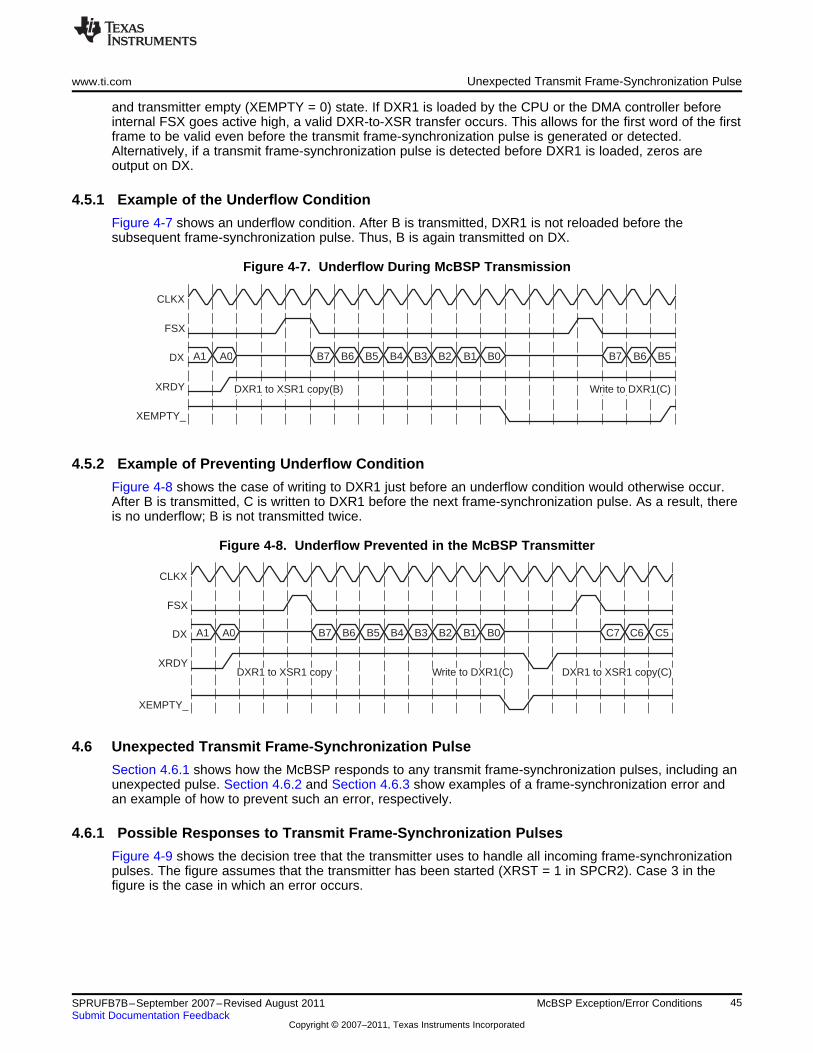
XEMPTY_
ÁÁÁ ÁÁÁ B5B6B7B0B1B2B3B4B5B6B7A0A1
XRDY
DX
FSX
CLKX ÁÁÁÁÁÁWrite to DXR1(C)DXR1 to XSR1 copy(B)
XEMPTY_
ÁÁÁ ÁÁÁ C5C6C7B0B1B2B3B4B5B6B7A0A1
XRDY
DX
FSX
CLKX ÁÁÁÁÁÁDXR1 to XSR1 copy(C)Write to DXR1(C)DXR1 to XSR1 copy
www.ti.com Unexpected Transmit Frame-Synchronization Pulse
and transmitter empty (XEMPTY = 0) state. If DXR1 is loaded by the CPU or the DMA controller beforeinternal FSX goes active high, a valid DXR-to-XSR transfer occurs. This allows for the first word of the firstframe to be valid even before the transmit frame-synchronization pulse is generated or detected.Alternatively, if a transmit frame-synchronization pulse is detected before DXR1 is loaded, zeros areoutput on DX.
4.5.1 Example of the Underflow Condition
Figure 4-7 shows an underflow condition. After B is transmitted, DXR1 is not reloaded before thesubsequent frame-synchronization pulse. Thus, B is again transmitted on DX.
Figure 4-7. Underflow During McBSP Transmission
4.5.2 Example of Preventing Underflow Condition
Figure 4-8 shows the case of writing to DXR1 just before an underflow condition would otherwise occur.After B is transmitted, C is written to DXR1 before the next frame-synchronization pulse. As a result, thereis no underflow; B is not transmitted twice.
Figure 4-8. Underflow Prevented in the McBSP Transmitter
4.6 Unexpected Transmit Frame-Synchronization Pulse
Section 4.6.1 shows how the McBSP responds to any transmit frame-synchronization pulses, including anunexpected pulse. Section 4.6.2 and Section 4.6.3 show examples of a frame-synchronization error andan example of how to prevent such an error, respectively.
4.6.1 Possible Responses to Transmit Frame-Synchronization Pulses
Figure 4-9 shows the decision tree that the transmitter uses to handle all incoming frame-synchronizationpulses. The figure assumes that the transmitter has been started (XRST = 1 in SPCR2). Case 3 in thefigure is the case in which an error occurs.
45SPRUFB7B–September 2007–Revised August 2011 McBSP Exception/Error ConditionsSubmit Documentation Feedback
Copyright © 2007–2011, Texas Instruments Incorporated
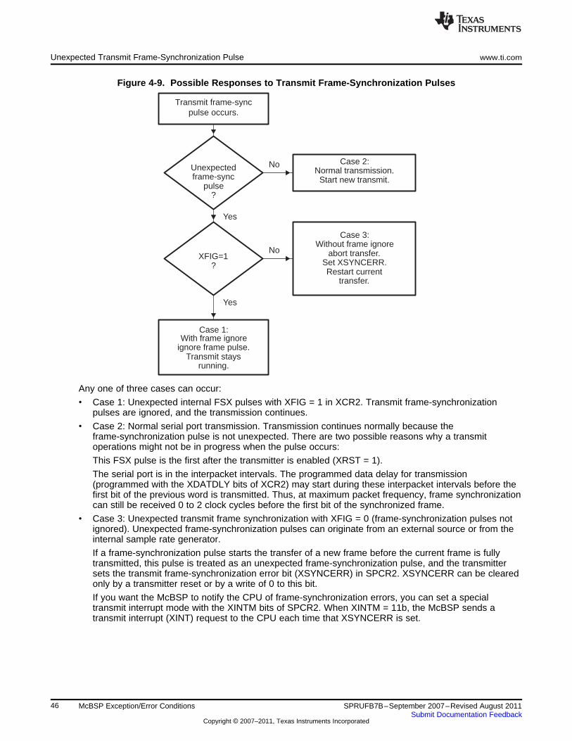
Yes
No
Yes
No
running.Transmit stays
ignore frame pulse.With frame ignore
Case 1:
transfer.Restart current
Set XSYNCERR.abort transfer.
Without frame ignoreCase 3:
Start new transmit.Normal transmission.
Case 2:
pulse occurs.Transmit frame-sync
?XFIG=1
?pulse
frame-syncUnexpected
Unexpected Transmit Frame-Synchronization Pulse www.ti.com
Figure 4-9. Possible Responses to Transmit Frame-Synchronization Pulses
Any one of three cases can occur:
• Case 1: Unexpected internal FSX pulses with XFIG = 1 in XCR2. Transmit frame-synchronizationpulses are ignored, and the transmission continues.
• Case 2: Normal serial port transmission. Transmission continues normally because theframe-synchronization pulse is not unexpected. There are two possible reasons why a transmitoperations might not be in progress when the pulse occurs:
This FSX pulse is the first after the transmitter is enabled (XRST = 1).
The serial port is in the interpacket intervals. The programmed data delay for transmission(programmed with the XDATDLY bits of XCR2) may start during these interpacket intervals before thefirst bit of the previous word is transmitted. Thus, at maximum packet frequency, frame synchronizationcan still be received 0 to 2 clock cycles before the first bit of the synchronized frame.
• Case 3: Unexpected transmit frame synchronization with XFIG = 0 (frame-synchronization pulses notignored). Unexpected frame-synchronization pulses can originate from an external source or from theinternal sample rate generator.
If a frame-synchronization pulse starts the transfer of a new frame before the current frame is fullytransmitted, this pulse is treated as an unexpected frame-synchronization pulse, and the transmittersets the transmit frame-synchronization error bit (XSYNCERR) in SPCR2. XSYNCERR can be clearedonly by a transmitter reset or by a write of 0 to this bit.
If you want the McBSP to notify the CPU of frame-synchronization errors, you can set a specialtransmit interrupt mode with the XINTM bits of SPCR2. When XINTM = 11b, the McBSP sends atransmit interrupt (XINT) request to the CPU each time that XSYNCERR is set.
46 McBSP Exception/Error Conditions SPRUFB7B–September 2007–Revised August 2011Submit Documentation Feedback
Copyright © 2007–2011, Texas Instruments Incorporated
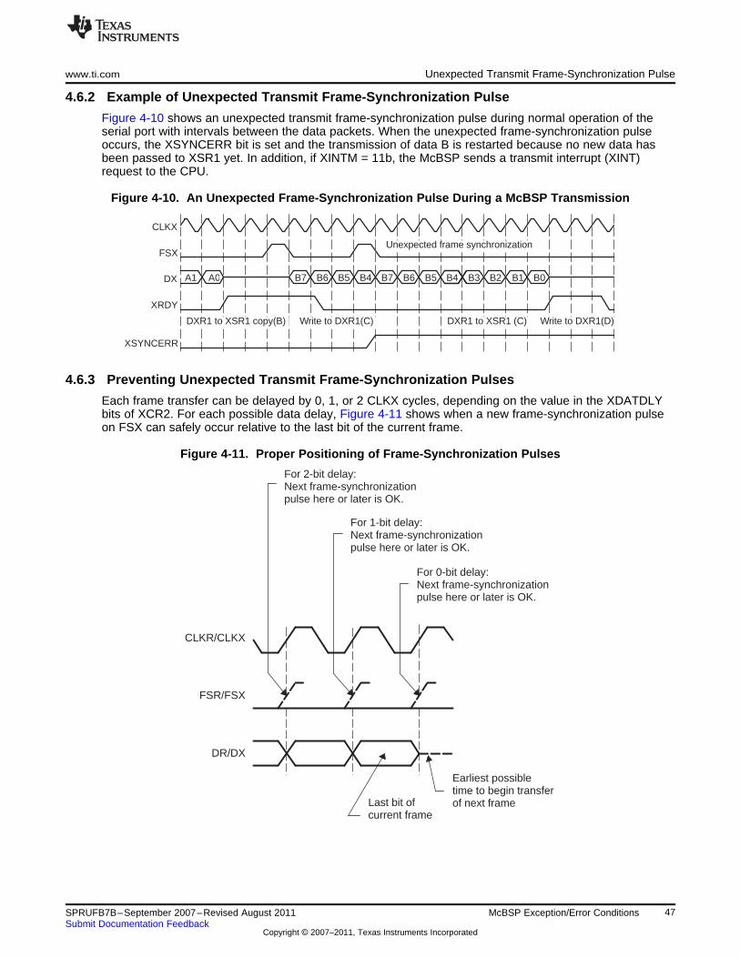
ÁÁÁB0B1B2B3B4B5B6B7B4B5B6B7A0A1
XSYNCERR
XRDY
DX
FSX
CLKX ÁÁÁÁÁÁWrite to DXR1(D)DXR1 to XSR1 (C)Write to DXR1(C)DXR1 to XSR1 copy(B)
Unexpected frame synchronization
For 2-bit delay:Next frame-synchronizationpulse here or later is OK.
For 1-bit delay:Next frame-synchronizationpulse here or later is OK.
For 0-bit delay:Next frame-synchronizationpulse here or later is OK.
CLKR/CLKX
FSR/FSX
DR/DX
Last bit ofcurrent frame
Earliest possibletime to begin transferof next frame
www.ti.com Unexpected Transmit Frame-Synchronization Pulse
4.6.2 Example of Unexpected Transmit Frame-Synchronization Pulse
Figure 4-10 shows an unexpected transmit frame-synchronization pulse during normal operation of theserial port with intervals between the data packets. When the unexpected frame-synchronization pulseoccurs, the XSYNCERR bit is set and the transmission of data B is restarted because no new data hasbeen passed to XSR1 yet. In addition, if XINTM = 11b, the McBSP sends a transmit interrupt (XINT)request to the CPU.
Figure 4-10. An Unexpected Frame-Synchronization Pulse During a McBSP Transmission
4.6.3 Preventing Unexpected Transmit Frame-Synchronization Pulses
Each frame transfer can be delayed by 0, 1, or 2 CLKX cycles, depending on the value in the XDATDLYbits of XCR2. For each possible data delay, Figure 4-11 shows when a new frame-synchronization pulseon FSX can safely occur relative to the last bit of the current frame.
Figure 4-11. Proper Positioning of Frame-Synchronization Pulses
47SPRUFB7B–September 2007–Revised August 2011 McBSP Exception/Error ConditionsSubmit Documentation Feedback
Copyright © 2007–2011, Texas Instruments Incorporated

48 McBSP Exception/Error Conditions SPRUFB7B–September 2007–Revised August 2011Submit Documentation Feedback
Copyright © 2007–2011, Texas Instruments Incorporated
Chapter 5SPRUFB7B–September 2007–Revised August 2011
Multichannel Selection Modes
This section discusses the multichannel selection modes for the McBSP.
Topic ........................................................................................................................... Page
5.1 Channels, Blocks, and Partitions ........................................................................ 505.2 Multichannel Selection ....................................................................................... 515.3 Configuring a Frame for Multichannel Selection .................................................... 515.4 Using Two Partitions ......................................................................................... 515.5 Using Eight Partitions ........................................................................................ 535.6 Receive Multichannel Selection Mode .................................................................. 545.7 Transmit Multichannel Selection Modes ............................................................... 545.8 Using Interrupts Between Block Transfers ........................................................... 56
49SPRUFB7B–September 2007–Revised August 2011 Multichannel Selection ModesSubmit Documentation Feedback
Copyright © 2007–2011, Texas Instruments Incorporated
Channels, Blocks, and Partitions www.ti.com
5.1 Channels, Blocks, and Partitions
A McBSP channel is a time slot for shifting in/out the bits of one serial word. Each McBSP supports up to128 channels for reception and 128 channels for transmission.
In the receiver and in the transmitter, the 128 available channels are divided into eight blocks that eachcontain 16 contiguous channels (see Table 5-1 through Table 5-3) :
• It is possible to have two receive partitions (A & B) and 8 transmit partitions (A – H).
• McBSP can transmit/receive on selected channels.
• Each channel partition has a dedicated channel-enable register. Each bit controls whether data flow isallowed or prevented in one of the channels assigned to that partition.
• There are three transmit multichannel modes and one receive multichannel mode.
Table 5-1. Block - Channel Assignment
Block Channels
0 0 -15
1 16 - 31
2 32 - 47
3 48 - 63
4 64 - 79
5 80 - 95
6 96 - 111
7 112 - 127
The blocks are assigned to partitions according to the selected partition mode. In the two-partitionmode (described in Section 5.4), you assign one even-numbered block (0, 2, 4, or 6) to partition A andone odd-numbered block (1, 3, 5, or 7) to partition B. In the 8-partition mode (described in Section 5.5),blocks 0 through 7 are automatically assigned to partitions, A through H, respectively.
Table 5-2. 2-Partition Mode
Partition Blocks
A 0 or 2 or 4 or 6
B 1 or 3 or 5 or 7
Table 5-3. 8-Partition mode
Partition Blocks Channels
A 0 0 -15
B 1 16 - 31
C 2 32 - 47
D 3 48 - 63
E 4 64 - 79
F 5 80 - 95
G 6 96 - 111
H 7 112 - 127
50 Multichannel Selection Modes SPRUFB7B–September 2007–Revised August 2011Submit Documentation Feedback
Copyright © 2007–2011, Texas Instruments Incorporated
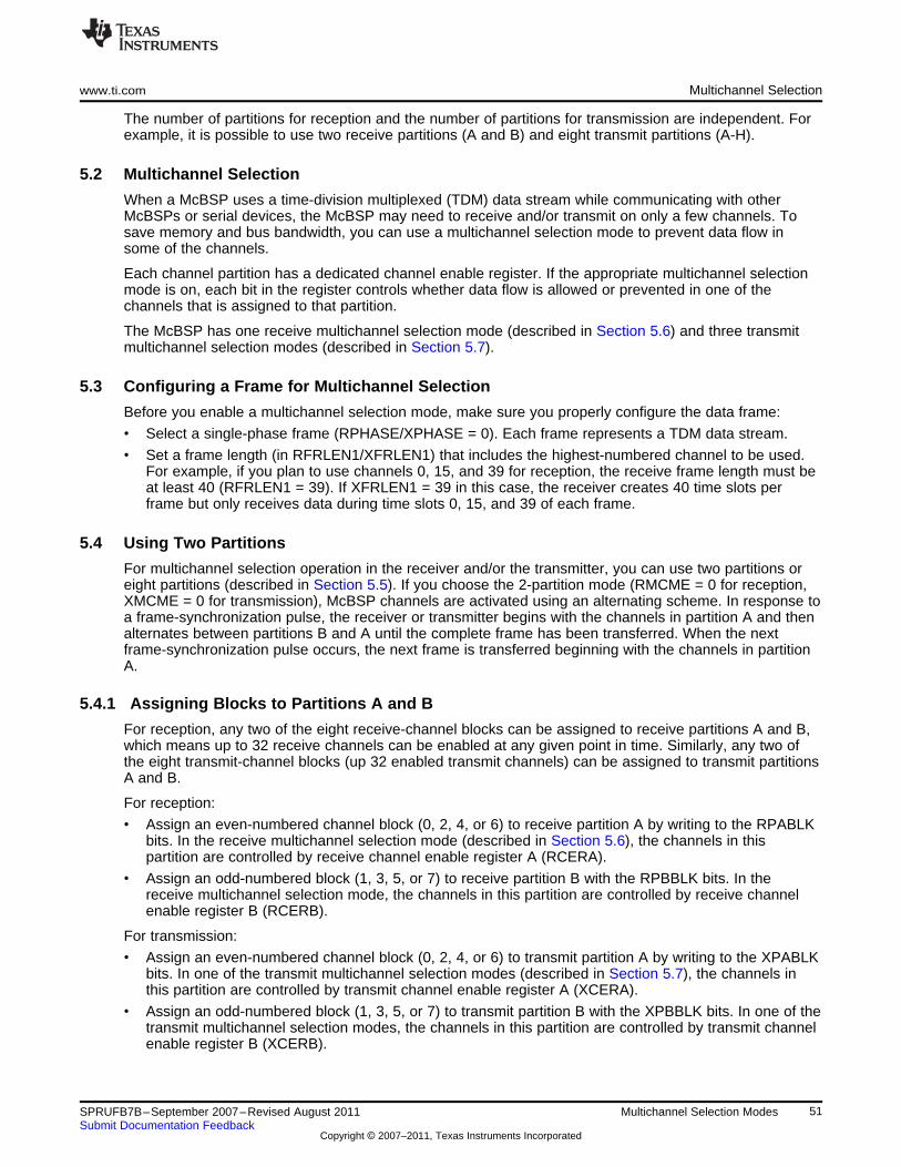
www.ti.com Multichannel Selection
The number of partitions for reception and the number of partitions for transmission are independent. Forexample, it is possible to use two receive partitions (A and B) and eight transmit partitions (A-H).
5.2 Multichannel Selection
When a McBSP uses a time-division multiplexed (TDM) data stream while communicating with otherMcBSPs or serial devices, the McBSP may need to receive and/or transmit on only a few channels. Tosave memory and bus bandwidth, you can use a multichannel selection mode to prevent data flow insome of the channels.
Each channel partition has a dedicated channel enable register. If the appropriate multichannel selectionmode is on, each bit in the register controls whether data flow is allowed or prevented in one of thechannels that is assigned to that partition.
The McBSP has one receive multichannel selection mode (described in Section 5.6) and three transmitmultichannel selection modes (described in Section 5.7).
5.3 Configuring a Frame for Multichannel Selection
Before you enable a multichannel selection mode, make sure you properly configure the data frame:
• Select a single-phase frame (RPHASE/XPHASE = 0). Each frame represents a TDM data stream.
• Set a frame length (in RFRLEN1/XFRLEN1) that includes the highest-numbered channel to be used.For example, if you plan to use channels 0, 15, and 39 for reception, the receive frame length must beat least 40 (RFRLEN1 = 39). If XFRLEN1 = 39 in this case, the receiver creates 40 time slots perframe but only receives data during time slots 0, 15, and 39 of each frame.
5.4 Using Two Partitions
For multichannel selection operation in the receiver and/or the transmitter, you can use two partitions oreight partitions (described in Section 5.5). If you choose the 2-partition mode (RMCME = 0 for reception,XMCME = 0 for transmission), McBSP channels are activated using an alternating scheme. In response toa frame-synchronization pulse, the receiver or transmitter begins with the channels in partition A and thenalternates between partitions B and A until the complete frame has been transferred. When the nextframe-synchronization pulse occurs, the next frame is transferred beginning with the channels in partitionA.
5.4.1 Assigning Blocks to Partitions A and B
For reception, any two of the eight receive-channel blocks can be assigned to receive partitions A and B,which means up to 32 receive channels can be enabled at any given point in time. Similarly, any two ofthe eight transmit-channel blocks (up 32 enabled transmit channels) can be assigned to transmit partitionsA and B.
For reception:
• Assign an even-numbered channel block (0, 2, 4, or 6) to receive partition A by writing to the RPABLKbits. In the receive multichannel selection mode (described in Section 5.6), the channels in thispartition are controlled by receive channel enable register A (RCERA).
• Assign an odd-numbered block (1, 3, 5, or 7) to receive partition B with the RPBBLK bits. In thereceive multichannel selection mode, the channels in this partition are controlled by receive channelenable register B (RCERB).
For transmission:
• Assign an even-numbered channel block (0, 2, 4, or 6) to transmit partition A by writing to the XPABLKbits. In one of the transmit multichannel selection modes (described in Section 5.7), the channels inthis partition are controlled by transmit channel enable register A (XCERA).
• Assign an odd-numbered block (1, 3, 5, or 7) to transmit partition B with the XPBBLK bits. In one of thetransmit multichannel selection modes, the channels in this partition are controlled by transmit channelenable register B (XCERB).
51SPRUFB7B–September 2007–Revised August 2011 Multichannel Selection ModesSubmit Documentation Feedback
Copyright © 2007–2011, Texas Instruments Incorporated
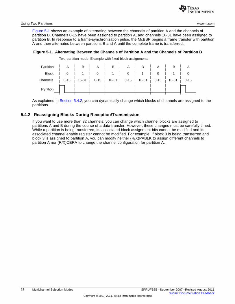
0-1516-310-1516-310-1516-310-1516-310-15
Block
Channels
FS(R/X)
ÁÁÁÁÁÁÁÁÁÁÁÁÁÁÁÁÁÁÁÁÁÁÁÁÁÁÁÁÁÁÁÁÁÁÁÁÁÁÁÁÁÁÁÁÁÁÁÁÁÁÁÁÁÁÁÁÁÁÁÁÁÁÁÁÁÁÁÁÁÁÁÁÁÁÁÁÁÁÁÁÁÁÁÁÁÁÁÁÁÁÁÁÁÁÁÁÁÁÁÁÁÁÁÁÁÁÁÁÁÁÁÁÁÁÁÁÁÁÁÁ0 1 0 1 0 1 0 1 0
Partition A B A B A B A B A
Two-partition mode. Example with fixed block assignments
Using Two Partitions www.ti.com
Figure 5-1 shows an example of alternating between the channels of partition A and the channels ofpartition B. Channels 0-15 have been assigned to partition A, and channels 16-31 have been assigned topartition B. In response to a frame-synchronization pulse, the McBSP begins a frame transfer with partitionA and then alternates between partitions B and A until the complete frame is transferred.
Figure 5-1. Alternating Between the Channels of Partition A and the Channels of Partition B
As explained in Section 5.4.2, you can dynamically change which blocks of channels are assigned to thepartitions.
5.4.2 Reassigning Blocks During Reception/Transmission
If you want to use more than 32 channels, you can change which channel blocks are assigned topartitions A and B during the course of a data transfer. However, these changes must be carefully timed.While a partition is being transferred, its associated block assignment bits cannot be modified and itsassociated channel enable register cannot be modified. For example, if block 3 is being transferred andblock 3 is assigned to partition A, you can modify neither (R/X)PABLK to assign different channels topartition A nor (R/X)CERA to change the channel configuration for partition A.
52 Multichannel Selection Modes SPRUFB7B–September 2007–Revised August 2011Submit Documentation Feedback
Copyright © 2007–2011, Texas Instruments Incorporated
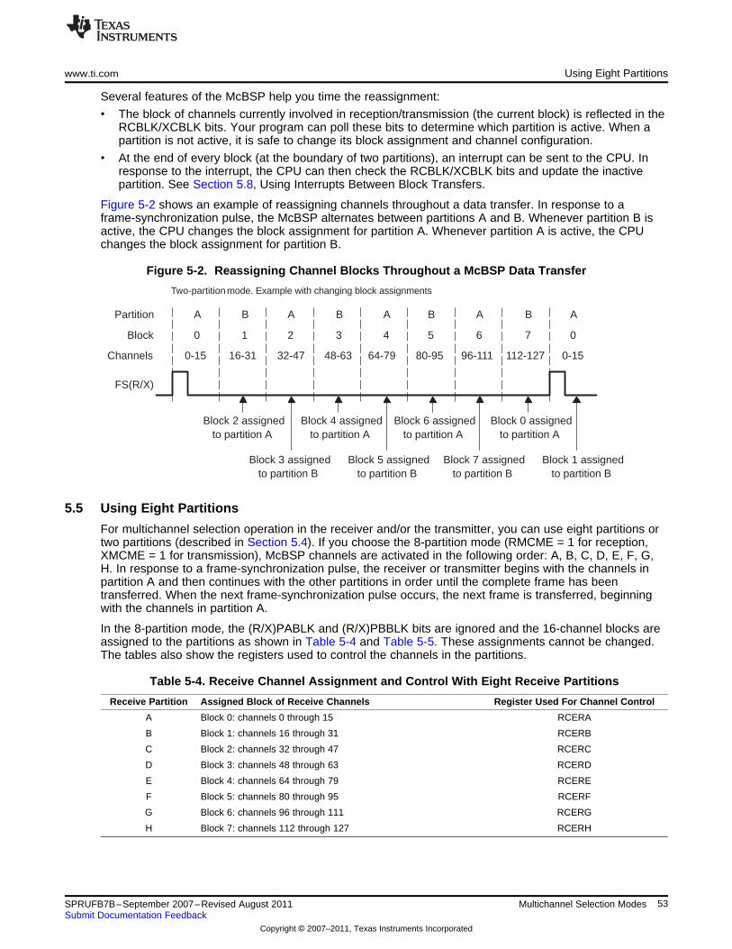
0-15112-12796-11180-9564-7948-6332-4716-310-15
Block
Channels
FS(R/X)
ÁÁÁÁÁÁÁÁÁÁÁÁÁÁÁÁÁÁÁÁÁÁÁÁÁÁÁÁÁÁÁÁÁÁÁÁÁÁÁÁÁÁÁÁÁÁÁÁÁÁÁÁÁÁÁÁÁÁÁÁÁÁÁÁÁÁÁÁÁÁÁÁÁÁÁÁÁÁÁÁÁÁÁÁÁÁÁÁÁÁÁÁÁÁÁÁÁÁÁÁ0 1 2 3 4 5 6 7 0
Partition A B A B A B A B A
Block 2 assignedto partition A
Block 4 assignedto partition A
Block 6 assignedto partition A
Block 0 assignedto partition A
Block 3 assignedto partition B
Block 5 assignedto partition B
Block 7 assignedto partition B
Block 1 assignedto partition B
Two-partition mode. Example with changing block assignments
www.ti.com Using Eight Partitions
Several features of the McBSP help you time the reassignment:
• The block of channels currently involved in reception/transmission (the current block) is reflected in theRCBLK/XCBLK bits. Your program can poll these bits to determine which partition is active. When apartition is not active, it is safe to change its block assignment and channel configuration.
• At the end of every block (at the boundary of two partitions), an interrupt can be sent to the CPU. Inresponse to the interrupt, the CPU can then check the RCBLK/XCBLK bits and update the inactivepartition. See Section 5.8, Using Interrupts Between Block Transfers.
Figure 5-2 shows an example of reassigning channels throughout a data transfer. In response to aframe-synchronization pulse, the McBSP alternates between partitions A and B. Whenever partition B isactive, the CPU changes the block assignment for partition A. Whenever partition A is active, the CPUchanges the block assignment for partition B.
Figure 5-2. Reassigning Channel Blocks Throughout a McBSP Data Transfer
5.5 Using Eight Partitions
For multichannel selection operation in the receiver and/or the transmitter, you can use eight partitions ortwo partitions (described in Section 5.4). If you choose the 8-partition mode (RMCME = 1 for reception,XMCME = 1 for transmission), McBSP channels are activated in the following order: A, B, C, D, E, F, G,H. In response to a frame-synchronization pulse, the receiver or transmitter begins with the channels inpartition A and then continues with the other partitions in order until the complete frame has beentransferred. When the next frame-synchronization pulse occurs, the next frame is transferred, beginningwith the channels in partition A.
In the 8-partition mode, the (R/X)PABLK and (R/X)PBBLK bits are ignored and the 16-channel blocks areassigned to the partitions as shown in Table 5-4 and Table 5-5. These assignments cannot be changed.The tables also show the registers used to control the channels in the partitions.
Table 5-4. Receive Channel Assignment and Control With Eight Receive Partitions
Receive Partition Assigned Block of Receive Channels Register Used For Channel Control
A Block 0: channels 0 through 15 RCERA
B Block 1: channels 16 through 31 RCERB
C Block 2: channels 32 through 47 RCERC
D Block 3: channels 48 through 63 RCERD
E Block 4: channels 64 through 79 RCERE
F Block 5: channels 80 through 95 RCERF
G Block 6: channels 96 through 111 RCERG
H Block 7: channels 112 through 127 RCERH
53SPRUFB7B–September 2007–Revised August 2011 Multichannel Selection ModesSubmit Documentation Feedback
Copyright © 2007–2011, Texas Instruments Incorporated
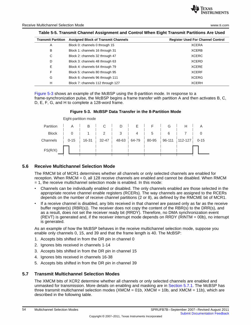
0-15112-12796-11180-9564-7948-6332-4716-310-15
Block
Channels
FS(R/X)
ÁÁÁÁÁÁÁÁÁÁÁÁÁÁÁÁÁÁÁÁÁÁÁÁÁÁÁÁÁÁÁÁÁÁÁÁÁÁÁÁÁÁÁÁÁÁÁÁÁÁÁÁÁÁÁÁÁÁÁÁÁÁÁÁÁÁÁÁÁÁÁÁÁÁÁÁÁÁÁÁÁÁÁÁÁÁÁÁÁÁÁÁÁÁÁÁÁÁÁÁ0 1 2 3 4 5 6 7 0
Partition A B C D E F G H A
Eight-partition mode
Receive Multichannel Selection Mode www.ti.com
Table 5-5. Transmit Channel Assignment and Control When Eight Transmit Partitions Are Used
Transmit Partition Assigned Block of Transmit Channels Register Used For Channel Control
A Block 0: channels 0 through 15 XCERA
B Block 1: channels 16 through 31 XCERB
C Block 2: channels 32 through 47 XCERC
D Block 3: channels 48 through 63 XCERD
E Block 4: channels 64 through 79 XCERE
F Block 5: channels 80 through 95 XCERF
G Block 6: channels 96 through 111 XCERG
H Block 7: channels 112 through 127 XCERH
Figure 5-3 shows an example of the McBSP using the 8-partition mode. In response to aframe-synchronization pulse, the McBSP begins a frame transfer with partition A and then activates B, C,D, E, F, G, and H to complete a 128-word frame.
Figure 5-3. McBSP Data Transfer in the 8-Partition Mode
5.6 Receive Multichannel Selection Mode
The RMCM bit of MCR1 determines whether all channels or only selected channels are enabled forreception. When RMCM = 0, all 128 receive channels are enabled and cannot be disabled. When RMCM= 1, the receive multichannel selection mode is enabled. In this mode:
• Channels can be individually enabled or disabled. The only channels enabled are those selected in theappropriate receive channel enable registers (RCERs). The way channels are assigned to the RCERsdepends on the number of receive channel partitions (2 or 8), as defined by the RMCME bit of MCR1.
• If a receive channel is disabled, any bits received in that channel are passed only as far as the receivebuffer register(s) (RBR(s)). The receiver does not copy the content of the RBR(s) to the DRR(s), andas a result, does not set the receiver ready bit (RRDY). Therefore, no DMA synchronization event(REVT) is generated and, if the receiver interrupt mode depends on RRDY (RINTM = 00b), no interruptis generated.
As an example of how the McBSP behaves in the receive multichannel selection mode, suppose youenable only channels 0, 15, and 39 and that the frame length is 40. The McBSP:
1. Accepts bits shifted in from the DR pin in channel 0
2. Ignores bits received in channels 1-14
3. Accepts bits shifted in from the DR pin in channel 15
4. Ignores bits received in channels 16-38
5. Accepts bits shifted in from the DR pin in channel 39
5.7 Transmit Multichannel Selection Modes
The XMCM bits of XCR2 determine whether all channels or only selected channels are enabled andunmasked for transmission. More details on enabling and masking are in Section 5.7.1. The McBSP hasthree transmit multichannel selection modes (XMCM = 01b, XMCM = 10b, and XMCM = 11b), which aredescribed in the following table.
54 Multichannel Selection Modes SPRUFB7B–September 2007–Revised August 2011Submit Documentation Feedback
Copyright © 2007–2011, Texas Instruments Incorporated
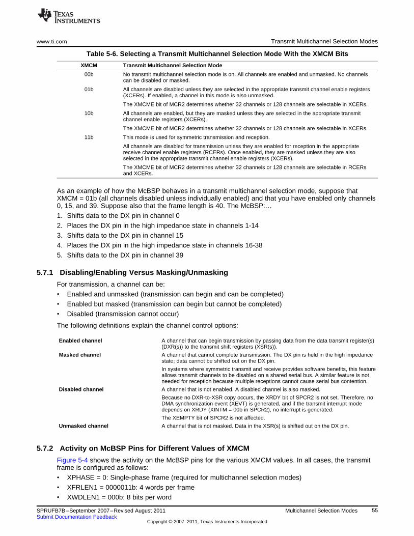
www.ti.com Transmit Multichannel Selection Modes
Table 5-6. Selecting a Transmit Multichannel Selection Mode With the XMCM Bits
XMCM Transmit Multichannel Selection Mode
00b No transmit multichannel selection mode is on. All channels are enabled and unmasked. No channelscan be disabled or masked.
01b All channels are disabled unless they are selected in the appropriate transmit channel enable registers(XCERs). If enabled, a channel in this mode is also unmasked.
The XMCME bit of MCR2 determines whether 32 channels or 128 channels are selectable in XCERs.
10b All channels are enabled, but they are masked unless they are selected in the appropriate transmitchannel enable registers (XCERs).
The XMCME bit of MCR2 determines whether 32 channels or 128 channels are selectable in XCERs.
11b This mode is used for symmetric transmission and reception.
All channels are disabled for transmission unless they are enabled for reception in the appropriatereceive channel enable registers (RCERs). Once enabled, they are masked unless they are alsoselected in the appropriate transmit channel enable registers (XCERs).
The XMCME bit of MCR2 determines whether 32 channels or 128 channels are selectable in RCERsand XCERs.
As an example of how the McBSP behaves in a transmit multichannel selection mode, suppose thatXMCM = 01b (all channels disabled unless individually enabled) and that you have enabled only channels0, 15, and 39. Suppose also that the frame length is 40. The McBSP:…1. Shifts data to the DX pin in channel 0
2. Places the DX pin in the high impedance state in channels 1-14
3. Shifts data to the DX pin in channel 15
4. Places the DX pin in the high impedance state in channels 16-38
5. Shifts data to the DX pin in channel 39
5.7.1 Disabling/Enabling Versus Masking/Unmasking
For transmission, a channel can be:
• Enabled and unmasked (transmission can begin and can be completed)
• Enabled but masked (transmission can begin but cannot be completed)
• Disabled (transmission cannot occur)
The following definitions explain the channel control options:
Enabled channel A channel that can begin transmission by passing data from the data transmit register(s)(DXR(s)) to the transmit shift registers (XSR(s)).
Masked channel A channel that cannot complete transmission. The DX pin is held in the high impedancestate; data cannot be shifted out on the DX pin.
In systems where symmetric transmit and receive provides software benefits, this featureallows transmit channels to be disabled on a shared serial bus. A similar feature is notneeded for reception because multiple receptions cannot cause serial bus contention.
Disabled channel A channel that is not enabled. A disabled channel is also masked.
Because no DXR-to-XSR copy occurs, the XRDY bit of SPCR2 is not set. Therefore, noDMA synchronization event (XEVT) is generated, and if the transmit interrupt modedepends on XRDY (XINTM = 00b in SPCR2), no interrupt is generated.
The XEMPTY bit of SPCR2 is not affected.
Unmasked channel A channel that is not masked. Data in the XSR(s) is shifted out on the DX pin.
5.7.2 Activity on McBSP Pins for Different Values of XMCM
Figure 5-4 shows the activity on the McBSP pins for the various XMCM values. In all cases, the transmitframe is configured as follows:
• XPHASE = 0: Single-phase frame (required for multichannel selection modes)
• XFRLEN1 = 0000011b: 4 words per frame
• XWDLEN1 = 000b: 8 bits per word
55SPRUFB7B–September 2007–Revised August 2011 Multichannel Selection ModesSubmit Documentation Feedback
Copyright © 2007–2011, Texas Instruments Incorporated
Using Interrupts Between Block Transfers www.ti.com
• XMCME = 0: 2-partition mode (only partitions A and B used)
In the case where XMCM = 11b, transmission and reception are symmetric, which means thecorresponding bits for the receiver (RPHASE, RFRLEN1, RWDLEN1, and RMCME) must have the samevalues as XPHASE, XFRLEN1, and XWDLEN1, respectively.
In the figure, the arrows showing where the various events occur are only sample indications. Whereverpossible, there is a time window in which these events can occur.
5.8 Using Interrupts Between Block Transfers
When a multichannel selection mode is used, an interrupt request can be sent to the CPU at the end ofevery 16-channel block (at the boundary between partitions and at the end of the frame). In the receivemultichannel selection mode, a receive interrupt (RINT) request is generated at the end of each blocktransfer if RINTM = 01b. In any of the transmit multichannel selection modes, a transmit interrupt (XINT)request is generated at the end of each block transfer if XINTM = 01b. When RINTM/XINTM = 01b, nointerrupt is generated unless a multichannel selection mode is on.
These interrupt pulses are active high and last for two CPU clock cycles.
This type of interrupt is especially helpful if you are using the two-partition mode (described in Section 5.4)and you want to know when you can assign a different block of channels to partition A or B.
56 Multichannel Selection Modes SPRUFB7B–September 2007–Revised August 2011Submit Documentation Feedback
Copyright © 2007–2011, Texas Instruments Incorporated
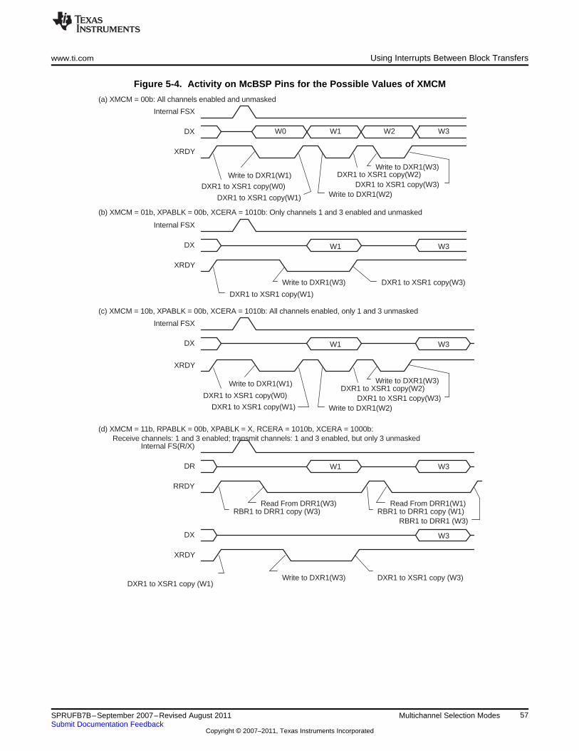
DXR1 to XSR1 copy (W1)
XRDY
DXR1 to XSR1 copy (W3)Write to DXR1(W3)
ÁÁÁÁÁÁÁÁ W3
ÁÁÁÁDX
RBR1 to DRR1 (W3)
Read From DRR1(W1)RBR1 to DRR1 copy (W1)RBR1 to DRR1 copy (W3)
Read From DRR1(W3)
ÁÁÁÁÁÁÁW3
ÁÁÁ(d) XMCM = 11b, RPABLK = 00b, XPABLK = X, RCERA = 1010b, XCERA = 1000b: Receive channels: 1 and 3 enabled; transmit channels: 1 and 3 enabled, but only 3 unmaskedÁÁÁW1
ÁÁÁÁÁÁInternal FS(R/X)
DR
RRDY
Write to DXR1(W3)
DXR1 to XSR1 copy(W0)
Write to DXR1(W1)
DXR1 to XSR1 copy(W1) Write to DXR1(W2)
XRDY
DXR1 to XSR1 copy(W3)DXR1 to XSR1 copy(W2)
W3
(c) XMCM = 10b, XPABLK = 00b, XCERA = 1010b: All channels enabled, only 1 and 3 unmasked
Internal FSX
ÁÁÁÁÁÁÁÁW1
ÁÁÁÁÁÁÁÁÁÁÁÁDX
(b) XMCM = 01b, XPABLK = 00b, XCERA = 1010b: Only channels 1 and 3 enabled and unmasked
DXR1 to XSR1 copy(W3)Write to DXR1(W3)
XRDY
DXR1 to XSR1 copy(W1)
W3
ÁÁÁÁÁÁÁÁÁÁÁÁDX
ÁÁÁÁÁÁÁÁ W1
Internal FSX
(a) XMCM = 00b: All channels enabled and unmasked
W3W2W1W0
XRDY
DX
Internal FSX
DXR1 to XSR1 copy(W0)Write to DXR1(W1)
DXR1 to XSR1 copy(W1) Write to DXR1(W2)DXR1 to XSR1 copy(W3)
DXR1 to XSR1 copy(W2)Write to DXR1(W3)
ÁÁÁÁÁÁ ÁÁÁwww.ti.com Using Interrupts Between Block Transfers
Figure 5-4. Activity on McBSP Pins for the Possible Values of XMCM
57SPRUFB7B–September 2007–Revised August 2011 Multichannel Selection ModesSubmit Documentation Feedback
Copyright © 2007–2011, Texas Instruments Incorporated

58 Multichannel Selection Modes SPRUFB7B–September 2007–Revised August 2011Submit Documentation Feedback
Copyright © 2007–2011, Texas Instruments Incorporated
Chapter 6SPRUFB7B–September 2007–Revised August 2011
SPI Operation Using the Clock Stop Mode
This chapter explains how to use the McBSP in SPI mode.
Topic ........................................................................................................................... Page
6.1 SPI Protocol ..................................................................................................... 606.2 Clock Stop Mode ............................................................................................... 606.3 Bits Used to Enable and Configure the Clock Stop Mode ....................................... 606.4 Clock Stop Mode Timing Diagrams ...................................................................... 616.5 Procedure for Configuring a McBSP for SPI Operation .......................................... 636.6 McBSP as the SPI Master ................................................................................... 636.7 McBSP as an SPI Slave ...................................................................................... 65
59SPRUFB7B–September 2007–Revised August 2011 SPI Operation Using the Clock Stop ModeSubmit Documentation Feedback
Copyright © 2007–2011, Texas Instruments Incorporated
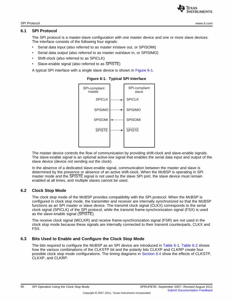
SPI-compliant
SPICLK
SPISIMO
SPISOMI
SPISTE
SPI-compliantslave
SPICLK
SPISIMO
SPISOMI
SPISTE
master
SPI Protocol www.ti.com
6.1 SPI Protocol
The SPI protocol is a master-slave configuration with one master device and one or more slave devices.The interface consists of the following four signals:
• Serial data input (also referred to as master in/slave out, or SPISOMI)
• Serial data output (also referred to as master out/slave in, or SPISIMO)
• Shift-clock (also referred to as SPICLK)
• Slave-enable signal (also referred to as SPISTE)
A typical SPI interface with a single slave device is shown in Figure 6-1.
Figure 6-1. Typical SPI Interface
The master device controls the flow of communication by providing shift-clock and slave-enable signals.The slave-enable signal is an optional active-low signal that enables the serial data input and output of theslave device (device not sending out the clock).
In the absence of a dedicated slave-enable signal, communication between the master and slave isdetermined by the presence or absence of an active shift-clock. When the McBSP is operating in SPImaster mode and the SPISTE signal is not used by the slave SPI port, the slave device must remainenabled at all times, and multiple slaves cannot be used.
6.2 Clock Stop Mode
The clock stop mode of the McBSP provides compatibility with the SPI protocol. When the McBSP isconfigured in clock stop mode, the transmitter and receiver are internally synchronized so that the McBSPfunctions as an SPI master or slave device. The transmit clock signal (CLKX) corresponds to the serialclock signal (SPICLK) of the SPI protocol, while the transmit frame-synchronization signal (FSX) is usedas the slave-enable signal (SPISTE).
The receive clock signal (MCLKR) and receive frame-synchronization signal (FSR) are not used in theclock stop mode because these signals are internally connected to their transmit counterparts, CLKX andFSX.
6.3 Bits Used to Enable and Configure the Clock Stop Mode
The bits required to configure the McBSP as an SPI device are introduced in Table 6-1. Table 6-2 showshow the various combinations of the CLKSTP bit and the polarity bits CLKXP and CLKRP create fourpossible clock stop mode configurations. The timing diagrams in Section 6.4 show the effects of CLKSTP,CLKXP, and CLKRP.
60 SPI Operation Using the Clock Stop Mode SPRUFB7B–September 2007–Revised August 2011Submit Documentation Feedback
Copyright © 2007–2011, Texas Instruments Incorporated
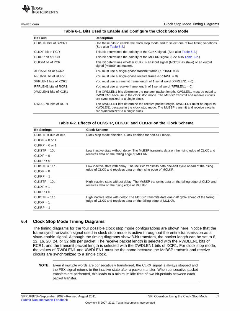
www.ti.com Clock Stop Mode Timing Diagrams
Table 6-1. Bits Used to Enable and Configure the Clock Stop Mode
Bit Field Description
CLKSTP bits of SPCR1 Use these bits to enable the clock stop mode and to select one of two timing variations.(See also Table 6-2.)
CLKXP bit of PCR This bit determines the polarity of the CLKX signal. (See also Table 6-2.)
CLKRP bit of PCR This bit determines the polarity of the MCLKR signal. (See also Table 6-2.)
CLKXM bit of PCR This bit determines whether CLKX is an input signal (McBSP as slave) or an outputsignal (McBSP as master).
XPHASE bit of XCR2 You must use a single-phase transmit frame (XPHASE = 0).
RPHASE bit of RCR2 You must use a single-phase receive frame (RPHASE = 0).
XFRLEN1 bits of XCR1 You must use a transmit frame length of 1 serial word (XFRLEN1 = 0).
RFRLEN1 bits of RCR1 You must use a receive frame length of 1 serial word (RFRLEN1 = 0).
XWDLEN1 bits of XCR1 The XWDLEN1 bits determine the transmit packet length. XWDLEN1 must be equal toRWDLEN1 because in the clock stop mode. The McBSP transmit and receive circuitsare synchronized to a single clock.
RWDLEN1 bits of RCR1 The RWDLEN1 bits determine the receive packet length. RWDLEN1 must be equal toXWDLEN1 because in the clock stop mode. The McBSP transmit and receive circuitsare synchronized to a single clock.
Table 6-2. Effects of CLKSTP, CLKXP, and CLKRP on the Clock Scheme
Bit Settings Clock Scheme
CLKSTP = 00b or 01b Clock stop mode disabled. Clock enabled for non-SPI mode.
CLKXP = 0 or 1
CLKRP = 0 or 1
CLKSTP = 10b Low inactive state without delay: The McBSP transmits data on the rising edge of CLKX andreceives data on the falling edge of MCLKR.CLKXP = 0
CLKRP = 0
CLKSTP = 11b Low inactive state with delay: The McBSP transmits data one-half cycle ahead of the risingedge of CLKX and receives data on the rising edge of MCLKR.CLKXP = 0
CLKRP = 1
CLKSTP = 10b High inactive state without delay: The McBSP transmits data on the falling edge of CLKX andreceives data on the rising edge of MCLKR.CLKXP = 1
CLKRP = 0
CLKSTP = 11b High inactive state with delay: The McBSP transmits data one-half cycle ahead of the fallingedge of CLKX and receives data on the falling edge of MCLKR.CLKXP = 1
CLKRP = 1
6.4 Clock Stop Mode Timing Diagrams
The timing diagrams for the four possible clock stop mode configurations are shown here. Notice that theframe-synchronization signal used in clock stop mode is active throughout the entire transmission as aslave-enable signal. Although the timing diagrams show 8-bit transfers, the packet length can be set to 8,12, 16, 20, 24, or 32 bits per packet. The receive packet length is selected with the RWDLEN1 bits ofRCR1, and the transmit packet length is selected with the XWDLEN1 bits of XCR1. For clock stop mode,the values of RWDLEN1 and XWDLEN1 must be the same because the McBSP transmit and receivecircuits are synchronized to a single clock.
NOTE: Even if multiple words are consecutively transferred, the CLKX signal is always stopped andthe FSX signal returns to the inactive state after a packet transfer. When consecutive packettransfers are performed, this leads to a minimum idle time of two bit-periods between eachpacket transfer.
61SPRUFB7B–September 2007–Revised August 2011 SPI Operation Using the Clock Stop ModeSubmit Documentation Feedback
Copyright © 2007–2011, Texas Instruments Incorporated
B1B2B4 B3 B0B5B6B7
B0B1B2B3B4B5B6B7
FSX/SPISTE
DX or DR/SIMO
(from master)
CLKX/SPICLK
DX or DR/SOMI
(from slave)
B1B2B4 B3 B0B5B6B7
B0B1B2B3B4B5B6B7
FSX/SPISTE
DX or DR/SIMO
(from master)
CLKX/SPICLK
DX or DR/SOMI
(from slave)
B1B2B4 B3 B0B5B6B7
B0B1B2B3B4B5B6B7
FSX/SPISTE
CLKX/SPICLK
DX or DR/SIMO
(from master)
DX or DR/SOMI
(from slave)
B1B2B4 B3 B0B5B6B7
B0B1B2B3B4B5B6B7
FSX/SPISTE
CLKX/SPICLK
DX or DR/SIMO
(from master)
DX or DR/SOMI
(from slave)
Clock Stop Mode Timing Diagrams www.ti.com
Figure 6-2. SPI Transfer With CLKSTP = 10b (No Clock Delay), CLKXP = 0, and CLKRP = 0
A If the McBSP is the SPI master (CLKXM = 1), SIMO = DX. If the McBSP is the SPI slave (CLKXM = 0), SIMO = DR.
B If the McBSP is the SPI master (CLKXM = 1), SOMI = DR. If the McBSP is the SPI slave (CLKXM = 0), SOMI = DX.
Figure 6-3. SPI Transfer With CLKSTP = 11b (Clock Delay), CLKXP = 0, CLKRP = 1
A If the McBSP is the SPI master (CLKXM = 1), SIMO = DX. If the McBSP is the SPI slave (CLKXM = 0), SIMO = DR.
B If the McBSP is the SPI master (CLKXM = 1), SOMI = DR. If the McBSP is the SPI slave (CLKXM = 0), SOMI = DX.
Figure 6-4. SPI Transfer With CLKSTP = 10b (No Clock Delay), CLKXP = 1, and CLKRP = 0
A If the McBSP is the SPI master (CLKXM = 1), SIMO = DX. If the McBSP is the SPI slave (CLKXM = 0), SIMO = DR.
B If the McBSP is the SPI master (CLKXM = 1), SOMI = DR. If the McBSP is the SPI slave (CLKXM = 0), SOMI = DX.
Figure 6-5. SPI Transfer With CLKSTP = 11b (Clock Delay), CLKXP = 1, CLKRP = 1
A If the McBSP is the SPI master (CLKXM = 1), SIMO=DX. If the McBSP is the SPI slave (CLKXM = 0), SIMO = DR.
B If the McBSP is the SPI master (CLKXM = 1), SOMI=DR. If the McBSP is the SPI slave (CLKXM = 0), SOMI = DX.
62 SPI Operation Using the Clock Stop Mode SPRUFB7B–September 2007–Revised August 2011Submit Documentation Feedback
Copyright © 2007–2011, Texas Instruments Incorporated
www.ti.com Procedure for Configuring a McBSP for SPI Operation
6.5 Procedure for Configuring a McBSP for SPI Operation
To configure the McBSP for SPI master or slave operation:
Step 1. Place the transmitter and receiver in reset.
Clear the transmitter reset bit (XRST = 0) in SPCR2 to reset the transmitter. Clear the receiver reset bit(RRST = 0) in SPCR1 to reset the receiver.
Step 2. Place the sample rate generator in reset.
Clear the sample rate generator reset bit (GRST = 0) in SPCR2 to reset the sample rate generator.
Step 3. Program registers that affect SPI operation.
Program the appropriate McBSP registers to configure the McBSP for proper operation as an SPImaster or an SPI slave. For a list of important bits settings, see one of the following topics:
• McBSP as the SPI Master ( Section 6.6)
• McBSP as an SPI Slave ( Section 6.7)
Step 4. Enable the sample rate generator.
To release the sample rate generator from reset, set the sample rate generator reset bit (GRST = 1) inSPCR2.
Make sure that during the write to SPCR2, you only modify GRST. Otherwise, you modify the McBSPconfiguration you selected in the previous step.
Step 5. Enable the transmitter and receiver.
After the sample rate generator is released from reset, wait two sample rate generator clock periods forthe McBSP logic to stabilize.
If the CPU services the McBSP transmit and receive buffers, then you can immediately enable thetransmitter (XRST = 1 in SPCR2) and enable the receiver (RRST = 1 in SPCR1).
If the DMA controller services the McBSP transmit and receive buffers, then you must first configurethe DMA controller (this includes enabling the channels that service the McBSP buffers). When theDMA controller is ready, make XRST = 1 and RRST = 1.
In either case, make sure you only change XRST and RRST when you write to SPCR2 and SPCR1.Otherwise, you modify the bit settings you selected earlier in this procedure.
After the transmitter and receiver are released from reset, wait two sample rate generator clock periodsfor the McBSP logic to stabilize.
Step 6. If necessary, enable the frame-synchronization logic of the sample rate generator.
After the required data acquisition setup is done (DXR[1,2] is loaded with data), set FRST = 1 if aninternally generated frame-synchronization pulse is required (that is, if the McBSP is the SPI master).
6.6 McBSP as the SPI Master
An SPI interface with the McBSP used as the master is shown in Figure 6-6. When the McBSP isconfigured as a master, the transmit output signal (DX) is used as the SPISIMO signal of the SPI protocoland the receive input signal (DR) is used as the SPISOMI signal.
The register bit values required to configure the McBSP as a master are listed in Table 6-3. After the tableare more details about the configuration requirements.
63SPRUFB7B–September 2007–Revised August 2011 SPI Operation Using the Clock Stop ModeSubmit Documentation Feedback
Copyright © 2007–2011, Texas Instruments Incorporated
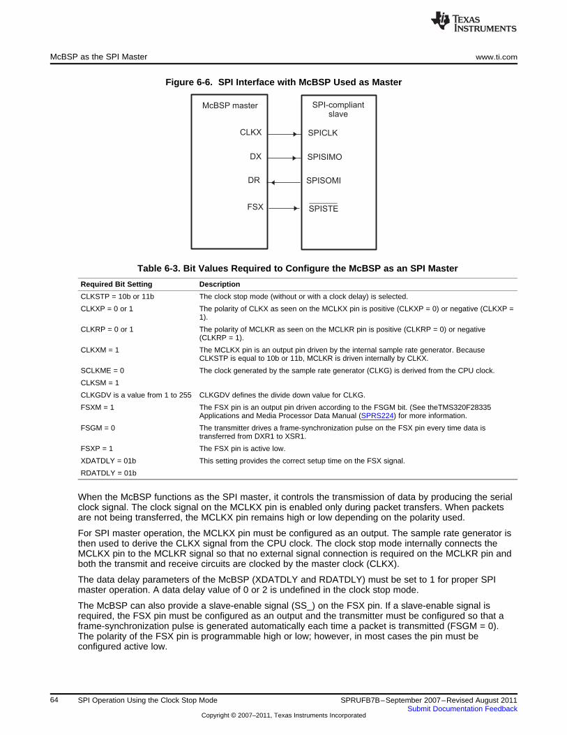
McBSP master
CLKX
DX
DR
FSX
SPI-compliantslave
SPICLK
SPISIMO
SPISOMI
SPISTE
McBSP as the SPI Master www.ti.com
Figure 6-6. SPI Interface with McBSP Used as Master
Table 6-3. Bit Values Required to Configure the McBSP as an SPI Master
Required Bit Setting Description
CLKSTP = 10b or 11b The clock stop mode (without or with a clock delay) is selected.
CLKXP = 0 or 1 The polarity of CLKX as seen on the MCLKX pin is positive (CLKXP = 0) or negative (CLKXP =1).
CLKRP = 0 or 1 The polarity of MCLKR as seen on the MCLKR pin is positive (CLKRP = 0) or negative(CLKRP = 1).
CLKXM = 1 The MCLKX pin is an output pin driven by the internal sample rate generator. BecauseCLKSTP is equal to 10b or 11b, MCLKR is driven internally by CLKX.
SCLKME = 0 The clock generated by the sample rate generator (CLKG) is derived from the CPU clock.
CLKSM = 1
CLKGDV is a value from 1 to 255 CLKGDV defines the divide down value for CLKG.
FSXM = 1 The FSX pin is an output pin driven according to the FSGM bit. (See theTMS320F28335Applications and Media Processor Data Manual (SPRS224) for more information.
FSGM = 0 The transmitter drives a frame-synchronization pulse on the FSX pin every time data istransferred from DXR1 to XSR1.
FSXP = 1 The FSX pin is active low.
XDATDLY = 01b This setting provides the correct setup time on the FSX signal.
RDATDLY = 01b
When the McBSP functions as the SPI master, it controls the transmission of data by producing the serialclock signal. The clock signal on the MCLKX pin is enabled only during packet transfers. When packetsare not being transferred, the MCLKX pin remains high or low depending on the polarity used.
For SPI master operation, the MCLKX pin must be configured as an output. The sample rate generator isthen used to derive the CLKX signal from the CPU clock. The clock stop mode internally connects theMCLKX pin to the MCLKR signal so that no external signal connection is required on the MCLKR pin andboth the transmit and receive circuits are clocked by the master clock (CLKX).
The data delay parameters of the McBSP (XDATDLY and RDATDLY) must be set to 1 for proper SPImaster operation. A data delay value of 0 or 2 is undefined in the clock stop mode.
The McBSP can also provide a slave-enable signal (SS_) on the FSX pin. If a slave-enable signal isrequired, the FSX pin must be configured as an output and the transmitter must be configured so that aframe-synchronization pulse is generated automatically each time a packet is transmitted (FSGM = 0).The polarity of the FSX pin is programmable high or low; however, in most cases the pin must beconfigured active low.
64 SPI Operation Using the Clock Stop Mode SPRUFB7B–September 2007–Revised August 2011Submit Documentation Feedback
Copyright © 2007–2011, Texas Instruments Incorporated
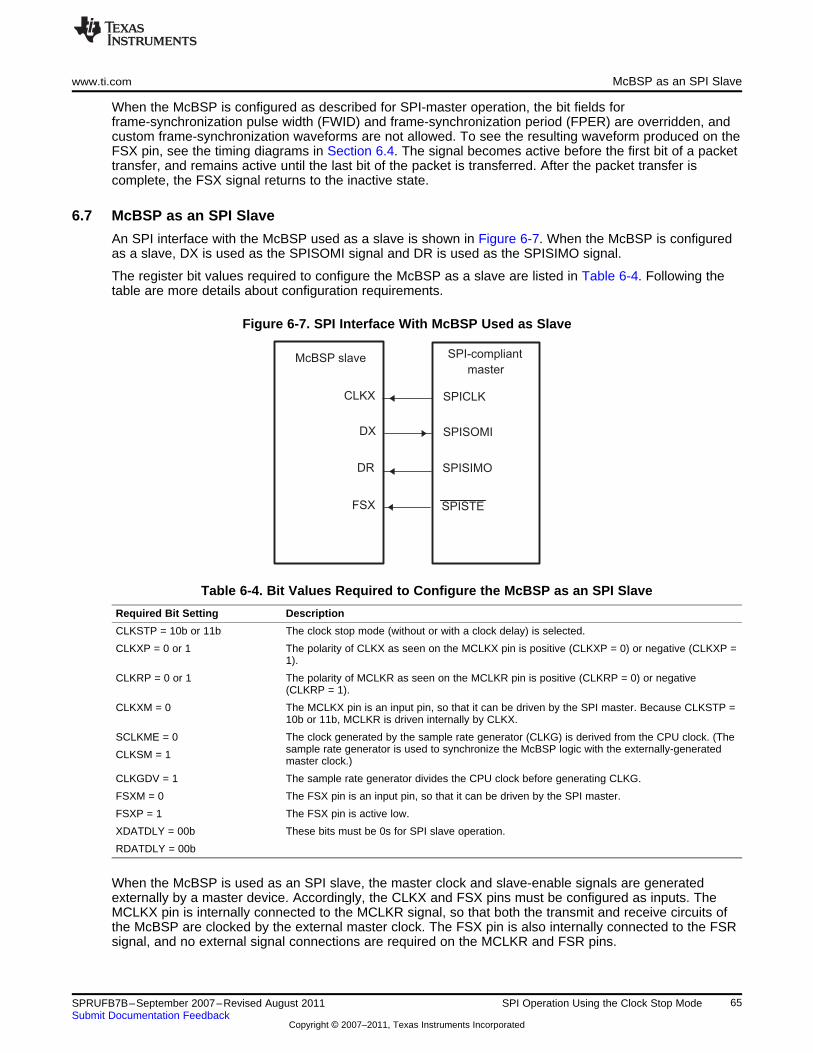
McBSP slave
CLKX
DX
DR
FSX
SPI-compliant
master
SPICLK
SPISOMI
SPISIMO
SPISTE
www.ti.com McBSP as an SPI Slave
When the McBSP is configured as described for SPI-master operation, the bit fields forframe-synchronization pulse width (FWID) and frame-synchronization period (FPER) are overridden, andcustom frame-synchronization waveforms are not allowed. To see the resulting waveform produced on theFSX pin, see the timing diagrams in Section 6.4. The signal becomes active before the first bit of a packettransfer, and remains active until the last bit of the packet is transferred. After the packet transfer iscomplete, the FSX signal returns to the inactive state.
6.7 McBSP as an SPI Slave
An SPI interface with the McBSP used as a slave is shown in Figure 6-7. When the McBSP is configuredas a slave, DX is used as the SPISOMI signal and DR is used as the SPISIMO signal.
The register bit values required to configure the McBSP as a slave are listed in Table 6-4. Following thetable are more details about configuration requirements.
Figure 6-7. SPI Interface With McBSP Used as Slave
Table 6-4. Bit Values Required to Configure the McBSP as an SPI Slave
Required Bit Setting Description
CLKSTP = 10b or 11b The clock stop mode (without or with a clock delay) is selected.
CLKXP = 0 or 1 The polarity of CLKX as seen on the MCLKX pin is positive (CLKXP = 0) or negative (CLKXP =1).
CLKRP = 0 or 1 The polarity of MCLKR as seen on the MCLKR pin is positive (CLKRP = 0) or negative(CLKRP = 1).
CLKXM = 0 The MCLKX pin is an input pin, so that it can be driven by the SPI master. Because CLKSTP =10b or 11b, MCLKR is driven internally by CLKX.
SCLKME = 0 The clock generated by the sample rate generator (CLKG) is derived from the CPU clock. (Thesample rate generator is used to synchronize the McBSP logic with the externally-generatedCLKSM = 1master clock.)
CLKGDV = 1 The sample rate generator divides the CPU clock before generating CLKG.
FSXM = 0 The FSX pin is an input pin, so that it can be driven by the SPI master.
FSXP = 1 The FSX pin is active low.
XDATDLY = 00b These bits must be 0s for SPI slave operation.
RDATDLY = 00b
When the McBSP is used as an SPI slave, the master clock and slave-enable signals are generatedexternally by a master device. Accordingly, the CLKX and FSX pins must be configured as inputs. TheMCLKX pin is internally connected to the MCLKR signal, so that both the transmit and receive circuits ofthe McBSP are clocked by the external master clock. The FSX pin is also internally connected to the FSRsignal, and no external signal connections are required on the MCLKR and FSR pins.
65SPRUFB7B–September 2007–Revised August 2011 SPI Operation Using the Clock Stop ModeSubmit Documentation Feedback
Copyright © 2007–2011, Texas Instruments Incorporated
McBSP as an SPI Slave www.ti.com
Although the CLKX signal is generated externally by the master and is asynchronous to the McBSP, thesample rate generator of the McBSP must be enabled for proper SPI slave operation. The sample rategenerator must be programmed to its maximum rate of half the CPU clock rate. The internal sample rateclock is then used to synchronize the McBSP logic to the external master clock and slave-enable signals.
The McBSP requires an active edge of the slave-enable signal on the FSX input for each transfer. Thismeans that the master device must assert the slave-enable signal at the beginning of each transfer, anddeassert the signal after the completion of each packet transfer; the slave-enable signal cannot remainactive between transfers. Unlike the standard SPI, this pin cannot be tied low all the time.
The data delay parameters of the McBSP must be set to 0 for proper SPI slave operation. A value of 1 or2 is undefined in the clock stop mode.
66 SPI Operation Using the Clock Stop Mode SPRUFB7B–September 2007–Revised August 2011Submit Documentation Feedback
Copyright © 2007–2011, Texas Instruments Incorporated
Chapter 7SPRUFB7B–September 2007–Revised August 2011
Receiver Configuration
To configure the McBSP receiver, perform the following procedure:
1. Place the McBSP/receiver in reset (see Section 7.2).
2. Program McBSP registers for the desired receiver operation (see Section 7.1).
3. Take the receiver out of reset (see Section 7.2).
Topic ........................................................................................................................... Page
7.1 Programming the McBSP Registers for the Desired Receiver Operation .................. 687.2 Resetting and Enabling the Receiver ................................................................... 687.3 Set the Receiver Pins to Operate as McBSP Pins .................................................. 697.4 Enable/Disable the Digital Loopback Mode ........................................................... 697.5 Enable/Disable the Clock Stop Mode ................................................................... 707.6 Enable/Disable the Receive Multichannel Selection Mode ...................................... 717.7 Choose One or Two Phases for the Receive Frame ............................................... 717.8 Set the Receive Word Length(s) .......................................................................... 727.9 Set the Receive Frame Length ............................................................................ 727.10 Enable/Disable the Receive Frame-Synchronization Ignore Function ....................... 737.11 Set the Receive Companding Mode ..................................................................... 747.12 Set the Receive Data Delay ................................................................................. 757.13 Set the Receive Sign-Extension and Justification Mode ......................................... 777.14 Set the Receive Interrupt Mode ........................................................................... 797.15 Set the Receive Frame-Synchronization Mode ...................................................... 797.16 Set the Receive Frame-Synchronization Polarity ................................................... 817.17 Set the Receive Clock Mode ............................................................................... 837.18 Set the Receive Clock Polarity ............................................................................ 847.19 Set the SRG Clock Divide-Down Value ................................................................. 857.20 Set the SRG Clock Synchronization Mode ............................................................ 867.21 Set the SRG Clock Mode (Choose an Input Clock) ................................................. 867.22 Set the SRG Input Clock Polarity ......................................................................... 88
67SPRUFB7B–September 2007–Revised August 2011 Receiver ConfigurationSubmit Documentation Feedback
Copyright © 2007–2011, Texas Instruments Incorporated
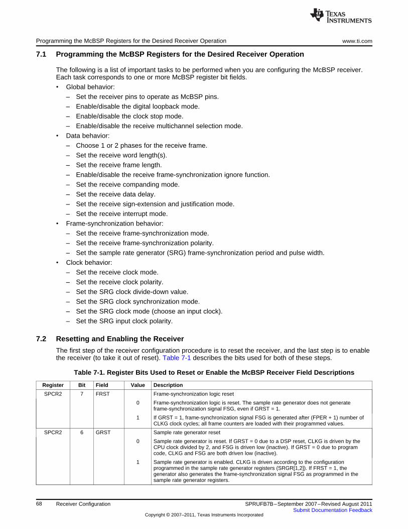
Programming the McBSP Registers for the Desired Receiver Operation www.ti.com
7.1 Programming the McBSP Registers for the Desired Receiver Operation
The following is a list of important tasks to be performed when you are configuring the McBSP receiver.Each task corresponds to one or more McBSP register bit fields.
• Global behavior:
– Set the receiver pins to operate as McBSP pins.
– Enable/disable the digital loopback mode.
– Enable/disable the clock stop mode.
– Enable/disable the receive multichannel selection mode.
• Data behavior:
– Choose 1 or 2 phases for the receive frame.
– Set the receive word length(s).
– Set the receive frame length.
– Enable/disable the receive frame-synchronization ignore function.
– Set the receive companding mode.
– Set the receive data delay.
– Set the receive sign-extension and justification mode.
– Set the receive interrupt mode.
• Frame-synchronization behavior:
– Set the receive frame-synchronization mode.
– Set the receive frame-synchronization polarity.
– Set the sample rate generator (SRG) frame-synchronization period and pulse width.
• Clock behavior:
– Set the receive clock mode.
– Set the receive clock polarity.
– Set the SRG clock divide-down value.
– Set the SRG clock synchronization mode.
– Set the SRG clock mode (choose an input clock).
– Set the SRG input clock polarity.
7.2 Resetting and Enabling the Receiver
The first step of the receiver configuration procedure is to reset the receiver, and the last step is to enablethe receiver (to take it out of reset). Table 7-1 describes the bits used for both of these steps.
Table 7-1. Register Bits Used to Reset or Enable the McBSP Receiver Field Descriptions
Register Bit Field Value Description
SPCR2 7 FRST Frame-synchronization logic reset
0 Frame-synchronization logic is reset. The sample rate generator does not generateframe-synchronization signal FSG, even if GRST = 1.
1 If GRST = 1, frame-synchronization signal FSG is generated after (FPER + 1) number ofCLKG clock cycles; all frame counters are loaded with their programmed values.
SPCR2 6 GRST Sample rate generator reset
0 Sample rate generator is reset. If GRST = 0 due to a DSP reset, CLKG is driven by theCPU clock divided by 2, and FSG is driven low (inactive). If GRST = 0 due to programcode, CLKG and FSG are both driven low (inactive).
1 Sample rate generator is enabled. CLKG is driven according to the configurationprogrammed in the sample rate generator registers (SRGR[1,2]). If FRST = 1, thegenerator also generates the frame-synchronization signal FSG as programmed in thesample rate generator registers.
68 Receiver Configuration SPRUFB7B–September 2007–Revised August 2011Submit Documentation Feedback
Copyright © 2007–2011, Texas Instruments Incorporated
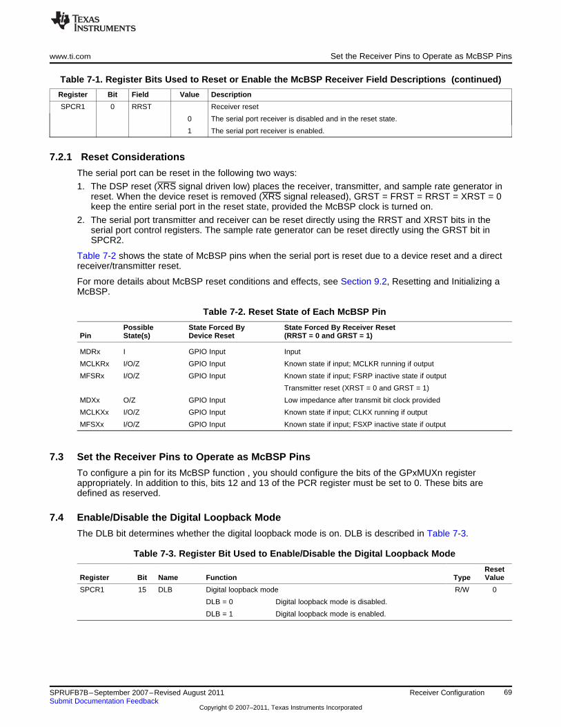
www.ti.com Set the Receiver Pins to Operate as McBSP Pins
Table 7-1. Register Bits Used to Reset or Enable the McBSP Receiver Field Descriptions (continued)
Register Bit Field Value Description
SPCR1 0 RRST Receiver reset
0 The serial port receiver is disabled and in the reset state.
1 The serial port receiver is enabled.
7.2.1 Reset Considerations
The serial port can be reset in the following two ways:
1. The DSP reset (XRS signal driven low) places the receiver, transmitter, and sample rate generator inreset. When the device reset is removed (XRS signal released), GRST = FRST = RRST = XRST = 0keep the entire serial port in the reset state, provided the McBSP clock is turned on.
2. The serial port transmitter and receiver can be reset directly using the RRST and XRST bits in theserial port control registers. The sample rate generator can be reset directly using the GRST bit inSPCR2.
Table 7-2 shows the state of McBSP pins when the serial port is reset due to a device reset and a directreceiver/transmitter reset.
For more details about McBSP reset conditions and effects, see Section 9.2, Resetting and Initializing aMcBSP.
Table 7-2. Reset State of Each McBSP Pin
Possible State Forced By State Forced By Receiver ResetPin State(s) Device Reset (RRST = 0 and GRST = 1)
MDRx I GPIO Input Input
MCLKRx I/O/Z GPIO Input Known state if input; MCLKR running if output
MFSRx I/O/Z GPIO Input Known state if input; FSRP inactive state if output
Transmitter reset (XRST = 0 and GRST = 1)
MDXx O/Z GPIO Input Low impedance after transmit bit clock provided
MCLKXx I/O/Z GPIO Input Known state if input; CLKX running if output
MFSXx I/O/Z GPIO Input Known state if input; FSXP inactive state if output
7.3 Set the Receiver Pins to Operate as McBSP Pins
To configure a pin for its McBSP function , you should configure the bits of the GPxMUXn registerappropriately. In addition to this, bits 12 and 13 of the PCR register must be set to 0. These bits aredefined as reserved.
7.4 Enable/Disable the Digital Loopback Mode
The DLB bit determines whether the digital loopback mode is on. DLB is described in Table 7-3.
Table 7-3. Register Bit Used to Enable/Disable the Digital Loopback Mode
ResetRegister Bit Name Function Type Value
SPCR1 15 DLB Digital loopback mode R/W 0
DLB = 0 Digital loopback mode is disabled.
DLB = 1 Digital loopback mode is enabled.
69SPRUFB7B–September 2007–Revised August 2011 Receiver ConfigurationSubmit Documentation Feedback
Copyright © 2007–2011, Texas Instruments Incorporated
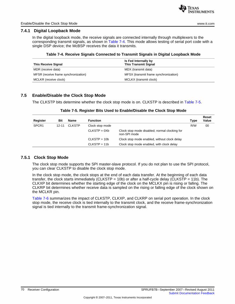
Enable/Disable the Clock Stop Mode www.ti.com
7.4.1 Digital Loopback Mode
In the digital loopback mode, the receive signals are connected internally through multiplexers to thecorresponding transmit signals, as shown in Table 7-4. This mode allows testing of serial port code with asingle DSP device; the McBSP receives the data it transmits.
Table 7-4. Receive Signals Connected to Transmit Signals in Digital Loopback Mode
Is Fed Internally byThis Receive Signal This Transmit Signal
MDR (receive data) MDX (transmit data)
MFSR (receive frame synchronization) MFSX (transmit frame synchronization)
MCLKR (receive clock) MCLKX (transmit clock)
7.5 Enable/Disable the Clock Stop Mode
The CLKSTP bits determine whether the clock stop mode is on. CLKSTP is described in Table 7-5.
Table 7-5. Register Bits Used to Enable/Disable the Clock Stop Mode
ResetRegister Bit Name Function Type Value
SPCR1 12-11 CLKSTP Clock stop mode R/W 00
CLKSTP = 0Xb Clock stop mode disabled; normal clocking fornon-SPI mode
CLKSTP = 10b Clock stop mode enabled, without clock delay
CLKSTP = 11b Clock stop mode enabled, with clock delay
7.5.1 Clock Stop Mode
The clock stop mode supports the SPI master-slave protocol. If you do not plan to use the SPI protocol,you can clear CLKSTP to disable the clock stop mode.
In the clock stop mode, the clock stops at the end of each data transfer. At the beginning of each datatransfer, the clock starts immediately (CLKSTP = 10b) or after a half-cycle delay (CLKSTP = 11b). TheCLKXP bit determines whether the starting edge of the clock on the MCLKX pin is rising or falling. TheCLKRP bit determines whether receive data is sampled on the rising or falling edge of the clock shown onthe MCLKR pin.
Table 7-6 summarizes the impact of CLKSTP, CLKXP, and CLKRP on serial port operation. In the clockstop mode, the receive clock is tied internally to the transmit clock, and the receive frame-synchronizationsignal is tied internally to the transmit frame-synchronization signal.
70 Receiver Configuration SPRUFB7B–September 2007–Revised August 2011Submit Documentation Feedback
Copyright © 2007–2011, Texas Instruments Incorporated
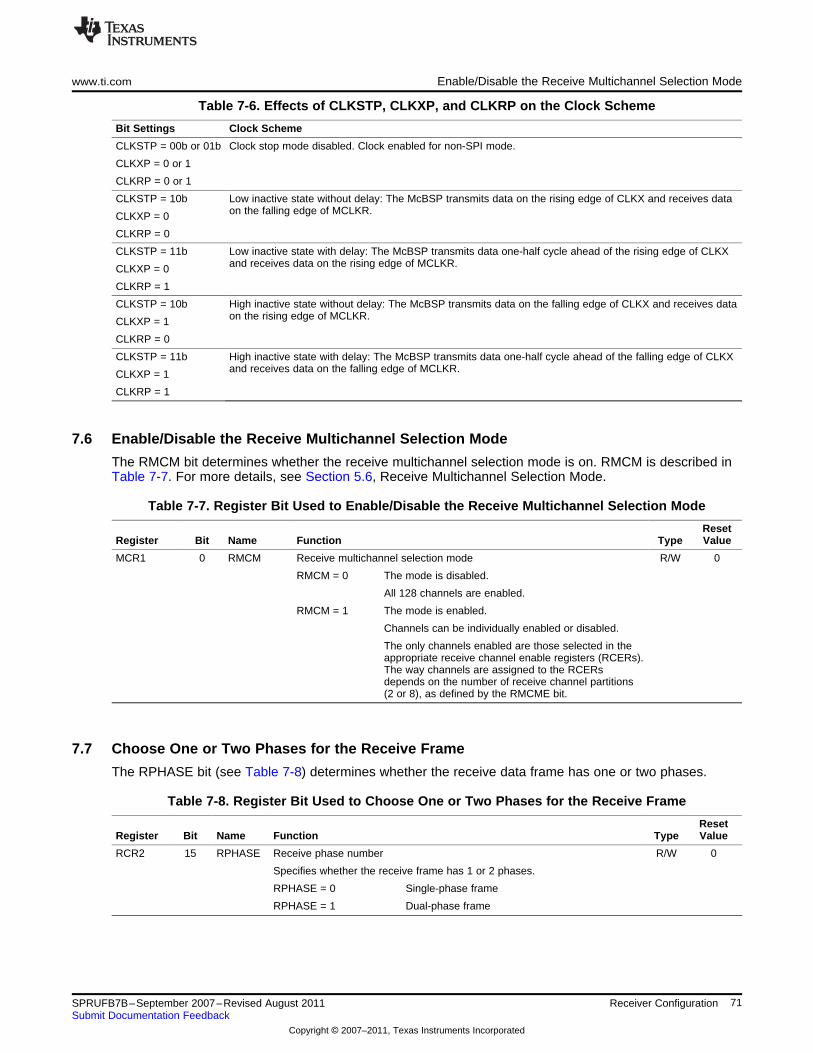
www.ti.com Enable/Disable the Receive Multichannel Selection Mode
Table 7-6. Effects of CLKSTP, CLKXP, and CLKRP on the Clock Scheme
Bit Settings Clock Scheme
CLKSTP = 00b or 01b Clock stop mode disabled. Clock enabled for non-SPI mode.
CLKXP = 0 or 1
CLKRP = 0 or 1
CLKSTP = 10b Low inactive state without delay: The McBSP transmits data on the rising edge of CLKX and receives dataon the falling edge of MCLKR.CLKXP = 0
CLKRP = 0
CLKSTP = 11b Low inactive state with delay: The McBSP transmits data one-half cycle ahead of the rising edge of CLKXand receives data on the rising edge of MCLKR.CLKXP = 0
CLKRP = 1
CLKSTP = 10b High inactive state without delay: The McBSP transmits data on the falling edge of CLKX and receives dataon the rising edge of MCLKR.CLKXP = 1
CLKRP = 0
CLKSTP = 11b High inactive state with delay: The McBSP transmits data one-half cycle ahead of the falling edge of CLKXand receives data on the falling edge of MCLKR.CLKXP = 1
CLKRP = 1
7.6 Enable/Disable the Receive Multichannel Selection Mode
The RMCM bit determines whether the receive multichannel selection mode is on. RMCM is described inTable 7-7. For more details, see Section 5.6, Receive Multichannel Selection Mode.
Table 7-7. Register Bit Used to Enable/Disable the Receive Multichannel Selection Mode
ResetRegister Bit Name Function Type Value
MCR1 0 RMCM Receive multichannel selection mode R/W 0
RMCM = 0 The mode is disabled.
All 128 channels are enabled.
RMCM = 1 The mode is enabled.
Channels can be individually enabled or disabled.
The only channels enabled are those selected in theappropriate receive channel enable registers (RCERs).The way channels are assigned to the RCERsdepends on the number of receive channel partitions(2 or 8), as defined by the RMCME bit.
7.7 Choose One or Two Phases for the Receive Frame
The RPHASE bit (see Table 7-8) determines whether the receive data frame has one or two phases.
Table 7-8. Register Bit Used to Choose One or Two Phases for the Receive Frame
ResetRegister Bit Name Function Type Value
RCR2 15 RPHASE Receive phase number R/W 0
Specifies whether the receive frame has 1 or 2 phases.
RPHASE = 0 Single-phase frame
RPHASE = 1 Dual-phase frame
71SPRUFB7B–September 2007–Revised August 2011 Receiver ConfigurationSubmit Documentation Feedback
Copyright © 2007–2011, Texas Instruments Incorporated
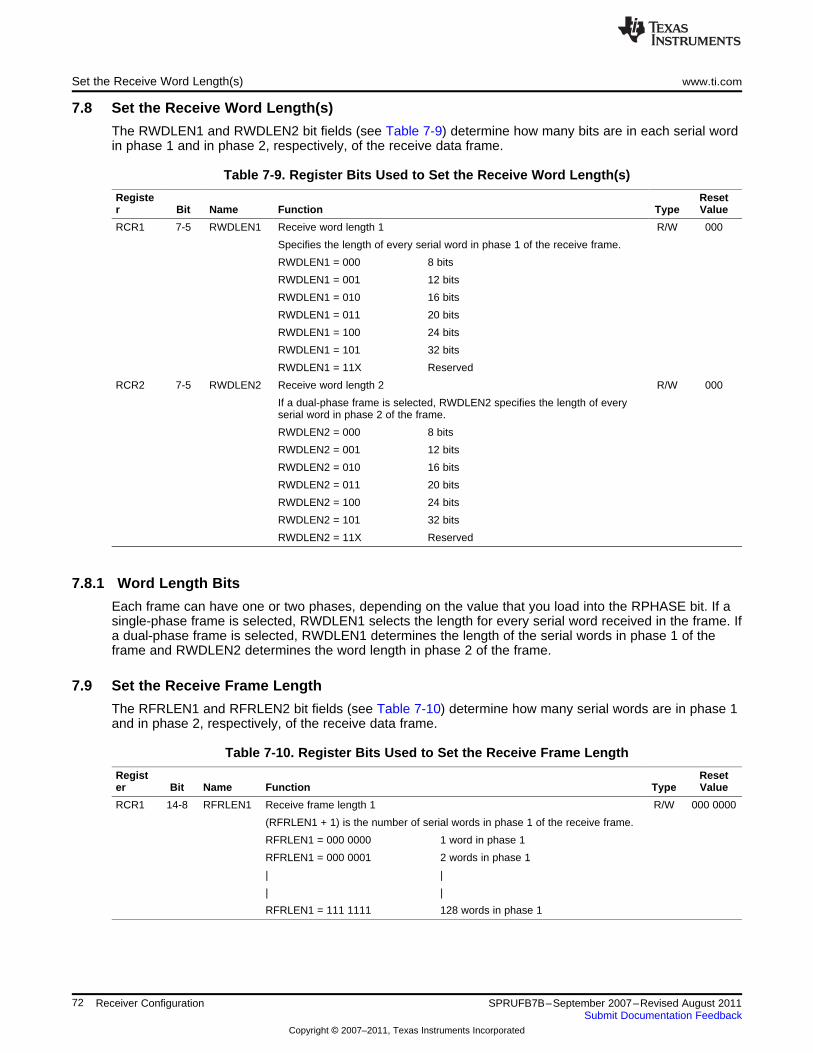
Set the Receive Word Length(s) www.ti.com
7.8 Set the Receive Word Length(s)
The RWDLEN1 and RWDLEN2 bit fields (see Table 7-9) determine how many bits are in each serial wordin phase 1 and in phase 2, respectively, of the receive data frame.
Table 7-9. Register Bits Used to Set the Receive Word Length(s)
Registe Resetr Bit Name Function Type Value
RCR1 7-5 RWDLEN1 Receive word length 1 R/W 000
Specifies the length of every serial word in phase 1 of the receive frame.
RWDLEN1 = 000 8 bits
RWDLEN1 = 001 12 bits
RWDLEN1 = 010 16 bits
RWDLEN1 = 011 20 bits
RWDLEN1 = 100 24 bits
RWDLEN1 = 101 32 bits
RWDLEN1 = 11X Reserved
RCR2 7-5 RWDLEN2 Receive word length 2 R/W 000
If a dual-phase frame is selected, RWDLEN2 specifies the length of everyserial word in phase 2 of the frame.
RWDLEN2 = 000 8 bits
RWDLEN2 = 001 12 bits
RWDLEN2 = 010 16 bits
RWDLEN2 = 011 20 bits
RWDLEN2 = 100 24 bits
RWDLEN2 = 101 32 bits
RWDLEN2 = 11X Reserved
7.8.1 Word Length Bits
Each frame can have one or two phases, depending on the value that you load into the RPHASE bit. If asingle-phase frame is selected, RWDLEN1 selects the length for every serial word received in the frame. Ifa dual-phase frame is selected, RWDLEN1 determines the length of the serial words in phase 1 of theframe and RWDLEN2 determines the word length in phase 2 of the frame.
7.9 Set the Receive Frame Length
The RFRLEN1 and RFRLEN2 bit fields (see Table 7-10) determine how many serial words are in phase 1and in phase 2, respectively, of the receive data frame.
Table 7-10. Register Bits Used to Set the Receive Frame Length
Regist Reseter Bit Name Function Type Value
RCR1 14-8 RFRLEN1 Receive frame length 1 R/W 000 0000
(RFRLEN1 + 1) is the number of serial words in phase 1 of the receive frame.
RFRLEN1 = 000 0000 1 word in phase 1
RFRLEN1 = 000 0001 2 words in phase 1
| |
| |
RFRLEN1 = 111 1111 128 words in phase 1
72 Receiver Configuration SPRUFB7B–September 2007–Revised August 2011Submit Documentation Feedback
Copyright © 2007–2011, Texas Instruments Incorporated
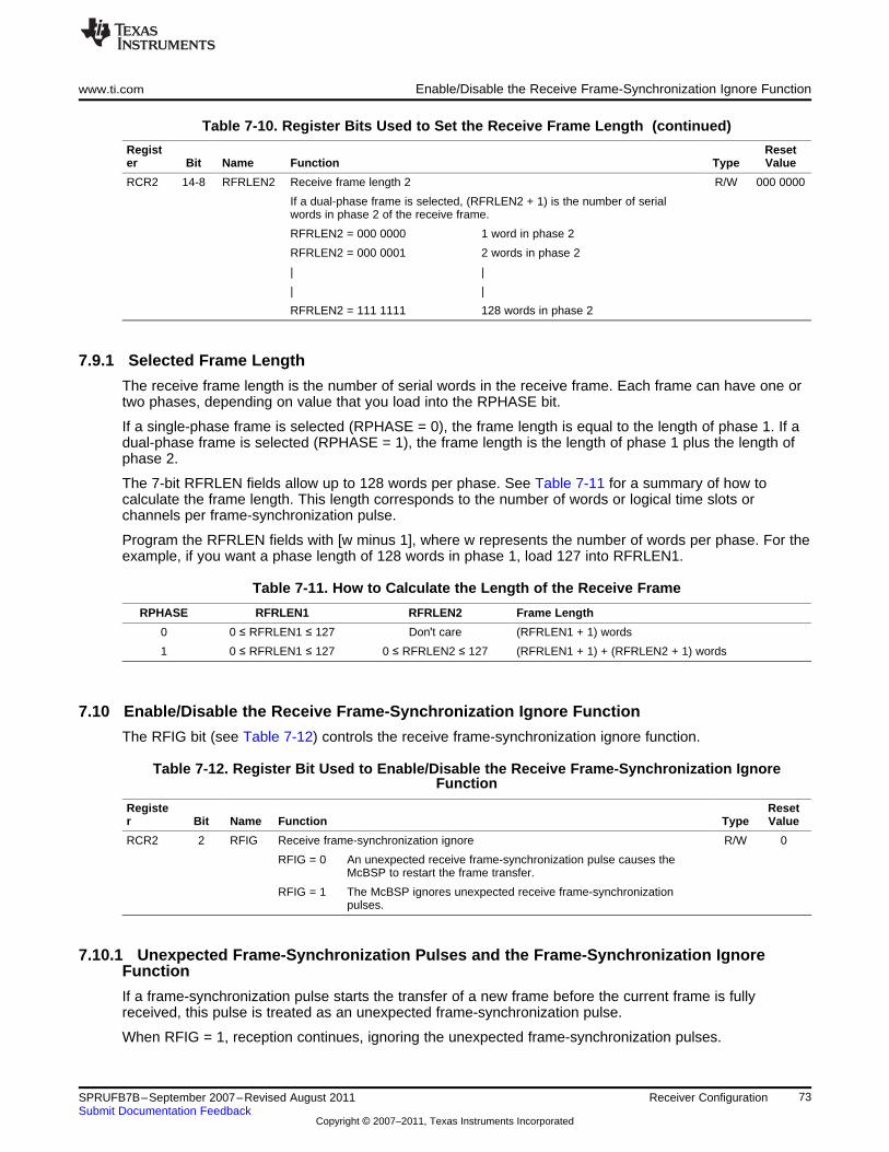
www.ti.com Enable/Disable the Receive Frame-Synchronization Ignore Function
Table 7-10. Register Bits Used to Set the Receive Frame Length (continued)
Regist Reseter Bit Name Function Type Value
RCR2 14-8 RFRLEN2 Receive frame length 2 R/W 000 0000
If a dual-phase frame is selected, (RFRLEN2 + 1) is the number of serialwords in phase 2 of the receive frame.
RFRLEN2 = 000 0000 1 word in phase 2
RFRLEN2 = 000 0001 2 words in phase 2
| |
| |
RFRLEN2 = 111 1111 128 words in phase 2
7.9.1 Selected Frame Length
The receive frame length is the number of serial words in the receive frame. Each frame can have one ortwo phases, depending on value that you load into the RPHASE bit.
If a single-phase frame is selected (RPHASE = 0), the frame length is equal to the length of phase 1. If adual-phase frame is selected (RPHASE = 1), the frame length is the length of phase 1 plus the length ofphase 2.
The 7-bit RFRLEN fields allow up to 128 words per phase. See Table 7-11 for a summary of how tocalculate the frame length. This length corresponds to the number of words or logical time slots orchannels per frame-synchronization pulse.
Program the RFRLEN fields with [w minus 1], where w represents the number of words per phase. For theexample, if you want a phase length of 128 words in phase 1, load 127 into RFRLEN1.
Table 7-11. How to Calculate the Length of the Receive Frame
RPHASE RFRLEN1 RFRLEN2 Frame Length
0 0 ≤ RFRLEN1 ≤ 127 Don't care (RFRLEN1 + 1) words
1 0 ≤ RFRLEN1 ≤ 127 0 ≤ RFRLEN2 ≤ 127 (RFRLEN1 + 1) + (RFRLEN2 + 1) words
7.10 Enable/Disable the Receive Frame-Synchronization Ignore Function
The RFIG bit (see Table 7-12) controls the receive frame-synchronization ignore function.
Table 7-12. Register Bit Used to Enable/Disable the Receive Frame-Synchronization IgnoreFunction
Registe Resetr Bit Name Function Type Value
RCR2 2 RFIG Receive frame-synchronization ignore R/W 0
RFIG = 0 An unexpected receive frame-synchronization pulse causes theMcBSP to restart the frame transfer.
RFIG = 1 The McBSP ignores unexpected receive frame-synchronizationpulses.
7.10.1 Unexpected Frame-Synchronization Pulses and the Frame-Synchronization IgnoreFunction
If a frame-synchronization pulse starts the transfer of a new frame before the current frame is fullyreceived, this pulse is treated as an unexpected frame-synchronization pulse.
When RFIG = 1, reception continues, ignoring the unexpected frame-synchronization pulses.
73SPRUFB7B–September 2007–Revised August 2011 Receiver ConfigurationSubmit Documentation Feedback
Copyright © 2007–2011, Texas Instruments Incorporated
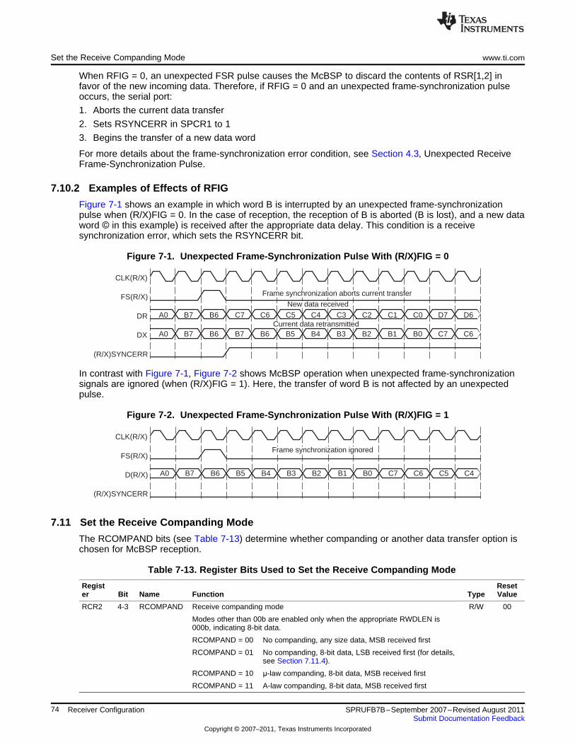
Current data retransmitted
New data received
(R/X)SYNCERR
DX
DR
FS(R/X)
CLK(R/X)
C6C7B0
ÁÁÁÁÁÁB2B3B4B5B7 B6B6B7A0 B1
D6D7C0C1C2C3C4C5C6C7B6B7A0
ÁÁÁÁÁÁÁÁFrame synchronization aborts current transfer
(R/X)SYNCERR
D(R/X)
FS(R/X)
CLK(R/X)
C4C5C6C7B0B1B2B3B4B5B6B7A0
ÁÁÁÁÁÁÁÁFrame synchronization ignored
Set the Receive Companding Mode www.ti.com
When RFIG = 0, an unexpected FSR pulse causes the McBSP to discard the contents of RSR[1,2] infavor of the new incoming data. Therefore, if RFIG = 0 and an unexpected frame-synchronization pulseoccurs, the serial port:
1. Aborts the current data transfer
2. Sets RSYNCERR in SPCR1 to 1
3. Begins the transfer of a new data word
For more details about the frame-synchronization error condition, see Section 4.3, Unexpected ReceiveFrame-Synchronization Pulse.
7.10.2 Examples of Effects of RFIG
Figure 7-1 shows an example in which word B is interrupted by an unexpected frame-synchronizationpulse when (R/X)FIG = 0. In the case of reception, the reception of B is aborted (B is lost), and a new dataword © in this example) is received after the appropriate data delay. This condition is a receivesynchronization error, which sets the RSYNCERR bit.
Figure 7-1. Unexpected Frame-Synchronization Pulse With (R/X)FIG = 0
In contrast with Figure 7-1, Figure 7-2 shows McBSP operation when unexpected frame-synchronizationsignals are ignored (when (R/X)FIG = 1). Here, the transfer of word B is not affected by an unexpectedpulse.
Figure 7-2. Unexpected Frame-Synchronization Pulse With (R/X)FIG = 1
7.11 Set the Receive Companding Mode
The RCOMPAND bits (see Table 7-13) determine whether companding or another data transfer option ischosen for McBSP reception.
Table 7-13. Register Bits Used to Set the Receive Companding Mode
Regist Reseter Bit Name Function Type Value
RCR2 4-3 RCOMPAND Receive companding mode R/W 00
Modes other than 00b are enabled only when the appropriate RWDLEN is000b, indicating 8-bit data.
RCOMPAND = 00 No companding, any size data, MSB received first
RCOMPAND = 01 No companding, 8-bit data, LSB received first (for details,see Section 7.11.4).
RCOMPAND = 10 μ-law companding, 8-bit data, MSB received first
RCOMPAND = 11 A-law companding, 8-bit data, MSB received first
74 Receiver Configuration SPRUFB7B–September 2007–Revised August 2011Submit Documentation Feedback
Copyright © 2007–2011, Texas Instruments Incorporated
From CPU or DMA controllerDXR1
To CPU or DMA controllerDRR1
16
16
DX8
8
XSR1 Compress
ExpandDR RBR1RSR1
www.ti.com Set the Receive Data Delay
7.11.1 Companding
Companding (COMpressing and exPANDing) hardware allows compression and expansion of data ineither μ-law or A-law format. The companding standard employed in the United States and Japan is μ-law.The European companding standard is referred to as A-law. The specifications for μ-law and A-law logPCM are part of the CCITT G.711 recommendation.
A-law and μ-law allow 13 bits and 14 bits of dynamic range, respectively. Any values outside this rangeare set to the most positive or most negative value. Thus, for companding to work best, the datatransferred to and from the McBSP via the CPU or DMA controller must be at least 16 bits wide.
The μ-law and A-law formats both encode data into 8-bit code words. Companded data is always 8 bitswide; the appropriate word length bits (RWDLEN1, RWDLEN2, XWDLEN1, XWDLEN2) must therefore beset to 0, indicating an 8-bit wide serial data stream. If companding is enabled and either of the framephases does not have an 8-bit word length, companding continues as if the word length is 8 bits.
Figure 7-3 illustrates the companding processes. When companding is chosen for the transmitter,compression occurs during the process of copying data from DXR1 to XSR1. The transmit data isencoded according to the specified companding law (A-law or μ-law). When companding is chosen for thereceiver, expansion occurs during the process of copying data from RBR1 to DRR1. The receive data isdecoded to 2's-complement format.
Figure 7-3. Companding Processes for Reception and for Transmission
7.11.2 Format of Expanded Data
For reception, the 8-bit compressed data in RBR1 is expanded to left-justified 16-bit data in DRR1. TheRJUST bit of SPCR1 is ignored when companding is used.
7.11.3 Companding Internal Data
If the McBSP is otherwise unused (the serial port transmit and receive sections are reset), thecompanding hardware can compand internal data. See Section 2.2.2, Capability to Compand InternalData.
7.11.4 Option to Receive LSB First
Normally, the McBSP transmits or receives all data with the most significant bit (MSB) first. However,certain 8-bit data protocols (that do not use companded data) require the least significant bit (LSB) to betransferred first. If you set RCOMPAND = 01b in RCR2, the bit ordering of 8-bit words is reversed duringreception. Similar to companding, this feature is enabled only if the appropriate word length bits are set to0, indicating that 8-bit words are to be transferred serially. If either phase of the frame does not have an8-bit word length, the McBSP assumes the word length is eight bits and LSB-first ordering is done.
7.12 Set the Receive Data Delay
The RDATDLY bits (see Table 7-14) determine the length of the data delay for the receive frame.
Table 7-14. Register Bits Used to Set the Receive Data Delay
ResetRegister Bit Name Function Type Value
RCR2 1-0 RDATDLY Receive data delay R/W 00
RDATDLY = 00 0-bit data delay
RDATDLY = 01 1-bit data delay
RDATDLY = 10 2-bit data delay
75SPRUFB7B–September 2007–Revised August 2011 Receiver ConfigurationSubmit Documentation Feedback
Copyright © 2007–2011, Texas Instruments Incorporated
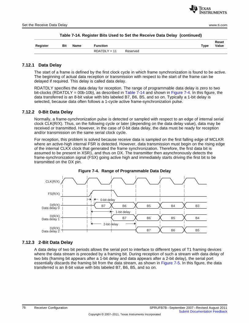
B5B6B7
B4B5B6B7
B3B4B5B6B7
Data delay 2D(R/X)
Data delay 1D(R/X)
Data delay 0D(R/X)
FS(R/X)
CLK(R/X)
1-bit delayÁÁÁÁÁÁÁÁÁÁÁÁÁÁÁÁ0-bit delay
2-bit delay
Set the Receive Data Delay www.ti.com
Table 7-14. Register Bits Used to Set the Receive Data Delay (continued)
ResetRegister Bit Name Function Type Value
RDATDLY = 11 Reserved
7.12.1 Data Delay
The start of a frame is defined by the first clock cycle in which frame synchronization is found to be active.The beginning of actual data reception or transmission with respect to the start of the frame can bedelayed if required. This delay is called data delay.
RDATDLY specifies the data delay for reception. The range of programmable data delay is zero to twobit-clocks (RDATDLY = 00b-10b), as described in Table 7-14 and shown in Figure 7-4. In this figure, thedata transferred is an 8-bit value with bits labeled B7, B6, B5, and so on. Typically a 1-bit delay isselected, because data often follows a 1-cycle active frame-synchronization pulse.
7.12.2 0-Bit Data Delay
Normally, a frame-synchronization pulse is detected or sampled with respect to an edge of internal serialclock CLK(R/X). Thus, on the following cycle or later (depending on the data delay value), data may bereceived or transmitted. However, in the case of 0-bit data delay, the data must be ready for receptionand/or transmission on the same serial clock cycle.
For reception, this problem is solved because receive data is sampled on the first falling edge of MCLKRwhere an active-high internal FSR is detected. However, data transmission must begin on the rising edgeof the internal CLKX clock that generated the frame synchronization. Therefore, the first data bit isassumed to be present in XSR1, and thus on DX. The transmitter then asynchronously detects theframe-synchronization signal (FSX) going active high and immediately starts driving the first bit to betransmitted on the DX pin.
Figure 7-4. Range of Programmable Data Delay
7.12.3 2-Bit Data Delay
A data delay of two bit periods allows the serial port to interface to different types of T1 framing deviceswhere the data stream is preceded by a framing bit. During reception of such a stream with data delay oftwo bits (framing bit appears after a 1-bit delay and data appears after a 2-bit delay), the serial portessentially discards the framing bit from the data stream, as shown in Figure 7-5. In this figure, the datatransferred is an 8-bit value with bits labeled B7, B6, B5, and so on.
76 Receiver Configuration SPRUFB7B–September 2007–Revised August 2011Submit Documentation Feedback
Copyright © 2007–2011, Texas Instruments Incorporated
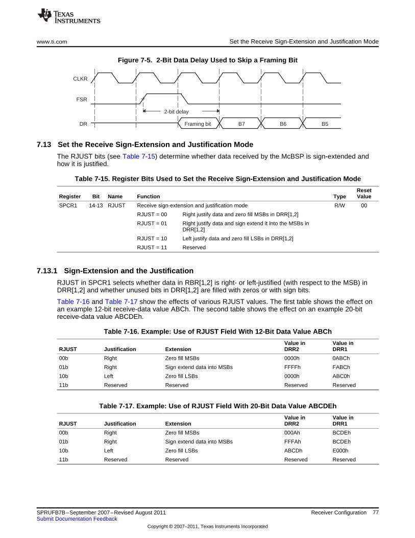
DR Framing bit B5B6B7
FSR
CLKR ÁÁÁÁ2-bit delay
www.ti.com Set the Receive Sign-Extension and Justification Mode
Figure 7-5. 2-Bit Data Delay Used to Skip a Framing Bit
7.13 Set the Receive Sign-Extension and Justification Mode
The RJUST bits (see Table 7-15) determine whether data received by the McBSP is sign-extended andhow it is justified.
Table 7-15. Register Bits Used to Set the Receive Sign-Extension and Justification Mode
ResetRegister Bit Name Function Type Value
SPCR1 14-13 RJUST Receive sign-extension and justification mode R/W 00
RJUST = 00 Right justify data and zero fill MSBs in DRR[1,2]
RJUST = 01 Right justify data and sign extend it into the MSBs inDRR[1,2]
RJUST = 10 Left justify data and zero fill LSBs in DRR[1,2]
RJUST = 11 Reserved
7.13.1 Sign-Extension and the Justification
RJUST in SPCR1 selects whether data in RBR[1,2] is right- or left-justified (with respect to the MSB) inDRR[1,2] and whether unused bits in DRR[1,2] are filled with zeros or with sign bits.
Table 7-16 and Table 7-17 show the effects of various RJUST values. The first table shows the effect onan example 12-bit receive-data value ABCh. The second table shows the effect on an example 20-bitreceive-data value ABCDEh.
Table 7-16. Example: Use of RJUST Field With 12-Bit Data Value ABCh
Value in Value inRJUST Justification Extension DRR2 DRR1
00b Right Zero fill MSBs 0000h 0ABCh
01b Right Sign extend data into MSBs FFFFh FABCh
10b Left Zero fill LSBs 0000h ABC0h
11b Reserved Reserved Reserved Reserved
Table 7-17. Example: Use of RJUST Field With 20-Bit Data Value ABCDEh
Value in Value inRJUST Justification Extension DRR2 DRR1
00b Right Zero fill MSBs 000Ah BCDEh
01b Right Sign extend data into MSBs FFFAh BCDEh
10b Left Zero fill LSBs ABCDh E000h
11b Reserved Reserved Reserved Reserved
77SPRUFB7B–September 2007–Revised August 2011 Receiver ConfigurationSubmit Documentation Feedback
Copyright © 2007–2011, Texas Instruments Incorporated
Set the Receive Sign-Extension and Justification Mode www.ti.com
78 Receiver Configuration SPRUFB7B–September 2007–Revised August 2011Submit Documentation Feedback
Copyright © 2007–2011, Texas Instruments Incorporated
www.ti.com Set the Receive Interrupt Mode
7.14 Set the Receive Interrupt Mode
The RINTM bits (see Table 7-18) determine which event generates a receive interrupt request to the CPU.
The receive interrupt (RINT) informs the CPU of changes to the serial port status. Four options exist forconfiguring this interrupt. The options are set by the receive interrupt mode bits, RINTM, in SPCR1.
Table 7-18. Register Bits Used to Set the Receive Interrupt Mode
ResetRegister Bit Name Function Type Value
SPCR1 5-4 RINTM Receive interrupt mode R/W 00
RINTM = 00 RINT generated when RRDY changes from 0 to 1. Interrupt onevery serial word by tracking the RRDY bit in SPCR1.Regardless of the value of RINTM, RRDY can be read todetect the RRDY = 1 condition.
RINTM = 01 RINT generated by an end-of-block or end-of-frame conditionin the receive multichannel selection mode. In the multichannelselection mode, interrupt after every 16-channel blockboundary has been crossed within a frame and at the end ofthe frame. For details, see Section 5.8, Using InterruptsBetween Block Transfers. In any other serial transfer case, thissetting is not applicable and, therefore, no interrupts aregenerated.
RINTM = 10 RINT generated by a new receive frame-synchronization pulse.Interrupt on detection of receive frame-synchronization pulses.This generates an interrupt even when the receiver is in itsreset state. This is done by synchronizing the incomingframe-synchronization pulse to the CPU clock and sending it tothe CPU via RINT.
RINTM = 11 RINT generated when RSYNCERR is set. Interrupt onframe-synchronization error. Regardless of the value of RINTM,RSYNCERR can be read to detect this condition. Forinformation on using RSYNCERR, see Section 4.3,Unexpected Receive Frame-Synchronization Pulse.
7.15 Set the Receive Frame-Synchronization Mode
The bits described in Table 7-19 determine the source for receive frame synchronization and the functionof the FSR pin.
7.15.1 Receive Frame-Synchronization Modes
Table 7-20 shows how you can select various sources to provide the receive frame-synchronization signaland the effect on the FSR pin. The polarity of the signal on the FSR pin is determined by the FSRP bit.
In digital loopback mode (DLB = 1), the transmit frame-synchronization signal is used as the receiveframe-synchronization signal.
Also in the clock stop mode, the internal receive clock signal (MCLKR) and the internal receiveframe-synchronization signal (FSR) are internally connected to their transmit counterparts, CLKX andFSX.
Table 7-19. Register Bits Used to Set the Receive Frame Synchronization Mode
ResetRegister Bit Name Function Type Value
PCR 10 FSRM Receive frame-synchronization mode R/W 0
FSRM = 0 Receive frame synchronization is supplied by anexternal source via the FSR pin.
FSRM = 1 Receive frame synchronization is supplied bythe sample rate generator. FSR is an output pinreflecting internal FSR, except when GSYNC = 1in SRGR2.
79SPRUFB7B–September 2007–Revised August 2011 Receiver ConfigurationSubmit Documentation Feedback
Copyright © 2007–2011, Texas Instruments Incorporated
Set the Receive Frame-Synchronization Mode www.ti.com
Table 7-19. Register Bits Used to Set the Receive Frame Synchronization Mode (continued)
ResetRegister Bit Name Function Type Value
SRGR2 15 GSYNC Sample rate generator clock synchronization mode R/W 0
If the sample rate generator creates a frame-synchronization signal(FSG) that is derived from an external input clock, the GSYNC bitdetermines whether FSG is kept synchronized with pulses on the FSRpin.
GSYNC = 0 No clock synchronization is used: CLKGoscillates without adjustment, and FSG pulsesevery (FPER + 1) CLKG cycles.
GSYNC = 1 Clock synchronization is used. When a pulse isdetected on the FSR pin:• CLKG is adjusted as necessary so that it is
synchronized with the input clock on theMCLKR pin.
• FSG pulses FSG only pulses in responseto a pulse on the FSR pin. Theframe-synchronization period defined inFPER is ignored.
For more details, see Section 3.3, SynchronizingSample Rate Generator Outputs to an ExternalClock.
SPCR1 15 DLB Digital loopback mode R/W 0
DLB = 0 Digital loopback mode is disabled.
DLB = 1 Digital loopback mode is enabled. The receivesignals, including the receiveframe-synchronization signal, are connectedinternally through multiplexers to thecorresponding transmit signals.
SPCR1 12-11 CLKSTP Clock stop mode R/W 00
CLKSTP = 0Xb Clock stop mode disabled; normal clocking fornon-SPI mode.
CLKSTP = 10b Clock stop mode enabled without clock delay.The internal receive clock signal (MCLKR) andthe internal receive frame-synchronization signal(FSR) are internally connected to their transmitcounterparts, CLKX and FSX.
CLKSTP = 11b Clock stop mode enabled with clock delay. Theinternal receive clock signal (MCLKR) and theinternal receive frame-synchronization signal(FSR) are internally connected to their transmitcounterparts, CLKX and FSX.
Table 7-20. Select Sources to Provide the Receive Frame-Synchronization Signal and the Effect onthe FSR Pin
Source of Receive FrameDLB FSRM GSYNC Synchronization FSR Pin Status
0 0 0 or 1 An external frame-synchronization signal Inputenters the McBSP through the FSR pin.The signal is then inverted as determinedby FSRP before being used as internalFSR.
0 1 0 Internal FSR is driven by the sample rate Output. FSG is inverted as determined bygenerator frame-synchronization signal FSRP before being driven out on the(FSG). FSR pin.
0 1 1 Internal FSR is driven by the sample rate Input. The external frame-synchronizationgenerator frame-synchronization signal input on the FSR pin is used to(FSG). synchronize CLKG and generate FSG
pulses.
1 0 0 Internal FSX drives internal FSR. High impedance
80 Receiver Configuration SPRUFB7B–September 2007–Revised August 2011Submit Documentation Feedback
Copyright © 2007–2011, Texas Instruments Incorporated
www.ti.com Set the Receive Frame-Synchronization Polarity
Table 7-20. Select Sources to Provide the Receive Frame-Synchronization Signal and the Effect onthe FSR Pin (continued)
Source of Receive FrameDLB FSRM GSYNC Synchronization FSR Pin Status
1 0 or 1 1 Internal FSX drives internal FSR. Input. If the sample rate generator isrunning, external FSR is used tosynchronize CLKG and generate FSGpulses.
1 1 0 Internal FSX drives internal FSR. Output. Receive (same as transmit)frame synchronization is inverted asdetermined by FSRP before being drivenout on the FSR pin.
7.16 Set the Receive Frame-Synchronization Polarity
The FSRP bit (see Table 7-21) determines whether frame-synchronization pulses are active high or activelow on the FSR pin.
Table 7-21. Register Bit Used to Set Receive Frame-Synchronization Polarity
ResetRegister Bit Name Function Type Value
PCR 2 FSRP Receive frame-synchronization polarity R/W 0
FSRP = 0 Frame-synchronization pulse FSR is active high.
FSRP = 1 Frame-synchronization pulse FSR is active low.
7.16.1 Frame-Synchronization Pulses, Clock Signals, and Their Polarities
Receive frame-synchronization pulses can be generated internally by the sample rate generator (seeSection 3.2) or driven by an external source. The source of frame synchronization is selected byprogramming the mode bit, FSRM, in PCR. FSR is also affected by the GSYNC bit in SRGR2. Forinformation about the effects of FSRM and GSYNC, see Section 7.15, Set the ReceiveFrame-Synchronization Mode. Similarly, receive clocks can be selected to be inputs or outputs byprogramming the mode bit, CLKRM, in the PCR (see Section 7.17, Set the Receive Clock Mode).
When FSR and FSX are inputs (FSXM = FSRM= 0, external frame-synchronization pulses), the McBSPdetects them on the internal falling edge of clock, internal MCLKR, and internal CLKX, respectively. Thereceive data arriving at the DR pin is also sampled on the falling edge of internal MCLKR. These internalclock signals are either derived from an external source via CLK(R/X) pins or driven by the sample rategenerator clock (CLKG) internal to the McBSP.
When FSR and FSX are outputs, implying that they are driven by the sample rate generator, they aregenerated (transition to their active state) on the rising edge of the internal clock, CLK(R/X). Similarly, dataon the DX pin is output on the rising edge of internal CLKX.
FSRP, FSXP, CLKRP, and CLKXP in the pin control register (PCR) configure the polarities of the FSR,FSX, MCLKR, and CLKX signals, respectively. All frame-synchronization signals (internal FSR, internalFSX) that are internal to the serial port are active high. If the serial port is configured for external framesynchronization (FSR/FSX are inputs to McBSP), and FSRP = FSXP = 1, the external active-lowframe-synchronization signals are inverted before being sent to the receiver (internal FSR) and transmitter(internal FSX). Similarly, if internal synchronization (FSR/FSX are output pins and GSYNC = 0) isselected, the internal active-high frame-synchronization signals are inverted, if the polarity bit FS(R/X)P =1, before being sent to the FS(R/X) pin.
On the transmit side, the transmit clock polarity bit, CLKXP, sets the edge used to shift and clock outtransmit data. Data is always transmitted on the rising edge of internal CLKX. If CLKXP = 1 and externalclocking is selected (CLKXM = 0 and CLKX is an input), the external falling-edge triggered input clock onCLKX is inverted to a rising-edge triggered clock before being sent to the transmitter. If CLKXP = 1, andinternal clocking selected (CLKXM = 1 and CLKX is an output pin), the internal (rising-edge triggered)clock, internal CLKX, is inverted before being sent out on the MCLKX pin.
81SPRUFB7B–September 2007–Revised August 2011 Receiver ConfigurationSubmit Documentation Feedback
Copyright © 2007–2011, Texas Instruments Incorporated
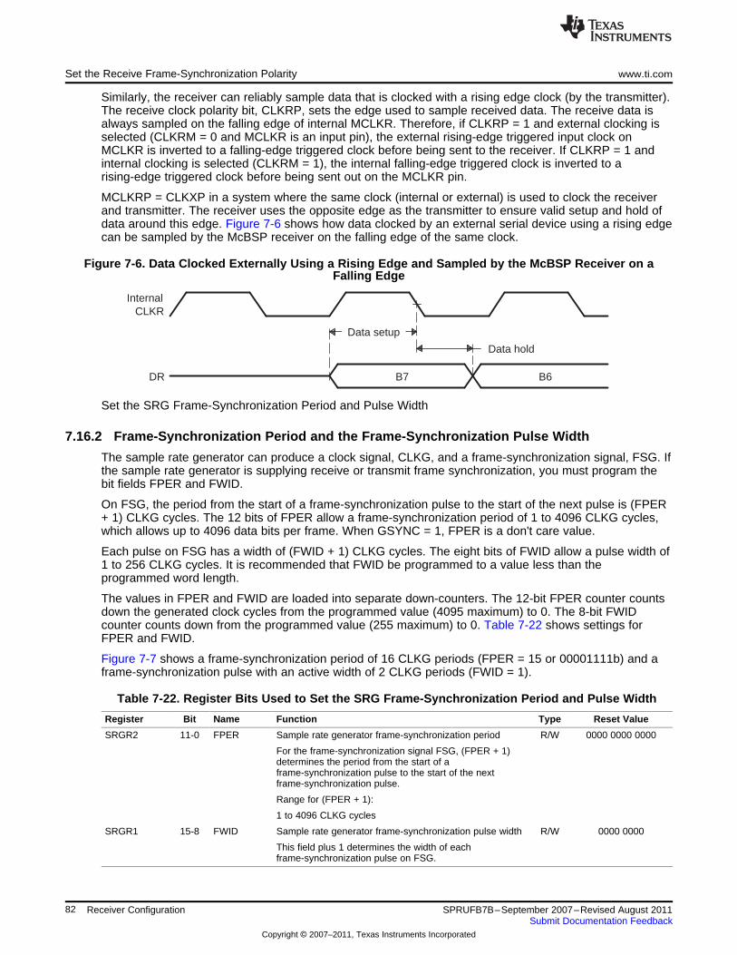
B6B7DR
CLKR
Data hold
ÁÁÁÁ Data setup
Internal
Set the Receive Frame-Synchronization Polarity www.ti.com
Similarly, the receiver can reliably sample data that is clocked with a rising edge clock (by the transmitter).The receive clock polarity bit, CLKRP, sets the edge used to sample received data. The receive data isalways sampled on the falling edge of internal MCLKR. Therefore, if CLKRP = 1 and external clocking isselected (CLKRM = 0 and MCLKR is an input pin), the external rising-edge triggered input clock onMCLKR is inverted to a falling-edge triggered clock before being sent to the receiver. If CLKRP = 1 andinternal clocking is selected (CLKRM = 1), the internal falling-edge triggered clock is inverted to arising-edge triggered clock before being sent out on the MCLKR pin.
MCLKRP = CLKXP in a system where the same clock (internal or external) is used to clock the receiverand transmitter. The receiver uses the opposite edge as the transmitter to ensure valid setup and hold ofdata around this edge. Figure 7-6 shows how data clocked by an external serial device using a rising edgecan be sampled by the McBSP receiver on the falling edge of the same clock.
Figure 7-6. Data Clocked Externally Using a Rising Edge and Sampled by the McBSP Receiver on aFalling Edge
Set the SRG Frame-Synchronization Period and Pulse Width
7.16.2 Frame-Synchronization Period and the Frame-Synchronization Pulse Width
The sample rate generator can produce a clock signal, CLKG, and a frame-synchronization signal, FSG. Ifthe sample rate generator is supplying receive or transmit frame synchronization, you must program thebit fields FPER and FWID.
On FSG, the period from the start of a frame-synchronization pulse to the start of the next pulse is (FPER+ 1) CLKG cycles. The 12 bits of FPER allow a frame-synchronization period of 1 to 4096 CLKG cycles,which allows up to 4096 data bits per frame. When GSYNC = 1, FPER is a don't care value.
Each pulse on FSG has a width of (FWID + 1) CLKG cycles. The eight bits of FWID allow a pulse width of1 to 256 CLKG cycles. It is recommended that FWID be programmed to a value less than theprogrammed word length.
The values in FPER and FWID are loaded into separate down-counters. The 12-bit FPER counter countsdown the generated clock cycles from the programmed value (4095 maximum) to 0. The 8-bit FWIDcounter counts down from the programmed value (255 maximum) to 0. Table 7-22 shows settings forFPER and FWID.
Figure 7-7 shows a frame-synchronization period of 16 CLKG periods (FPER = 15 or 00001111b) and aframe-synchronization pulse with an active width of 2 CLKG periods (FWID = 1).
Table 7-22. Register Bits Used to Set the SRG Frame-Synchronization Period and Pulse Width
Register Bit Name Function Type Reset Value
SRGR2 11-0 FPER Sample rate generator frame-synchronization period R/W 0000 0000 0000
For the frame-synchronization signal FSG, (FPER + 1)determines the period from the start of aframe-synchronization pulse to the start of the nextframe-synchronization pulse.
Range for (FPER + 1):
1 to 4096 CLKG cycles
SRGR1 15-8 FWID Sample rate generator frame-synchronization pulse width R/W 0000 0000
This field plus 1 determines the width of eachframe-synchronization pulse on FSG.
82 Receiver Configuration SPRUFB7B–September 2007–Revised August 2011Submit Documentation Feedback
Copyright © 2007–2011, Texas Instruments Incorporated
FSG
CLKG
19181716151413121110987654321
Frame-synchronization pulse width: (FWID + 1) x CLKG
Frame-synchronization period: (FPER+1) x CLKG
www.ti.com Set the Receive Clock Mode
Table 7-22. Register Bits Used to Set the SRG Frame-Synchronization Period and Pulse Width(continued)
Register Bit Name Function Type Reset Value
Range for (FWID + 1):
1 to 256 CLKG cycles
Figure 7-7. Frame of Period 16 CLKG Periods and Active Width of 2 CLKG Periods
When the sample rate generator comes out of reset, FSG is in its inactive state. Then, when GRST = 1and FSGM = 1, a frame-synchronization pulse is generated. The frame width value (FWID + 1) is counteddown on every CLKG cycle until it reaches 0, at which time FSG goes low. At the same time, the frameperiod value (FPER + 1) is also counting down. When this value reaches 0, FSG goes high, indicating anew frame.
7.17 Set the Receive Clock Mode
Table 7-23 shows the settings for bits used to set receive clock mode.
Table 7-23. Register Bits Used to Set the Receive Clock Mode
ResetRegister Bit Name Function Type Value
PCR 8 CLKRM Receive clock mode R/W 0
Case 1: Digital loopback mode not set (DLB = 0) in SPCR1.
CLKRM = 0 The MCLKR pin is an input pin that supplies theinternal receive clock (MCLKR).
CLKRM = 1 Internal MCLKR is driven by the sample rategenerator of the McBSP. The MCLKR pin is anoutput pin that reflects internal MCLKR.
Case 2: Digital loopback mode set (DLB = 1) in SPCR1.
CLKRM = 0 The MCLKR pin is in the high impedance state.The internal receive clock (MCLKR) is driven bythe internal transmit clock (CLKX). InternalCLKX is derived according to the CLKXM bit ofPCR.
CLKRM = 1 Internal MCLKR is driven by internal CLKX. TheMCLKR pin is an output pin that reflects internalMCLKR. Internal CLKX is derived according tothe CLKXM bit of PCR.
SPCR1 15 DLB Digital loopback mode R/W 00
DLB = 0 Digital loopback mode is disabled.
DLB = 1 Digital loopback mode is enabled. The receivesignals, including the receiveframe-synchronization signal, are connectedinternally through multiplexers to thecorresponding transmit signals.
83SPRUFB7B–September 2007–Revised August 2011 Receiver ConfigurationSubmit Documentation Feedback
Copyright © 2007–2011, Texas Instruments Incorporated
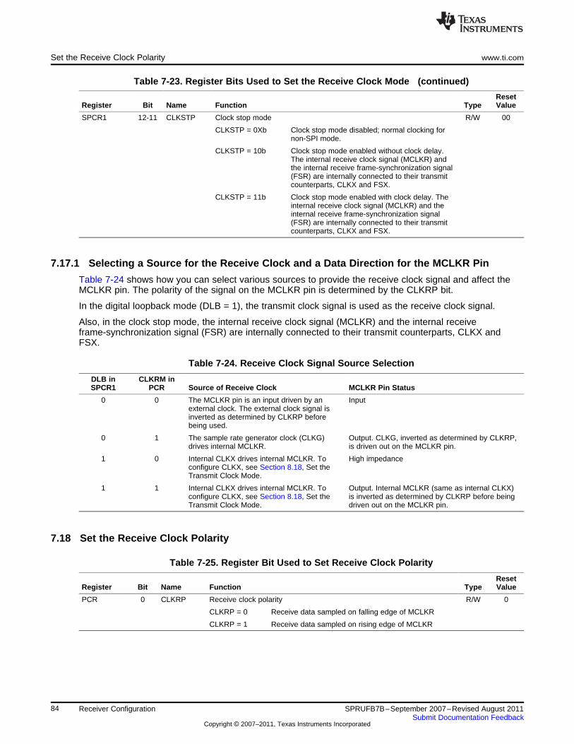
Set the Receive Clock Polarity www.ti.com
Table 7-23. Register Bits Used to Set the Receive Clock Mode (continued)
ResetRegister Bit Name Function Type Value
SPCR1 12-11 CLKSTP Clock stop mode R/W 00
CLKSTP = 0Xb Clock stop mode disabled; normal clocking fornon-SPI mode.
CLKSTP = 10b Clock stop mode enabled without clock delay.The internal receive clock signal (MCLKR) andthe internal receive frame-synchronization signal(FSR) are internally connected to their transmitcounterparts, CLKX and FSX.
CLKSTP = 11b Clock stop mode enabled with clock delay. Theinternal receive clock signal (MCLKR) and theinternal receive frame-synchronization signal(FSR) are internally connected to their transmitcounterparts, CLKX and FSX.
7.17.1 Selecting a Source for the Receive Clock and a Data Direction for the MCLKR Pin
Table 7-24 shows how you can select various sources to provide the receive clock signal and affect theMCLKR pin. The polarity of the signal on the MCLKR pin is determined by the CLKRP bit.
In the digital loopback mode (DLB = 1), the transmit clock signal is used as the receive clock signal.
Also, in the clock stop mode, the internal receive clock signal (MCLKR) and the internal receiveframe-synchronization signal (FSR) are internally connected to their transmit counterparts, CLKX andFSX.
Table 7-24. Receive Clock Signal Source Selection
DLB in CLKRM inSPCR1 PCR Source of Receive Clock MCLKR Pin Status
0 0 The MCLKR pin is an input driven by an Inputexternal clock. The external clock signal isinverted as determined by CLKRP beforebeing used.
0 1 The sample rate generator clock (CLKG) Output. CLKG, inverted as determined by CLKRP,drives internal MCLKR. is driven out on the MCLKR pin.
1 0 Internal CLKX drives internal MCLKR. To High impedanceconfigure CLKX, see Section 8.18, Set theTransmit Clock Mode.
1 1 Internal CLKX drives internal MCLKR. To Output. Internal MCLKR (same as internal CLKX)configure CLKX, see Section 8.18, Set the is inverted as determined by CLKRP before beingTransmit Clock Mode. driven out on the MCLKR pin.
7.18 Set the Receive Clock Polarity
Table 7-25. Register Bit Used to Set Receive Clock Polarity
ResetRegister Bit Name Function Type Value
PCR 0 CLKRP Receive clock polarity R/W 0
CLKRP = 0 Receive data sampled on falling edge of MCLKR
CLKRP = 1 Receive data sampled on rising edge of MCLKR
84 Receiver Configuration SPRUFB7B–September 2007–Revised August 2011Submit Documentation Feedback
Copyright © 2007–2011, Texas Instruments Incorporated
B6B7DR
CLKR
Data holdÁÁÁÁ Data setup
Internal
www.ti.com Set the SRG Clock Divide-Down Value
7.18.1 Frame Synchronization Pulses, Clock Signals, and Their Polarities
Receive frame-synchronization pulses can be generated internally by the sample rate generator (seeSection 3.2) or driven by an external source. The source of frame synchronization is selected byprogramming the mode bit, FSRM, in PCR. FSR is also affected by the GSYNC bit in SRGR2. Forinformation about the effects of FSRM and GSYNC, see Section 7.15, Set the ReceiveFrame-Synchronization Mode. Similarly, receive clocks can be selected to be inputs or outputs byprogramming the mode bit, CLKRM, in the PCR (see Section 7.17, Set the Receive Clock Mode).
When FSR and FSX are inputs (FSXM = FSRM= 0, external frame-synchronization pulses), the McBSPdetects them on the internal falling edge of clock, internal MCLKR, and internal CLKX, respectively. Thereceive data arriving at the DR pin is also sampled on the falling edge of internal MCLKR. These internalclock signals are either derived from external source via CLK(R/X) pins or driven by the sample rategenerator clock (CLKG) internal to the McBSP.
When FSR and FSX are outputs, implying that they are driven by the sample rate generator, they aregenerated (transition to their active state) on the rising edge of internal clock, CLK(R/X). Similarly, data onthe DX pin is output on the rising edge of internal CLKX.
FSRP, FSXP, CLKRP, and CLKXP in the pin control register (PCR) configure the polarities of the FSR,FSX, MCLKR, and CLKX signals, respectively. All frame-synchronization signals (internal FSR, internalFSX) that are internal to the serial port are active high. If the serial port is configured for external framesynchronization (FSR/FSX are inputs to McBSP) and FSRP = FSXP = 1, the external active-lowframe-synchronization signals are inverted before being sent to the receiver (internal FSR) and transmitter(internal FSX). Similarly, if internal synchronization (FSR/FSX are output pins and GSYNC = 0) isselected, the internal active-high frame-synchronization signals are inverted, if the polarity bit FS(R/X)P =1, before being sent to the FS(R/X) pin.
On the transmit side, the transmit clock polarity bit, CLKXP, sets the edge used to shift and clock outtransmit data. Data is always transmitted on the rising edge of internal CLKX. If CLKXP = 1 and externalclocking is selected (CLKXM = 0 and CLKX is an input), the external falling-edge triggered input clock onCLKX is inverted to a rising-edge triggered clock before being sent to the transmitter. If CLKXP = 1 andinternal clocking is selected (CLKXM = 1 and CLKX is an output pin), the internal (rising-edge triggered)clock, internal CLKX, is inverted before being sent out on the MCLKX pin.
Similarly, the receiver can reliably sample data that is clocked with a rising edge clock (by the transmitter).The receive clock polarity bit, CLKRP, sets the edge used to sample received data. The receive data isalways sampled on the falling edge of internal MCLKR. Therefore, if CLKRP = 1 and external clocking isselected (CLKRM = 0 and MCLKR is an input pin), the external rising-edge triggered input clock onMCLKR is inverted to a falling-edge triggered clock before being sent to the receiver. If CLKRP = 1 andinternal clocking is selected (CLKRM = 1), the internal falling-edge triggered clock is inverted to arising-edge triggered clock before being sent out on the MCLKR pin.
CLKRP = CLKXP in a system where the same clock (internal or external) is used to clock the receiver andtransmitter. The receiver uses the opposite edge as the transmitter to ensure valid setup and hold of dataaround this edge. Figure 7-8 shows how data clocked by an external serial device using a rising edge canbe sampled by the McBSP receiver on the falling edge of the same clock.
Figure 7-8. Data Clocked Externally Using a Rising Edge and Sampled by the McBSP Receiver on aFalling Edge
7.19 Set the SRG Clock Divide-Down Value
85SPRUFB7B–September 2007–Revised August 2011 Receiver ConfigurationSubmit Documentation Feedback
Copyright © 2007–2011, Texas Instruments Incorporated
Set the SRG Clock Synchronization Mode www.ti.com
Table 7-26. Register Bits Used to Set the Sample Rate Generator (SRG) Clock Divide-Down Value
Register Bit Name Function Type Reset Value
SRGR1 7-0 CLKGDV Sample rate generator clock divide-down value R/W 0000 0001
The input clock of the sample rate generator is divided by(CLKGDV + 1) to generate the required sample rate generatorclock frequency. The default value of CLKGDV is 1 (divide inputclock by 2).
7.19.1 Sample Rate Generator Clock Divider
The first divider stage generates the serial data bit clock from the input clock. This divider stage utilizes acounter, preloaded by CLKGDV, that contains the divide ratio value.
The output of the first divider stage is the data bit clock, which is output as CLKG and which serves as theinput for the second and third stages of the divider.
CLKG has a frequency equal to 1/(CLKGDV + 1) of sample rate generator input clock. Thus, the samplegenerator input clock frequency is divided by a value between 1 and 256. When CLKGDV is odd or equalto 0, the CLKG duty cycle is 50%. When CLKGDV is an even value, 2p, representing an odd divide-down,the high-state duration is p + 1 cycles and the low-state duration is p cycles.
7.20 Set the SRG Clock Synchronization Mode
For more details on using the clock synchronization feature, see Section 3.3, Synchronizing Sample RateGenerator Outputs to an External Clock.
Table 7-27. Register Bit Used to Set the SRG Clock Synchronization Mode
ResetRegister Bit Name Function Type Value
SRGR2 15 GSYNC Sample rate generator clock synchronization R/W 0
GSYNC is used only when the input clock source for the sample rategenerator is external—on the MCLKR or MCLKX pin.
GSYNC = 0 The sample rate generator clock (CLKG) is freerunning. CLKG oscillates without adjustment, andFSG pulses every (FPER + 1) CLKG cycles.
GSYNC = 1 Clock synchronization is performed. When apulse is detected on the FSR pin:• CLKG is adjusted as necessary so that it is
synchronized with the input clock on theMCLKR or MCLKX pin.
• FSG pulses. FSG only pulses in response toa pulse on the FSR pin. Theframe-synchronization period defined inFPER is ignored.
7.21 Set the SRG Clock Mode (Choose an Input Clock)
Table 7-28. Register Bits Used to Set the SRG Clock Mode (Choose an Input Clock)
ResetRegister Bit Name Function Type Value
PCR 7 SCLKME Sample rate generator clock mode R/W 0
SRGR2 13 CLKSM R/W 1
SCLKME = 0Reserved
CLKSM = 0
SCLKME = 0 Sample rate generator clock derived fromLSPCLK (default)
CLKSM = 1
86 Receiver Configuration SPRUFB7B–September 2007–Revised August 2011Submit Documentation Feedback
Copyright © 2007–2011, Texas Instruments Incorporated
www.ti.com Set the SRG Clock Mode (Choose an Input Clock)
Table 7-28. Register Bits Used to Set the SRG Clock Mode (Choose an Input Clock) (continued)
ResetRegister Bit Name Function Type Value
SCLKME = 1 Sample rate generator clock derived from MCLKRpinCLKSM = 0
SCLKME = 1 Sample rate generator clock derived from MCLKXpinCLKSM = 1
7.21.1 SRG Clock Mode
The sample rate generator can produce a clock signal (CLKG) for use by the receiver, the transmitter, orboth, but CLKG is derived from an input clock. Table 7-28 shows the four possible sources of the inputclock. For more details on generating CLKG, see Section 3.1.1, Clock Generation in the Sample RateGenerator.
87SPRUFB7B–September 2007–Revised August 2011 Receiver ConfigurationSubmit Documentation Feedback
Copyright © 2007–2011, Texas Instruments Incorporated
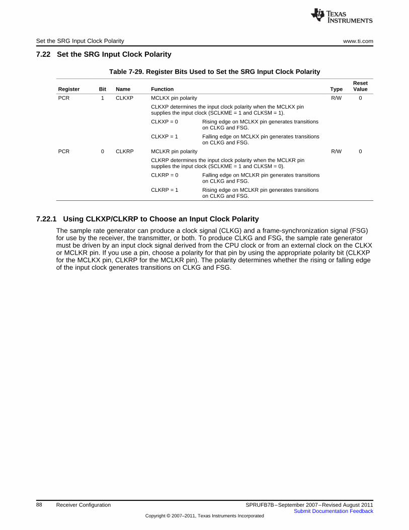
Set the SRG Input Clock Polarity www.ti.com
7.22 Set the SRG Input Clock Polarity
Table 7-29. Register Bits Used to Set the SRG Input Clock Polarity
ResetRegister Bit Name Function Type Value
PCR 1 CLKXP MCLKX pin polarity R/W 0
CLKXP determines the input clock polarity when the MCLKX pinsupplies the input clock (SCLKME = 1 and CLKSM = 1).
CLKXP = 0 Rising edge on MCLKX pin generates transitionson CLKG and FSG.
CLKXP = 1 Falling edge on MCLKX pin generates transitionson CLKG and FSG.
PCR 0 CLKRP MCLKR pin polarity R/W 0
CLKRP determines the input clock polarity when the MCLKR pinsupplies the input clock (SCLKME = 1 and CLKSM = 0).
CLKRP = 0 Falling edge on MCLKR pin generates transitionson CLKG and FSG.
CLKRP = 1 Rising edge on MCLKR pin generates transitionson CLKG and FSG.
7.22.1 Using CLKXP/CLKRP to Choose an Input Clock Polarity
The sample rate generator can produce a clock signal (CLKG) and a frame-synchronization signal (FSG)for use by the receiver, the transmitter, or both. To produce CLKG and FSG, the sample rate generatormust be driven by an input clock signal derived from the CPU clock or from an external clock on the CLKXor MCLKR pin. If you use a pin, choose a polarity for that pin by using the appropriate polarity bit (CLKXPfor the MCLKX pin, CLKRP for the MCLKR pin). The polarity determines whether the rising or falling edgeof the input clock generates transitions on CLKG and FSG.
88 Receiver Configuration SPRUFB7B–September 2007–Revised August 2011Submit Documentation Feedback
Copyright © 2007–2011, Texas Instruments Incorporated
Chapter 8SPRUFB7B–September 2007–Revised August 2011
Transmitter Configuration
To configure the McBSP transmitter, perform the following procedure:
1. Place the McBSP/transmitter in reset (see Section 8.2).
2. Program the McBSP registers for the desired transmitter operation (see Section 8.1).
3. Take the transmitter out of reset (see Section 8.2).
Topic ........................................................................................................................... Page
8.1 Programming the McBSP Registers for the Desired Transmitter Operation .............. 908.2 Resetting and Enabling the Transmitter ............................................................... 908.3 Set the Transmitter Pins to Operate as McBSP Pins .............................................. 918.4 Enable/Disable the Digital Loopback Mode ........................................................... 918.5 Enable/Disable the Clock Stop Mode ................................................................... 928.6 Enable/Disable Transmit Multichannel Selection ................................................... 938.7 Choose One or Two Phases for the Transmit Frame .............................................. 948.8 Set the Transmit Word Length(s) ......................................................................... 948.9 Set the Transmit Frame Length ........................................................................... 958.10 Enable/Disable the Transmit Frame-Synchronization Ignore Function ..................... 968.11 Set the Transmit Companding Mode .................................................................... 978.12 Set the Transmit Data Delay ............................................................................... 988.13 Set the Transmit DXENA Mode .......................................................................... 1008.14 Set the Transmit Interrupt Mode ........................................................................ 1008.15 Set the Transmit Frame-Synchronization Mode ................................................... 1018.16 Set the Transmit Frame-Synchronization Polarity ................................................ 1028.17 Set the SRG Frame-Synchronization Period and Pulse Width ............................... 1038.18 Set the Transmit Clock Mode ............................................................................ 1048.19 Set the Transmit Clock Polarity ......................................................................... 104
89SPRUFB7B–September 2007–Revised August 2011 Transmitter ConfigurationSubmit Documentation Feedback
Copyright © 2007–2011, Texas Instruments Incorporated
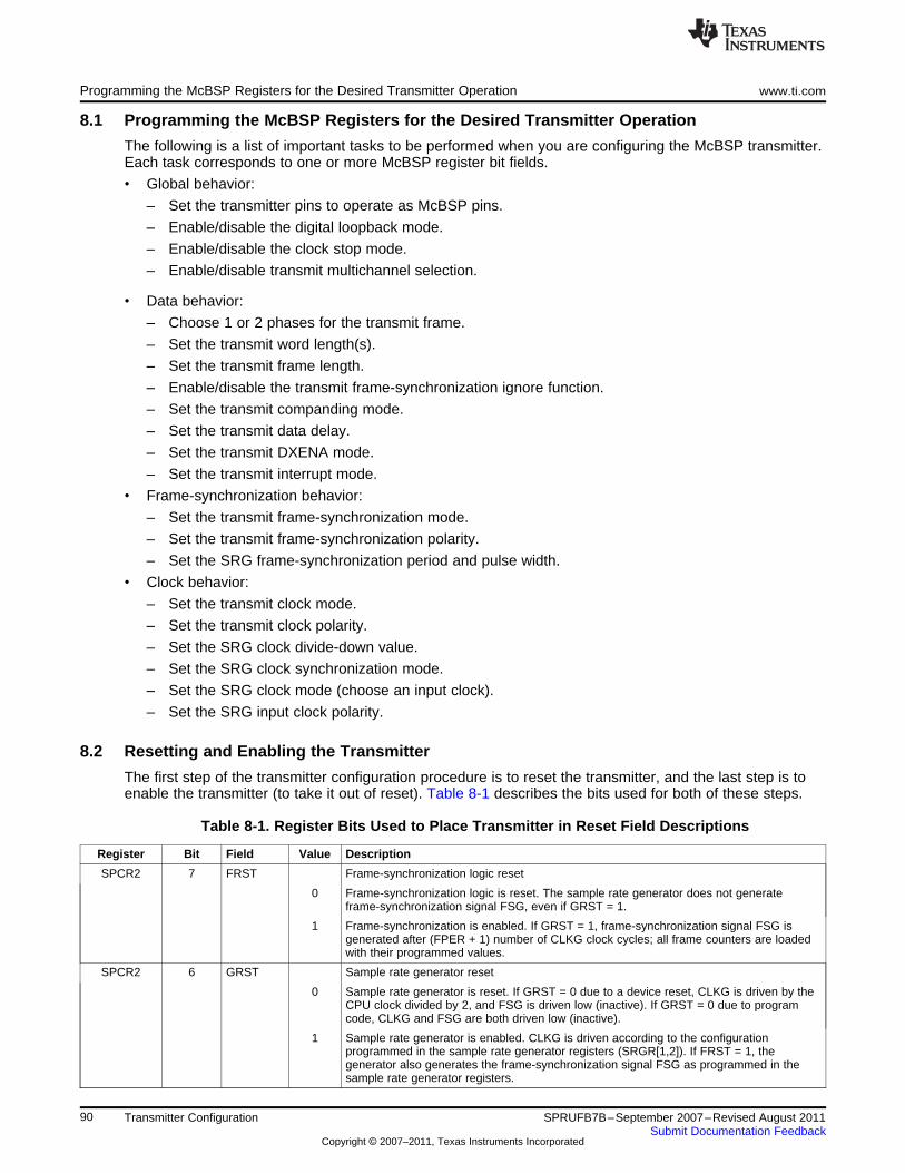
Programming the McBSP Registers for the Desired Transmitter Operation www.ti.com
8.1 Programming the McBSP Registers for the Desired Transmitter Operation
The following is a list of important tasks to be performed when you are configuring the McBSP transmitter.Each task corresponds to one or more McBSP register bit fields.
• Global behavior:
– Set the transmitter pins to operate as McBSP pins.
– Enable/disable the digital loopback mode.
– Enable/disable the clock stop mode.
– Enable/disable transmit multichannel selection.
• Data behavior:
– Choose 1 or 2 phases for the transmit frame.
– Set the transmit word length(s).
– Set the transmit frame length.
– Enable/disable the transmit frame-synchronization ignore function.
– Set the transmit companding mode.
– Set the transmit data delay.
– Set the transmit DXENA mode.
– Set the transmit interrupt mode.
• Frame-synchronization behavior:
– Set the transmit frame-synchronization mode.
– Set the transmit frame-synchronization polarity.
– Set the SRG frame-synchronization period and pulse width.
• Clock behavior:
– Set the transmit clock mode.
– Set the transmit clock polarity.
– Set the SRG clock divide-down value.
– Set the SRG clock synchronization mode.
– Set the SRG clock mode (choose an input clock).
– Set the SRG input clock polarity.
8.2 Resetting and Enabling the Transmitter
The first step of the transmitter configuration procedure is to reset the transmitter, and the last step is toenable the transmitter (to take it out of reset). Table 8-1 describes the bits used for both of these steps.
Table 8-1. Register Bits Used to Place Transmitter in Reset Field Descriptions
Register Bit Field Value Description
SPCR2 7 FRST Frame-synchronization logic reset
0 Frame-synchronization logic is reset. The sample rate generator does not generateframe-synchronization signal FSG, even if GRST = 1.
1 Frame-synchronization is enabled. If GRST = 1, frame-synchronization signal FSG isgenerated after (FPER + 1) number of CLKG clock cycles; all frame counters are loadedwith their programmed values.
SPCR2 6 GRST Sample rate generator reset
0 Sample rate generator is reset. If GRST = 0 due to a device reset, CLKG is driven by theCPU clock divided by 2, and FSG is driven low (inactive). If GRST = 0 due to programcode, CLKG and FSG are both driven low (inactive).
1 Sample rate generator is enabled. CLKG is driven according to the configurationprogrammed in the sample rate generator registers (SRGR[1,2]). If FRST = 1, thegenerator also generates the frame-synchronization signal FSG as programmed in thesample rate generator registers.
90 Transmitter Configuration SPRUFB7B–September 2007–Revised August 2011Submit Documentation Feedback
Copyright © 2007–2011, Texas Instruments Incorporated
www.ti.com Set the Transmitter Pins to Operate as McBSP Pins
Table 8-1. Register Bits Used to Place Transmitter in Reset Field Descriptions (continued)
Register Bit Field Value Description
SPCR2 0 XRST Transmitter reset
0 The serial port transmitter is disabled and in the reset state.
1 The serial port transmitter is enabled.
8.2.1 Reset Considerations
The serial port can be reset in the following two ways:
1. A DSP reset (XRS signal driven low) places the receiver, transmitter, and sample rate generator inreset. When the device reset is removed, GRST = FRST = RRST = XRST = 0, keeping the entireserial port in the reset state.
2. The serial port transmitter and receiver can be reset directly using the RRST and XRST bits in theserial port control registers. The sample rate generator can be reset directly using the GRST bit inSPCR2.
3. When using the DMA, the order in which McBSP events must occur is important. DMA channel andperipheral interrupts must be configured prior to releasing the McBSP transmitter from reset.
The reason for this is that an XRDY is fired when XRST = 1. The XRDY signals the DMA to startcopying data from the buffer into the transmit register. If the McBSP transmitter is released from resetbefore the DMA channel and peripheral interrupts are configured, the XRDY signals before the DMAchannel can receive the signal; therefore, the DMA does not move the data from the buffer to thetransmit register. The DMA PERINTFLG is edge-sensitive and will fail to recognize the XRDY, which iscontinuously high.
For more details about McBSP reset conditions and effects, see Section 9.2, Resetting and Initializing aMcBSP.
8.3 Set the Transmitter Pins to Operate as McBSP Pins
To configure a pin for its McBSP function , you should configure the bits of the GPxMUXn registerappropriately. In addition to this, bits 12 and 13 of the PCR register must be set to 0. These bits aredefined as reserved.
8.4 Enable/Disable the Digital Loopback Mode
The DLB bit determines whether the digital loopback mode is on. DLB is described in Table 8-2.
Table 8-2. Register Bit Used to Enable/Disable the Digital Loopback Mode
ResetRegister Bit Name Function Type Value
SPCR1 15 DLB Digital loopback mode R/W 0
DLB = 0 Digital loopback mode is disabled.
DLB = 1 Digital loopback mode is enabled.
8.4.1 Digital Loopback Mode
In the digital loopback mode, the receive signals are connected internally through multiplexers to thecorresponding transmit signals, as shown in Table 8-3. This mode allows testing of serial port code with asingle DSP device; the McBSP receives the data it transmits.
Table 8-3. Receive Signals Connected to Transmit Signals in Digital Loopback Mode
Is Fed Internally byThis Receive Signal This Transmit Signal
DR (receive data) DX (transmit data)
FSR (receive frame synchronization) FSX (transmit frame synchronization)
91SPRUFB7B–September 2007–Revised August 2011 Transmitter ConfigurationSubmit Documentation Feedback
Copyright © 2007–2011, Texas Instruments Incorporated
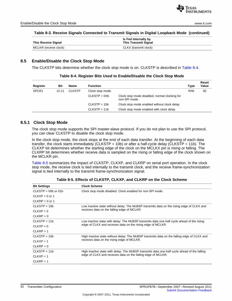
Enable/Disable the Clock Stop Mode www.ti.com
Table 8-3. Receive Signals Connected to Transmit Signals in Digital Loopback Mode (continued)
Is Fed Internally byThis Receive Signal This Transmit Signal
MCLKR (receive clock) CLKX (transmit clock)
8.5 Enable/Disable the Clock Stop Mode
The CLKSTP bits determine whether the clock stop mode is on. CLKSTP is described in Table 8-4.
Table 8-4. Register Bits Used to Enable/Disable the Clock Stop Mode
ResetRegister Bit Name Function Type Value
SPCR1 12-11 CLKSTP Clock stop mode R/W 00
CLKSTP = 0Xb Clock stop mode disabled; normal clocking fornon-SPI mode.
CLKSTP = 10b Clock stop mode enabled without clock delay
CLKSTP = 11b Clock stop mode enabled with clock delay
8.5.1 Clock Stop Mode
The clock stop mode supports the SPI master-slave protocol. If you do not plan to use the SPI protocol,you can clear CLKSTP to disable the clock stop mode.
In the clock stop mode, the clock stops at the end of each data transfer. At the beginning of each datatransfer, the clock starts immediately (CLKSTP = 10b) or after a half-cycle delay (CLKSTP = 11b). TheCLKXP bit determines whether the starting edge of the clock on the MCLKX pin is rising or falling. TheCLKRP bit determines whether receive data is sampled on the rising or falling edge of the clock shown onthe MCLKR pin.
Table 8-5 summarizes the impact of CLKSTP, CLKXP, and CLKRP on serial port operation. In the clockstop mode, the receive clock is tied internally to the transmit clock, and the receive frame-synchronizationsignal is tied internally to the transmit frame-synchronization signal.
Table 8-5. Effects of CLKSTP, CLKXP, and CLKRP on the Clock Scheme
Bit Settings Clock Scheme
CLKSTP = 00b or 01b Clock stop mode disabled. Clock enabled for non-SPI mode.
CLKXP = 0 or 1
CLKRP = 0 or 1
CLKSTP = 10b Low inactive state without delay: The McBSP transmits data on the rising edge of CLKX andreceives data on the falling edge of MCLKR.CLKXP = 0
CLKRP = 0
CLKSTP = 11b Low inactive state with delay: The McBSP transmits data one-half cycle ahead of the risingedge of CLKX and receives data on the rising edge of MCLKR.CLKXP = 0
CLKRP = 1
CLKSTP = 10b High inactive state without delay: The McBSP transmits data on the falling edge of CLKX andreceives data on the rising edge of MCLKR.CLKXP = 1
CLKRP = 0
CLKSTP = 11b High inactive state with delay: The McBSP transmits data one-half cycle ahead of the fallingedge of CLKX and receives data on the falling edge of MCLKR.CLKXP = 1
CLKRP = 1
92 Transmitter Configuration SPRUFB7B–September 2007–Revised August 2011Submit Documentation Feedback
Copyright © 2007–2011, Texas Instruments Incorporated
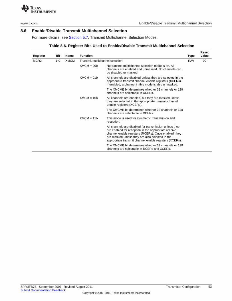
www.ti.com Enable/Disable Transmit Multichannel Selection
8.6 Enable/Disable Transmit Multichannel Selection
For more details, see Section 5.7, Transmit Multichannel Selection Modes.
Table 8-6. Register Bits Used to Enable/Disable Transmit Multichannel Selection
ResetRegister Bit Name Function Type Value
MCR2 1-0 XMCM Transmit multichannel selection R/W 00
XMCM = 00b No transmit multichannel selection mode is on. Allchannels are enabled and unmasked. No channels canbe disabled or masked.
XMCM = 01b All channels are disabled unless they are selected in theappropriate transmit channel enable registers (XCERs).If enabled, a channel in this mode is also unmasked.
The XMCME bit determines whether 32 channels or 128channels are selectable in XCERs.
XMCM = 10b All channels are enabled, but they are masked unlessthey are selected in the appropriate transmit channelenable registers (XCERs).
The XMCME bit determines whether 32 channels or 128channels are selectable in XCERs.
XMCM = 11b This mode is used for symmetric transmission andreception.
All channels are disabled for transmission unless theyare enabled for reception in the appropriate receivechannel enable registers (RCERs). Once enabled, theyare masked unless they are also selected in theappropriate transmit channel enable registers (XCERs).
The XMCME bit determines whether 32 channels or 128channels are selectable in RCERs and XCERs.
93SPRUFB7B–September 2007–Revised August 2011 Transmitter ConfigurationSubmit Documentation Feedback
Copyright © 2007–2011, Texas Instruments Incorporated
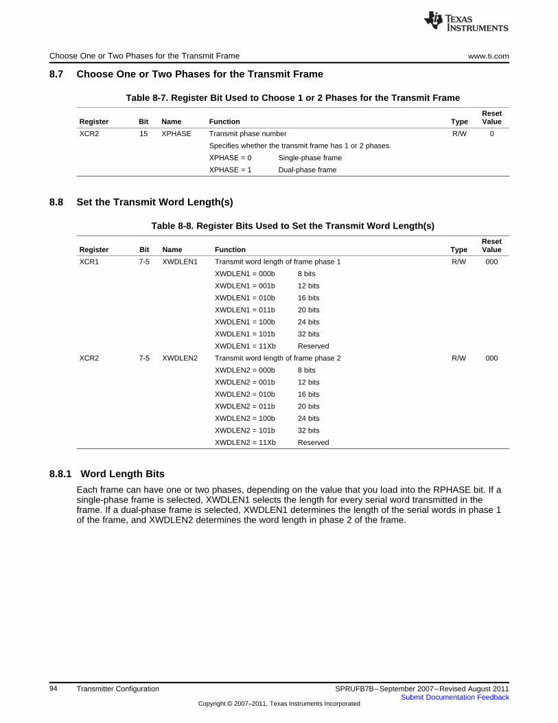
Choose One or Two Phases for the Transmit Frame www.ti.com
8.7 Choose One or Two Phases for the Transmit Frame
Table 8-7. Register Bit Used to Choose 1 or 2 Phases for the Transmit Frame
ResetRegister Bit Name Function Type Value
XCR2 15 XPHASE Transmit phase number R/W 0
Specifies whether the transmit frame has 1 or 2 phases.
XPHASE = 0 Single-phase frame
XPHASE = 1 Dual-phase frame
8.8 Set the Transmit Word Length(s)
Table 8-8. Register Bits Used to Set the Transmit Word Length(s)
ResetRegister Bit Name Function Type Value
XCR1 7-5 XWDLEN1 Transmit word length of frame phase 1 R/W 000
XWDLEN1 = 000b 8 bits
XWDLEN1 = 001b 12 bits
XWDLEN1 = 010b 16 bits
XWDLEN1 = 011b 20 bits
XWDLEN1 = 100b 24 bits
XWDLEN1 = 101b 32 bits
XWDLEN1 = 11Xb Reserved
XCR2 7-5 XWDLEN2 Transmit word length of frame phase 2 R/W 000
XWDLEN2 = 000b 8 bits
XWDLEN2 = 001b 12 bits
XWDLEN2 = 010b 16 bits
XWDLEN2 = 011b 20 bits
XWDLEN2 = 100b 24 bits
XWDLEN2 = 101b 32 bits
XWDLEN2 = 11Xb Reserved
8.8.1 Word Length Bits
Each frame can have one or two phases, depending on the value that you load into the RPHASE bit. If asingle-phase frame is selected, XWDLEN1 selects the length for every serial word transmitted in theframe. If a dual-phase frame is selected, XWDLEN1 determines the length of the serial words in phase 1of the frame, and XWDLEN2 determines the word length in phase 2 of the frame.
94 Transmitter Configuration SPRUFB7B–September 2007–Revised August 2011Submit Documentation Feedback
Copyright © 2007–2011, Texas Instruments Incorporated
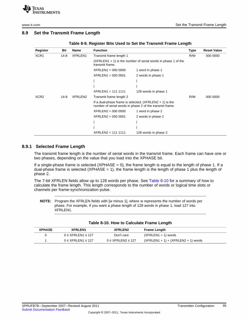
www.ti.com Set the Transmit Frame Length
8.9 Set the Transmit Frame Length
Table 8-9. Register Bits Used to Set the Transmit Frame Length
Register Bit Name Function Type Reset Value
XCR1 14-8 XFRLEN1 Transmit frame length 1 R/W 000 0000
(XFRLEN1 + 1) is the number of serial words in phase 1 of thetransmit frame.
XFRLEN1 = 000 0000 1 word in phase 1
XFRLEN1 = 000 0001 2 words in phase 1
| |
| |
XFRLEN1 = 111 1111 128 words in phase 1
XCR2 14-8 XFRLEN2 Transmit frame length 2 R/W 000 0000
If a dual-phase frame is selected, (XFRLEN2 + 1) is thenumber of serial words in phase 2 of the transmit frame.
XFRLEN2 = 000 0000 1 word in phase 2
XFRLEN2 = 000 0001 2 words in phase 2
| |
| |
XFRLEN2 = 111 1111 128 words in phase 2
8.9.1 Selected Frame Length
The transmit frame length is the number of serial words in the transmit frame. Each frame can have one ortwo phases, depending on the value that you load into the XPHASE bit.
If a single-phase frame is selected (XPHASE = 0), the frame length is equal to the length of phase 1. If adual-phase frame is selected (XPHASE = 1), the frame length is the length of phase 1 plus the length ofphase 2.
The 7-bit XFRLEN fields allow up to 128 words per phase. See Table 8-10 for a summary of how tocalculate the frame length. This length corresponds to the number of words or logical time slots orchannels per frame-synchronization pulse.
NOTE: Program the XFRLEN fields with [w minus 1], where w represents the number of words perphase. For example, if you want a phase length of 128 words in phase 1, load 127 intoXFRLEN1.
Table 8-10. How to Calculate Frame Length
XPHASE XFRLEN1 XFRLEN2 Frame Length
0 0 ≤ XFRLEN1 ≤ 127 Don't care (XFRLEN1 + 1) words
1 0 ≤ XFRLEN1 ≤ 127 0 ≤ XFRLEN2 ≤ 127 (XFRLEN1 + 1) + (XFRLEN2 + 1) words
95SPRUFB7B–September 2007–Revised August 2011 Transmitter ConfigurationSubmit Documentation Feedback
Copyright © 2007–2011, Texas Instruments Incorporated
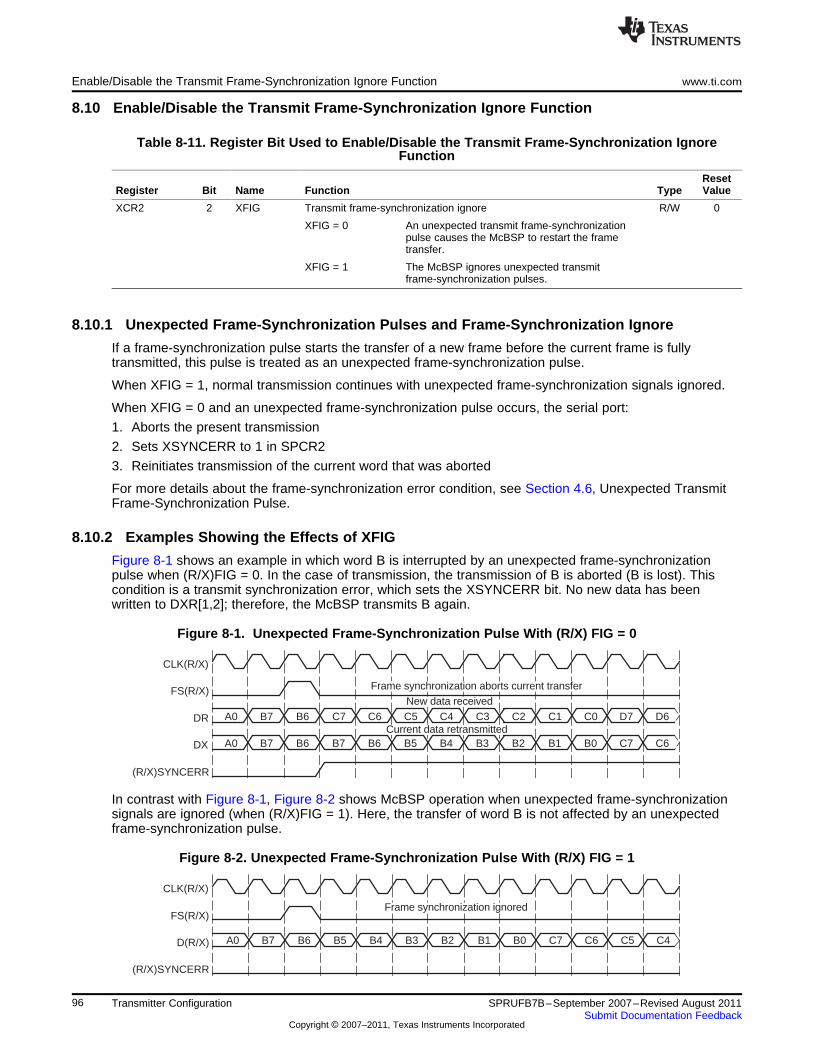
Current data retransmitted
New data received
(R/X)SYNCERR
DX
DR
FS(R/X)
CLK(R/X)
C6C7B0
ÁÁÁÁÁÁB2B3B4B5B7 B6B6B7A0 B1
D6D7C0C1C2C3C4C5C6C7B6B7A0
ÁÁÁÁÁÁÁÁFrame synchronization aborts current transfer
(R/X)SYNCERR
D(R/X)
FS(R/X)
CLK(R/X)
C4C5C6C7B0B1B2B3B4B5B6B7A0
ÁÁÁÁFrame synchronization ignored
Enable/Disable the Transmit Frame-Synchronization Ignore Function www.ti.com
8.10 Enable/Disable the Transmit Frame-Synchronization Ignore Function
Table 8-11. Register Bit Used to Enable/Disable the Transmit Frame-Synchronization IgnoreFunction
ResetRegister Bit Name Function Type Value
XCR2 2 XFIG Transmit frame-synchronization ignore R/W 0
XFIG = 0 An unexpected transmit frame-synchronizationpulse causes the McBSP to restart the frametransfer.
XFIG = 1 The McBSP ignores unexpected transmitframe-synchronization pulses.
8.10.1 Unexpected Frame-Synchronization Pulses and Frame-Synchronization Ignore
If a frame-synchronization pulse starts the transfer of a new frame before the current frame is fullytransmitted, this pulse is treated as an unexpected frame-synchronization pulse.
When XFIG = 1, normal transmission continues with unexpected frame-synchronization signals ignored.
When XFIG = 0 and an unexpected frame-synchronization pulse occurs, the serial port:
1. Aborts the present transmission
2. Sets XSYNCERR to 1 in SPCR2
3. Reinitiates transmission of the current word that was aborted
For more details about the frame-synchronization error condition, see Section 4.6, Unexpected TransmitFrame-Synchronization Pulse.
8.10.2 Examples Showing the Effects of XFIG
Figure 8-1 shows an example in which word B is interrupted by an unexpected frame-synchronizationpulse when (R/X)FIG = 0. In the case of transmission, the transmission of B is aborted (B is lost). Thiscondition is a transmit synchronization error, which sets the XSYNCERR bit. No new data has beenwritten to DXR[1,2]; therefore, the McBSP transmits B again.
Figure 8-1. Unexpected Frame-Synchronization Pulse With (R/X) FIG = 0
In contrast with Figure 8-1, Figure 8-2 shows McBSP operation when unexpected frame-synchronizationsignals are ignored (when (R/X)FIG = 1). Here, the transfer of word B is not affected by an unexpectedframe-synchronization pulse.
Figure 8-2. Unexpected Frame-Synchronization Pulse With (R/X) FIG = 1
96 Transmitter Configuration SPRUFB7B–September 2007–Revised August 2011Submit Documentation Feedback
Copyright © 2007–2011, Texas Instruments Incorporated
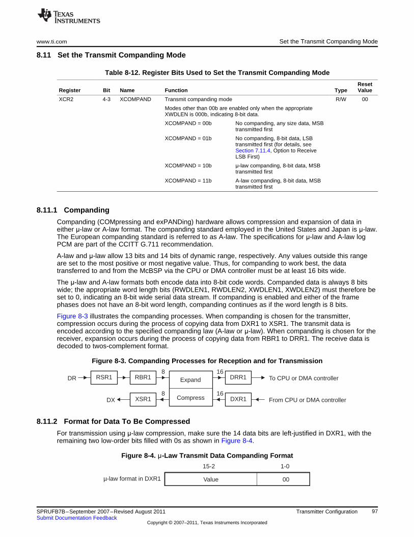
From CPU or DMA controllerDXR1
To CPU or DMA controllerDRR1
16
16
DX8
8
XSR1 Compress
ExpandDR RBR1RSR1
µ-law format in DXR1 00Value
1-015-2
www.ti.com Set the Transmit Companding Mode
8.11 Set the Transmit Companding Mode
Table 8-12. Register Bits Used to Set the Transmit Companding Mode
ResetRegister Bit Name Function Type Value
XCR2 4-3 XCOMPAND Transmit companding mode R/W 00
Modes other than 00b are enabled only when the appropriateXWDLEN is 000b, indicating 8-bit data.
XCOMPAND = 00b No companding, any size data, MSBtransmitted first
XCOMPAND = 01b No companding, 8-bit data, LSBtransmitted first (for details, seeSection 7.11.4, Option to ReceiveLSB First)
XCOMPAND = 10b μ-law companding, 8-bit data, MSBtransmitted first
XCOMPAND = 11b A-law companding, 8-bit data, MSBtransmitted first
8.11.1 Companding
Companding (COMpressing and exPANDing) hardware allows compression and expansion of data ineither μ-law or A-law format. The companding standard employed in the United States and Japan is μ-law.The European companding standard is referred to as A-law. The specifications for μ-law and A-law logPCM are part of the CCITT G.711 recommendation.
A-law and μ-law allow 13 bits and 14 bits of dynamic range, respectively. Any values outside this rangeare set to the most positive or most negative value. Thus, for companding to work best, the datatransferred to and from the McBSP via the CPU or DMA controller must be at least 16 bits wide.
The μ-law and A-law formats both encode data into 8-bit code words. Companded data is always 8 bitswide; the appropriate word length bits (RWDLEN1, RWDLEN2, XWDLEN1, XWDLEN2) must therefore beset to 0, indicating an 8-bit wide serial data stream. If companding is enabled and either of the framephases does not have an 8-bit word length, companding continues as if the word length is 8 bits.
Figure 8-3 illustrates the companding processes. When companding is chosen for the transmitter,compression occurs during the process of copying data from DXR1 to XSR1. The transmit data isencoded according to the specified companding law (A-law or μ-law). When companding is chosen for thereceiver, expansion occurs during the process of copying data from RBR1 to DRR1. The receive data isdecoded to twos-complement format.
Figure 8-3. Companding Processes for Reception and for Transmission
8.11.2 Format for Data To Be Compressed
For transmission using μ-law compression, make sure the 14 data bits are left-justified in DXR1, with theremaining two low-order bits filled with 0s as shown in Figure 8-4.
Figure 8-4. μ-Law Transmit Data Companding Format
97SPRUFB7B–September 2007–Revised August 2011 Transmitter ConfigurationSubmit Documentation Feedback
Copyright © 2007–2011, Texas Instruments Incorporated
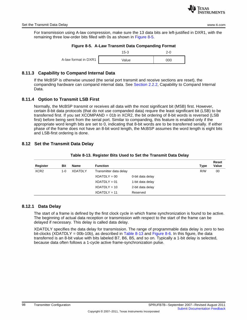
000
2-0
Value
15-3
A-law format in DXR1
Set the Transmit Data Delay www.ti.com
For transmission using A-law compression, make sure the 13 data bits are left-justified in DXR1, with theremaining three low-order bits filled with 0s as shown in Figure 8-5.
Figure 8-5. A-Law Transmit Data Companding Format
8.11.3 Capability to Compand Internal Data
If the McBSP is otherwise unused (the serial port transmit and receive sections are reset), thecompanding hardware can compand internal data. See Section 2.2.2, Capability to Compand InternalData.
8.11.4 Option to Transmit LSB First
Normally, the McBSP transmit or receives all data with the most significant bit (MSB) first. However,certain 8-bit data protocols (that do not use companded data) require the least significant bit (LSB) to betransferred first. If you set XCOMPAND = 01b in XCR2, the bit ordering of 8-bit words is reversed (LSBfirst) before being sent from the serial port. Similar to companding, this feature is enabled only if theappropriate word length bits are set to 0, indicating that 8-bit words are to be transferred serially. If eitherphase of the frame does not have an 8-bit word length, the McBSP assumes the word length is eight bitsand LSB-first ordering is done.
8.12 Set the Transmit Data Delay
Table 8-13. Register Bits Used to Set the Transmit Data Delay
ResetRegister Bit Name Function Type Value
XCR2 1-0 XDATDLY Transmitter data delay R/W 00
XDATDLY = 00 0-bit data delay
XDATDLY = 01 1-bit data delay
XDATDLY = 10 2-bit data delay
XDATDLY = 11 Reserved
8.12.1 Data Delay
The start of a frame is defined by the first clock cycle in which frame synchronization is found to be active.The beginning of actual data reception or transmission with respect to the start of the frame can bedelayed if necessary. This delay is called data delay.
XDATDLY specifies the data delay for transmission. The range of programmable data delay is zero to twobit-clocks (XDATDLY = 00b-10b), as described in Table 8-13 and Figure 8-6. In this figure, the datatransferred is an 8-bit value with bits labeled B7, B6, B5, and so on. Typically a 1-bit delay is selected,because data often follows a 1-cycle active frame-synchronization pulse.
98 Transmitter Configuration SPRUFB7B–September 2007–Revised August 2011Submit Documentation Feedback
Copyright © 2007–2011, Texas Instruments Incorporated
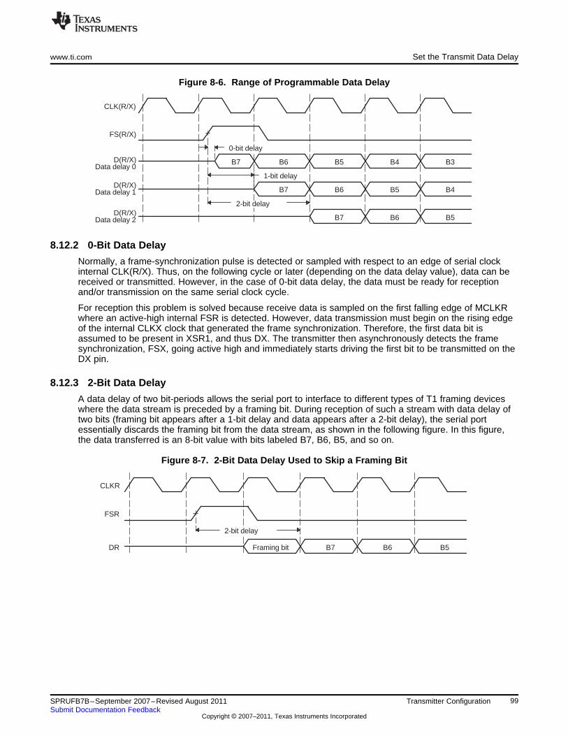
B5B6B7
B4B5B6B7
B3B4B5B6B7
Data delay 2D(R/X)
Data delay 1D(R/X)
Data delay 0D(R/X)
FS(R/X)
CLK(R/X)
1-bit delayÁÁÁÁÁÁÁÁÁÁÁÁÁÁÁÁÁÁÁÁ0-bit delay
2-bit delay
DR Framing bit B5B6B7
FSR
CLKR ÁÁÁÁ2-bit delay
www.ti.com Set the Transmit Data Delay
Figure 8-6. Range of Programmable Data Delay
8.12.2 0-Bit Data Delay
Normally, a frame-synchronization pulse is detected or sampled with respect to an edge of serial clockinternal CLK(R/X). Thus, on the following cycle or later (depending on the data delay value), data can bereceived or transmitted. However, in the case of 0-bit data delay, the data must be ready for receptionand/or transmission on the same serial clock cycle.
For reception this problem is solved because receive data is sampled on the first falling edge of MCLKRwhere an active-high internal FSR is detected. However, data transmission must begin on the rising edgeof the internal CLKX clock that generated the frame synchronization. Therefore, the first data bit isassumed to be present in XSR1, and thus DX. The transmitter then asynchronously detects the framesynchronization, FSX, going active high and immediately starts driving the first bit to be transmitted on theDX pin.
8.12.3 2-Bit Data Delay
A data delay of two bit-periods allows the serial port to interface to different types of T1 framing deviceswhere the data stream is preceded by a framing bit. During reception of such a stream with data delay oftwo bits (framing bit appears after a 1-bit delay and data appears after a 2-bit delay), the serial portessentially discards the framing bit from the data stream, as shown in the following figure. In this figure,the data transferred is an 8-bit value with bits labeled B7, B6, B5, and so on.
Figure 8-7. 2-Bit Data Delay Used to Skip a Framing Bit
99SPRUFB7B–September 2007–Revised August 2011 Transmitter ConfigurationSubmit Documentation Feedback
Copyright © 2007–2011, Texas Instruments Incorporated
Set the Transmit DXENA Mode www.ti.com
8.13 Set the Transmit DXENA Mode
Table 8-14. Register Bit Used to Set the Transmit DXENA (DX Delay Enabler) Mode
ResetRegister Bit Name Function Type Value
SPCR1 7 DXENA DX delay enabler mode R/W 0
DXENA = 0 DX delay enabler is off.
DXENA = 1 DX delay enabler is on.
8.13.1 DXENA Mode
The DXENA bit controls the delay enabler on the DX pin. Set DXENA to enable an extra delay for turn-ontime. This bit does not control the data itself, so only the first bit is delayed.
If you tie together the DX pins of multiple McBSPs, make sure DXENA = 1 to avoid having more than oneMcBSP transmit on the data line at one time.
8.14 Set the Transmit Interrupt Mode
The transmitter interrupt (XINT) signals the CPU of changes to the serial port status. Four options exist forconfiguring this interrupt. The options are set by the transmit interrupt mode bits, XINTM, in SPCR2.
Table 8-15. Register Bits Used to Set the Transmit Interrupt Mode
ResetRegister Bit Name Function Type Value
SPCR2 5-4 XINTM Transmit interrupt mode R/W 00
XINTM = 00 XINT generated when XRDY changes from 0 to 1.
XINTM = 01 XINT generated by an end-of-block or end-of-framecondition in a transmit multichannel selection mode. Inany of the transmit multichannel selection modes,interrupt after every 16-channel block boundary hasbeen crossed within a frame and at the end of the frame.For details, see Section 5.8, Using Interrupts BetweenBlock Transfers. In any other serial transfer case, thissetting is not applicable and, therefore, no interrupts aregenerated.
XINTM = 10 XINT generated by a new transmitframe-synchronization pulse. Interrupt on detection ofeach transmit frame-synchronization pulse. Thisgenerates an interrupt even when the transmitter is in itsreset state. This is done by synchronizing the incomingframe-synchronization pulse to the CPU clock andsending it to the CPU via XINT.
XINTM = 11 XINT generated when XSYNCERR is set. Interrupt onframe-synchronization error. Regardless of the value ofXINTM, XSYNCERR can be read to detect thiscondition. For more information on using XSYNCERR,see Section 4.6, Unexpected TransmitFrame-Synchronization Pulse.
100 Transmitter Configuration SPRUFB7B–September 2007–Revised August 2011Submit Documentation Feedback
Copyright © 2007–2011, Texas Instruments Incorporated
www.ti.com Set the Transmit Frame-Synchronization Mode
8.15 Set the Transmit Frame-Synchronization Mode
Table 8-16. Register Bits Used to Set the Transmit Frame-Synchronization Mode
ResetRegister Bit Name Function Type Value
PCR 11 FSXM Transmit frame-synchronization mode R/W 0
FSXM = 0 Transmit frame synchronization is supplied by anexternal source via the FSX pin.
FSXM = 1 Transmit frame synchronization is supplied by theMcBSP, as determined by the FSGM bit of SRGR2.
SRGR2 12 FSGM Sample rate generator transmit frame-synchronization mode R/W 0
Used when FSXM = 1 in PCR.
FSGM = 0 The McBSP generates a transmitframe-synchronization pulse when the content ofDXR[1,2] is copied to XSR[1,2].
FSGM = 1 The transmitter uses frame-synchronization pulsesgenerated by the sample rate generator. Program theFWID bits to set the width of each pulse. Program theFPER bits to set the frame-synchronization period.
8.15.1 Transmit Frame-Synchronization Modes
Table 8-17 shows how FSXM and FSGM select the source of transmit frame-synchronization pulses. Thethree choices are:
• External frame-synchronization input
• Sample rate generator frame-synchronization signal (FSG)
• Internal signal that indicates a DXR-to-XSR copy has been made
Table 8-17 also shows the effect of each bit setting on the FSX pin. The polarity of the signal on the FSXpin is determined by the FSXP bit.
Table 8-17. How FSXM and FSGM Select the Source of Transmit Frame-Synchronization Pulses
Source of Transmit FrameFSXM FSGM Synchronization FSX Pin Status
0 0 or 1 An external frame-synchronization signal enters the InputMcBSP through the FSX pin. The signal is theninverted by FSXP before being used as internal FSX.
1 1 Internal FSX is driven by the sample rate generator Output. FSG is inverted by FSXP before being drivenframe-synchronization signal (FSG). out on FSX pin.
1 0 A DXR-to-XSR copy causes the McBSP to generate a Output. The generated frame-synchronization pulse istransmit frame-synchronization pulse that is 1 cycle inverted as determined by FSXP before being drivenwide. out on FSX pin.
8.15.2 Other Considerations
If the sample rate generator creates a frame-synchronization signal (FSG) that is derived from an externalinput clock, the GSYNC bit determines whether FSG is kept synchronized with pulses on the FSR pin. Formore details, see Section 3.3, Synchronizing Sample Rate Generator Outputs to an External Clock.
In the clock stop mode (CLKSTP = 10b or 11b), the McBSP can act as a master or as a slave in the SPIprotocol. If the McBSP is a master and must provide a slave-enable signal (SPISTE) on the FSX pin,make sure that FSXM = 1 and FSGM = 0 so that FSX is an output and is driven active for the duration ofeach transmission. If the McBSP is a slave, make sure that FSXM = 0 so that the McBSP can receive theslave-enable signal on the FSX pin.
101SPRUFB7B–September 2007–Revised August 2011 Transmitter ConfigurationSubmit Documentation Feedback
Copyright © 2007–2011, Texas Instruments Incorporated
Set the Transmit Frame-Synchronization Polarity www.ti.com
8.16 Set the Transmit Frame-Synchronization Polarity
Table 8-18. Register Bit Used to Set Transmit Frame-Synchronization Polarity
ResetRegister Bit Name Function Type Value
PCR 3 FSXP Transmit frame-synchronization polarity R/W 0
FSXP = 0 Frame-synchronization pulse FSX is active high.
FSXP = 1 Frame-synchronization pulse FSX is active low.
8.16.1 Frame Synchronization Pulses, Clock Signals, and Their Polarities
Transmit frame-synchronization pulses can be generated internally by the sample rate generator (seeSection 3.2) or driven by an external source. The source of frame synchronization is selected byprogramming the mode bit, FSXM, in PCR. FSX is also affected by the FSGM bit in SRGR2. Forinformation about the effects of FSXM and FSGM, see Section 8.15, Set the TransmitFrame-Synchronization Mode). Similarly, transmit clocks can be selected to be inputs or outputs byprogramming the mode bit, CLKXM, in the PCR (see Section 8.18, Set the Transmit Clock Mode).
When FSR and FSX are inputs (FSXM = FSRM= 0, external frame-synchronization pulses), the McBSPdetects them on the internal falling edge of clock, internal MCLKR, and internal CLKX, respectively. Thereceive data arriving at the DR pin is also sampled on the falling edge of internal MCLKR. These internalclock signals are either derived from external source via CLK(R/X) pins or driven by the sample rategenerator clock (CLKG) internal to the McBSP.
When FSR and FSX are outputs, implying that they are driven by the sample rate generator, they aregenerated (transition to their active state) on the rising edge of internal clock, CLK(R/X). Similarly, data onthe DX pin is output on the rising edge of internal CLKX.
FSRP, FSXP, CLKRP, and CLKXP in the pin control register (PCR) configure the polarities of the FSR,FSX, MCLKR, and CLKX signals, respectively. All frame-synchronization signals (internal FSR, internalFSX) that are internal to the serial port are active high. If the serial port is configured for external framesynchronization (FSR/FSX are inputs to McBSP) and FSRP = FSXP = 1, the external active-lowframe-synchronization signals are inverted before being sent to the receiver (internal FSR) and transmitter(internal FSX). Similarly, if internal synchronization (FSR/FSX are output pins and GSYNC = 0) is selectedand the polarity bit FS(R/X)P = 1, the internal active-high frame-synchronization signals are invertedbefore being sent to the FS(R/X) pin.
On the transmit side, the transmit clock polarity bit, CLKXP, sets the edge used to shift and clock outtransmit data. Data is always transmitted on the rising edge of internal CLKX. If CLKXP = 1 and externalclocking is selected (CLKXM = 0 and CLKX is an input), the external falling-edge triggered input clock onCLKX is inverted to a rising-edge triggered clock before being sent to the transmitter. If CLKXP = 1, andinternal clocking selected (CLKXM = 1 and CLKX is an output pin), the internal (rising-edge triggered)clock, internal CLKX, is inverted before being sent out on the MCLKX pin.
Similarly, the receiver can reliably sample data that is clocked with a rising edge clock (by the transmitter).The receive clock polarity bit, CLKRP, sets the edge used to sample received data. The receive data isalways sampled on the falling edge of internal MCLKR. Therefore, if CLKRP = 1 and external clocking isselected (CLKRM = 0 and MCLKR is an input pin), the external rising-edge triggered input clock onMCLKR is inverted to a falling-edge triggered clock before being sent to the receiver. If CLKRP = 1 andinternal clocking is selected (CLKRM = 1), the internal falling-edge triggered clock is inverted to arising-edge triggered clock before being sent out on the MCLKR pin.
CLKRP = CLKXP in a system where the same clock (internal or external) is used to clock the receiver andtransmitter. The receiver uses the opposite edge as the transmitter to ensure valid setup and hold of dataaround this edge. Figure 8-8 shows how data clocked by an external serial device using a rising edge canbe sampled by the McBSP receiver on the falling edge of the same clock.
102 Transmitter Configuration SPRUFB7B–September 2007–Revised August 2011Submit Documentation Feedback
Copyright © 2007–2011, Texas Instruments Incorporated
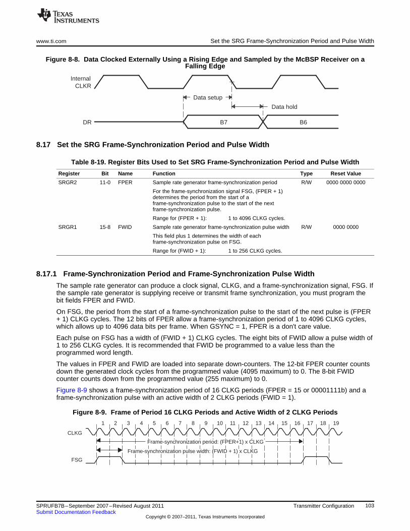
B6B7DR
CLKR
Data holdÁÁÁÁÁÁÁÁData setup
Internal
FSG
CLKG
19181716151413121110987654321
Frame-synchronization period: (FPER+1) x CLKG
Frame-synchronization pulse width: (FWID + 1) x CLKG
www.ti.com Set the SRG Frame-Synchronization Period and Pulse Width
Figure 8-8. Data Clocked Externally Using a Rising Edge and Sampled by the McBSP Receiver on aFalling Edge
8.17 Set the SRG Frame-Synchronization Period and Pulse Width
Table 8-19. Register Bits Used to Set SRG Frame-Synchronization Period and Pulse Width
Register Bit Name Function Type Reset Value
SRGR2 11-0 FPER Sample rate generator frame-synchronization period R/W 0000 0000 0000
For the frame-synchronization signal FSG, (FPER + 1)determines the period from the start of aframe-synchronization pulse to the start of the nextframe-synchronization pulse.
Range for (FPER + 1): 1 to 4096 CLKG cycles.
SRGR1 15-8 FWID Sample rate generator frame-synchronization pulse width R/W 0000 0000
This field plus 1 determines the width of eachframe-synchronization pulse on FSG.
Range for (FWID + 1): 1 to 256 CLKG cycles.
8.17.1 Frame-Synchronization Period and Frame-Synchronization Pulse Width
The sample rate generator can produce a clock signal, CLKG, and a frame-synchronization signal, FSG. Ifthe sample rate generator is supplying receive or transmit frame synchronization, you must program thebit fields FPER and FWID.
On FSG, the period from the start of a frame-synchronization pulse to the start of the next pulse is (FPER+ 1) CLKG cycles. The 12 bits of FPER allow a frame-synchronization period of 1 to 4096 CLKG cycles,which allows up to 4096 data bits per frame. When GSYNC = 1, FPER is a don't care value.
Each pulse on FSG has a width of (FWID + 1) CLKG cycles. The eight bits of FWID allow a pulse width of1 to 256 CLKG cycles. It is recommended that FWID be programmed to a value less than theprogrammed word length.
The values in FPER and FWID are loaded into separate down-counters. The 12-bit FPER counter countsdown the generated clock cycles from the programmed value (4095 maximum) to 0. The 8-bit FWIDcounter counts down from the programmed value (255 maximum) to 0.
Figure 8-9 shows a frame-synchronization period of 16 CLKG periods (FPER = 15 or 00001111b) and aframe-synchronization pulse with an active width of 2 CLKG periods (FWID = 1).
Figure 8-9. Frame of Period 16 CLKG Periods and Active Width of 2 CLKG Periods
103SPRUFB7B–September 2007–Revised August 2011 Transmitter ConfigurationSubmit Documentation Feedback
Copyright © 2007–2011, Texas Instruments Incorporated
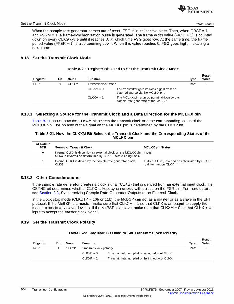
Set the Transmit Clock Mode www.ti.com
When the sample rate generator comes out of reset, FSG is in its inactive state. Then, when GRST = 1and FSGM = 1, a frame-synchronization pulse is generated. The frame width value (FWID + 1) is counteddown on every CLKG cycle until it reaches 0, at which time FSG goes low. At the same time, the frameperiod value (FPER + 1) is also counting down. When this value reaches 0, FSG goes high, indicating anew frame.
8.18 Set the Transmit Clock Mode
Table 8-20. Register Bit Used to Set the Transmit Clock Mode
ResetRegister Bit Name Function Type Value
PCR 9 CLKXM Transmit clock mode R/W 0
CLKXM = 0 The transmitter gets its clock signal from anexternal source via the MCLKX pin.
CLKXM = 1 The MCLKX pin is an output pin driven by thesample rate generator of the McBSP.
8.18.1 Selecting a Source for the Transmit Clock and a Data Direction for the MCLKX pin
Table 8-21 shows how the CLKXM bit selects the transmit clock and the corresponding status of theMCLKX pin. The polarity of the signal on the MCLKX pin is determined by the CLKXP bit.
Table 8-21. How the CLKXM Bit Selects the Transmit Clock and the Corresponding Status of theMCLKX pin
CLKXM inPCR Source of Transmit Clock MCLKX pin Status
0 Internal CLKX is driven by an external clock on the MCLKX pin. InputCLKX is inverted as determined by CLKXP before being used.
1 Internal CLKX is driven by the sample rate generator clock, Output. CLKG, inverted as determined by CLKXP,CLKG. is driven out on CLKX.
8.18.2 Other Considerations
If the sample rate generator creates a clock signal (CLKG) that is derived from an external input clock, theGSYNC bit determines whether CLKG is kept synchronized with pulses on the FSR pin. For more details,see Section 3.3, Synchronizing Sample Rate Generator Outputs to an External Clock.
In the clock stop mode (CLKSTP = 10b or 11b), the McBSP can act as a master or as a slave in the SPIprotocol. If the McBSP is a master, make sure that CLKXM = 1 so that CLKX is an output to supply themaster clock to any slave devices. If the McBSP is a slave, make sure that CLKXM = 0 so that CLKX is aninput to accept the master clock signal.
8.19 Set the Transmit Clock Polarity
Table 8-22. Register Bit Used to Set Transmit Clock Polarity
ResetRegister Bit Name Function Type Value
PCR 1 CLKXP Transmit clock polarity R/W 0
CLKXP = 0 Transmit data sampled on rising edge of CLKX.
CLKXP = 1 Transmit data sampled on falling edge of CLKX.
104 Transmitter Configuration SPRUFB7B–September 2007–Revised August 2011Submit Documentation Feedback
Copyright © 2007–2011, Texas Instruments Incorporated
B6B7DR
CLKR
Data holdÁÁÁÁÁÁÁÁData setup
Internal
www.ti.com Set the Transmit Clock Polarity
8.19.1 Frame Synchronization Pulses, Clock Signals, and Their Polarities
Transmit frame-synchronization pulses can be either generated internally by the sample rate generator(see Section 3.2) or driven by an external source. The source of frame synchronization is selected byprogramming the mode bit, FSXM, in PCR. FSX is also affected by the FSGM bit in SRGR2. Forinformation about the effects of FSXM and FSGM, see Section 8.15, Set the TransmitFrame-Synchronization Mode). Similarly, transmit clocks can be selected to be inputs or outputs byprogramming the mode bit, CLKXM, in the PCR (see Section 8.18, Set the Transmit Clock Mode).
When FSR and FSX are inputs (FSXM = FSRM= 0, external frame-synchronization pulses), the McBSPdetects them on the internal falling edge of clock, internal MCLKR, and internal CLKX, respectively. Thereceive data arriving at the DR pin is also sampled on the falling edge of internal MCLKR. These internalclock signals are either derived from external source via CLK(R/X) pins or driven by the sample rategenerator clock (CLKG) internal to the McBSP.
When FSR and FSX are outputs, implying that they are driven by the sample rate generator, they aregenerated (transition to their active state) on the rising edge of internal clock, CLK(R/X). Similarly, data onthe DX pin is output on the rising edge of internal CLKX.
FSRP, FSXP, CLKRP, and CLKXP in the pin control register (PCR) configure the polarities of the FSR,FSX, MCLKR, and CLKX signals, respectively. All frame-synchronization signals (internal FSR, internalFSX) that are internal to the serial port are active high. If the serial port is configured for external framesynchronization (FSR/FSX are inputs to McBSP), and FSRP = FSXP = 1, the external active-lowframe-synchronization signals are inverted before being sent to the receiver (internal FSR) and transmitter(internal FSX). Similarly, if internal synchronization (FSR/FSX are output pins and GSYNC = 0) isselected, the internal active-high frame-synchronization signals are inverted, if the polarity bit FS(R/X)P =1, before being sent to the FS(R/X) pin.
On the transmit side, the transmit clock polarity bit, CLKXP, sets the edge used to shift and clock outtransmit data. Data is always transmitted on the rising edge of internal CLKX. If CLKXP = 1 and externalclocking is selected (CLKXM = 0 and CLKX is an input), the external falling-edge triggered input clock onCLKX is inverted to a rising-edge triggered clock before being sent to the transmitter. If CLKXP = 1 andinternal clocking is selected (CLKXM = 1 and CLKX is an output pin), the internal (rising-edge triggered)clock, internal CLKX, is inverted before being sent out on the MCLKX pin.
Similarly, the receiver can reliably sample data that is clocked with a rising edge clock (by the transmitter).The receive clock polarity bit, CLKRP, sets the edge used to sample received data. The receive data isalways sampled on the falling edge of internal MCLKR. Therefore, if CLKRP = 1 and external clocking isselected (CLKRM = 0 and CLKR is an input pin), the external rising-edge triggered input clock on CLKR isinverted to a falling-edge triggered clock before being sent to the receiver. If CLKRP = 1 and internalclocking is selected (CLKRM = 1), the internal falling-edge triggered clock is inverted to a rising-edgetriggered clock before being sent out on the MCLKR pin.
CLKRP = CLKXP in a system where the same clock (internal or external) is used to clock the receiver andtransmitter. The receiver uses the opposite edge as the transmitter to ensure valid setup and hold of dataaround this edge (see Figure 8-8).
Figure 8-10 shows how data clocked by an external serial device using a rising edge can be sampled bythe McBSP receiver on the falling edge of the same clock.
Figure 8-10. Data Clocked Externally Using a Rising Edge and Sampled by the McBSP Receiver on aFalling Edge
105SPRUFB7B–September 2007–Revised August 2011 Transmitter ConfigurationSubmit Documentation Feedback
Copyright © 2007–2011, Texas Instruments Incorporated

106 Transmitter Configuration SPRUFB7B–September 2007–Revised August 2011Submit Documentation Feedback
Copyright © 2007–2011, Texas Instruments Incorporated
Chapter 9SPRUFB7B–September 2007–Revised August 2011
Emulation and Reset Considerations
This section covers the following topics:
• How to program McBSP response to a breakpoint in the high-level language debugger (seeSection 9.1)
• How to reset and initialize the various parts of the McBSP (see Section 9.2)
Topic ........................................................................................................................... Page
9.1 McBSP Emulation Mode ................................................................................... 1089.2 Resetting and Initializing McBSPs ..................................................................... 108
107SPRUFB7B–September 2007–Revised August 2011 Emulation and Reset ConsiderationsSubmit Documentation Feedback
Copyright © 2007–2011, Texas Instruments Incorporated
McBSP Emulation Mode www.ti.com
9.1 McBSP Emulation Mode
FREE and SOFT are special emulation bits in SPCR2 that determine the state of the McBSP when abreakpoint is encountered in the high-level language debugger. If FREE = 1, the clock continues to runupon a software breakpoint and data is still shifted out. When FREE = 1, the SOFT bit is a don't care.
If FREE = 0, the SOFT bit takes effect. If SOFT = 0 when breakpoint occurs, the clock stops immediately,aborting a transmission. If SOFT = 1 and a breakpoint occurs while transmission is in progress, thetransmission continues until completion of the transfer and then the clock halts. These options are listed inTable 9-1.
The McBSP receiver functions in a similar fashion. If a mode other than the immediate stop mode (SOFT= FREE = 0) is chosen, the receiver continues running and an overrun error is possible.
Table 9-1. McBSP Emulation Modes Selectable with FREE and SOFT Bits of SPCR2
FREE SOFT McBSP Emulation Mode
0 0 Immediate stop mode (reset condition)
The transmitter or receiver stops immediately in response to a breakpoint.
0 1 Soft stop mode
When a breakpoint occurs, the transmitter stops after completion of the current word. The receiver isnot affected.
1 0 or 1 Free run mode
The transmitter and receiver continue to run when a breakpoint occurs.
9.2 Resetting and Initializing McBSPs
9.2.1 McBSP Pin States: DSP Reset Versus Receiver/Transmitter Reset
Table 9-2 shows the state of McBSP pins when the serial port is reset due to direct receiver or transmitterreset on the 2833x device.
Table 9-2. Reset State of Each McBSP Pin
State Forced by Device State Forced byPin Possible State(s) (1) Reset Receiver/Transmitter Reset
Receiver reset (RRST = 0 and GRST = 1)
MDRx I GPIO-input Input
MCLKRx I/O/Z GPIO-input Known state if input; MCLKR running if output
MFSRx I/O/Z GPIO-input Known state if input; FSRP inactive state if output
Transmitter reset (XRST = 0 and GRST = 1)
MDXx O/Z GPIO Input High impedance
MCLKXx I/O/Z GPIO-input Known state if input; CLKX running if output
MFSXx I/O/Z GPIO-input Known state if input; FSXP inactive state if output(1) In Possible State(s) column, I = Input, O = Output, Z = High impedance. In the 28x family, at device reset, all I/Os default to
GPIO function and generally as inputs.
9.2.2 Device Reset, McBSP Reset, and Sample Rate Generator Reset
When the McBSP is reset in either of the above two ways, the machine is reset to its initial state, includingreset of all counters and status bits. The receive status bits include RFULL, RRDY, and RSYNCERR. Thetransmit status bits include XEMPTY, XRDY, and XSYNCERR.
• Device reset. When the whole DSP is reset (XRS signal is driven low), all McBSP pins are in GPIOmode. When the device is pulled out of reset, the clock to the McBSP modules remains disabled.
108 Emulation and Reset Considerations SPRUFB7B–September 2007–Revised August 2011Submit Documentation Feedback
Copyright © 2007–2011, Texas Instruments Incorporated
www.ti.com Resetting and Initializing McBSPs
• McBSP reset. When the receiver and transmitter reset bits, RRST and XRST, are loaded with 0s, therespective portions of the McBSP are reset and activity in the corresponding section of the serial portstops. Input-only pins such as MDRx, and all other pins that are configured as inputs are in a knownstate. The MFSRx and MFSXx pins are driven to their inactive state if they are not outputs. If theMCLKR and MCLKX pins are programmed as outputs, they are driven by CLKG, provided that GRST= 1. Lastly, the MDXx pin is in the high-impedance state when the transmitter and/or the device isreset.
During normal operation, the sample rate generator is reset if the GRST bit is cleared. GRST must be0 only when neither the transmitter nor the receiver is using the sample rate generator. In this case,the internal sample rate generator clock (CLKG) and its frame-synchronization signal (FSG) are driveninactive low.
When the sample rate generator is not in the reset state (GRST = 1), pins MFSRx and MFSXx are inan inactive state when RRST = 0 and XRST = 0, respectively, even if they are outputs driven by FSG.This ensures that when only one portion of the McBSP is in reset, the other portion can continueoperation when GRST = 1 and its frame synchronization is driven by FSG.
• Sample rate generator reset. The sample rate generator is reset when GRST is loaded with 0.
When neither the transmitter nor the receiver is fed by CLKG and FSG, you can reset the sample rategenerator by clearing GRST. In this case, CLKG and FSG are driven inactive low. If you then setGRST, CLKG starts and runs as programmed. Later, if GRST = 1, FSG pulses active high after theprogrammed number of CLKG cycles has elapsed.
9.2.3 McBSP Initialization Procedure
The serial port initialization procedure is as follows:
1. Make XRST = RRST = GRST = 0 in SPCR[1,2]. If coming out of a device reset, this step is notrequired.
2. While the serial port is in the reset state, program only the McBSP configuration registers (not the dataregisters) as required.
3. Wait for two clock cycles. This ensures proper internal synchronization.
4. Set up data acquisition as required (such as writing to DXR[1,2]).
5. Make XRST = RRST = 1 to enable the serial port. Make sure that as you set these reset bits, you donot modify any of the other bits in SPCR1 and SPCR2. Otherwise, you change the configuration youselected in step 2.
6. Set FRST = 1, if internally generated frame synchronization is required.
7. Wait two clock cycles for the receiver and transmitter to become active.
Alternatively, on either write (step 1 or 5), the transmitter and receiver can be placed in or taken out ofreset individually by modifying the desired bit.
The above procedure for reset/initialization can be applied in general when the receiver or transmittermust be reset during its normal operation and when the sample rate generator is not used for eitheroperation.
NOTE:1. The necessary duration of the active-low period of XRST or RRST is at least two
MCLKR/CLKX cycles.2. The appropriate bits in serial port configuration registers SPCR[1,2], PCR, RCR[1,2],
XCR[1,2], and SRGR[1,2] must only be modified when the affected portion of the serialport is in its reset state.
3. In most cases, the data transmit registers (DXR[1,2]) must be loaded by the CPU or bythe DMA controller only when the transmitter is enabled (XRST = 1). An exception tothis rule is when these registers are used for companding internal data (seeSection 2.2.2, Capability to Compand Internal Data).
4. The bits of the channel control registers—MCR[1,2], RCER[A-H], XCER[A-H]—can bemodified at any time as long as they are not being used by the currentreception/transmission in a multichannel selection mode.
109SPRUFB7B–September 2007–Revised August 2011 Emulation and Reset ConsiderationsSubmit Documentation Feedback
Copyright © 2007–2011, Texas Instruments Incorporated
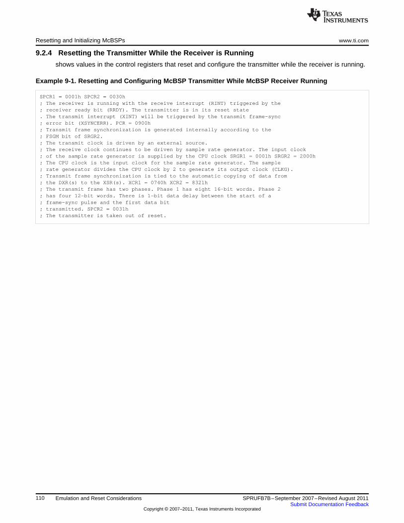
Resetting and Initializing McBSPs www.ti.com
9.2.4 Resetting the Transmitter While the Receiver is Running
shows values in the control registers that reset and configure the transmitter while the receiver is running.
Example 9-1. Resetting and Configuring McBSP Transmitter While McBSP Receiver Running
SPCR1 = 0001h SPCR2 = 0030h; The receiver is running with the receive interrupt (RINT) triggered by the; receiver ready bit (RRDY). The transmitter is in its reset state. The transmit interrupt (XINT) will be triggered by the transmit frame-sync; error bit (XSYNCERR). PCR = 0900h; Transmit frame synchronization is generated internally according to the; FSGM bit of SRGR2.; The transmit clock is driven by an external source.; The receive clock continues to be driven by sample rate generator. The input clock; of the sample rate generator is supplied by the CPU clock SRGR1 = 0001h SRGR2 = 2000h; The CPU clock is the input clock for the sample rate generator. The sample; rate generator divides the CPU clock by 2 to generate its output clock (CLKG).; Transmit frame synchronization is tied to the automatic copying of data from; the DXR(s) to the XSR(s). XCR1 = 0740h XCR2 = 8321h; The transmit frame has two phases. Phase 1 has eight 16-bit words. Phase 2; has four 12-bit words. There is 1-bit data delay between the start of a; frame-sync pulse and the first data bit; transmitted. SPCR2 = 0031h; The transmitter is taken out of reset.
110 Emulation and Reset Considerations SPRUFB7B–September 2007–Revised August 2011Submit Documentation Feedback
Copyright © 2007–2011, Texas Instruments Incorporated
Chapter 10SPRUFB7B–September 2007–Revised August 2011
Data Packing Examples
This section shows two ways to implement data packing in the McBSP.
Topic ........................................................................................................................... Page
10.1 Data Packing Using Frame Length and Word Length ........................................... 11210.2 Data Packing Using Word Length and the Frame-Synchronization Ignore
Function ......................................................................................................... 113
111SPRUFB7B–September 2007–Revised August 2011 Data Packing ExamplesSubmit Documentation Feedback
Copyright © 2007–2011, Texas Instruments Incorporated
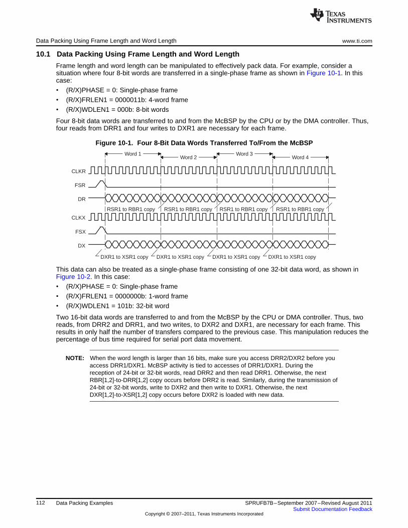
DX
FSX
CLKX
DR
FSR
CLKR
DXR1 to XSR1 copyDXR1 to XSR1 copyDXR1 to XSR1 copyDXR1 to XSR1 copy
ÁÁÁÁÁÁÁÁ ÁÁÁÁÁÁÁÁÁÁÁÁÁÁÁÁÁÁÁÁÁÁÁÁÁÁÁÁÁÁÁÁÁÁÁÁÁÁÁÁÁÁÁÁÁ ÁÁÁÁÁÁÁÁÁÁÁÁÁÁÁÁÁÁÁÁÁÁÁÁÁÁÁÁÁÁÁÁÁÁÁÁÁÁÁÁÁÁÁÁÁÁÁÁÁÁÁÁÁÁÁÁÁÁÁÁÁÁÁÁÁÁÁÁÁÁÁÁÁÁÁÁÁÁÁÁÁÁÁÁ ÁÁÁÁÁÁÁÁÁÁÁÁÁÁÁÁÁÁÁÁÁÁÁÁÁÁÁÁÁÁÁÁÁÁÁÁ ÁÁÁÁÁÁ ÁÁÁÁÁÁ RSR1 to RBR1 copyRSR1 to RBR1 copyRSR1 to RBR1 copyRSR1 to RBR1 copy
ÁÁÁÁÁÁ ÁÁÁÁÁÁÁÁÁÁÁÁÁÁÁÁÁÁÁÁÁÁÁÁÁÁÁÁÁÁÁÁÁÁÁÁÁÁÁÁÁÁÁÁÁÁÁÁÁÁÁÁÁÁÁÁÁÁÁÁÁÁÁÁÁÁÁÁÁÁÁÁ ÁÁÁÁÁÁÁÁÁÁÁÁÁÁÁÁÁÁÁÁÁÁÁÁÁÁÁÁÁÁÁÁÁÁÁÁ ÁÁÁÁÁÁÁÁÁÁÁÁÁÁÁÁÁÁÁÁÁÁÁÁÁÁÁÁÁÁÁÁÁÁÁÁÁÁÁÁÁÁÁÁÁÁÁÁÁÁÁÁ ÁÁÁÁÁÁÁÁÁÁÁÁÁÁÁÁÁÁÁÁÁÁÁÁÁÁÁÁÁÁÁÁÁÁÁÁÁÁÁÁÁÁÁÁÁÁÁÁÁÁÁÁÁÁÁÁÁÁÁÁÁÁÁÁÁÁÁÁÁÁÁÁÁÁÁÁ Word 4Word 3
Word 2Word 1
Data Packing Using Frame Length and Word Length www.ti.com
10.1 Data Packing Using Frame Length and Word Length
Frame length and word length can be manipulated to effectively pack data. For example, consider asituation where four 8-bit words are transferred in a single-phase frame as shown in Figure 10-1. In thiscase:
• (R/X)PHASE = 0: Single-phase frame
• (R/X)FRLEN1 = 0000011b: 4-word frame
• (R/X)WDLEN1 = 000b: 8-bit words
Four 8-bit data words are transferred to and from the McBSP by the CPU or by the DMA controller. Thus,four reads from DRR1 and four writes to DXR1 are necessary for each frame.
Figure 10-1. Four 8-Bit Data Words Transferred To/From the McBSP
This data can also be treated as a single-phase frame consisting of one 32-bit data word, as shown inFigure 10-2. In this case:
• (R/X)PHASE = 0: Single-phase frame
• (R/X)FRLEN1 = 0000000b: 1-word frame
• (R/X)WDLEN1 = 101b: 32-bit word
Two 16-bit data words are transferred to and from the McBSP by the CPU or DMA controller. Thus, tworeads, from DRR2 and DRR1, and two writes, to DXR2 and DXR1, are necessary for each frame. Thisresults in only half the number of transfers compared to the previous case. This manipulation reduces thepercentage of bus time required for serial port data movement.
NOTE: When the word length is larger than 16 bits, make sure you access DRR2/DXR2 before youaccess DRR1/DXR1. McBSP activity is tied to accesses of DRR1/DXR1. During thereception of 24-bit or 32-bit words, read DRR2 and then read DRR1. Otherwise, the nextRBR[1,2]-to-DRR[1,2] copy occurs before DRR2 is read. Similarly, during the transmission of24-bit or 32-bit words, write to DXR2 and then write to DXR1. Otherwise, the nextDXR[1,2]-to-XSR[1,2] copy occurs before DXR2 is loaded with new data.
112 Data Packing Examples SPRUFB7B–September 2007–Revised August 2011Submit Documentation Feedback
Copyright © 2007–2011, Texas Instruments Incorporated
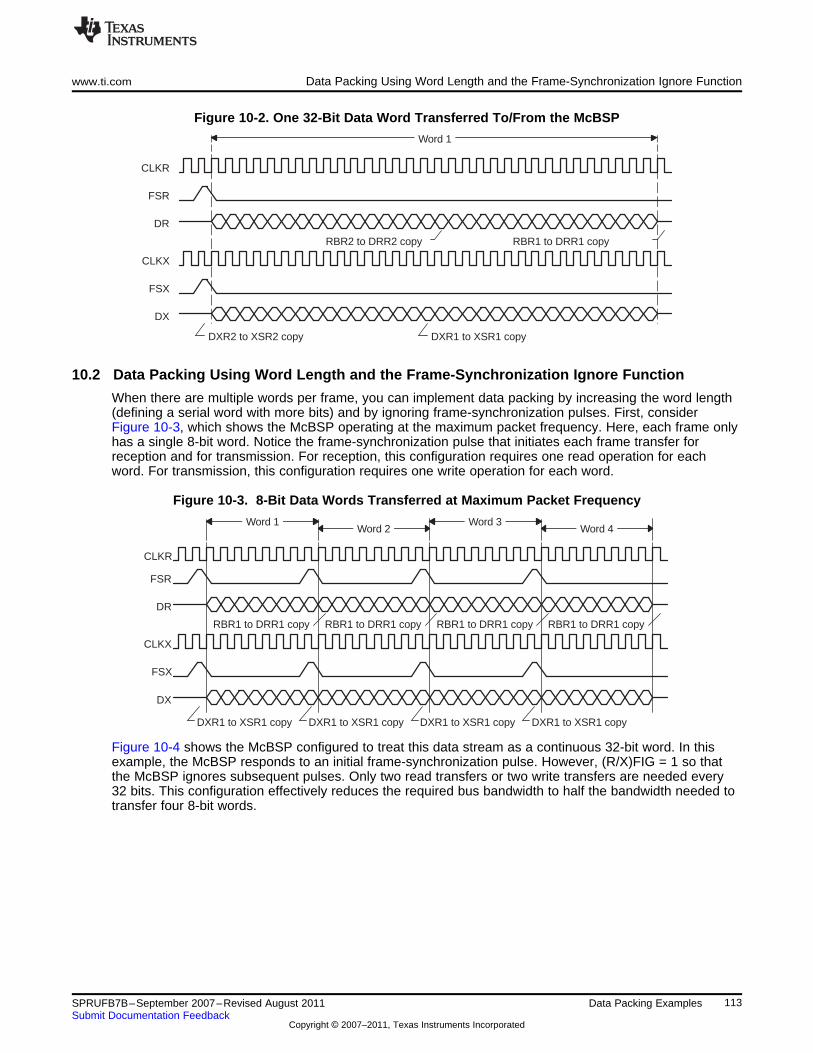
DXR1 to XSR1 copyDXR2 to XSR2 copy
RBR1 to DRR1 copyRBR2 to DRR2 copy
DX
FSX
CLKX
DR
FSR
CLKR ÁÁÁÁÁÁÁÁÁ ÁÁÁÁÁÁÁÁÁÁÁÁÁÁÁÁÁÁÁÁÁÁÁÁÁÁÁÁÁÁÁÁÁÁÁÁÁÁÁÁÁÁÁÁÁÁÁÁÁÁÁÁÁÁÁÁÁÁÁÁ ÁÁÁÁÁÁÁÁÁÁÁÁÁÁÁÁÁÁÁÁÁÁÁÁÁÁÁÁÁÁÁÁÁÁÁÁÁÁÁÁÁÁÁÁÁÁÁÁÁÁÁÁÁÁÁÁÁÁÁÁÁÁÁÁÁÁÁÁÁÁÁÁÁÁÁÁÁÁÁÁÁÁÁÁÁÁÁÁÁÁÁÁÁÁÁÁÁÁÁÁÁÁÁÁÁÁÁÁÁÁÁÁÁÁÁÁ ÁÁÁÁÁÁÁÁÁÁÁÁÁÁÁÁÁÁÁÁÁÁÁÁÁÁÁÁÁÁÁÁÁÁÁÁÁÁÁÁÁÁÁÁ ÁÁÁÁÁÁÁÁ ÁÁÁÁ ÁÁÁÁÁÁÁÁÁÁÁÁ ÁÁÁÁÁÁÁÁÁÁÁÁÁÁÁÁÁÁÁÁÁÁÁÁÁÁÁÁÁÁÁÁÁÁÁÁÁÁÁÁÁÁÁÁÁÁÁÁÁÁÁÁÁÁÁÁÁÁÁÁÁÁÁÁÁÁÁÁÁÁÁÁ ÁÁÁÁÁÁÁÁÁÁÁÁÁÁÁÁÁÁÁÁÁÁÁÁÁÁÁÁÁÁÁÁ ÁÁÁÁÁÁÁÁÁÁÁÁÁÁÁÁÁÁÁÁÁÁÁÁÁÁÁÁÁÁÁÁÁÁÁÁÁÁÁÁÁÁÁÁÁÁÁÁÁÁÁÁÁÁÁÁ ÁÁÁÁÁÁÁÁÁÁÁÁÁÁÁÁÁÁÁÁÁÁÁÁÁÁÁÁÁÁÁÁÁÁÁÁÁÁÁÁÁÁÁÁÁÁÁÁÁÁÁÁÁÁÁÁÁÁÁÁÁÁÁÁÁÁÁÁÁÁÁÁ Word 1
DX
FSX
CLKX
DR
FSR
CLKR
DXR1 to XSR1 copyDXR1 to XSR1 copyDXR1 to XSR1 copyDXR1 to XSR1 copy
ÁÁÁÁÁÁÁÁ ÁÁÁÁÁÁÁÁÁÁÁÁÁÁÁÁÁÁÁÁÁÁÁÁÁÁÁÁÁÁÁÁÁÁÁÁÁÁÁÁÁÁÁÁÁÁÁÁÁÁÁÁÁÁÁÁÁÁÁÁ ÁÁÁÁÁÁÁÁÁÁÁÁÁÁÁÁÁÁÁÁÁÁÁÁÁÁÁÁÁÁÁÁÁÁÁÁÁÁÁÁÁÁÁÁÁÁÁÁÁÁÁÁÁÁÁÁÁÁÁÁÁÁÁÁÁÁÁÁÁÁÁÁÁÁÁÁÁÁÁÁÁÁÁÁÁÁÁÁÁÁÁÁÁÁÁÁÁÁÁÁÁÁÁÁÁÁÁÁ ÁÁÁÁÁÁÁÁÁÁÁÁÁÁÁÁÁÁÁÁÁÁÁÁÁÁÁÁÁÁÁÁÁÁÁÁÁÁÁÁÁÁÁÁÁÁÁÁ ÁÁÁÁÁÁÁÁ ÁÁÁÁÁÁÁÁ RBR1 to DRR1 copyRBR1 to DRR1 copyRBR1 to DRR1 copyRBR1 to DRR1 copy
ÁÁÁÁÁÁ ÁÁÁÁÁÁÁÁÁÁÁÁÁÁÁÁÁÁÁÁÁÁÁÁÁÁÁÁÁÁÁÁÁÁÁÁÁÁÁÁÁÁÁÁÁÁÁÁÁÁÁÁÁÁÁÁÁÁÁÁÁÁÁÁÁÁÁÁÁÁÁÁ ÁÁÁÁÁÁÁÁÁÁÁÁÁÁÁÁÁÁÁÁÁÁÁÁÁÁÁÁÁÁÁÁ ÁÁÁÁÁÁÁÁÁÁÁÁÁÁÁÁÁÁÁÁÁÁÁÁÁÁÁÁÁÁÁÁÁÁÁÁÁÁÁÁÁÁÁÁÁÁÁÁÁÁÁÁ ÁÁÁÁÁÁÁÁÁÁÁÁÁÁÁÁÁÁÁÁÁÁÁÁÁÁÁÁÁÁÁÁÁÁÁÁÁÁÁÁÁÁÁÁÁÁÁÁÁÁÁÁÁÁÁÁÁÁÁÁÁÁÁÁÁÁÁÁÁÁÁÁÁÁÁÁ Word 4Word 3
Word 2Word 1
www.ti.com Data Packing Using Word Length and the Frame-Synchronization Ignore Function
Figure 10-2. One 32-Bit Data Word Transferred To/From the McBSP
10.2 Data Packing Using Word Length and the Frame-Synchronization Ignore Function
When there are multiple words per frame, you can implement data packing by increasing the word length(defining a serial word with more bits) and by ignoring frame-synchronization pulses. First, considerFigure 10-3, which shows the McBSP operating at the maximum packet frequency. Here, each frame onlyhas a single 8-bit word. Notice the frame-synchronization pulse that initiates each frame transfer forreception and for transmission. For reception, this configuration requires one read operation for eachword. For transmission, this configuration requires one write operation for each word.
Figure 10-3. 8-Bit Data Words Transferred at Maximum Packet Frequency
Figure 10-4 shows the McBSP configured to treat this data stream as a continuous 32-bit word. In thisexample, the McBSP responds to an initial frame-synchronization pulse. However, (R/X)FIG = 1 so thatthe McBSP ignores subsequent pulses. Only two read transfers or two write transfers are needed every32 bits. This configuration effectively reduces the required bus bandwidth to half the bandwidth needed totransfer four 8-bit words.
113SPRUFB7B–September 2007–Revised August 2011 Data Packing ExamplesSubmit Documentation Feedback
Copyright © 2007–2011, Texas Instruments Incorporated
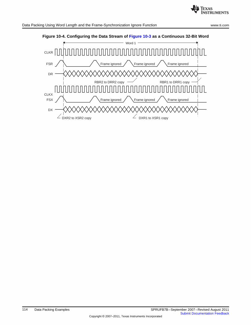
Word 1
DXR2 to XSR2 copy
ÁÁÁÁÁÁÁÁÁÁÁÁÁÁÁÁÁÁÁÁÁÁÁÁÁÁÁÁÁÁÁÁÁÁÁÁÁÁÁÁÁÁÁÁÁÁÁÁÁÁÁÁÁÁÁÁÁÁÁÁÁÁÁÁÁÁÁÁÁÁÁÁÁÁÁÁÁÁÁÁÁÁÁÁÁÁÁÁÁÁÁÁÁÁÁÁÁÁÁÁÁÁÁÁÁÁÁÁÁÁÁÁÁÁÁÁÁÁÁÁÁÁÁÁÁÁÁÁ ÁÁÁÁ ÁÁÁÁÁÁÁÁÁÁÁÁÁÁÁÁÁÁÁÁÁÁÁÁÁÁÁÁÁÁÁÁÁÁÁÁÁÁÁÁÁÁÁÁÁÁÁÁÁÁÁÁÁÁÁÁÁÁÁÁÁÁÁÁÁÁÁÁÁÁÁÁÁÁÁÁÁÁÁÁ ÁÁÁÁÁÁÁÁÁÁÁÁCLKX
ÁÁÁÁÁÁÁÁ ÁÁÁÁÁÁÁÁÁÁÁÁFrame ignored Frame ignored
ÁÁÁÁFSX
DX
Frame ignored
DXR1 to XSR1 copy
DR
FSR
CLKR
RBR1 to DRR1 copy RBR2 to DRR2 copy
Frame ignoredFrame ignoredFrame ignored
ÁÁÁÁÁÁÁÁ ÁÁÁÁÁÁÁÁÁÁÁÁÁÁÁÁÁÁÁÁÁÁÁÁÁÁÁÁÁÁÁÁÁÁÁÁÁÁÁÁÁÁÁÁÁÁÁÁÁÁÁÁÁÁÁÁÁÁÁÁÁÁÁÁÁÁÁÁÁÁÁÁÁÁÁÁÁÁÁÁÁÁÁÁÁÁÁÁÁÁÁÁÁÁÁÁÁÁÁÁÁÁÁÁÁÁÁÁÁÁÁÁ ÁÁÁÁÁÁÁÁÁÁÁÁÁÁÁÁÁÁÁÁ ÁÁÁÁÁÁÁÁÁÁÁÁÁÁÁÁÁÁÁÁÁÁÁÁÁÁÁÁÁÁÁÁÁÁÁÁÁÁÁÁÁÁÁÁÁÁÁÁÁÁÁÁÁÁÁÁÁÁÁÁÁÁÁÁÁÁÁÁÁÁÁÁÁÁÁÁÁÁÁÁÁÁÁÁÁÁÁÁÁÁÁÁÁÁÁÁÁÁÁÁÁÁÁÁÁÁÁÁData Packing Using Word Length and the Frame-Synchronization Ignore Function www.ti.com
Figure 10-4. Configuring the Data Stream of Figure 10-3 as a Continuous 32-Bit Word
114 Data Packing Examples SPRUFB7B–September 2007–Revised August 2011Submit Documentation Feedback
Copyright © 2007–2011, Texas Instruments Incorporated
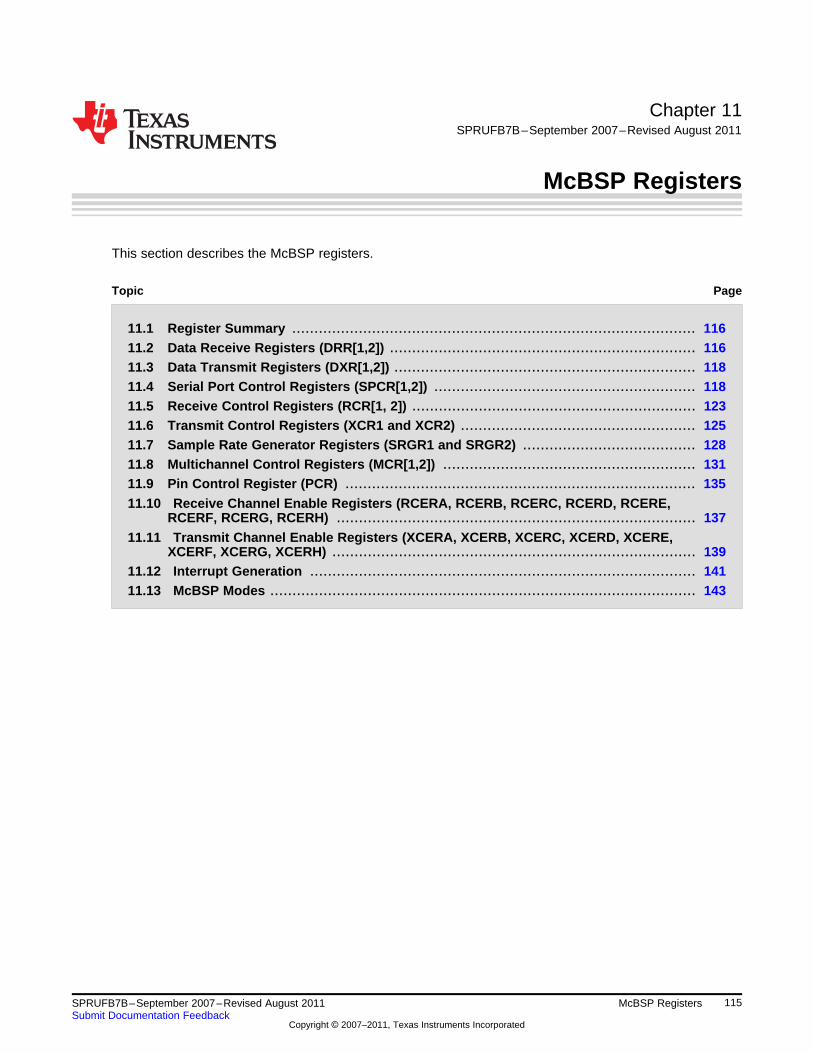
Chapter 11SPRUFB7B–September 2007–Revised August 2011
McBSP Registers
This section describes the McBSP registers.
Topic ........................................................................................................................... Page
11.1 Register Summary ........................................................................................... 11611.2 Data Receive Registers (DRR[1,2]) ..................................................................... 11611.3 Data Transmit Registers (DXR[1,2]) .................................................................... 11811.4 Serial Port Control Registers (SPCR[1,2]) ........................................................... 11811.5 Receive Control Registers (RCR[1, 2]) ................................................................ 12311.6 Transmit Control Registers (XCR1 and XCR2) ..................................................... 12511.7 Sample Rate Generator Registers (SRGR1 and SRGR2) ....................................... 12811.8 Multichannel Control Registers (MCR[1,2]) ......................................................... 13111.9 Pin Control Register (PCR) ............................................................................... 13511.10 Receive Channel Enable Registers (RCERA, RCERB, RCERC, RCERD, RCERE,
RCERF, RCERG, RCERH) ................................................................................. 13711.11 Transmit Channel Enable Registers (XCERA, XCERB, XCERC, XCERD, XCERE,
XCERF, XCERG, XCERH) .................................................................................. 13911.12 Interrupt Generation ....................................................................................... 14111.13 McBSP Modes ................................................................................................ 143
115SPRUFB7B–September 2007–Revised August 2011 McBSP RegistersSubmit Documentation Feedback
Copyright © 2007–2011, Texas Instruments Incorporated
Register Summary www.ti.com
11.1 Register Summary
Table 11-1 shows the registers accessible on each McBSP. Section 11.2 through Section 11.11 describethe register bits.
Table 11-1. McBSP Register Summary
Name McBSP-A McBSP-B Type Reset Value DescriptionAddress Address
Data Registers, Receive, Transmit
DRR2 0x5000 0x5040 R 0x0000 McBSP Data Receive Register 2
DRR1 0x5001 0x5041 R 0x0000 McBSP Data Receive Register 1
DXR2 0x5002 0x5042 W 0x0000 McBSP Data Transmit Register 2
DXR1 0x5003 0x5043 W 0x0000 McBSP Data Transmit Register 1
McBSP Control Registers
SPCR2 0x5004 0x5044 R/W 0x0000 McBSP Serial Port Control Register 2
SPCR1 0x5005 0x5045 R/W 0x0000 McBSP Serial Port Control Register 1
RCR2 0x5006 0x5046 R/W 0x0000 McBSP Receive Control Register 2
RCR1 0x5007 0x5047 R/W 0x0000 McBSP Receive Control Register 1
XCR2 0x5008 0x5048 R/W 0x0000 McBSP Transmit Control Register 2
XCR1 0x5009 0x5049 R/W 0x0000 McBSP Transmit Control Register 1
SRGR2 0x500A 0x504A R/W 0x0000 McBSP Sample Rate Generator Register 2
SRGR1 0x500B 0x504B R/W 0x0000 McBSP Sample Rate Generator Register 1
Multichannel Control Registers
MCR2 0x500C 0x504C R/W 0x0000 McBSP Multichannel Register 2
MCR1 0x500D 0x504D R/W 0x0000 McBSP Multichannel Register 1
RCERA 0x500E 0x504E R/W 0x0000 McBSP Receive Channel Enable Register Partition A
RCERB 0x500F 0x504F R/W 0x0000 McBSP Receive Channel Enable Register Partition B
XCERA 0x5010 0x5050 R/W 0x0000 McBSP Transmit Channel Enable Register Partition A
XCERB 0x5011 0x5051 R/W 0x0000 McBSP Transmit Channel Enable Register Partition B
PCR 0x5012 0x5052 R/W 0x0000 McBSP Pin Control Register
RCERC 0x5013 0x5053 R/W 0x0000 McBSP Receive Channel Enable Register Partition C
RCERD 0x5014 0x5054 R/W 0x0000 McBSP Receive Channel Enable Register Partition D
XCERC 0x5015 0x5055 R/W 0x0000 McBSP Transmit Channel Enable Register Partition C
XCERD 0x5016 0x5056 R/W 0x0000 McBSP Transmit Channel Enable Register Partition D
RCERE 0x5017 0x5057 R/W 0x0000 McBSP Receive Channel Enable Register Partition E
RCERF 0x5018 0x5058 R/W 0x0000 McBSP Receive Channel Enable Register Partition F
XCERE 0x5019 0x5059 R/W 0x0000 McBSP Transmit Channel Enable Register Partition E
XCERF 0x501A 0x505A R/W 0x0000 McBSP Transmit Channel Enable Register Partition F
RCERG 0x501B 0x505B R/W 0x0000 McBSP Receive Channel Enable Register Partition G
RCERH 0x501C 0x505C R/W 0x0000 McBSP Receive Channel Enable Register Partition H
XCERG 0x501D 0x505D R/W 0x0000 McBSP Transmit Channel Enable Register Partition G
XCERH 0x501E 0x505E R/W 0x0000 McBSP Transmit Channel Enable Register Partition H
MFFINT 0x5023 0x5063 R/W 0x0000 McBSP Interrupt Enable Register
11.2 Data Receive Registers (DRR[1,2])
The CPU or the DMA controller reads received data from one or both of the data receive registers (seeFigure 11-1). If the serial word length is 16 bits or smaller, only DRR1 is used. If the serial length is largerthan 16 bits, both DRR1 and DRR2 are used and DRR2 holds the most significant bits. Each frame ofreceive data in the McBSP can have one phase or two phases, each with its own serial word length.
116 McBSP Registers SPRUFB7B–September 2007–Revised August 2011Submit Documentation Feedback
Copyright © 2007–2011, Texas Instruments Incorporated
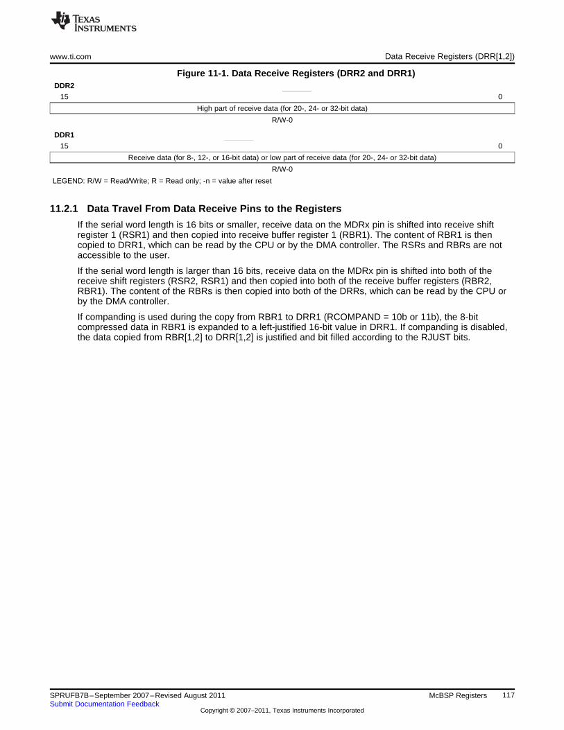
www.ti.com Data Receive Registers (DRR[1,2])
Figure 11-1. Data Receive Registers (DRR2 and DRR1)DDR2
15 0
High part of receive data (for 20-, 24- or 32-bit data)
R/W-0
DDR1
15 0
Receive data (for 8-, 12-, or 16-bit data) or low part of receive data (for 20-, 24- or 32-bit data)
R/W-0
LEGEND: R/W = Read/Write; R = Read only; -n = value after reset
11.2.1 Data Travel From Data Receive Pins to the Registers
If the serial word length is 16 bits or smaller, receive data on the MDRx pin is shifted into receive shiftregister 1 (RSR1) and then copied into receive buffer register 1 (RBR1). The content of RBR1 is thencopied to DRR1, which can be read by the CPU or by the DMA controller. The RSRs and RBRs are notaccessible to the user.
If the serial word length is larger than 16 bits, receive data on the MDRx pin is shifted into both of thereceive shift registers (RSR2, RSR1) and then copied into both of the receive buffer registers (RBR2,RBR1). The content of the RBRs is then copied into both of the DRRs, which can be read by the CPU orby the DMA controller.
If companding is used during the copy from RBR1 to DRR1 (RCOMPAND = 10b or 11b), the 8-bitcompressed data in RBR1 is expanded to a left-justified 16-bit value in DRR1. If companding is disabled,the data copied from RBR[1,2] to DRR[1,2] is justified and bit filled according to the RJUST bits.
117SPRUFB7B–September 2007–Revised August 2011 McBSP RegistersSubmit Documentation Feedback
Copyright © 2007–2011, Texas Instruments Incorporated
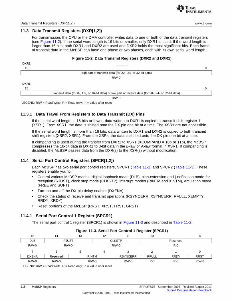
Data Transmit Registers (DXR[1,2]) www.ti.com
11.3 Data Transmit Registers (DXR[1,2])
For transmission, the CPU or the DMA controller writes data to one or both of the data transmit registers(see Figure 11-2). If the serial word length is 16 bits or smaller, only DXR1 is used. If the word length islarger than 16 bits, both DXR1 and DXR2 are used and DXR2 holds the most significant bits. Each frameof transmit data in the McBSP can have one phase or two phases, each with its own serial word length.
Figure 11-2. Data Transmit Registers (DXR2 and DXR1)DXR2
15 0
High part of transmit data (for 20-, 24- or 32-bit data)
R/W-0
DXR1
15 0
Transmit data (for 8-, 12-, or 16-bit data) or low part of receive data (for 20-, 24- or 32-bit data)
R/W-0
LEGEND: R/W = Read/Write; R = Read only; -n = value after reset
11.3.1 Data Travel From Registers to Data Transmit (DX) Pins
If the serial word length is 16 bits or fewer, data written to DXR1 is copied to transmit shift register 1(XSR1). From XSR1, the data is shifted onto the DX pin one bit at a time. The XSRs are not accessible.
If the serial word length is more than 16 bits, data written to DXR1 and DXR2 is copied to both transmitshift registers (XSR2, XSR1). From the XSRs, the data is shifted onto the DX pin one bit at a time.
If companding is used during the transfer from DXR1 to XSR1 (XCOMPAND = 10b or 11b), the McBSPcompresses the 16-bit data in DXR1 to 8-bit data in the μ-law or A-law format in XSR1. If companding isdisabled, the McBSP passes data from the DXR(s) to the XSR(s) without modification.
11.4 Serial Port Control Registers (SPCR[1,2])
Each McBSP has two serial port control registers, SPCR1 (Table 11-2) and SPCR2 (Table 11-3). Theseregisters enable you to:
• Control various McBSP modes: digital loopback mode (DLB), sign-extension and justification mode forreception (RJUST), clock stop mode (CLKSTP), interrupt modes (RINTM and XINTM), emulation mode(FREE and SOFT)
• Turn on and off the DX-pin delay enabler (DXENA)
• Check the status of receive and transmit operations (RSYNCERR, XSYNCERR, RFULL, XEMPTY,RRDY, XRDY)
• Reset portions of the McBSP (RRST, XRST, FRST, GRST)
11.4.1 Serial Port Control 1 Register (SPCR1)
The serial port control 1 register (SPCR1) is shown in Figure 11-3 and described in Table 11-2.
Figure 11-3. Serial Port Control 1 Register (SPCR1)15 14 13 12 11 10 8
DLB RJUST CLKSTP Reserved
R/W-0 R/W-0 R/W-0 R-0
7 6 5 4 3 2 1 0
DXENA Reserved RINTM RSYNCERR RFULL RRDY RRST
R/W-0 R/W-0 R/W-0 R/W-0 R-0 R-0 R/W-0
LEGEND: R/W = Read/Write; R = Read only; -n = value after reset
118 McBSP Registers SPRUFB7B–September 2007–Revised August 2011Submit Documentation Feedback
Copyright © 2007–2011, Texas Instruments Incorporated
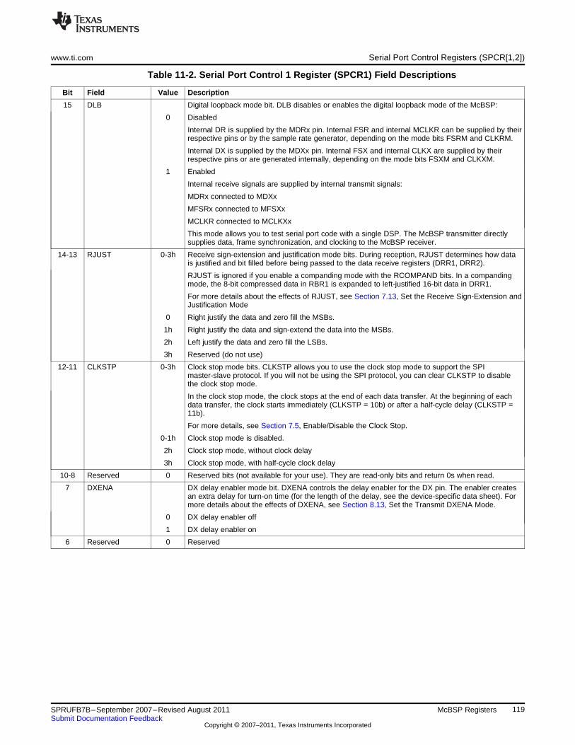
www.ti.com Serial Port Control Registers (SPCR[1,2])
Table 11-2. Serial Port Control 1 Register (SPCR1) Field Descriptions
Bit Field Value Description
15 DLB Digital loopback mode bit. DLB disables or enables the digital loopback mode of the McBSP:
0 Disabled
Internal DR is supplied by the MDRx pin. Internal FSR and internal MCLKR can be supplied by theirrespective pins or by the sample rate generator, depending on the mode bits FSRM and CLKRM.
Internal DX is supplied by the MDXx pin. Internal FSX and internal CLKX are supplied by theirrespective pins or are generated internally, depending on the mode bits FSXM and CLKXM.
1 Enabled
Internal receive signals are supplied by internal transmit signals:
MDRx connected to MDXx
MFSRx connected to MFSXx
MCLKR connected to MCLKXx
This mode allows you to test serial port code with a single DSP. The McBSP transmitter directlysupplies data, frame synchronization, and clocking to the McBSP receiver.
14-13 RJUST 0-3h Receive sign-extension and justification mode bits. During reception, RJUST determines how datais justified and bit filled before being passed to the data receive registers (DRR1, DRR2).
RJUST is ignored if you enable a companding mode with the RCOMPAND bits. In a compandingmode, the 8-bit compressed data in RBR1 is expanded to left-justified 16-bit data in DRR1.
For more details about the effects of RJUST, see Section 7.13, Set the Receive Sign-Extension andJustification Mode
0 Right justify the data and zero fill the MSBs.
1h Right justify the data and sign-extend the data into the MSBs.
2h Left justify the data and zero fill the LSBs.
3h Reserved (do not use)
12-11 CLKSTP 0-3h Clock stop mode bits. CLKSTP allows you to use the clock stop mode to support the SPImaster-slave protocol. If you will not be using the SPI protocol, you can clear CLKSTP to disablethe clock stop mode.
In the clock stop mode, the clock stops at the end of each data transfer. At the beginning of eachdata transfer, the clock starts immediately (CLKSTP = 10b) or after a half-cycle delay (CLKSTP =11b).
For more details, see Section 7.5, Enable/Disable the Clock Stop.
0-1h Clock stop mode is disabled.
2h Clock stop mode, without clock delay
3h Clock stop mode, with half-cycle clock delay
10-8 Reserved 0 Reserved bits (not available for your use). They are read-only bits and return 0s when read.
7 DXENA DX delay enabler mode bit. DXENA controls the delay enabler for the DX pin. The enabler createsan extra delay for turn-on time (for the length of the delay, see the device-specific data sheet). Formore details about the effects of DXENA, see Section 8.13, Set the Transmit DXENA Mode.
0 DX delay enabler off
1 DX delay enabler on
6 Reserved 0 Reserved
119SPRUFB7B–September 2007–Revised August 2011 McBSP RegistersSubmit Documentation Feedback
Copyright © 2007–2011, Texas Instruments Incorporated
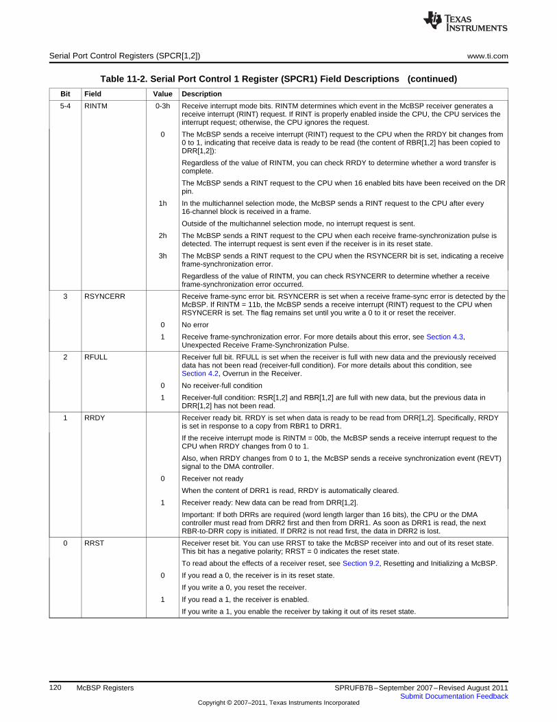
Serial Port Control Registers (SPCR[1,2]) www.ti.com
Table 11-2. Serial Port Control 1 Register (SPCR1) Field Descriptions (continued)
Bit Field Value Description
5-4 RINTM 0-3h Receive interrupt mode bits. RINTM determines which event in the McBSP receiver generates areceive interrupt (RINT) request. If RINT is properly enabled inside the CPU, the CPU services theinterrupt request; otherwise, the CPU ignores the request.
0 The McBSP sends a receive interrupt (RINT) request to the CPU when the RRDY bit changes from0 to 1, indicating that receive data is ready to be read (the content of RBR[1,2] has been copied toDRR[1,2]):
Regardless of the value of RINTM, you can check RRDY to determine whether a word transfer iscomplete.
The McBSP sends a RINT request to the CPU when 16 enabled bits have been received on the DRpin.
1h In the multichannel selection mode, the McBSP sends a RINT request to the CPU after every16-channel block is received in a frame.
Outside of the multichannel selection mode, no interrupt request is sent.
2h The McBSP sends a RINT request to the CPU when each receive frame-synchronization pulse isdetected. The interrupt request is sent even if the receiver is in its reset state.
3h The McBSP sends a RINT request to the CPU when the RSYNCERR bit is set, indicating a receiveframe-synchronization error.
Regardless of the value of RINTM, you can check RSYNCERR to determine whether a receiveframe-synchronization error occurred.
3 RSYNCERR Receive frame-sync error bit. RSYNCERR is set when a receive frame-sync error is detected by theMcBSP. If RINTM = 11b, the McBSP sends a receive interrupt (RINT) request to the CPU whenRSYNCERR is set. The flag remains set until you write a 0 to it or reset the receiver.
0 No error
1 Receive frame-synchronization error. For more details about this error, see Section 4.3,Unexpected Receive Frame-Synchronization Pulse.
2 RFULL Receiver full bit. RFULL is set when the receiver is full with new data and the previously receiveddata has not been read (receiver-full condition). For more details about this condition, seeSection 4.2, Overrun in the Receiver.
0 No receiver-full condition
1 Receiver-full condition: RSR[1,2] and RBR[1,2] are full with new data, but the previous data inDRR[1,2] has not been read.
1 RRDY Receiver ready bit. RRDY is set when data is ready to be read from DRR[1,2]. Specifically, RRDYis set in response to a copy from RBR1 to DRR1.
If the receive interrupt mode is RINTM = 00b, the McBSP sends a receive interrupt request to theCPU when RRDY changes from 0 to 1.
Also, when RRDY changes from 0 to 1, the McBSP sends a receive synchronization event (REVT)signal to the DMA controller.
0 Receiver not ready
When the content of DRR1 is read, RRDY is automatically cleared.
1 Receiver ready: New data can be read from DRR[1,2].
Important: If both DRRs are required (word length larger than 16 bits), the CPU or the DMAcontroller must read from DRR2 first and then from DRR1. As soon as DRR1 is read, the nextRBR-to-DRR copy is initiated. If DRR2 is not read first, the data in DRR2 is lost.
0 RRST Receiver reset bit. You can use RRST to take the McBSP receiver into and out of its reset state.This bit has a negative polarity; RRST = 0 indicates the reset state.
To read about the effects of a receiver reset, see Section 9.2, Resetting and Initializing a McBSP.
0 If you read a 0, the receiver is in its reset state.
If you write a 0, you reset the receiver.
1 If you read a 1, the receiver is enabled.
If you write a 1, you enable the receiver by taking it out of its reset state.
120 McBSP Registers SPRUFB7B–September 2007–Revised August 2011Submit Documentation Feedback
Copyright © 2007–2011, Texas Instruments Incorporated
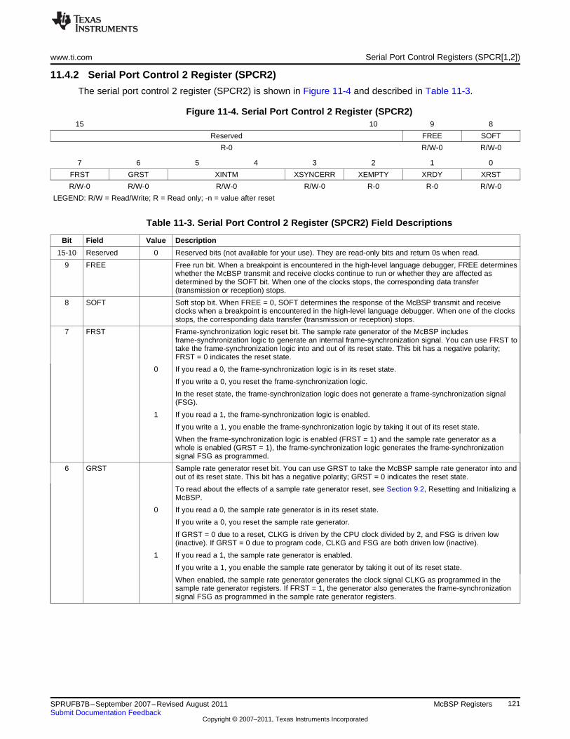
www.ti.com Serial Port Control Registers (SPCR[1,2])
11.4.2 Serial Port Control 2 Register (SPCR2)
The serial port control 2 register (SPCR2) is shown in Figure 11-4 and described in Table 11-3.
Figure 11-4. Serial Port Control 2 Register (SPCR2)15 10 9 8
Reserved FREE SOFT
R-0 R/W-0 R/W-0
7 6 5 4 3 2 1 0
FRST GRST XINTM XSYNCERR XEMPTY XRDY XRST
R/W-0 R/W-0 R/W-0 R/W-0 R-0 R-0 R/W-0
LEGEND: R/W = Read/Write; R = Read only; -n = value after reset
Table 11-3. Serial Port Control 2 Register (SPCR2) Field Descriptions
Bit Field Value Description
15-10 Reserved 0 Reserved bits (not available for your use). They are read-only bits and return 0s when read.
9 FREE Free run bit. When a breakpoint is encountered in the high-level language debugger, FREE determineswhether the McBSP transmit and receive clocks continue to run or whether they are affected asdetermined by the SOFT bit. When one of the clocks stops, the corresponding data transfer(transmission or reception) stops.
8 SOFT Soft stop bit. When FREE = 0, SOFT determines the response of the McBSP transmit and receiveclocks when a breakpoint is encountered in the high-level language debugger. When one of the clocksstops, the corresponding data transfer (transmission or reception) stops.
7 FRST Frame-synchronization logic reset bit. The sample rate generator of the McBSP includesframe-synchronization logic to generate an internal frame-synchronization signal. You can use FRST totake the frame-synchronization logic into and out of its reset state. This bit has a negative polarity;FRST = 0 indicates the reset state.
0 If you read a 0, the frame-synchronization logic is in its reset state.
If you write a 0, you reset the frame-synchronization logic.
In the reset state, the frame-synchronization logic does not generate a frame-synchronization signal(FSG).
1 If you read a 1, the frame-synchronization logic is enabled.
If you write a 1, you enable the frame-synchronization logic by taking it out of its reset state.
When the frame-synchronization logic is enabled (FRST = 1) and the sample rate generator as awhole is enabled (GRST = 1), the frame-synchronization logic generates the frame-synchronizationsignal FSG as programmed.
6 GRST Sample rate generator reset bit. You can use GRST to take the McBSP sample rate generator into andout of its reset state. This bit has a negative polarity; GRST = 0 indicates the reset state.
To read about the effects of a sample rate generator reset, see Section 9.2, Resetting and Initializing aMcBSP.
0 If you read a 0, the sample rate generator is in its reset state.
If you write a 0, you reset the sample rate generator.
If GRST = 0 due to a reset, CLKG is driven by the CPU clock divided by 2, and FSG is driven low(inactive). If GRST = 0 due to program code, CLKG and FSG are both driven low (inactive).
1 If you read a 1, the sample rate generator is enabled.
If you write a 1, you enable the sample rate generator by taking it out of its reset state.
When enabled, the sample rate generator generates the clock signal CLKG as programmed in thesample rate generator registers. If FRST = 1, the generator also generates the frame-synchronizationsignal FSG as programmed in the sample rate generator registers.
121SPRUFB7B–September 2007–Revised August 2011 McBSP RegistersSubmit Documentation Feedback
Copyright © 2007–2011, Texas Instruments Incorporated
Serial Port Control Registers (SPCR[1,2]) www.ti.com
Table 11-3. Serial Port Control 2 Register (SPCR2) Field Descriptions (continued)
Bit Field Value Description
5-4 XINTM 0-3h Transmit interrupt mode bits. XINTM determines which event in the McBSP transmitter generates atransmit interrupt (XINT) request. If XINT is properly enabled, the CPU services the interrupt request;otherwise, the CPU ignores the request.
0 The McBSP sends a transmit interrupt (XINT) request to the CPU when the XRDY bit changes from 0to 1, indicating that transmitter is ready to accept new data (the content of DXR[1,2] has been copiedto XSR[1,2]).
Regardless of the value of XINTM, you can check XRDY to determine whether a word transfer iscomplete.
The McBSP sends an XINT request to the CPU when 16 enabled bits have been transmitted on theDX pin.
1h In the multichannel selection mode, the McBSP sends an XINT request to the CPU after every16-channel block is transmitted in a frame.
Outside of the multichannel selection mode, no interrupt request is sent.
2h The McBSP sends an XINT request to the CPU when each transmit frame-synchronization pulse isdetected. The interrupt request is sent even if the transmitter is in its reset state.
3h The McBSP sends an XINT request to the CPU when the XSYNCERR bit is set, indicating a transmitframe-synchronization error.
Regardless of the value of XINTM, you can check XSYNCERR to determine whether a transmitframe-synchronization error occurred.
3 XSYNCERR Transmit frame-synchronization error bit. XSYNCERR is set when a transmit frame-synchronizationerror is detected by the McBSP. If XINTM = 11b, the McBSP sends a transmit interrupt (XINT) requestto the CPU when XSYNCERR is set. The flag remains set until you write a 0 to it or reset thetransmitter.
If XINTM = 11b, writing a 1 to XSYNCERR triggers a transmit interrupt just as if a transmitframe-synchronization error occurred.
For details about this error see Section 4.6, Unexpected Transmit Frame-Synchronization Pulse.
0 No error
1 Transmit frame-synchronization error
2 XEMPTY Transmitter empty bit. XEMPTY is cleared when the transmitter is ready to send new data but no newdata is available (transmitter-empty condition). This bit has a negative polarity; a transmitter-emptycondition is indicated by XEMPTY = 0.
0 Transmitter-empty condition
Typically this indicates that all the bits of the current word have been transmitted but there is no newdata in DXR1. XEMPTY is also cleared if the transmitter is reset and then restarted.
For more details about this error condition, see Section 4.5, Underflow in the Transmitter.
1 No transmitter-empty condition
1 XRDY Transmitter ready bit. XRDY is set when the transmitter is ready to accept new data in DXR[1,2].Specifically, XRDY is set in response to a copy from DXR1 to XSR1.
If the transmit interrupt mode is XINTM = 00b, the McBSP sends a transmit interrupt (XINT) request tothe CPU when XRDY changes from 0 to 1.
Also, when XRDY changes from 0 to 1, the McBSP sends a transmit synchronization event (XEVT)signal to the DMA controller.
0 Transmitter not ready
When DXR1 is loaded, XRDY is automatically cleared.
1 Transmitter ready: DXR[1,2] is ready to accept new data.
If both DXRs are needed (word length larger than 16 bits), the CPU or the DMA controller must loadDXR2 first and then load DXR1. As soon as DXR1 is loaded, the contents of both DXRs are copied tothe transmit shift registers (XSRs), as described in the next step. If DXR2 is not loaded first, theprevious content of DXR2 is passed to the XSR2.
122 McBSP Registers SPRUFB7B–September 2007–Revised August 2011Submit Documentation Feedback
Copyright © 2007–2011, Texas Instruments Incorporated
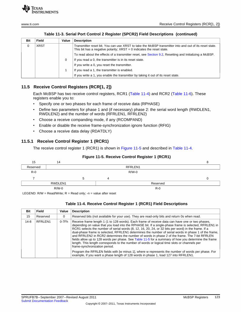
www.ti.com Receive Control Registers (RCR[1, 2])
Table 11-3. Serial Port Control 2 Register (SPCR2) Field Descriptions (continued)
Bit Field Value Description
0 XRST Transmitter reset bit. You can use XRST to take the McBSP transmitter into and out of its reset state.This bit has a negative polarity; XRST = 0 indicates the reset state.
To read about the effects of a transmitter reset, see Section 9.2, Resetting and Initializing a McBSP.
0 If you read a 0, the transmitter is in its reset state.
If you write a 0, you reset the transmitter.
1 If you read a 1, the transmitter is enabled.
If you write a 1, you enable the transmitter by taking it out of its reset state.
11.5 Receive Control Registers (RCR[1, 2])
Each McBSP has two receive control registers, RCR1 (Table 11-4) and RCR2 (Table 11-6). Theseregisters enable you to:
• Specify one or two phases for each frame of receive data (RPHASE)
• Define two parameters for phase 1 and (if necessary) phase 2: the serial word length (RWDLEN1,RWDLEN2) and the number of words (RFRLEN1, RFRLEN2)
• Choose a receive companding mode, if any (RCOMPAND)
• Enable or disable the receive frame-synchronization ignore function (RFIG)
• Choose a receive data delay (RDATDLY)
11.5.1 Receive Control Register 1 (RCR1)
The receive control register 1 (RCR1) is shown in Figure 11-5 and described in Table 11-4.
Figure 11-5. Receive Control Register 1 (RCR1)15 14 8
Reserved RFRLEN1
R-0 R/W-0
7 5 4 0
RWDLEN1 Reserved
R/W-0 R-0
LEGEND: R/W = Read/Write; R = Read only; -n = value after reset
Table 11-4. Receive Control Register 1 (RCR1) Field Descriptions
Bit Field Value Description
15 Reserved 0 Reserved bits (not available for your use). They are read-only bits and return 0s when read.
14-8 RFRLEN1 0-7Fh Receive frame length 1 (1 to 128 words). Each frame of receive data can have one or two phases,depending on value that you load into the RPHASE bit. If a single-phase frame is selected, RFRLEN1 inRCR1 selects the number of serial words (8, 12, 16, 20, 24, or 32 bits per word) in the frame. If adual-phase frame is selected, RFRLEN1 determines the number of serial words in phase 1 of the frame,and RFRLEN2 in RCR2 determines the number of words in phase 2 of the frame. The 7-bit RFRLENfields allow up to 128 words per phase. See Table 11-5 for a summary of how you determine the framelength. This length corresponds to the number of words or logical time slots or channels perframe-synchronization period.
Program the RFRLEN fields with [w minus 1], where w represents the number of words per phase. Forexample, if you want a phase length of 128 words in phase 1, load 127 into RFRLEN1.
123SPRUFB7B–September 2007–Revised August 2011 McBSP RegistersSubmit Documentation Feedback
Copyright © 2007–2011, Texas Instruments Incorporated
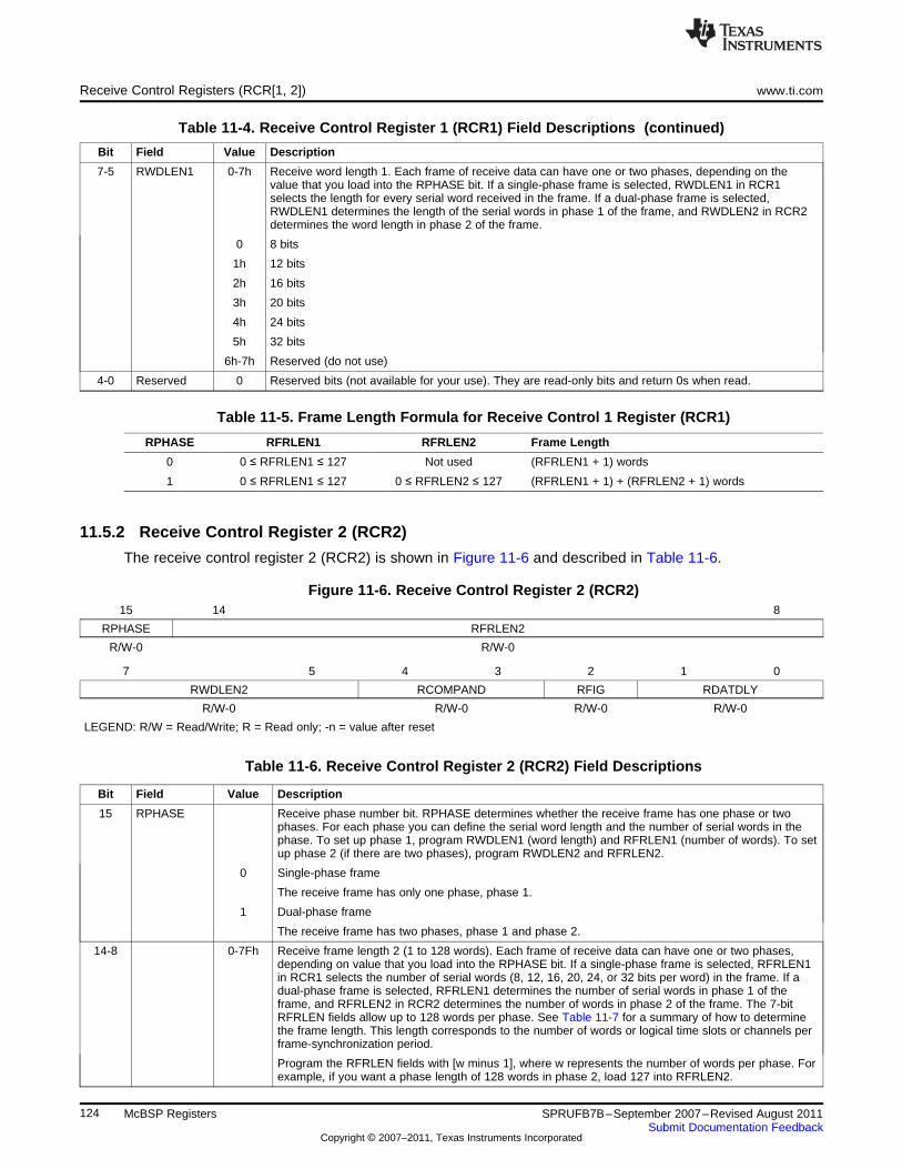
Receive Control Registers (RCR[1, 2]) www.ti.com
Table 11-4. Receive Control Register 1 (RCR1) Field Descriptions (continued)
Bit Field Value Description
7-5 RWDLEN1 0-7h Receive word length 1. Each frame of receive data can have one or two phases, depending on thevalue that you load into the RPHASE bit. If a single-phase frame is selected, RWDLEN1 in RCR1selects the length for every serial word received in the frame. If a dual-phase frame is selected,RWDLEN1 determines the length of the serial words in phase 1 of the frame, and RWDLEN2 in RCR2determines the word length in phase 2 of the frame.
0 8 bits
1h 12 bits
2h 16 bits
3h 20 bits
4h 24 bits
5h 32 bits
6h-7h Reserved (do not use)
4-0 Reserved 0 Reserved bits (not available for your use). They are read-only bits and return 0s when read.
Table 11-5. Frame Length Formula for Receive Control 1 Register (RCR1)
RPHASE RFRLEN1 RFRLEN2 Frame Length
0 0 ≤ RFRLEN1 ≤ 127 Not used (RFRLEN1 + 1) words
1 0 ≤ RFRLEN1 ≤ 127 0 ≤ RFRLEN2 ≤ 127 (RFRLEN1 + 1) + (RFRLEN2 + 1) words
11.5.2 Receive Control Register 2 (RCR2)
The receive control register 2 (RCR2) is shown in Figure 11-6 and described in Table 11-6.
Figure 11-6. Receive Control Register 2 (RCR2)15 14 8
RPHASE RFRLEN2
R/W-0 R/W-0
7 5 4 3 2 1 0
RWDLEN2 RCOMPAND RFIG RDATDLY
R/W-0 R/W-0 R/W-0 R/W-0
LEGEND: R/W = Read/Write; R = Read only; -n = value after reset
Table 11-6. Receive Control Register 2 (RCR2) Field Descriptions
Bit Field Value Description
15 RPHASE Receive phase number bit. RPHASE determines whether the receive frame has one phase or twophases. For each phase you can define the serial word length and the number of serial words in thephase. To set up phase 1, program RWDLEN1 (word length) and RFRLEN1 (number of words). To setup phase 2 (if there are two phases), program RWDLEN2 and RFRLEN2.
0 Single-phase frame
The receive frame has only one phase, phase 1.
1 Dual-phase frame
The receive frame has two phases, phase 1 and phase 2.
14-8 0-7Fh Receive frame length 2 (1 to 128 words). Each frame of receive data can have one or two phases,depending on value that you load into the RPHASE bit. If a single-phase frame is selected, RFRLEN1in RCR1 selects the number of serial words (8, 12, 16, 20, 24, or 32 bits per word) in the frame. If adual-phase frame is selected, RFRLEN1 determines the number of serial words in phase 1 of theframe, and RFRLEN2 in RCR2 determines the number of words in phase 2 of the frame. The 7-bitRFRLEN fields allow up to 128 words per phase. See Table 11-7 for a summary of how to determinethe frame length. This length corresponds to the number of words or logical time slots or channels perframe-synchronization period.
Program the RFRLEN fields with [w minus 1], where w represents the number of words per phase. Forexample, if you want a phase length of 128 words in phase 2, load 127 into RFRLEN2.
124 McBSP Registers SPRUFB7B–September 2007–Revised August 2011Submit Documentation Feedback
Copyright © 2007–2011, Texas Instruments Incorporated
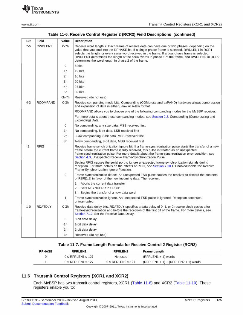
www.ti.com Transmit Control Registers (XCR1 and XCR2)
Table 11-6. Receive Control Register 2 (RCR2) Field Descriptions (continued)
Bit Field Value Description
7-5 RWDLEN2 0-7h Receive word length 2. Each frame of receive data can have one or two phases, depending on thevalue that you load into the RPHASE bit. If a single-phase frame is selected, RWDLEN1 in RCR1selects the length for every serial word received in the frame. If a dual-phase frame is selected,RWDLEN1 determines the length of the serial words in phase 1 of the frame, and RWDLEN2 in RCR2determines the word length in phase 2 of the frame.
0 8 bits
1h 12 bits
2h 16 bits
3h 20 bits
4h 24 bits
5h 32 bits
6h-7h Reserved (do not use)
4-3 RCOMPAND 0-3h Receive companding mode bits. Companding (COMpress and exPAND) hardware allows compressionand expansion of data in either μ-law or A-law format.
RCOMPAND allows you to choose one of the following companding modes for the McBSP receiver:
For more details about these companding modes, see Section 2.2, Companding (Compressing andExpanding) Data.
0 No companding, any size data, MSB received first
1h No companding, 8-bit data, LSB received first
2h μ-law companding, 8-bit data, MSB received first
3h A-law companding, 8-bit data, MSB received first
2 RFIG Receive frame-synchronization ignore bit. If a frame-synchronization pulse starts the transfer of a newframe before the current frame is fully received, this pulse is treated as an unexpectedframe-synchronization pulse. For more details about the frame-synchronization error condition, seeSection 4.3, Unexpected Receive Frame-Synchronization Pulse.
Setting RFIG causes the serial port to ignore unexpected frame-synchronization signals duringreception. For more details on the effects of RFIG, see Section 7.10.1, Enable/Disable the ReceiveFrame-Synchronization Ignore Function.
0 Frame-synchronization detect. An unexpected FSR pulse causes the receiver to discard the contentsof RSR[1,2] in favor of the new incoming data. The receiver:
1. Aborts the current data transfer2. Sets RSYNCERR in SPCR13. Begins the transfer of a new data word
1 Frame-synchronization ignore. An unexpected FSR pulse is ignored. Reception continuesuninterrupted.
1-0 RDATDLY 0-3h Receive data delay bits. RDATDLY specifies a data delay of 0, 1, or 2 receive clock cycles afterframe-synchronization and before the reception of the first bit of the frame. For more details, seeSection 7.12, Set the Receive Data Delay.
0 0-bit data delay
1h 1-bit data delay
2h 2-bit data delay
3h Reserved (do not use)
Table 11-7. Frame Length Formula for Receive Control 2 Register (RCR2)
RPHASE RFRLEN1 RFRLEN2 Frame Length
0 0 ≤ RFRLEN1 ≤ 127 Not used (RFRLEN1 + 1) words
1 0 ≤ RFRLEN1 ≤ 127 0 ≤ RFRLEN2 ≤ 127 (RFRLEN1 + 1) + (RFRLEN2 + 1) words
11.6 Transmit Control Registers (XCR1 and XCR2)
Each McBSP has two transmit control registers, XCR1 (Table 11-8) and XCR2 (Table 11-10). Theseregisters enable you to:
125SPRUFB7B–September 2007–Revised August 2011 McBSP RegistersSubmit Documentation Feedback
Copyright © 2007–2011, Texas Instruments Incorporated
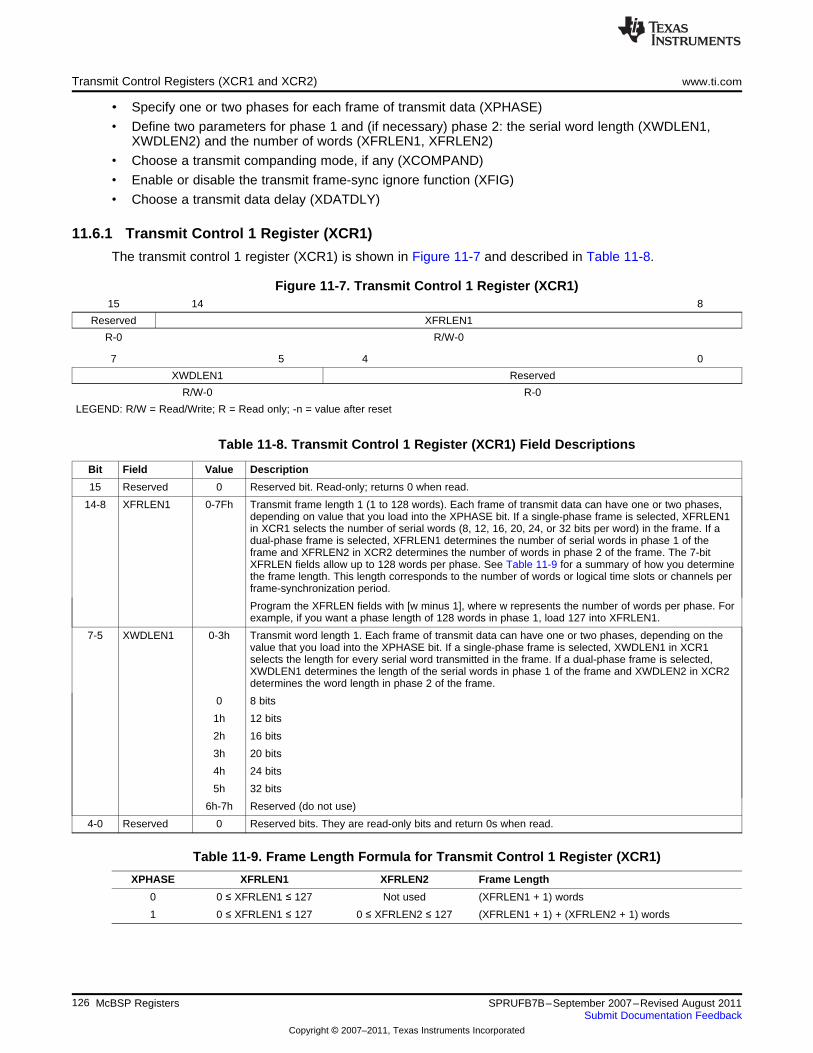
Transmit Control Registers (XCR1 and XCR2) www.ti.com
• Specify one or two phases for each frame of transmit data (XPHASE)
• Define two parameters for phase 1 and (if necessary) phase 2: the serial word length (XWDLEN1,XWDLEN2) and the number of words (XFRLEN1, XFRLEN2)
• Choose a transmit companding mode, if any (XCOMPAND)
• Enable or disable the transmit frame-sync ignore function (XFIG)
• Choose a transmit data delay (XDATDLY)
11.6.1 Transmit Control 1 Register (XCR1)
The transmit control 1 register (XCR1) is shown in Figure 11-7 and described in Table 11-8.
Figure 11-7. Transmit Control 1 Register (XCR1)15 14 8
Reserved XFRLEN1
R-0 R/W-0
7 5 4 0
XWDLEN1 Reserved
R/W-0 R-0
LEGEND: R/W = Read/Write; R = Read only; -n = value after reset
Table 11-8. Transmit Control 1 Register (XCR1) Field Descriptions
Bit Field Value Description
15 Reserved 0 Reserved bit. Read-only; returns 0 when read.
14-8 XFRLEN1 0-7Fh Transmit frame length 1 (1 to 128 words). Each frame of transmit data can have one or two phases,depending on value that you load into the XPHASE bit. If a single-phase frame is selected, XFRLEN1in XCR1 selects the number of serial words (8, 12, 16, 20, 24, or 32 bits per word) in the frame. If adual-phase frame is selected, XFRLEN1 determines the number of serial words in phase 1 of theframe and XFRLEN2 in XCR2 determines the number of words in phase 2 of the frame. The 7-bitXFRLEN fields allow up to 128 words per phase. See Table 11-9 for a summary of how you determinethe frame length. This length corresponds to the number of words or logical time slots or channels perframe-synchronization period.
Program the XFRLEN fields with [w minus 1], where w represents the number of words per phase. Forexample, if you want a phase length of 128 words in phase 1, load 127 into XFRLEN1.
7-5 XWDLEN1 0-3h Transmit word length 1. Each frame of transmit data can have one or two phases, depending on thevalue that you load into the XPHASE bit. If a single-phase frame is selected, XWDLEN1 in XCR1selects the length for every serial word transmitted in the frame. If a dual-phase frame is selected,XWDLEN1 determines the length of the serial words in phase 1 of the frame and XWDLEN2 in XCR2determines the word length in phase 2 of the frame.
0 8 bits
1h 12 bits
2h 16 bits
3h 20 bits
4h 24 bits
5h 32 bits
6h-7h Reserved (do not use)
4-0 Reserved 0 Reserved bits. They are read-only bits and return 0s when read.
Table 11-9. Frame Length Formula for Transmit Control 1 Register (XCR1)
XPHASE XFRLEN1 XFRLEN2 Frame Length
0 0 ≤ XFRLEN1 ≤ 127 Not used (XFRLEN1 + 1) words
1 0 ≤ XFRLEN1 ≤ 127 0 ≤ XFRLEN2 ≤ 127 (XFRLEN1 + 1) + (XFRLEN2 + 1) words
126 McBSP Registers SPRUFB7B–September 2007–Revised August 2011Submit Documentation Feedback
Copyright © 2007–2011, Texas Instruments Incorporated
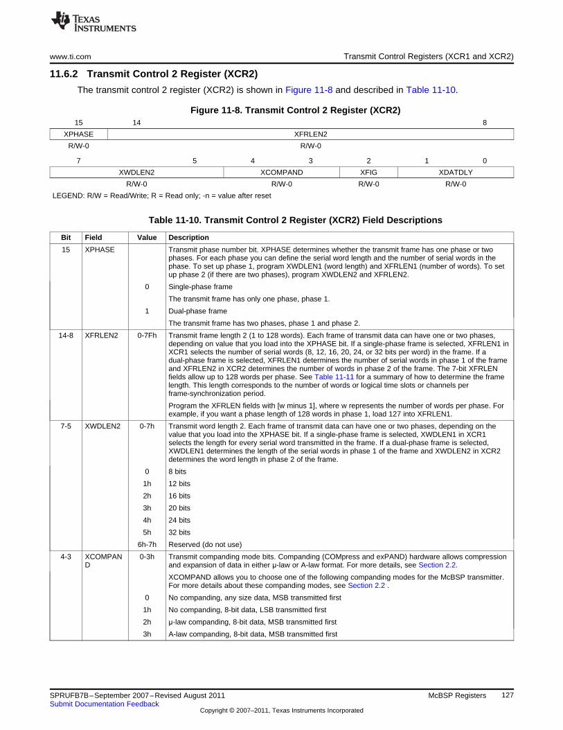
www.ti.com Transmit Control Registers (XCR1 and XCR2)
11.6.2 Transmit Control 2 Register (XCR2)
The transmit control 2 register (XCR2) is shown in Figure 11-8 and described in Table 11-10.
Figure 11-8. Transmit Control 2 Register (XCR2)15 14 8
XPHASE XFRLEN2
R/W-0 R/W-0
7 5 4 3 2 1 0
XWDLEN2 XCOMPAND XFIG XDATDLY
R/W-0 R/W-0 R/W-0 R/W-0
LEGEND: R/W = Read/Write; R = Read only; -n = value after reset
Table 11-10. Transmit Control 2 Register (XCR2) Field Descriptions
Bit Field Value Description
15 XPHASE Transmit phase number bit. XPHASE determines whether the transmit frame has one phase or twophases. For each phase you can define the serial word length and the number of serial words in thephase. To set up phase 1, program XWDLEN1 (word length) and XFRLEN1 (number of words). To setup phase 2 (if there are two phases), program XWDLEN2 and XFRLEN2.
0 Single-phase frame
The transmit frame has only one phase, phase 1.
1 Dual-phase frame
The transmit frame has two phases, phase 1 and phase 2.
14-8 XFRLEN2 0-7Fh Transmit frame length 2 (1 to 128 words). Each frame of transmit data can have one or two phases,depending on value that you load into the XPHASE bit. If a single-phase frame is selected, XFRLEN1 inXCR1 selects the number of serial words (8, 12, 16, 20, 24, or 32 bits per word) in the frame. If adual-phase frame is selected, XFRLEN1 determines the number of serial words in phase 1 of the frameand XFRLEN2 in XCR2 determines the number of words in phase 2 of the frame. The 7-bit XFRLENfields allow up to 128 words per phase. See Table 11-11 for a summary of how to determine the framelength. This length corresponds to the number of words or logical time slots or channels perframe-synchronization period.
Program the XFRLEN fields with [w minus 1], where w represents the number of words per phase. Forexample, if you want a phase length of 128 words in phase 1, load 127 into XFRLEN1.
7-5 XWDLEN2 0-7h Transmit word length 2. Each frame of transmit data can have one or two phases, depending on thevalue that you load into the XPHASE bit. If a single-phase frame is selected, XWDLEN1 in XCR1selects the length for every serial word transmitted in the frame. If a dual-phase frame is selected,XWDLEN1 determines the length of the serial words in phase 1 of the frame and XWDLEN2 in XCR2determines the word length in phase 2 of the frame.
0 8 bits
1h 12 bits
2h 16 bits
3h 20 bits
4h 24 bits
5h 32 bits
6h-7h Reserved (do not use)
4-3 XCOMPAN 0-3h Transmit companding mode bits. Companding (COMpress and exPAND) hardware allows compressionD and expansion of data in either μ-law or A-law format. For more details, see Section 2.2.
XCOMPAND allows you to choose one of the following companding modes for the McBSP transmitter.For more details about these companding modes, see Section 2.2 .
0 No companding, any size data, MSB transmitted first
1h No companding, 8-bit data, LSB transmitted first
2h μ-law companding, 8-bit data, MSB transmitted first
3h A-law companding, 8-bit data, MSB transmitted first
127SPRUFB7B–September 2007–Revised August 2011 McBSP RegistersSubmit Documentation Feedback
Copyright © 2007–2011, Texas Instruments Incorporated
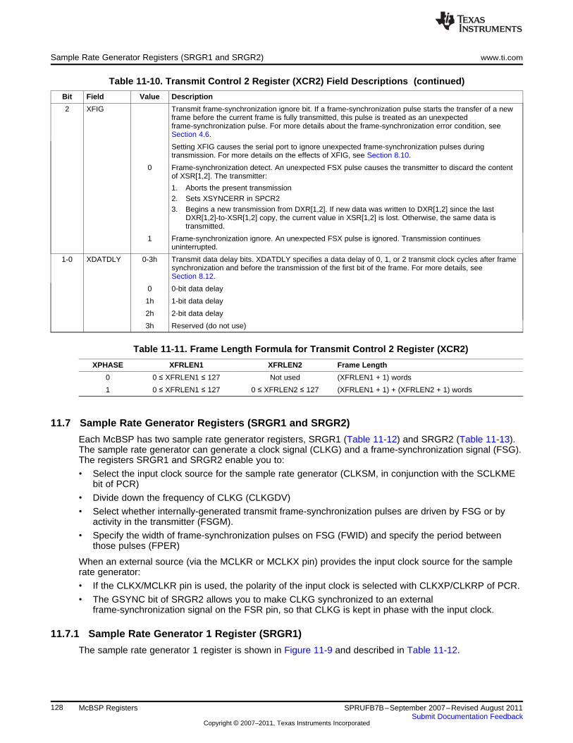
Sample Rate Generator Registers (SRGR1 and SRGR2) www.ti.com
Table 11-10. Transmit Control 2 Register (XCR2) Field Descriptions (continued)
Bit Field Value Description
2 XFIG Transmit frame-synchronization ignore bit. If a frame-synchronization pulse starts the transfer of a newframe before the current frame is fully transmitted, this pulse is treated as an unexpectedframe-synchronization pulse. For more details about the frame-synchronization error condition, seeSection 4.6.
Setting XFIG causes the serial port to ignore unexpected frame-synchronization pulses duringtransmission. For more details on the effects of XFIG, see Section 8.10.
0 Frame-synchronization detect. An unexpected FSX pulse causes the transmitter to discard the contentof XSR[1,2]. The transmitter:
1. Aborts the present transmission2. Sets XSYNCERR in SPCR23. Begins a new transmission from DXR[1,2]. If new data was written to DXR[1,2] since the last
DXR[1,2]-to-XSR[1,2] copy, the current value in XSR[1,2] is lost. Otherwise, the same data istransmitted.
1 Frame-synchronization ignore. An unexpected FSX pulse is ignored. Transmission continuesuninterrupted.
1-0 XDATDLY 0-3h Transmit data delay bits. XDATDLY specifies a data delay of 0, 1, or 2 transmit clock cycles after framesynchronization and before the transmission of the first bit of the frame. For more details, seeSection 8.12.
0 0-bit data delay
1h 1-bit data delay
2h 2-bit data delay
3h Reserved (do not use)
Table 11-11. Frame Length Formula for Transmit Control 2 Register (XCR2)
XPHASE XFRLEN1 XFRLEN2 Frame Length
0 0 ≤ XFRLEN1 ≤ 127 Not used (XFRLEN1 + 1) words
1 0 ≤ XFRLEN1 ≤ 127 0 ≤ XFRLEN2 ≤ 127 (XFRLEN1 + 1) + (XFRLEN2 + 1) words
11.7 Sample Rate Generator Registers (SRGR1 and SRGR2)
Each McBSP has two sample rate generator registers, SRGR1 (Table 11-12) and SRGR2 (Table 11-13).The sample rate generator can generate a clock signal (CLKG) and a frame-synchronization signal (FSG).The registers SRGR1 and SRGR2 enable you to:
• Select the input clock source for the sample rate generator (CLKSM, in conjunction with the SCLKMEbit of PCR)
• Divide down the frequency of CLKG (CLKGDV)
• Select whether internally-generated transmit frame-synchronization pulses are driven by FSG or byactivity in the transmitter (FSGM).
• Specify the width of frame-synchronization pulses on FSG (FWID) and specify the period betweenthose pulses (FPER)
When an external source (via the MCLKR or MCLKX pin) provides the input clock source for the samplerate generator:
• If the CLKX/MCLKR pin is used, the polarity of the input clock is selected with CLKXP/CLKRP of PCR.
• The GSYNC bit of SRGR2 allows you to make CLKG synchronized to an externalframe-synchronization signal on the FSR pin, so that CLKG is kept in phase with the input clock.
11.7.1 Sample Rate Generator 1 Register (SRGR1)
The sample rate generator 1 register is shown in Figure 11-9 and described in Table 11-12.
128 McBSP Registers SPRUFB7B–September 2007–Revised August 2011Submit Documentation Feedback
Copyright © 2007–2011, Texas Instruments Incorporated
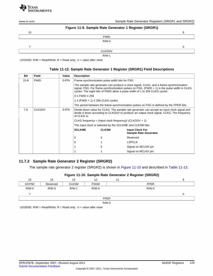
www.ti.com Sample Rate Generator Registers (SRGR1 and SRGR2)
Figure 11-9. Sample Rate Generator 1 Register (SRGR1)15 8
FWID
R/W-0
7 0
CLKGDV
R/W-1
LEGEND: R/W = Read/Write; R = Read only; -n = value after reset
Table 11-12. Sample Rate Generator 1 Register (SRGR1) Field Descriptions
Bit Field Value Description
15-8 FWID 0-FFh Frame-synchronization pulse width bits for FSG
The sample rate generator can produce a clock signal, CLKG, and a frame-synchronizationsignal, FSG. For frame-synchronization pulses on FSG, (FWID + 1) is the pulse width in CLKGcycles. The eight bits of FWID allow a pulse width of 1 to 256 CLKG cycles:
0 ≤ FWID ≤ 255
1 ≤ (FWID + 1) ≤ 256 CLKG cycles
The period between the frame-synchronization pulses on FSG is defined by the FPER bits.
7-0 CLKGDV 0-FFh Divide-down value for CLKG. The sample rate generator can accept an input clock signal anddivide it down according to CLKGDV to produce an output clock signal, CLKG. The frequencyof CLKG is:
CLKG frequency = (Input clock frequency)/ (CLKGDV + 1)
The input clock is selected by the SCLKME and CLKSM bits:
SCLKME CLKSM Input Clock ForSample Rate Generator
0 0 Reserved
0 1 LSPCLK
1 0 Signal on MCLKR pin
1 1 Signal on MCLKX pin
11.7.2 Sample Rate Generator 2 Register (SRGR2)
The sample rate generator 2 register (SRGR2) is shown in Figure 11-10 and described in Table 11-13.
Figure 11-10. Sample Rate Generator 2 Register (SRGR2)15 14 13 12 11 8
GSYNC Reserved CLKSM FSGM FPER
R/W-0 R/W-0 R/W-1 R/W-0 R/W-0
7 0
FPER
R/W-0
LEGEND: R/W = Read/Write; R = Read only; -n = value after reset
129SPRUFB7B–September 2007–Revised August 2011 McBSP RegistersSubmit Documentation Feedback
Copyright © 2007–2011, Texas Instruments Incorporated
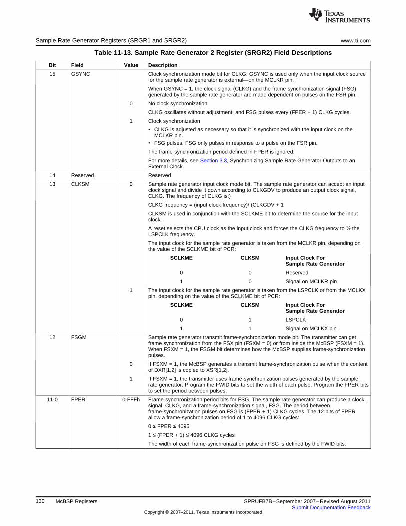
Sample Rate Generator Registers (SRGR1 and SRGR2) www.ti.com
Table 11-13. Sample Rate Generator 2 Register (SRGR2) Field Descriptions
Bit Field Value Description
15 GSYNC Clock synchronization mode bit for CLKG. GSYNC is used only when the input clock sourcefor the sample rate generator is external—on the MCLKR pin.
When GSYNC = 1, the clock signal (CLKG) and the frame-synchronization signal (FSG)generated by the sample rate generator are made dependent on pulses on the FSR pin.
0 No clock synchronization
CLKG oscillates without adjustment, and FSG pulses every (FPER + 1) CLKG cycles.
1 Clock synchronization
• CLKG is adjusted as necessary so that it is synchronized with the input clock on theMCLKR pin.
• FSG pulses. FSG only pulses in response to a pulse on the FSR pin.
The frame-synchronization period defined in FPER is ignored.
For more details, see Section 3.3, Synchronizing Sample Rate Generator Outputs to anExternal Clock.
14 Reserved Reserved
13 CLKSM 0 Sample rate generator input clock mode bit. The sample rate generator can accept an inputclock signal and divide it down according to CLKGDV to produce an output clock signal,CLKG. The frequency of CLKG is:)
CLKG frequency = (input clock frequency)/ (CLKGDV + 1
CLKSM is used in conjunction with the SCLKME bit to determine the source for the inputclock.
A reset selects the CPU clock as the input clock and forces the CLKG frequency to ½ theLSPCLK frequency.
The input clock for the sample rate generator is taken from the MCLKR pin, depending onthe value of the SCLKME bit of PCR:
SCLKME CLKSM Input Clock ForSample Rate Generator
0 0 Reserved
1 0 Signal on MCLKR pin
1 The input clock for the sample rate generator is taken from the LSPCLK or from the MCLKXpin, depending on the value of the SCLKME bit of PCR:
SCLKME CLKSM Input Clock ForSample Rate Generator
0 1 LSPCLK
1 1 Signal on MCLKX pin
12 FSGM Sample rate generator transmit frame-synchronization mode bit. The transmitter can getframe synchronization from the FSX pin (FSXM = 0) or from inside the McBSP (FSXM = 1).When FSXM = 1, the FSGM bit determines how the McBSP supplies frame-synchronizationpulses.
0 If FSXM = 1, the McBSP generates a transmit frame-synchronization pulse when the contentof DXR[1,2] is copied to XSR[1,2].
1 If FSXM = 1, the transmitter uses frame-synchronization pulses generated by the samplerate generator. Program the FWID bits to set the width of each pulse. Program the FPER bitsto set the period between pulses.
11-0 FPER 0-FFFh Frame-synchronization period bits for FSG. The sample rate generator can produce a clocksignal, CLKG, and a frame-synchronization signal, FSG. The period betweenframe-synchronization pulses on FSG is (FPER + 1) CLKG cycles. The 12 bits of FPERallow a frame-synchronization period of 1 to 4096 CLKG cycles:
0 ≤ FPER ≤ 4095
1 ≤ (FPER + 1) ≤ 4096 CLKG cycles
The width of each frame-synchronization pulse on FSG is defined by the FWID bits.
130 McBSP Registers SPRUFB7B–September 2007–Revised August 2011Submit Documentation Feedback
Copyright © 2007–2011, Texas Instruments Incorporated
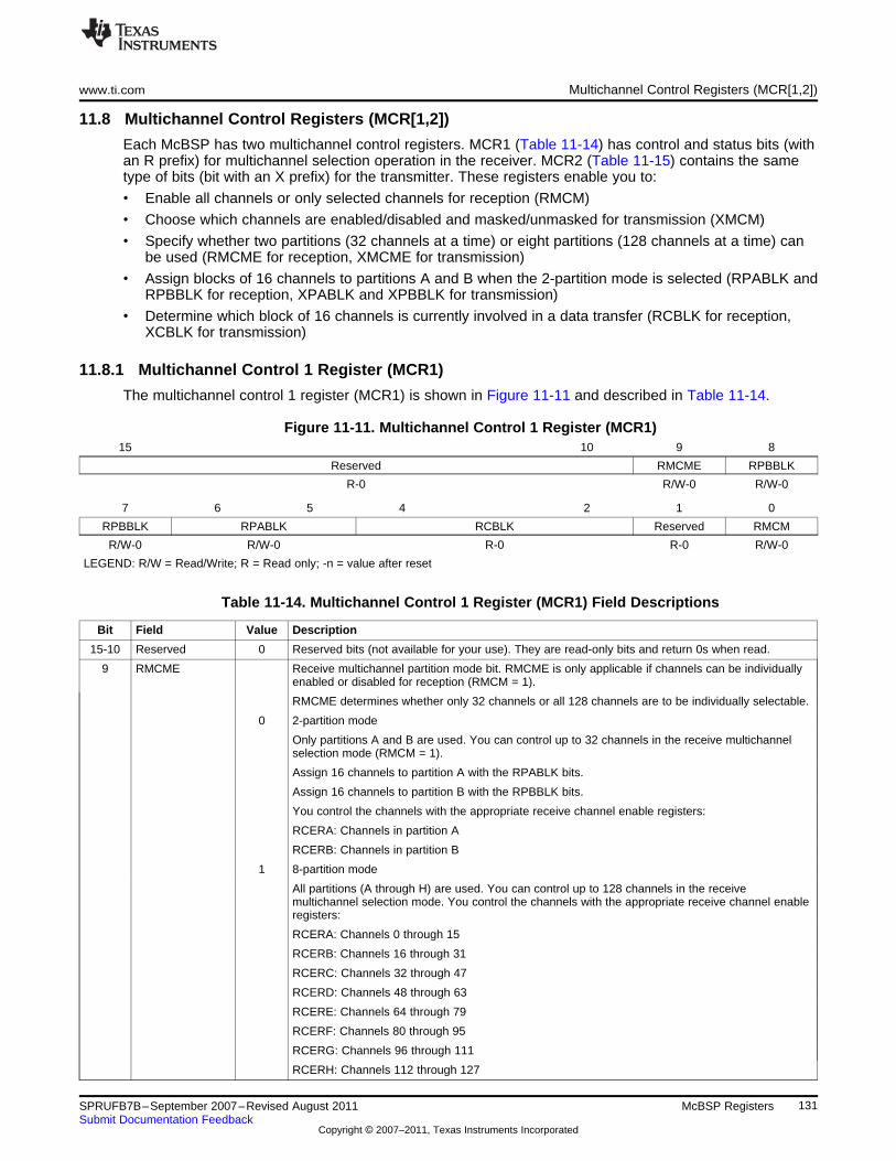
www.ti.com Multichannel Control Registers (MCR[1,2])
11.8 Multichannel Control Registers (MCR[1,2])
Each McBSP has two multichannel control registers. MCR1 (Table 11-14) has control and status bits (withan R prefix) for multichannel selection operation in the receiver. MCR2 (Table 11-15) contains the sametype of bits (bit with an X prefix) for the transmitter. These registers enable you to:
• Enable all channels or only selected channels for reception (RMCM)
• Choose which channels are enabled/disabled and masked/unmasked for transmission (XMCM)
• Specify whether two partitions (32 channels at a time) or eight partitions (128 channels at a time) canbe used (RMCME for reception, XMCME for transmission)
• Assign blocks of 16 channels to partitions A and B when the 2-partition mode is selected (RPABLK andRPBBLK for reception, XPABLK and XPBBLK for transmission)
• Determine which block of 16 channels is currently involved in a data transfer (RCBLK for reception,XCBLK for transmission)
11.8.1 Multichannel Control 1 Register (MCR1)
The multichannel control 1 register (MCR1) is shown in Figure 11-11 and described in Table 11-14.
Figure 11-11. Multichannel Control 1 Register (MCR1)15 10 9 8
Reserved RMCME RPBBLK
R-0 R/W-0 R/W-0
7 6 5 4 2 1 0
RPBBLK RPABLK RCBLK Reserved RMCM
R/W-0 R/W-0 R-0 R-0 R/W-0
LEGEND: R/W = Read/Write; R = Read only; -n = value after reset
Table 11-14. Multichannel Control 1 Register (MCR1) Field Descriptions
Bit Field Value Description
15-10 Reserved 0 Reserved bits (not available for your use). They are read-only bits and return 0s when read.
9 RMCME Receive multichannel partition mode bit. RMCME is only applicable if channels can be individuallyenabled or disabled for reception (RMCM = 1).
RMCME determines whether only 32 channels or all 128 channels are to be individually selectable.
0 2-partition mode
Only partitions A and B are used. You can control up to 32 channels in the receive multichannelselection mode (RMCM = 1).
Assign 16 channels to partition A with the RPABLK bits.
Assign 16 channels to partition B with the RPBBLK bits.
You control the channels with the appropriate receive channel enable registers:
RCERA: Channels in partition A
RCERB: Channels in partition B
1 8-partition mode
All partitions (A through H) are used. You can control up to 128 channels in the receivemultichannel selection mode. You control the channels with the appropriate receive channel enableregisters:
RCERA: Channels 0 through 15
RCERB: Channels 16 through 31
RCERC: Channels 32 through 47
RCERD: Channels 48 through 63
RCERE: Channels 64 through 79
RCERF: Channels 80 through 95
RCERG: Channels 96 through 111
RCERH: Channels 112 through 127
131SPRUFB7B–September 2007–Revised August 2011 McBSP RegistersSubmit Documentation Feedback
Copyright © 2007–2011, Texas Instruments Incorporated
Multichannel Control Registers (MCR[1,2]) www.ti.com
Table 11-14. Multichannel Control 1 Register (MCR1) Field Descriptions (continued)
Bit Field Value Description
8-7 RPBBLK 0-3h Receive partition B block bits
RPBBLK is only applicable if channels can be individually enabled or disabled (RMCM = 1) and the2-partition mode is selected (RMCME = 0). Under these conditions, the McBSP receiver can acceptor ignore data in any of the 32 channels that are assigned to partitions A and B of the receiver.
The 128 receive channels of the McBSP are divided equally among 8 blocks (0 through 7). WhenRPBBLK is applicable, use RPBBLK to assign one of the odd-numbered blocks (1, 3, 5, or 7) topartition B. Use the RPABLK bits to assign one of the even-numbered blocks (0, 2, 4, or 6) topartition A.
If you want to use more than 32 channels, you can change block assignments dynamically. Youcan assign a new block to one partition while the receiver is handling activity in the other partition.For example, while the block in partition A is active, you can change which block is assigned topartition B. The RCBLK bits are regularly updated to indicate which block is active.
When XMCM = 11b (for symmetric transmission and reception), the transmitter uses the receiveblock bits (RPABLK and RPBBLK) rather than the transmit block bits (XPABLK and XPBBLK).
0 Block 1: channels 16 through 31
1h Block 3: channels 48 through 63
2h Block 5: channels 80 through 95
3h Block 7: channels 112 through 127
6-5 RPABLK 0-3h Receive partition A block bits
RPABLK is only applicable if channels can be individually enabled or disabled (RMCM = 1) and the2-partition mode is selected (RMCME = 0). Under these conditions, the McBSP receiver can acceptor ignore data in any of the 32 channels that are assigned to partitions A and B of the receiver. Seethe description for RPBBLK (bits 8-7) for more information about assigning blocks to partitions Aand B.
0 Block 0: channels 0 through 15
1h Block 2: channels 32 through 47
2h Block 5: channels 64 through 79
3h Block 7: channels 96 through 111
4-2 RCBLK 0-7h Receive current block indicator. RCBLK indicates which block fo 16 channels is involved in thecurrent McBSP reception:
0 Block 0: channels 0 through 15
1h Block 1: channels 16 through 31
2h Block 2: channels 32 through 47
3h Block 3: channels 48 through 63
4h Block 4: channels 64 through 79
5h Block 5: channels 80 through 95
6h Block 6: channels 96 through 111
7h Block 7: channels 112 through 127
1 Reserved 0 Reserved bits (not available for your use). They are read-only bits and return 0s when read.
0 RMCM Receive multichannel selection mode bit. RMCM determines whether all channels or only selectedchannels are enabled for reception:
0 All 128 channels are enabled.
1 Multichanneled selection mode. Channels can be individually enabled or disabled.
The only channels enabled are those selected in the appropriate receive channel enable registers(RCERs). The way channels are assigned to the RCERs depends on the number of receivechannel partitions (2 or 8), as defined by the RMCME bit.
132 McBSP Registers SPRUFB7B–September 2007–Revised August 2011Submit Documentation Feedback
Copyright © 2007–2011, Texas Instruments Incorporated
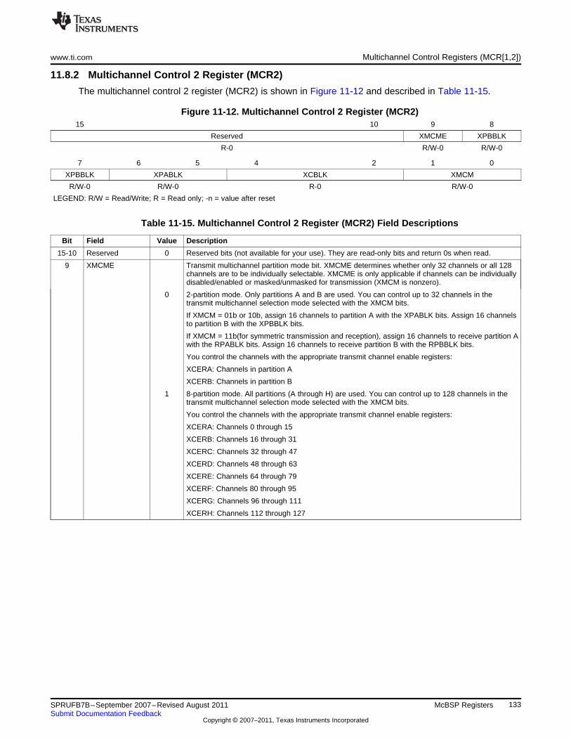
www.ti.com Multichannel Control Registers (MCR[1,2])
11.8.2 Multichannel Control 2 Register (MCR2)
The multichannel control 2 register (MCR2) is shown in Figure 11-12 and described in Table 11-15.
Figure 11-12. Multichannel Control 2 Register (MCR2)15 10 9 8
Reserved XMCME XPBBLK
R-0 R/W-0 R/W-0
7 6 5 4 2 1 0
XPBBLK XPABLK XCBLK XMCM
R/W-0 R/W-0 R-0 R/W-0
LEGEND: R/W = Read/Write; R = Read only; -n = value after reset
Table 11-15. Multichannel Control 2 Register (MCR2) Field Descriptions
Bit Field Value Description
15-10 Reserved 0 Reserved bits (not available for your use). They are read-only bits and return 0s when read.
9 XMCME Transmit multichannel partition mode bit. XMCME determines whether only 32 channels or all 128channels are to be individually selectable. XMCME is only applicable if channels can be individuallydisabled/enabled or masked/unmasked for transmission (XMCM is nonzero).
0 2-partition mode. Only partitions A and B are used. You can control up to 32 channels in thetransmit multichannel selection mode selected with the XMCM bits.
If XMCM = 01b or 10b, assign 16 channels to partition A with the XPABLK bits. Assign 16 channelsto partition B with the XPBBLK bits.
If XMCM = 11b(for symmetric transmission and reception), assign 16 channels to receive partition Awith the RPABLK bits. Assign 16 channels to receive partition B with the RPBBLK bits.
You control the channels with the appropriate transmit channel enable registers:
XCERA: Channels in partition A
XCERB: Channels in partition B
1 8-partition mode. All partitions (A through H) are used. You can control up to 128 channels in thetransmit multichannel selection mode selected with the XMCM bits.
You control the channels with the appropriate transmit channel enable registers:
XCERA: Channels 0 through 15
XCERB: Channels 16 through 31
XCERC: Channels 32 through 47
XCERD: Channels 48 through 63
XCERE: Channels 64 through 79
XCERF: Channels 80 through 95
XCERG: Channels 96 through 111
XCERH: Channels 112 through 127
133SPRUFB7B–September 2007–Revised August 2011 McBSP RegistersSubmit Documentation Feedback
Copyright © 2007–2011, Texas Instruments Incorporated
Multichannel Control Registers (MCR[1,2]) www.ti.com
Table 11-15. Multichannel Control 2 Register (MCR2) Field Descriptions (continued)
Bit Field Value Description
8-7 XPBBLK 0-3h Transmit partition B block bits
XPBBLK is only applicable if channels can be individually disabled/enabled and masked/unmasked(XMCM is nonzero) and the 2-partition mode is selected (XMCME = 0). Under these conditions, theMcBSP transmitter can transmit or withhold data in any of the 32 channels that are assigned topartitions A and B of the transmitter.
The 128 transmit channels of the McBSP are divided equally among 8 blocks (0 through 7). WhenXPBBLK is applicable, use XPBBLK to assign one of the odd-numbered blocks (1, 3, 5, or 7) topartition B, as shown in the following table. Use the XPABLK bit to assign one of theeven-numbered blocks (0, 2, 4, or 6) to partition A.
If you want to use more than 32 channels, you can change block assignments dynamically. Youcan assign a new block to one partition while the transmitter is handling activity in the otherpartition. For example, while the block in partition A is active, you can change which block isassigned to partition B. The XCBLK bits are regularly updated to indicate which block is active.
When XMCM = 11b (for symmetric transmission and reception), the transmitter uses the receiveblock bits (RPABLK and RPBBLK) rather than the transmit block bits (XPABLK and XPBBLK).
0 Block 1: channels 16 through 31
1h Block 3: channels 48 through 63
2h Block 5: channels 80 through 95
3h Block 7: channels 112 through 127
6-5 XPABLK Transmit partition A block bits. XPABLK is only applicable if channels can be individuallydisabled/enabled and masked/unmasked (XMCM is nonzero) and the 2-partition mode is selected(XMCME = 0). Under these conditions, the McBSP transmitter can transmit or withhold data in anyof the 32 channels that are assigned to partitions A and B of the transmitter. See the description forXPBBLK (bits 8-7) for more information about assigning blocks to partitions A and B.
0 Block 0: channels 0 through 15
1h Block 2: channels 32 through 47
2h Block 4: channels 64 through 79
3h Block 6: channels 96 through 111
4-2 XCBLK Transmit current block indicator. XCBLK indicates which block of 16 channels is involved in thecurrent McBSP transmission:
0 Block 0: channels 0 through 15
1h Block 1: channels 16 through 31
2h Block 2: channels 32 through 47
3h Block 3: channels 48 through 63
4h Block 4: channels 64 through 79
5h Block 5: channels 80 through 95
6h Block 6: channels 96 through 111
7h Block 7: channels 112 through 127
1-0 XMCM 0-3h Transmit multichannel selection mode bits. XMCM determines whether all channels or only selectedchannels are enabled and unmasked for transmission. For more details on how the channels areaffected, see Section 5.7 Transmit Multichannel Selection Modes.
0 No transmit multichannel selection mode is on. All channels are enabled and unmasked. Nochannels can be disabled or masked.
1h All channels are disabled unless they are selected in the appropriate transmit channel enableregisters (XCERs). If enabled, a channel in this mode is also unmasked.
The XMCME bit determines whether 32 channels or 128 channels are selectable in XCERs.
2h All channels are enabled, but they are masked unless they are selected in the appropriate transmitchannel enable registers (XCERs).
The XMCME bit determines whether 32 channels or 128 channels are selectable in XCERs.
3h This mode is used for symmetric transmission and reception.
All channels are disabled for transmission unless they are enabled for reception in the appropriatereceive channel enable registers (RCERs). Once enabled, they are masked unless they are alsoselected in the appropriate transmit channel enable registers (XCERs).
The XMCME bit determines whether 32 channels or 128 channels are selectable in RCERs andXCERs.
134 McBSP Registers SPRUFB7B–September 2007–Revised August 2011Submit Documentation Feedback
Copyright © 2007–2011, Texas Instruments Incorporated
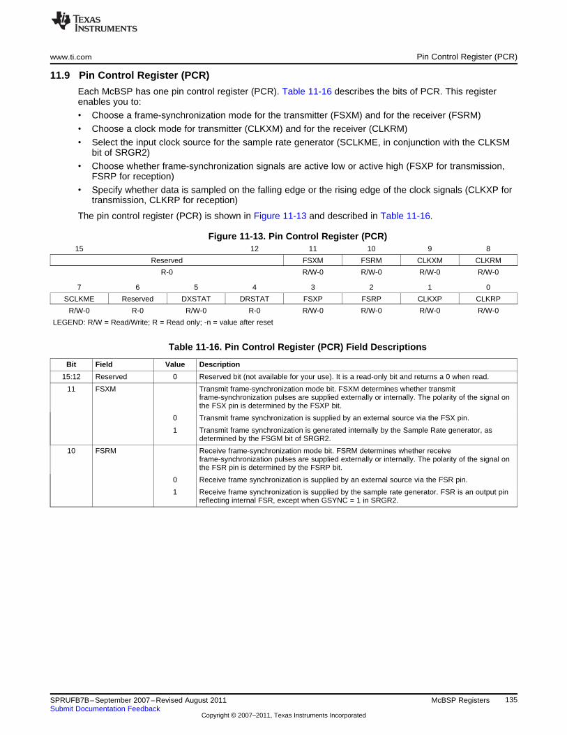
www.ti.com Pin Control Register (PCR)
11.9 Pin Control Register (PCR)
Each McBSP has one pin control register (PCR). Table 11-16 describes the bits of PCR. This registerenables you to:
• Choose a frame-synchronization mode for the transmitter (FSXM) and for the receiver (FSRM)
• Choose a clock mode for transmitter (CLKXM) and for the receiver (CLKRM)
• Select the input clock source for the sample rate generator (SCLKME, in conjunction with the CLKSMbit of SRGR2)
• Choose whether frame-synchronization signals are active low or active high (FSXP for transmission,FSRP for reception)
• Specify whether data is sampled on the falling edge or the rising edge of the clock signals (CLKXP fortransmission, CLKRP for reception)
The pin control register (PCR) is shown in Figure 11-13 and described in Table 11-16.
Figure 11-13. Pin Control Register (PCR)15 12 11 10 9 8
Reserved FSXM FSRM CLKXM CLKRM
R-0 R/W-0 R/W-0 R/W-0 R/W-0
7 6 5 4 3 2 1 0
SCLKME Reserved DXSTAT DRSTAT FSXP FSRP CLKXP CLKRP
R/W-0 R-0 R/W-0 R-0 R/W-0 R/W-0 R/W-0 R/W-0
LEGEND: R/W = Read/Write; R = Read only; -n = value after reset
Table 11-16. Pin Control Register (PCR) Field Descriptions
Bit Field Value Description
15:12 Reserved 0 Reserved bit (not available for your use). It is a read-only bit and returns a 0 when read.
11 FSXM Transmit frame-synchronization mode bit. FSXM determines whether transmitframe-synchronization pulses are supplied externally or internally. The polarity of the signal onthe FSX pin is determined by the FSXP bit.
0 Transmit frame synchronization is supplied by an external source via the FSX pin.
1 Transmit frame synchronization is generated internally by the Sample Rate generator, asdetermined by the FSGM bit of SRGR2.
10 FSRM Receive frame-synchronization mode bit. FSRM determines whether receiveframe-synchronization pulses are supplied externally or internally. The polarity of the signal onthe FSR pin is determined by the FSRP bit.
0 Receive frame synchronization is supplied by an external source via the FSR pin.
1 Receive frame synchronization is supplied by the sample rate generator. FSR is an output pinreflecting internal FSR, except when GSYNC = 1 in SRGR2.
135SPRUFB7B–September 2007–Revised August 2011 McBSP RegistersSubmit Documentation Feedback
Copyright © 2007–2011, Texas Instruments Incorporated
Pin Control Register (PCR) www.ti.com
Table 11-16. Pin Control Register (PCR) Field Descriptions (continued)
Bit Field Value Description
9 CLKXM Transmit clock mode bit. CLKXM determines whether the source for the transmit clock isexternal or internal, and whether the MCLKX pin is an input or an output. The polarity of thesignal on the MCLKX pin is determined by the CLKXP bit.
In the clock stop mode (CLKSTP = 10b or 11b), the McBSP can act as a master or as a slavein the SPI protocol. If the McBSP is a master, make sure that CLKX is an output. If the McBSPis a slave, make sure that CLKX is an input.
Not in clock stop mode (CLKSTP = 00b or 01b):
0 The transmitter gets its clock signal from an external source via the MCLKX pin.
1 Internal CLKX is driven by the sample rate generator of the McBSP. The MCLKX pin is anoutput pin that reflects internal CLKX.
In clock stop mode (CLKSTP = 10b or 11b):
0 The McBSP is a slave in the SPI protocol. The internal transmit clock (CLKX) is driven by theSPI master via the MCLKX pin. The internal receive clock (MCLKR) is driven internally byCLKX, so that both the transmitter and the receiver are controlled by the external master clock.
1 The McBSP is a master in the SPI protocol. The sample rate generator drives the internaltransmit clock (CLKX). Internal CLKX is reflected on the MCLKX pin to drive the shift clock ofthe SPI-compliant slaves in the system. Internal CLKX also drives the internal receive clock(MCLKR), so that both the transmitter and the receiver are controlled by the internal masterclock.
8 CLKRM Receive clock mode bit. The role of CLKRM and the resulting effect on the MCLKR pin dependon whether the McBSP is in the digital loopback mode (DLB = 1).
The polarity of the signal on the MCLKR pin is determined by the CLKRP bit.
Not in digital loopback mode (DLB = 0):
0 The MCLKR pin is an input pin that supplies the internal receive clock (MCLKR).
1 Internal MCLKR is driven by the sample rate generator of the McBSP. The MCLKR pin is anoutput pin that reflects internal MCLKR.
In digital loopback mode (DLB = 1):
0 The MCLKR pin is in the high impedance state. The internal receive clock (MCLKR) is drivenby the internal transmit clock (CLKX). CLKX is derived according to the CLKXM bit.
1 Internal MCLKR is driven by internal CLKX. The MCLKR pin is an output pin that reflectsinternal MCLKR. CLKX is derived according to the CLKXM bit.
7 SCLKME Sample rate generator input clock mode bit. The sample rate generator can produce a clocksignal, CLKG. The frequency of CLKG is:
CLKG freq. = (Input clock frequency) / (CLKGDV + 1)
SCLKME is used in conjunction with the CLKSM bit to select the input clock.
SCLKME CLKSM Input Clock ForSample Rate Generator
0 0 Reserved
0 1 LSPCLK
The input clock for the sample rate generator is taken from the MCLKR pin or from the MCLKXpin, depending on the value of the CLKSM bit of SRGR2:
SCLKME CLKSM Input Clock ForSample Rate Generator
1 0 Signal on MCLKR pin
1 1 Signal on MCLKX pin
6 Reseved
5 DXSTAT DX pin bit. When DXSTAT is applicable, you can toggle the signal on DX by writing toDXSTAT.
DXSTAT is only applicable when the transmitter is in reset (XRST = 0) and DX is configured foruse as a general-purpose output pin.
0 Drive the signal on the DX pin low.
1 Drive the signal on the DX pin high.
136 McBSP Registers SPRUFB7B–September 2007–Revised August 2011Submit Documentation Feedback
Copyright © 2007–2011, Texas Instruments Incorporated
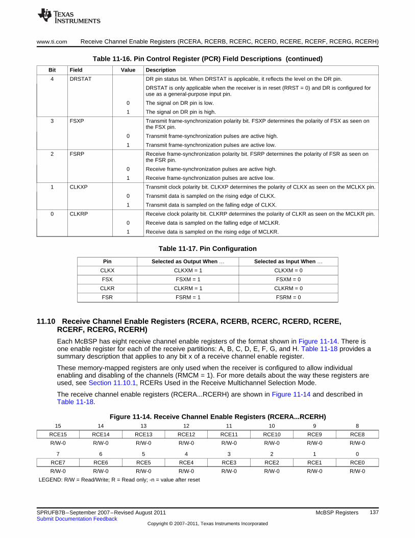
www.ti.com Receive Channel Enable Registers (RCERA, RCERB, RCERC, RCERD, RCERE, RCERF, RCERG, RCERH)
Table 11-16. Pin Control Register (PCR) Field Descriptions (continued)
Bit Field Value Description
4 DRSTAT DR pin status bit. When DRSTAT is applicable, it reflects the level on the DR pin.
DRSTAT is only applicable when the receiver is in reset (RRST = 0) and DR is configured foruse as a general-purpose input pin.
0 The signal on DR pin is low.
1 The signal on DR pin is high.
3 FSXP Transmit frame-synchronization polarity bit. FSXP determines the polarity of FSX as seen onthe FSX pin.
0 Transmit frame-synchronization pulses are active high.
1 Transmit frame-synchronization pulses are active low.
2 FSRP Receive frame-synchronization polarity bit. FSRP determines the polarity of FSR as seen onthe FSR pin.
0 Receive frame-synchronization pulses are active high.
1 Receive frame-synchronization pulses are active low.
1 CLKXP Transmit clock polarity bit. CLKXP determines the polarity of CLKX as seen on the MCLKX pin.
0 Transmit data is sampled on the rising edge of CLKX.
1 Transmit data is sampled on the falling edge of CLKX.
0 CLKRP Receive clock polarity bit. CLKRP determines the polarity of CLKR as seen on the MCLKR pin.
0 Receive data is sampled on the falling edge of MCLKR.
1 Receive data is sampled on the rising edge of MCLKR.
Table 11-17. Pin Configuration
Pin Selected as Output When … Selected as Input When …CLKX CLKXM = 1 CLKXM = 0
FSX FSXM = 1 FSXM = 0
CLKR CLKRM = 1 CLKRM = 0
FSR FSRM = 1 FSRM = 0
11.10 Receive Channel Enable Registers (RCERA, RCERB, RCERC, RCERD, RCERE,RCERF, RCERG, RCERH)
Each McBSP has eight receive channel enable registers of the format shown in Figure 11-14. There isone enable register for each of the receive partitions: A, B, C, D, E, F, G, and H. Table 11-18 provides asummary description that applies to any bit x of a receive channel enable register.
These memory-mapped registers are only used when the receiver is configured to allow individualenabling and disabling of the channels (RMCM = 1). For more details about the way these registers areused, see Section 11.10.1, RCERs Used in the Receive Multichannel Selection Mode.
The receive channel enable registers (RCERA...RCERH) are shown in Figure 11-14 and described inTable 11-18.
Figure 11-14. Receive Channel Enable Registers (RCERA...RCERH)15 14 13 12 11 10 9 8
RCE15 RCE14 RCE13 RCE12 RCE11 RCE10 RCE9 RCE8
R/W-0 R/W-0 R/W-0 R/W-0 R/W-0 R/W-0 R/W-0 R/W-0
7 6 5 4 3 2 1 0
RCE7 RCE6 RCE5 RCE4 RCE3 RCE2 RCE1 RCE0
R/W-0 R/W-0 R/W-0 R/W-0 R/W-0 R/W-0 R/W-0 R/W-0
LEGEND: R/W = Read/Write; R = Read only; -n = value after reset
137SPRUFB7B–September 2007–Revised August 2011 McBSP RegistersSubmit Documentation Feedback
Copyright © 2007–2011, Texas Instruments Incorporated
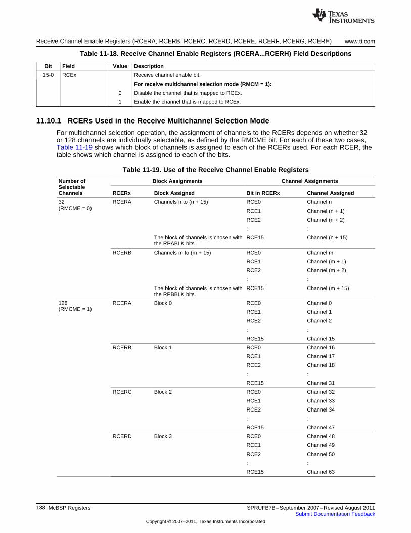
Receive Channel Enable Registers (RCERA, RCERB, RCERC, RCERD, RCERE, RCERF, RCERG, RCERH) www.ti.com
Table 11-18. Receive Channel Enable Registers (RCERA...RCERH) Field Descriptions
Bit Field Value Description
15-0 RCEx Receive channel enable bit.
For receive multichannel selection mode (RMCM = 1):
0 Disable the channel that is mapped to RCEx.
1 Enable the channel that is mapped to RCEx.
11.10.1 RCERs Used in the Receive Multichannel Selection Mode
For multichannel selection operation, the assignment of channels to the RCERs depends on whether 32or 128 channels are individually selectable, as defined by the RMCME bit. For each of these two cases,Table 11-19 shows which block of channels is assigned to each of the RCERs used. For each RCER, thetable shows which channel is assigned to each of the bits.
Table 11-19. Use of the Receive Channel Enable Registers
Number of Block Assignments Channel AssignmentsSelectableChannels RCERx Block Assigned Bit in RCERx Channel Assigned
32 RCERA Channels n to (n + 15) RCE0 Channel n(RMCME = 0) RCE1 Channel (n + 1)
RCE2 Channel (n + 2)
: :
The block of channels is chosen with RCE15 Channel (n + 15)the RPABLK bits.
RCERB Channels m to (m + 15) RCE0 Channel m
RCE1 Channel (m + 1)
RCE2 Channel (m + 2)
: :
The block of channels is chosen with RCE15 Channel (m + 15)the RPBBLK bits.
128 RCERA Block 0 RCE0 Channel 0(RMCME = 1) RCE1 Channel 1
RCE2 Channel 2
: :
RCE15 Channel 15
RCERB Block 1 RCE0 Channel 16
RCE1 Channel 17
RCE2 Channel 18
: :
RCE15 Channel 31
RCERC Block 2 RCE0 Channel 32
RCE1 Channel 33
RCE2 Channel 34
: :
RCE15 Channel 47
RCERD Block 3 RCE0 Channel 48
RCE1 Channel 49
RCE2 Channel 50
: :
RCE15 Channel 63
138 McBSP Registers SPRUFB7B–September 2007–Revised August 2011Submit Documentation Feedback
Copyright © 2007–2011, Texas Instruments Incorporated
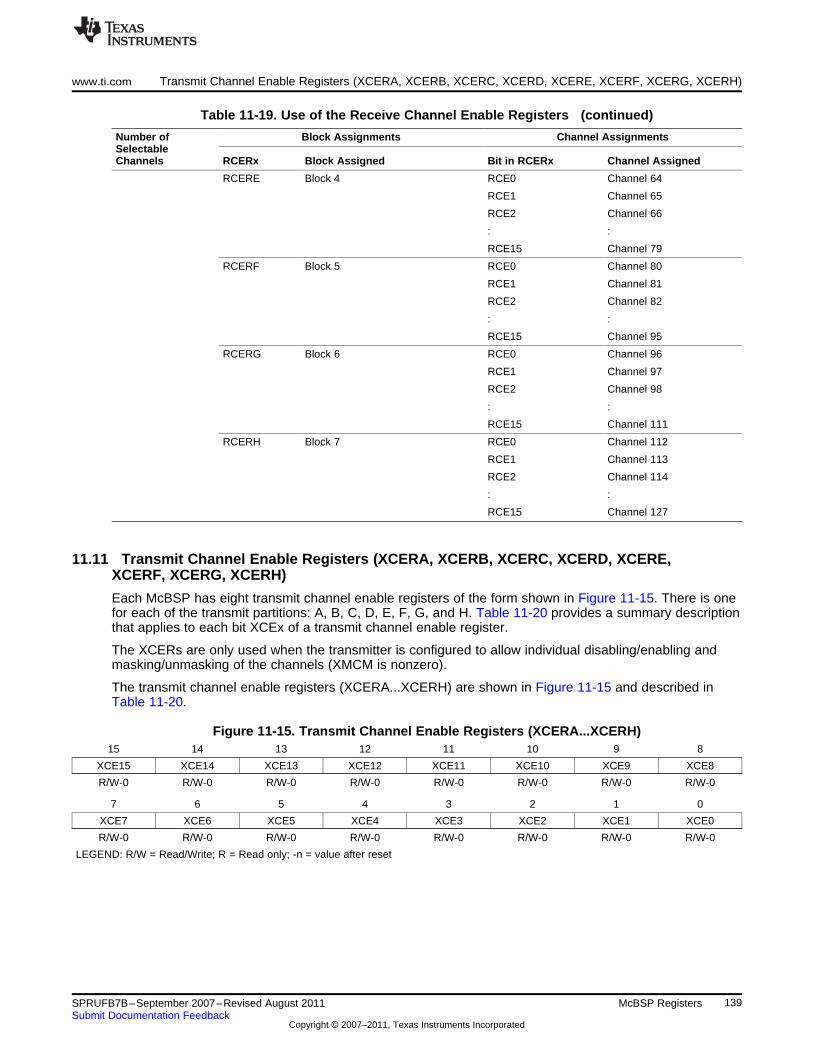
www.ti.com Transmit Channel Enable Registers (XCERA, XCERB, XCERC, XCERD, XCERE, XCERF, XCERG, XCERH)
Table 11-19. Use of the Receive Channel Enable Registers (continued)
Number of Block Assignments Channel AssignmentsSelectableChannels RCERx Block Assigned Bit in RCERx Channel Assigned
RCERE Block 4 RCE0 Channel 64
RCE1 Channel 65
RCE2 Channel 66
: :
RCE15 Channel 79
RCERF Block 5 RCE0 Channel 80
RCE1 Channel 81
RCE2 Channel 82
: :
RCE15 Channel 95
RCERG Block 6 RCE0 Channel 96
RCE1 Channel 97
RCE2 Channel 98
: :
RCE15 Channel 111
RCERH Block 7 RCE0 Channel 112
RCE1 Channel 113
RCE2 Channel 114
: :
RCE15 Channel 127
11.11 Transmit Channel Enable Registers (XCERA, XCERB, XCERC, XCERD, XCERE,XCERF, XCERG, XCERH)
Each McBSP has eight transmit channel enable registers of the form shown in Figure 11-15. There is onefor each of the transmit partitions: A, B, C, D, E, F, G, and H. Table 11-20 provides a summary descriptionthat applies to each bit XCEx of a transmit channel enable register.
The XCERs are only used when the transmitter is configured to allow individual disabling/enabling andmasking/unmasking of the channels (XMCM is nonzero).
The transmit channel enable registers (XCERA...XCERH) are shown in Figure 11-15 and described inTable 11-20.
Figure 11-15. Transmit Channel Enable Registers (XCERA...XCERH)15 14 13 12 11 10 9 8
XCE15 XCE14 XCE13 XCE12 XCE11 XCE10 XCE9 XCE8
R/W-0 R/W-0 R/W-0 R/W-0 R/W-0 R/W-0 R/W-0 R/W-0
7 6 5 4 3 2 1 0
XCE7 XCE6 XCE5 XCE4 XCE3 XCE2 XCE1 XCE0
R/W-0 R/W-0 R/W-0 R/W-0 R/W-0 R/W-0 R/W-0 R/W-0
LEGEND: R/W = Read/Write; R = Read only; -n = value after reset
139SPRUFB7B–September 2007–Revised August 2011 McBSP RegistersSubmit Documentation Feedback
Copyright © 2007–2011, Texas Instruments Incorporated
Transmit Channel Enable Registers (XCERA, XCERB, XCERC, XCERD, XCERE, XCERF, XCERG, XCERH) www.ti.com
Table 11-20. Transmit Channel Enable Registers (XCERA...XCERH) Field Descriptions
Bit Field Value Description
15-0 XCEx Transmit channel enable bit. The role of this bit depends on which transmit multichannel selectionmode is selected with the XMCM bits.
For multichannel selection when XMCM = 01b(all channels disabled unless selected):
0 Disable and mask the channel that is mapped to XCEx.
1 Enable and unmask the channel that is mapped to XCEx.
For multichannel selection when XMCM = 10b(all channels enabled but masked unless selected):
0 Mask the channel that is mapped to XCEx.
1 Unmask the channel that is mapped to XCEx.
For multichannel selection when XMCM = 11b(all channels masked unless selected):
0 Mask the channel that is mapped to XCEx. Even if the channel is enabled by the correspondingreceive channel enable bit, this channel's data cannot appear on the DX pin.
1 Unmask the channel that is mapped to XCEx. If the channel is also enabled by the correspondingreceive channel enable bit, full transmission can occur.
11.11.1 XCERs Used in a Transmit Multichannel Selection Mode
For multichannel selection operation, the assignment of channels to the XCERs depends on whether 32 or128 channels are individually selectable, as defined by the XMCME bit. These two cases are shown inTable 11-21. The table shows which block of channels is assigned to each XCER that is used. For eachXCER, the table shows which channel is assigned to each of the bits.
NOTE: When XMCM = 11b (for symmetric transmission and reception), the transmitter uses thereceive channel enable registers (RCERs) to enable channels and uses the XCERs tounmask channels for transmission.
Table 11-21. Use of the Transmit Channel Enable Registers
Number of Block Assignments Channel AssignmentsSelectableChannels XCERx Block Assigned Bit in XCERx Channel Assigned
32 XCERA Channels n to (n + 15) XCE0 Channel n(XMCME = 0) XCE1 Channel (n + 1)
XCE2 Channel (n + 2)
: :
When XMCM = 01b or 10b, the block XCE15 Channel (n + 15)of channels is chosen with theXPABLK bits. When XMCM = 11b,the block is chosen with the RPABLKbits.
XCERB Channels m to (m + 15) XCE0 Channel m
XCE1 Channel (m + 1)
XCE2 Channel (m + 2)
: :
When XMCM = 01b or 10b, the block XCE15 Channel (m + 15)of channels is chosen with theXPBBLK bits. When XMCM = 11b,the block is chosen with the RPBBLKbits.
140 McBSP Registers SPRUFB7B–September 2007–Revised August 2011Submit Documentation Feedback
Copyright © 2007–2011, Texas Instruments Incorporated
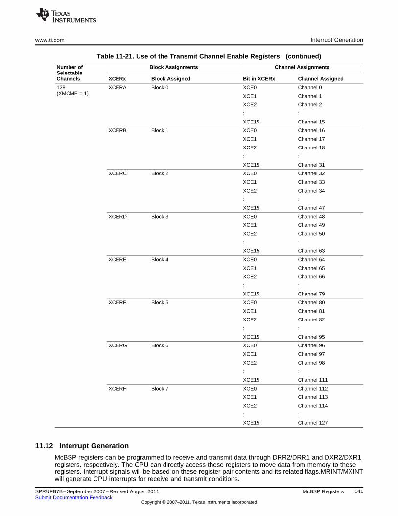
www.ti.com Interrupt Generation
Table 11-21. Use of the Transmit Channel Enable Registers (continued)
Number of Block Assignments Channel AssignmentsSelectableChannels XCERx Block Assigned Bit in XCERx Channel Assigned
128 XCERA Block 0 XCE0 Channel 0(XMCME = 1) XCE1 Channel 1
XCE2 Channel 2
: :
XCE15 Channel 15
XCERB Block 1 XCE0 Channel 16
XCE1 Channel 17
XCE2 Channel 18
: :
XCE15 Channel 31
XCERC Block 2 XCE0 Channel 32
XCE1 Channel 33
XCE2 Channel 34
: :
XCE15 Channel 47
XCERD Block 3 XCE0 Channel 48
XCE1 Channel 49
XCE2 Channel 50
: :
XCE15 Channel 63
XCERE Block 4 XCE0 Channel 64
XCE1 Channel 65
XCE2 Channel 66
: :
XCE15 Channel 79
XCERF Block 5 XCE0 Channel 80
XCE1 Channel 81
XCE2 Channel 82
: :
XCE15 Channel 95
XCERG Block 6 XCE0 Channel 96
XCE1 Channel 97
XCE2 Channel 98
: :
XCE15 Channel 111
XCERH Block 7 XCE0 Channel 112
XCE1 Channel 113
XCE2 Channel 114
: :
XCE15 Channel 127
11.12 Interrupt Generation
McBSP registers can be programmed to receive and transmit data through DRR2/DRR1 and DXR2/DXR1registers, respectively. The CPU can directly access these registers to move data from memory to theseregisters. Interrupt signals will be based on these register pair contents and its related flags.MRINT/MXINTwill generate CPU interrupts for receive and transmit conditions.
141SPRUFB7B–September 2007–Revised August 2011 McBSP RegistersSubmit Documentation Feedback
Copyright © 2007–2011, Texas Instruments Incorporated
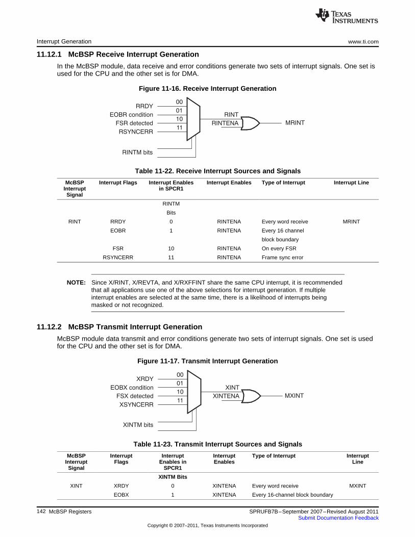
RRDY00
EOBR condition01
FSR detected10
RSYNCERR11
RINTM bits
RINT
RINTENA MRINT
XRDY00
EOBX condition01
FSX detected10
XSYNCERR11
XINTM bits
XINT
XINTENA MXINT
Interrupt Generation www.ti.com
11.12.1 McBSP Receive Interrupt Generation
In the McBSP module, data receive and error conditions generate two sets of interrupt signals. One set isused for the CPU and the other set is for DMA.
Figure 11-16. Receive Interrupt Generation
Table 11-22. Receive Interrupt Sources and Signals
McBSP Interrupt Flags Interrupt Enables Interrupt Enables Type of Interrupt Interrupt LineInterrupt in SPCR1Signal
RINTM
Bits
RINT RRDY 0 RINTENA Every word receive MRINT
EOBR 1 RINTENA Every 16 channel
block boundary
FSR 10 RINTENA On every FSR
RSYNCERR 11 RINTENA Frame sync error
NOTE: Since X/RINT, X/REVTA, and X/RXFFINT share the same CPU interrupt, it is recommendedthat all applications use one of the above selections for interrupt generation. If multipleinterrupt enables are selected at the same time, there is a likelihood of interrupts beingmasked or not recognized.
11.12.2 McBSP Transmit Interrupt Generation
McBSP module data transmit and error conditions generate two sets of interrupt signals. One set is usedfor the CPU and the other set is for DMA.
Figure 11-17. Transmit Interrupt Generation
Table 11-23. Transmit Interrupt Sources and Signals
McBSP Interrupt Interrupt Interrupt Type of Interrupt InterruptInterrupt Flags Enables in Enables Line
Signal SPCR1
XINTM Bits
XINT XRDY 0 XINTENA Every word receive MXINT
EOBX 1 XINTENA Every 16-channel block boundary
142 McBSP Registers SPRUFB7B–September 2007–Revised August 2011Submit Documentation Feedback
Copyright © 2007–2011, Texas Instruments Incorporated
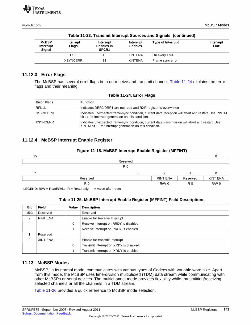
www.ti.com McBSP Modes
Table 11-23. Transmit Interrupt Sources and Signals (continued)
McBSP Interrupt Interrupt Interrupt Type of Interrupt InterruptInterrupt Flags Enables in Enables Line
Signal SPCR1
FSX 10 XINTENA On every FSX
XSYNCERR 11 XINTENA Frame sync error
11.12.3 Error Flags
The McBSP has several error flags both on receive and transmit channel. Table 11-24 explains the errorflags and their meaning.
Table 11-24. Error Flags
Error Flags Function
RFULL Indicates DRR2/DRR1 are not read and RXR register is overwritten
RSYNCERR Indicates unexpected frame-sync condition, current data reception will abort and restart. Use RINTMbit 11 for interrupt generation on this condition.
XSYNCERR Indicates unexpected frame-sync condition, current data transmission will abort and restart. UseXINTM bit 11 for interrupt generation on this condition.
11.12.4 McBSP Interrupt Enable Register
Figure 11-18. McBSP Interrupt Enable Register (MFFINT)15 8
Reserved
R-0
7 3 2 1 0
Reserved RINT ENA Reserved XINT ENA
R-0 R/W-0 R-0 R/W-0
LEGEND: R/W = Read/Write; R = Read only; -n = value after reset
Table 11-25. McBSP Interrupt Enable Register (MFFINT) Field Descriptions
Bit Field Value Description
15:3 Reserved Reserved
2 RINT ENA Enable for Receive Interrupt
0 Receive interrupt on RRDY is disabled.
1 Receive interrupt on RRDY is enabled.
1 Reserved
0 XINT ENA Enable for transmit Interrupt
0 Transmit interrupt on XRDY is disabled.
1 Transmit interrupt on XRDY is enabled.
11.13 McBSP Modes
McBSP, in its normal mode, communicates with various types of Codecs with variable word size. Apartfrom this mode, the McBSP uses time-division multiplexed (TDM) data stream while communicating withother McBSPs or serial devices. The multichannel mode provides flexibility while transmitting/receivingselected channels or all the channels in a TDM stream.
Table 11-26 provides a quick reference to McBSP mode selection.
143SPRUFB7B–September 2007–Revised August 2011 McBSP RegistersSubmit Documentation Feedback
Copyright © 2007–2011, Texas Instruments Incorporated
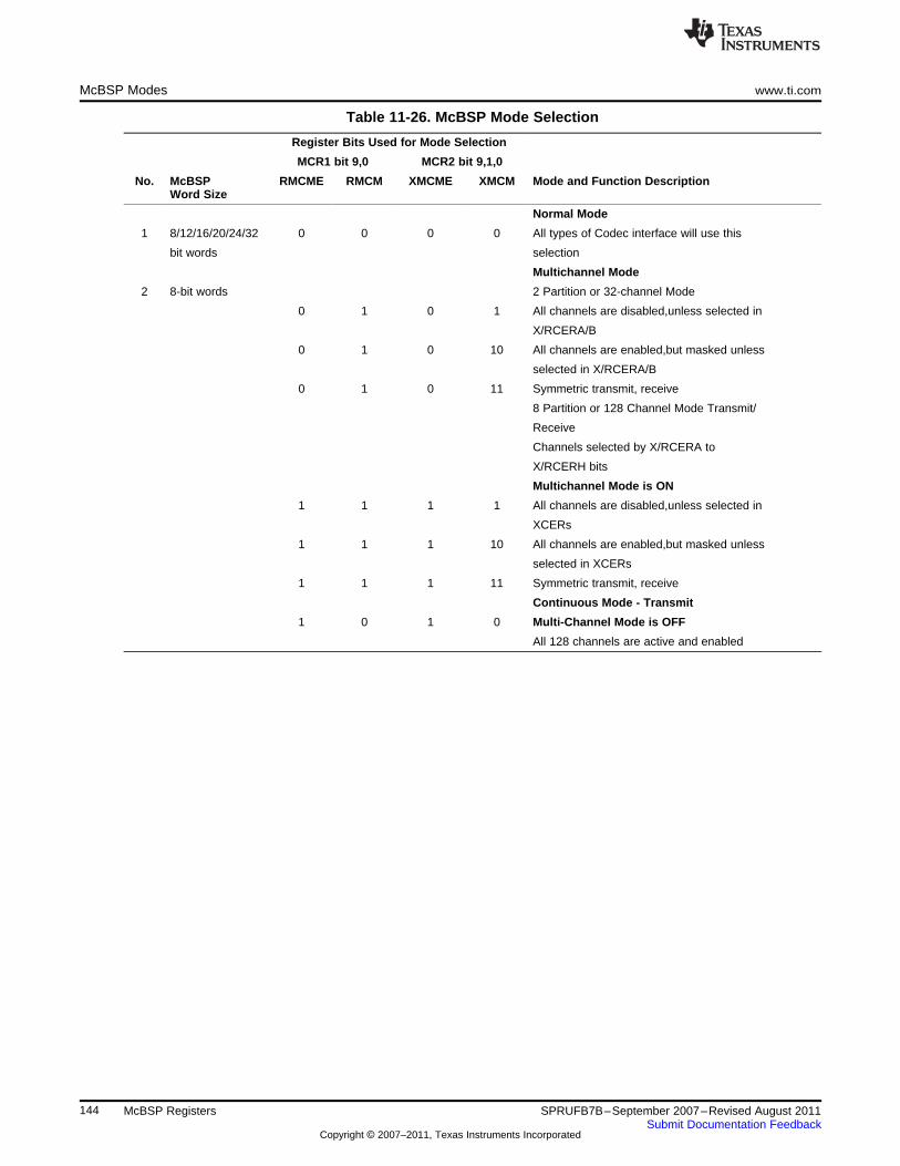
McBSP Modes www.ti.com
Table 11-26. McBSP Mode Selection
Register Bits Used for Mode Selection
MCR1 bit 9,0 MCR2 bit 9,1,0
No. McBSP RMCME RMCM XMCME XMCM Mode and Function DescriptionWord Size
Normal Mode
1 8/12/16/20/24/32 0 0 0 0 All types of Codec interface will use this
bit words selection
Multichannel Mode
2 8-bit words 2 Partition or 32-channel Mode
0 1 0 1 All channels are disabled,unless selected in
X/RCERA/B
0 1 0 10 All channels are enabled,but masked unless
selected in X/RCERA/B
0 1 0 11 Symmetric transmit, receive
8 Partition or 128 Channel Mode Transmit/
Receive
Channels selected by X/RCERA to
X/RCERH bits
Multichannel Mode is ON
1 1 1 1 All channels are disabled,unless selected in
XCERs
1 1 1 10 All channels are enabled,but masked unless
selected in XCERs
1 1 1 11 Symmetric transmit, receive
Continuous Mode - Transmit
1 0 1 0 Multi-Channel Mode is OFF
All 128 channels are active and enabled
144 McBSP Registers SPRUFB7B–September 2007–Revised August 2011Submit Documentation Feedback
Copyright © 2007–2011, Texas Instruments Incorporated
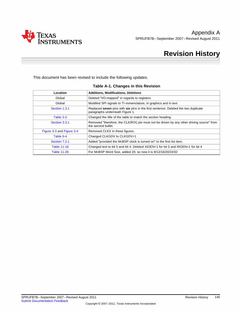
Appendix ASPRUFB7B–September 2007–Revised August 2011
Revision History
This document has been revised to include the following updates.
Table A-1. Changes in this Revision
Location Additions, Modifications, Deletions
Global Deleted "I/O-mapped" in regards to registers
Global Modified SPI signals to TI nomenclature, in graphics and in text
Section 1.3.1 Replaced seven pins with six pins in the first sentence. Deleted the two duplicateparagraphs underneath Figure 1.
Table 2-2 Changed the title of the table to match the section heading.
Section 3.3.1 Removed "therefore, the CLK(R/X) pin must not be driven by any other driving source" fromthe second bullet.
Figure 3-3 and Figure 3-4 Removed CLKX in these figures.
Table 6-4 Changed CLKGDV to CLKGDV=1
Section 7.2.1 Added "provided the McBSP clock is turned on" to the first list item.
Table 11-16 Changed text to bit 5 and bit 4. Deleted XIOEN=1 for bit 5 and RIOEN=1 for bit 4
Table 11-26 For McBSP Word Size, added 20; so now it is 8/12/16/20/24/32
145SPRUFB7B–September 2007–Revised August 2011 Revision HistorySubmit Documentation Feedback
Copyright © 2007–2011, Texas Instruments Incorporated

IMPORTANT NOTICE
Texas Instruments Incorporated and its subsidiaries (TI) reserve the right to make corrections, modifications, enhancements, improvements,and other changes to its products and services at any time and to discontinue any product or service without notice. Customers shouldobtain the latest relevant information before placing orders and should verify that such information is current and complete. All products aresold subject to TI’s terms and conditions of sale supplied at the time of order acknowledgment.
TI warrants performance of its hardware products to the specifications applicable at the time of sale in accordance with TI’s standardwarranty. Testing and other quality control techniques are used to the extent TI deems necessary to support this warranty. Except wheremandated by government requirements, testing of all parameters of each product is not necessarily performed.
TI assumes no liability for applications assistance or customer product design. Customers are responsible for their products andapplications using TI components. To minimize the risks associated with customer products and applications, customers should provideadequate design and operating safeguards.
TI does not warrant or represent that any license, either express or implied, is granted under any TI patent right, copyright, mask work right,or other TI intellectual property right relating to any combination, machine, or process in which TI products or services are used. Informationpublished by TI regarding third-party products or services does not constitute a license from TI to use such products or services or awarranty or endorsement thereof. Use of such information may require a license from a third party under the patents or other intellectualproperty of the third party, or a license from TI under the patents or other intellectual property of TI.
Reproduction of TI information in TI data books or data sheets is permissible only if reproduction is without alteration and is accompaniedby all associated warranties, conditions, limitations, and notices. Reproduction of this information with alteration is an unfair and deceptivebusiness practice. TI is not responsible or liable for such altered documentation. Information of third parties may be subject to additionalrestrictions.
Resale of TI products or services with statements different from or beyond the parameters stated by TI for that product or service voids allexpress and any implied warranties for the associated TI product or service and is an unfair and deceptive business practice. TI is notresponsible or liable for any such statements.
TI products are not authorized for use in safety-critical applications (such as life support) where a failure of the TI product would reasonablybe expected to cause severe personal injury or death, unless officers of the parties have executed an agreement specifically governingsuch use. Buyers represent that they have all necessary expertise in the safety and regulatory ramifications of their applications, andacknowledge and agree that they are solely responsible for all legal, regulatory and safety-related requirements concerning their productsand any use of TI products in such safety-critical applications, notwithstanding any applications-related information or support that may beprovided by TI. Further, Buyers must fully indemnify TI and its representatives against any damages arising out of the use of TI products insuch safety-critical applications.
TI products are neither designed nor intended for use in military/aerospace applications or environments unless the TI products arespecifically designated by TI as military-grade or "enhanced plastic." Only products designated by TI as military-grade meet militaryspecifications. Buyers acknowledge and agree that any such use of TI products which TI has not designated as military-grade is solely atthe Buyer's risk, and that they are solely responsible for compliance with all legal and regulatory requirements in connection with such use.
TI products are neither designed nor intended for use in automotive applications or environments unless the specific TI products aredesignated by TI as compliant with ISO/TS 16949 requirements. Buyers acknowledge and agree that, if they use any non-designatedproducts in automotive applications, TI will not be responsible for any failure to meet such requirements.
Following are URLs where you can obtain information on other Texas Instruments products and application solutions:
Products Applications
Audio www.ti.com/audio Communications and Telecom www.ti.com/communications
Amplifiers amplifier.ti.com Computers and Peripherals www.ti.com/computers
Data Converters dataconverter.ti.com Consumer Electronics www.ti.com/consumer-apps
DLP® Products www.dlp.com Energy and Lighting www.ti.com/energy
DSP dsp.ti.com Industrial www.ti.com/industrial
Clocks and Timers www.ti.com/clocks Medical www.ti.com/medical
Interface interface.ti.com Security www.ti.com/security
Logic logic.ti.com Space, Avionics and Defense www.ti.com/space-avionics-defense
Power Mgmt power.ti.com Transportation and Automotive www.ti.com/automotive
Microcontrollers microcontroller.ti.com Video and Imaging www.ti.com/video
RFID www.ti-rfid.com
OMAP Mobile Processors www.ti.com/omap
Wireless Connctivity www.ti.com/wirelessconnectivity
TI E2E Community Home Page e2e.ti.com
Mailing Address: Texas Instruments, Post Office Box 655303, Dallas, Texas 75265Copyright © 2011, Texas Instruments Incorporated