interfacing the adsp-21161 simd sharc dsp to the ad1836 ... · use of serial port...
TRANSCRIPT

a
Interfacing the ADSP-21161 SIMD SHARC DSP to the AD1836 (24-bit/96kHz) Multichannel Codec
Example Interface Drivers in Assembly and C For Use With The 21161 EZ-KIT-LITE
DAC1 DAC2 DAC3 DAC4 DAC5 DAC6
ADC1 ADC2 ADC3 ADC4
Serial / Interface AUX I 2 S Input
text a
S/PDIF Receiver
AUX DAC AUX DAC AD1852
A D 1 8 3 6 AUX I 2 S Output
A D S P -2 1 1 6 1
Version 1.0A
John Tomarakos ADI DSP Applications
9/14/01

Figure 1. 24-bit/96kHz AD1836 Multichannel Audio Codec
0. Introduction This application note describes how to interface the ADSP-21161 to the AD1836 for use in professional, consumer, or automotive audio systems. Using the AD1836 gives the DSP audio system designer more flexibility for capture and playback of "professional-quality" 24-bit audio by providing the capability of processing multiple high-fidelity digital audio signals simultaneously.
The AD1836 Multichannel 24-bit 96kHz Codec is a high-performance, single-chip 5 Volt stereo Codec system providing three stereo DACs and two stereo ADC’s using patented Sigma-delta conversion techniques. The ADCs and DACs are capable of maintaining 105 dB SNR and Dynamic Range. With extended serial port TDM and auxiliary I/O features, the AD1836 can also interfaced to additional external audio I2S devices, providing a "backdoor" path to the TDM bus for 3 external I2S devices, to allow 8-channel I/O. The ability to utilize 8 input/output channels of audio enables the use of the AD1836 in a wide variety of professional and consumer audio applications requiring multiple I/O, such as: digital mixers, effects processors, home recording studios, DVD players, home theatre systems and automotive audio systems. No additional hardware glue-logic is required for the simple TDM interface mode, and the programming of the AD1836 modes of operation is easily accomplished through DSP software programming. Please note that this application note will only describe the AD1836's TDM interface, and not the other modes of operation (I2S, packed mode, etc).
The ADSP-21161 SIMD SHARC DSP offers 2 identical computation unit sets (2 register files, 2 ALUs, 2 MACs, 2 barrel shifters), providing the ability to process multiple 24-bit audio streams concurrently with the use of SIMD. The two computation units can process audio streams with either 32-bit fixed point, 32-bit IEEE floating point, or 40-bit extended precision floating point processing. Thus, the ability to maintain the integrity of the 24-bit/105 dB signal quality is achievable through 32-bit audio processing without resorting to double precision arithmetic, and a 2x performance increase for many standard DSP algorithms, such as FIRs, IIRs, and FFTs.
AD1836 assembly and C driver source code examples are provided in the application note for reference purposes. This source code was tested and verified using the ADDS-21161N EZ-KIT Lite Development Platform, which includes an AD1836, AD1852 and SP/DIF receiver as the analog/digital audio interface.
I would like to also thank Dan Ledger of Analog Devices for his contribution of the AD1836 C-based Driver Source Code!

0.1 ADSP-2161 EZ-KIT Lite: An AD1836/ADSP-21161 Audio System Reference Design The AD1836/ADSP-21161 pairing satisfies the higher fidelity audio requirements for new emerging audio applications, and offers many advantages for a low-cost high-fidelity audio platform, including: • AD1836's TDM Serial Mode enables DSP Serial Port Multichannel Mode (TDM) Compatibility.
This mode enables a protocol where each TDM (time-division multiplexed) frame sync generates 8 timeslots which are 32-bits per slot, allowing a much easier interface to 32-bit DSPs that support a TDM interface. The TDM approach allows the use of serial port 'autobuffering' or 'DMA chaining' along with the ADSP-21xxx Serial Port Multichannel Mode (TDM) operation. The AD1836 TDM interface also allows the DSP system designer to require the use of 1 TDM serial port pair, saving the use of an additional serial port. For example, on the ADSP-21161, 3 SPORTs would be necessary to be able to communicate with the AD1836's 2 stereo I2S ADCs and 3 stereo I2S DACs.
• Sampling Rate support for 24-bit, 48/96 kHz
The AD1836 can generate sample rates of 48 kHz and 96 kHz, enabling the capability to record and play back higher quality audio. Recent studies in human hearing indicate that 16-bit CD-quality audio does not suffice for high-fidelity audio, and at least 24-bit/96kHz processing is required.
• High Quality 105 dB Dynamic Range and Signal to Noise Ratio on the ADCs and DACs
Surpassing the 'CD-Quality' sound offered by 16-bit conversion (96 dB maximum), the ability to maintain 105 dB approaches signal quality typically found only in expensive professional audio systems.
• 32-bit SIMD Fixed Point, or 32/40-bit Floating Point Audio Processing of 24-bit digitized signals at 600 Mflops Peak,
400 Mflops sustained performance The ADSP-21161's SIMD (single-instruction, multiple-data) architecture enables multichannel processing of audio signals simultaneously via 2 identical computation units, providing the ability to maintain the 24-bit signal integrity by ensuring that any quantization errors produced during arithmetic operations are lower than the 105 dB noise floor of the AD1836 ADCs and DACs.
Figure 2. 21161 EZ-KIT Lite / AD1836 Audio Development System

Figure 3. ADDS-21161-EZLITE Development Board Functional Block Diagram
The ADDS-21161N-EZLITE evaluation contains the following components:
ADSP-21161N SHARC DSP running at 100 MHz
Memory 1 M-bit (on-chip memory) 1M x 48 SDRAM running at 100 MHz 512K x 8-bit Flash Memory
Cypress CY7C6403 EZ-USB Microcontroller (16-bit Host) connected to the JTAG port, providing "nonintrusive" JTAG emulator functionality through a
PC's USB port.
AD1836 Codec (24-bit, 96 kHz, 4 ADCs, 6 DACs)
AD1852 Stereo DAC (24-bit, 96 kHz)
Crystal CS8414 24-bit, 96 kHz SP/DIF receiver
1 Stereo Microphone I/P Jack, 1 Line-In RCA I/P Jack, 8 RCA O/P Jacks, Optical/RCA input for digital audio input
EZ-ICE JTAG Emulation Connector
Expansion Connectors (EP, SPORTs, Link Ports)
6 Output LEDs, 4 Input FLAG pushbuttons, 3 IRQ pushbuttons

0.2 The Benefits of 32-bit Audio Processing of 24-bit "professional-quality" audio Today 16-bit, 44.1 kHz PCM digital audio continues to be the standard for high quality audio in most current applications, such as CD, DAT and PC audio. When the compact disc was introduced in the early 1980s, audio designers elected to work with 16-bit words sampled at 44.1 kHz for a mixture of technical and commercial reasons. Factors that limited their options included the quality of available A/Ds, the quality and cost of other digital components, and the density at which available media could store digital data. They also thought that the format would be sufficient to record audio signals with all the fidelity required for the full range of human hearing. But recent technological developments and improved knowledge of human hearing have created a demand for greater word lengths in the professional audio sector. Research within the last decade indicates that the sensitivity of the human ear is such that the dynamic range between the quietest sound the average person can detect and the maximum sound that person can experience without pain is approximately 120 dB. Concerning word width, it’s clear that 16-bit CD-quality audio no longer corresponds to the highest-quality audio a system should be able to store and play back. Digital converter technology has advanced to where audio engineers can make recordings with a dynamic range of 120 dB or greater, but a compact disc is unable to accurately carry them because the CD standard limits word size to 16 bits. Many manufacturers of pro equipment have already developed new products using 24-bit conversion and 96-kHz sample rates. Many recording studios now routinely master their recordings using 20-bit recorders, and are quickly moving to 24 bits. These technological developments are now making their way into the consumer and so-called “prosumer” audio markets. The most evident consumer incarnation is DVD which is capable of carrying audio with up to 24-bit resolution. New DVD standards are extending the digital formats to 24-bits at sample rates of 96 kHz and 192 kHz formats. Other products include DAT recorders which can sample at 96kHz. Many professional audio studio manufacturers now offer DAT recorders with 24-bit conversion, 96 kHz sampling rate. In fact, three trends can be identified which have influenced the current generation of digital audio formats which are set to replace CD digital audio, and these may be summarized as follows: • Higher resolution - 20 or 24 bits per word • Higher sampling frequency - typically 96 kHz • More audio channels The Analog Devices AD1836 offers 24-bit, 96 kHz multichannel audio capability to meet many new requirements in the professional, consumer and automotive audio markets. Multibit sigma-delta converters such as the AD1836 are capable of 24-bit resolution, capable of exceeding the 80 to 96 dB dynamic range available using 16 bit conversion. The popularity of 24-bit D/As is increasing for both professional and high-end consumer applications. The reason for using these higher precision converters for audio processing is clear: their distortion performance (linearity) is far superior than possible with 16-bit converters. The other obvious reason is the increase in SNR and dynamic range. Now consider the DSP word size with respect to the converter's word size for processing digitized audio samples. Figure 4 shows the capable dynamic ranges for DSPs with native data word widths of 16, 24, or 32-bit data (assuming fractional fixed-point data types). Assuming 6 dB per bit, a 16-bit DSP can support dynamic ranges of 96 dB, a 24-bit can support 144 dB, while a 32-bit DSP that has native fixed point support (such as the ADSP-21161) can support signals up to 196 dB. In general, if a digital system produces processing artifacts which are above the noise floor of the input signal, then these artifacts will be audible under certain circumstances, such as when an input signal is of low intensity or limited frequency content. Therefore, the digital processing algorithm operating on the input A/D samples should be designed to prevent processing noise from reaching levels at which it may appear above the converter's noise floor of the input and hence become audible [3]. For a digital filter routine to operate transparently, the resolution of the processing system must be considerably greater than that of the input signal so that any errors introduced by the arithmetic computations are smaller than the precision of the ADCs or DACs. In order for the DSP to maintain the SNR established by the A/D converters, all intermediate DSP calculations require the use of higher precision processing as recommended by Wilson, Dattorro, and Zolzer [3, 4, 5]. Some manifestations of the causes of finite word length effects that can degrade an audio signal’s SNR are: A/D conversion noise, quantization error of arithmetic computations from truncation and rounding, computational overflow and coefficient quantization.
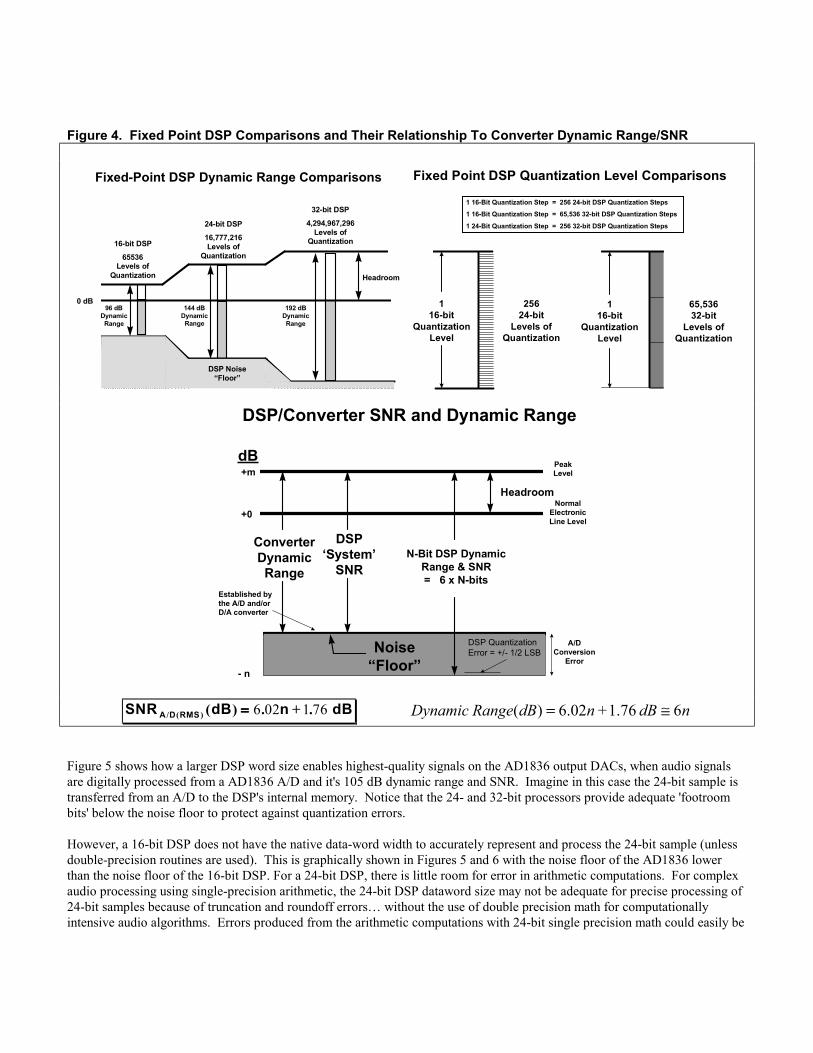
Figure 4. Fixed Point DSP Comparisons and Their Relationship To Converter Dynamic Range/SNR
Fixed-Point DSP Dynamic Range Comparisons
16-bit DSP65536
Levels ofQuantization
32-bit DSP4,294,967,296
Levels ofQuantization
24-bit DSP16,777,216Levels of
Quantization
0 dB96 dB
DynamicRange
144 dBDynamic
Range
192 dBDynamicRange
Headroom
DSP Noise“Floor”
Fixed Point DSP Quantization Level Comparisons
1 16-Bit Quantization Step = 256 24-bit DSP Quantization Steps1 16-Bit Quantization Step = 65,536 32-bit DSP Quantization Steps
1 24-Bit Quantization Step = 256 32-bit DSP Quantization Steps
25624-bit
Levels ofQuantization
116-bit
QuantizationLevel
116-bit
QuantizationLevel
65,53632-bit
Levels ofQuantization
DSP/Converter SNR and Dynamic Range
DSP‘System’
SNR
Headroom
N-Bit DSP DynamicRange & SNR= 6 x N-bits
dB
+0
Noise“Floor”
Established bythe A/D and/orD/A converter
- n
+m
ConverterDynamicRange
DSP QuantizationError = +/- 1/2 LSB
NormalElectronicLine Level
PeakLevel
A/DConversion
Error
SNR dB n dBA D RMS/ ( ) . + . ( ) ==== 6 02 1 76 ndBndBRangeDynamic 6 76.1 + 02.6)( ≅=
Figure 5 shows how a larger DSP word size enables highest-quality signals on the AD1836 output DACs, when audio signals are digitally processed from a AD1836 A/D and it's 105 dB dynamic range and SNR. Imagine in this case the 24-bit sample is transferred from an A/D to the DSP's internal memory. Notice that the 24- and 32-bit processors provide adequate 'footroom bits' below the noise floor to protect against quantization errors. However, a 16-bit DSP does not have the native data-word width to accurately represent and process the 24-bit sample (unless double-precision routines are used). This is graphically shown in Figures 5 and 6 with the noise floor of the AD1836 lower than the noise floor of the 16-bit DSP. For a 24-bit DSP, there is little room for error in arithmetic computations. For complex audio processing using single-precision arithmetic, the 24-bit DSP dataword size may not be adequate for precise processing of 24-bit samples because of truncation and roundoff errors… without the use of double precision math for computationally intensive audio algorithms. Errors produced from the arithmetic computations with 24-bit single precision math could easily be
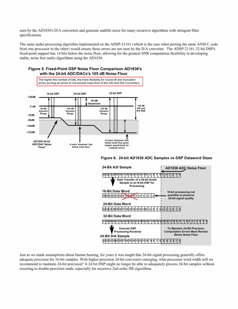
seen by the AD1836's D/A converters and generate audible noise for many recursive algorithms with stringent filter specifications. The same audio processing algorithm implemented on the ADSP-21161 (which is the case when porting the same ANSI C code from one processor to the other) would ensure these errors are not seen by the D/A converter. The ADSP-21161 32-bit DSP's fixed-point support has 14 bits below the noise floor, allowing for the greatest SNR computation flexibility in developing stable, noise free audio algorithms using the AD1836.
Figure 5. Fixed-Point DSP Noise Floor Comparison AD1836's with the 24-bit ADC/DACs's 105 dB Noise Floor
16-bit DSP 32-bit DSP 24-bit DSP
0 dB 96 dB
Dynamic Range
144 dB Dynamic Range
192 dB Dynamic
Range
AD1836 24-bit ADC/DAC Noise
“Floor”
20 dB Headroom
The higher the number of bits, the more flexibility for round-off and truncation errors as long as errors to not exceed noise floor of the A/D and D/A Converters.
105 dB A/D and D/A SNR
+20dB
-72dB
-85dB
-124dB
-172dB
14 extra ‘footroom’ bits below noise floor gives largest ‘guard-band’ for
compute errors 6 extra ‘footroom’ bits
below noise floor
Figure 6. 24-bit AD1836 ADC Samples vs DSP Dataword Sizes
24-Bit A/D Sample
31 30 29 28 27 26 25 24 23 22 21 2019 18 17 16 15 14 13 12 11 10 9 8 7 6 5 4 3 2 1 0 32-Bit Data Word
AD1836 ADC Noise Floor
Data Transfer of a 24-bit Audio Sample to an N-bit DSP for
Processing
To Maintain 24-Bit Precision, Computation Errors Must Remain
Below Noise Floor
1514 13 12 11 10 9 8 7 6 5 4 3 2 1 0
16-Bit Data Word
23 22 21 2019 18 17 16 15 14 13 12 1110 9 8 7 6 5 4 3 2 1 0
24-Bit Data Word
23 22 21 2019 18 17 16 15 14 13 12 1110 9 8 7 6 5 4 3 2 1 0
Execute DSP Processing Routines
24-Bit D/A Sample 23 22 21 2019 18 17 16 15 14 13 12 11 10 9 8 7 6 5 4 3 2 1 0
16-bit processing not possible to preserve 24-bit signal quality
Just as we made assumptions about human hearing, for years it was taught that 24-bit signal processing generally offers adequate precision for 16-bit samples. With higher-precision 24-bit converters emerging, what processor word width will we recommend to maintain 24-bit precision? A 24 bit DSP might no longer be able to adequately process 24-bit samples without resorting to double-precision math, especially for recursive 2nd-order IIR algorithms.
R. Wilson [3] and Chen [7] demonstrated that even for recursive second order IIR filter computations on a 24-bit DSP, the noise floor of the digital filter can still go above that of the 16-bit sample and hence become audible. To compensate for this the use of error feedback schemes or double precision arithmetic were required. So what are the implications of the fact that 24-bit computations can introduce noise artifacts that can go above a 16-bit noise floor for complex 2nd- order filters? We can conclude when a 24-bit DSP processes 24-bit samples, that unless you take precautions a digital filter’s noise floor is always greater than the converter's noise floor. These costly error-feedback schemes and double-precision arithmetic are unavoidable and can add significant overhead when processing 24-bit audio data. When considering the AD1836's 24-bit data conversion capability for a potential new audio design, the use of a native 32-bit fixed-point support becomes necessary for critical frequency response designs to ensure that a filter algorithm’s quantization noise artifacts will not exceed the AD1836's 24-bit 105 dB input signal. Indeed, newer 24-bit converter technology makes a strong case for 32-bit DSP processing, and such DSPs are already becoming the processor of choice for many audio equipment manufacturers who work with 24-bit signal conversion. The ADSP-21161 SIMD architecture enables efficient coding of audio algorithms by taking advantage of two identical sets of computation units. Each computation unit section, or processing element, gives the DSP audio engineer the ability to efficiently process complex stereophonic algorithms concurrently by operating on left channel data in one processing element and the right channel data in the other processing element. Single channel block processing operations such those that are used in FFT or block FIR algorithms can be evenly distributed between both processing elements to improve algorithmic execution by as much as 80-90 % over SISD mode when 1 computation unit is enabled. In addition, the ADSP-21161 includes desirable peripheral enhancements to perform real-time audio computations, including: • Native 32-bit fixed and 32-/40 bit floating point support. With the use of 32-bit filter coefficients, giving precise
placement of poles and zeros while ensuring that the digital filters noise floor remains below that of the ADC/DAC. • Fast and flexible arithmetic with the use of a 2 DSP computation cores, which are also called Processing Elements. Each
Processing Element (PEX and PEY) consists of an ALU, multiplier, shifter and register file. These dual PEs provide more computational horse power to execute the basic building blocks of audio algorithms; such as FIR filters, IIR filters, and FFT processing.
• Extended dynamic range for extended sum-of-product calculations with four 80-bit fixed-point accumulators Single-cycle fetch of four operands for two sum-of-products calculations in SIMD mode.
• Hardware circular buffer support for up to 32 concurrent audio delay-lines (16 primary, 16 alternate), which is beneficial for certain audio applications requiring the use of a large number of delay-line pointers
• Efficient looping and branching for repetitive DSP operations through an optimized Program Sequencer • 1 Megabit on-chip SRAM, and an on-chip SDRAM controller providing low-cost bulk storage for code and lengthy delay
lines for time-delay effects and digital filters • Integrated glueless multiprocessing support for large signal processing systems such as 64 channel mixers • 4 SPORTs with I2S support, providing two data pins, which can be programmable as transmitters or receivers. The I2S
enhancement and data path programmability of the serial data pins allows the designer to configure the SPORTs for 16 I2S transmit channels, or 16 I2S receive channels, or a combination of 12 transmit/8 receive, 8 transmit- 8 receive, or 4 transmit- 8 receive I2S channels. I2S is an industry-wide standard which provides a glueless interconnection to a wide variety of ADCs, DACs, SP/DIF or AES/transmitter and receivers used in a variety of pro and consumer audio applications.

Figure 7. ADSP-21161 Architecture Block Diagram
The complexity of DSP algorithms increases with the introduction of new audio standards and requirements, and designers are looking to 24-bit converters like the AD1836 to increase signal quality in their low-cost multichannel audio applications. To preserve the quality of 24-bit samples requires at least 32 bits during signal processing is recommended to ensure that the algorithm’s noise floor won’t exceed the 24-bit input signal. With the AD1836's 24-bit audio data, the ADSP-21161's 32-bit processing is especially useful for complex math-intensive or recursive processing with IIR filters. For example, parametric and graphic equalizer implementations using cascaded 2nd-order IIR filters, and comb/allpass filters for audio are more robust using 32-bit math. The ADSP-21161's 32-bit processing can remove many implementation restrictions on the filter structure that might be present for smaller width DSPs, resulting in smaller sized, faster algorithms. Designers can select any filter structure without worrying about the level of the noise floor, thereby eliminating the need for double-precision math and error-feedback schemes. With a 32-bit DSP like the ADSP-21161, providing 14 bits below the noise floor, quantization errors would have to accumulate to 86 dB from the LSB of the 32-bit word before the AD1836's DACs could see them. To maintain high audio-signal quality well above the 105 dB noise floor of the AD1836, the ADSP-21161 EZ-KIT Lite system is an excellent reference design which enables the DSP programmer to implement algorithms such that all intermediate DSP calculations using a precision higher than the bit length of the quantized input data, using either 32-bit fixed point or 32-bit/40-bit floating point processing. The ADSP-21161 also provides the ability to use high-precision 40-bit storage between the DSP's memory and computation units for extended precision floating point operations. The use of optimal (low-noise) filter algorithms, higher precision filter coefficients and higher precision storage of intermediate samples (available with 80-bit extended precision in the MAC unit) ensure that errors that arise during ADSP-21161 arithmetic computations are much smaller than the error introduced by the AD1836 D/As when it generates an output signal. We then ensure that the ADSP-21161's digital-filter’s noise floor will be lower than the resolution of the AD1836 data converters, and in many cases in many cases the only limiting factor to maintaining a high digital audio system SNR is only the precision of the AD1836's 24-bit data converters. Clearly, systems built with the AD1836 implementing complex, recursive algorithms will require at least 32-bit processing to ensure that a filter algorithm's quantization noise artifacts won’t exceed the 24-bit input signal. The ADSP-21161 is an attractive 32-bit alternative with it's SIMD architecture and rich peripheral set. With optimal filter implementations, the AD1836's 24-bit D/As never will see any quantization noise introduced in the 32-bit computations generated by the ADSP-21161. In many cases, an audio designer can choose from several 2nd-order structures which may be faster but are more susceptible to generating noise, as long as the accuracy of the arithmetic result remains greater than the 105 dB. Thus, the 32-bit processing capability of the ADSP-21161 guarantees that the noise artifacts remain below the AD1836's 105-dB noise floor and hence maintains the dynamic range of the audio signal.
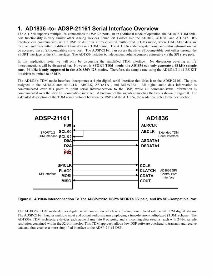
1. AD1836 -to- ADSP-21161 Serial Interface Overview The AD1836 supports multiple I2S connections to DSP I2S ports. In an additional mode of operation, the AD1836 TDM serial port functionality is very similar other Analog Devices SoundPort Codecs like the AD1819, AD1881 and AD1847. It’s interface can communicates with a DSP or ASIC in a time-division multiplexed (TDM) mode, where DAC/ADC data are received and transmitted in different timeslots in a TDM frame. The AD1836 codec register command/status information can be accessed via an SPI-compatible slave port. The ADSP-21161 can access the slave SPI-compatible port either through the SPORT interface or the SPI interface. The AD1836 includes 6, independent volume controls adjustable via the SPI slave port.
In this application note, we will only be discussing the simplified TDM interface. No discussion covering an I2S interconnections will be discussed her. However, in SPORT TDM mode, the AD1836 can only generate a 48 kHz sample rate. 96 kHz is only supported in the AD1836's I2S modes. Therefore, the sample rate using the AD1836/21161 EZ-KIT lite driver is limited to 48 kHz.
The AD1836's TDM mode interface incorporates a 4 pin digital serial interface that links it to the ADSP-21161. The pins assigned to the AD1836 are: ALRCLK, ABCLK, ASDATA1, and DSDATA1. All digital audio data information is communicated over this point to point serial interconnection to the DSP, while all command/status information is communicated over the slave SPI-compatible interface. A breakout of the signals connecting the two is shown in Figure 8. For a detailed description of the TDM serial protocol between the DSP and the AD1836, the reader can refer to the next section.
AD1836 ADSP-21161
ABCLK SCLK0 SCLK2
ASDATA1 D0A DSDATA1
FS0
D2A
ALRCLK
FS2
AD1836 SPI Control Port
Interface
CCLK CLATCH CDATA COUT
FLAG0 MOSI MISO
SPICLK
SPI Interface
SPORT0/2 TDM Interface
Extended TDM Serial Interface
Figure 8. AD1836 Interconnection To The ADSP-21161 DSP's SPORTs 0/2 pair, and it's SPI-Compatible Port
The AD1836's TDM mode defines digital serial connection which is a bi-directional, fixed rate, serial PCM digital stream. The ADSP-21161 handles multiple input and output audio streams employing a time-division-multiplexed (TDM) scheme. The AD1836's TDM architecture divides each audio frame into 8 outgoing and 8 incoming data streams, each with 24-bit sample resolution contained within the 32-bit timeslot. This TDM approach allows low DSP software overhead to transmit and receive data and thus enables a more simplified interface to the ADSP-21161 DSP.

1.1 AD1836 Serial Port Clocks And Frame Sync Rates
To keep clock jitter to a minimum, the AD1836 derives its clock internally from an externally attached 12.288 MHz crystal (24.576 MHz if generating 96 kHz sample rates) and drives a buffered clock to the ADSP-21161 over the serial link under the signal name ABCLK. Clock jitter at the AD1836 DACs and ADCs is a fundamental impediment to high quality output, and the internally generated clock provided the AD1836 with a clean clock that is independent of the physical proximity of the ADSP-21161 processor. ABCLK, fixed at 12.288 MHz, provides the necessary clocking granularity to support 8, 32-bit outgoing and incoming time slots with a selected sample rate of 48 kHz. The TDM serial data is transitioned on each rising edge of ABCLK. The receiver of TDM data, AD1836 for outgoing data and the ADSP-21161 for incoming data, samples each serial bit on the falling edges of ABCLK. The AD1836 drives the serial bit clock at 12.288 MHz, which the ADSP-21161 then qualifies with a synchronization signal to construct audio frames.
The beginning of all audio sample packets, or “Audio Frames”, transferred over the TDM link is synchronized to the rising edge of the FSTDM (ALRCLK) signal. In TDM mode, the ALRCLK pin is renamed as the FSTDM pin. The FSTDM (ALRCLK) pin is used for the serial interface frame synchronization and is generated by the AD1836 as an input to the ADSP-21161. Synchronization of all TDM data transactions is signaled by the ADSP-21161 via the FS0 signal. FSTDM, fixed at 48 kHz, is derived by dividing down the serial bit clock (ABCLK). The ADSP-21161 takes SCLK0 (ABCLK) and FS0 (FSTDM) as inputs. A frame sync is generated once every 256 SCLK0 cycles, which yields a 48kHz FSTDM signal whose period defines an audio frame. The FSTDM (FS0) pulse is driven by the AD1836 codec. To accept both an externally generated 48 kHz frame sync with an externally generated 12.288 MHz SCLK, the DSP must the corresponding bits to a 1 in the SPCTL registers to accept these externally generated signals. The AD1836's frame rate is always equivalent to the sample rate of operation, i.e., a 48 kHz frame rate means we are transmitting and receiving audio data at a rate of a 48 kHz sample rate. The ASDATA1 and DSDATA1 pins handle the serial data input and output of the AD1836. Both the AD1836’s ASDATA1 and DSDATA1 pins transmit or receive data on 8 different timeslots per audio frame. The AD1836 transmits data on every rising edge of ABCLK (SCLK0) and it samples received data on the falling edge of ABCLK (SCLK0).

2. AD1836/ADSP21161 EXT-TDM Digital Serial Interface Protocol The Extended TDM Mode protocol described in the AD1836 data sheet provides for a 8x32bit timeslots-bit time slot.
ASDATA1 (D0A)
DSDATA1 (D2A) Outgoing
FSTDM (FS0)
Timeslot # 0 1 2 3 4 5 6 7
ABCLK (RCLK0 & TCLK2)
BCLK not to scale- 256 BCLKs per
Internal DAC Left 0
Internal DAC Left 1
= Gray area indicates conversion resources internal to the AD1836 FS2 (TVD2) unconnected in multichannel mode For the 21161, the serial clocks are internally connected in multichannel mode.
Internal DAC Right0
Internal DAC Right1
Internal DAC Left
Internal DAC Right2
Auxiliary DAC Left
Auxiliary DAC R0
Internal ADC Left 0
Internal ADC Left 1
Intern ADC Right 0
Intern ADC Right 1
Auxiliary ADC Left
Auxiliary ADC R0
Auxiliary ADC Left
Auxiliary ADC R1
32-
Figure 9. AD1836 Extended TDM Mode Bi-directional Audio Frame
The Extended TDM protocol for the 21161 EZ-KIT Lite makes use of 1 auxiliary input device - the CS8414 SP/DIF receiver, and 1 auxiliary output device - the AD1852 DAC. See fig x for a functional block diagram of the EZ-KIT Lite audio interface.
ASDATA1 (D0A)
DSDATA1 (D2A) Outgoing
FSTDM (FS0)
Timeslot # 0 1 2 3 4 5 6 7
ABCLK (RCLK0 & TCLK2)
BCLK not to scale- 256 BCLKs per
Internal DAC Left 0
Internal DAC Left 1
= Gray area indicates conversion resources internal to the AD1836 X = Indicates inactive timeslot, no external auxiliary device connected
Internal DAC Right0
Internal DAC Right1
Internal DAC Left
Internal DAC Right2
AD1852 DAC Left
AD1852 DAC R0
Internal ADC Left 0
Internal ADC Left 1
Intern ADC Right 0
Intern ADC Right 1
CS8414 SP/DIF Left
CS8414 SP/DIF R0 X X
32-
Figure 10. Modified AD1836 Extended TDM Bi-directional Audio Frame For The 21161 EZ-KIT Lite

AD1836 AD1852
DAC
L R
RCA Phono Line Out Connectors
CS8414
SSM2275 Stereo Amps
R2 L2 R1 L1 R0 L0
SSM2275 Stereo Amps
RCA Phono Line In JACKs
L0
R0
R1
L1
I2S I2S
Optional 1/8th Inch MIC jack
for ADC0
Optional 1/8th Inch
Headphone Out Jack for
DAC0 L/R
TORX173 Optical
Receiver
ADSP-21161N SPORT0 SPORT2
TDM Mode Interface
DACAUX Out
ADC AUX In
Figure 11. ADSP-21161 EZ-KIT Lite Audio Interface (Extended TDM Mode with 2 Auxiliary Devices)
2.1 ADSP21161 / AD1836 Audio Output Frame (D2A to DSDATA1) The audio output frame data streams correspond to the multiplexed bundles of all digital output data targeting the AD1836 DAC inputs. Each audio output frame can support up to 8, 32-bit outgoing data time slots. The following diagram illustrates the timeslot-based protocol.
FSTDM (FS0)
ABCLK (SCLK2)
DSDATA1 (D2A) 30
Slot 0
20.8uS (48 KHz)
Slot 1 Slot 2
0 31 0 31 0 31 0
Slot 3 Slot 7
81.4 nS 12.288
MHz
29 0 1 2 3 31
Start of new Audio Frame
End of previous Audio Frame
31
Figure 12. AD1836 TDM Audio Output Frame - ADSP-21161 to AD1836

A new audio output frame begins with a low to high transition of FSTDM. FSTDM is synchronous to the rising edge of ABCLK. On the immediately following falling edge of ABCLK, the ADSP-21161 samples the assertion of FSTDM. This falling edge marks the time when both sides the TDM link are aware of the start of a new audio frame. On the next rising of ABCLK, the ADSP-21161 transitions DSDATA1 into the first bit position of slot 0 (MSB). Each new bit position is presented to the TDM link on a rising edge of ABCLK, and subsequently sampled by AD1836 on the following falling edge of ABCLK. This sequence ensures that data transitions, and subsequent sample points for both incoming and outgoing data streams are time aligned.
FSTDM
DSDATA1 D31 D30 D29
End of previous Audio Frame
AD1836 generates frame sync assertion here
ADSP-21161 drives first DSDATA1 bit of
frame here ABCLK
D2A
SCLK2
FS0
Figure 13. Start of an Audio Output Frame
D2A/DSDATA’s composite stream is MSB justified (MSB first) with all non-valid slots’ bit positions stuffed with 0’s by the ADSP-21161. The DSP software initializes the transmit DMA buffer to 0s in the AD1836 driver. (shown in Appendix A). The 24-bit audio data contained within the 32-bit timeslot is left justified, i.e., the 24-bit information processed by the AD1836 DACs reside in bit positions 31 to 8.
In the event that there are less than 32-valid bits within an assigned and valid time slot, the ADSP-21161 always stuff all trailing non-valid bit positions of the 32-bit slot with 0’s.
When mono audio sample streams are output from the ADSP-21161, the programmer can optionally ensure that each left and right sample stream pair time slots be filled with the same data.
2.2 AD1836/ADSP-21161 Audio Input Frame (SDATA_IN to DR0) The audio input frame data streams correspond to the multiplexed bundles of all digital input data targeting the ADSP-21161. As is the case for audio output frame, each AD1836 audio input frame consists of 8, 32-bit time slots. The following diagram illustrates the time slot based AD1836 TDM protocol:
FSTDM (FS0)
ABCLK (SCLK0)
ASDATA1 (D0A) 30
Slot 0
20.8uS (48 KHz)
Slot 1 Slot 2
0 31 0 31 0 31 0
Slot 3 Slot 7
81.4 nS 12.288
MHz
29 0 1 2 3 31
Start of new Audio Frame
End of previous Audio Frame
31
Figure 14. AD1836 TDM Audio Input Frame - AD1836 to ADSP-21161

The audio input frame (data samples sent to the DSP from the AD1836) begins with a low to high transition of FSTDM (FS0). FSTDM is synchronous to the rising edge of ABCLK (SCLK0). On the immediately following falling edge of ABCLK, the AD1836 generates the assertion of FSTDM. This falling edge marks the time when both sides of serial link are aware of the start of a new audio frame. On the next rising of ABCLK, the AD1836 transitions ASDATA1 into the first bit position of slot 0. Each new bit position is presented to the TDM link on a rising edge of ABCLK, and subsequently sampled by the ADSP-21161 on the following falling edge of ABCLK. This sequence ensures that data transitions, and subsequent sample points for both incoming and outgoing data streams are time aligned. The ASDATA1's composite stream is MSB justified (MSB first) with all non-valid slot positions (for assigned and/or unassigned time slots) stuffed with 0’s by the AD1836. ASDATA1 data is sampled on the falling edges of ABCLK.
FSTDM
ASDATA1 D31 D30 D29
End of previous Audio Frame
ADSP-21161 samples SYNC assertion here ADSP-211161 DSP samples
first ASDATA1 bit of frame here
ABCLK
D0A
SCLK0
FS0
Figure 15. Start of an Audio Input Frame
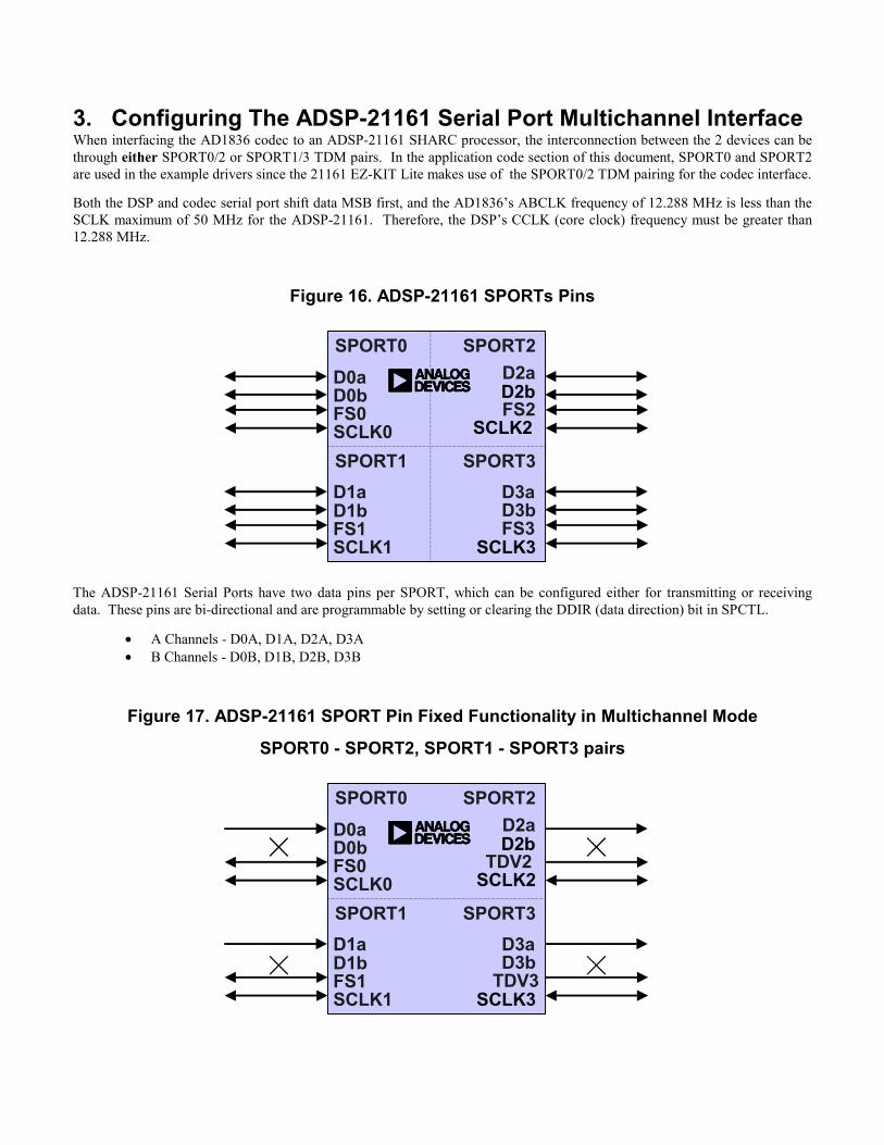
3. Configuring The ADSP-21161 Serial Port Multichannel Interface When interfacing the AD1836 codec to an ADSP-21161 SHARC processor, the interconnection between the 2 devices can be through either SPORT0/2 or SPORT1/3 TDM pairs. In the application code section of this document, SPORT0 and SPORT2 are used in the example drivers since the 21161 EZ-KIT Lite makes use of the SPORT0/2 TDM pairing for the codec interface.
Both the DSP and codec serial port shift data MSB first, and the AD1836’s ABCLK frequency of 12.288 MHz is less than the SCLK maximum of 50 MHz for the ADSP-21161. Therefore, the DSP’s CCLK (core clock) frequency must be greater than 12.288 MHz.
Figure 16. ADSP-21161 SPORTs Pins
D2a D2b FS2
SCLK2
D3a D3b FS3
SCLK3
D0b FS0 SCLK0
D1b FS1 SCLK1
D0a
D1a
SPORT0 SPORT2
SPORT1 SPORT3
aaaa
The ADSP-21161 Serial Ports have two data pins per SPORT, which can be configured either for transmitting or receiving data. These pins are bi-directional and are programmable by setting or clearing the DDIR (data direction) bit in SPCTL.
• A Channels - D0A, D1A, D2A, D3A • B Channels - D0B, D1B, D2B, D3B
Figure 17. ADSP-21161 SPORT Pin Fixed Functionality in Multichannel Mode
SPORT0 - SPORT2, SPORT1 - SPORT3 pairs
D2a D2b
TDV2 SCLK2
D3a D3b
TDV3 SCLK3
D0b FS0 SCLK0
D1b FS1 SCLK1
D0a
D1a
SPORT0 SPORT2
SPORT1 SPORT3
aaaa

Table 1. ADSP-21161 SPORT0/2 TDM Configuration
Transmit data X D2A X
Transmit clock SCLK1
Transmit frame sync/ X (redefined as TVD2) word select
Receive data D0A X X
Receive clock SCLK0
Receive frame sync FS0
Function Function A Chn A Chn B Chn B Chn SPORT0 SPORT0
A Chn A Chn B Chn B Chn SPORT1 SPORT2
NOTE: The ADSP-21161 SPORT channel B pins are not functional for multichannel mode. Both the transmitter and receiver have their own serial clocks. The FS2/FS3 frame syncs become output transmit data valid pins, while FS0/FS1 pins are used to control the start of a multichannel frame.
ALRCLK
ABCLK
DSDATA1
ASDATA1
ADSP-21161 SCLK0
FS0
D2A
D0A
TX2A
RX0A
SPORT DMA Transfers
Internal DM
AD1836 SCLK2
Figure 18. Typical AD1836/ADSP-21161 SHARC Serial Port Interconnections (assuming 3.3V I/0 Supply Voltage on the AD1836)
NOTE: The ADSP-21161’s FS2 line is an output pin in multichannel mode(TDV2 - Transmit Data Valid). It should be left unconnected and not tied with FS0 together to the AD1836 Frame Sync. This could cause contention on the FS0 (FSTDM) and will most likely lock up the SPORT and possibly damage the FS0 pin!!!

3.1 ADSP-21161 - 3.3 V Level Shifting Considerations The ADSP-21161 is a new derivative of the ADSP-2116x SIMD SHARC family which is based on a .18 micron CMOS process, and is a dual voltage part operating at a 1.8 volt core and 3.3 volt I/O. Since the ADSP-21161 is a dual voltage part, the 5 volt signals that the AD1836 provides will damage the driver pins on the 21161 serial ports, which operate at 3.3 volts. Two options are available to prevent this. The AD1836's digital interface can optionally operate with a digital I/O supply voltage of 3.3 volts. Thus no level shifting is required, making this the optimal method because no glue logic is required. To implement a glueless interface, the AD1836's ODVDD can be connected to the system's 3.3 volt supply instead of the 5 volt supply. All AD1836 Digital I/O drivers will then operate at 3.3 volts. Another option is to level-shifting of all input signals from the AD1836. All SPORT output signals that are inputs to the AD1836 do not need to be level shifted since the AD1836 will recognize 3.3 volts as a valid TTL high level.
Figure 19. 21161 Optional Codec Interface with a 5 Volt Digital I/O Supply
74LV125
AD1836 ADSP-21161
ABCLK SCLK0 SCLK2
ALRCLK FS0
ASDATA1 DSDATA12
D2A D0A
3.3V-to-5V Level
Translator
In order to facilitate serial communications with the AD1836, the SPORT0 and SPORT2 pin connections are configured as shown in Table 1 and Figure 9:
Table 2. ADSP-21161N Pin: AD1836 Pin: Driven By:
SCLK0, SCLK2 ABCLK codec
FS0 FSTDM (ALRCLK) codec
FS2 [TDV2] ( unconnected ) ---------- ----------
D0A ASDATA1 codec
D2A DSDATA1 DSP

3.2 SPORT DMA Channels And Interrupt Vectors There are 8 dedicated DMA channels for SPORT0, SPORT1, SPORT2, and SPORT3 on the ADSP-21161. The IOP addresses for the DMA parameter registers are shown in the table below for each corresponding channel and SPORT data buffer. In multichannel mode, only channels 0, 2, 4 and 6 are activated, because the channel B pins are disabled in Multichannel Mode.
Table 3. 8 SPORT DMA channels and data buffers
Chan Data Buffer Address Description
0 RX0A/TX0A 0x0060 0x0064 Serial port 0 rx or tx; A data
1 RX0B/TX0B 0x0080 0x0084 Serial port 0 rx or tx; B data
2 RX1A/TX1A 0x0068 0x006C Serial port 1 rx or tx; A data
3 RX1B/TX1B 0x0088 0x008C Serial port 1 rx or tx; B data
4 RX2A/TX2A 0x0070 0x0074 Serial port 2 rx or tx; A data
5 RX2B/TX2B 0x0090 0x0094 Serial port 2 rx or tx; B data
6 RX3A/TX3A 0x0078 0x005C Serial port 3 rx or tx; B data
7 RX3B/TX3B 0x0098 0x009C Serial port 3 rx or tx; B data
Each serial port buffer and data pin has an assigned TX/RX DMA interrupt (shown in Table 4 below). With serial port DMA disabled, interrupts occur on a word by word basis, when one word is transmitted or received. Table 4 also shows the interrupt priority, because of their relative location to one another in the interrupt vector table. The lower the interrupt vector address, the higher priority the interrupt. Note that channels A and B for each SPORT share the same interrupt location. Thus, data for both DMA channels (or SPORT data buffers A & B) is processed at the same time, or on a conditional basis depending on the state of the buffer status bits in the SPORT control registers.
Table 4. ADSP-21161 Serial Port Interrupts
SP0I SPORT0 TX or RX DMA channels 0 and 1
SP1I SPORT1 TX or RX DMA channels 2 and 3
SP2I SPORT2 TX or RX DMA channels 4 and 5
SP3I SPORT3 TX or RX DMA channels 6 and 7
Interrupt 1 Function Priority
Lowest
1 Interrupt names are defined in the def21161.h include file supplied with the ADSP-21000 Family Visual DSP Development Software.
Highest
DMA channels 8 to 13 are used for Link Ports, SPI and External Port DMA

3.3 Serial Port Related IOP Registers This section briefly highlights the list of available SPORT-related IOP registers that are required to be programmed when configuring the SPORTs for Multichannel Mode on the 21161 EZ-KIT lite in order to communicate with the AD1836 via SPORT0 and SPORT2. To program these registers, you write to the appropriate address in memory using the symbolic macro definitions supplied in the def21161.h file (included with the Visual DSP tools in the /INCLUDE/ directory). External devices such as another ADSP-21161, or a host processor, can write and read the SPORT control registers to set up a serial port DMA operation or to enable a particular SPORT. These registers are listed in Table 5 below. The SPORT DMA IOP registers are covered in section 4.8. As we will see in the next section, many of the available registers shown below need to be programmed to set up Multichannel Mode. These registers are highlighted in bold text.
Table 5. Serial Port IOP Registers for SPORT0/SPORT2 MCM Pairing Register IOP Address Description SPORT0 SPCTL0 0x1C0 SPORT0 control register
DIV0 0x1C5 SPORT0 clock and frame sync divisor MR0CS0 0x1C7 SPORT0 multichannel receive select 0 (channels 31-0) MR0CS1 0x1C9 SPORT0 multichannel receive select 1 (channels 63-32) MR0CS2 0x1CB SPORT0 multichannel receive select 2 (channels 95-64) MR0CS3 0x1CD SPORT0 multichannel receive select 3 (channels 127-96) MR0CCS0 0x1C8 SPORT0 multichannel receive compand select 0 (channels 31-0) MR0CCS1 0x1CA SPORT0 multichannel receive compand select 1 (channels 63-32) MR0CCS2 0x1CC SPORT0 multichannel receive compand select 2 (channels 95-64) MR0CCS3 0x1CE SPORT0 multichannel receive compand select 3 (channels 127-96)
SPORT2 SPCTL2 0x1D0 SPORT2 control register DIV2 0x1D5 SPORT2 clock and frame sync divisor MT2CS0 0x1D7 SPORT2 multichannel transmit select 0 (channels 31-0) MT2CS1 0x1D9 SPORT2 multichannel transmit select 1 (channels 63-32) MT2CS2 0x1DB SPORT2 multichannel transmit select 2 (channels 95-64) MT0CS3 0x1DD SPORT2 multichannel transmit select 3 (channels 127-96) MT2CCS0 0x1D8 SPORT2 multichannel transmit compand select 0 (channels 31-0) MT2CCS1 0x1DA SPORT2 multichannel transmit compand select 1 (channels 63-32) MT2CCS2 0x1DC SPORT2 multichannel transmit compand select 2 (channels 95-64) MT2CCS3 0x1DE SPORT2 multichannel transmit compand select 3 (channels 127-96)
SP02MCTL 0x1DF SPORT 0/2 Multichannel Control Register Within the 4 SPORTs on the ADSP-21161, there are 16 SPORT data buffers associated with the 16 serial data pins. In Multichannel Mode, the available SPORT data buffers are active are the channel A registers (which are highlighted below) only. It is these registers that are actually used to transfer data between the AD1836 and the DMA controller on the ADSP-21161. The DMA controller is used to transfer data to and from internal memory without any intervention from the core. SPORT TX0A 0x1C1 SPORT0 transmit data buffer, channel A data Data TX0B 0x1C2 SPORT0 transmit data buffer, channel B data Buffers RX0A 0x1C3 SPORT0 receive data buffer, channel A data
RX0B 0x1C4 SPORT0 receive data buffer, channel B data TX2A 0x1D1 SPORT2 transmit data buffer, channel A data TX2B 0x1D2 SPORT2 transmit data buffer, channel B data RX2A 0x1D3 SPORT2 recieve data buffer, channel A data RX2B 0x1D4 SPORT2 receive data buffer, channel B data

3.4 SPORT0/SPORT2 IOP Register Configurations For Audio Processing At 48 kHz The configuration for SPORT0 and SPORT2, for use with the ADSP-21161 EZ-KIT Lite at a fixed 48 kHz sample rate, is set up as follows: • 32-bit serial word length • Enable SPORT0 receive A channel DMA functionality • Enable SPORT2 transmit A channel DMA functionality • Enable DMA chaining functionality for SPORT0 receive A channel and SPORT2 transmit A channel • External Serial Clock (SCLK0) - the codec provides the serial clock to the ADSP-21161. • Transmit and Receive DMA chaining enabled. The DSP program declares 2 buffers - rx_buf0a[8] and tx_buf2a[0] - for
DMA transfers of SPORT0/2 receive and transmit serial data. Both buffers reserve 8 locations in memory to reflect the AD1836 time slot allocation for the codec. DMA chaining is almost certainly required (and strongly recommended), or the interrupt service overhead will chew up too more of the DSP’s bandwidth.
• Multichannel Frame Delay = 1, i.e., the frame sync occurs 1 SCLK cycle before MSB of 1st word/timeslot in the audio TDM frame. New frames are marked by a HI pulse driven out on FSTDM one serial clock period before the frame begins.
Program_SPORT02_TDM_Registers: /* SPORT0 and SPORT2 are being operated in "multichannel" mode. This is synonymous with TDM mode which is the operating mode for the AD1836 */ /* SPORT 0&2 Miscellaneous Control Bits Registers */ R0 = NCH_8 | MFD1; /*Hold off on MCM enable, and no of TDM slots to 8 active channels*/ dm(SP02MCTL) = R0; /*Multichannel Frame Delay=1, Number of Channels = 8, LB disabled*/
/* sport0 control register set up as a receiver in MCM */ R0 = SCHEN_A | SDEN_A | SLEN32; dm(SPCTL0) = R0; /* sport 0 control register SPCTL0 = 0x000C01F0 */ /* sport2 control register set up as a transmitter in MCM */ R0 = SCHEN_A | SDEN_A | SLEN32; dm(SPCTL2) = R0; /* sport 2 control register, SPCTL2 = 0x000C01F0 */
• The ADSP-21161 shifts it's data based on an externally generated 48 kHz frame sync (FS0). It is actually a 48 kHz frame
rate since the AD1836 TDM sample rate operates at 48 kHz (NOTE: 96 kHz in TDM mode is not supported). Since the AD1836 serial clock is 12.288 MHz, a divide factor or 256 (256xFs) will produce a 48 kHz internally generated frame sync.
/* sport 0 & 2 frame sync divide registers */ /* External Clock and Frame Sync generated by AD1836 */ R0 = 0x00000000; dm(DIV0) = R0; dm(DIV2) = R0;
• No companding.
/*sport0 & sport2 receive & transmit multichannel companding enable registers*/ R0 = 0x00000000; /* no companding for our 8 active timeslots*/ dm(MR0CCS0) = R0; /* no companding on SPORT0 receive */ dm(MR0CCS1) = R0; dm(MR0CCS2) = R0; dm(MR0CCS3) = R0;

dm(MT2CCS0) = R0; /* no companding on SPORT2 transmit */ dm(MT2CCS1) = R0; dm(MT2CCS2) = R0; dm(MT2CCS3) = R0;
• Multichannel Mode - Length = 8 multichannel words enabled. This allows 1 AD1836 frame per ADSP-21161 frame.
/* sport0 & sport2 receive and transmit multichannel word enable registers */ R0 = 0x000000FF; dm(MR0CS0) = R0; /* enable receive channels 0-7 */ dm(MT2CS0) = R0; /* enable receive channels 0-7 */ R0 = 0x00000000; dm(MR0CS1) = R0; /* clear other TDM channels in 128 timeslots*/ dm(MT2CS2) = R0; dm(MT2CS3) = R0; dm(MT2CS1) = R0; dm(MT2CS2) = R0; dm(MT2CS3) = R0;
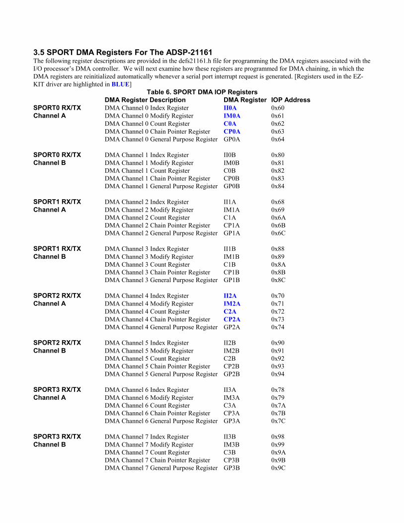
3.5 SPORT DMA Registers For The ADSP-21161 The following register descriptions are provided in the defs21161.h file for programming the DMA registers associated with the I/O processor’s DMA controller. We will next examine how these registers are programmed for DMA chaining, in which the DMA registers are reinitialized automatically whenever a serial port interrupt request is generated. [Registers used in the EZ-KIT driver are highlighted in BLUE]
Table 6. SPORT DMA IOP Registers DMA Register Description DMA Register IOP Address
SPORT0 RX/TX DMA Channel 0 Index Register II0A 0x60 Channel A DMA Channel 0 Modify Register IM0A 0x61
DMA Channel 0 Count Register C0A 0x62 DMA Channel 0 Chain Pointer Register CP0A 0x63 DMA Channel 0 General Purpose Register GP0A 0x64
SPORT0 RX/TX DMA Channel 1 Index Register II0B 0x80 Channel B DMA Channel 1 Modify Register IM0B 0x81
DMA Channel 1 Count Register C0B 0x82 DMA Channel 1 Chain Pointer Register CP0B 0x83 DMA Channel 1 General Purpose Register GP0B 0x84
SPORT1 RX/TX DMA Channel 2 Index Register II1A 0x68 Channel A DMA Channel 2 Modify Register IM1A 0x69
DMA Channel 2 Count Register C1A 0x6A DMA Channel 2 Chain Pointer Register CP1A 0x6B DMA Channel 2 General Purpose Register GP1A 0x6C
SPORT1 RX/TX DMA Channel 3 Index Register II1B 0x88 Channel B DMA Channel 3 Modify Register IM1B 0x89
DMA Channel 3 Count Register C1B 0x8A DMA Channel 3 Chain Pointer Register CP1B 0x8B DMA Channel 3 General Purpose Register GP1B 0x8C
SPORT2 RX/TX DMA Channel 4 Index Register II2A 0x70 Channel A DMA Channel 4 Modify Register IM2A 0x71
DMA Channel 4 Count Register C2A 0x72 DMA Channel 4 Chain Pointer Register CP2A 0x73 DMA Channel 4 General Purpose Register GP2A 0x74
SPORT2 RX/TX DMA Channel 5 Index Register II2B 0x90 Channel B DMA Channel 5 Modify Register IM2B 0x91
DMA Channel 5 Count Register C2B 0x92 DMA Channel 5 Chain Pointer Register CP2B 0x93 DMA Channel 5 General Purpose Register GP2B 0x94
SPORT3 RX/TX DMA Channel 6 Index Register II3A 0x78 Channel A DMA Channel 6 Modify Register IM3A 0x79
DMA Channel 6 Count Register C3A 0x7A DMA Channel 6 Chain Pointer Register CP3A 0x7B DMA Channel 6 General Purpose Register GP3A 0x7C
SPORT3 RX/TX DMA Channel 7 Index Register II3B 0x98 Channel B DMA Channel 7 Modify Register IM3B 0x99
DMA Channel 7 Count Register C3B 0x9A DMA Channel 7 Chain Pointer Register CP3B 0x9B DMA Channel 7 General Purpose Register GP3B 0x9C

3.6 Setting Up The ADSP-21161 DMA Controller For Chained SPORT DMA Transfers To efficiently transmit and receive digital audio data to/from the AD1836, the recommended method is to use "Serial Port DMA Chaining" to transfer data between the serial bus and the DSP core. There are obvious benefits for doing this. First of all, DMA transfers allow efficient transfer of data between the serial port circuitry and DSP internal memory with zero-overhead, i.e. there is no processor intervention of the SHARC core to manually transfer the data. Secondly, there is a one-to-one correspondence of the location of the word in the transmit and receive SPORT DMA buffers with the actual TDM audio frame timeslot on the serial bus. Thirdly, an entire block of data can be transmitted or received before generating a single interrupt. The 'chained-DMA' method of serial port processing is more efficient for the SHARC to process data, versus interrupt driven transfers, which occur more frequently and thus take up more overhead in servicing the audio data. Using chained DMA transfers allows the ADSP-21161 DMA controller to autoinitialize itself between multiple DMA transfers. When the entire contents of the current SPORT buffers rx_buf0a and tx_buf2a have been received or transmitted, the ADSP-21161's I/O processor will automatically set up another serial port DMA transfer that is continuously repeated for every DMA interrupt. For further information on DMA chaining, the reader can refer to "Chaining DMA Processes" section (pages 6-25 to 6-29 I/O Processor Chapter 6) in the ADSP-21161 Hardware Reference. The chain pointer register (CPxxx) is used to point to the next set of TX and RX buffer parameters stored in memory. SPORT DMA transfers for the AD1836 are initiated by writing the DMA buffer's memory address to the CP0A register for SPORT0 receive and CP2A register for SPORT2 transmit. The SCHEN_A and SCHEN_B bits in the SPORTx Control registers enable DMA chaining. To auto-initialize repetitive DMA-chained transfers, the programmer needs to set up a buffer in memory called a transfer control block (TCB) that will be used to initialize and further continue the chained DMA process. Transfer Control Blocks are locations in Internal Memory that store DMA register information in a specified order. For example, Figure 20 below demonstrates defined TCBs in internal memory for SPORT1 Channel A. The Chain Pointer Register (CP0AA and CP2A) stores the location of the next set of TCB parameters to be automatically be downloaded by the DMA controller at the completion of the DMA transfer, which in this case it points back to itself. These TCBs for both the transmit and receive buffers are can be defined in the variable declaration section of your code. In the I2S example code shown in appendix A, the TCBs for SPORT1 channel A are defined as follows: .var rcv1a_tcb[8] = 0, 0, 0, 0, 0, 8, 1, rx_buf0a; /* SPT0 receive tcb */ .var xmit1a_tcb[8] = 0, 0, 0, 0, 0, 8, 1, tx_buf2a; /* SPT2 transmit tcb */
Figure 20. TCBs for Chained DMA Transfers of SPORT1 Channel A Receive and Transmit
rcv0a_tcb[8] xmit2a_tcb[8]
DM(rcv0a_tcb + 0)
DM(rcv0a_tcb + 1)
DM(rcv0a_tcb + 2)
DM(rcv0a_tcb + 3)
DM(rcv0a_tcb + 4)
DM(rcv0a_tcb + 5)
DM(rcv0a_tcb + 6)
DM(rcv0a_tcb + 7)
DM(xmit2a_tcb + 0)
DM(xmit2a_tcb + 0)
DM(xmit2a_tcb + 0)
DM(xmit2a_tcb + 0)
DM(xmit2a_tcb + 0)
DM(xmit2a_tcb + 0)
DM(xmit2a_tcb + 0)
DM(xmit2a_tcb + 0)
ECEPx (not used with SPORTs)
EMEPx (not used with SPORTs)
EIEPx (not used with SPORTs)
GPR1A GPT1A
CPR1A CPT1A
CR1A CT1A
IMR1A IMT1A
IIR1A IIT1A

Note that the count and modified values can be initialized in the buffer declaration so that they are resident after a DSP reset and boot. However, at runtime, further modification of the buffer is required to initiate the DMA autobuffer process. To setup and initiate a chain of SPORT DMA operations at runtime, the ADSP-21161 program should follow this sequence: 1. Set up SPORT transmit and Receive TCBs (transfer control blocks). The TCBs are defined in the data variable declaration
section of your code. Before setting up the values in the TCB and kicking off the DMA process, make sure the SPORT registers are programmed along with the appropriate chaining bits required in step 2.
2. Write to the SPORT0/2 control registers (SPCTL0 and SPCTL2), setting the SDEN_A and/or SDEN_B enable bit to 1 and
the SCHEN_A and/or SCHEN_B chaining enable bit to a 1. 3. Write the address of the Iixxx register of the first TCB to the CPxxx register to start the chain. The order should be as
follows:
a) write the starting address of the SPORT DMA buffer to the TCBs internal index register Iixxx location (TCB buffer base address + 7). You need to get the starting address of the defined DMA buffer at runtime and copy it into this location in the TCB.
b) write the DMA modify register value Imxxx to the TCB (TCB buffer base address + 6). Note that this step may be skipped if it the location in the buffer was initialized in the variable declaration section of your code.
c) write the DMA count register Cxxx value to the TCB (TCB buffer base address + 5). Also note that this step may be skipped if it the location in the buffer was initialized in the variable declaration section of your code.
d) get the Iixxx value of the TCB buffer that was previously stored in step (a), set the PCI bit with a that internal address value, and write the modified value to the chain pointer location in the TCB (TCB buffer base offset + 4).
e) write the same ‘PCI-bit-set’ internal address value from step (d) manually into that DMA channels chain pointer register (CPxxx). At this moment the DMA chaining begins.
The DMA interrupt request occurs whenever the Count Register decrements to zero. SPORT DMA chaining occurs independently for the transmit and receive channels of the serial port. After the SPORT1 receive buffer (rx_buf0a) is filled with new data, a SPORT1 receive interrupt is generated, and the data placed in the receive buffer is available for processing. The DMA controller will autoinitialize itself with the parameters set in the TCB buffer and begin to refill the receive DMA buffer with new data in the next audio frame. The processed data is then placed in the SPORT transmit buffer, where it will then be DMA’ed out from memory to the SPORT DT1A pin. After the entire buffer is transmitted, the DMA controller will autoinitialize itself with the stored TCB parameters to perform another DMA transfer of new data that will be placed in the same transmit buffer (tx_bu2a). Below are the assembly instructions used in the EZ-KIT assembly codec driver (listed in shown in appendix A) to set up the receive transmit DMA buffers and Transfer Control Blocks for SPORT0 and SPORT2 Channel A. These values are reloaded from internal memory to the DMA controller after the entire SPORT DMA buffer has been received or transmitted. SPORT0 is assumed to be configured as a receive DMA channel, while SPORT2 is configured as a transmit DMA channel. .segment /dm dm_codec; /* define DMA buffer sizes to match number of active TDM channels */ .var rx0a_buf[8]; /* receive buffer (DMA)*/ .var tx2a_buf[8] = 0x00000000, /* transmit buffer (DMA)*/ 0x00000000, 0x00000000, 0x00000000, 0x00000000, 0x00000000, 0x00000000, 0x00000000; /* DMA Chaining Transfer Control Block (TCB) */ /* TCB format: Ecx (length of destination buffer),

Emx (destination buffer step size), Eix (destination buffer index (initialized to start address)), GPx ("general purpose"), CPx ("Chain Point register"; points to last address (IIx) of next TCB to jump to upon completion of this TCB.), Cx (length of source buffer), IMx (source buffer step size), IIx (source buffer index (initialized to start address)) */ .var rcv0a_tcb[8] = 0, 0, 0, 0, 0, 8, 1, rx0a_buf; /* SPORT0 receive tcb */ .var xmit2a_tcb[8] = 0, 0, 0, 0, 0, 8, 1, tx2a_buf; /* SPORT2 transmit tcb */ .endseg; .segment /pm pm_code; /*----------------------------------------------------------------------------------*/ /* DMA Controller Programming For SPORT0 and SPORT2 primary A channels */ /*----------------------------------------------------------------------------------*/ Program_SPORT02_DMA_Channels:
r1 = 0x0003FFFF; /* cpx register mask */ /* sport2 dma control tx setup and go */ r0 = xmit2a_tcb + 7; /* get DMA chaining internal mem pointer containing tx_buf address */
r0 = r1 AND r0; /* mask the pointer */ /*(Address will be contained in lower 18 bits (bits 17-0); Upper 13 bits will be zeroed (bits 19-31); Bit 19 is PCI bit ("Program-Controlled Interrupts") */ r0 = BSET r0 BY 18; /* set the pci bit */ dm(xmit2a_tcb + 4) = r0; /* write DMA transmit block chain pointer to TCB buffer */ dm(CP2A) = r0; /* transmit block chain pointer, initiate tx0 DMA transfers */ /* - - - - - - - - - - - - - - - - - - - - - - - - - - - - - - - - - - - - - - - - - - - */ /* - Note: Tshift2 & TX2A will be automatically loaded with the first 2 values in the - */ /* - Tx buffer. The TX buffer pointer ( II2A ) will increment by 2x the modify value - */ /* - ( IM2A ). - */ /* - - - - - - - - - - - - - - - - - - - - - - - - - - - - - - - - - - - - - - - - - - - */ /* sport0 dma control rx setup and go */ r0 = rcv0a_tcb + 7; r0 = r1 AND r0; /* mask the pointer */ r0 = BSET r0 BY 18; /* set the pci bit */ dm(rcv0a_tcb + 4) = r0; /* write DMA receive block chain pointer to TCB buffer*/ dm(CP0A) = r0; /* receive block chain pointer, initiate rx0 DMA transfers */ RTS;
.endseg;

3.7 AD1836 TDM Serial Port Time Slot Assignments and Their DMA Buffer Relationships
The DSP SPORT Multichannel Mode Time Slot Map for AD1836 communication in Extended TDM mode is as follows:
Timeslot DSDATA1 (D2A) Pin - Outgoing Data "Playback" ASDATA1 (D0A) Pin - Incoming Data "Record" 0 Internal DAC0 Left Channel Internal ADC0 Left Channel 1 Internal DAC1 Left Channel Internal ADC1 Left Channel 2 Internal DAC2 Left Channel External Auxiliary ADC0 Left Channel 3 External Auxiliary DAC Left Channel External Auxiliary ADC1 Left Channel 4 Internal DAC0 Right Channel Internal ADC0 Right Channel 5 Internal DAC1 Right Channel Internal ADC1 Right Channel 6 Internal DAC1 Right Channel External Auxiliary ADC0 Right Channel 7 External Auxiliary DAC Right Channel External Auxiliary ADC1 Right Channel
Table 7. AD1836 Extended TDM Mode Timeslot Mapping
Table 8. Corresponding ADSP-21161 SPORT0 DMA Buffer Addresses For Associated Timeslots
rx_buf0a[8] - DSP SPORT DMA receive buffer
Slot # Description Data Memory/DMA Buffer Direct Address Offsets 0 Internal ADC0 Left Channel DM(rx_buf0a + 0) 1 Internal ADC1 Left Channel DM(rx_buf0a + 1) 2 External Auxiliary ADC0 Left Channel DM(rx_buf0a + 2) 3 External Auxiliary ADC1 Left Channel DM(rx_buf0a + 3) 4 Internal ADC0 Right Channel DM(rx_buf0a + 4) 5 Internal ADC1 Right Channel DM(rx_buf0a + 5) 6 External Auxiliary ADC0 Right Channel DM(rx_buf0a + 6) 7 External Auxiliary ADC1 Right Channel DM(rx_buf0a + 7)
tx_buf0a[8] - DSP SPORT DMA transmit buffer
Slot # Description Data Memory/DMA Buffer Direct Address Offsets 0 Internal DAC0 Left Channel DM(tx_buf2a + 0) 1 Internal DAC1 Left Channel DM(tx_buf2a + 1) 2 Internal DAC2 Left Channel DM(tx_buf2a + 1) 3 External Auxiliary DAC Left Channel DM(tx_buf2a + 2) 4 Internal DAC0 Right Channel DM(tx_buf2a + 3) 5 Internal DAC1 Right Channel DM(tx_buf2a + 4) 6 Internal DAC1 Right Channel DM(tx_buf2a + 5) 7 External Auxiliary DAC Right Channel DM(tx_buf2a + 6)

In order to provide easier reading of the AD1836 DSP assembly driver, symbolic macro definitions are defined in order to describe each offset in the DMA buffer, showing it's relationship to the actual TDM timeslot and AD1836 ADC/DAC resource. These are defined as follows: /*AD1836 TDM Timeslot Definitions */ #define Internal_ADC_L0 0 #define Internal_ADC_L1 1 #define AUX_ADC_L0 2 #define AUX_ADC_L1 3 #define Internal_ADC_R0 4 #define Internal_ADC_R1 5 #define AUX_ADC_R0 6 #define AUX_ADC_R1 7 #define Internal_DAC_L0 0 #define Internal_DAC_L1 1 #define Internal_DAC_L2 2 #define AUX_DAC_L0 3 #define Internal_DAC_R0 4 #define Internal_DAC_R1 5 #define Internal_DAC_R2 6 #define AUX_DAC_R0 7
The following figure 21 show the assembly declaration of the SPORT0 receive DMA buffer and the SPORT2 transmit DMA buffer, as well as the symbolic offsets for all AD1836 internal and external auxiliary resources. Figure 21: SPORT RX/TX DMA buffer timeslot representations
rx_buf0a + AUX_ADC_L1
rx_buf0a + Internal_ADC_R0
rx_buf0a + Internal_ADC_R1
rx_buf0a + AUX_ADC_R0
rx_buf0a + AUX_ADC_R1
rx_buf0a + AUX_ADC_L0
rx_buf0a + Internal_ADC_L1
rx_buf0a + Internal_ADC_L0
rx_buf0a[8] Timeslot #
0 1 2 3 4 5 6 7
.segment /dm dm_codec; .var rx_buf0a[8]; // SPORT1 receive DMA buffer .endseg;
tx_buf2a + AUX_DAC_L0
tx_buf2a + Internal_DAC_R0
tx_buf2a + Internal_DAC_R1
tx_buf2a + Internal_DAC_R1
tx_buf2a + AUX_DAC_R0
tx_buf2a + Internal_DAC_L2
tx_buf2a + Internal_DAC_L1
tx_buf2a + Internal_DAC_L0
tx_buf2a[8] Timeslot #
0 1 2 3 4 5 6 7
.segment /dm dm_codec; .var tx_buf2a[8]; // SPORT2 transmit DMA buffer .endseg;

4. Programming the AD1836's Slave SPI Port The AD1836 has an SPI compatible slave control port, which is a four wire serial control port. The format is similar to the Motorola SPI format. This allows the following SPI slave register access options:
1. Programming the internal control registers for the ADCs and DACs 2. Allows reading of ADC peak signal levels through the peak detectors 3. The DAC output levels may be independently programmed by means of an internal attenuator adjustable in 1024 linear
steps. The maximum serial bit clock frequency supported via the AD1836 slave SPI port is 8 MHz. There are two approaches supported on the ADSP-21161 EZ-KIT Lite for programming the AD1836 registers. One is using the ADSP-21161's Serial Peripheral Interface (compatible) port. Another method is currently required is to use "SPI Emulation" using SPORT1 and SPORT3 on the ADSP-21161. This is needed to work around an AD1836 anomaly where the AD1836's CCLK pin needs to be run in continuous mode to work around the AD1836's "extra 17th CCLK" anomaly. Since the SPI protocol uses a gated serial clock, it is difficult to provide the extra clock in order to latch the data, since this is not possible with SPI (In SPI, the serial clock is gated and goes high after the device select is disabled). The 21161's EZ-KIT Lite supports both methods for programming the AD1836 registers. Jumper JP23 connects th4e AD1836 pins to either the SPI port or the SPORT1/SPORT3 pair. With JP23 on, the ADSP-21161's SPORT1 and SPORT3 are interfaced toe the AD1836 SPI port. Removing the jumper connects the ADSP-21161's SPI port to the AD1836's slave SPI port. The block diagrams detailing both approaches are shown below:
AD1836 SPI
Control Port
CCLK
CLATCH
CDATA
COUT
ADSP-21161 FLAG0
MOSI
MISO
SPICLK
Figure 22. AD1836 Port connected to the SPI port (JP23 removed)
AD1836 SPI
Control Port
CCLK
CLATCH
CDATA
COUT
ADSP-21161
SCLK3
FS3
D3A
D1A
SCLK1
FS1
Figure 23. AD1836 Port connected to SPORT1/SPORT3 (JP23 jumper installed)
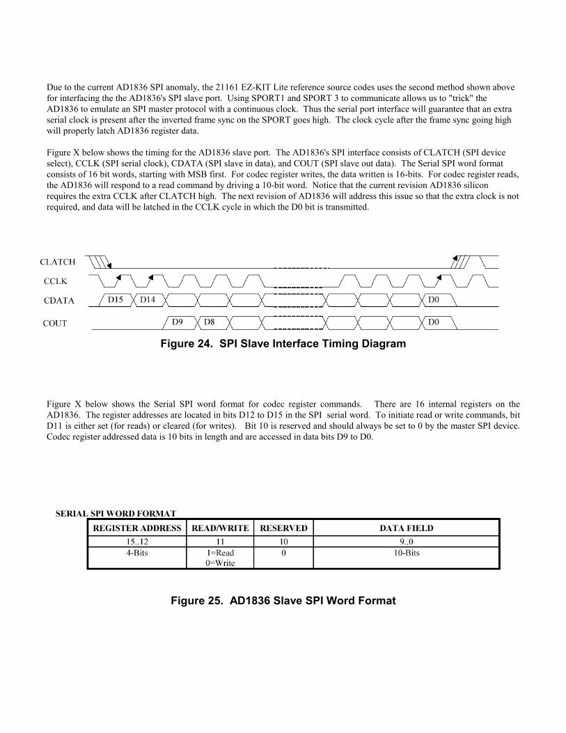
Due to the current AD1836 SPI anomaly, the 21161 EZ-KIT Lite reference source codes uses the second method shown above for interfacing the the AD1836's SPI slave port. Using SPORT1 and SPORT 3 to communicate allows us to "trick" the AD1836 to emulate an SPI master protocol with a continuous clock. Thus the serial port interface will guarantee that an extra serial clock is present after the inverted frame sync on the SPORT goes high. The clock cycle after the frame sync going high will properly latch AD1836 register data. Figure X below shows the timing for the AD1836 slave port. The AD1836's SPI interface consists of CLATCH (SPI device select), CCLK (SPI serial clock), CDATA (SPI slave in data), and COUT (SPI slave out data). The Serial SPI word format consists of 16 bit words, starting with MSB first. For codec register writes, the data written is 16-bits. For codec register reads, the AD1836 will respond to a read command by driving a 10-bit word. Notice that the current revision AD1836 silicon requires the extra CCLK after CLATCH high. The next revision of AD1836 will address this issue so that the extra clock is not required, and data will be latched in the CCLK cycle in which the D0 bit is transmitted.
Figure 24. SPI Slave Interface Timing Diagram
Figure X below shows the Serial SPI word format for codec register commands. There are 16 internal registers on the AD1836. The register addresses are located in bits D12 to D15 in the SPI serial word. To initiate read or write commands, bit D11 is either set (for reads) or cleared (for writes). Bit 10 is reserved and should always be set to 0 by the master SPI device. Codec register addressed data is 10 bits in length and are accessed in data bits D9 to D0.
Figure 25. AD1836 Slave SPI Word Format
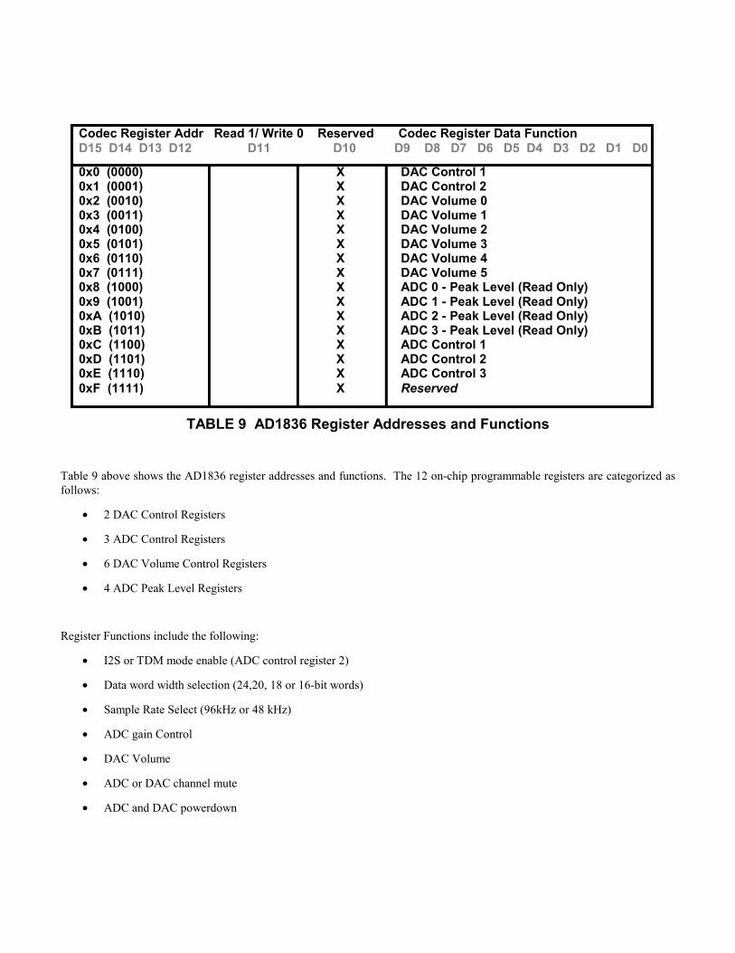
0x0 (0000) X DAC Control 1 0x1 (0001) X DAC Control 2 0x2 (0010) X DAC Volume 0 0x3 (0011) X DAC Volume 1 0x4 (0100) X DAC Volume 2 0x5 (0101) X DAC Volume 3 0x6 (0110) X DAC Volume 4 0x7 (0111) X DAC Volume 5 0x8 (1000) X ADC 0 - Peak Level (Read Only) 0x9 (1001) X ADC 1 - Peak Level (Read Only) 0xA (1010) X ADC 2 - Peak Level (Read Only) 0xB (1011) X ADC 3 - Peak Level (Read Only) 0xC (1100) X ADC Control 1 0xD (1101) X ADC Control 2 0xE (1110) X ADC Control 3 0xF (1111) X Reserved
Codec Register Addr Read 1/ Write 0 Reserved Codec Register Data Function D15 D14 D13 D12 D11 D10 D9 D8 D7 D6 D5 D4 D3 D2 D1 D0
TABLE 9 AD1836 Register Addresses and Functions
Table 9 above shows the AD1836 register addresses and functions. The 12 on-chip programmable registers are categorized as follows:
• 2 DAC Control Registers
• 3 ADC Control Registers
• 6 DAC Volume Control Registers
• 4 ADC Peak Level Registers
Register Functions include the following:
• I2S or TDM mode enable (ADC control register 2)
• Data word width selection (24,20, 18 or 16-bit words)
• Sample Rate Select (96kHz or 48 kHz)
• ADC gain Control
• DAC Volume
• ADC or DAC channel mute
• ADC and DAC powerdown

4.1 Configuring The AD1836 Serial Link To TDM Mode For ADI SPORT Compatibility The Extended TDM Mode allows an efficient communication interface between DSP and the AD1836. This mode of operation works efficiently with the use of serial port "autobuffering" or "DMA chaining." With this mode all 8 slots are 32-bits, allowing a simple interface to 32-bit DSPs like the ADSP-21161 with it's 32-bit serial shift registers. The DSP will generate a frame sync every 256 serial clock cycles.
8 x 32-bit timeslots = 256 bit clock cycles The DSP will generate a frame sync every 256 serial clock cycles. With an SCLK running at 12.288 MHz, the DSP will then produce the 48KHz frame sync. Please note that in Extended TDM mode, 96 kHz sampling rates are not supported. To take advantage of this feature, you must use I2S mode using up to 3 ADSP-21161 SPORTs (depending on the # of outputs required). By default, the AD1836 is in I2S mode. To initially configure the AD1836 to conform to DSP TDM schemes, the DSP should initially program the AD1836 for TDM mode as soon as the codec is operational (after a powerup reset or powerdown). #define SERIAL_CONFIGURATION 0x7400 #define ENABLE_Vfbit_SLOT1_SLOT2 0xE000 .var tx_buf[9] = ENABLE_Vfbit_SLOT1_SLOT2, /* set valid bits for slot 0, 1, and 2 */ SERIAL_CONFIGURATION, /* serial configuration register address 0x74 */ 0xFF80, /* initially set to SLOT-16 mode for ADI SPORT compatibility*/ 0x0000, /* stuff other slots with zeros for now */ 0x0000, 0x0000, 0x0000, 0x0000, 0x0000;
4.2 Programming the ADSP-21161 SPORT1/SPORT3 for "SPI Emulation" to
Communicate with the AD1836 SPI-Compatible Port The ADSP-21161 EZ-KIT lite allows the programming of the AD1836 registers via SPORT1 and SPORT3. This SPI emulation works well for the AD1836 extra clock requirement to latch data, because the SPORTs generate a continuous clock. The AD1836 does not care about a continous clock since the data is latched 1 cycle after the DSP's inverted frame sync goes high. To program the AD1836 registers, the SPORTs are programmed as follows:
SPORT3 Control Register (Configured as a transmitter)
• Late Frame Sync (Late FS3 and Active Low FS3 emulates the CLATCH operation) • Data Dependent Frame Sync • Internal Frame Sync • Internal SCLK3 • 16-bit words
SPORT1 Control Register (Configured as a receiver)
• Late Frame Sync • Active Low Frame Sync • External Frame Sync • External SCLK1 (tied together with SCLK3) • External FS1 (tied together with FS3) • 16-bit words

The ADSP-21161 assembly code instructions are shown below for configuring the SPORT1/SPORT3 pair for SPI emulation in order to provide the capability to program the AD1836 registers
/* clear multichannel/miscellaneous control register for SPORT1 & SPORT3 */ R0 = 0x0; dm(SP13MCTL) = R0; R0 = 0x0011002B; dm(DIV3) = R0; R0 = 0; dm(DIV1) = R0; bit set ustat1 DDIR | SDEN_A | LAFS | LFS | IFS | FSR | CKRE | ICLK | SLEN16 | SPEN_A;
dm(SPCTL3) = ustat1; bit set ustat2 SDEN_A | LAFS | LFS | FSR | CKRE | SLEN16 | SPEN_A; bit clr ustat2 DDIR | IFS | ICLK; dm(SPCTL1) = ustat2; bit set imask SP1I | SP3I; // enable SPORT1 RX and SPORT3 TX interrupts
4.3 Programming the ADSP-21161 SPI Master Port to Communicate with the AD1836
SPI-Compatible Port The ADSP-21161 EZ-KIT lite allows the programming of the AD1836 registers via the SPI port. This method will work with the next revision of AD1836 silicon, which will not have the extra clock requirement to latch data. To program the AD1836 registers via the SPI interface, the SPICTL register is programmed as follows:
SPICTL Register (Configured as a master SPI device)
• SPI Enable • Master SPI Device • SPI Transmit Interrupt Enable • Use FLAG0 as device select • CPHASE=1 • SPI Word Length = 16-bits • Baud Rate = 3.123 MHz • MSB first • Sign Extend
The ADSP-21161 assembly code instructions are shown below for configuring the SPI interface in order to provide the capability to program the AD1836 registers
bit set LIRPTL SPITMSK; // enable SPI TX interrupts bit set MODE1 IRPTEN; // allow global interrupts bit set IMASK LPISUMI; // unmask spi interrupts /* configure SPI port for interface to the AD1852 */ ustat1 = dm(SPICTL); bit set ustat1 SPIEN|SPTINT|TDMAEN|MS|FLS0|CPHASE|DF|WL16|BAUDR3|PSSE|DCPH0|SGN|GM; bit set ustat1 CP|FLS0|FLS2|FLS3|SMLS|DMISO|OPD|PACKEN|SENDZ|RDMAEN|SPRINT; dm(SPICTL) = ustat1; //enable SPI port
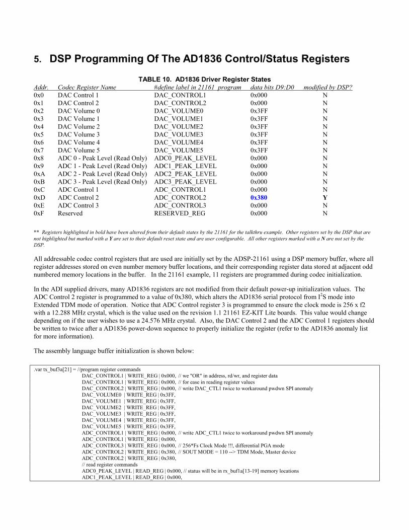
5. DSP Programming Of The AD1836 Control/Status Registers
TABLE 10. AD1836 Driver Register States Addr. Codec Register Name #define label in 21161 program data bits D9:D0 modified by DSP? 0x0 DAC Control 1 DAC_CONTROL1 0x000 N 0x1 DAC Control 2 DAC_CONTROL2 0x000 N 0x2 DAC Volume 0 DAC_VOLUME0 0x3FF N 0x3 DAC Volume 1 DAC_VOLUME1 0x3FF N 0x4 DAC Volume 2 DAC_VOLUME2 0x3FF N 0x5 DAC Volume 3 DAC_VOLUME3 0x3FF N 0x6 DAC Volume 4 DAC_VOLUME4 0x3FF N 0x7 DAC Volume 5 DAC_VOLUME5 0x3FF N 0x8 ADC 0 - Peak Level (Read Only) ADC0_PEAK_LEVEL 0x000 N 0x9 ADC 1 - Peak Level (Read Only) ADC1_PEAK_LEVEL 0x000 N 0xA ADC 2 - Peak Level (Read Only) ADC2_PEAK_LEVEL 0x000 N 0xB ADC 3 - Peak Level (Read Only) ADC3_PEAK_LEVEL 0x000 N 0xC ADC Control 1 ADC_CONTROL1 0x000 N 0xD ADC Control 2 ADC_CONTROL2 0x380 Y 0xE ADC Control 3 ADC_CONTROL3 0x000 N 0xF Reserved RESERVED_REG 0x000 N ** Registers highlighted in bold have been altered from their default states by the 21161 for the talkthru example. Other registers set by the DSP that are not highlighted but marked with a Y are set to their default reset state and are user configurable. All other registers marked with a N are not set by the DSP.
All addressable codec control registers that are used are initially set by the ADSP-21161 using a DSP memory buffer, where all register addresses stored on even number memory buffer locations, and their corresponding register data stored at adjacent odd numbered memory locations in the buffer. In the 21161 example, 11 registers are programmed during codec initialization.
In the ADI supplied drivers, many AD1836 registers are not modified from their default power-up initialization values. The ADC Control 2 register is programmed to a value of 0x380, which alters the AD1836 serial protocol from I2S mode into Extended TDM mode of operation. Notice that ADC Control register 3 is programmed to ensure the clock mode is 256 x f2 with a 12.288 MHz crystal, which is the value used on the revision 1.1 21161 EZ-KIT Lite boards. This value would change depending on if the user wishes to use a 24.576 MHz crystal. Also, the DAC Control 2 and the ADC Control 1 registers should be written to twice after a AD1836 power-down sequence to properly initialize the register (refer to the AD1836 anomaly list for more information).
The assembly language buffer initialization is shown below: .var tx_buf3a[21] = //program register commands DAC_CONTROL1 | WRITE_REG | 0x000, // we "OR" in address, rd/wr, and register data DAC_CONTROL1 | WRITE_REG | 0x000, // for ease in reading register values DAC_CONTROL2 | WRITE_REG | 0x000, // write DAC_CTL1 twice to workaround pwdwn SPI anomaly DAC_VOLUME0 | WRITE_REG | 0x3FF, DAC_VOLUME1 | WRITE_REG | 0x3FF, DAC_VOLUME2 | WRITE_REG | 0x3FF, DAC_VOLUME3 | WRITE_REG | 0x3FF, DAC_VOLUME4 | WRITE_REG | 0x3FF, DAC_VOLUME5 | WRITE_REG | 0x3FF, ADC_CONTROL1 | WRITE_REG | 0x000, // write ADC_CTL1 twice to workaround pwdwn SPI anomaly ADC_CONTROL1 | WRITE_REG | 0x000, ADC_CONTROL3 | WRITE_REG | 0x000, // 256*Fs Clock Mode !!!, differential PGA mode ADC_CONTROL2 | WRITE_REG | 0x380, // SOUT MODE = 110 --> TDM Mode, Master device ADC_CONTROL2 | WRITE_REG | 0x380, // read register commands ADC0_PEAK_LEVEL | READ_REG | 0x000, // status will be in rx_buf1a[13-19] memory locations ADC1_PEAK_LEVEL | READ_REG | 0x000,

ADC2_PEAK_LEVEL | READ_REG | 0x000, ADC3_PEAK_LEVEL | READ_REG | 0x000, ADC_CONTROL1 | READ_REG | 0x000, ADC_CONTROL2 | READ_REG | 0x000, ADC_CONTROL3 | READ_REG | 0x000; 5.1 Programming AD1836 Registers Using A Zero Overhead Loop Construct The following assembly language hardware DO LOOP shows how the values in the Init_Codec_Registers[ ] buffer are sent to the appropriate slots on the Serial Port TDM bus: /* Buffer holds SPI codes to write to each of 15 internal registers on 1836 */ .VAR Init_Codec_Registers[15] = DAC_CONTROL1 | WRITE_REG | 0x000, // we "OR" in address, rd/wr, and register data DAC_CONTROL1 | WRITE_REG | 0x000, // for ease in reading register values DAC_CONTROL2 | WRITE_REG | 0x000, // write DAC_CTL1 twice to workaround pwdwn SPI anomaly DAC_VOLUME0 | WRITE_REG | 0x3FF, DAC_VOLUME1 | WRITE_REG | 0x3FF, DAC_VOLUME2 | WRITE_REG | 0x3FF, DAC_VOLUME3 | WRITE_REG | 0x3FF, DAC_VOLUME4 | WRITE_REG | 0x3FF, DAC_VOLUME5 | WRITE_REG | 0x3FF, ADC_CONTROL1 | WRITE_REG | 0x000, // write ADC_CTL1 twice to workaround pwdwn SPI anomaly ADC_CONTROL1 | WRITE_REG | 0x000, ADC_CONTROL3 | WRITE_REG | 0x040, // 512*Fs Clock Mode !!!, differential PGA mode ADC_CONTROL2 | WRITE_REG | 0x380, // SOUT MODE = 110 --> TDM Mode, Master device ADC_CONTROL2 | WRITE_REG | 0x380; _______________________________________________ // Example Core-based loop via SPORT3 Program_AD1836_Registers: M7 = 1; I7 = Init_Codec_Registers; L7 = 0; lcntr = 15, DO Set_1836_Regs until LCE; r13 = dm(I7,M7); DM(TX3A) = r13; idle; Set_1836_Regs: nop; _______________________________________________ // Example Core-based loop via SPI Program_AD1836_Registers: M7 = 1; I7 = Init_Codec_Registers; L7 = 0; lcntr = 15, DO Set_1836_Regs until LCE; r13 = dm(I7,M7); DM(SPITX) = r13; idle;
Set_1836_Regs: nop; Explanation Of The AD1836 Codec Initialization Loop : • The buffer pointer is first set to point to the top of the codec register buffer. • The Loop Counter Register LCNTR is set to the number of registers to be programmed. In this case 11 registers are
programmed. • Memory writes to DM(TX3A) or DM(SPITX) will program the codec register address

• The IDLE instruction will tell the DSP to do nothing but wait for a SPORT3/SPI transmit interrupt after data has be written the the SPORT/SPI transmit buffer. Waiting for the SPORT/SPI interrupt will guarantee that all data in the transmit buffer has been shifted out on the serial bus, thus telling us it is safe to go the next codec register data value in the initialization buffer and place the word in the 'transmit buffer' queue.
5.2 Readback Of AD1836 Registers For Verification And Debugging Using A Zero-Overhead DO LOOP There are times over the debugging stage of driver code the DSP programmer may want to verify the desired values of the AD1836's internal registers. One easy way to do this is to set up an output buffer where all read requests of registers can be stored after codec initialization. The readback and status of codec registers can also be done using a hardware loop. The following assembly language instructions shown below are used to initiate codec read requests of registers shown in the Init_Codec_Registers[ ] buffer. The results of the read requests are then placed in an output buffer called Codec_Init_Results[. On the 2116 EZ-KIT Lite, the AD1836 registers can then be verified with JTAG emulator or the VDSP USB/JTAG debugger by setting a breakpoint after this section of code and opening up the memory window that shows the values stored in the memory buffer. After successful debugging of custom code these instructions can then be removed. /* Verify integrity of AD1836 register states to see if communication was successful */ verify_reg_writes: I7 = Init_Codec_Registers; M7 = 1; I5 = Codec_Init_Results; /////////////////////////// // SPORT1/3 version /////////////////////////// LCNTR = 15, Do ad1836_register_status UNTIL LCE; r13 = dm(I7,M7); DM(TX3A) = r13; idle; r3 = dm(RX1A); /* fetch value of requested indexed register data */ dm(I5,1) = r3; /* store to results buffer */ ad1836_register_status: nop; ___________________________________________ /////////////////////////// // SPI version /////////////////////////// lcntr = 15, DO Set_1836_Regs until LCE; r13 = dm(I7,M7); DM(SPITX) = r13; idle; r3 = dm(SPIRX); /* fetch value of requested indexed register data */ dm(I5,1) = r3; /* store to results buffer */ ad1836_register_status: nop;
Explanation Of The AD1836 Codec Register Readback Loop : • The buffer pointers I4 and I5 is first set to point to the top of the codec register buffer and codec results buffer. • The Loop Counter Register LCNTR is set to the number of registers to be read from the AD1836. • Memory writes from TX3A or SPITX will set a read request for the codec register address specified in the
Init_Codec_Registers[ ] buffer. • One IDLE instruction is required to correctly readback the codec after we transmit the request. • The pointer I5 copies the register address and data in the Codec_Init_Results[ ] buffer for every read request.

6. Processing AD1836 Audio Samples via the SPORT0 RX ISR In this section we investigate example DSP instructions for processing data from the SPORT0 receive interrupt vector. The ADSP-21161 typically processes newly received serial data by servicing SPORT interrupts, which redirects the program sequencer to jump to a SPORT interrupt vector, where it can then call the interrupt service routine. When using the SPORTs to process AD1836 TDM audio data samples, the application interrupt service routine code contain instructions which move audio data from a given input channel to that channels processing algorithm and places results back to any desired tx DMA buffer location, where it is shifted to the AD1836 where the data is converted back to an analog signal by the DACs. Figure 26 below shows a high level logical view of the audio streams that can be processed when interfacing the AD1836 to the SHARC DSP. With the AD1836's integrated stereo ADCs and DACs, each ADSP-21161 serial port TDM pair (SPORTs 0/2, 1/3) is capable of processing 8 input audio channels and send DSP output audio streams to 8 output channels. This type of configuration will allow implementation of a 8 x 2 channel digital mixing console, or provide a low cost solution for running surround algorithms requiring 8 channels for audio playback. With the use or both SPORT0 and SPORT2 in the TDM mode, the ADSP-21161 can interface to up to 2 AD1836s, resulting in an audio system with 16 audio input and output channels.
Figure 26. Logical View Of AD1836/SHARC Audio System
21161 EZ-KIT Lite's AD1836 Analog/Digital
Front End
ADSP-21161 Channel 1
Channel 2
Channel 3
Channel 4
Channel 5
Channel 6
Analog Stereo Inputs/Outputs
DSP Processing Routines
Channel 7
Channel 8
SP/DIF DAR
Analog Out 4 (AD1852 O/P)
Analog In1
Analog Out1
Analog In2
X (Unused)
Analog Out2
Analog Out3
In the reference AD1836 driver listed in Appendix A, the ADSP-21161’s SPORT0 Interrupt Vector/Interrupt Service Routine is used to process incoming information from the AD1836 through the serial port. As was described earlier in section 3.4, the information sent from the AD1836 is DMA-Chained (i.e., the SPORT receives the entire block of AD1836 audio frame data before a SPORT interrupt occurs, and the DMA parameter registers are automatically reloaded by the DSP's I/O processor to repeat the transfer of codec data) into the rx_buf0a[ ] buffer and an interrupt is generated when the rx buffer is filled with new data from the previously completed audio frame. Therefore, when a RX interrupt routine is being serviced the data from all active receive timeslots has been filled into the receive DMA buffer. When a TX interrupt routine is being services, the data from the tx DMA buffer has fully been transferred out to the serial port in the previously completed audio frame. Output left and right samples are filled into the transmit DMA buffer tx_buf2a[ ] for transmission out of SPORT. The programmer has the option of executing the DSP algorithm from either the transmit DMA interrupt or the receive DMA interrupt. Figure 27 shows the basic SPORT RX IRQ program flow structure for processing AD1836 audio data for the supplied DSP assembly and C drivers. This diagram shows the flow of audio samples from the serial port data buffer registers, to the DMA buffers, and from there, the audio samples are copied into temporary memory locations (double-buffered) to perform a "talkthru" of unprocessed audio streams, or to be used as inputs for the audio processing routines. The output data is then

copied from the output queue into the transmit DMA buffer, where it is then transferred to the SPORT transmit data register for shifting out of the serial port. The AD1836 codec processing instructions can be executed with either the transmit or receive interrupt.
SPORT0 TDM (ADC) Data
RX0A register
.VAR RX_BUF0a [8] RX0A DMA Buffer
DM Memory Variables(.VARs)
SPORT2 TDM (DAC)Data
DSP Audio Algorithm Routines
+ AUX_ADC_L0
+ Internal_ADC_L1
+ Internal_ADC_R0
+ AUX_ADC_R0
Left_Channel_SPDIF_rx
Right_Channel_In0
Right_Channel_In1
Right_Channel_SPDIF_rx
TX2A register
.VAR TX_BUF2a [8] TX2A DMA Buffer
+ Internal_DAC_L2
+ Internal_DAC_R0
+ Internal_DAC_R1
+ Internal_DAC_R2
tx_buf2a+ Internal_DAC_L0
+ Internal_DAC_L1 DMA transfer from
Internal Memory
Left_Channel_Out2
Right_Channel_Out0 Right_Channel_Out1 Right_Channel_Out2
Left_Channel_Out0 Left_Channel_Out1
Left_Channel_In1
Left_Channel_In0 + Internal_ADC_L0
rx_buf0a + Internal_ADC_L0 DMA transfer to
Internal Memory
RX0A DMA Interrupt Generated when RX_BUF0a fills up with new AD1836 audio samples. The data is quickly saved to variables in memory for audio processing
SPORT0 RX ISR Flow
+ AUX_DAC_L0
+ AUX_DAC_R0
Left_Channel_AD1852
Right_Channel_AD1852
Fig 27. SPORT 0 RX Interrupt Service Routine Data Flow Structure for AD1836 Audio Processing
SPORT0 RX Interrupt Service Routine Workflow
1) Get new audio samples received from AD1836 via the SPORT receive DMA buffer rx_buf0a[ ] . 2) Save new audio samples to Audio Variables in Memory for DSP Processing 6) Run Desired DSP Algorithm 4) Retrieve processed audio samples from Audio Variables in Memory 7) Copy DSP Algorithm Results to AD1836 DACs via the SPORT DMA buffer tx_buf2a[ ] .

Notice that the AD1836 reference driver code copies all incoming data from the SPORT receive DMA buffer into temporary DSP memory locations, or variables. Once audio data is processed by the ADSP-21161, the results are copied into temporary output variables in DSP memory memory, where it will be read by the SPORT0 interrupt service routine and copied into the output transmit DMA buffer. Notice that all Analog Devices supplied EZ-KIT assembly and C demos use the same standard names for input and output audio variables. The following Table 11 shows the definitions for these variables in both assembly and C and how they are related to the DMA transmit and receive buffer offsets:
TABLE11. DMA Buffer relationship to Data Memory Audio Variables
Timeslot # SPORT DMA Buffer Timeslot Data = Temp Audio Variable Equivalent 0 DM(rx_buf0a + Internal_ADC_L0) DM(Left_Channel_In0) 1 DM(rx_buf0a + Internal_ADC_L1) DM(Left_Channel_In1) 2 DM(rx_buf0a + AUX_ADC_L0) DM(Left_Channel_SPDIF_rx) 3 DM(rx_buf0a + AUX_ADC_L1) X (not used in EZ-KIT Lite) 4 DM(rx_buf0a + Internal_ADC_R0) DM(Right_Channel_In0) 5 DM(rx_buf0a + Internal_ADC_R1) DM(Right_Channel_In1) 6 DM(rx_buf0a + AUX_ADC_R0) DM(Left_Channel_SPDIF_rx) 7 DM(rx_buf0a + AUX_ADC_R0) X (not used in EZ-KIT Lite) 0 DM(tx_buf2a + Internal_DAC_L0) DM(Left_Channel_Out0) 1 DM(tx_buf2a + Internal_DAC_L1) DM(Left_Channel_Out1) 2 DM(tx_buf2a + Internal_DAC_L2) DM(Left_Channel_Out2) 3 DM(tx_buf2a + AUX_DAC_L0) DM(Left_Channel_AD1852) 4 DM(tx_buf2a + Internal_DAC_R0) DM(Right_Channel_Out0) 5 DM(tx_buf2a + Internal_DAC_R1) DM(Right_Channel_Out1) 6 DM(tx_buf2a + Internal_DAC_R2) DM(Right_Channel_Out2) 7 DM(tx_buf2a + AUX_DAC_R0) DM(Right_Channel_AD1852) Assembly Variable Declarations .segment /dm dm_codec; /* AD1836 stereo-channel data holders - used for DSP processing of audio data received from codec */ .VAR Left_Channel_In0; /* Input values from AD1836 ADCs */ .VAR Left_Channel_In1; .VAR Right_Channel_In0; .VAR Right_Channel_In1; .VAR Left_Channel_SPDIF_rx; .VAR Right_Channel_SPDIF_rx; .VAR Left_Channel_Out0; /* Output values for AD1836 DACs */ .VAR Left_Channel_Out1; .VAR Left_Channel_Out2; .VAR Right_Channel_Out0; .VAR Right_Channel_Out1; .VAR Right_Channel_Out2; .VAR Left_Channel_AD1852; .VAR Right_Channel_AD1852; .VAR Left_Channel; /* can use for intermediate results to next filter stage */ .VAR Right_Channel; /* can use for intermediate results to next filter stage */ .endseg;

C-Style Variable Declarations C-Callable Assembly Variable Declarations in ADDS_21161_EZKIT.ASM /* AD1836 stereo-channel data holders - used for DSP processing of audio data received from codec */ // input channels .var _Left_Channel_In0; /* Input values from the 2 AD1836 internal stereo ADCs */ .var _Left_Channel_In1; /* 1/8th inch stereo jack connected to internal stereo ADC1 */ .var _Right_Channel_In0; .var _Right_Channel_In1; .var _Left_Channel_SPDIF_rx; /* Input values from the DAR CS8414 */ .var _Right_Channel_SPDIF_rx; //output channels .var _Left_Channel_Out0; /* Output values for the 3 AD1836 internal stereo DACs */ .var _Left_Channel_Out1; /* Left and Right Channel 0 DACs go to headphone jack */ .var _Left_Channel_Out2; .var _Right_Channel_Out0; .var _Right_Channel_Out1; .var _Right_Channel_Out2; .var _Left_Channel_AD1852; /* Output values for AD1852 stereo DAC */ .var _Right_Channel_AD1852; Equivalent External C Definitions in ADDS_21161_EZKIT.H // input channels extern int Left_Channel_In0; /* Input values from the 2 AD1836 internal stereo ADCs */ extern int Left_Channel_In1; /* 1/8th inch stereo jack connected to internal stereo ADC1 */ extern int Right_Channel_In0; extern int Right_Channel_In1; extern int Left_Channel_SPDIF_rx; /* Input values from the DAR CS8414 */ extern int Right_Channel_SPDIF_rx; //output channels extern int Left_Channel_Out0; /* Output values for the 3 AD1836 internal stereo DACs */ extern int Left_Channel_Out1; /* Left and Right Channel 0 DACs go to headphone jack */ extern int Left_Channel_Out2; extern int Right_Channel_Out0; extern int Right_Channel_Out1; extern int Right_Channel_Out2; extern int Left_Channel_AD1852; /* Output values for AD1852 stereo DAC */ extern int Right_Channel_AD1852;

6.1 ADSP-21161 SPORT DMA & AD1836 Multichannel Timing Notes Depending on processing data from the SPORT2 transmit interrupt or SPORT0 receive interrupt, the DSP programmer should be aware of TX/RX serial interrupt timing differences. If we process data from the SPORT2 transmit interrupt, the DSP will process incoming rx data in the current frame for timeslots 0 to 5. However, current audio frame timeslots 6 and 7 may not be processed until the received audio frame or next transmit interrupt. Similarly, if we process data using the SPORT0 receive interrupt, tx DMA data for timeslots 0 and 1 have already been transferred from the transmit DMA buffers into the SPORT tx FIFO "queue", so the newly processed data for slots 0 and 1 will not be transmitted until the next audio frame. The reason for this difference is because when using SPORT TX and RX DMA chaining in TDM mode, the DMA interrupts are always at least two timeslots apart (See Figure 28 below). This is because the Transmit TCB initially places the first two words from the tx DMA buffer into the SPORT1 TX buffer registers. This automatically decrements the Transmit DMA count register by two. After the assertion of the TX chained-DMA interrupt, the data for channels 6 and 7 have not been DMA'ed into internal memory yet. Thus, before timeslot 0 even begins transmit/receive activity, the RX DMA Count = 8 while the TX DMA Count = 6 (assuming we have declared 8-word TX and RX DMA buffers with 8 active timeslots enabled on the serial port). The transmit interrupt occurs when the TX DMA Count = 0, and this interrupt request occurs on the second DSP clock cycle immediately after the LSB of timeslot 5 is transmitted. While this transmit interrupt is generated, the transmit data for the AD1836 right channel DAC3 timeslot is currently shifting out of the SPORT's Tx-shift register in slot 6, while the AD1836 right auxiliary DAC channel (AD1852 right) data for channel 7 is in the TX2A register queue, waiting to be transmitted after timeslot 6 data is finished shifting out of the SPORT. After both the transmit and receive interrupts are latched in the current frame [after timeslots 5(tx) or 7(rx)], the TCBs will be reloaded, and then DMA internal memory transfers will.
Figure 28. AD1836/SPORT Timeslot, DMA Count and RX & TX Interrupt Timing Relationships __ __ FSTDM ___| |_________________________________________________________________________| |_
D0A < SLOT0 >< SLOT1 >< SLOT2 >< SLOT3 >< SLOT4 >< SLOT5 >< SLOT6 >< SLOT7 >
C0A 8 7 6 5 4 3 2 1 0 RX IRQ Here (DMA RX Count Reg)
D2A < SLOT0 >< SLOT1 >< SLOT2 >< SLOT3 >< SLOT4 >< SLOT5 >< SLOT6 >< SLOT7 > C3A 6 5 4 3 2 1 0 TX IRQ Here (DMA TX Count Reg) [TX queue reloaded with 1st two tx_buf values after TCB download as slots 6 and 7 are shifted out of SPORT1]
(1 / 12.288 MHz SCLK) x (32-bits/timeslot) x (2 timeslots) = 5.208 microseconds
1 / 100 MHz Instruction Execution = 10 nanoseconds per instruction
5.208 microseconds / 10 nanoseconds = 156.25 = 521 DSP CCLK cycles TX/RX DMA IRQ difference
These DMA timing differences are important to know, however they are not catastrophic for the DSP system designer. Since the AD1836 does not contain control, register or valid tag information on timeslot like AC-97 codecs (which are severely affected by these DMA timing differences), the audio frame latency issues for the AD1836 are not a problem, since user's cannot perceive an audio delay of one 48 KHz sample between the input from the AD1836 to SPORT0, and the output of SPORT2 to the AD1836.

6.2 Multichannel, DMA and ISR Methods of Implementation For Processing 48 kHz Data Now that we have examined in section 6.1 the relative timing difference in SPORT TX and RX interrupts between the transmit and receive channels, we will investigate a SPORT0 receive interrupt implementation methods to process all audio streams to/from the AD1836. In certain applications, the user may want to process codec data elsewhere. For example, in C-based applications, the C-runtime DSP routines may be placed in a main program 'while' loop waiting for SPORT interrupts. The codec interrupt service routine's responsibility would be to receive and transmit codec data, while the processing of the data is done elsewhere. For example, the ADSP-21161 EZ-KIT Lite demos examples use a double buffering scheme, which allows the user to copy data into a temporary buffer, such that while the DMA buffers are currently being filled, the user processed data from alternate background buffers. After audio data is processed, the information is copied to the transmit user buffer. To prepare DAC data to transmit in the next audio frame, the DSP's SPORT ISR instructions should simply include DM data transfers the appropriate locations in the SPORT transmit DMA buffer, which in turn is transferred out of the serial port on the next TDM frame sync assertion. The DSP's SPORT interrupt routine then executes instructions to ensure that it will place processed data in the left channel slots (slot 0, slot1, slot2, slot3) and the right channel slots (slot4, slot5, slot6, slot7). This single sample processing method is more of a pipelined FIFO approach, in which we always will transmit the newly processed sample to the DACs in the next audio frame every time we get the new ADC sample and process it. Let's look at the ADSP-21161 Assembly Language Instructions that are incorporated in our 21161 codec SPORT0 Interrupt Service Routine (in Appendix A) that demonstrate how we process the audio data. 1) The following instructions demonstrate how to copy new AD1836 ADC data for all incoming timeslots and save our current left and right channel data for processing (this "double buffers" the incoming data so that it does not get overwritten by current SPORT DMA receive operations when executing larger algorithms): Process_AD1836_Audio_Samples: /* get AD1836 left channel input samples, save to data holders for processing */ r0 = dm(rx0a_buf + Internal_ADC_L0); dm(Left_Channel_In0) = r0; r0 = dm(rx0a_buf + Internal_ADC_L1); dm(Left_Channel_In1) = r0; r0 = dm(rx0a_buf + AUX_ADC_L0); dm(Left_Channel_SPDIF_rx) = r r0; /* get AD1836 right channel input samples, save to data holders for processing */ r0 = dm(rx0a_buf + Internal_ADC_R0); dm(Right_Channel_In0) = r0; r0 = dm(rx0a_buf + Internal_ADC_R1); dm(Right_Channel_In1) = r0; r0 = dm(rx0a_buf + AUX_ADC_R0); dm(Right_Channel_SPDIF_rx) = r0;
2) We then call our DSP algorithm: do_audio_processing: call (pc, process_audio);
3) After processing our incoming ADC data, we send our processed results to the AD1836 DACs in the next audio frame. To accomplish this, we simply copy our results from our output audio variables and place them in the SPORT tx DMA "queue" in tx_buf2a[ ]. /* ---- DSP processing is finished, now playback results to AD1836 ---- */ playback_AD1836_left_DACs: /* output processed left ch audio samples to AD1836 */ r0 = dm(Left_Channel_Out0); dm(tx2a_buf + Internal_DAC_L0) = r0; r1 = dm(Left_Channel_Out1); dm(tx2a_buf + Internal_DAC_L1) = r1; r2 = dm(Left_Channel_Out2); dm(tx2a_buf + Internal_DAC_L2) = r2; r3 = dm(Left_Channel_AD1852); dm(tx2a_buf + AUX_DAC_L0) = r3; playback_AD1836_right_DACs: /* output processed right ch audio samples to AD1836 */ r0 = dm(Right_Channel_Out0); dm(tx2a_buf + Internal_DAC_R0) = r0; r1 = dm(Right_Channel_Out1); dm(tx2a_buf + Internal_DAC_R1) = r1; r2 = dm(Right_Channel_Out2); dm(tx2a_buf + Internal_DAC_R2) = r2; r3 = dm(Right_Channel_AD1852); dm(tx2a_buf + AUX_DAC_R0) = r3;

6.3 Processing 24-bit Data In 1.31 Fractional Format Or IEEE 32-bit Floating Point Format Data that is received or transmitted in the SPORT1 ISR is in a binary, 2's complement format. The DSP interprets the data in fractional format, where all #s are between -1 and 0.9999999. Initially, the serial port places the data into internal memory in data bits D0 to D15. In order to process the fractional data in 1.31 format, the AD1836 left justifies the 24-bit data to the upper 32-bits of the timeslot data-word. This makes it simple to take advantage of the fixed-point multiply/accumulator's fractional 1.31 mode, as well as offer an easy reference for converting from 1.31 fractional to floating point formats. This also guarantees that any quantization errors resulting from the computations will remain well below the 24-bit result and thus below the AD1836 DACs' 105 dB Noise Floor. After processing the data, the 1.31 fractional result is then sent to the AD1836, where the AD1836 will truncate the 32-bit dataword to 24-bits before DAC conversion. Below are example instructions to demonstrate shifting of data before and after the processing of data on the Master AD1836 left channel: 32-bit Fixed Point Processing r1 = dm(rx_buf0a + Internal_ADC_L0); /* get AD1836 left channel ADC0 input sample */ dm(Left_Channel_In0)=r1; /* save to data holder for processing */ /* Process data here, data is processed in 1.31 format */ [Call Fixed_Point_Algorithm] r15 = dm(Left_Channel_Out0); /* get channel 1 output result */ dm(tx_buf2a + Internal_DAC_L0) = r15; /* output left result to AD1836 left channel DAC0 */ 32-bit Floating Point Processing To convert between our assumed 1.31 fractional number and IEEE floating point math, here are some example assembly instructions. This assumes that our AD1836 data has already been converted to floating point format, as shown above: r1 = -31; <-- scale the sample to the range of +/-1.0 r0 = DM(Left_Channel_In0); f0 = float r0 by r1; [Call Floating_Point_Algorithm] r1 = 31; <-- scale the result back up to MSBs r8 = fix f8 by r1; DM(Left_Channel_Out0) = r8;
REFERENCES The following sources contributed information to this applications note:
[1] L. D. Fielder, "Human Auditory Capabilities and Their Consequences in Digital-Audio Converter Design", Audio in Digital Times, Proc. Audio En g. Soc. 7th Inter. Conf., Toronto, Ont., Canada, May 14th-17th 1989, pp. 45-62. [2] Analog Devices Whitepaper, ADSP-21065L: Low-Cost 32-bit Processing for High Fidelity Digital Audio, Analog Devices, 3 Technology Way, Norwood, MA, November 1997 [3] R. Wilson, “Filter Topologies”, J. Audio Engineering Society, Vol 41, No. 9, September 1993 [4] J. Dattorro, “The Implementation of Digital Filters for High Fidelity Audio”, Audio in Digital Times, Proc. Audio En g. Soc. 7th Inter. Conf., Toronto, Ont., Canada, May 14th-17th 1989, pp. 165-180. [5] Udo Zolzer, “Roundoff Error Analysis of Digital Filters”, J. Audio Engineering Society, Vol42, No. 4, April 1994 [6] K. L. Kloker, B. L. Lindsley, C.D. Thompson, “VLSI Architectures for Digital Audio Signal Processing,” Audio in Digital Times, Proc. Audio En g. Soc. 7th Inter. Conf., Toronto, Ont., Canada, May 14th-17th 1989, pp. 313-325 [7] Chen, C, “Performance of Cascade and Parallel IIR Filters,” Jour Audio Eng Soc, March 1996, Vol 44, No 3. [11] Gary Davis & Ralph Jones, Sound Reinforcement Handbook, 2nd Edition”, Ch. 14, pp. 259-278, Yamaha Corporation of America, (1989, 1990) 8] ADSP-21161 SHARC DSP Hardware Reference Manual, Second Edition, June 2001, Analog Devices, Inc., (82-001944-02) [9] AD1836 Data Sheet, Analog Devices, Inc,.
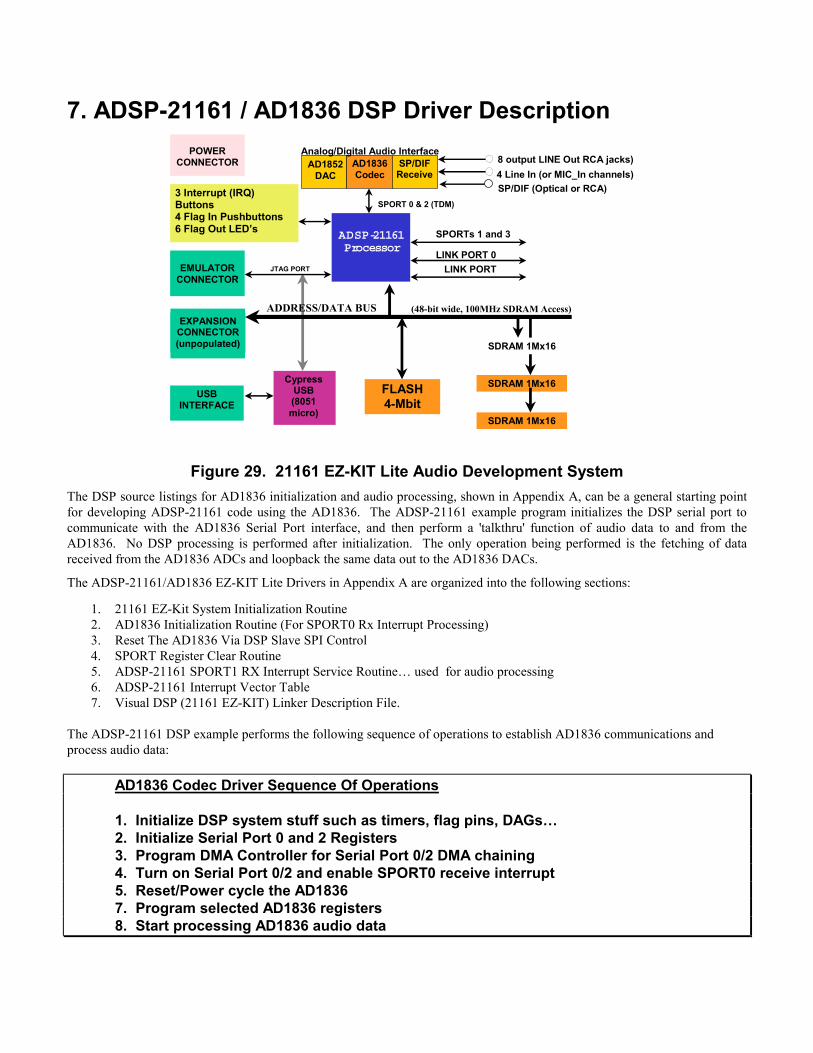
7. ADSP-21161 / AD1836 DSP Driver Description
EMULATOR CONNECTOR
EXPANSION CONNECTOR (unpopulated)
FLASH 4-Mbit
USB INTERFACE
8 output LINE Out RCA jacks)
SPORTs 1 and 3
JTAG PORT
4 Line In (or MIC_In channels)
(48-bit wide, 100MHz SDRAM Access)
SPORT 0 & 2 (TDM)
Cypress USB (8051 micro)
POWER CONNECTOR
3 Interrupt (IRQ) Buttons 4 Flag In Pushbuttons 6 Flag Out LED’s
SDRAM 1Mx16
SDRAM 1Mx16
ADSP-21161 Processor
LINK PORT
LINK PORT 0
SDRAM 1Mx16
SP/DIF (Optical or RCA)
ADDRESS/DATA BUS
AD1852 DAC
AD1836 Codec
Analog/Digital Audio Interface SP/DIF
Receive
Figure 29. 21161 EZ-KIT Lite Audio Development System
The DSP source listings for AD1836 initialization and audio processing, shown in Appendix A, can be a general starting point for developing ADSP-21161 code using the AD1836. The ADSP-21161 example program initializes the DSP serial port to communicate with the AD1836 Serial Port interface, and then perform a 'talkthru' function of audio data to and from the AD1836. No DSP processing is performed after initialization. The only operation being performed is the fetching of data received from the AD1836 ADCs and loopback the same data out to the AD1836 DACs.
The ADSP-21161/AD1836 EZ-KIT Lite Drivers in Appendix A are organized into the following sections:
1. 21161 EZ-Kit System Initialization Routine 2. AD1836 Initialization Routine (For SPORT0 Rx Interrupt Processing) 3. Reset The AD1836 Via DSP Slave SPI Control 4. SPORT Register Clear Routine 5. ADSP-21161 SPORT1 RX Interrupt Service Routine… used for audio processing 6. ADSP-21161 Interrupt Vector Table 7. Visual DSP (21161 EZ-KIT) Linker Description File.
The ADSP-21161 DSP example performs the following sequence of operations to establish AD1836 communications and process audio data:
AD1836 Codec Driver Sequence Of Operations 1. Initialize DSP system stuff such as timers, flag pins, DAGs… 2. Initialize Serial Port 0 and 2 Registers 3. Program DMA Controller for Serial Port 0/2 DMA chaining 4. Turn on Serial Port 0/2 and enable SPORT0 receive interrupt
5. Reset/Power cycle the AD1836 7. Program selected AD1836 registers
8. Start processing AD1836 audio data

APPENDIX A: Assembly Source Code Listing for 21161 EZ-KIT Lite Audio Driver (Visual DSP Project Files) 21161 EZ-KIT System Initialization Routine /*** INIT_21161_EZKIT.ASM *************************************************** * * * ADSP-21161 EZ-KIT Initialization and Main Program Shell * * Developed using the ADSP-21161 EZ-KIT LIte Evaluation Platform * * * * * * John Tomarakos * * ADI DSP Applications Group * * Revision 1.0 * * 1/30/01 * * * *********************************************************************************/ /* ADSP-21161 System Register bit definitions */ #include "def21161.h" .GLOBAL _main; .GLOBAL Init_DSP; //.EXTERN init_21161_SDRAM_controller; //.EXTERN Program_SPORT02_TDM_Registers; //.EXTERN Program_AD1836_regs_via_SPI; //.EXTERN Program_SPORT02_DMA_Channels; //.EXTERN AD1836_Codec_Initialization; //.EXTERN Init_AD1852_DACs; //.EXTERN Reg_SPI_Code_init; //.EXTERN Clear_All_SPT_Regs; //.EXTERN user_code_init; /*---------------------------------------------------------------------------*/ .section /pm pm_code; _main: /* This may be required for disabling SPORT config for EZLAB debugger */ CALL Clear_All_SPT_Regs; /* Clear and Reset SPORTs and DMAs */ call init_21161_SDRAM_controller; /* Initialize External Memory */ call Program_AD1836_regs_via_SPI; /* Use SPORTs 1&3 to talk to AD1836 SPI interface */ /* and program AD1836 Registers*/ call Init_AD1852_DACs; call Program_SPORT02_TDM_Registers; /* Initialize SPORTs for codec communications */ call Program_SPORT02_DMA_Channels; /* Start Serial Port 1 tx and rx DMA Transfers */ call user_code_init; /* initialize user buffers */ IRPTL = 0x00000000; /* clear pending interrupts */ bit set imask SP0I|SP2I; /* start audio processing, enable SPORT1 tx & rx int */ bit set imask IRQ0I | IRQ1I | IRQ2I; /* irq0, irq1 and irq2 enabled */ ustat2 = dm(SP02MCTL); bit set ustat2 MCE; dm(SP02MCTL) = ustat2; call Blink_LEDs_Test; /* Are We Alive? */ wait_forever: /* wait forever loop */ idle; jump wait_forever; /*--------------------------------------------------------------------------------------*/ /* Note: This routine is first called at the Reset Vector in the Interrupt Vector Table */ /*--------------------------------------------------------------------------------------*/
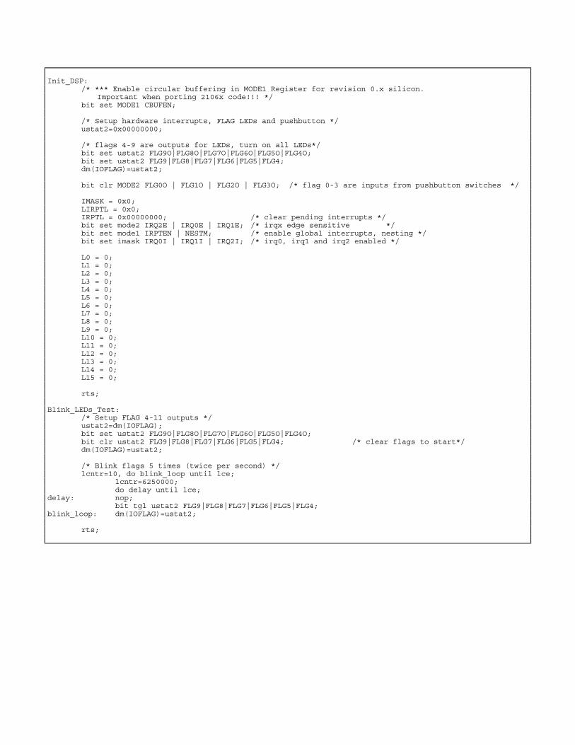
Init_DSP: /* *** Enable circular buffering in MODE1 Register for revision 0.x silicon. Important when porting 2106x code!!! */ bit set MODE1 CBUFEN; /* Setup hardware interrupts, FLAG LEDs and pushbutton */ ustat2=0x00000000; /* flags 4-9 are outputs for LEDs, turn on all LEDs*/ bit set ustat2 FLG9O|FLG8O|FLG7O|FLG6O|FLG5O|FLG4O; bit set ustat2 FLG9|FLG8|FLG7|FLG6|FLG5|FLG4; dm(IOFLAG)=ustat2; bit clr MODE2 FLG0O | FLG1O | FLG2O | FLG3O; /* flag 0-3 are inputs from pushbutton switches */ IMASK = 0x0; LIRPTL = 0x0; IRPTL = 0x00000000; /* clear pending interrupts */ bit set mode2 IRQ2E | IRQ0E | IRQ1E; /* irqx edge sensitive */ bit set mode1 IRPTEN | NESTM; /* enable global interrupts, nesting */ bit set imask IRQ0I | IRQ1I | IRQ2I; /* irq0, irq1 and irq2 enabled */ L0 = 0; L1 = 0; L2 = 0; L3 = 0; L4 = 0; L5 = 0; L6 = 0; L7 = 0; L8 = 0; L9 = 0; L10 = 0; L11 = 0; L12 = 0; L13 = 0; L14 = 0; L15 = 0; rts; Blink_LEDs_Test: /* Setup FLAG 4-11 outputs */ ustat2=dm(IOFLAG); bit set ustat2 FLG9O|FLG8O|FLG7O|FLG6O|FLG5O|FLG4O; bit clr ustat2 FLG9|FLG8|FLG7|FLG6|FLG5|FLG4; /* clear flags to start*/ dm(IOFLAG)=ustat2; /* Blink flags 5 times (twice per second) */ lcntr=10, do blink_loop until lce; lcntr=6250000; do delay until lce; delay: nop; bit tgl ustat2 FLG9|FLG8|FLG7|FLG6|FLG5|FLG4; blink_loop: dm(IOFLAG)=ustat2; rts;

AD1836 Initialization Routine /*** SPORTs1&3_SPI_Emulation.ASM ******************************************** * * * AD1836/ADSP-21161 SPI Code Register Initialization via SPI Emulation * * * * John Tomarakos * * ADI DSP Applications Group * * Revision 2.0 * * 03/05/01 * * * *********************************************************************************/ /* ADSP-21161 System Register bit definitions */ /* refer to latest DEF21161.H file for SPORT bitfield definitions */ #include "def21161.h" .GLOBAL Program_AD1836_regs_via_SPI; .GLOBAL Count_SPORT1_RX_IRQs; .GLOBAL Count_SPORT3_TX_IRQs; //.EXTERN Wait_Approx_999us; .GLOBAL Wait_Approx_1500ms; .GLOBAL Wait_Approx_167ms; // AD1836 codec SPI control/status register definitions #define READ_REG 0x0800 #define WRITE_REG 0x0000 #define DAC_CONTROL1 0x0000 #define DAC_CONTROL2 0x1000 #define DAC_VOLUME0 0x2000 #define DAC_VOLUME1 0x3000 #define DAC_VOLUME2 0x4000 #define DAC_VOLUME3 0x5000 #define DAC_VOLUME4 0x6000 #define DAC_VOLUME5 0x7000 #define ADC0_PEAK_LEVEL 0x8000 #define ADC1_PEAK_LEVEL 0x9000 #define ADC2_PEAK_LEVEL 0xA000 #define ADC3_PEAK_LEVEL 0xB000 #define ADC_CONTROL1 0xC000 #define ADC_CONTROL2 0xD000 #define ADC_CONTROL3 0xE000 #define RESERVED_REG 0xF000 .section/dm dm_data; /* Powerdown ADCs and DACs twice to get around AD1836 SPI/powerdown anomaly */ .var powerdown_AD1836[4] = DAC_CONTROL1 | WRITE_REG | 0x004, DAC_CONTROL1 | WRITE_REG | 0x004, ADC_CONTROL1 | WRITE_REG | 0x080, ADC_CONTROL1 | WRITE_REG | 0x080; .var powerdown_rx_buf0a[4]; // rx dma dummy buffer not used for anything; // AD1836 codec register commands - Serial SPI 16-bit Word Format as follows: // D15 to D12 = Codec Register Address // D11 = Read/Write register (1=rd, 0=wr) // D10 = reserved bit, clear to zero // D9 to D0 = Data Field for codec register .var tx_buf3a[21] = //program register commands DAC_CONTROL1 | WRITE_REG | 0x000, // we "OR" in address, rd/wr, and register data DAC_CONTROL1 | WRITE_REG | 0x000, // for ease in reading register values DAC_CONTROL2 | WRITE_REG | 0x000, // write DAC_CTL1 twice to workaround pwdwn SPI anomaly DAC_VOLUME0 | WRITE_REG | 0x3FF, DAC_VOLUME1 | WRITE_REG | 0x3FF, DAC_VOLUME2 | WRITE_REG | 0x3FF, DAC_VOLUME3 | WRITE_REG | 0x3FF, DAC_VOLUME4 | WRITE_REG | 0x3FF, DAC_VOLUME5 | WRITE_REG | 0x3FF, ADC_CONTROL1 | WRITE_REG | 0x000, // write ADC_CTL1 twice to workaround pwdwn SPI anomaly ADC_CONTROL1 | WRITE_REG | 0x000, ADC_CONTROL3 | WRITE_REG | 0x000, // 256*Fs Clock Mode !!!, differential PGA mode ADC_CONTROL2 | WRITE_REG | 0x380, // SOUT MODE = 110 --> TDM Mode, Master device

ADC_CONTROL2 | WRITE_REG | 0x380, // read register commands ADC0_PEAK_LEVEL | READ_REG | 0x000, // status will be in rx_buf1a[13-19] memory locations ADC1_PEAK_LEVEL | READ_REG | 0x000, ADC2_PEAK_LEVEL | READ_REG | 0x000, ADC3_PEAK_LEVEL | READ_REG | 0x000, ADC_CONTROL1 | READ_REG | 0x000, ADC_CONTROL2 | READ_REG | 0x000, ADC_CONTROL3 | READ_REG | 0x000; .var rx_buf1a[21]; /* ISR counters, for debug purposes to see how many times SPORT DMA interrupts are serviced */ .VAR SP1I_counter = 0; .VAR SP3I_counter = 0; .section /pm pm_code; ///////////////////////////////////////////////////////////////////////////////////////// // // // Program SPORT1 & SPORT3 Control Registers for SPI emulation control // // // ///////////////////////////////////////////////////////////////////////////////////////// Program_AD1836_regs_via_SPI: r0=0x00000000; // initially clear SPORT control register dm(SPCTL1)=r0; dm(SPCTL3)=r0; ustat1=dm(SPCTL3); ustat2=dm(SPCTL1); ustat3=dm(SP13MCTL); powerdown_reset_AD1836: r0=powerdown_AD1836; dm(II3A)=r0; /* Internal DMA6 memory address */ r0=1; dm(IM3A)=r0; /* Internal DMA6 memory access modifier */ r0=@powerdown_AD1836; dm(C3A)=r0; /* Contains number of DMA6 transfers to be done */ r0=powerdown_rx_buf0a; dm(II1A)=r0; /* Internal DMA2 memory address */ r0=1; dm(IM1A)=r0; /* Internal DMA2 memory access modifier */ r0=@powerdown_rx_buf0a; dm(C1A)=r0; /* Contains number of DMA2 transfers to be done */ /* clear multichannel/miscellaneous control register for SPORT1 & SPORT3 */ R0 = 0x0; dm(SP13MCTL) = R0; R0 = 0x0011002B; dm(DIV3) = R0; R0 = 0; dm(DIV1) = R0; bit set ustat1 DDIR | SDEN_A | LAFS | LFS | IFS | FSR | CKRE | ICLK | SLEN16 | SPEN_A; dm(SPCTL3) = ustat1; bit set ustat2 SDEN_A | LAFS | LFS | FSR | CKRE | SLEN16 | SPEN_A; bit clr ustat2 DDIR | IFS | ICLK; dm(SPCTL1) = ustat2; bit set imask SP1I | SP3I; // enable SPORT1 RX and SPORT3 TX interrupts powerdwm_not_done_yet: idle; R1 = 0x00000008; // Test for SPORT3 R0 = DM(DMASTAT); R0 = R0 AND R1; IF NE jump powerdwm_not_done_yet; bit clr imask SP1I|SP3I; // disable SPORT1 RX and SPORT3 TX interrupts Wait_Approx_1s: lcntr = 3000, do waitloop until lce; nop; nop; nop; waitloop: nop; bit clr ustat1 0xFFFFFFFF; dm(SPCTL1) = ustat1; dm(SPCTL3) = ustat1; IRPTL=0;

bit clr IMASK SP1I | SP3I; SPORT_DMA_setup: r0=0x00000000; // initially clear SPORT control register dm(SPCTL1)=r0; dm(SPCTL3)=r0; ustat1=dm(SPCTL3); ustat2=dm(SPCTL1); ustat3=dm(SP13MCTL); r0=tx_buf3a; dm(II3A)=r0; /* Internal DMA6 memory address */ r0=1; dm(IM3A)=r0; /* Internal DMA6 memory access modifier */ r0=@tx_buf3a; dm(C3A)=r0; /* Contains number of DMA6 transfers to be done */ r0=rx_buf1a; dm(II1A)=r0; /* Internal DMA2 memory address */ r0=1; dm(IM1A)=r0; /* Internal DMA2 memory access modifier */ r0=@rx_buf1a; dm(C1A)=r0; /* Contains number of DMA2 transfers to be done */ /* clear multichannel/miscellaneous control register for SPORT1 & SPORT3 */ R0 = 0x0; dm(SP13MCTL) = R0; /*internally generating FS3 and *HARDWARE* loop it back to FS1 for SPORT1/3 SPI control*/
/* Maximum SPI serial bit clock rate is 8MHz... select 1 MHz to allow safety factor of 8 according to 9-42 of user's manual, xCLKDIV = ((2 x fCLKIN)/(serial clock frequency)) - 1 Thus, xCLKDIV = ((2 x 30 MHz)/(1 MHz)) - 1 = 59 = 0011 1011 (binary) = 0x003B Now, since we want 16 bit clocks per frame, set FSDIV to 16-1 = 15 = 0x000F */ // R0 = 0x00270004; dm(DIV3) = R0; // R0 = 0x000F003B; dm(DIV3) = R0; R0 = 0x0011002B; dm(DIV3) = R0; R0 = 0; dm(DIV1) = R0; /* SPCTL3 SPORT CONTROL REGISTER BITs 31:26 -- Read-only status bits 25 -- DDIR Bit = 1, Transmitter 24 -- SPORT Enable B: 0 Disabled 23 -- reserved 22 -- Word Select: 0 issue if data in either Tx 21:20 -- DMA chaining and DMA enables for Channel B: 0:0 Disabled 19 -- SPORT xmit DMA chaining enable A: 0 disable 18 -- SPORT xmit DMA enable A: 0 disable 17 -- Late FS: 1 Late (see p.7 of 1836 data sheet) 16 -- Active Low FS: 1 Active Low 15 -- TFS data dependency: 0 TFS signal generated only when new data is in SPORT channel's transmit data buffer 14 -- IFS Source: 1 internal 13 -- FSR Requirement: 1 FS required 12 -- Active Clock Edge: 1 rising edge 11 -- Operation mode: 0 non-I2S mode 10 -- Xmit Clk source: 1 internal 9 -- 16/32-bit pack: 0 no unpacking of 32-bit words into separate 16-bit words for transmission 8:4 -- Serial Word Length minus 1: 01111 3 -- Endian word format: 0 MSB first 2:1 -- Data Type: 0:0 r-justify; fill MSBs w/0s 0 -- SPORT Enable A: 1 enable A */ // R0 = 0x020374F1; bit set ustat1 DDIR | SDEN_A | LAFS | LFS | IFS | FSR | CKRE | ICLK | SLEN16 | SPEN_A; dm(SPCTL3) = ustat1; /* SRCTL0 SPORT CONTROL REGISTER BITs 31:26 -- Read-only status bits 25 -- DDIR Bit = 0, Receiver 24 -- SPORT Enable B: 0 Disabled 23 -- MCE - SPORT Mode: 0 DSP SPORT Mode 22 -- SPORT Loopback: 0 disable 21:20 -- DMA chaining and DMA enables for Channel B: 0:0 Disabled 19 -- SPORT Rcv DMA chaining enable A: 0 disabled 18 -- SPORT Rcv DMA enable A: 0 disabled 17 -- Late RFS: 1 Late (see p.7 of 1836 data sheet) 16 -- Active Low RFS: 1 Active Low (again, see p.7 of...) 15 -- reserved

14 -- IRFS - RFS Source: 0 external 13 -- RFS Requirement: 1 RFS required 12 -- Active Clock Edge: 1 rising edge 11 -- Operation mode: 0 non-I2S mode 10 -- Rcv Clk source: 0 external 9 -- 16/32-bit pack: 0 no packing of received 16-bit words into 32-bit words 8:4 -- Serial Word Length minus 1: 01111 3 -- Endian word format: 0 MSB first 2:1 -- Data Type: 0:0 r-justify; fill MSBs w/0s 0 -- SPORT Enable A: 1 enable A NOTE: SPORT1 & SPORT3 clock and frame syncs tied together, generated by SPORT3 */ // R0 = 0x000330F1; bit set ustat2 SDEN_A | LAFS | LFS | FSR | CKRE | SLEN16 | SPEN_A; bit clr ustat2 DDIR | IFS | ICLK; dm(SPCTL1) = ustat2; bit set imask SP1I | SP3I; // enable SPORT0 RX and SPORT2 TX interrupts SPORT_DMAs_not_done_yet: idle; R1 = 0x0000000A; // Test for SPORT1 and SPORT3 DMA completion R0 = DM(DMASTAT); R0 = R0 AND R1; IF NE jump SPORT_DMAs_not_done_yet; bit clr ustat1 0xFFFFFFFF; dm(SPCTL1) = ustat1; dm(SPCTL3) = ustat1; IRPTL=0; bit clr IMASK SP1I | SP3I; // disable SPORT1 and SPORT3 interrupts rts; /* With lcntr = 1000, this actually waits roughly 1s*/ Wait_Approx_1500ms:
lcntr = 1000, do waitloop250ms until lce; nop; nop; nop; //call Wait_Approx_999us; nop; nop; waitloop250ms: nop; nop; nop; rts; /* This loop has been cut to approx length 110ms instead of 167ms*/ Wait_Approx_167ms: lcntr = 110, do waitloop200ms until lce; nop; nop; nop; //call Wait_Approx_999us; nop; nop; waitloop200ms: nop; nop; nop; rts; ///////////////////////////////////////////////////////////// // // // SPORT1 and SPORT3 Interrupt Service Routines // // // ///////////////////////////////////////////////////////////// Count_SPORT1_RX_IRQs: r0=dm(SP1I_counter); /* get last count */ r0=r0+1; /* increment count */ dm(SP1I_counter)=r0; /* save updated count */ RTI; Count_SPORT3_TX_IRQs: r0=dm(SP3I_counter); /* get last count */ r0=r0+1; /* increment count */ dm(SP3I_counter)=r0; /* save updated count */ RTI;

SPORTx IOP Register Clear Init Routine /* /////////////////////////////////////////////////////////////////////////////////////// / / ROUTINE TO CLEAR AND RESET ALL SPORT1 REGISTERS / / / / / / This routine simply clears all SPORT0/1 ctrl and DMA registers back to their / / default states so that we can reconfigure it for our AD1836 application. / / / / John Tomarakos / / ADI DSP Applications / / Rev 1.0 / / 4/30/99 / / / */ /* ///////////////////////////////////////////////////////////////////////////////////////// */ /* ADSP-21161 system Register bit definitions */ #include "def21161.h" .GLOBAL Clear_All_SPT_Regs; .section /pm pm_code; Clear_All_SPT_Regs: IRPTL = 0x00000000; /* clear pending interrupts */ bit clr imask SP0I|SP1I|SP2I|SP3I; R0 = 0x00000000; dm(SPCTL0) = R0; /* sport0 control register */ dm(SPCTL1) = R0; /* sport1 control register */ dm(SPCTL2) = R0; /* sport3 control register */ dm(SPCTL3) = R0; /* sport4 control register */ dm(DIV0) = R0; /* sport0 frame sync divide register */ dm(DIV1) = R0; /* sport1 frame sync divide register */ dm(DIV2) = R0; /* sport2 frame sync divide register */ dm(DIV3) = R0; /* sport3 frame sync divide register */ /* SPORT 0 & 2 Miscellaneous Control Bits Registers */ R0 = 0x00000000; /* Enable SPORT loopback bit 12 */ dm(SP02MCTL) = R0; dm(SP13MCTL) = R0; /* sport0 receive multichannel word enable registers */ R0 = 0x00000000; /* multichannel mode disabled */ dm(MR0CS0) = R0; dm(MR0CS1) = R0; dm(MR0CS2) = R0; dm(MR0CS3) = R0; /* sport1 receive multichannel word enable registers */ R0 = 0x00000000; /* multichannel mode disabled */ dm(MR1CS0) = R0; dm(MR1CS1) = R0; dm(MR1CS2) = R0; dm(MR1CS3) = R0; /* sport2 transmit multichannel word enable registers */ R0 = 0x00000000; /* multichannel mode disabled */ dm(MT2CS0) = R0; dm(MT2CS1) = R0; dm(MT2CS2) = R0; dm(MT2CS3) = R0; /* sport3 transmit multichannel word enable registers */ R0 = 0x00000000; /* multichannel mode disabled */ dm(MT3CS0) = R0; dm(MT3CS1) = R0; dm(MT3CS2) = R0; dm(MT3CS3) = R0; /* sport0 receive multichannel companding enable registers */ R0 = 0x00000000; /* no companding */ dm(MR0CCS0) = R0; dm(MR0CCS1) = R0;

dm(MR0CCS2) = R0; dm(MR0CCS3) = R0; /* sport1 receive multichannel companding enable registers */ R0 = 0x00000000; /* no companding */ dm(MR1CCS0) = R0; dm(MR1CCS1) = R0; dm(MR1CCS2) = R0; dm(MR1CCS3) = R0; /* sport2 transmit multichannel companding enable registers */ R0 = 0x00000000; /* no companding */ dm(MT2CCS0) = R0; dm(MT2CCS1) = R0; dm(MT2CCS2) = R0; dm(MT2CCS3) = R0; /* sport3 transmit multichannel companding enable registers */ R0 = 0x00000000; /* no companding */ dm(MT3CCS0) = R0; dm(MT3CCS1) = R0; dm(MT3CCS2) = R0; dm(MT3CCS3) = R0; RTS;
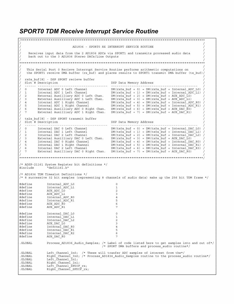
SPORT0 TDM Receive Interrupt Service Routine /**************************************************************************************************** / / / AD1836 - SPORT0 RX INTERRUPT SERVICE ROUTINE / / / / Receives input data from the 2 AD1836 ADCs via SPORT1 and transmits processed audio data / / back out to the 3 AD1836 Stereo DACs/Line Outputs / / / ***************************************************************************************************** / / / This Serial Port 0 Recieve Interrupt Service Routine performs arithmetic computations on / / the SPORT1 receive DMA buffer (rx_buf) and places results to SPORT1 transmit DMA buffer (tx_buf)/ / / / rx0a_buf[8] - DSP SPORT recieve buffer / / Slot # Description DSP Data Memory Address / / ------ -------------------------------------- ----------------------------------------------- / / 0 Internal ADC 0 Left Channel DM(rx0a_buf + 0) = DM(rx0a_buf + Internal_ADC_L0) / / 1 Internal ADC 1 Left Channel DM(rx0a_buf + 1) = DM(rx0a_buf + Internal_ADC_L1) / / 2 External Auxilliary ADC 0 Left Chan. DM(rx0a_buf + 2) = DM(rx0a_buf + AUX_ADC_L0) / / 3 External Auxilliary ADC 1 Left Chan. DM(rx0a_buf + 3) = DM(rx0a_buf + AUX_ADC_L1) / / 4 Internal ADC 1 Right Channel DM(rx0a_buf + 4) = DM(rx0a_buf + Internal_ADC_R0) / / 5 Internal ADC 1 Right Channel DM(rx0a_buf + 5) = DM(rx0a_buf + Internal_ADC_R1) / / 6 External Auxilliary ADC 0 Right Chan. DM(rx0a_buf + 6) = DM(rx0a_buf + AUX_DAC_R0) / / 7 External Auxilliary ADC 1 Right Chan. DM(rx0a_buf + 7) = DM(rx0a_buf + AUX_DAC_R1) / / / / tx2a_buf[8] - DSP SPORT transmit buffer / / Slot # Description DSP Data Memory Address / / ------ -------------------------------------- ----------------------------------------------- / / 0 Internal DAC 0 Left Channel DM(tx0a_buf + 0) = DM(tx0a_buf + Internal_DAC_L0) / / 1 Internal DAC 1 Left Channel DM(tx0a_buf + 1) = DM(tx0a_buf + Internal_DAC_L1) / / 2 Internal DAC 2 Left Channel DM(tx0a_buf + 2) = DM(tx0a_buf + Internal_DAC_L2) / / 3 External Auxilliary DAC 0 Left Chan. DM(rx0a_buf + 3) = DM(tx0a_buf + AUX_DAC_L0) / / 4 Internal DAC 0 Right Channel DM(tx0a_buf + 4) = DM(tx0a_buf + Internal_DAC_R0) / / 5 Internal DAC 1 Right Channel DM(tx0a_buf + 5) = DM(tx0a_buf + Internal_DAC_R1) / / 6 Internal DAC 2 Left Channel DM(tx0a_buf + 6) = DM(tx0a_buf + Internal_DAC_R3) / / 7 External Auxilliary DAC 0 Right Chan. DM(tx0a_buf + 7) = DM(tx0a_buf + AUX_DAC_R0) / / / ****************************************************************************************************/ /* ADSP-21161 System Register bit definitions */ #include "def21161.h" /* AD1836 TDM Timeslot Definitions */ /* 8 successive 32 bit samples (representing 8 channels of audio data) make up the 256 bit TDM frame */ #define Internal_ADC_L0 0 #define Internal_ADC_L1 1 #define AUX_ADC_L0 2 #define AUX_ADC_L1 3 #define Internal_ADC_R0 4 #define Internal_ADC_R1 5 #define AUX_ADC_R0 6 #define AUX_ADC_R1 7 #define Internal_DAC_L0 0 #define Internal_DAC_L1 1 #define Internal_DAC_L2 2 #define AUX_DAC_L0 3 #define Internal_DAC_R0 4 #define Internal_DAC_R1 5 #define Internal_DAC_R2 6 #define AUX_DAC_R0 7 .GLOBAL Process_AD1836_Audio_Samples; /* Label of code listed here to get samples into and out of*/ /* SPORT DMA buffers and process_audio routine*/ .GLOBAL Left_Channel_In0; /* These will tranfer ADC samples of interest from the*/ .GLOBAL Right_Channel_In0; /* Process_AD1836_Audio_Samples routine to the process_audio routine*/ .GLOBAL Left_Channel_In1; .GLOBAL Right_Channel_In1; .GLOBAL Left_Channel_SPDIF_rx; .GLOBAL Right_Channel_SPDIF_rx;

.GLOBAL Left_Channel_Out0; /* These will bring samples for the DACs back into the*/ .GLOBAL Right_Channel_Out0; /* Process_AD1836_Audio_Samples routine from the process_audio routine*/ .GLOBAL Left_Channel_Out1; .GLOBAL Right_Channel_Out1; .GLOBAL Left_Channel_Out2; .GLOBAL Right_Channel_Out2; .GLOBAL Left_Channel_AD1852; .GLOBAL Right_Channel_AD1852; .GLOBAL Left_Channel_Out_Thru; /* These serve the same function for a different set of audio */ .GLOBAL Right_Channel_Out_Thru;/* samples destined for the DACs*/ //.EXTERN tx2a_buf; /* These are the DMA buffers that hold the 8 channels of audio */ //.EXTERN rx0a_buf; /* immediately pre-transmission and post-reception */ //.EXTERN process_audio; /* Label of audio algorithm code listed in another file which executes */ /* a procesing alogorithm on the audio data before it is output */ /* to the DACs */ .section /dm dm_codec; /* AD1836 stereo-channel data holders - used for DSP processing of audio data received from codec */ .VAR Left_Channel_In0; /* Input values from AD1836 ADCs */ .VAR Left_Channel_In1; .VAR Right_Channel_In0; .VAR Right_Channel_In1; .VAR Left_Channel_SPDIF_rx; .VAR Right_Channel_SPDIF_rx; .VAR Left_Channel_Out0; /* Output values for AD1836 DACs */ .VAR Left_Channel_Out1; .VAR Left_Channel_Out2; .VAR Right_Channel_Out0; .VAR Right_Channel_Out1; .VAR Right_Channel_Out2; .VAR Left_Channel_AD1852; .VAR Right_Channel_AD1852; .VAR Left_Channel; /* can use for intermediate results to next filter stage */ .VAR Right_Channel; /* can use for intermediate results to next filter stage */ /* TDM audio frame/ISR counter, for debug purposes */ .VAR audio_frame_timer = 0; .section /pm pm_code; Process_AD1836_Audio_Samples: /* get AD1836 left channel input samples, save to data holders for processing */ r0 = dm(rx0a_buf + Internal_ADC_L0); dm(Left_Channel_In0) = r0; r0 = dm(rx0a_buf + Internal_ADC_L1); dm(Left_Channel_In1) = r0; r0 = dm(rx0a_buf + AUX_ADC_L0); dm(Left_Channel_SPDIF_rx) = r0; /* get AD1836 right channel input samples, save to data holders for processing */ r0 = dm(rx0a_buf + Internal_ADC_R0); dm(Right_Channel_In0) = r0; r0 = dm(rx0a_buf + Internal_ADC_R1); dm(Right_Channel_In1) = r0; r0 = dm(rx0a_buf + AUX_ADC_R0); dm(Right_Channel_SPDIF_rx) = r0; do_audio_processing: call (pc, process_audio); /* ---- DSP processing is finished, now playback results to AD1836 ---- */ playback_AD1836_left_DACs: /* output processed left ch audio samples to AD1836 */ r0 = dm(Left_Channel_Out0); dm(tx2a_buf + Internal_DAC_L0) = r0; r1 = dm(Left_Channel_Out1); dm(tx2a_buf + Internal_DAC_L1) = r1; r2 = dm(Left_Channel_Out2); dm(tx2a_buf + Internal_DAC_L2) = r2; r3 = dm(Left_Channel_AD1852); dm(tx2a_buf + AUX_DAC_L0) = r3; playback_AD1836_right_DACs: /* output processed right ch audio samples to AD1836 */ r0 = dm(Right_Channel_Out0); dm(tx2a_buf + Internal_DAC_R0) = r0; r1 = dm(Right_Channel_Out1); dm(tx2a_buf + Internal_DAC_R1) = r1; r2 = dm(Right_Channel_Out2); dm(tx2a_buf + Internal_DAC_R2) = r2; r3 = dm(Right_Channel_AD1852); dm(tx2a_buf + AUX_DAC_R0) = r3;

tx_done: r0=dm(audio_frame_timer); /* get last count */ rti(db); /* return from interrupt, delayed branch */ r0=r0+1; /* increment count */ dm(audio_frame_timer)=r0; /* save updated count */ /* ////////////////////////////////////////////////////////////////////////////////// */

APPENDIX B: C Program Source Code Listing for 21161 EZ-KIT Lite Audio Driver (Visual DSP Project Files) Main.C #include "ADDS_21161_EzKit.h" #include <def21161.h> #include <signal.h> float * DelayLine; int Index = 0; void Process_Samples( int sig_int) { Receive_Samples(); /* Perform AD1836/AD1852/SPDIF Audio Processing Here */ // left channel 1/8th inch jack to headphone out left channel Left_Channel_Out0 = Left_Channel_In1;
// left channel 1/8th inch jack to headphone out left channel Right_Channel_Out0 = Right_Channel_In1;
/* create a simple stereo digital delay on internal AD1836 stereo DAC1 channel */ Right_Channel_Out1 = DelayLine[Index] + Right_Channel_In1; // delayed left + right channel Left_Channel_Out1 = Left_Channel_In1; // loopback left channel, no processing DelayLine[Index++] = Left_Channel_In1; // store left channel into delay-line if (Index == 12000) Index = 0; /* loop back other audio data */ Left_Channel_Out2 = Left_Channel_In0; Right_Channel_Out2 = Right_Channel_In0; Left_Channel_AD1852 = Left_Channel_SPDIF_rx; Right_Channel_AD1852 = Right_Channel_SPDIF_rx; Transmit_Samples(); } void main() { /* Setup Interrupt edges and flag I/O directions */ Setup_ADSP21161N(); /* Setup SDRAM Controller */ Setup_SDRAM(); Setup_AD1836(); Init_AD1852_DACs(); Program_SPORT02_TDM_Registers(); Program_SPORT02_DMA_Channels(); interruptf( SIG_SP0I, Process_Samples); *(int *) SP02MCTL |= MCE; DelayLine = (float *) 0x00200000; for (;;) asm("idle;");

C-callable Assembly Routines for Processing Codec Data
#include <asm_sprt.h> #include <def21161.h> #include "adds_21161_ezkit.h" .segment /dm seg_dmda; /* AD1836 stereo-channel data holders - used for DSP processing of audio data received from codec */ // input channels .var _Left_Channel_In0; /* Input values from the 2 AD1836 internal stereo ADCs */ .var _Left_Channel_In1; /* 1/8th inch stereo jack connected to internal stereo ADC1 */ .var _Right_Channel_In0; .var _Right_Channel_In1; .var _Left_Channel_SPDIF_rx;/* Input values from the DAR CS8414 */ .var _Right_Channel_SPDIF_rx; //output channels .var _Left_Channel_Out0; /* Output values for the 3 AD1836 internal stereo DACs */ .var _Left_Channel_Out1; /* Left and Right Channel 0 DACs go to headphone jack */ .var _Left_Channel_Out2; .var _Right_Channel_Out0; .var _Right_Channel_Out1; .var _Right_Channel_Out2; .var _Left_Channel_AD1852; /* Output values for AD1852 stereo DAC */ .var _Right_Channel_AD1852; .var _Left_Channel; /* Can use these variables as intermediate results to next filtering stage */ .var _Right_Channel; .global _Left_Channel_In0; .global _Left_Channel_In1; .global _Right_Channel_In0; .global _Right_Channel_In1; .global _Left_Channel_Out0; .global _Left_Channel_Out1; .global _Left_Channel_Out2; .global _Right_Channel_Out0; .global _Right_Channel_Out1; .global _Right_Channel_Out2; .global _Left_Channel_AD1852; .global _Right_Channel_AD1852; .global _Left_Channel_SPDIF_rx; .global _Right_Channel_SPDIF_rx; .extern _rx0a_buf; .extern _tx2a_buf; .endseg; .segment /pm seg_pmco; _Receive_Samples: .global _Receive_Samples; //void Receive_Samples(); /* get AD1836 left channel input samples, save to data holders for processing */ r1 = -31; r0 = dm(_rx0a_buf + Internal_ADC_L0); f0 = float r0 by r1; dm(_Left_Channel_In0) = r0; r0 = dm(_rx0a_buf + Internal_ADC_L1); f0 = float r0 by r1; dm(_Left_Channel_In1) = r0; r0 = dm(_rx0a_buf + AUX_ADC_L0); f0 = float r0 by r1; dm(_Left_Channel_SPDIF_rx) = r0; /* get AD1836 right channel input samples, save to data holders for processing */ r0 = dm(_rx0a_buf + Internal_ADC_R0); f0 = float r0 by r1; dm(_Right_Channel_In0) = r0; r0 = dm(_rx0a_buf + Internal_ADC_R1); f0 = float r0 by r1; dm(_Right_Channel_In1) = r0; r0 = dm(_rx0a_buf + AUX_ADC_R0); f0 = float r0 by r1; dm(_Right_Channel_SPDIF_rx) = r0; leaf_exit; _Transmit_Samples: .global _Transmit_Samples;
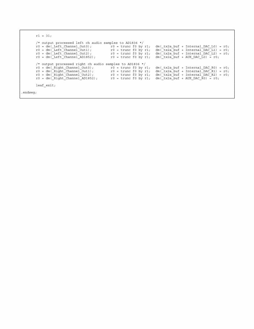
r1 = 31; /* output processed left ch audio samples to AD1836 */ r0 = dm(_Left_Channel_Out0); r0 = trunc f0 by r1; dm(_tx2a_buf + Internal_DAC_L0) = r0; r0 = dm(_Left_Channel_Out1); r0 = trunc f0 by r1; dm(_tx2a_buf + Internal_DAC_L1) = r0; r0 = dm(_Left_Channel_Out2); r0 = trunc f0 by r1; dm(_tx2a_buf + Internal_DAC_L2) = r0; r0 = dm(_Left_Channel_AD1852); r0 = trunc f0 by r1; dm(_tx2a_buf + AUX_DAC_L0) = r0; /* output processed right ch audio samples to AD1836 */ r0 = dm(_Right_Channel_Out0); r0 = trunc f0 by r1; dm(_tx2a_buf + Internal_DAC_R0) = r0; r0 = dm(_Right_Channel_Out1); r0 = trunc f0 by r1; dm(_tx2a_buf + Internal_DAC_R1) = r0; r0 = dm(_Right_Channel_Out2); r0 = trunc f0 by r1; dm(_tx2a_buf + Internal_DAC_R2) = r0; r0 = dm(_Right_Channel_AD1852); r0 = trunc f0 by r1; dm(_tx2a_buf + AUX_DAC_R0) = r0; leaf_exit; .endseg;

C code for DSP System & Codec Initialization Routines #include "ADDS_21161_EzKit.h" #include <def21161.h> #include <signal.h> /**************************************************************************************************** / / / AD1836 - SETUP and Data Routing / / / / Receives input data from the 2 AD1836 ADCs via SPORT1 and transmits processed audio data / / back out to the 3 AD1836 Stereo DACs/Line Outputs / / / ***************************************************************************************************** / / / This Serial Port 0 Recieve Interrupt Service Routine performs arithmetic computations on / / the SPORT1 receive DMA buffer (rx_buf) and places results to SPORT1 transmit DMA buffer (tx_buf)/ / / / rx0a_buf[8] - DSP SPORT recieve buffer / / Slot # Description DSP Data Memory Address / / ------ -------------------------------------- ----------------------------------------------- / / 0 Internal ADC 0 Left Channel DM(rx0a_buf + 0) = DM(rx0a_buf + Internal_ADC_L0) / / 1 Internal ADC 1 Left Channel DM(rx0a_buf + 1) = DM(rx0a_buf + Internal_ADC_L1) / / 2 External Auxilliary ADC 0 Left Chan. DM(rx0a_buf + 2) = DM(rx0a_buf + AUX_ADC_L0) / / 3 External Auxilliary ADC 1 Left Chan. DM(rx0a_buf + 3) = DM(rx0a_buf + AUX_ADC_L1) / / 4 Internal ADC 1 Right Channel DM(rx0a_buf + 4) = DM(rx0a_buf + Internal_ADC_R0) / / 5 Internal ADC 1 Right Channel DM(rx0a_buf + 5) = DM(rx0a_buf + Internal_ADC_R1) / / 6 External Auxilliary ADC 0 Right Chan. DM(rx0a_buf + 6) = DM(rx0a_buf + AUX_DAC_R0) / / 7 External Auxilliary ADC 1 Right Chan. DM(rx0a_buf + 7) = DM(rx0a_buf + AUX_DAC_R1) / / / / tx2a_buf[8] - DSP SPORT transmit buffer / / Slot # Description DSP Data Memory Address / / ------ -------------------------------------- ----------------------------------------------- / / 0 Internal DAC 0 Left Channel DM(tx0a_buf + 0) = DM(tx0a_buf + Internal_DAC_L0) / / 1 Internal DAC 1 Left Channel DM(tx0a_buf + 1) = DM(tx0a_buf + Internal_DAC_L1) / / 2 Internal DAC 2 Left Channel DM(tx0a_buf + 2) = DM(tx0a_buf + Internal_DAC_L2) / / 3 External Auxilliary DAC 0 Left Chan. DM(rx0a_buf + 3) = DM(tx0a_buf + AUX_DAC_L0) / / 4 Internal DAC 0 Right Channel DM(tx0a_buf + 4) = DM(tx0a_buf + Internal_DAC_R0) / / 5 Internal DAC 1 Right Channel DM(tx0a_buf + 5) = DM(tx0a_buf + Internal_DAC_R1) / / 6 Internal DAC 2 Left Channel DM(tx0a_buf + 6) = DM(tx0a_buf + Internal_DAC_R3) / / 7 External Auxilliary DAC 0 Right Chan. DM(tx0a_buf + 7) = DM(tx0a_buf + AUX_DAC_R0) / / / ****************************************************************************************************/ int powerdown_AD1836[4] = {DAC_CONTROL1 | WRITE_REG | 0x004, DAC_CONTROL1 | WRITE_REG | 0x004, ADC_CONTROL1 | WRITE_REG | 0x080, ADC_CONTROL1 | WRITE_REG | 0x080}; int powerdown_rx_buf0a[4]; // rx dma dummy buffer not used for anything; // AD1836 codec register commands - Serial SPI 16-bit Word Format as follows: // D15 to D12 = Codec Register Address // D11 = Read/Write register (1=rd, 0=wr // D10 = reserved bit, clear to zero // D9 to D0 = Data Field for codec register #define TX_BUF3A_LEN 21 int tx_buf3a[TX_BUF3A_LEN] = //program register commands
{DAC_CONTROL1 | WRITE_REG | 0x000, // we "OR" in address, rd/wr, and register data DAC_CONTROL1 | WRITE_REG | 0x000, // for ease in reading register values DAC_CONTROL2 | WRITE_REG | 0x000, // write DAC_CTL1 twice to workaround pwdwn SPI anomaly
DAC_VOLUME0 | WRITE_REG | 0x3FF, DAC_VOLUME1 | WRITE_REG | 0x3FF, DAC_VOLUME2 | WRITE_REG | 0x3FF, DAC_VOLUME3 | WRITE_REG | 0x3FF, DAC_VOLUME4 | WRITE_REG | 0x3FF, DAC_VOLUME5 | WRITE_REG | 0x3FF, ADC_CONTROL1 | WRITE_REG | 0x000, // write ADC_CTL1 twice to workaround pwdwn SPI anomaly ADC_CONTROL1 | WRITE_REG | 0x000, ADC_CONTROL3 | WRITE_REG | 0x000, // 256*Fs Clock Mode !!!, differential PGA mode ADC_CONTROL2 | WRITE_REG | 0x380, // SOUT MODE = 110 --> TDM Mode, Master device

ADC_CONTROL2 | WRITE_REG | 0x380, // read register commands ADC0_PEAK_LEVEL | READ_REG | 0x000, // status will be in rx_buf1a[13-19] memory locations ADC1_PEAK_LEVEL | READ_REG | 0x000, ADC2_PEAK_LEVEL | READ_REG | 0x000, ADC3_PEAK_LEVEL | READ_REG | 0x000, ADC_CONTROL1 | READ_REG | 0x000, ADC_CONTROL2 | READ_REG | 0x000, ADC_CONTROL3 | READ_REG | 0x000 }; #define RX_BUF1A_LEN 21 int rx_buf1a[RX_BUF1A_LEN]; void SPORT_RX_IRQ( int sig_int) {} int Setup_AD1836() { int i; /* Powerdown reset of AD1836 */ *(int *) II3A = (int) powerdown_AD1836; *(int *) IM3A = 1; *(int *) C3A = 4; *(int *) II1A = (int) powerdown_rx_buf0a; *(int *) IM1A = 1; *(int *) C1A = 4; *(int *) SP13MCTL = 0; *(int *) DIV3 = 0x0011002B; *(int *) DIV1 = 0; *(int *) SPCTL3 |= DDIR | SDEN_A | LAFS | LFS | IFS | FSR | CKRE | ICLK | SLEN16 | SPEN_A; *(int *) SPCTL1 |= SDEN_A | LAFS | LFS | FSR | CKRE | SLEN16 | SPEN_A; *(int *) SPCTL1 &= (~DDIR & ~IFS & ~ICLK); interruptf( SIG_SP1I, SPORT_RX_IRQ); interruptf( SIG_SP3I, SPORT_RX_IRQ); while ( (*(int*) DMASTAT) & 0x8 ) asm("idle;"); interruptf( SIG_SP1I, SIG_IGN); interruptf( SIG_SP3I, SIG_IGN); /* Now, stall for about 1 second */ for (i=0;i<3000;i++) asm("nop; nop; nop; nop; nop;"); *(int *) SPCTL1 = 0; *(int *) SPCTL3 = 0; /* SPORT DMA Setup */ *(int *) II3A = (int) tx_buf3a; *(int *) IM3A = 1; *(int *) C3A = TX_BUF3A_LEN; *(int *) II1A = (int) rx_buf1a; *(int *) IM1A = 1; *(int *) C1A = RX_BUF1A_LEN; *(int *) SP13MCTL = 0; *(int *) DIV3 = 0x0011002B; *(int *) DIV1 = 0; *(int *) SPCTL3 |= DDIR | SDEN_A | LAFS | LFS | IFS | FSR | CKRE | ICLK | SLEN16 | SPEN_A; *(int *) SPCTL1 |= SDEN_A | LAFS | LFS | FSR | CKRE | SLEN16 | SPEN_A; *(int *) SPCTL1 &= (~DDIR & ~IFS & ~ICLK); interruptf( SIG_SP1I, SPORT_RX_IRQ); interruptf( SIG_SP3I, SPORT_RX_IRQ);

while ( (*(int*) DMASTAT) & 0xA ) asm("idle;"); interruptf( SIG_SP1I, SIG_IGN); interruptf( SIG_SP3I, SIG_IGN); *(int *) SPCTL1 = 0; *(int *) SPCTL3 = 0; return 0; } int rx0a_buf[8]; /* receive buffer (DMA)*/ int tx2a_buf[8] = { 0x00000000, /* transmit buffer (DMA)*/ 0x00000000, 0x00000000, 0x00000000, 0x00000000, 0x00000000, 0x00000000, 0x00000000}; /* TCB = "Transfer Control Block" */ /* TCB format: ECx (length of destination buffer), EMx (destination buffer step size), EIx (destination buffer index (initialized to start address)), GPx ("general purpose"), CPx ("Chain Point register"; points to last address (IIx) of next TCB to jump to upon completion of this TCB.), Cx (length of source buffer), IMx (source buffer step size), IIx (source buffer index (initialized to start address)) */ int rcv0a_tcb[8] = {0, 0, 0, 0, 0, 8, 1, (int) rx0a_buf}; /* SPORT0 receive tcb */ int xmit2a_tcb[8] = {0, 0, 0, 0, 0, 8, 1, (int) tx2a_buf}; /* SPORT2 transmit tcb */ void Program_SPORT02_TDM_Registers() { *(int *) DIV0 = 0; *(int *) DIV2 = 0; /* SPORT0 and SPORT2 are being operated in "multichannel" mode. This is synonymous with TDM mode which is the operating mode for the AD1836 */ /* SPORT 0&2 Miscellaneous Control Bits Registers */ /* SP02MCTL = 0x000000E2, Hold off on MCM enable, and number of TDM slots to 8 active channels */ /* Multichannel Frame Delay=1, Number of Channels = 8, LB disabled */ *(int *) SP02MCTL = NCH_8 | MFD1; /* sport0 control register set up as a receiver in MCM */ /* sport 0 control register SPCTL0 = 0x000C01F0 */ *(int *) SPCTL0 = SCHEN_A | SDEN_A | SLEN32; /* sport2 control register set up as a transmitter in MCM */ /* sport 2 control register, SPCTL2 = 0x000C01F0 */ *(int *) SPCTL2 = SCHEN_A | SDEN_A | SLEN32; /* sport0 & sport2 receive and transmit multichannel word enable registers */ /* enable receive channels 0-7 */ /* enable transmit channels 0-7 */ *(int *) MR0CS0 = *(int *) MT2CS0 =0x000000FF; /* sport0 & sport2 receive & transmit multichannel companding enable registers */ /* no companding for our 8 active timeslots*/ /* no companding on SPORT0 receive */ /* no companding on SPORT2 transmit */ *(int *) MR0CCS0 = *(int *) MT2CCS0 = 0; }

void Program_SPORT02_DMA_Channels() { xmit2a_tcb[4] = *(int *) CP2A = ((int) xmit2a_tcb + 7) & 0x3FFFF | (1<<18); rcv0a_tcb[4] = *(int *) CP0A = ((int) rcv0a_tcb + 7) & 0x3FFFF | (1<<18); } #ifdef DEBUG /* TDM audio frame/ISR counter, for debug purposes */ int audio_frame_timer = 0; #endif /* AD1852 Setup */ #define SPI_TX_BUF_LEN 5 int spi_tx_buf[SPI_TX_BUF_LEN] = { RESET_AD1852 | CONTROL_REG, // reset AD1852 DEASSERT_RESET | CONTROL_REG, // remove reset command WL_24_BIT_DATA | I2S_JUSTIFIED | NO_DEMPH_FILTER | CONTROL_REG, 0x00FC | VOLUME_LEFT, 0x00FC | VOLUME_RIGHT }; void Init_AD1852_DACs() { // initially clear SPI control register *(int *) SPICTL = 0; *(int *) IISTX = (int) spi_tx_buf; *(int *) IMSTX = 1; *(int *) CSTX = SPI_TX_BUF_LEN; asm("#include <def21161_may2001.h>"); asm("bit set LIRPTL SPITMSK;"); interruptf( SIG_LP0I, SPORT_RX_IRQ); *(int *) SPICTL |= SPIEN|SPTINT|TDMAEN|MS|FLS1|CPHASE|DF|WL16|BAUDR4|PSSE|DCPH0|SGN|GM;
*(int *) SPICTL &= (~CP & ~FLS0 & ~FLS2 & ~FLS3 & ~SMLS & ~DMISO & ~OPD & ~PACKEN & ~SENDZ & ~RDMAEN & ~SPRINT); while( (*(int*) DMASTAT) & DMA9ST) idle(); interruptf( SIG_LP0I, SIG_IGN); asm("bit clr LIRPTL SPITMSK;"); *(int *) SPICTL = 0; } /* SDRAM Setup Routine */ void Setup_SDRAM() { /*clear MSx waitstate and mode*/ *(int *)WAIT &= 0xFFF00000; /*refresh rate*/ *(int*) SDRDIV = 0x1000; // SDCTL = 0x02014231; // 1/2 CCLK, no SDRAM buffering option, 2 SDRAM banks // SDRAM mapped to bank 0 only, no self-refresh, page size 256 words // SDRAM powerup mode is prechrg, 8 CRB refs, and then mode reg set cmd // tRCD = 2 cycles, tRP=2 cycles, tRAS=3 cycles, SDCL=1 cycle // SDCLK0, SDCLK1, RAS, CAS and SDCLKE activated *(int *) SDCTL |= SDTRCD2|SDCKR_DIV2|SDBN2|SDEM0|SDPSS|SDPGS256|SDTRP2|SDTRAS3|SDCL1; *(int *) SDCTL &= ~SDBUF & ~SDEM3 & ~SDEM2 & ~SDEM1 & ~SDSRF & ~SDPM & ~DSDCK1 & ~DSDCTL; } /* DSP Setup */ void Setup_ADSP21161N() { /* *** Enable circular buffering in MODE1 Register for revision 0.x silicon. Important when porting 2106x code!!! */ asm("bit set MODE1 CBUFEN;"); /* Setup hardware interrupts, FLAG LEDs and pushbutton */

*(int *) IOFLAG = FLG9|FLG8|FLG7|FLG6|FLG5|FLG4|FLG9O|FLG8O|FLG7O|FLG6O|FLG5O|FLG4O; /* flag 0-3 are inputs from pushbutton switches */ asm("bit clr MODE2 FLG0O | FLG1O | FLG2O | FLG3O;"); /* irqx edge sensitive */ asm("bit set mode2 IRQ2E | IRQ0E | IRQ1E;"); } void Blink_LED_Test( int interations ) { int i,k; for(i=0;i<interations;i++) { *(int*) IOFLAG ^= FLG9|FLG8|FLG7|FLG6|FLG5|FLG4; for (k=0;k<10000000;k++) {} } }

C code for DSP System & Codec Initialization Routines #ifdef __ECC__ /* Insert C Definitions here.... */ int Setup_AD1836(); void Program_SPORT02_TDM_Registers(); void Program_SPORT02_DMA_Channels(); void Receive_Samples(); void Transmit_Samples(); void Init_AD1852_DACs(); void Setup_SDRAM(); void Setup_ADSP21161N(); void Blink_LED_Test( int interations ); extern float Left_Channel0; /* Input values from AD1836 ADCs */ extern float Left_Channel1; extern float Left_Channel2; extern float Left_Channel3; /* AD1852 */ extern float Right_Channel0; extern float Right_Channel1; extern float Right_Channel2; extern float Right_Channel3; /* AD1852 */ extern float Left_Channel_SPDIF_rx; extern float Right_Channel_SPDIF_rx; // input channels extern float Left_Channel_In0; /* Input values from the 2 AD1836 internal stereo ADCs */ extern float Left_Channel_In1; /* 1/8th inch stereo jack connected to internal stereo ADC1 */ extern float Right_Channel_In0; extern float Right_Channel_In1; extern float Left_Channel_SPDIF_rx; /* Input values from the DAR CS8414 */ extern float Right_Channel_SPDIF_rx; //output channels extern float Left_Channel_Out0; /* Output values for the 3 AD1836 internal stereo DACs */ extern float Left_Channel_Out1; /* Left and Right Channel 0 DACs go to headphone jack */ extern float Left_Channel_Out2; extern float Right_Channel_Out0; extern float Right_Channel_Out1; extern float Right_Channel_Out2; extern float Left_Channel_AD1852; /* Output values for AD1852 stereo DAC */ extern float Right_Channel_AD1852; #else /* Insert Assembly Definitions here.... */ #endif /* Insert global definitions here */ // AD1836 codec SPI control/status register definitions #define READ_REG 0x0800 #define WRITE_REG 0x0000 #define DAC_CONTROL1 0x0000 #define DAC_CONTROL2 0x1000 #define DAC_VOLUME0 0x2000 #define DAC_VOLUME1 0x3000 #define DAC_VOLUME2 0x4000 #define DAC_VOLUME3 0x5000 #define DAC_VOLUME4 0x6000 #define DAC_VOLUME5 0x7000 #define ADC0_PEAK_LEVEL 0x8000 #define ADC1_PEAK_LEVEL 0x9000 #define ADC2_PEAK_LEVEL 0xA000 #define ADC3_PEAK_LEVEL 0xB000 #define ADC_CONTROL1 0xC000 #define ADC_CONTROL2 0xD000 #define ADC_CONTROL3 0xE000 #define RESERVED_REG 0xF000 #define NCH_8 0x000000E0 /* Number of MCM channels - 1 */ #define Initialize_TDM 0xD380 /* 1101 0001 1000 0000*/

/* AD1836 TDM Timeslot Definitions */ #define Internal_ADC_L0 0 #define Internal_ADC_L1 1 #define AUX_ADC_L0 2 #define AUX_ADC_L1 3 #define Internal_ADC_R0 4 #define Internal_ADC_R1 5 #define AUX_ADC_R0 6 #define AUX_ADC_R1 7 #define Internal_DAC_L0 0 #define Internal_DAC_L1 1 #define Internal_DAC_L2 2 #define AUX_DAC_L0 3 #define Internal_DAC_R0 4 #define Internal_DAC_R1 5 #define Internal_DAC_R2 6 #define AUX_DAC_R0 7 /* Leave a safety margin of 5x for the 1836 */ #define AD1836_RESET_CYCLES 300 #define AD1836_WARMUP_CYCLES 60000 /* AD1852 Defines */ #define VOLUME_LEFT 0x0 #define VOLUME_RIGHT 0x2 #define CONTROL_REG 0x1 // AD1852 control word parameters #define DEASSERT_RESET 0x0000 #define INTERP2xMODE 0x0800 #define INTERP4xMODE 0x0400 #define WL_24_BIT_DATA 0x0000 #define WL_20_BIT_DATA 0x0100 #define WL_16_BIT_DATA 0x0200 #define RESET_AD1852 0x0080 #define SOFT_MUTE 0x0040 #define RIGHT_JUSTIFIED 0x0000 #define I2S_JUSTIFIED 0x0010 #define LEFT_JUSTIFIED 0x0020 #define DSP_SERIAL 0x0030 #define NO_DEMPH_FILTER 0x0000 #define FILTER_44_1_kHz 0x0004 #define FILTER_32_kHz 0x0008 #define FILTER_48_kHz 0x000C /* SDRAM Defines */ #define sdram_size 0xfffff

ADSP-21161 Interrupt Vector Table /* ************************************************************************************ */ /* */ /* ADSP-21161 INTERRUPT VECTOR TABLE */ /* */ /* For use with the 21161 EZ-KIT Lite */ /* */ /* ADI DSP Central Applications Engineering */ /* 10/3/00 */ /* ************************************************************************************ */ .EXTERN _main; .EXTERN Init_DSP; .EXTERN Count_SPORT1_RX_IRQs; .EXTERN Count_SPORT3_TX_IRQs; .EXTERN Process_AD1836_Audio_Samples; .section /dm dm_data; /* SPORT TX ISR counter, for debug purposes */ .VAR SPORT2_TXDMA_counter = 0; .section/PM isr_tbl; /* 21161 Interrupt Service Table */ /* 0x00 Reserved Interrupt */ /* 0x00 0x01 0x02 0x03 */ /* NOP; NOP; NOP; NOP; */ // Reserved interrupt // Vector for RESET: /* 0x04 - reset vector starts at location 0x40005 */ RSTI_scv: /* IDLE; */ // Implicit IDLE instruction for boot kernel cleanup call Init_DSP; NOP; jump _main; /* 0x08 - Vector address for illegal input condition detected */ IICD_svc: RTI; RTI; RTI; RTI; /* 0x0C - Vector address for status stack/loop stack overflow or PC stack full: */ SOVFI_svc: RTI; RTI; RTI; RTI; // 0x10 - Vector address for high priority timer interrupt: TMZHI_svc: RTI; RTI; RTI; RTI; // 0x14 - Vector address for Vector Interrupt: VIRPTI_svc: RTI; RTI; RTI; RTI; // 0x18 - Vector address for Hardware Interrupt 2 (IRQ2): IRQ2I_svc: RTI; RTI; RTI; RTI;; // 0x1C - Vector address for Hardware Interrupt 1 (IRQ1): IRQ1I_svc: RTI; RTI; RTI; RTI; // 0x20 - Vector address for Hardware Interrupt 0 (IRQ0): IRQ0I_svc: RTI; RTI; RTI; RTI; /* 0x24 - Reserved interrupt */ reserved_0x24: NOP; NOP; NOP; NOP; // Reserved interrupt // Vectors for Serial port DMA channels: /* 0x28 - Vector address for serial port 0 primary A, secondary B RX/TX buffers (DMA Channels 0 & 1) */ SP0I_svc: JUMP Process_AD1836_Audio_Samples; RTI; RTI; RTI; /* 0x2C - Vector address for serial port 1 primary A, secondary B RX/TX buffers (DMA Channel 2 & 3) */ SP1I_svc: JUMP Count_SPORT1_RX_IRQs; RTI; RTI; RTI; /* 0x30 - Vector address for serial port 2 primary A, secondary B RX/TX buffers (DMA Channel 4 & 5) */ SP2I_svc: r0=dm(SPORT2_TXDMA_counter); /* get last count */ RTI(db); r0=r0+1; /* increment count */ dm(SPORT2_TXDMA_counter)=r0; /* save updated count */

/* 0x34 - Vector address for serial port 3 primary A, secondary B RX/TX buffers (DMA Channel 6 & 7) */ SP3I_svc: JUMP Count_SPORT3_TX_IRQs; RTI; RTI; RTI; // Vectors for link port DMA channels: /* 0x38 - Vector address for Link Buffer 0 (DMA Channel 8) */ LP0I_svc: RTI; RTI; RTI; RTI; /* 0x3C - Vector address for Link Buffer 1 (DMA Channel 9) */ LP1I_svc: RTI; RTI; RTI; RTI; /* 0x40 - Vector address for SPI Receive (DMA Channel 8) */ SPIRI_svc: RTI; RTI; RTI; RTI; /* 0x44 - Vector address for SPI Receive (DMA Channel 9) */ SPITI_svc: RTI; RTI; RTI; RTI; /* 0x48 - Reserved Interrupt */ reserved_0x48: RTI; RTI; RTI; RTI; /* 0x4C - Reserved Interrupt */ reserved_0x4C: RTI; RTI; RTI; RTI; // Vectors for External port DMA channels: /* 0x50 - Vector address for External Port Buffer 0 (DMA Channel 10) */ EP0I_svc: RTI; RTI; RTI; RTI; /* 0x54 - Vector address for External Port Buffer 0 (DMA Channel 11) */ EP1I_svc: RTI; RTI; RTI; RTI; /* 0x58 - Vector address for External Port Buffer 0 (DMA Channel 12) */ EP2I_svc: RTI; RTI; RTI; RTI; /* 0x5C - Vector address for External Port Buffer 0 (DMA Channel 13) */ EP3I_svc: RTI; RTI; RTI; RTI; // 0x60 - Vector address for Link service request: LSRQI_svc: RTI; RTI; RTI; RTI; // 0x64 - Vector address for DAG1 buffer 7 circular buffer overflow: CB7I_svc: RTI; RTI; RTI; RTI; // 0x68 - Vector address for DAG2 buffer 15 circular buffer overflow: CB15I_svc: RTI; RTI; RTI; RTI; // 0x6C - Vector address for lower priority timer interrupt: TMZLI_svc: RTI; RTI; RTI; RTI; // 0x70 - Vector address for fixed-point overflow interrupt: FIXI_svc: RTI; RTI; RTI; RTI; // 0x74 - Vector address for floating-point overflow exception interrupt: FLTOI_svc: RTI; RTI; RTI; RTI; // 0x78 - Vector address for floating-point underflow exception interrupt: FLTUI_svc: RTI; RTI; RTI; RTI; // 0x7C - Vector address for floating-point invalid exception interrupt: FLTII_svc: RTI; RTI; RTI; RTI; // 0x80 - Vector address for user software interrupt 0: SFT0I_svc: RTI; RTI; RTI; RTI; // 0x84 - Vector address for user software interrupt 1: SFT1I_svc: RTI; RTI; RTI; RTI; // 0x88 - Vector address for user software interrupt 2: SFT2I_svc: RTI; RTI; RTI; RTI; // 0x8C - Vector address for user software interrupt 3: SFT3I_svc: RTI; RTI; RTI; RTI; /* 0x90 - Reserved Interrupt */ reserved_0x90: RTI; RTI; RTI; RTI;

Visual DSP Tools (21161 EZ-KIT Lite) Linker Description File ARCHITECTURE(ADSP-21161) // // ADSP-21161 Memory Map: // ------------------------------------------------ // Internal memory 0x0000 0000 to 0x000f ffff // ------------------------------------------------ // 0x0000 0000 to 0x0001 ffff IOP Regs // Block 0 0x0002 0000 to 0x0002 1fff Long Word (64) Addresses // 0x0002 2000 to 0x0002 7fff (reserved) // Block 1 0x0002 8000 to 0x0002 9fff Long Word (64) Addresses // 0x0002 a000 to 0x0003 ffff (reserved) // Block 0 0x0004 0000 to 0x0004 3fff Normal Word (32/48) Addresses // 0x0004 4000 to 0x0004 ffff (reserved) // Block 1 0x0005 0000 to 0x0005 3fff Normal Word (32/48) Addresses // 0x0005 4000 to 0x0007 ffff (reserved) // Block 0 0x0008 0000 to 0x0008 7fff Short Word (16) Addresses // 0x0008 8000 to 0x0009 ffff (reserved) // Block 1 0x000a 0000 to 0x000a 7fff Short Word (16) Addresses // 0x000a 8000 to 0x000f ffff (reserved) // ------------------------------------------------ // Multiproc memory 0x0010 0000 to 0x007f ffff // ------------------------------------------------ // 0x0010 0000 to 0x0011 ffff Hammerhead ID=001 Internal memory // 0x0012 0000 to 0x0013 ffff Hammerhead ID=010 Internal memory // 0x0014 0000 to 0x0015 ffff Hammerhead ID=011 Internal memory // 0x0016 0000 to 0x0017 ffff Hammerhead ID=100 Internal memory // 0x0018 0000 to 0x0019 ffff Hammerhead ID=101 Internal memory // 0x001a 0000 to 0x001b ffff Hammerhead ID=110 Internal memory // 0x001c 0000 to 0x001f ffff Hammerhead ID=all Internal memory // ------------------------------------------------ // External memory 0x0020 0000 to 0xffff ffff // ------------------------------------------------ // // This architecture file allocates: // Internal 256 words of run-time header in memory block 0 // 256 words of initialization code in memory block 0 // 6K words of C code space in memory block 0 // 1.5K words of C PM data space in memory block 0 // 8K words of C DM data space in memory block 1 // 4K words of C heap space in memory block 1 // 4K words of C stack space in memory block 1 SEARCH_DIR( $ADI_DSP\211xx\lib ) $LIBRARIES = libc160.dlb, libio160_32.dlb, libdsp160.dlb, libcpp.dlb, libcpprt.dlb; // Libraries from the command line are included in COMMAND_LINE_OBJECTS. #ifdef __cplusplus $OBJECTS = 160_cpp_hdr.doj, $COMMAND_LINE_OBJECTS; #else //$OBJECTS = 160_hdr.doj, $COMMAND_LINE_OBJECTS; $OBJECTS = $COMMAND_LINE_OBJECTS; #endif MEMORY { seg_rth { TYPE(PM RAM) START(0x00040005) END(0x000400ff) WIDTH(48) } seg_init { TYPE(PM RAM) START(0x00040100) END(0x000401ff) WIDTH(48) } seg_pmco { TYPE(PM RAM) START(0x00040200) END(0x000419ff) WIDTH(48) } seg_pmda { TYPE(PM RAM) START(0x00042a00) END(0x00043fff) WIDTH(32) } #ifdef __cplusplus seg_ctdm { TYPE(DM RAM) START(0x00050000) END(0x000500ff) WIDTH(32) } seg_ctdmend { TYPE(DM RAM) START(0x00050100) END(0x000501ff) WIDTH(32) } seg_dmda { TYPE(DM RAM) START(0x00050200) END(0x00051fff) WIDTH(32) } #else seg_dm48 { TYPE(PM RAM) START(0x00050000) END(0x000500ff) WIDTH(48) } seg_dm32 { TYPE(DM RAM) START(0x00050200) END(0x000502ff) WIDTH(32) } seg_dmda { TYPE(DM RAM) START(0x00050300) END(0x00051fff) WIDTH(32) } #endif seg_heap { TYPE(DM RAM) START(0x00052000) END(0x00052fff) WIDTH(32) }
seg_stak { TYPE(DM RAM) START(0x00053000) END(0x00053fff) WIDTH(32) } // External Memory SDRAM Mapped to Bank 0 segsdram { TYPE(DM RAM) START(0x00200000) END(0x002FFFFF) WIDTH(32) } } PROCESSOR p0 { LINK_AGAINST( $COMMAND_LINE_LINK_AGAINST) OUTPUT( $COMMAND_LINE_OUTPUT_FILE ) SECTIONS { // .text output section seg_rth { INPUT_SECTIONS( $OBJECTS(isr_tbl) $LIBRARIES(isr_tbl)) } >seg_rth seg_init { ldf_seginit_space = . ; INPUT_SECTIONS( $OBJECTS(seg_init) $LIBRARIES(seg_init)) } >seg_init seg_pmco { INPUT_SECTIONS( $OBJECTS(pm_code) $LIBRARIES(pm_code)) } >seg_pmco seg_pmda { INPUT_SECTIONS( $OBJECTS(pm_data) $LIBRARIES(pm_data)) } >seg_pmda #ifdef __cplusplus seg_ctdm { __ctors = .; /* points to the start of the section */ INPUT_SECTIONS( $OBJECTS(seg_ctdm) $LIBRARIES(seg_ctdm)) } > seg_ctdm seg_ctdmend { INPUT_SECTIONS( $OBJECTS(seg_ctdmend) $LIBRARIES(seg_ctdmend)) } > seg_ctdmend #endif seg_dm48 { INPUT_SECTIONS( $OBJECTS(seg_dm48) $LIBRARIES(seg_dm48)) } > seg_dm48 seg_dm32 { INPUT_SECTIONS( $OBJECTS(seg_dm32) $LIBRARIES(seg_dm32)) } > seg_dm32 seg_dmda { INPUT_SECTIONS( $OBJECTS(dm_data dm_codec) $LIBRARIES(dm_data)) } > seg_dmda stackseg { // allocate a stack for the application ldf_stack_space = .; ldf_stack_length = MEMORY_SIZEOF(seg_stak); } > seg_stak heap { // allocate a heap for the application

ldf_heap_space = .; ldf_heap_end = ldf_heap_space + MEMORY_SIZEOF(seg_heap) - 1; ldf_heap_length = ldf_heap_end - ldf_heap_space; } > seg_heap segsdram SHT_NOBITS { INPUT_SECTIONS( $OBJECTS(segsdram) $LIBRARIES(segsdram)) } > segsdram } }
Disclaimer Information furnished by Analog Devices, Inc., is believed to be accurate and reliable. However, no responsibility is assumed by Analog Devices Inc., for its use; nor for any infringements of patents or other rights of third parties which may result from its use. No license is granted by implication or otherwise under the patent rights of Analog Devices. Analog Devices Inc. reserves the right to make changes without further notice to any products here-in. Analog Devices makes no warranty, representation or guarantee regarding the suitability of its DSP and codec products for any particular purpose, nor does Analog Devices assume any liability arising out of the application or use of our DSP and codec products, and specifically disclaims any and all liability, including without limitation consequential or incidental damages. Operating parameters such as temperature and voltage can and do vary in different applications. All operating parameters as specified in Analog Devices data sheets must be validated for each customer application by customer’s technical experts. Analog Device's DSP and codec products are not designed, intended, or authorized for use as components in which the failure of the ADI product could create a situation where personal injury or death may occur. If the Buyer/User uses ADI products for any unintended or unauthorized application, then ADI cannot be held responsible.