pcb & layout
TRANSCRIPT
1
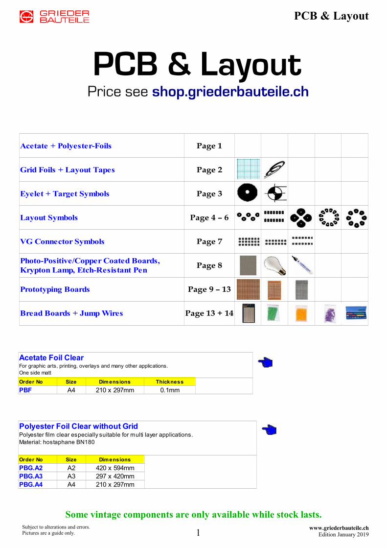
PCB & Layout
www.griederbauteile.chEdition January 2019
Subject to alterations and errors.Pictures are a guide only.
PCB & Layout
Price see shop.griederbauteile.ch
Acetate + Polyester-Foils Page 1
Grid Foils + Layout Tapes Page 2
Eyelet + Target Symbols Page 3
Layout Symbols Page 4 – 6 s
VG Connector Symbols Page 7
Page 8
Prototyping Boards Page 9 – 13
Bread Boards + Jump Wires Page 13 + 14
Photo-Positive/Copper Coated Boards, Krypton Lamp, Etch-Resistant Pen
Order No Size Dimensions Thickness
PBF A4 210 x 297mm 0.1mm
Acetate Foil ClearFor graphic arts, printing, overlays and many other applications.One side matt
Order No Size Dimensions
PBG.A2 A2 420 x 594mmPBG.A3 A3 297 x 420mmPBG.A4 A4 210 x 297mm
Polyester Foil Clear without GridPolyester film clear especially suitable for multi layer applications.Material: hostaphane BN180
Some vintage components are only available while stock lasts.
2
PCB & Layout
www.griederbauteile.chEdition January 2019
Subject to alterations and errors.Pictures are a guide only.
Order No Size Grid section Grid
PBP.250.A3 A3 277 x 400mm 2.50mm/.098”PBP.250.A4 A4 190 x 277mm 2.50mm/.098”PBP.254.A3 A3 277 x 400mm 2.54mm/.100”PBP.254.A4 A4 190 x 277mm 2.54mm/.100”
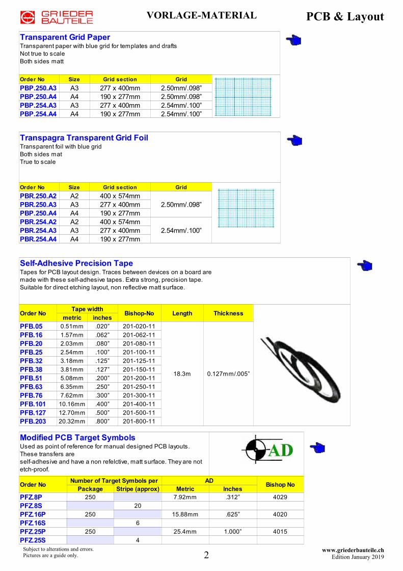
Transparent Grid PaperTransparent paper with blue grid for templates and draftsNot true to scaleBoth sides matt
Order No Size Grid section Grid
PBR.250.A2 A2 400 x 574mm2.50mm/.098”PBR.250.A3 A3 277 x 400mm
PBP.250.A4 A4 190 x 277mmPBR.254.A2 A2 400 x 574mm
2.54mm/.100”PBR.254.A3 A3 277 x 400mmPBR.254.A4 A4 190 x 277mm
Transpagra Transparent Grid FoilTransparent foil with blue gridBoth sides matTrue to scale
VORLAGE-MATERIAL
Order NoTape width
Bishop-No Length Thicknessmetric inches
PFB.05 0.51mm .020” 201-020-11
18.3m 0.127mm/.005”
PFB.16 1.57mm .062” 201-062-11
PFB.20 2.03mm .080” 201-080-11
PFB.25 2.54mm .100” 201-100-11
PFB.32 3.18mm .125” 201-125-11
PFB.38 3.81mm .127” 201-150-11
PFB.51 5.08mm .200” 201-200-11
PFB.63 6.35mm .250” 201-250-11
PFB.76 7.62mm .300” 201-300-11
PFB.101 10.16mm .400” 201-400-11
PFB.127 12.70mm .500” 201-500-11
PFB.203 20.32mm .800” 201-800-11
Self-Adhesive Precision TapeTapes for PCB layout design. Traces between devices on a board are made with these self-adhesive tapes. Extra strong, precision tape.Suitable for direct etching layout, non reflective matt surface.
Order NoNumber of Target Symbols per AD
Bishop NoPackage Stripe (approx) Metric Inches
PFZ.8P 250 7.92mm .312” 4029
PFZ.8S 20
PFZ.16P 250 15.88mm .625” 4020
PFZ.16S 6
PFZ.25P 250 25.4mm 1.000” 4015
PFZ.25S 4
Modified PCB Target SymbolsUsed as point of reference for manual designed PCB layouts. These transfers are self-adhesive and have a non refelctive, matt surface. They are not etch-proof.
3
PCB & Layout
www.griederbauteile.chEdition January 2019
Subject to alterations and errors.Pictures are a guide only.
Order NoNumber of Eyelets per AD ID
Bishop NoPackage Stripe (approx) Metric Inches Metric Inches
PFE.16P 5001.57mm .062” 0.63mm .025” D136
PFE.16S 36
PFE.20P 5002.03mm .080” 0.79mm .031” D216
PFE.20S 29
PFE.51P 5005.08mm .200” 1.02mm .040” D204
PFE.51S 52
PFE.63P 5006.35mm .250” 1.02mm .040” D108
PFE.63S 24
PFE.76P 5007.62mm .300” 1.02mm .040” D293
PFE.76S 20
PFE.101P 50010.16mm .400” 1.02mm .040” D189
PFE.101S 16
PFE.127P 50012.70mm .500” 1.02mm .040” D192
PFE.127S 24
PFE.152P 50015.24mm .600” 1.57mm .062” D149
PFE.152S 22
PFE.203P 50020.32mm .800” 1.57mm .062” D235
PFE.203S 9
PFE.254P 50025.40mm 1.000” 1.57mm .062” D131
PFE.254S 7
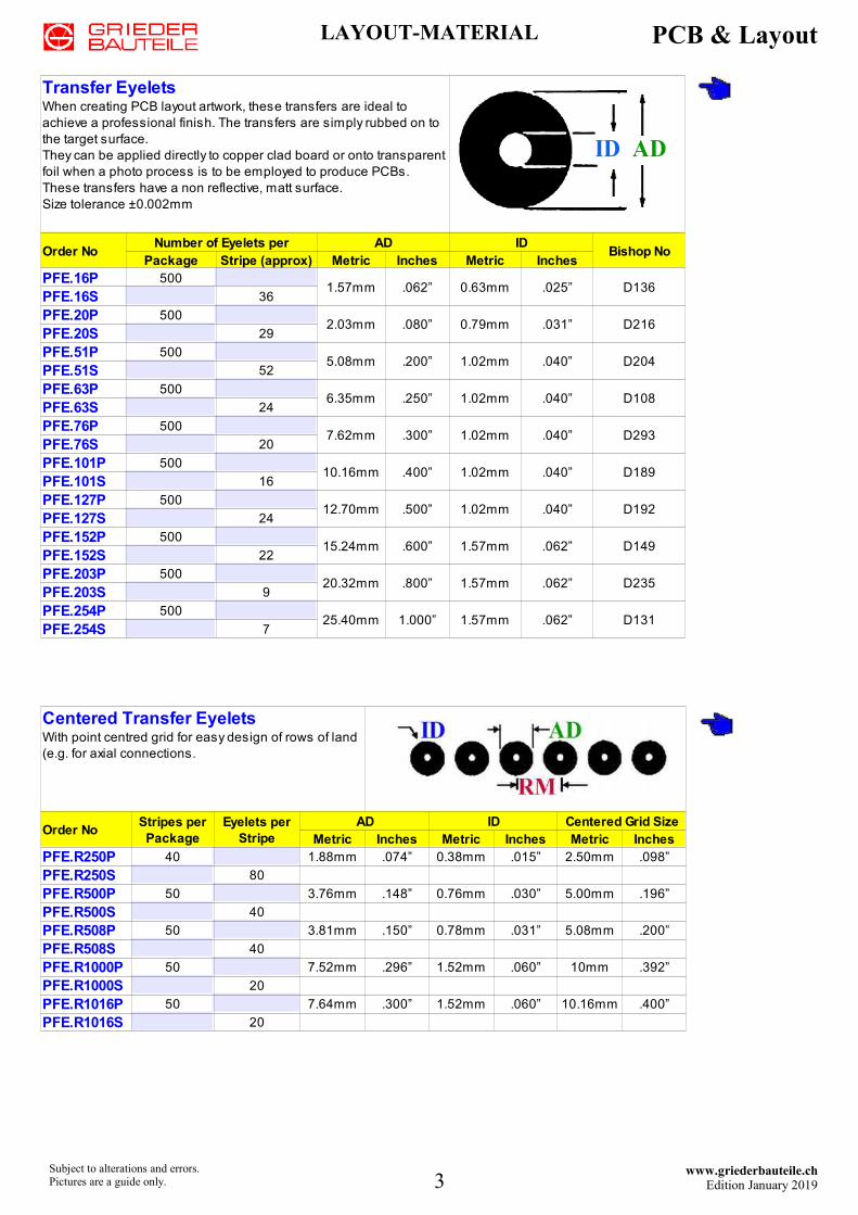
Transfer EyeletsWhen creating PCB layout artwork, these transfers are ideal to achieve a professional finish. The transfers are simply rubbed on to the target surface. They can be applied directly to copper clad board or onto transparent foil when a photo process is to be employed to produce PCBs. These transfers have a non reflective, matt surface.Size tolerance ±0.002mm
ID AD
Order NoAD ID Centered Grid Size
Metric Inches Metric Inches Metric InchesPFE.R250P 40 1.88mm .074” 0.38mm .015” 2.50mm .098”
PFE.R250S 80
PFE.R500P 50 3.76mm .148” 0.76mm .030” 5.00mm .196”
PFE.R500S 40
PFE.R508P 50 3.81mm .150” 0.78mm .031” 5.08mm .200”
PFE.R508S 40
PFE.R1000P 50 7.52mm .296” 1.52mm .060” 10mm .392”
PFE.R1000S 20
PFE.R1016P 50 7.64mm .300” 1.52mm .060” 10.16mm .400”
PFE.R1016S 20
Centered Transfer EyeletsWith point centred grid for easy design of rows of land (e.g. for axial connections.
Stripes per Package
Eyelets per Stripe
LAYOUT-MATERIAL
4
PCB & Layout
www.griederbauteile.chEdition January 2019
Subject to alterations and errors.Pictures are a guide only.
Order NoRow Spacing A
ScaleMetric Inches
PFD.163N1P 250 7.62mm .300” 4.45mm 16 1 : 1
PFD.163N2P 25015.24mm .600” 8.90mm 16 2 : 1
PFD.163N2E 1
PFD.203N1P 2507.62mm .300” 4.45mm 20 1 : 1
PFD.203N1E 1
PFD.203N2P 25015.24mm .600” 8.90mm 20 2 : 1
PFD.203N2E 1
PFD.224N1P 10010.16mm .400” 6.99mm 22 1 : 1
PFD.224N1E 1
PFD.224N2P 10020.32mm .800” 13.98mm 22 2 : 1
PFD.224N2E 1
PFD.246N1P 10015.24mm .600” 12.06mm 24 1 : 1
PFD.246N1E 1
PFD.246N2P 10030.48mm 1.200” 24.12mm 24 2 : 1
PFD.246N2E 1
PFD.406N1P 10015.24mm .600” 12.06mm 40 1 : 1
PFD.406N1E 1
PFD.406N2P 10030.48mm 1.200” 24.12mm 40 2 : 1
PFD.406N2E 1
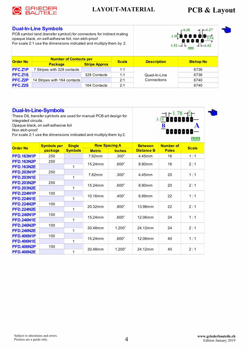
Dual-In-Line-SymbolsThese DIL transfer symbols are used for manual PCB art design for integrated circuits.Opaque black, on self-adhesive foilNon etch-proofFor scale 2:1 use the dimensions indicated and multiply them by 2.
Symbols per package
Single Symbols
Between Distance B
Number of Poles
Order NoNumber of Contacts per
Scale Description Bishop NoPackage Stripe Approx
PFC.Z1P 7 Stripes with 328 contacts 1:1 6736
PFC.Z1S 328 Contacts 1:1 6736
PFC.Z2P 14 Stripes with 164 contacts 2:1 6740
PFC.Z2S 164 Contacts 2:1 6740
Dual-In-Line SymbolsPCB symbol land (transfer symbol) for connectors for indirect matingopaque black, on self-adhesive foil, non etch-proofFor scale 2:1 use the dimensions indicated and multiply them by 2.
Quad-In-Line Connections
LAYOUT-MATERIAL
5
PCB & Layout
www.griederbauteile.chEdition January 2019
Subject to alterations and errors.Pictures are a guide only.
Order NoRow Spacing A
ScaleMetric Inches
PFD.163Z1P 2507.62mm .300” 4.45mm 16 1 : 1
PFD.163Z1E 1
PFD.163Z2P 25015.24mm .600” 8.90mm 16 2 : 1
PFD.163Z2E 1
PFD.246Z1P 10015.24mm .600” 12.06mm 24 1 : 1
PFD.246Z1E 1
PFD.246Z2P 10030.48mm 1.200” 24.12mm 24 2 : 1
PFD.246Z2E 1
PFD.406Z1P 10015.24mm .600” 12.06mm 40 1 : 1
PFD.406Z1E 1
PFD.406Z2P 10030.48mm 1.200” 24.12mm 40 2 : 1
PFD.406Z2E 1
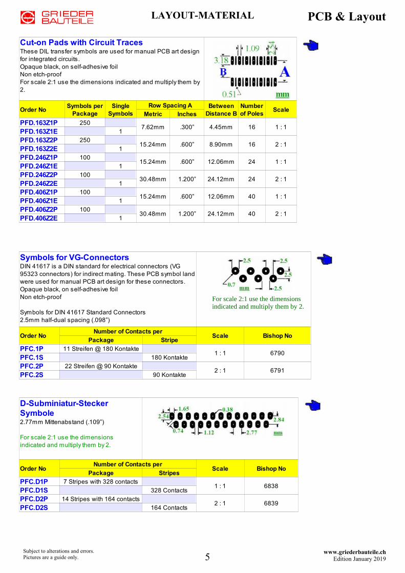
Cut-on Pads with Circuit TracesThese DIL transfer symbols are used for manual PCB art design for integrated circuits.Opaque black, on self-adhesive foilNon etch-proofFor scale 2:1 use the dimensions indicated and multiply them by 2.
Symbols per Package
Single Symbols
Between Distance B
Number of Poles
Order NoNumber of Contacts per
Scale Bishop NoPackage Stripe
PFC.1P 11 Streifen @ 180 Kontakte1 : 1 6790
PFC.1S 180 Kontakte
PFC.2P 22 Streifen @ 90 Kontakte2 : 1 6791
PFC.2S 90 Kontakte
Symbols for VG-ConnectorsDIN 41617 is a DIN standard for electrical connectors (VG 95323 connectors) for indirect mating. These PCB symbol land were used for manual PCB art design for these connectors. Opaque black, on self-adhesive foilNon etch-proof
Symbols for DIN 41617 Standard Connectors2.5mm half-dual spacing (.098”)
For scale 2:1 use the dimensions indicated and multiply them by 2.
Order NoNumber of Contacts per
Scale Bishop NoPackage Stripes
PFC.D1P 7 Stripes with 328 contacts1 : 1 6838
PFC.D1S 328 Contacts
PFC.D2P 14 Stripes with 164 contacts2 : 1 6839
PFC.D2S 164 Contacts
D-Subminiatur-Stecker Symbole2.77mm Mittenabstand (.109”)
For scale 2:1 use the dimensions indicated and multiply them by 2.
LAYOUT-MATERIAL
6
PCB & Layout
www.griederbauteile.chEdition January 2019
Subject to alterations and errors.Pictures are a guide only.
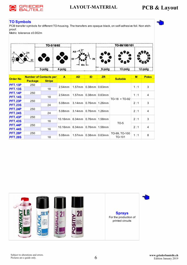
Order NoNumber of Contacts per A AD ID ZR
SuitableM Poles
Package Stripe
PFT.13P 2502.54mm 1.57mm 0.38mm 0.63mm
TO-18 + TO-92
1 : 1 3PFT.13S 18
PFT.14P 2502.54mm 1.57mm 0.38mm 0.63mm 1 : 1 4
PFT.14S 18
PFT.23P 2505.08mm 3.14mm 0.76mm 1.26mm 2 : 1 3
PFT.23S 24
PFT.24P 2505.08mm 3.14mm 0.76mm 1.26mm 2 : 1 4
PFT.24S 24
PFT.43P 25010.16mm 6.34mm 0.76mm 1.58mm
TO-5
2 : 1 3PFT.43S 16
PFT.44P 25010.16mm 6.34mm 0.76mm 1.58mm 2 : 1 4
PFT.44S 16
PFT.28P 2505.08mm 1.57mm 0.38mm 0.63mm 1 : 1 8
PFT.28S 18
TO SymbolsPCB transfer symbols for different TO-housing. The transfers are opaque black, on self-adhesive foil. Non etch-proof.Metric tolerance ±0.002m
TO-99, TO-100 TO-101
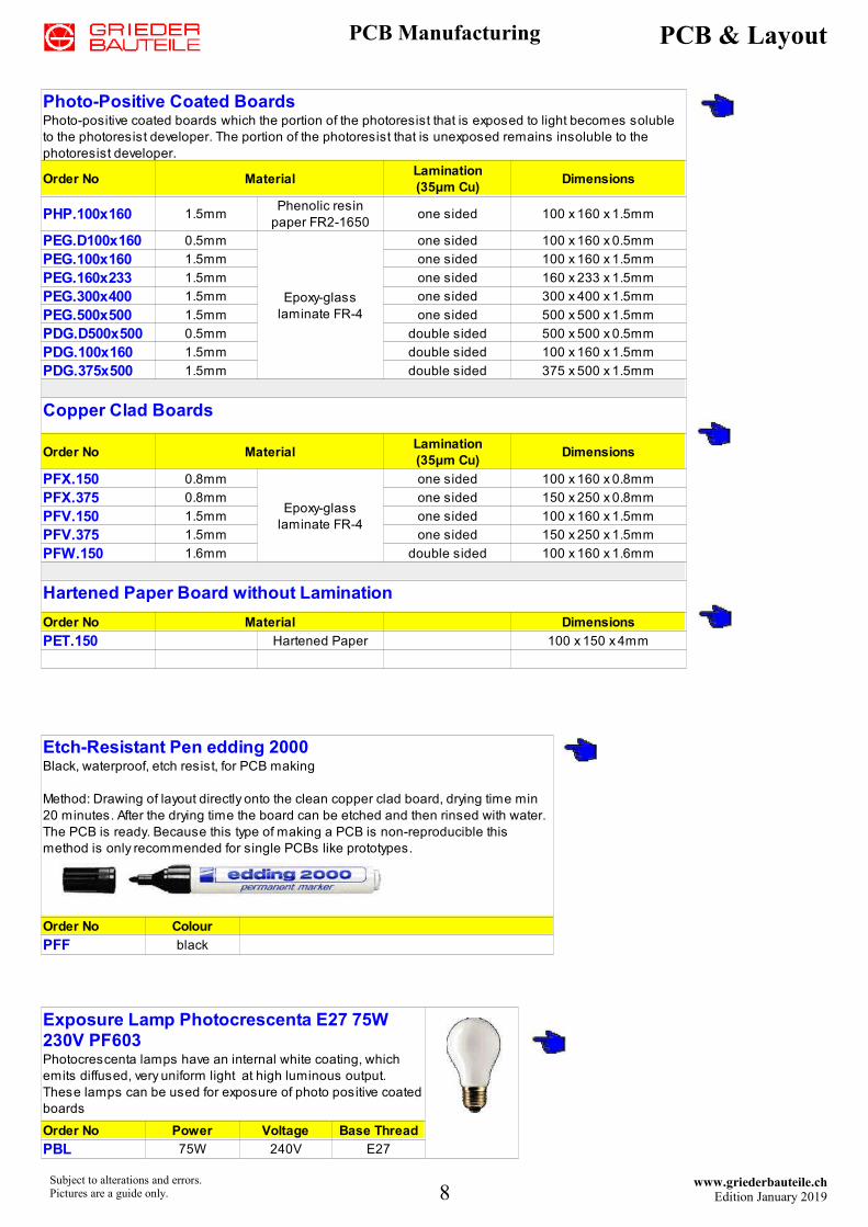
SpraysFor the production of
printed circuits
LAYOUT-MATERIAL
7
PCB & Layout
www.griederbauteile.chEdition January 2019
Subject to alterations and errors.Pictures are a guide only.
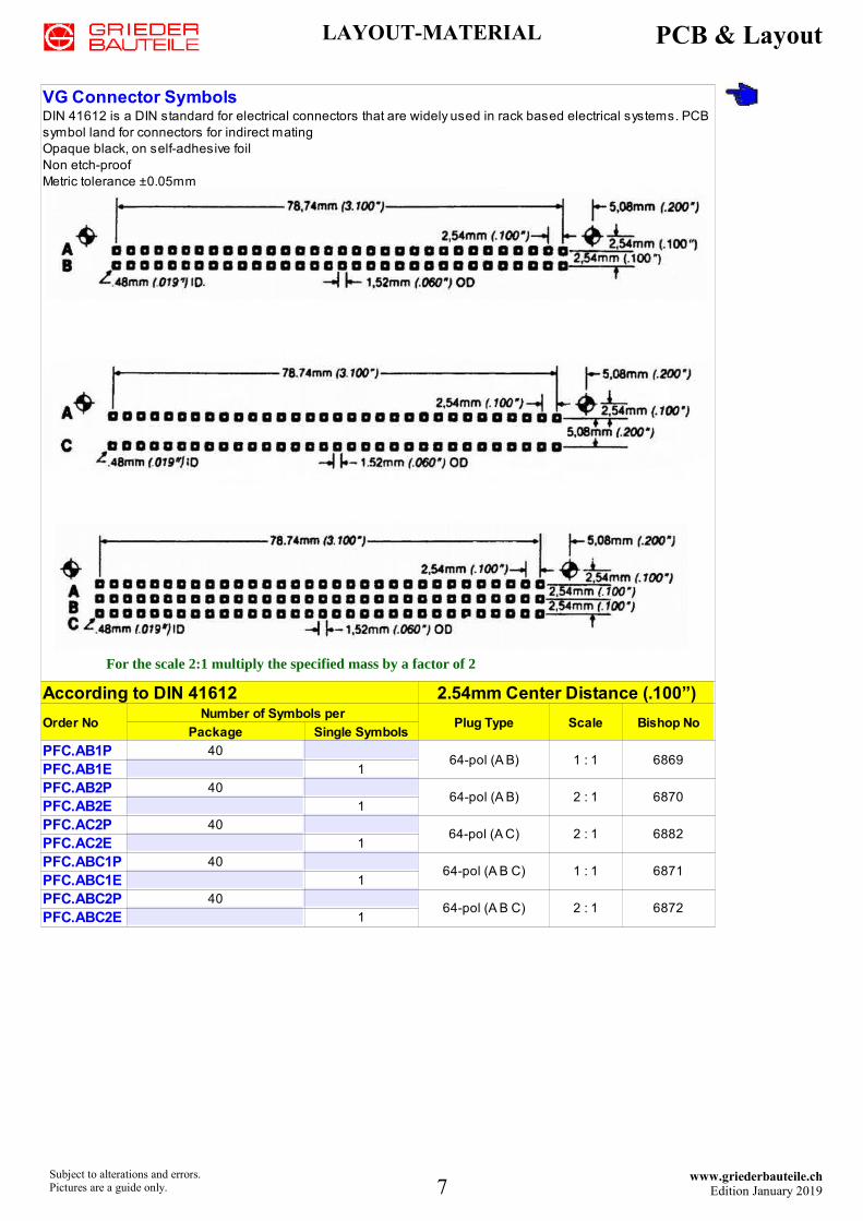
According to DIN 41612 2.54mm Center Distance (.100”)
Order NoNumber of Symbols per
Plug Type Scale Bishop NoPackage Single Symbols
PFC.AB1P 4064-pol (A B) 1 : 1 6869
PFC.AB1E 1
PFC.AB2P 4064-pol (A B) 2 : 1 6870
PFC.AB2E 1
PFC.AC2P 4064-pol (A C) 2 : 1 6882
PFC.AC2E 1
PFC.ABC1P 4064-pol (A B C) 1 : 1 6871
PFC.ABC1E 1
PFC.ABC2P 4064-pol (A B C) 2 : 1 6872
PFC.ABC2E 1
VG Connector SymbolsDIN 41612 is a DIN standard for electrical connectors that are widely used in rack based electrical systems. PCB symbol land for connectors for indirect matingOpaque black, on self-adhesive foilNon etch-proofMetric tolerance ±0.05mm
For the scale 2:1 multiply the specified mass by a factor of 2
LAYOUT-MATERIAL
8
PCB & Layout
www.griederbauteile.chEdition January 2019
Subject to alterations and errors.Pictures are a guide only.
PCB Manufacturing
Order No Material Dimensions
PHP.100x160 1.5mm one sided 100 x 160 x 1.5mm
PEG.D100x160 0.5mm one sided 100 x 160 x 0.5mm
PEG.100x160 1.5mm one sided 100 x 160 x 1.5mm
PEG.160x233 1.5mm one sided 160 x 233 x 1.5mm
PEG.300x400 1.5mm one sided 300 x 400 x 1.5mm
PEG.500x500 1.5mm one sided 500 x 500 x 1.5mm
PDG.D500x500 0.5mm double sided 500 x 500 x 0.5mm
PDG.100x160 1.5mm double sided 100 x 160 x 1.5mm
PDG.375x500 1.5mm double sided 375 x 500 x 1.5mm
Copper Clad Boards
Order No Material Dimensions
PFX.150 0.8mm one sided 100 x 160 x 0.8mm
PFX.375 0.8mm one sided 150 x 250 x 0.8mm
PFV.150 1.5mm one sided 100 x 160 x 1.5mm
PFV.375 1.5mm one sided 150 x 250 x 1.5mm
PFW.150 1.6mm double sided 100 x 160 x 1.6mm
Hartened Paper Board without Lamination
Order No Material Dimensions
PET.150 Hartened Paper 100 x 150 x 4mm
Photo-Positive Coated BoardsPhoto-positive coated boards which the portion of the photoresist that is exposed to light becomes soluble to the photoresist developer. The portion of the photoresist that is unexposed remains insoluble to the photoresist developer.
Lamination(35µm Cu)
Phenolic resin paper FR2-1650
Epoxy-glass laminate FR-4
Lamination(35µm Cu)
Epoxy-glass laminate FR-4
Order No Colour
PFF black
Etch-Resistant Pen edding 2000Black, waterproof, etch resist, for PCB making
Method: Drawing of layout directly onto the clean copper clad board, drying time min 20 minutes. After the drying time the board can be etched and then rinsed with water. The PCB is ready. Because this type of making a PCB is non-reproducible this method is only recommended for single PCBs like prototypes.
Order No Power Voltage Base Thread
PBL 75W 240V E27
Exposure Lamp Photocrescenta E27 75W 230V PF603Photocrescenta lamps have an internal white coating, which emits diffused, very uniform light at high luminous output. These lamps can be used for exposure of photo positive coated boards
9
PCB & Layout
www.griederbauteile.chEdition January 2019
Subject to alterations and errors.Pictures are a guide only.
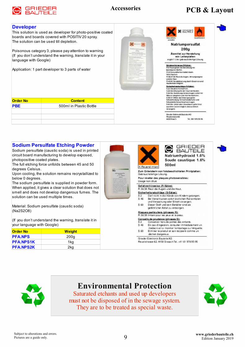
Order No Content
PBE 500ml in Plastic Bottle
DeveloperThis solution is used as developer for photo-positive coated boards and boards covered with POSITIV 20 spray.The solution can be used till depletion.
Poisonous category 3, please pay attention to warning(If you don’t understand the warning, translate it in your language with Google)
Application: 1 part developer to 3 parts of water
Order No Weight
PFA.NPS 200g
PFA.NPS1K 1kg
PFA.NPS2K 2kg
Sodium Persulfate Etching PowderSodium persulfate (caustic soda) is used in printed circuit board manufacturing to develop exposed, photopositive coated plates.The full etching force unfolds between 45 and 50 degrees Celsius.Upon cooling, the solution remains recrystallized to below 0 degrees.The sodium persulfate is supplied in powder form. When applied, it gives a clear solution that does not smell and does not develop dangerous fumes. The solution can be used multiple times.
Material: Sodium persulfate (caustic soda) (Na2S2O8)
(If you don’t understand the warning, translate it in your language with Google)
Accessories
Environmental ProtectionSaturated etchants and used up developers
must not be disposed of in the sewage system.They are to be treated as special waste.
10
PCB & Layout
www.griederbauteile.chEdition January 2019
Subject to alterations and errors.Pictures are a guide only.
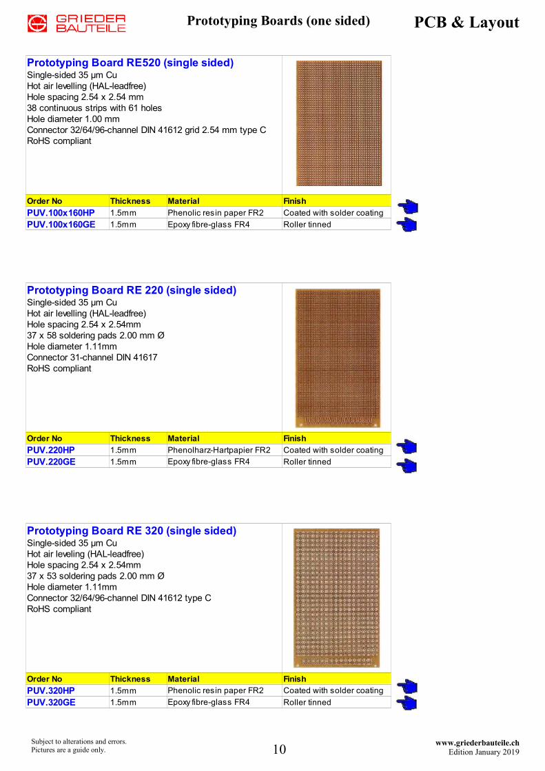
Order No Thickness Material Finish
PUV.100x160HP 1.5mm Phenolic resin paper FR2 Coated with solder coating
PUV.100x160GE 1.5mm Roller tinned
Prototyping Board RE520 (single sided)Single-sided 35 μm CuHot air levelling (HAL-leadfree)Hole spacing 2.54 x 2.54 mm38 continuous strips with 61 holesHole diameter 1.00 mmConnector 32/64/96-channel DIN 41612 grid 2.54 mm type CRoHS compliant
Epoxy fibre-glass FR4
Prototyping Boards (one sided)
Order No Thickness Material Finish
PUV.220HP 1.5mm Phenolharz-Hartpapier FR2 Coated with solder coating
PUV.220GE 1.5mm Epoxy fibre-glass FR4 Roller tinned
Prototyping Board RE 220 (single sided)Single-sided 35 μm CuHot air levelling (HAL-leadfree)Hole spacing 2.54 x 2.54mm37 x 58 soldering pads 2.00 mm ØHole diameter 1.11mmConnector 31-channel DIN 41617 RoHS compliant
Order No Thickness Material Finish
PUV.320HP 1.5mm Phenolic resin paper FR2 Coated with solder coating
PUV.320GE 1.5mm Epoxy fibre-glass FR4 Roller tinned
Prototyping Board RE 320 (single sided)Single-sided 35 μm CuHot air leveling (HAL-leadfree)Hole spacing 2.54 x 2.54mm37 x 53 soldering pads 2.00 mm ØHole diameter 1.11mmConnector 32/64/96-channel DIN 41612 type CRoHS compliant
11
PCB & Layout
www.griederbauteile.chEdition January 2019
Subject to alterations and errors.Pictures are a guide only.
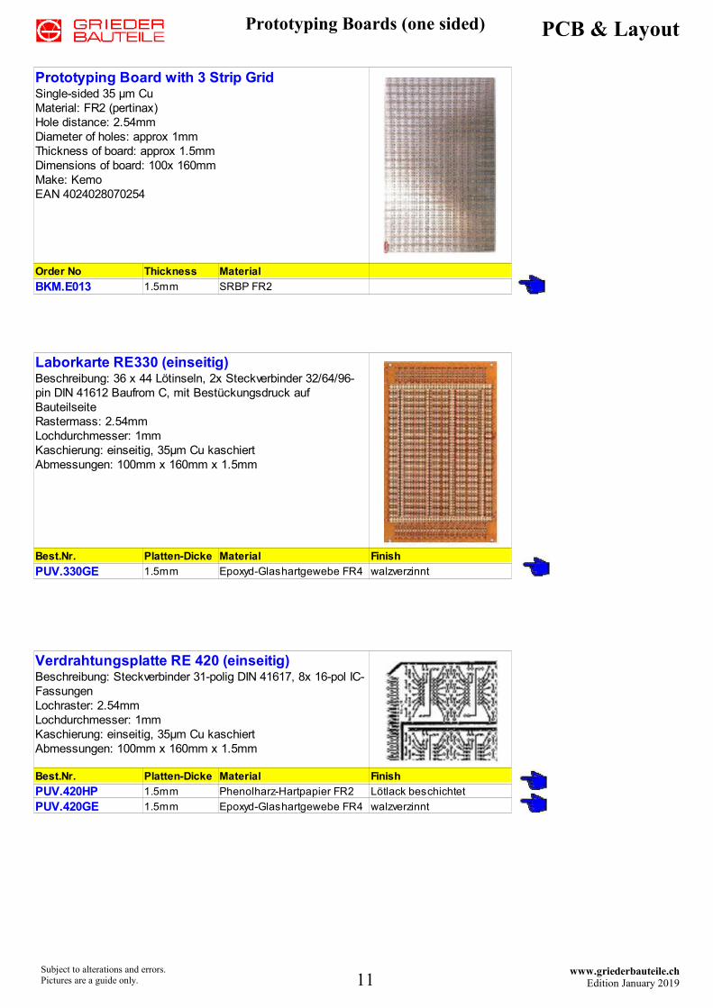
Order No Thickness Material
BKM.E013 1.5mm SRBP FR2
Prototyping Board with 3 Strip GridSingle-sided 35 μm CuMaterial: FR2 (pertinax)Hole distance: 2.54mmDiameter of holes: approx 1mmThickness of board: approx 1.5mmDimensions of board: 100x 160mmMake: KemoEAN 4024028070254
Best.Nr. Platten-Dicke Material Finish
PUV.330GE 1.5mm Epoxyd-Glashartgewebe FR4 walzverzinnt
Laborkarte RE330 (einseitig)Beschreibung: 36 x 44 Lötinseln, 2x Steckverbinder 32/64/96-pin DIN 41612 Baufrom C, mit Bestückungsdruck auf BauteilseiteRastermass: 2.54mmLochdurchmesser: 1mmKaschierung: einseitig, 35µm Cu kaschiertAbmessungen: 100mm x 160mm x 1.5mm
Best.Nr. Platten-Dicke Material Finish
PUV.420HP 1.5mm Phenolharz-Hartpapier FR2
PUV.420GE 1.5mm Epoxyd-Glashartgewebe FR4 walzverzinnt
Verdrahtungsplatte RE 420 (einseitig)Beschreibung: Steckverbinder 31-polig DIN 41617, 8x 16-pol IC-FassungenLochraster: 2.54mmLochdurchmesser: 1mmKaschierung: einseitig, 35µm Cu kaschiertAbmessungen: 100mm x 160mm x 1.5mm
Lötlack beschichtet
Prototyping Boards (one sided)
12
PCB & Layout
www.griederbauteile.chEdition January 2019
Subject to alterations and errors.Pictures are a guide only.
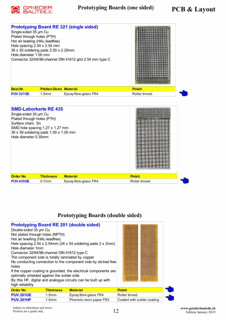
Best.Nr. Platten-Dicke Material Finish
PUV.321GE 1.5mm Epoxy fibre-glass FR4 Roller tinned
Prototyping Board RE 321 (single sided)Single-sided 35 μm CuPlated through holes (PTH)Hot air leveling (HAL-leadfree)Hole spacing 2.54 x 2.54 mm36 x 55 soldering pads 2.00 x 2.20mmHole diameter 1.00 mmConnector 32/64/96-channel DIN 41612 grid 2.54 mm type C
Order No Thickness Material Finish
PUV.201GE 1.5mm Epoxy fibre-glass FR4 Roller tinned
PUV.201HP 1.5mm Phenolic resin paper FR2 Coated with solder coating
Prototyping Board RE 201 (double sided)Double-sided 35 μm CuNot plated through holes (NPTH)Hot air levelling (HAL-leadfree)Hole spacing 2.54 x 2.54mm (34 x 54 soldering pads 2 x 2mm)Hole diameter 1mmConnector 32/64/96-channel DIN 41612 type CThe component side is totally laminated by copperNo conducting connection to the component side by etched free holesIf the copper coating is grounded, the electrical components are optimally shielded against the solder sideBy this HF, digital and analogue circuits can be built up with high reliability
Order No Thickness Material Finish
PUV.435GE 0.7mm Epoxy fibre-glass FR4 Roller tinned
SMD-Laborkarte RE 435Single-sided 35 μm CuPlated through holes (PTH)Surface chem. SnSMD hole spacing 1.27 x 1.27 mm39 x 59 soldering pads 1.00 x 1.00 mmHole diameter 0.30mm
Prototyping Boards (one sided)
Prototyping Boards (double sided)

13
PCB & Layout
www.griederbauteile.chEdition January 2019
Subject to alterations and errors.Pictures are a guide only.
Order No Thickness Material Finish
PUV.436GE 1.5mm Epoxy fibre-glass FR4 Roller tinned
SMD-Bread Board RE 436 (double sided)Double-sided 35 μm CuPlated through holes (PTH)Surface chem. SnSMD hole spacing 1.27 x 1.27 mm39 x 59 soldering pads 1.00 x 1.00 mmHole diameter 0.30mmDimension board: 100mm x 160mm x 1.5mm
Order No Thickness Material Finish
PUV.440PGA 1.5mm Epoxy fibre-glass FR4 Roller tinned
PGA-Prototyping Board RE 440 (double sided)Double-sided 35 μm CuPlated through holes (PTH)Hot air leveling (HAL-leadfree)Surface with soldering stop maskStaggered hole grid 2.54 x 2.54mm, thus duplication of the borings (interstitial)Soldering pads 1.4mm Ø4304 holes 0.8mm ØParticulary appropriate for PGA sockets in staggered grid 2.54 x 2.54mmConnector 32/64/96-channel DIN 41612 type CWorking temperature max. 150°CSolder bath proof: 260°C > 50 Sec.
Order No
PGL.301
Solderless Breadboard (270 Tie-point) EIC-301Tie-points: 270Dimensions: 84 x 45 x 8.5mm
Bread Boards
Prototyping Boards (double sided)
14
PCB & Layout
www.griederbauteile.chEdition January 2019
Subject to alterations and errors.Pictures are a guide only.
Order No
PGL.404
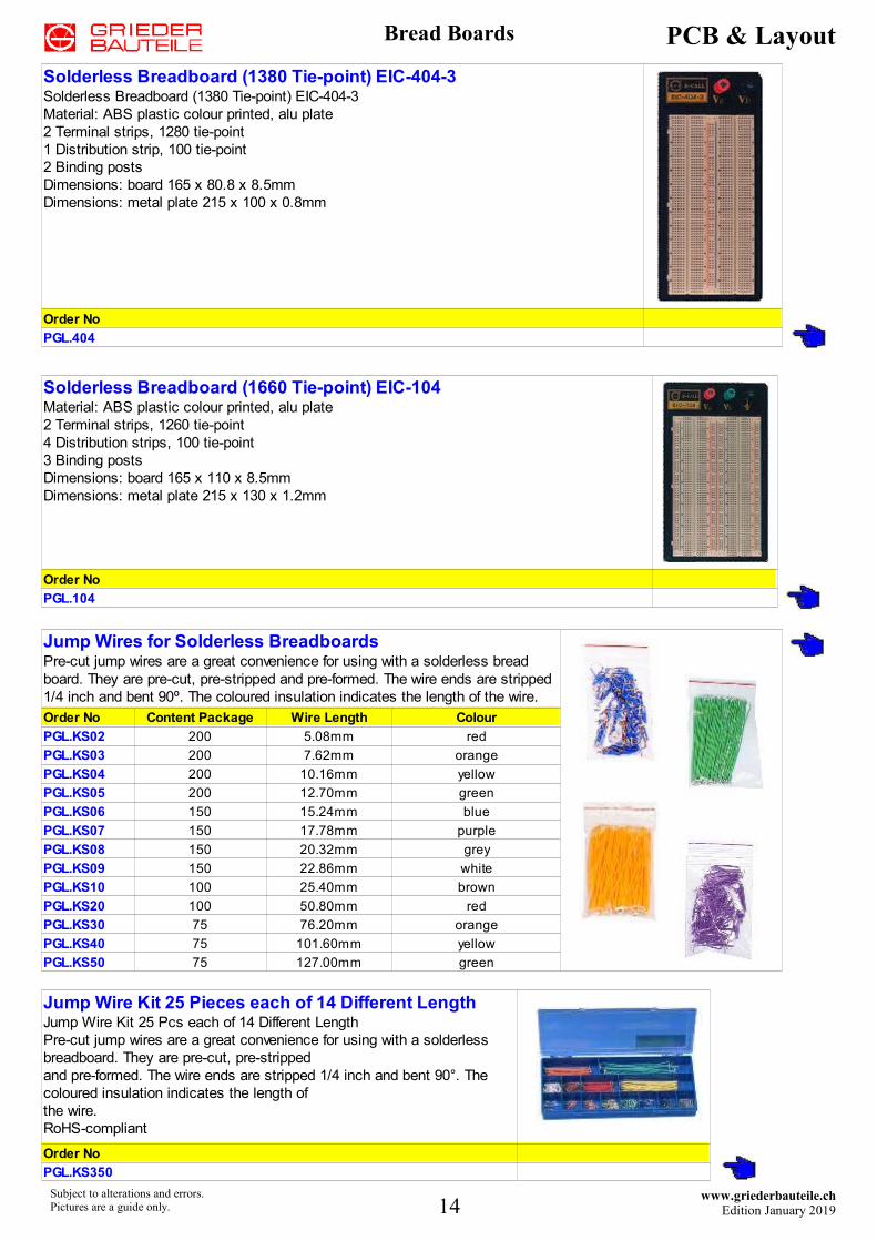
Solderless Breadboard (1380 Tie-point) EIC-404-3Solderless Breadboard (1380 Tie-point) EIC-404-3Material: ABS plastic colour printed, alu plate2 Terminal strips, 1280 tie-point1 Distribution strip, 100 tie-point2 Binding postsDimensions: board 165 x 80.8 x 8.5mmDimensions: metal plate 215 x 100 x 0.8mm
Order No
PGL.104
Solderless Breadboard (1660 Tie-point) EIC-104Material: ABS plastic colour printed, alu plate2 Terminal strips, 1260 tie-point4 Distribution strips, 100 tie-point3 Binding postsDimensions: board 165 x 110 x 8.5mmDimensions: metal plate 215 x 130 x 1.2mm
Bread Boards
Order No
PGL.KS350
Jump Wire Kit 25 Pieces each of 14 Different LengthJump Wire Kit 25 Pcs each of 14 Different LengthPre-cut jump wires are a great convenience for using with a solderless breadboard. They are pre-cut, pre-stripped and pre-formed. The wire ends are stripped 1/4 inch and bent 90°. The coloured insulation indicates the length of the wire.RoHS-compliant
Order No Content Package Wire Length Colour
PGL.KS02 200 5.08mm red
PGL.KS03 200 7.62mm orange
PGL.KS04 200 10.16mm yellow
PGL.KS05 200 12.70mm green
PGL.KS06 150 15.24mm blue
PGL.KS07 150 17.78mm purple
PGL.KS08 150 20.32mm grey
PGL.KS09 150 22.86mm white
PGL.KS10 100 25.40mm brown
PGL.KS20 100 50.80mm red
PGL.KS30 75 76.20mm orange
PGL.KS40 75 101.60mm yellow
PGL.KS50 75 127.00mm green
Jump Wires for Solderless BreadboardsPre-cut jump wires are a great convenience for using with a solderless bread board. They are pre-cut, pre-stripped and pre-formed. The wire ends are stripped 1/4 inch and bent 90º. The coloured insulation indicates the length of the wire.