low voltage clocking methodologies for nanoscale icsemre/papers/phdthesis_liu.pdf · a slew...
TRANSCRIPT
Low Voltage Clocking Methodologies for Nanoscale ICs
A Dissertation Presented
by
Weicheng Liu
to
The Graduate School
in Partial Fulfillment of the
Requirements
for the Degree of
Doctor of Philosophy
in
Electrical Engineering
Stony Brook University
January 2018

Stony Brook University
The Graduate School
Weicheng Liu
We the dissertation committee for the above candidate for theDoctor of Philosophy degree,
hereby recommend acceptance of this dissertation.
Dr. Emre Salman - Advisor of DissertationAssociate Professor, Department of Electrical and Computer Engineering
Dr. Alex Doboli - Chairperson of DefenseProfessor, Department of Electrical and Computer Engineering
Dr. Peter Milder - Defense Committee MemberAssistant Professor, Department of Electrical and Computer Engineering
Dr. Milutin Stanacevic - Defense Committee MemberAssociate Professor, Department of Electrical and Computer Engineering
Dr. Mike Ferdman - Defense Committee MemberAssistant Professor, Department of Computer Science
Dr. Savithri Sundareswaran - Defense Committee MemberPrincipal Engineer, NXP Semiconductors
This dissertation is accepted by the Graduate School
Charles TaberDean of the Graduate School
Abstract of the Dissertation
Low Voltage Clocking Methodologies for Nanoscale ICs
by
Weicheng Liu
Doctor of Philosophy
in
Electrical Engineering
Stony Brook University
2018
Power consumption has emerged as a key design objective for almost any ap-
plication. Low swing/voltage clock distribution was proposed in earlier work as
a method to reduce power consumption since clock networks typically consume
a significant portion of the overall dynamic power in synchronous integrated cir-
cuits (ICs). Existing works on low voltage clocking, however, suffer from multiple
issues, making these approaches impractical for industrial circuits. For example,
most of the existing studies sacrifice performance when lowering the supply voltage
of a clock network, such as clock networks developed for near-threshold comput-
ing. The primary objective of this dissertation is to develop a low voltage clocking
methodology without degrading circuit performance (operating frequency) or clock
network characteristics (such as skew and slew). This objective is achieved through
iii
several circuit and algorithmic innovations.
A novel D flip-flop (DFF) cell that can reliably operate with a low voltage
clock signal and a nominal voltage data signal is proposed. Contrary to existing
approaches where the last stage of the clock network operates at nominal voltage,
the proposed cell enables low voltage clock operation throughout the entire clock
network, thereby maximizing power savings. Furthermore, a similar clock-to-Q de-
lay is maintained to satisfy the same timing constraints. Simulation results demon-
strate that when the clock voltage is scaled to 70% of the nominal supply voltage,
the proposed DFF cell achieves up to 53% power savings at the expense of approx-
imately 50% increase in cell-level physical area. At chip-level, the increase in area
is approximately 15%.
At low supply voltages, satisfying the slew constraint becomes highly chal-
lenging due to reduced drive ability of the clock buffers. A slew driven-clock tree
synthesis (CTS) methodology, referred to as SLECTS, is proposed to satisfy tight
slew constraints at scaled supply voltages. Contrary to existing CTS methods that
are primarily delay/skew based and slew is considered only during post-CTS op-
timization, in the proposed approach, slew constraint is integrated into the critical
steps of the synthesis process (such as merging clock tree nodes, defining routing
points, and handling long interconnects). For an industrial 4-core application pro-
iv

cessor with approximately 1 million gates and implemented in 28 nm fully depleted
silicon-on-insulator (FD-SOI) CMOS technology, the proposed slew-driven CTS
methodology achieves up to 15% reduction in clock tree power while producing
satisfactory skew and slew characteristics. Furthermore, contrary to the vendor tool
that exhibits slew violations, the proposed approach satisfies tight slew constraints.
When the proposed DFF cell is combined with the proposed CTS methodology, up
to 48% reduction in overall clocking power is achieved under similar performance
constraints at the expense of 15% increase in area.
In clock trees with highly aggressive design constraints, selective low voltage
clocking was considered to satisfy the tight constraints. A novel level-up shifter
with dual supply voltage is proposed to enable such operation. Simulation results
demonstrate that the proposed level shifter achieves 43% and 36% reduction in, re-
spectively, transient power and leakage power as compared to a conventional cross-
coupled level shifter, while consuming 9.5% less physical area.
Clock gating is an effective and common technique to reduce the switching
power of the clock networks. Clock signals arrive at clock gating cells earlier than
sinks, which reduces the timing slack of Enable paths. A useful skew methodol-
ogy for gated low voltage clock trees is proposed to relax the timing constraints of
Enable paths. The methodology is evaluated using the largest ISCAS’89 bench-
v

mark circuits. The results demonstrate an average 47% increase in the timing slack
of the Enable path.
The design methodologies proposed in this dissertation facilitate low voltage
clocking for high performance industrial circuits. Significant reduction in clock
power is achieved without degrading clock frequency and primary clock constraints
such as skew and slew. The proposed methodologies were integrated into a conven-
tional design flow and demonstrated using large scale industrial circuits.
vi

Table of Contents
Abstract vi
List of Figures xiii
List of Tables xiv
Acknowledgements xvi
1 Introduction 1
2 Background 42.1 Clock Distribution Networks . . . . . . . . . . . . . . . . . . . . . 5
2.1.1 Clock Tree Topologies . . . . . . . . . . . . . . . . . . . . 72.1.1.1 Buffered Clock Trees . . . . . . . . . . . . . . . 72.1.1.2 H-trees . . . . . . . . . . . . . . . . . . . . . . . 9
2.1.2 Clock Skew . . . . . . . . . . . . . . . . . . . . . . . . . . 112.1.3 Timing Constraints Considering Clock Skew . . . . . . . . 122.1.4 Clock Tree Synthesis (CTS) . . . . . . . . . . . . . . . . . 17
2.2 Existing Works on Low Voltage Clocking . . . . . . . . . . . . . . 192.3 Primary Challenges in Developing a Low Voltage Clock Network . 20
2.3.1 Low Swing Operation at the Sinks: New Flip-Flop Cell . . . 212.3.2 Satisfy Skew and Slew Constraints: Novel CTS and Level
Shifter . . . . . . . . . . . . . . . . . . . . . . . . . . . . . 212.3.3 Degraded Enable Path Timing: Exploit Useful Skew . . . . 22
3 Flip-Flop Design to Facilitate Low Swing Operation 243.1 Effect of Low Swing Operation on Flip-Flop . . . . . . . . . . . . . 25
3.1.1 Reliability . . . . . . . . . . . . . . . . . . . . . . . . . . . 253.1.2 Power Consumption . . . . . . . . . . . . . . . . . . . . . 27
vii

3.2 Existing Low Swing Flip-Flops . . . . . . . . . . . . . . . . . . . . 283.3 Proposed D-Flip-Flop Topology for Low Swing Clocking . . . . . . 323.4 Simulation Results . . . . . . . . . . . . . . . . . . . . . . . . . . 34
3.4.1 Comparison with Conventional Full Swing Flip-flop . . . . 343.4.2 Comparison with Existing Low Swing Flip-flops . . . . . . 38
3.4.2.1 Comparative Analysis . . . . . . . . . . . . . . . 393.4.2.2 Robustness to Variations . . . . . . . . . . . . . . 42
3.5 Summary . . . . . . . . . . . . . . . . . . . . . . . . . . . . . . . 44
4 Level Shifter for Selective Low Swing Clocking 454.1 Cross-Coupled Topology . . . . . . . . . . . . . . . . . . . . . . . 474.2 Bootstrapping Technique . . . . . . . . . . . . . . . . . . . . . . . 484.3 Proposed Level Shifter for Selective Low Swing Clocking . . . . . 494.4 Simulation Results . . . . . . . . . . . . . . . . . . . . . . . . . . 51
4.4.1 Power-Delay Product . . . . . . . . . . . . . . . . . . . . . 524.4.2 Nominal and Corner Simulation Results . . . . . . . . . . . 534.4.3 Dependence on Input Swing . . . . . . . . . . . . . . . . . 554.4.4 Area Comparison . . . . . . . . . . . . . . . . . . . . . . . 55
4.5 Summary . . . . . . . . . . . . . . . . . . . . . . . . . . . . . . . 56
5 Exploiting Useful Skew in Gated Low Voltage Clock Trees for HighPerformance 585.1 Background on Low Swing Operation and Problem Formulation . . 60
5.1.1 Traditional Clock Skew Scheduling . . . . . . . . . . . . . 615.1.2 Clock Skew Scheduling with Clock Gating . . . . . . . . . 645.1.3 Low Swing Operation . . . . . . . . . . . . . . . . . . . . 66
5.2 Proposed Approach . . . . . . . . . . . . . . . . . . . . . . . . . . 685.2.1 Maximizing Circuit Performance . . . . . . . . . . . . . . 68
5.2.1.1 Linear Programming . . . . . . . . . . . . . . . . 685.2.1.2 Constraint Graph . . . . . . . . . . . . . . . . . 70
5.2.2 Increasing Timing Slack of EEEnnnaaabbbllleee Paths . . . . . . . . . . 745.3 Experimental Results . . . . . . . . . . . . . . . . . . . . . . . . . 75
5.3.1 Circuit Performance . . . . . . . . . . . . . . . . . . . . . 755.3.2 Timing Slack of EEEnnnaaabbbllleee Paths . . . . . . . . . . . . . . . . 78
5.4 Summary . . . . . . . . . . . . . . . . . . . . . . . . . . . . . . . 79
viii

6 Slew-Driven Clock Tree Synthesis Methodology 816.1 Slew-Driven Clock Tree Synthesis Algorithm . . . . . . . . . . . . 84
6.1.1 Step 1: Merging Point Computation . . . . . . . . . . . . . 846.1.2 Step 2: Fixing Skew Using Buffer Insertion . . . . . . . . . 906.1.3 Step 3: Fixing Slew Using Buffer Sizing . . . . . . . . . . . 926.1.4 Step 4: Finding Feasible Pairs to Merge . . . . . . . . . . . 936.1.5 Step 5: Slew-Aware Net Splitting . . . . . . . . . . . . . . 966.1.6 Runtime and Computational Complexity . . . . . . . . . . 98
6.2 Experimental Results on an Industrial Processor . . . . . . . . . . . 996.2.1 Results at the Slowest Corner . . . . . . . . . . . . . . . . 1026.2.2 Results at Scaled Voltages . . . . . . . . . . . . . . . . . . 105
6.3 SLECTS with the Low Swing Flip-Flop . . . . . . . . . . . . . . . 1076.3.1 ISCAS’89 Benchmark s38584 . . . . . . . . . . . . . . . . 1096.3.2 64-point FFT Core . . . . . . . . . . . . . . . . . . . . . . 111
6.4 Summary . . . . . . . . . . . . . . . . . . . . . . . . . . . . . . . 112
7 Conclusion and Future Directions 1147.1 Thesis Summary . . . . . . . . . . . . . . . . . . . . . . . . . . . 1147.2 Future Directions . . . . . . . . . . . . . . . . . . . . . . . . . . . 116
Bibliography 118
ix

List of Figures
1.1 Primary components of the proposed low swing clocking method-ology. . . . . . . . . . . . . . . . . . . . . . . . . . . . . . . . . . 3
2.1 A simple synchronous system. . . . . . . . . . . . . . . . . . . . . 52.2 An example of a buffered clock tree. . . . . . . . . . . . . . . . . . 82.3 An example of a clock tree after synthesis. . . . . . . . . . . . . . . 92.4 An example of a symmetric H-tree. . . . . . . . . . . . . . . . . . . 102.5 A typical data path. . . . . . . . . . . . . . . . . . . . . . . . . . . 112.6 Positive and negative clock skews. . . . . . . . . . . . . . . . . . . 122.7 Two sequentially adjacent registers. . . . . . . . . . . . . . . . . . 132.8 Flip-flop max delay constraint with zero clock skew. . . . . . . . . 132.9 Flip-flop max delay constraint with positive clock skew. . . . . . . . 142.10 Flip-flop min delay constraint with zero clock skew. . . . . . . . . . 152.11 Flip-flop min delay constraint with negative clock skew. . . . . . . . 162.12 An abstract tree. . . . . . . . . . . . . . . . . . . . . . . . . . . . . 182.13 A simplified gated clock network consisting of five sinks, an inte-
grated clock gating (ICG) cell, and an Enable path. . . . . . . . . . 22
3.1 A typical transmission gate based D flip-flop topology driven by alow swing clock signal. . . . . . . . . . . . . . . . . . . . . . . . . 26
3.2 Increase in power consumption when a conventional DFF is drivenwith a low swing clock signal while the clock sub-circuit is con-nected to a nominal VDD. . . . . . . . . . . . . . . . . . . . . . . . 28
3.3 Existing low swing flip-flop topologies (a)C2MOS and sense amplifier based lowswing flip-flop, L-C2MOS-SA [1], (b)reduced clock swing flip-flop, RCSFF [2],(c)NAND-type keeper flip-flop, NDKFF [3], and (d)contention reduced flip-flop,CRFF [4]. . . . . . . . . . . . . . . . . . . . . . . . . . . . . . . . . 29
x

3.4 Proposed DFF topology that can reliably work with a low swingclock signal whereas the data and output signals are at full swing,(a) schematic, (b) layout in the 45 nm technology. . . . . . . . . . . 33
3.5 Correct functionality of the proposed low swing DFF cell in 32 nmtechnology: (a) latching logic-low, (b) latching logic-high. . . . . . 34
3.6 Power consumption comparison of the proposed low swing DFFcell (LSDFF) with the conventional full swing DFF cell (FSDFF):(a) 45 nm technology, (b) 32 nm technology. . . . . . . . . . . . . . 35
3.7 Clock-to-Q delay comparison of the proposed low swing DFF cell(LSDFF) with the conventional full swing DFF cell (FSDFF): (a)45 nm technology, (b) 32 nm technology. . . . . . . . . . . . . . . 36
3.8 Effect of clock swing voltage level on clock-to-Q delay and powerconsumption for each flip-flop topology: (a) Clock-to-Q delay vs.clock voltage swing, (b) power consumption vs. clock voltage swing. 41
4.1 Selective low swing clocking. . . . . . . . . . . . . . . . . . . . . . 464.2 Primary existing level shifters: (a) conventional cross-coupled topol-
ogy, (b) bootstrapping technique. . . . . . . . . . . . . . . . . . . . 484.3 Proposed level shifter (a) schematic, (b) physical layout. . . . . . . 504.4 Input and output waveforms of the proposed level shifter. . . . . . . 514.5 Power-delay product as a function of scale factor for each topology:
(a) cross-coupled, (b) bootstrapped, (c) buffer, (d) proposed. . . . . 534.6 Dependence on input supply voltage: (a) power as a function of
input supply voltage, (b) delay as a function of input supply voltage. 56
5.1 Simple sequential circuit consisting of three registers without clockgating. . . . . . . . . . . . . . . . . . . . . . . . . . . . . . . . . . 61
5.2 Constraint graph based formulation of skew scheduling for the cir-cuit shown in Fig. 5.1: (a) constraint graph, (b) after applying aclock period of 10 units eliminating all of the negative weight cycles. 63
5.3 Integrated clock gating (ICG) cell. . . . . . . . . . . . . . . . . . . 645.4 Simple sequential circuit consisting of an ICG cell, two registers
gated by this ICG cell, a local clock sub-tree, and a timing loopformed by clock propagation path and clock enable path. . . . . . . 65
5.5 Timing graph of the gated clock network shown in Fig. 2.13. . . . . 675.6 Simple example to illustrate the timing loop formed by an ICG cell
and a register gated by this ICG cell. . . . . . . . . . . . . . . . . . 71
xi

5.7 Constraint graph of the circuit shown in Fig. 5.6: (a) original graph,(b) after one iteration with clock period as 11 units, (c) after break-ing the timing loop. . . . . . . . . . . . . . . . . . . . . . . . . . . 71
5.8 Constraint graph of the circuit shown in Fig. 5.4: (a) original graph,(b) after one iteration with clock period as 22 units, (c) after break-ing the timing loop. . . . . . . . . . . . . . . . . . . . . . . . . . . 73
5.9 The runtime comparison of linear programming and graph basedapproaches. . . . . . . . . . . . . . . . . . . . . . . . . . . . . . . 78
6.1 The flowchart of SLECTS. The blue boxes are executed in everyf oreach loop, and the red boxes are executed after an iteration off oreach loop is finished. . . . . . . . . . . . . . . . . . . . . . . . 85
6.2 Permissible merging window and minimum slew point definitionsto identify the merging point. . . . . . . . . . . . . . . . . . . . . . 87
6.3 Illustration of fixing skew using single or multiple buffers and de-termining the new merging point after fixing skew. . . . . . . . . . 91
6.4 Demonstration of slew-aware net splitting. . . . . . . . . . . . . . . 966.5 Runtime comparison of SLECTS and a vendor tool for three circuits
described in Section 6.2. . . . . . . . . . . . . . . . . . . . . . . . 996.6 Illustration of the clock trees synthesized with SLECTS: (a) 64-
point FFT core floorplan, (b) Cortex A53 floorplan. . . . . . . . . . 1016.7 Power savings in clock tree achieved by SLECTS for both cases. . . 1056.8 The comparison of power dissipated by conventional full swing
flip-flop and the proposed low swing flip-flop as a function of clockswing. . . . . . . . . . . . . . . . . . . . . . . . . . . . . . . . . . 108
6.9 The comparison of the clock power of s38584 in two cases: (1)vendor tool synthesized clock tree with conventional full swing flip-flops at the nominal voltage, (2) SLECTS synthesized clock treewith the proposed low swing flip-flops at different clock swings. . . 109
6.10 The comparison of the clock power of s38584 at different clockswings. . . . . . . . . . . . . . . . . . . . . . . . . . . . . . . . . 110
6.11 The comparison of the clock power of 64-point FFT core in twocases: (1) vendor tool synthesized clock tree with conventional fullswing flip-flops at the nominal voltage, (2) SLECTS synthesizedclock tree with the proposed low swing flip-flops at different clockswings. . . . . . . . . . . . . . . . . . . . . . . . . . . . . . . . . 111
6.12 The comparison of the clock power of 64-point FFT core at differ-ent clock swings. . . . . . . . . . . . . . . . . . . . . . . . . . . . 112
xii

List of Tables
3.1 Setup and hold time simulation results of full swing DFF and theproposed low swing DFF at 45 and 32 nm technology nodes. . . . . 37
3.2 Corner simulation results of full swing DFF and the proposed lowswing DFF at 45 and 32 nm technology nodes. . . . . . . . . . . . . 38
3.3 Layout areas of full swing DFF and the proposed low swing DFFat 45 and 32 nm technology nodes. . . . . . . . . . . . . . . . . . . 38
3.4 Comparison of the proposed topology with existing work undernominal operating conditions with a clock voltage swing of 0.7×VDD.Each topology is sized to achieve approximately equal clock-to-Qdelay. . . . . . . . . . . . . . . . . . . . . . . . . . . . . . . . . . 40
3.5 Comparison of the proposed topology with existing work underworst-case operating conditions for clock-to-Q delay, overall tran-sient power, and leakage power. FF and SS correspond, respec-tively, to fast and slow models for both NMOS and PMOS transistors. 42
4.1 Extracted results at nominal corner. . . . . . . . . . . . . . . . . . . 544.2 Worst corner for delay (SS model, 0.9V supply and 165C) and
transient power (FF model, 1.1V supply and -40C) . . . . . . . . . 544.3 Worst corner for leakage (FF model, 1.1V supply and 165C) . . . . 55
5.1 LP based formulation of skew scheduling for the simple circuitshown in Fig. 5.1. . . . . . . . . . . . . . . . . . . . . . . . . . . . 62
5.2 LP based approach to clock skew scheduling in a clock gated design. 695.3 Application of the LP based approach to circuit shown in Fig. 5.4. . 705.4 Graph based solution for ICs with clock gating, including the pro-
posed mechanism to break the timing loop. . . . . . . . . . . . . . 735.5 Proposed LP based approach to exploit useful skew in low swing
operation. . . . . . . . . . . . . . . . . . . . . . . . . . . . . . . . 74
xiii

5.6 Application of the LP based approach to circuit shown in Fig. 5.4to increase the timing slack of the Enable paths. . . . . . . . . . . . 75
5.7 Experimental results demonstrating the reduction in clock periodof gated ISCAS’89 benchmark circuits after clock skew scheduling(CCS). . . . . . . . . . . . . . . . . . . . . . . . . . . . . . . . . . 77
5.8 Experimental results demonstrating the increase in the slack of theEnable paths after exploiting useful skew. . . . . . . . . . . . . . . 79
5.9 Experimental results demonstrating the increase in the slack of theEnable paths after exploiting useful skew at the minimum clockperiod. . . . . . . . . . . . . . . . . . . . . . . . . . . . . . . . . . 79
6.1 Primary characteristics of the test circuits used to evaluate SLECTS. 1026.2 Comparison of SLECTS with the vendor tool at worst (slowest)
corner. X1, X2, X3 refer to the clock buffers with increasing drivestrength. Skew constraint is 50 ps for s38584, and 100 ps for FFTcore and Cortex A53. In Case 1, slew constraint is 70 ps for allthree circuits. In Case 2, slew constraint is 30 ps for s38584 andFFT core, 60 ps for Cortex A53. . . . . . . . . . . . . . . . . . . . 103
6.3 Comparison of SLECTS with the vendor tool at scaled supply volt-ages. X1, X2, X3 refer to the clock buffers with increasing drivestrength. Skew constraint is 50 ps for s38584, and 100 ps for FFTcore and Cortex A53. Slew constraint is 70 ps for all three circuits. . 106
xiv

ACKNOWLEDGEMENTS
Many people, from many countries, so generously contributed to this thesis
work in the past five years. I would like to extend thanks to all the people here, who
made the Ph.D. experience such memorable.
Firstly, I would like to express my sincere gratitude to my advisor, Prof. Emre
Salman. My Ph.D. has been an amazing journey and I thank him not only for
his tremendous contribution of time, ideas, and funding to support my work, but
also for providing so many great opportunities for me to work with academic and
industrial teams. I would never forget his guidance during the time of research
and writing the papers. I could not imagine having a better advisor and mentor for
my Ph.D. study. I benefited so much from his patience, motivation, and immense
knowledge.
Besides my advisor, I would like to acknowledge the Semiconductor Research
Corporation for supporting this research work, and organizing the wonderful TECH-
CON events. My sincere thanks also go to my Manager, Benjamin Huang, from
NXP semiconductor, who provided wonderful internship opportunities. Special
mention goes to my mentor, Dr. Savithri Sundareswaran, for her huge support.
Working with her was an enjoyable and impressive experience. Also, profound
xv

gratitude goes to Prof. Baris Taskin from Drexel University, for his insightful ideas
and discussions.
I would also thank all my defense committee: Prof. Alex Doboli, Prof. Mi-
lutin Stanacevic, Prof. Peter Milder, Prof. Mike Ferdman, and Dr. Savithri Sun-
dareswaran, for their valuable comment and questions.
Special thanks go to all my friends in NanoCAS Laboratory: Zhihua, Hailang,
Mallika, Chen and Tutu, for their immense help. We had so much fun and wonderful
memories in our comfortable lab. Thank you for making Ph.D. life not only about
circuit simulation, but also friendship. I wish all of you best of luck and a great
future.
Finally, but by no means least, thanks go to mom and dad. I would never ac-
complish this without their endless support and love in both my Ph.D. degree and
general life. I dedicate this thesis to them.
xvi

Chapter 1
Introduction
Power consumption has become a primary concern for almost any application
due to increased design complexity, higher integration, and difficulty in scaling the
power supply voltage [5–10]. A clock distribution network consumes approxi-
mately 20-45% of total on-chip power and approximately 90% of this power is
consumed by the flip-flops and last branches of a clock tree [11–13]. This power
dissipation is the result of increased pipelining in an integrated circuit (IC) which
has led to an increase in the number of flip-flops and hence the overall interconnect
length of the clock network [14]. Clock gating [15–18] is an effective technique to
reduce the clock network dynamic power consumption by deactivating clock sig-
nals for idle sinks. Dynamic power consumption is determined by,
Pdynamic = αCVsupply2 f , (1.1)
where α is the switching activity factor, C is the load capacitance, Vsupply is the sup-
ply voltage, and f is the operating frequency. Switching activity factor is equal to
1
one in an ungated clock network. To reduce dynamic power consumption, modern
ICs are heavily clock gated, thereby reducing the switching activity. Another well-
known approach to minimize the overall on-chip power dissipation is to reduce
the supply voltage [19–21]. For example, near-threshold computing has received
considerable attention to achieve optimal energy efficiency [22]. A reduction in
supply voltage, however, degrades IC performance, particularly when the nominal
supply voltages are low [19]. Low swing signaling has also been investigated to
reduce dynamic power consumed by long interconnects [23]. This approach has
been extended to clock networks due to high clock net capacitance [24–26]. Clock
networks operating at near-threshold voltages have also been investigated [27–29].
Existing works on low swing/voltage clock networks, however, are effective pri-
marily for low power applications that do not demand high performance. Achieving
a reliable low swing clock network without sacrificing performance is challenging
due to the following issues: 1) the interface between a low swing clock signal and
flip-flop may increase clock-to-Q delay, thereby reducing the timing slack within
the data paths while also increasing power consumption, 2) clock buffers operating
at a lower voltage increase the insertion delay along the clock path, causing higher
clock skew and degraded slew, and 3) timing slack of Enable paths is reduced in
gated clock trees operating at a lower voltage. These three challenges are described
more in detail in Chapter 2.
In this thesis, these primary issues are addressed through both circuit and algo-
rithmic innovations, as shown in Fig. 1.1, making low swing clocking a practical
power reduction strategy for both low power and high performance applications.
Circuit-level novelties include a novel D-flip-flop (DFF) cell and a novel level-up
shifter. The proposed DFF cell achieves similar clock-to-Q delay as traditional full
2

Figure 1.1: Primary components of the proposed low swing clocking methodology.
swing DFF topology while consuming less power. Reliable operation is ensured
despite a low swing clock signal and a full swing data signal. The proposed level-
up shifter enables selective low swing operation for high performance applications.
The proposed clock skew scheduling algorithm maximizes circuit performance and
increases the timing slack of Enable paths, an important issue in low voltage clock
trees. A slew driven clock tree synthesis methodology is also proposed to simultane-
ously satisfy the skew and slew constraints while maintaining the same performance
as in full swing operation.
The rest of the thesis is organized as follows. Background on clock distribution
and existing works on low swing/voltage clocking are summarized in Chapter 2.
Design challenges related to low voltage clock networks are also described. The
proposed flip-flop is presented in Chapter 3. The proposed level-up shifter for se-
lective low swing clocking is introduced in Chapter 4. The proposed clock skew
scheduling algorithm is described in Chapter 5. The proposed slew-driven clock
tree synthesis methodology is presented in Chapter 6. Finally, the thesis is con-
cluded in Chapter 7 with a brief discussion on future directions.
3

Chapter 2
Background
In a fully synchronous IC, a global clock signal is typically used to ensure
the correct movement of data that flow between different registers [11]. To reli-
ably deliver global clock signals to all of the registers, a clock distribution network
and its particular characteristics should be investigated. Several clock distribution
topologies, the concept of clock skew, and timing constraints are introduced in Sec-
tion 2.1. When synthesizing a clock distribution network, clock buffers are inserted
to balance clock insertion delay and ensure clock signals with fast transition times.
Background on clock tree synthesis (CTS) is also provided in Section 2.1.1. Exist-
ing works on low swing/voltage clocking are summarized in Section 2.2. Design
challenges in low swing/voltage clocking and the proposed solutions to these chal-
lenges are described in Section 2.3.
4

Launch
element
(flip-flop)
Capture
element
(flip-flop)
Clock generator
(PLL)
Combinational
logic circuit
Data
inputData
output
Figure 2.1: A simple synchronous system.
2.1 Clock Distribution Networks
A simple synchronous system with two registers is shown in Fig. 2.1. The
launch and capture elements can be an edge-triggered flip-flop or level sensitive
latch [30]. The combinational circuit performs logic computations. Two registers
and the combinational logic circuit compose a timing path from the launch element
to the capture element. Assuming that both launch and capture elements are rising
edge-triggered flip-flops, the register changes its output state only after the rising
edge of the clock signal arrives. Once a rising edge of the clock signal arrives,
the output of the launch element latches the input data signal. The signal then
propagates through the logic circuit, and arrives at the input of the capture element.
After the output of the combinational logic circuit is stable, the result is latched
synchronously into the capture element during the following rising edge of the clock
signal. Thus, the launch and capture elements ensure the correct order of the data
flow. One entire clock period is available for the data to be latched into the launch
element, propagate through the combinational logic, and arrive at the input of the
capture element. A fully synchronous IC consists of a large number of timing paths
5

synchronized with a global periodic clock signal.
In addition to the launch/capture elements and combinational logic, Fig. 2.1
also includes a clock generator which is typically a phase-locked loop (PLL). A
PLL generates the global clock signal with a specified clock frequency. A clock
distribution network also exists to deliver the clock signal from the output of the
clock generator to each launch and capture elements in a synchronous IC. Since the
clock signal is vital to the operation of a fully synchronous IC, significant atten-
tion is given in distributing the clock signal to each sequential element throughout
the chip. Since a clock distribution network synchronizes all of the data that flow
among different launch and capture elements, clock network should be reliable and
stable to ensure the correctness of the circuit operation.
Clock signals have unique characteristics. A clock signal typically drives a
large amount of capacitive load, travels across the entire die and operates with the
highest speed within the entire IC [11, 31]. Since the clock signal provides timing
reference for data signals, it should have a fast signal transition time (i.e., short
slew). Furthermore, as technology scales, interconnects have become significantly
more resistive, making the design of clock distribution networks more challenging.
Satisfying the slew constraint has particularly become more difficult. A large num-
ber of clock buffers is typically inserted throughout the clock network to satisfy the
slew constraint [32].
Due to long interconnects and clock buffers, clock signals require a certain
amount of time to reach the launch/capture elements. This propagation delay is
referred to as clock insertion delay. Differences in the clock insertion delay of vari-
ous launch/capture elements can limit the maximum performance of the entire chip
as well as create catastrophic race conditions where an incorrect data signal can be
6

latched into a capture element [5]. This difference in the arrival time of the clock
signal to different launch/capture elements is denoted as clock skew. A large clock
skew can cause timing violations in a circuit.
2.1.1 Clock Tree Topologies
Many different approaches have been developed for designing clock distribution
networks in synchronous digital ICs. Physical die area and power dissipation are
significantly affected by the clock distribution network. Different requirements,
such as clock frequency, clock skew and slew should be considered while deciding
on clock network topology. The most common and general approach is buffered
clock trees, which are discussed in Section 2.1.1.1. Contrary to asymmetric trees,
symmetric trees, such as H-trees, can be used to distribute high speed clock signals.
This approach is described in Section 2.1.1.2.
2.1.1.1 Buffered Clock Trees
The most common strategy for distributing clock signals in high complexity ICs
is to insert buffer either at the clock source and/or along the clock paths, construct-
ing a tree topology. A typical buffered clock tree is shown in Fig. 2.2. The unique
clock source is referred to as the root of the tree. Each register in the tree is referred
to as a leaf.
If the internal resistance of the buffer at the clock source is small as compared
to the buffer output resistance, a single buffer is typically placed at the root to drive
the entire clock network. This strategy requires the clock buffer to have sufficient
drive ability to drive the load capacitance of the clock network while satisfying
7

QD
clk
QD
clk
QD
clk
QD
clk
QD
clk
QD
clk
QD
clk
QD
clk
QD
clk
Clock source
(root)
Clock buffer
Register
(flip-flops)
Leaf
Figure 2.2: An example of a buffered clock tree.
the clock skew, slew requirements. As technology scales and die area increases,
additional clock buffers are inserted. These clock buffers amplify the clock signals
degraded by the distributed interconnect impedances and isolate the local clock nets
from the upstream load impedances [33]. In Fig. 2.2, the maximum buffer level is
five from root to leaf. The number of buffer stages between the clock source and
each clocked register depends upon the total capacitive load, in the form of registers
and interconnect, and the permissible clock skew [34]. A clock tree after synthesis
using a standard design automation tool is illustrated in Fig. 2.3. The circuit is one
of the benchmarks from ISCAS’89.
8

Figure 2.3: An example of a clock tree after synthesis.
2.1.1.2 H-trees
A symmetric H-tree topology is another approach for distributing clock signals.
An H-tree is a fractal structure built by drawing an H shape, then recursively draw-
ing H shapes on each of the vertices [35–38], as shown in Fig. 2.4. The clock signal
is transmitted to the four corners of the H shape on each recursion. These four iden-
tical clock signals provide the clock sources for next recursion. With enough recur-
9

Clock source
(root)
Register
(flip-flops)
Figure 2.4: An example of a symmetric H-tree.
sions, the clock signal is delivered to each register from the clock source. Buffer
insertion is also applicable on an H-tree to amplify the clock signal. If the clock
loads are uniformly distributed across the die, ideally the H-tree can have zero
skew. However, variations in process parameters (such as interconnect resistance)
and power supply noise produce a nonzero skew H-tree.
In practice, even variations in process and power supply noise are negligible,
an H-tree exhibits nonzero skew because the clock loads are typically not uniform
since some leaves of the tree have more capacitance than others. Another reason is
on-chip obstructions, such as a memory array. An important drawback of H-tree is
the increase in interconnect length, which results in larger clock delay and higher
power consumption.
10
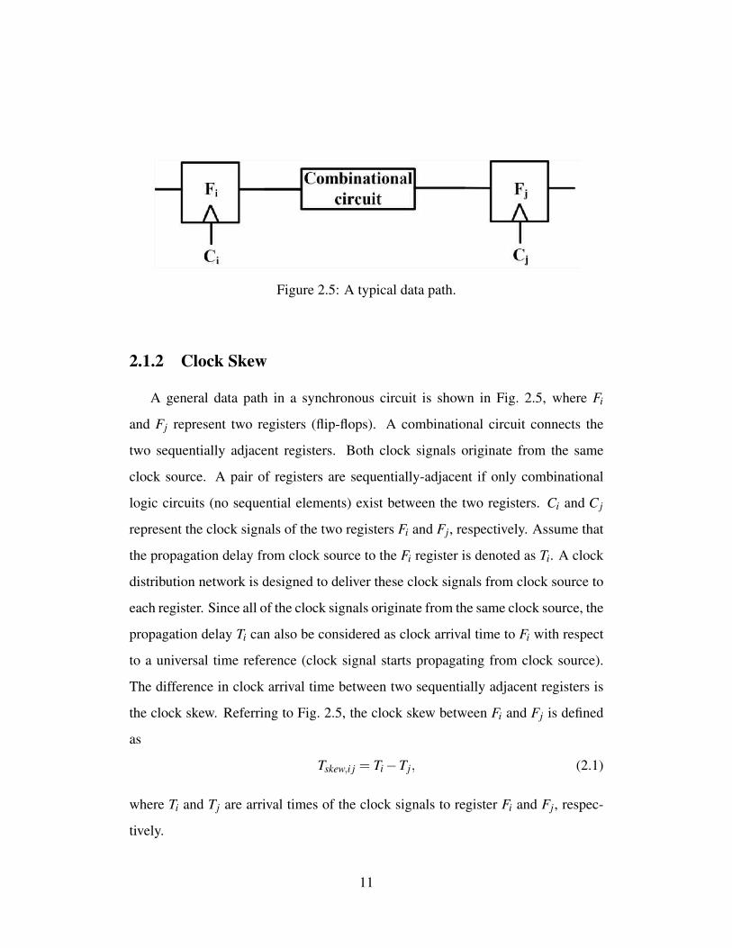
Figure 2.5: A typical data path.
2.1.2 Clock Skew
A general data path in a synchronous circuit is shown in Fig. 2.5, where Fi
and Fj represent two registers (flip-flops). A combinational circuit connects the
two sequentially adjacent registers. Both clock signals originate from the same
clock source. A pair of registers are sequentially-adjacent if only combinational
logic circuits (no sequential elements) exist between the two registers. Ci and C j
represent the clock signals of the two registers Fi and Fj, respectively. Assume that
the propagation delay from clock source to the Fi register is denoted as Ti. A clock
distribution network is designed to deliver these clock signals from clock source to
each register. Since all of the clock signals originate from the same clock source, the
propagation delay Ti can also be considered as clock arrival time to Fi with respect
to a universal time reference (clock signal starts propagating from clock source).
The difference in clock arrival time between two sequentially adjacent registers is
the clock skew. Referring to Fig. 2.5, the clock skew between Fi and Fj is defined
as
Tskew,i j = Ti−Tj, (2.1)
where Ti and Tj are arrival times of the clock signals to register Fi and Fj, respec-
tively.
11
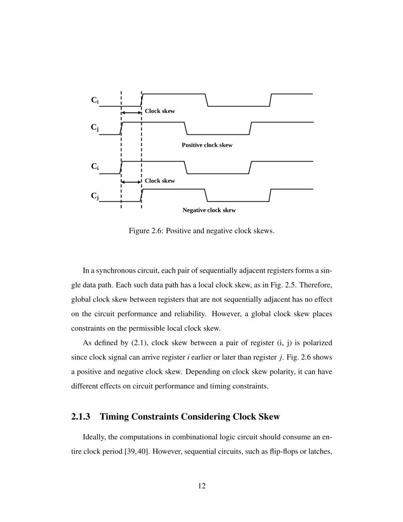
Ci
Cj
Ci
Cj
Clock skew
Clock skew
Positive clock skew
Negative clock skew
Figure 2.6: Positive and negative clock skews.
In a synchronous circuit, each pair of sequentially adjacent registers forms a sin-
gle data path. Each such data path has a local clock skew, as in Fig. 2.5. Therefore,
global clock skew between registers that are not sequentially adjacent has no effect
on the circuit performance and reliability. However, a global clock skew places
constraints on the permissible local clock skew.
As defined by (2.1), clock skew between a pair of register (i, j) is polarized
since clock signal can arrive register i earlier or later than register j. Fig. 2.6 shows
a positive and negative clock skew. Depending on clock skew polarity, it can have
different effects on circuit performance and timing constraints.
2.1.3 Timing Constraints Considering Clock Skew
Ideally, the computations in combinational logic circuit should consume an en-
tire clock period [39,40]. However, sequential circuits, such as flip-flops or latches,
12
cause overhead into this entire clock cycle. If the delay of the combinational logic
circuit is too large, the capture element will miss its setup time and may sample
the wrong data. This violation is called a setup time or max delay failure. This
violation can be fixed by reducing the delay of the logic or by increasing the clock
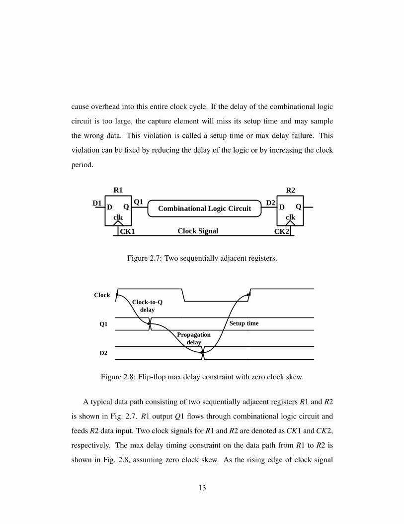
period.
QD
clk
Combinational Logic Circuit QD
clk
Clock Signal
Q1D1
CK1 CK2
R1 R2
D2
Figure 2.7: Two sequentially adjacent registers.
Clock
Q1
D2
Clock-to-Q
delay
Propagation
delay
Setup time
Figure 2.8: Flip-flop max delay constraint with zero clock skew.
A typical data path consisting of two sequentially adjacent registers R1 and R2
is shown in Fig. 2.7. R1 output Q1 flows through combinational logic circuit and
feeds R2 data input. Two clock signals for R1 and R2 are denoted as CK1 and CK2,
respectively. The max delay timing constraint on the data path from R1 to R2 is
shown in Fig. 2.8, assuming zero clock skew. As the rising edge of clock signal
13

CK1
Q1
D2
CK2
Clock-to-Q
delay
Propagation delay
Setup time
Clock skew
Figure 2.9: Flip-flop max delay constraint with positive clock skew.
CK1 triggers R1, the data at D1 is latched in. It should propagate to R1 output Q1
and through combinational logic circuit to D2, setting up at R2 before the next rising
edge of clock signal CK2. To satisfy max delay constraint, all of these events should
be completed within one clock period. Therefore, clock period should satisfy
Tclock ≥ tc2q + tcom + tsetup, (2.2)
where Tclock, tc2q, tcom and tsetup represent clock period, clock-to-Q delay, propaga-
tion delay of combinational logic circuit and setup time, respectively.
A max delay timing constraint with nonzero skew is depicted in Fig. 2.9. Clock
signal arrives R1 later than R2. Therefore, clock skew Tskew,12 is positive. In this
case, clock period should satisfy
Tclock ≥ Tskew,12 + tc2q + tcom + tsetup. (2.3)
According to (2.3), a positive clock skew reduces the effective clock period and
14

Clock
Q1
D2
Clock-to-Q
delay
Propagation
delayHold time
Figure 2.10: Flip-flop min delay constraint with zero clock skew.
increases the sequencing overhead. Alternatively, a negative clock skew provides
additional time for computations. Therefore, a negative clock skew can improve
max delay timing constraints.
Ideally, sequencing elements can be placed back-to-back without any combina-
tional logic. However, if the hold time is large and the clock-to-Q delay is small, the
capture element can incorrectly latch data on the same clock edge. This situation is
referred to as a race condition, hold time failure or min delay failure. This failure
can only be fixed by slowing down the data signal. Therefore, min delay violations
can only be fixed by redesigning the circuit.
A min delay timing constraint on the data path from R1 to R2 is shown in
Fig. 2.10, assuming zero clock skew. As the rising edge of clock signal CK1 trig-
gers R1, the data at D1 is latched in. It propagates through combinational logic
circuit and must not reach D2 until at least the hold time after the same clock edge,
15

CK1
Q1
D2
CK2
Clock-to-Q
delay
Propagation delay
Hold timeClock skew
Figure 2.11: Flip-flop min delay constraint with negative clock skew.
otherwise the early arrival of the data may corrupt the contents of R2. This implies
tc2q + tcom ≥ thold, (2.4)
where tc2q, tcom and thold represent clock-to-Q delay, propagation delay of combi-
national logic circuit and hold time, respectively.
A min delay timing constraint with nonzero skew case is shown in Fig. 2.11.
Clock signal arrives R1 earlier than R2. Therefore, skew is negative. To ensure the
correct functionality, the following inequality should be satisfied
Tskew,12 + tc2q + tcom ≥ thold. (2.5)
According to (2.5), a negative skew can offset the propagation delay of combina-
tional logic, making the circuit more sensitive to hold time violations. Alternatively,
a positive skew decreases the effective hold time, which lowers the chances of a hold
time failure.
16

2.1.4 Clock Tree Synthesis (CTS)
The process of a clock tree synthesis consists of two steps [41, 42]: first step is
to determine a set of clock arrival times for each register within the circuit, which
satisfies all of the synchronous timing constraints mentioned in Section 2.1.3. This
step is typically referred to as clock skew scheduling which is discussed in detail
in Chapter 5. The second step is the physical layout of the clock network that
implements the feasible clock schedule from step one, which is referred to as clock
routing.
A set of feasible clock arrival time for each register within the clock network
is generated after clock skew scheduling. The clock tree routing process constructs
a tree topology with minimum wiring cost, while implementing the specified skew
schedule generated in the previous step. Typically, a general clock routing algo-
rithm includes two steps. First step is to generate an abstract topology and second
step is to embed the abstract topology while satisfying the constraints. Various
clock routing algorithms were proposed in the literature, which can be categorized
into three domains: (1) zero-skew clock routing, (2) bounded skew routing, and
(3) useful-skew clock routing. In [43–45], the proposed algorithms are based on
zero-skew clock routing while minimizing wiring cost as an optimization objective.
The bounded skew routing algorithms were proposed in [46, 47], which are an ex-
tension of the common zero-skew: deferred merge embedding (DME) algorithm.
In [48, 48, 49], useful-skew based clock routing algorithms were developed while
minimizing the wire cost and overall clock buffer size. In Chapter 6, a slew-driven
clock tree synthesis methodology is proposed to simultaneously satisfy the clock
skew and slew while constructing the clock tree bottom-up. Contrary to the de-
lay/skew driven methodologies, the proposed approach prioritizes slew and reduces
17

S0
S1
S2 S3
v
u
Figure 2.12: An abstract tree.
the overall clock tree power.
An abstract topology G of a clock tree is a binary tree such that all of the sinks
are the leaf nodes of the binary tree. A nonleaf node is either the clock source or
internal nodes. Each internal node of G has two children, which are normally named
as “left child” and “right child”. The clock source node possibly has only one child.
The root of the abstract tree is denoted as s0, which is also the source driver. Each
non-root node v is connected to its parent, denoted as p(v), by an edge ev. The
clock signal from the source propagates through parent nodes to children nodes.
An abstract tree topology with three leaves s1, s2 and s3 is shown in Fig. 2.12.
The embedding of an abstract topology G to form an interconnect tree T in-
volves the mapping of each internal node v ∈ G to a location (xv, yv) in the floor-
plan, where xv and yv are the x and y coordinates, and replacing each edge e ∈G by
18

a rectilinear edge or path [41]. Note that most of the clock routing algorithms only
map the internal nodes in an abstract topology to physical locations on a floorplan
and do not actually route the interconnects, which can be accomplished by a router
tool. The wiring cost to route a tree T is the sum of all of its edges.
2.2 Existing Works on Low Voltage Clocking
Pangjun and Sapatnekar developed a low voltage/swing clock network by uti-
lizing level converters [24]. Both single voltage and dual voltage converters were
considered. A theoretical framework was proposed to appropriately position the
low-to-high level converters throughout the clock tree. For example, two sinks that
are physically close share a single converter to minimize the overall overhead. The
primary limitation of this approach is the conversion of the clock signal back to
full swing at the last stage of the clock tree. This practice significantly reduces the
power savings due to high switching capacitance at the sink nodes. In addition,
the slew constraint is considered as a secondary design objective after the merging
points are determined during clock tree synthesis. As observed in this research,
this approach generates a non-optimal low swing clock tree with reduced power
savings.
Asgari and Sachdev proposed a low swing clock network design methodology
using a single supply voltage [25]. In this approach, single voltage buffers are used
to adjust the clock swing throughout the clock network. Similar to [24], clock
voltage is restored to full swing at the last stage, thereby significantly reducing the
overall power savings. In addition, the clock swing is tuned by relying on the delay
of an inverter chain. Thus, the clock swing is highly dependent upon the output
19

load capacitance, limiting the proposed approach to only highly symmetric clock
networks such as H-trees.
More recently, low voltage clock networks have been investigated for near-
threshold systems that aim enhanced energy efficiency. In [28], Seok et al. investi-
gated the skew characteristics of various clock networks operating at low voltages.
The primary emphasis is on symmetric networks such as H-trees. Automated clock
tree synthesis algorithms were not considered. In [27, 29], Zhao et al. proposed a
deferred-merge embedding (DME) based clock tree synthesis method for low volt-
age clock networks with emphasis on clock slew. The proposed technique relies on
a computationally expensive procedure of storing multiple solutions in a bottom-up
fashion, followed by selecting an optimum solution for each node in a top-down
fashion. Clock frequencies of less than 10 MHz are considered, limiting the pro-
posed approach to only ultra low power systems where performance requirements
are low.
2.3 Primary Challenges in Developing a Low Voltage
Clock Network
Several challenges exist in the application of low voltage clocking to industrial
circuits with heavily gated clock networks. These challenges and proposed solu-
tions are summarized here.
20

2.3.1 Low Swing Operation at the Sinks: New Flip-Flop Cell
Traditional low swing clocking methodologies restore clock signals back to
full swing at the sinks since conventional flip-flops cannot be reliably used with
a low swing clock signal. A low swing clock signal either causes significant con-
tention/short circuit current (thereby significantly increasing the power consump-
tion) and/or increase clock-to-Q delay (thereby possibly violating the timing con-
straints) [50–52]. An important disadvantage of restoring back to full swing signal
is a significant reduction in power savings since the last stage of a clock network
consumes large power due to high capacitance. Thus, to maximize power savings,
a novel flip-flop cell is developed to enable low swing operation at the sinks while
still maintaining a full swing data signal, as further discussed in Chapter 3.
2.3.2 Satisfy Skew and Slew Constraints: Novel CTS and Level
Shifter
At scaled supply voltages (as required for low swing operation), clock inser-
tion delay increases, which in turn increases clock skew under variations. Fur-
thermore, the drive ability of the clock buffers is degraded, which significantly in-
creases clock slew. Satisfying the slew constraint at low swing operation therefore
becomes highly challenging [53, 54]. A larger number of clock buffers is typically
required which reduces the power savings. Research results demonstrate that an
optimum voltage swing level exists beyond which low swing clocking increases
overall power due to excessive buffering (assuming tight slew constraints) [55, 56].
A slew driven CTS algorithm is developed to satisfy the skew, slew constraints as
in full swing operation, while also reducing clock network power consumption, as
21

described in Chapter 6. A novel level-up shifter with dual supply voltage is also
proposed for selective low swing clocking, as described in Chapter 4. The pro-
posed level-up shifter enables a clock tree with both nominal and low voltages to
simultaneously satisfy performance requirements and reduce power consumption.
2.3.3 Degraded Enable Path Timing: Exploit Useful Skew
Figure 2.13: A simplified gated clock network consisting of five sinks, an integratedclock gating (ICG) cell, and an Enable path.
Practical clock networks are heavily clock gated to reduce the switching activity
factor of a clock signal, thereby reducing dynamic power. A common practice is to
use integrated clock gating (ICG) cells that consist of a sequential element to pre-
vent glitches in the gated clock signal, as shown in Fig. 2.13. An ICG cell has two
input pins (clock and Enable signals) and an output pin (gated clock signal). The
proposed low swing methodology should efficiently consider gated trees. Despite
full swing operation of the data signals, it has been observed that low swing gated
clock trees may violate timing constraints within an Enable path. Specifically, in
22

low swing operation, the delay between an ICG and flip-flops (gated by this ICG)
increases. Thus, the timing of the Enable path suffers due to skew between the
launching flip-flop and the capturing latch (within the ICG) [57,58]. Useful skew is
exploited for gated low swing clock trees to alleviate this issue, as further discussed
in Chapter 5.
23
Chapter 3
Flip-Flop Design to Facilitate Low
Swing Operation
Existing works on low swing/voltage clock networks are effective primarily for
low power applications that do not demand high performance. Achieving a reli-
able low swing clock network without sacrificing performance is challenging. The
interface between a low swing clock signal and flip-flop may increase clock-to-Q
delay, thereby reducing the timing slack within the data paths while also increasing
power consumption. To alleviate this issue, a common approach is to restore full
swing operation before the clock signal reaches flip-flops [24, 25]. This approach
significantly reduces power savings since the last stage of a clock network has high
switching capacitance. In this chapter, a novel D-type flip-flop design to facilitate
low swing operation is explored. The proposed DFF can work reliably with a low
swing clock signal while keeping the data signal as full swing, i.e., not sacrificing
the circuit performance. The rest of this chapter is organized as follows. Effect
24
of low swing operation on flip-flop is investigated in Section 3.1. Existing works
on low swing flip-flops are discussed in Section 3.2. The proposed topology is de-
scribed in Section 3.3. Simulation results in 45 nm and 32 nm technology nodes are
provided in Section 3.4. Finally, the proposed design is summarized in Section 3.5.
3.1 Effect of Low Swing Operation on Flip-Flop
As emphasized in Section 2.2, it is critical to have low swing operation at the
DFF clock pins to maximize power savings. A conventional DFF cell designed
for full swing operation, however, cannot be used when the clock voltage swing is
reduced due to degradations in reliability and power consumption, as described in
the following subsections.
3.1.1 Reliability
In a typical DFF cell, clock signals drive both NMOS and PMOS transistors
(as in transmission gated based and tri-state inverter based DFFs). If the same DFF
topology is used with a low swing clock signal (whereas the data signal is still at full
swing to maintain performance), the PMOS transistors driven by the clock signal
fail to completely turn off when the clock signal is high. For example, consider
a 45 nm technology with a nominal VDD of 1 V. If the clock swing is reduced to
0.7×VDD, the gate-to-source voltage of the PMOS transistors becomes -0.3 V since
the data signal is at full swing and the inverters within the flip-flop are connected
to nominal (full swing) VDD. Since -0.3 V is sufficiently close to the threshold
voltage of PMOS transistors in this technology, this behavior significantly affects
the operation reliability of a traditional DFF cell driven by a low swing clock signal.
25

1
D Q
CLK_in CLK_b CLK
CLK
CLK_b
CLK_b
CLK
CLK
CLK_b CLK_b
CLK
Low VDD Low VDD
High VDD
High VDD
High VDD
High VDD
High VDD High VDD
Clock sub-circuit
Figure 3.1: A typical transmission gate based D flip-flop topology driven by a lowswing clock signal.
As an example, consider a rising-edge triggered master-slave flip-flop. When the
clock signal is high, the master latch should be turned off. However, due to low
swing clock signal, the transmission gate (or tri-state inverter) within the master
latch cannot completely turn off. If the data signal is in a different state than the
stored data within the master latch, a race condition occurs which can possibly
produce a metastable state.
To better illustrate the unreliability of conventional DFF cells operating with a
low swing clock signal, a traditional transmission gate based D flip-flop, as shown in
Fig. 3.1, is simulated with a 45 nm technology node when the clock swing is 0.7 V.
Note that the clock signal and inverted clock signal are internally generated by using
two inverters. This circuit is referred to as the clock sub-circuit, as also depicted
in Fig. 3.1. Note that the inverters within the clock sub-circuit are connected to a
low supply voltage to provide low swing clock signals. Since the PMOS transistors
driven by the clock signals are not completely turned off, internal nodes experience
26
a glitch as high as 400 mV. Furthermore, in the slow corner, the DFF cell fails to
correctly latch the data signal. Thus, a new topology is required that can reliably
operate with a low swing clock signal and a full swing data signal.
Note that an alternative solution is to integrate a level shifter within the DFF
cell to restore a full swing clock signal [59]. Thus, the clock signal is restored to
full swing operation before reaching PMOS transistors. This approach is similar
to existing level shifting DFF cells for dual voltage systems [60], but the level of
the clock signal is shifted rather than the data signal. This approach, however,
significantly increases the overall power consumption of the DFF cell due to the
integrated level shifter. Thus, the power saved at the last stage of the clock network
is lost within the DFFs, making this approach impractical for the primary objective
of this work.
3.1.2 Power Consumption
The reliability issue described in the previous subsection can be fixed by con-
necting the inverters within the clock sub-circuit of a conventional DFF to the nom-
inal VDD, producing a single voltage flip-flop driven by a low swing clock signal. In
this case, these inverters also function as single voltage, low-to-high level shifters
and the transmission gates receive full swing clock signals. The primary limitation
of this approach is an unavoidable increase in power consumption due to significant
static current drawn by the inverters within the clock sub-circuit. To better illustrate
this behavior, a conventional DFF is simulated when a low swing clock signal is
applied to the clock pin while the clock sub-circuit is connected to a nominal VDD.
The overall power consumption is shown in Fig. 3.2 as a function of clock swing for
both 45 nm and 32 nm technologies. As shown in this figure, DFF power increases
27

0.5 0.6 0.7 0.8 0.9 19
9.5
10
10.5
11
11.5
12
12.5
13
13.5
14
Clock voltage swing ( VDD
)
DF
F p
ower
dis
sipa
tion
( W
)
0.5 0.6 0.7 0.8 0.9 13
3.1
3.2
3.3
3.4
3.5
3.6
3.7
3.8
Clock voltage swing ( VDD
)D
FF
pow
er d
issi
patio
n ( W
)
45 nm technology 32 nm technology
Figure 3.2: Increase in power consumption when a conventional DFF is driven witha low swing clock signal while the clock sub-circuit is connected to a nominal VDD.
by approximately 48% and 23% when the clock swing is reduced to 0.6×VDD in,
respectively, 45 nm and 32 nm technologies.
Thus, a conventional flip-flop designed for a full swing clock signal suffers from
a prohibiting trade-off between reliability and power consumption. The reliability
issue may cause the flip-flop to latch a wrong data due to large spikes, which is
exacerbated in corner cases. Alternatively, the increase in power consumption is
not tolerable since it conflicts with the primary purpose of this work.
3.2 Existing Low Swing Flip-Flops
Existing flip-flop topologies developed to operate with a low swing clock signal
are summarized in this action. The strengths and weaknesses of each topology are
discussed.
28

QN Q
D
CLK
CLK
_CLK
_CLK
CLOCK
CLOCK
CLK
_CLK
N1
N2
N3
N4
N6
N7
N5
P1
P2
P3
P4
(a)
Vwell
CLK
CLK
CLK
D
Q QN
N1
N2
N5
N3
N4
N6
P1P2
P4P3
(b)
VDD_L
QN
N1
N2
N3
N6
N7
N8
N4N5
P1P2
P3
Q
(c)
D
VDD_L
_DD
DD
DD
_DD
CLK
Q
_Q
N1
N2
N3
N4
P1
P2
P3
P4
P5
P6
(d)
Figu
re3.
3:E
xist
ing
low
swin
gfli
p-flo
pto
polo
gies
(a)C
2 MO
San
dse
nse
ampl
ifier
base
dlo
wsw
ing
flip-
flop,
L-C
2 MO
S-SA
[1],
(b)r
educ
edcl
ock
swin
gfli
p-flo
p,R
CSF
F[2
],(c
)NA
ND
-typ
eke
eper
flip-
flop,
ND
KFF
[3],
and
(d)c
onte
ntio
nre
duce
dfli
p-flo
p,C
RFF
[4].
29

A flip-flop topology for a low swing clock signal based on clocked CMOS
method (C2MOS) and sense amplifier (SA) has been proposed in [1], as illus-
trated in Fig. 3.3(a). This circuit, referred to as L-C2MOS-SA, reduces the charge-
discharge capacitance and implements the conditional pre-charge and discharge
technique to achieve low power consumption. The circuit is area efficient and a
considerable reduction in leakage current is also obtained with this topology. The
original version of this topology utilizes diode-connected PMOS transistors within
the clock sub-circuit to reduce voltage swing, as depicted in Fig. 3.3(a). Diode-
connected PMOS transistors, however, significantly degrade clock slew due to re-
duced supply voltage in stacked PMOS transistors, making this topology imprac-
tical for industrial circuits. This issue is exacerbated in the slow corner operation.
Thus, to achieve a fair comparison, this topology is modified in this work where
the clock sub-circuit has a second power supply voltage for low swing rather than
having diode-connected PMOS transistors. This modified version is referred to as
L-C2MOS-SA-2. Also note that this topology requires a full swing clock signal
at the slave stage, which defies our primary objective of having only a low swing
clock signal throughout the entire clock network.
Another flip-flop topology has been proposed in [2] for low swing operation.
This topology, referred to as reduced clock swing flipflop (RCSFF), is depicted in
Fig. 3.3(b). As shown in this figure, this design utilizes an additional low supply
voltage within the clock sub-circuit to provide low swing clock signal, similar to
the proposed topology in this research. However, in [2], the low swing clock signal
is used to drive PMOS transistors that are connected to a higher (full) supply volt-
age. As mentioned earlier, these transistors cannot completely turn off, producing
functionality and reliability issues in addition to significantly increasing both short
30

circuit and leakage current. To alleviate this issue, authors have utilized the well
known bulk biasing technique. Specifically, the bulk nodes are connected to a sep-
arate well biased at a greater voltage, thereby increasing the threshold voltage of
these PMOS transistors. An additional well, however, not only increases the phys-
ical area and complexity of the design, but also requires a triple-well process that
is not common in standard digital CMOS technologies. Furthermore, at the corner
cases, this issue is exacerbated despite the use of well biasing.
The NAND-type keeper flip-flop topology proposed in [3], referred to as ND-
KFF, is illustrated in Fig. 3.3(c). As opposed to the previous topology, this circuit
does not require a separate well at the expense of excessive leakage current that
flows through the transistors P2, N1-N3 when node X is at logic low. Furthermore,
a contention occurs at node X since the level-keeping transistors, i.e., P2, N4, N5
and I1-I2 have a race condition when node X transitions from logic low to logic
high, thereby increasing the transition time and clock-to-Q delay of the output.
This issue is exacerbated during the worst-case delay analysis of the circuit, which
can be partially controlled by carefully sizing the transistors.
In [4], authors have proposed a contention reduced flip-flop referred to as CRFF
and is depicted in Fig. 3.3(d). This circuit utilizes a pulsed clock signal to pro-
vide a short transparency window during which the output is discharged through
the NMOS transistors N1-N4. During this transparency window, the clocked tran-
sistors P5 and P6 disconnect the latch (I1-I2), thereby reducing contention current.
Transistors P1 and P2 are controlled by input D through P3 and P4 which further
reduces the contention current. However, low swing clock signal is used to drive
PMOS transistors P5 and P6, thereby suffering from the aforementioned issues of
functionality and reliability.
31

3.3 Proposed D-Flip-Flop Topology for Low Swing
Clocking
The proposed DFF topology, depicted in Fig. 3.4(a), is based on the most com-
monly used, static D flip-flop shown in Fig. 3.1. Rather than using transmission
gates, however, pass gates with NMOS transistors (N1, N2, N5, and N6) are utilized
as the switches in both master and slave latches. Thus, when the low swing clock
signal is at logic high, N1 and N6 can completely turn off. Pass gates, however,
cannot transfer a full voltage to the output. This issue is critical since the incoming
data signal operates at full swing. Thus, node A cannot reach a full VDD, thereby in-
creasing the short-circuit and leakage current in the following stages in addition to
increasing the clock-to-Q delay. Furthermore, pass transistors are known to be less
robust to process variations. To alleviate these issues, a pull-up network consisting
of two PMOS transistors is added to both master and slave latches (P1 to P4). When
the master node M transitions to logic low, P1 turns on. If the data signal is also at
logic low, then node A is pulled to full VDD through P1 and P2. Note that P2 (in
the master latch) and P4 (in the slave latch) are added to prevent contention current
(and therefore reduce power consumption) when the data signal is at logic high and
clock signal is at logic low. In this situation, N1 is on and node A is discharged
through N1 and the inverter. If P2 does not exist, a race condition occurs at node
A since N1 should be stronger than P1, which pulls node Y to full VDD. Finally,
a pull-down logic is added to both master and slave latches to enhance clock-to-Q
delay (N3, N4, N7, and N8). Specifically, when data and clock signals are at logic
low, the pull-down logic is active and pulls the master node M to ground, triggering
P1. Thus, node A quickly reaches full VDD. Note that the master node does not need
32

(a)
(b)
Figure 3.4: Proposed DFF topology that can reliably work with a low swing clocksignal whereas the data and output signals are at full swing, (a) schematic, (b) layoutin the 45 nm technology.
to wait for node A to rise through a weak pass transistor and activate the inverter.
Instead, the pull-down logic completes this transition relatively faster. Also note
33

that the clock sub-circuit is identical to the sub-circuit shown in Fig. 3.1. Layout of
the proposed DFF topology in a 45 nm technology is depicted in Fig. 3.4(b).
3.4 Simulation Results
The proposed low swing flip-flop is compared with the conventional full swing
flip-flop on power and clock-to-Q delay as clock swing varies in Section 3.4.1. A
comparative analysis with existing works including robustness of each topology to
PVT variations is presented in Section 3.4.2.
3.4.1 Comparison with Conventional Full Swing Flip-flop
0 0.5 1 1.5
0
0.2
0.4
0.6
0.8
1
Time (ns)(a)
Vol
tage
(v)
dataclockQ
0 0.5 1 1.5
0
0.2
0.4
0.6
0.8
1
Time (ns)(b)
Vol
tage
(v)
dataclockQ
Figure 3.5: Correct functionality of the proposed low swing DFF cell in 32 nmtechnology: (a) latching logic-low, (b) latching logic-high.
The proposed low swing DFF topology is designed in both 45 nm and 32 nm
technologies. To illustrate proper functionality, full swing data, low swing clock,
and full swing output (Q) signals are plotted in Fig. 3.5 for the 32 nm technology
34

while driving a 5 fF load capacitance. As shown in this figure, the DFF cell can
successfully latch both logic-low and logic-high full swing data signals after the
rising edge of the low swing clock signal. Note that the output reaches nominal
(full swing) VDD and the DFF cell does not exhibit glitches in any of the internal
nodes.
0.5 0.6 0.7 0.8 0.9 16
7
8
9
10
11
12
13
14
Clock voltage swing ( VDD
)
(a)
DF
F p
ower
dis
sipa
tion
( W
)
FSDFF
LSDFF
0.5 0.6 0.7 0.8 0.9 12.5
3
3.5
4
4.5
5
Clock voltage swing ( VDD
)
(b)
DF
F p
ower
dis
sipa
tion
( W
)
FSDFF
LSDFF
Figure 3.6: Power consumption comparison of the proposed low swing DFF cell(LSDFF) with the conventional full swing DFF cell (FSDFF): (a) 45 nm technology,(b) 32 nm technology.
To compare the proposed low swing DFF cell (LSDFF) with the conventional
full swing DFF cell (FSDFF), power and clock-to-Q delay are analyzed as a func-
tion of clock swing for both 45 nm and 32 nm technologies. The overall power
consumption is compared in Fig. 3.6. According to this figure, for both technolo-
gies, FSDFF consumes less power than LSDFF at relatively large clock swings. As
the clock swing is reduced, however, LSDFF significantly outperforms FSDFF. The
crossover voltage is approximately 0.85 V for 45 nm technology and 0.81 V for 32
35

nm technology. At a clock swing of 0.6 V, LSDFF consumes approximately 53%
and 30% less power than FSDFF in, respectively, 45 nm and 32 nm technologies.
0.5 0.6 0.7 0.8 0.9 160
65
70
75
80
85
90
Clock voltage swing ( VDD
)
(a)
DF
F c
lock−
to−
Q d
elay
(ps
)
FSDFF
LSDFF
0.5 0.6 0.7 0.8 0.9 160
65
70
75
80
85
90
95
100
105
Clock voltage swing ( VDD
)
(b)
DF
F c
lock−
to−
Q d
elay
(ps
)
FSDFF
LSDFF
Figure 3.7: Clock-to-Q delay comparison of the proposed low swing DFF cell (LS-DFF) with the conventional full swing DFF cell (FSDFF): (a) 45 nm technology,(b) 32 nm technology.
The clock-to-Q delay of the LSDFF and FSDFF is compared as a function of
clock swing in Fig. 3.7. According to this figure, for both technologies, LSDFF
outperforms FSDFF in all clock swings except 0.6 V in 32 nm technology. The
clock-to-Q delay of the LSDFF at this point is only 5 ps more than FSDFF. It is im-
portant to note that the LSDFF running at 0.65 V can achieve less or equal clock-to-
Q delay than FSDFF running at full swing. This characteristic is highly important
to maintain data path timing the same (or with more slack) when the conventional
flip-flops are replaced with LSDFFs. The clock-to-Q delay in LSDFF is adjusted
by sizing the last two inverter stages. Note that the clock pin capacitance remains
the same as FSDFF, since the size of the first inverter within the clock subcircuit
(see Fig. 3.1) is kept constant. Also note that, for a fair analysis, the size of the
36

transistors within the flip-flops remains the same at each clock voltage.
The timing constraint characterization of the LSDFF and FSDFF demonstrates
that the proposed topology has comparable setup and hold times, as listed in Ta-
ble 3.1. In particular, for hold time, LSDFF slightly outperforms FSDFF. This
characteristic is important to ensure that no min-delay constraint violations are in-
troduced in short data paths. Alternatively, for setup time, FSDFF slightly outper-
forms LSDFF. The difference, however, is sufficiently small as compared with the
clock period in multigigahertz designs.
Topology45 nm 32 nm
FSDFF LSDFF FSDFF LSDFF
Setup time (ps)Latch 1 11 23 4 18Latch 0 12 28 6 26
Hold time (ps)Latch 1 -1 -15 -2 -15Latch 0 -7 -19 2 -7
Table 3.1: Setup and hold time simulation results of full swing DFF and the pro-posed low swing DFF at 45 and 32 nm technology nodes.
The proposed LSDFF has also been simulated at the slow and fast corners to
evaluate the robustness of the topology to PVT variations. As listed in Table 3.2,
at a clock swing of 0.7 V, the proposed topology achieves reliable operation and
outperforms the conventional topology at each corner (nominal, slow, and fast).
Finally, the cell area consumed by the proposed and existing topologies is listed
in Table 3.3. According to Table 3.3, LSDFF consumes 50% and 55% additional
area for, respectively, 45- and 32-nm technologies. The effect of this increase in
the overall die area, however, is expected to be below 10% considering the typical
percentage of the flip-flops in a design.
37

Topology45 nm 32 nm
FSDFF LSDFF FSDFF LSDFFNominal corner (TT model, 1.0V and 1.05V supply and 25C)Clock-to-Q delay (ps) 86.16 68.39 95.93 77.50Dynamic power (µW) 10.75 7.24 3.63 2.77Worst corner (SS model, 0.9V and 0.95V supply and 125C)
Clock-to-Q delay (ps) 183.95 180.44 181.86 175.19Dynamic power (µW) 6.83 5.86 2.18 2.05
Best corner (FF model, 1.1V and 1.15V supply and -40C)Clock-to-Q delay (ps) 57.02 26.12 55.06 15.69Dynamic power (µW) 21.62 9.28 9.69 9.78
Table 3.2: Corner simulation results of full swing DFF and the proposed low swingDFF at 45 and 32 nm technology nodes.
Topology Area (µm×µm)
45 nmFSDFF 3.285×2.67=8.77LSDFF 4.93×2.67=13.16
32 nmFSDFF 2.674×1.672=4.47LSDFF 4.166×1.672=6.96
Table 3.3: Layout areas of full swing DFF and the proposed low swing DFF at 45and 32 nm technology nodes.
3.4.2 Comparison with Existing Low Swing Flip-flops
The proposed flip-flop topology and the previous circuits in existing work (L-
C2MOS-SA [1], L-C2MOS-SA-2 [1], RCSFF [2], NDKFF [3], and CRFF [4]) are
designed using a 45 nm technology with a nominal supply voltage of 1 V and all of
the simulations are performed using Spectre [61]. The clock signal has a reduced
swing of 0.7 V. The clock and data frequencies are, respectively, 1.5 GHz and 150
MHz. Each flip-flop drives an output load capacitance of 5 fF. To achieve a fair
comparison, all of the flip-flops are sized to produce approximately equal clock-
38

to-Q delay. The simulations results including a comparative analysis with existing
work are presented in Section 3.4.2.1. Robustness of each topology to process,
voltage, and temperature variations is investigated in Section 3.4.2.2.
3.4.2.1 Comparative Analysis
The simulation results are listed in Table 3.4, comparing clock-to-Q delay, power
consumption, power-delay product (PDP), leakage power, overall transistor size,
and setup and hold times of all of the flip-flops. Note that the leakage power listed
in this table is obtained by averaging the leakage power obtained from four possible
static combinations of the data and clock signals.
As listed in Table 3.4, the proposed topology achieves, on average, 38.1% and
44.4% reduction in, respectively, dynamic power and power-delay product while
exhibiting similar clock-to-Q delay. L-C2MOS-SA [1] achieves the least leakage
power that is approximately 45% less than the proposed topology. L-C2MOS-
SA [1], however, exhibits degraded behavior at the worst-case corners, as described
in Section 3.4.2.2. The proposed topology exhibits the second lowest leakage
power, achieving significant reduction, particularly as compared to NDKFF [3] and
CRFF [4]. Overall transistor width of the proposed topology is less than the other
topologies except L-C2MOS-SA [1]. The setup-hold time characterization of each
topology is also performed, as listed in the last two columns [62]. Similar to some
other topologies, the proposed flip-flop exhibits a negative setup time.
The effect of clock swing voltage level on clock-to-Q delay and power con-
sumption is also investigated for each flip-flop, as depicted in Fig. 3.8.
According to Fig. 3.8(a), clock-to-Q delay increases as the clock swing is re-
duced in each topology. For L-C2MOS-SA [1], NDKFF [3], and CRFF [4], clock
39

Tabl
e3.
4:C
ompa
riso
nof
the
prop
osed
topo
logy
with
exis
ting
wor
kun
der
nom
inal
oper
atin
gco
nditi
ons
with
acl
ock
volta
gesw
ing
of0.
7×V D
D.E
ach
topo
logy
issi
zed
toac
hiev
eap
prox
imat
ely
equa
lclo
ck-t
o-Q
dela
y.
Flip
-flop
Clo
ck-t
o-Q
Ove
rall
PDP
Lea
kage
Ove
rall
tran
sist
orSe
tup
Hol
d
topo
logy
dela
ypo
wer
(fW
.s)
pow
erw
idth
time
time
(ps)
(µW
)(n
W)
NM
OS
PMO
S(p
s)(p
s)
(nm
)(n
m)
L-C
2 MO
S-SA
[1]
69.7
8.0
0.56
37.2
2395
2950
27.9
0.9
L-C
2 MO
S-SA
-2[1
]71
.39.
30.
6734
.541
9535
5017
.5-9
.2
RC
SFF
[2]
70.6
17.2
1.22
82.0
6840
5500
-26.
942
.6
ND
KFF
[3]
69.4
12.0
0.83
196.
650
5039
00-6
.0-6
2.7
CR
FF[4
]70
.310
.50.
7420
1.5
4650
5300
-20.
292
.9
Prop
osed
LSD
FF64
.16.
60.
4268
.126
5034
50-1
.717
.8
40

0.35 0.4 0.45 0.5 0.55 0.6 0.65 0.7 0.75 0.850
100
150
200
250
300
Clock voltage swing (V)
Clo
ck−
to−
Q d
elay
(ps
)
PROPOSED
L−C2MOS−SA−2RCSFFNDKFFCRFF
(a)
0.35 0.4 0.45 0.5 0.55 0.6 0.65 0.7 0.75 0.86
8
10
12
14
16
18
20
Clock voltage swing (V)
Pow
er d
issi
patio
n (
W)
PROPOSED
L−C2MOS−SA−2RCSFFNDKFFCRFF
(b)
Figure 3.8: Effect of clock swing voltage level on clock-to-Q delay and powerconsumption for each flip-flop topology: (a) Clock-to-Q delay vs. clock voltageswing, (b) power consumption vs. clock voltage swing.
swing cannot be reduced below 0.6 V since these circuits fail to latch the input data
at clock swings lower than 0.6 V. Note that the clock-to-Q delay is highly sensi-
tive to voltage swing for NDKFF [3]. The proposed topology can reliably latch
the input data for a clock swing as low as 0.5 V (half VDD). Furthermore, the pro-
posed topology exhibits relatively low sensitivity to voltage swing. RCSFF [2] is
the only topology that can work with a clock swing as low as 0.4 V. However, the
clock-to-Q delay significantly increases below 0.5 V, making this operating point
impractical. Furthermore, RCSFF [2] consumes significantly more power than the
proposed topology, as listed in Table 3.4.
The dependence of power consumption on clock voltage swing is shown in
Fig. 3.8(b). According to this figure, the proposed topology exhibits the lowest
power consumption at each clock swing voltage. Note that from 0.7 V to 0.6 V,
the overall power is slightly reduced whereas from 0.6 V to 0.5 V, there is a slight
increase. The overall effect of clock swing on power depends upon two factors: 1)
41

Flip-flop topologyCLK-to-Q delay
(ps) atSS-0.9V-165C
Overalltransient power(µW) at FF-1.1V
Leakage power(µW) at
FF-1.1V-165C
L-C2MOS-SA [1] Failure 10.8 (T=165C) 0.6
L-C2MOS-SA-2 [1] 178.8 11.3 (T=165C) 0.6
RCSFF [2] Failure 21.5 (T=-40C) 1.5
NDKFF [3] 210.0 17.2 (T=165C) 2.5
CRFF [4] 175.7 17.7 (T=165C) 3.8
This work 150.8 8.9 (T=-40C) 1.1
Table 3.5: Comparison of the proposed topology with existing work under worst-case operating conditions for clock-to-Q delay, overall transient power, and leakagepower. FF and SS correspond, respectively, to fast and slow models for both NMOSand PMOS transistors.
partial reduction in power since the clock sub-circuit consumes less power with a
lower swing, 2) partial increase in power due to a greater contention current with
a lower clock swing. If the first factor outweighs the second factor, overall power
is reduced as the clock swing is reduced. Note that CRFF [4] is the only topol-
ogy where power consumption significantly increases with a lower clock swing,
indicating the dominance of the second factor.
3.4.2.2 Robustness to Variations
A critical challenge in nanoscale ICs is the variations incurred during fabrica-
tion and fluctuations in operating voltage and temperature. The behavior of a circuit
to these variations is important to evaluate the overall robustness. To investigate
this issue, each flip-flop topology is simulated in the worst-case corner for delay,
transient power, and leakage power. The results are listed in Table 3.5. Note that
42
L-C2MOS-SA [1] and RCSFF [2] fail to latch the input data at the worst-case cor-
ner for delay, determined by the slow process models for both NMOS and PMOS
transistors, 0.9 V VDD (90% of the nominal VDD) and 165C temperature.
The proposed topology exhibits the lowest clock-to-Q delay (approximately
20% lower, on average) in the worst-case corner even though each topology ex-
hibits similar delays in the nominal case (see Table 3.4). This trend demonstrates
that the clock-to-Q delay of the proposed topology exhibits the least sensitivity to
process and environmental variations.
Similar to the nominal case, the proposed topology consumes the least transient
power in the worst-case, as determined by the fast process models for both NMOS
and PMOS transistors and 1.1 V VDD (110% of the nominal VDD). Note that the
temperature that corresponds to the worst-case corner for overall power depends
upon the topology due to inverted temperature dependence [63].
Specifically, in RCSFF [2] and the proposed topologies, the worst-case transient
power occurs at the lowest temperature whereas the other topologies consume the
largest power at the highest temperature. Note that inverted temperature depen-
dence also applies to the worst-case delay analysis and therefore each topology is
simulated with both the lowest and highest temperatures. However, largest clock-
to-Q delay occurs at the highest temperature in each topology, as shown by the
second column in Table 3.4. Finally, the worst-case leakage power, determined by
the fast process models, 1.1 V VDD, and highest temperature, is provided in the last
column. The trend is similar to the nominal results where the proposed topology
consumes the second least leakage power, after L-C2MOS-SA [1].
The variation analysis provided in this section demonstrates that the proposed
topology can reliably operate at the worst-case delay and power corners, unlike
43

some of the existing topologies that fail at the worst-case delay corner. Further-
more, the proposed topology consumes the least worst-case power consumption
and exhibits the least sensitivity to worst-case delay corner.
3.5 Summary
In this chapter, a D-type static flip-flop is proposed to facilitate low swing op-
eration. It can reliably operate with a low swing clock signal, thereby enabling low
swing operation throughout the entire clock network. Thus, power savings are max-
imized. Simulation results on power-delay product, corner performance, setup/hold
time demonstrate the superiority of the proposed DFF at each clock swing for both
45 nm and 32 nm technologies.
44

Chapter 4
Level Shifter for Selective Low Swing
Clocking
In clock trees with highly aggressive design constraints (such as small skew and
slew), it may not be practical to lower the clock voltage of the entire clock tree.
Selective low voltage clocking has been considered for such situations where part
of the clock tree operates at a reduced voltage (to save power) and the rest of the
tree operates at nominal voltage to satisfy the performance constraints. Thus, a low
overhead level shifter is required to restore clock voltage level. In Fig. 4.1, sink
2 and 3 are restored to full swing operation through a level-up shifter to satisfy
their timing constraint, while the rest of the sinks are still in low swing operation to
achieve power savings.
Existing level shifters can be categorized under two primary classes: 1) shifters
based on conventional, cross-coupled topology with differential output [64–67], 2)
shifters based on bootstrapping [68, 69]. Shifters in the first group enhance the
45

Figure 4.1: Selective low swing clocking.
delay of the level shifting by exploiting cross-coupled PMOS transistors whereas
shifters in the second group enhance the power consumption by reducing the swing
at the internal voltage nodes. In some applications where sub-threshold circuits are
interfaced with super-threshold operation, wide range level shifters are required, as
proposed in [65, 70, 71]. Level shifters with a single supply voltage have also been
proposed [72, 73]. However, shifting voltage swing with a single supply voltage
typically produces large leakage current and long signal transition times.
A conventional buffer consisting of two inverters powered by the lower supply
voltage VddL can reliably function as a level-down shifter since there is no short
circuit or leakage issue [24]. A conventional buffer, however, cannot reliably func-
tion as a level-up shifter since the incoming signal with a lower supply voltage
drives inverters powered with a higher supply voltage. This situation causes unrea-
sonably high short circuit and leakage current that is not tolerable in most of the
46

applications. For example, in 45 nm technology, if a conventional buffer is used as
a level-up shifter, short circuit current is approximately 31% of the overall power
consumption while leakage current is in the range of microamps.
In this chapter, a level-up shifter with dual supply voltage is proposed to enable
selective low swing clocking. It reduces the transient power of conventional cross-
coupled topology while consuming significantly less area as compared to bootstrap-
ping technique. A relatively fast response is also achieved. The rest of this chapter
is organized as follows. The traditional cross-coupled level shifter and bootstrap-
ping techniques are summarized in Section 4.1 and Section 4.2, respectively. The
proposed level shifter is described in Section 4.3. Simulation results and related
discussion are presented in Section 4.4. Finally, the chapter is concluded in Sec-
tion 4.5.
4.1 Cross-Coupled Topology
Conventional level shifter using cross-coupled PMOS transistors is depicted in
Fig. 4.2(a). As shown in this figure, the incoming low voltage signal is inverted
using an inverter connected to a low voltage domain, VddL. Cross-coupled PMOS
transistors P1 and P2 are used to pull output to the high voltage, VddH . Leakage
issue of the conventional buffer is alleviated since P1 and P2 are not driven by
the incoming signal. However, this topology exhibits relatively high short circuit
current during transition (either through P1 and N1 or through P2 and N2) even
when the input transitions are fast.
47

(a)
(b)
Figure 4.2: Primary existing level shifters: (a) conventional cross-coupled topology,(b) bootstrapping technique.
4.2 Bootstrapping Technique
Bootstrapping technique, as depicted in Fig. 4.2(b), has been proposed to re-
duce the transient power during level shifting. Voltage swing at specific nodes is re-
duced, thereby saving power, particularly when driving large capacitive loads [69].
In Fig. 4.2(b), two boot capacitors Cboot1 and Cboot2 replace NMOS transistors to
maintain the voltage difference at the gate terminals of P2 and N2. Thus, the pull-
48

down NMOS N2 at output stage is driven between 0 and VddL whereas the pull-up
PMOS is driven between VddH −VddL and VddH . Bootstrapping technique achieves
lower power at the expense of significant increase in physical area due to the rela-
tively large boot capacitors, determined by
Cboot1 =CA ·2 ·Vdiode
VddL−2 ·Vdiode, (4.1)
where CA is total capacitance at node A to ground, excluding Cboot1. Vdiode is the
voltage drop across a single diode, similar to D0 in [68]. When VddL is sufficiently
close to 2 ·Vdiode, boot capacitor becomes considerably large. In [69], cross-coupled
load is divided into half and only one boot capacitor is required, partially reducing
the overall area requirement.
4.3 Proposed Level Shifter for Selective Low Swing
Clocking
The proposed level-up shifter schematic and physical layout are illustrated in
Fig. 4.3(a) and Fig. 4.3(b). The proposed design is based on a traditional buffer
with certain modifications to minimize short-circuit current, reduce delay while
minimizing the overall number of transistors. Since an input signal at the VddL
level cannot completely turn off PMOS transistors, an inverter is designed with two
NMOS transistors (N1 and N2) where N2 is driven by inverted input signal. When
input signal is at logic low, N1 is off and N2 is on. Node A is at VddH−Vth since N2
cannot pass a full VDD. To compensate for the threshold voltage drop, two keeper
PMOS transistors, P1 and P2, are added. When output node goes low, P2 is on.
49

(a)
(b)
Figure 4.3: Proposed level shifter (a) schematic, (b) physical layout.
Since input signal is also at logic low, node A is pulled to VDDH. Note that P1 is
added to prevent short-circuit current when node A is being discharged through N1.
A pull down NMOS transistor, N5, is added to reduce the delay when the output
is having a high-to-low transition. If the input signal is at logic high, N1 is on, N2
is off. Node A is discharged through N1. Since P1 is off, no short-circuit current
exists. As node A is discharged, output rises to VDDH through P4. The input and
50
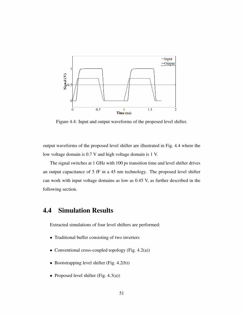
Figure 4.4: Input and output waveforms of the proposed level shifter.
output waveforms of the proposed level shifter are illustrated in Fig. 4.4 where the
low voltage domain is 0.7 V and high voltage domain is 1 V.
The signal switches at 1 GHz with 100 ps transition time and level shifter drives
an output capacitance of 5 fF in a 45 nm technology. The proposed level shifter
can work with input voltage domains as low as 0.45 V, as further described in the
following section.
4.4 Simulation Results
Extracted simulations of four level shifters are performed:
• Traditional buffer consisting of two inverters
• Conventional cross-coupled topology (Fig. 4.2(a))
• Bootstrapping level shifter (Fig. 4.2(b))
• Proposed level shifter (Fig. 4.3(a))
51

Note that each level shifter is designed and extracted using a 45 nm technology.
Extracted simulations are achieved at 1 GHz with 100 ps transition times while
driving an output load of 5 fF capacitor. Low and high VDD levels are, respectively,
0.7 V and 1 V. Also note that the traditional buffer is included in the comparison
only as a reference for delay and transient power. In practice, this topology is not
suitable as a level shifter due to unreasonably high leakage and short circuit current,
as mentioned before.
The extracted simulation results are presented in four parts: power-delay prod-
uct for each level shifter is described in Section 4.4.1. Worst-case corner simulation
results for delay, dynamic power, and leakage power are provided in Section 4.4.2.
The dependence of each topology on input swing is analyzed in Section 4.4.3. Fi-
nally, the physical area consumed by each circuit is discussed in Section 4.4.4.
4.4.1 Power-Delay Product
The power-delay product for each level shifter is obtained as a function of scale
factor, as shown in Fig. 4.5. The scale factor is the sizing factor for those transistors
that affect the delay of the circuit in each level shifter. As shown in this figure, up-
sizing the critical transistors initially enhances the power-delay product, eventually
reaching a minimum value. However, if the transistors are up-sized further, power-
delay product starts to increase. Thus, by obtaining the power-delay product curves
as a function of scale factor, each topology can be compared at the corresponding
optimum design point where power-delay product is minimized. Note that when the
scale factor is equal to 1, each topology exhibits approximately the same delay of 50
ps. According to Fig. 4.5, bootstrapping technique achieves the least power-delay
product (excluding traditional buffer) that is 22% less than the proposed topology.
52

(a) (b)
(c) (d)
Figure 4.5: Power-delay product as a function of scale factor for each topology: (a)cross-coupled, (b) bootstrapped, (c) buffer, (d) proposed.
However, bootstrapping technique has significant area overhead, as quantified in
Section 4.4.4. As compared to the cross-coupled level shifter, the proposed topol-
ogy exhibits approximately 66% less power-delay product, which is a significant
improvement over the most commonly used level shifter topology.
4.4.2 Nominal and Corner Simulation Results
Extracted simulation results at the nominal corner (typical models, 1 V supply
and at 27C) are listed in Table. 4.1.
The proposed level shifter achieves 43% reduction in transient power compared
to cross-coupled topology while achieving almost the same delay. Leakage power
is also reduced by 36%. As compared to bootstrapped topology, the proposed level
53

Topology Tran. power (µw) Leakage (nw) Delay (ps) Slew (ps)Cross-coupled 31.09 24.29 67.71 50.40Bootstrapped 13.75 14.46 80.50 71.96
Buffer 8.43 850.62 56.29 50.13Proposed 17.73 15.53 69.21 60.82
Table 4.1: Extracted results at nominal corner.
Topology Transient power (µw) Average delay (ps) Average slew (ps)Worst corner for delay
Cross-coupled 23.77 139.18 138.13Bootstrapped 10.78 199.12 257.74
Buffer 6.10 128.85 126.11Proposed 14.14 151.26 167.01
Worst corner for transient powerCross-coupled 40.88 44.24 31.06Bootstrapped 17.15 47.24 34.90
Buffer 14.22 37.34 32.12Proposed 22.73 42.85 35.69
Table 4.2: Worst corner for delay (SS model, 0.9V supply and 165C) and transientpower (FF model, 1.1V supply and -40C)
shifter achieves 14% less delay, but 28% more transient power. Bootstrapped topol-
ogy, however, has significant area overhead (see Section 4.4.4). Output slew of each
topology is comparable with a noticeable increase for the bootstrapped topology.
All of the topologies are analyzed at the worst-case corner for delay (slow mod-
els, 0.9 V, and 165C), transient power (fast models, 1.1 V, and -40C), and leakage
power (fast models, 1.1 V, and 165C). The results are listed, respectively, in Ta-
bles 4.2 and 4.3.
The proposed topology exhibits 24% less delay and 44% lower transient power
at the worst corner as compared to bootstrapped and cross-coupled topologies, re-
54
Topology Input @ VddL (nw) Input @ gnd (nw) Average (nw)Cross-coupled 349.53 338.35 343.94Bootstrapped 198.50 352.73 275.62
Buffer 4367.20 76.42 2221.81Proposed 248.37 195.42 221.90
Table 4.3: Worst corner for leakage (FF model, 1.1V supply and 165C)
spectively. Furthermore, the proposed level shifter achieves approximately 20% and
36% less leakage power than, respectively, bootstrapped and cross-coupled topolo-
gies in the worst corner.
4.4.3 Dependence on Input Swing
The behavior of each topology to different levels of input voltage is investigated
in this section. Transient power and delay are shown in Figs. 4.6(a) and 4.6(b) as
a function of input swing (VddL). According to Fig. 4.6(a), bootstrapped topology
achieves lower power for input voltage domains less than 0.88 V. Proposed topology
achieves significantly less power than the cross-coupled topology, particularly at
input voltage domains less than 0.65 V. According to Fig. 4.6(b), proposed topology
outperforms both cross-coupled and bootstrapped topologies in delay as input swing
is reduced.
4.4.4 Area Comparison
All of the topologies are laid out using a standard cell design methodology
where the height is fixed at 1.25 µm. The physical area consumed by the cross-
coupled, bootstrapped, and proposed topologies, are, respectively, 3.1 µm2, 13.65
µm2, and 2.8 µm2. Proposed topology consumes 9.5% and 79.5% less area as com-
55
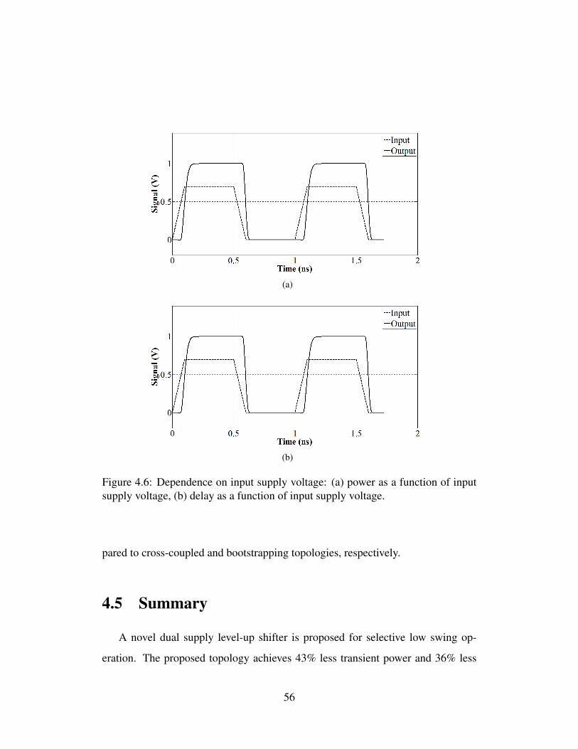
(a)
(b)
Figure 4.6: Dependence on input supply voltage: (a) power as a function of inputsupply voltage, (b) delay as a function of input supply voltage.
pared to cross-coupled and bootstrapping topologies, respectively.
4.5 Summary
A novel dual supply level-up shifter is proposed for selective low swing op-
eration. The proposed topology achieves 43% less transient power and 36% less
56

leakage power than the most commonly used cross-coupled topology, while also
consuming 9.5% less area. As compared to bootstrapping technique, proposed
topology achieves 79.5% reduction in physical area. Corner simulations are also
performed, demonstrating the superior performance of the proposed level shifter.
57

Chapter 5
Exploiting Useful Skew in Gated Low
Voltage Clock Trees for High
Performance
Existing works on low swing/voltage clocking do not consider the performance
requirements of the IC. In practice, low swing clocking introduces two issues re-
lated to performance: 1) possible degradation in clock-to-Q delay of the flip-flops
due to low swing clock signal, 2) timing degradation in the Enable paths of a gated
clock network due to higher clock insertion delay. A possible solution to the first
issue is to restore the full swing/voltage operation before the clock signal reaches
flip-flops [24]. This approach reduces the power savings since the last stage of
a clock network has high switching capacitance. In Chapter 3, a novel flip-flop
topology has been proposed for low swing clock signals without any degradation
in clock-to-Q delay, addressing issue one. A methodology based on useful skew is
58

proposed in this chapter to address issue two.
Clock gating [74, 75] is a standard method to reduce dynamic power by deac-
tivating the clock signals of the idle flip-flops. Thus, proposed methods based on
low voltage/swing clocking should be able to consider clock gating. A simplified
gated clock network is shown in Fig. 2.13. The clock signal can be gated by an in-
tegrated clock gating (ICG) cell, depending upon the Enable signal. If the Enable
signal is active, the output of the ICG cell (gated clock signal) does not switch even
though the clock signal switches, thereby reducing dynamic power in certain clock
nets. Unfortunately, a low voltage/swing clock signal degrades the timing of the
Enable path even when the data signals are at nominal voltage, as further described
in Section 5.1.3.
A useful skew approach is formulated in this chapter for gated clock networks
operating at a reduced voltage. The methodology is evaluated on largest ISCAS’89
benchmark circuits, demonstrating that the useful skew can effectively fix timing
violations (introduced due to low voltage/swing operation) within the Enable paths.
The rest of this chapter is organized as follows. Background on low swing op-
eration and problem formulation are provided in Section 5.1. The proposed method
is described in Section 5.2. Experimental results on several large ISCAS’89 bench-
mark circuits are presented in Section 5.3. The chapter is concluded in Section 5.4.
59

5.1 Background on Low Swing Operation and Prob-
lem Formulation
Historically, the clock skew is managed in three ways: i) zero skew, ii) bounded
skew and iii) useful skew approaches, i.e., clock skew scheduling. The zero skew
and bounded skew approaches ensure that the clock arrival time of all of the sequen-
tial elements is either identical (for zero skew) or within a margin (for bounded
skew). Alternatively, the useful skew approach considers clock skew scheduling
where the skew of each sequential element that belongs to the same timing path
is individually considered for timing optimization. In clock skew scheduling, the
available timing slack at each sequential element is utilized to improve clock pe-
riod of the IC. Specifically, slower data paths “borrow” time from faster data paths.
Thus, skew scheduling exploits the mismatches in the timing characteristics of the
data paths to decrease clock period.
Conventional clock skew scheduling techniques rely on linear programming
(LP) with a minimum clock period objective [11, 76, 77] or a graph-based solution
to utilize existing graph algorithms [78,79]. In [80], delay insertion methodology in
clock skew scheduling is proposed. In [81], a linear programming approach is pro-
posed to minimize the overall delay insertion while maintaining the minimum clock
period. In order to mitigate the effect process variations on skew, multi-domain
clock skew scheduling [82] is proposed. In [83, 84], two optimal algorithms are
developed to implement a multi-domain clock skew scheduling.
Traditional clock skew scheduling is briefly summarized in Section 5.1.1. Unique
challenges introduced due to clock gating are discussed in Section 5.1.2. Enable
path timing in low swing operation is introduced in Section 5.1.3.
60

Figure 5.1: Simple sequential circuit consisting of three registers without clockgating.
5.1.1 Traditional Clock Skew Scheduling
In a sequential timing path P, assume Ri and R j represent two registers, ti and
t j are clock arrival times for registers Ri and R j, respectively. For each data path
P in the circuit, two types of timing constraints exist: setup time (max delay) and
hold time (min delay) constraints, which are represented, respectively, by (5.1) and
(5.2),
ti− t j ≤ T −DPmax, (5.1)
ti− t j ≥−DPmin, (5.2)
where T is the clock period, DPmax and DPmin are the maximum and minimum data
path delays that include setup and hold time, respectively [62].
A simple sequential circuit with three registers R1, R2 and R3 and without clock
gating is shown in Fig. 5.1. Two buffers B1 and B2 are inserted at the primary
input and the output load, respectively. A pair of delay values (Dmin,Dmax) is de-
noted with each buffer, where Dmin,bu f and Dmax,bu f are the minimum and maximum
propagation delay of the buffer, respectively. There are two data paths in this cir-
cuit, R1→ R2 and R2→ R3, which are also associated with a pair of delay values
(DPmin,path,DPmax,path) representing minimum and maximum data path delays.
Conventional clock skew scheduling approaches find a set of clock arrival times
61

LP based formulationObjective: min T1 −12≤ t1− t2 ≤ T −162 −10≤ t2− t3 ≤ T −133 −2≤ thost− t1 ≤ T −44 −5≤ t3− thost ≤ T −75 0≤ t1, t2, t3, thost ≤ T
Table 5.1: LP based formulation of skew scheduling for the simple circuit shown inFig. 5.1.
corresponding to each register, which should satisfy each data path’s timing con-
straints represented by (5.1) and (5.2). In [76], the proposed clock skew scheduling
methodology is formulated as a simple linear programming (LP) problem where the
objective function is to minimize the clock period. The linear programming model
of the motivational example shown in Fig. 5.1 is listed in Table 5.1. Lines 1 to 4
represent the timing constraints of the two data paths and the primary input and the
primary output paths. Line 5 is included to limit the maximum global skew within
one clock period. The linear programming determines the minimum clock period as
10 units with the following set of skew schedule: t1 = 0, t2 = 6, t3 = 9 and thost = 6.
In addition to utilizing linear programming to perform clock skew scheduling, a
sequential circuit can also be modeled as a constraint graph G(V,E), in which each
vertex represents a register and two edges (with opposite directions) connecting two
vertices represent setup and hold time constraints, respectively. In [79], a constraint
graph based approach is proposed to optimize clock skew. In this graph-based
approach, each data path from Ri to R j in a sequential path has two edges: 1) an
edge (R j,Ri) with weight T −DPmax models the setup time constraint in (5.1) and
62
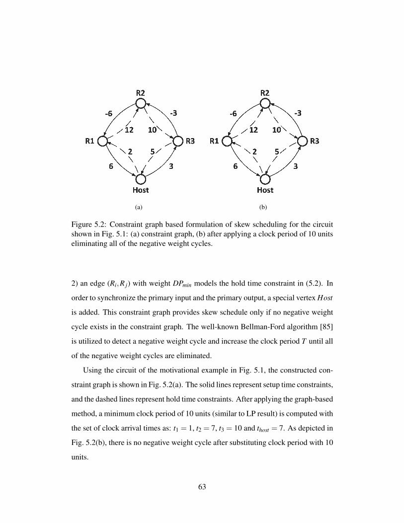
(a) (b)
Figure 5.2: Constraint graph based formulation of skew scheduling for the circuitshown in Fig. 5.1: (a) constraint graph, (b) after applying a clock period of 10 unitseliminating all of the negative weight cycles.
2) an edge (Ri,R j) with weight DPmin models the hold time constraint in (5.2). In
order to synchronize the primary input and the primary output, a special vertex Host
is added. This constraint graph provides skew schedule only if no negative weight
cycle exists in the constraint graph. The well-known Bellman-Ford algorithm [85]
is utilized to detect a negative weight cycle and increase the clock period T until all
of the negative weight cycles are eliminated.
Using the circuit of the motivational example in Fig. 5.1, the constructed con-
straint graph is shown in Fig. 5.2(a). The solid lines represent setup time constraints,
and the dashed lines represent hold time constraints. After applying the graph-based
method, a minimum clock period of 10 units (similar to LP result) is computed with
the set of clock arrival times as: t1 = 1, t2 = 7, t3 = 10 and thost = 7. As depicted in
Fig. 5.2(b), there is no negative weight cycle after substituting clock period with 10
units.
63
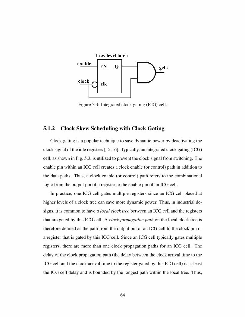
Figure 5.3: Integrated clock gating (ICG) cell.
5.1.2 Clock Skew Scheduling with Clock Gating
Clock gating is a popular technique to save dynamic power by deactivating the
clock signal of the idle registers [15,16]. Typically, an integrated clock gating (ICG)
cell, as shown in Fig. 5.3, is utilized to prevent the clock signal from switching. The
enable pin within an ICG cell creates a clock enable (or control) path in addition to
the data paths. Thus, a clock enable (or control) path refers to the combinational
logic from the output pin of a register to the enable pin of an ICG cell.
In practice, one ICG cell gates multiple registers since an ICG cell placed at
higher levels of a clock tree can save more dynamic power. Thus, in industrial de-
signs, it is common to have a local clock tree between an ICG cell and the registers
that are gated by this ICG cell. A clock propagation path on the local clock tree is
therefore defined as the path from the output pin of an ICG cell to the clock pin of
a register that is gated by this ICG cell. Since an ICG cell typically gates multiple
registers, there are more than one clock propagation paths for an ICG cell. The
delay of the clock propagation path (the delay between the clock arrival time to the
ICG cell and the clock arrival time to the register gated by this ICG cell) is at least
the ICG cell delay and is bounded by the longest path within the local tree. Thus,
64

each ICG cell is associated with a lower and upper bound of clock propagation path
delay.
Figure 5.4: Simple sequential circuit consisting of an ICG cell, two registers gatedby this ICG cell, a local clock sub-tree, and a timing loop formed by clock propa-gation path and clock enable path.
A simplified motivational example with clock gating is shown in Fig. 5.4 to
better illustrate the aforementioned definitions. For simplicity, the circuit in this
example has one ICG cell ICG1, gating two registers R1 and R2. A local sub-tree
including two buffers B5 and B6 is synthesized to drive the two registers. Each
buffer is denoted with a pair of delay values, which indicates the minimum and the
maximum clock propagation path delays. The clock enable (or control) path is from
R1 to ICG1 and consists of a single combinational gate, C1. Note that for simplicity,
data paths are omitted in this example so that the issues related with clock gating
can be emphasized.
Conventional clock skew scheduling methodologies cannot consider the unique
challenges introduced by clock gating. In [86], the authors have recently proposed
a linear programming approach to investigate the clock gated designs. In this work,
65

useful skew is utilized in a gated design via considering both the data paths and
clock enable paths with the objective function of minimum insertion delay [86].
However, it is assumed that the clock arrival time to an ICG cell is the same as the
clock arrival time to the registers gated by this ICG. This assumption is impractical
since in practice, the clock signal is distributed with a local clock tree that has larger
and non-identical clock propagation delays (as depicted in Fig. 5.4). A method
to perform clock skew scheduling in clock gated design with a local sub-tree is
described in Section 5.2.
5.1.3 Low Swing Operation
In gated clock networks, each ICG cell creates a timing path for the Enable
signals. Note that an ICG cell consists of a latch, as shown in Fig. 5.3. Unlike
conventional data paths, the output of an Enable path is a clock signal. In practice,
an ICG cell can drive a large number of flip-flops. Thus, it is common to have a
local clock tree between the ICG and the sinks driven by this ICG. In Fig. 5.4, this
local tree is simply represented by buffer B5 and B6.
When the clock voltage is reduced, the delay from ICG to the flip-flops (R2-R5)
increases. Thus, clock signal arrives at ICG much earlier than the sinks R2-R5.
Assuming negligible clock skew, clock signal arrives at R1 at approximately the
same time as R2-R5. Thus, clock signal arrives at ICG (capturing latch of the
Enable path) earlier than the R1 (launching flip-flop of the Enable path). Thus, the
timing slack of the Enable path is reduced by this difference. This issue places a
practical limitation on low voltage clocking if performance needs to be maintained.
To better illustrate this issue, signal waveforms at different clock nets and Enable
signal are shown in Figure 5.5, assuming zero clock skew. During the second clock
66

Figure 5.5: Timing graph of the gated clock network shown in Fig. 2.13.
period, Enable signal changes. Referring to this figure, the Enable paths should
satisfy the following max delay constraint,
tEN + tICG setup + tclock propagation < Tclock, (5.3)
where tEN , tICG setup and tclock propagation are, respectively, Enable path delay, ICG
cell setup time, and clock propagation delay within the local clock tree. The sum of
these three variables should be less than one clock period. Since clock signal should
always arrive at the ICG cell earlier than the flip-flops gated by this ICG cell (de-
termined by tclock propagation that is always positive), the timing slack of the Enable
path is reduced. In low swing operation, due to the increase in clock buffer de-
lays, clock propagation delay tclock propagation increases. Thus, the reduction in the
timing slack of the Enable path is more pronounced. The proposed linear program-
ming based useful skew methodology makes low swing operation more practical
by alleviating this timing degradation of the Enable paths.
67
5.2 Proposed Approach
Since ICG cell has a clock pin, in the proposed approach, each ICG cell is
treated as a register with an associated clock arrival time. Since there is a local
clock tree between an ICG cell and registers gated by this ICG, the associated clock
propagation delays can be treated as clock skew. However, note that the clock
signal should arrive to the ICG cell earlier than it arrives to the registers gated
by this ICG cell due to positive clock propagation path delay. This constraint is
different than conventional data paths where skew can be both positive and negative.
Two different objectives are considered: (1) maximize circuit performance and (2)
increase Enable path slack. These approaches are introduced in Section 5.2.1 and
Section 5.2.2, respectively.
5.2.1 Maximizing Circuit Performance
The linear programming based solution to skew scheduling in gated clock trees
is described in Section 5.2.1.1 whereas the constrained graph based approach is
discussed in Section 5.2.1.2.
5.2.1.1 Linear Programming
The arrival time of a clock signal to a register gated by an ICG cell is larger than
the arrival time of the clock signal to the ICG cell (see Fig. 5.4). The lower bound
for each clock propagation path delay is determined by the AND gate delay and a
local clock tree. This inequality is given by,
ticg, j− ti ≤−CPmin, (5.4)
68

LP based approach for ICs with clock gatingObjective: min T1 ti− t j ≥−DPmin(data path)2 ti− t j ≤ T −DPmax(data path)3 ticg, j− ti ≥−CPmax (propagation path)4 ticg, j− ti ≤−CPmin (propagation path)5 ti− ticg, j ≥−EPmin (enable path)6 ti− ticg, j ≤ T −EPmax (enable path)7 0≤ ti, ticg, j ≤ T
Table 5.2: LP based approach to clock skew scheduling in a clock gated design.
where ticg, j and ti are the clock arrival times to ICG cell ICG j and register Ri, re-
spectively. CPmin is the minimum clock propagation path delay.
An upper bound on clock propagation path delay is also required to represent
the maximum delay of the local clock tree,
ti− ticg, j ≤CPmax, (5.5)
where CPmax is the maximum delay of the corresponding clock propagation path.
Combining the constraints in (5.4) and (5.5) with the traditional, data path related
constraints, an improved linear programming solution for skew scheduling in ICs
with gated clock trees is obtained, as listed in Table 5.2. The bold lines represent
the new constraints required for gated clock networks.
The first two lines are the data path related constraints whereas lines 3 and 4
are the constraints related with clock propagation paths. Lines 5 and 6 represent
the timing constraints of the enable (control) path. Line 7 is added to limit the
global skew within one clock period. The linear programming based solution for
69

LP based approach for ICs with clock gatingObjective: min Ts.t. −3≤ thost− t1 ≤ T −5
−2≤ thost− t2 ≤ T −5−2≤ thost− t3 ≤ T −5−5≤ t2− thost ≤ T −7−3≤ ticg,1− t2 ≤−1−4≤ ticg,1− t3 ≤−2−11≤ t1− ticg,1 ≤ T −15−14≤ t3− ticg,1 ≤ T −200≤ t1, t2, t3, ticg,1, thost ≤ T
Table 5.3: Application of the LP based approach to circuit shown in Fig. 5.4.
the motivational example in Fig. 5.4 is listed in Table 5.3. The program determines
the minimum clock period as 22 units and a set of clock arrival times as t1 = 0,
t2 = 1, t3 = 2, ticg,1 = 0, and thost = 0.
5.2.1.2 Constraint Graph
In addition to linear programming, constraint graph based solution is also pro-
posed to compare the efficacy and confirm the accuracy of the proposed methods.
Each ICG cell is treated as a register and added to the directed graph as a vertex. The
maximum and minimum clock propagation path delays are treated, respectively, as
setup and hold time constraints of a traditional data path. Specifically, (5.4) is
treated as a setup time constraint and modeled by a directed edge (Ri, ICG j) with
weight −CPmin. Similarly, (5.5) is treated as a hold time constraint and modeled by
a directed edge (ICG j,Ri) with weight CPmax.
An important issue in graph based solution of skew scheduling in gated clock
70

Figure 5.6: Simple example to illustrate the timing loop formed by an ICG cell anda register gated by this ICG cell.
(a) (b) (c)
Figure 5.7: Constraint graph of the circuit shown in Fig. 5.6: (a) original graph, (b)after one iteration with clock period as 11 units, (c) after breaking the timing loop.
networks is a possible timing loop that can form between an ICG cell and one of
the registers gated by this ICG cell. Assume that the enable signal of the ICG cell
is provided from the output pin of one of the registers that is gated by the same ICG
cell (such as ICG1 and R3 in Fig. 5.4), then the ICG cell and the register form a
loop. Unlike conventional data paths, the clock signal should arrive to the register
later than it arrives to the ICG. Thus, this timing loop should be broken from the
directed graph while still maintaining accurate results. As observed from experi-
mental results on ISCAS’89 benchmark circuits, breaking the loop is necessary to
obtain a feasible skew schedule.
71
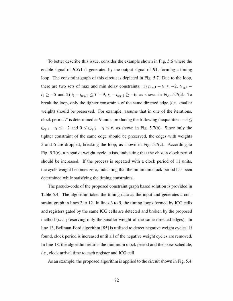
To better describe this issue, consider the example shown in Fig. 5.6 where the
enable signal of ICG1 is generated by the output signal of R1, forming a timing
loop. The constraint graph of this circuit is depicted in Fig. 5.7. Due to the loop,
there are two sets of max and min delay constraints: 1) ticg,1− t1 ≤ −2, ticg,1−
t1 ≥ −5 and 2) t1− ticg,1 ≤ T − 9, t1− ticg,1 ≥ −6, as shown in Fig. 5.7(a). To
break the loop, only the tighter constraints of the same directed edge (i.e. smaller
weight) should be preserved. For example, assume that in one of the iterations,
clock period T is determined as 9 units, producing the following inequalities: −5≤
ticg,1− t1 ≤ −2 and 0 ≤ ticg,1− t1 ≤ 6, as shown in Fig. 5.7(b). Since only the
tighter constraint of the same edge should be preserved, the edges with weights
5 and 6 are dropped, breaking the loop, as shown in Fig. 5.7(c). According to
Fig. 5.7(c), a negative weight cycle exists, indicating that the chosen clock period
should be increased. If the process is repeated with a clock period of 11 units,
the cycle weight becomes zero, indicating that the minimum clock period has been
determined while satisfying the timing constraints.
The pseudo-code of the proposed constraint graph based solution is provided in
Table 5.4. The algorithm takes the timing data as the input and generates a con-
straint graph in lines 2 to 12. In lines 3 to 5, the timing loops formed by ICG cells
and registers gated by the same ICG cells are detected and broken by the proposed
method (i.e., preserving only the smaller weight of the same directed edges). In
line 13, Bellman-Ford algorithm [85] is utilized to detect negative weight cycles. If
found, clock period is increased until all of the negative weight cycles are removed.
In line 18, the algorithm returns the minimum clock period and the skew schedule,
i.e., clock arrival time to each register and ICG cell.
As an example, the proposed algorithm is applied to the circuit shown in Fig. 5.4.
72

Graph based approach (timing data)1: start with a clock period T2: for each edge(u,v) with weight w3: if (u,v) ∃ in G(V,E)4: if weight(u,v)>w5: weight(u,v)=w6: else7: add edge(u,v)8: end for9: add a source node10: for each V ∈ G(V,E) except source node11: add edge(source,V) with weight T12: end for13: apply Bellman-Ford algorithm on G(V,E)14: if ∃ negative weight cycle15: increase clock period16: repeat Line 1-1317: else18: return clock period T and skew schedule
Table 5.4: Graph based solution for ICs with clock gating, including the proposedmechanism to break the timing loop.
(a) (b) (c)
Figure 5.8: Constraint graph of the circuit shown in Fig. 5.4: (a) original graph, (b)after one iteration with clock period as 22 units, (c) after breaking the timing loop.
73

The original constraint graph that corresponds to this circuit is depicted in Fig. 5.8(a).
T is replaced with the minimum clock period 22 units, producing the graph shown
in Fig. 5.8(b). The timing loop formed by ICG1 and D3 are broken using the pro-
posed method, producing the final graph shown in Fig. 5.8(c). The algorithm returns
the clock arrival times as t1 = 22, t2 = 22, t3 = 22, ticg = 20, and thost = 22.
5.2.2 Increasing Timing Slack of EEEnnnaaabbbllleee Paths
LP based approach for ICs with clock gatingInputs: path delays and clock periodOutputs: skew scheduleObjective: max Σ(treg,i− ticg, j) for each j1 ti− t j ≥−DPmin(data path)2 ti− t j ≤ T −DPmax(data path)3 ticg,j− ti ≥−CPmax(propagation path)4 ticg,j− ti ≤−CPmin(propagation path)5 ti− ticg,j ≥−EPmin(Enable path)6 ti− ticg,j ≤ T−EPmax(Enable path)7 0≤ ti, ticg, j ≤ T
Table 5.5: Proposed LP based approach to exploit useful skew in low swing opera-tion.
The previous section provided a framework to achieve skew scheduling in gated
clock trees. In this section, this framework is utilized to exploit useful skew in
increasing the timing slack of the Enable paths. As described earlier, in gated low
voltage clock trees, the Enable paths suffer from reduced timing slack. In this
section, the objective function of the LP is to maximize the ICG-to-DFF delay,
thereby increasing the timing slack of the Enable paths, as shown in Table 5.5. In
74

other words, more delay can be tolerated between ICG and flip-flops.
The linear programming based solution for the motivational example in Fig. 5.4
is listed in Table 5.6 after substituting clock period with 22 time units. The program
determines a set of clock arrival times as t1 = 8, t2 = 22, t3 = 21, ticg,1 = 19, and
thost = 20, where ICG1 to R2 delay increases from 1 to 3 time units, whereas ICG1
to R3 delay remains the same as 2 time units.
LP based approach for ICs with clock gatingObjective: max (t2− ticg,1+t3− ticg,1)s.t. −3≤ thost− t1 ≤ 17
−2≤ thost− t2 ≤ 17−2≤ thost− t3 ≤ 17−5≤ t2− thost ≤ 15−3≤ ticg,1− t2 ≤−1−4≤ ticg,1− t3 ≤−2−11≤ t1− ticg,1 ≤ 7−14≤ t3− ticg,1 ≤ 20≤ t1, t2, t3, ticg,1, thost ≤ 22
Table 5.6: Application of the LP based approach to circuit shown in Fig. 5.4 toincrease the timing slack of the Enable paths.
5.3 Experimental Results
5.3.1 Circuit Performance
The proposed LP based and constraint graph based approaches for skew schedul-
ing in gated clock networks are evaluated using the largest ISCAS’89 benchmark
circuits consisting of up to approximately 2000 registers. Each benchmark is syn-
75
thesized with Synopsys Design Compiler [87] using the 45 nm NanGate open cell
library [88]. ICG cells are inserted by the tool during the synthesis stage. An open
source GLPK (GNU Linear Programming Kit) [89] is used as the linear program-
ming solver, running on a Linux system with Intel Xeon processor.
The experimental results are listed in Table 5.7 for both linear programming and
graph based solutions. It is important to note that both solutions provide the same
minimum clock period in each circuit, verifying the accuracy of the algorithms.
The maximum reduction in clock period after skew scheduling is approximately
21%, which highly depends upon the timing data. In some benchmarks, higher
gating percentage corresponds to less reduction in clock period, such as S1423 and
S38417. However, this behavior does not hold in other benchmarks such as S38584
where 16% reduction in clock period is achieved with approximately 72% gating.
It is also shown in Table 5.7 that the graph based solution produces smaller global
skew than LP based solution.
The run time of both solutions is compared in Fig. 5.9 for some of the bench-
mark circuits. LP based solution runs faster than or equal to graph based solution.
Note that the graph based approach utilizes Bellman-Ford algorithm with a compu-
tational complexity of O(V ·E) [85], where V is the overall number of registers and
ICG cells in the circuit, and E is the overall number of data paths, Enable paths and
clock propagation paths. Lines 2 to 8 in Table 5.4 have a complexity of O(E) and
lines 9 to 11 have a complexity of O(V ). Therefore, the computational complexity
of the graph based method is maintained at O(V ·E). The LP based solution utilizes
the simplex algorithm and in practice, runs faster. However, note that with certain
inputs, simplex algorithm may require exponential time to reach a solution [85].
76
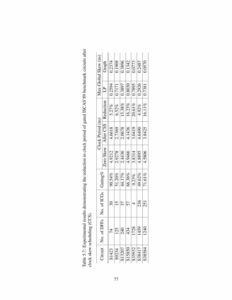
Tabl
e5.
7:E
xper
imen
talr
esul
tsde
mon
stra
ting
the
redu
ctio
nin
cloc
kpe
riod
ofga
ted
ISC
AS’
89be
nchm
ark
circ
uits
afte
rcl
ock
skew
sche
dulin
g(C
CS)
.
Cir
cuit
No.
ofD
FFs
No.
ofIC
Gs
Gat
ing%
Clo
ckPe
riod
(ns)
Max
Glo
balS
kew
(ns)
Zer
oSk
ewA
fter
CSS
Red
uctio
nL
PG
raph
S142
374
3090
.54%
4.92
124.
6618
5.27
%0.
2594
0.23
74S9
234
125
1551
.20%
2.92
782.
7369
6.52
%0.
7171
0.19
09S1
3207
240
3744
.17%
2.44
362.
0678
15.3
8%0.
3897
0.38
96S1
5850
434
5766
.36%
4.94
664.
1436
16.2
3%0.
8030
0.13
42S3
5932
1728
40.
23%
3.83
143.
0419
20.6
1%0.
7895
0.07
73S3
8417
1459
236
49.6
2%4.
8895
4.64
904.
92%
0.29
260.
2487
S385
8412
4025
171
.61%
4.58
063.
8425
16.1
1%0.
7381
0.05
70
77

Figure 5.9: The runtime comparison of linear programming and graph based ap-proaches.
5.3.2 Timing Slack of EEEnnnaaabbbllleee Paths
The proposed useful skew approach to facilitate low swing clocking without
degrading the timing slack of the Enable paths is evaluated with the same software
setup as in maximizing circuit performance. The longest runtime is 120 seconds for
s38417.
The experimental results comparing the zero skew and useful skew are listed in
Table 5.8. Both zero skew and useful skew cases operate at the same clock period
which is the minimum clock period in zero skew. Depending upon the mismatch in
the data paths, up to 86% improvement in Enable slack can be achieved. On aver-
age, the slack of the Enable path is increased by 47% after applying the proposed
useful skew approach.
The maximum ICG-to-DFF delays are listed in Table 5.9 when the clock period
is the minimum theoretical clock period after useful skew. If the proposed useful
78

CircuitClock Period Max ICG-to-DFF Delay (ns) Increase in
(ns) Zero Skew Useful Skew Enable Slacks13207 2.71 2.13 2.36 10.8%s15850 4.93 2.78 3.72 33.8%s35932 3.83 1.20 2.24 86.7%s38417 4.85 3.47 4.85 39.8%s38584 4.61 2.12 3.48 64.2%
Table 5.8: Experimental results demonstrating the increase in the slack of theEnable paths after exploiting useful skew.
CircuitMin Clock Period Max ICG-to-DFF Delay Run Time
(ns) (ns) (s)s13207 2.26 1.91 0s15850 4.13 2.91 5s35932 3.04 1.45 7s38417 4.66 4.56 120s38584 4.04 2.92 25
Table 5.9: Experimental results demonstrating the increase in the slack of theEnable paths after exploiting useful skew at the minimum clock period.
skew approach is adopted in this case, the maximum ICG-to-DFF delays are de-
graded on average, by 20% as compared to the useful skew case in Table 5.8 (with
a larger clock period). This result is expected since in Table 5.9, there is a tighter
constraint for clock period.
5.4 Summary
A useful skew approach in clock-gated network is proposed in this chapter to
maximize the circuit performance and increase the timing slack of Enable path,
which facilitates low swing clocking. It is evaluated on ISCAS’89 benchmark cir-
79

cuits with clock gating cell inserted automatically by Synopsys Design Compiler.
Experimental results demonstrate up to approximately 21% reduction in clock pe-
riod and 47% increase in the timing slack of the Enable path.
80

Chapter 6
Slew-Driven Clock Tree Synthesis
Methodology
The design process for clock distribution networks is directly affected by tech-
nology (i.e. interconnect and transistor) scaling [5, 11, 90]. The impact of technol-
ogy scaling on clock skew is well-understood and the skew constraint is satisfied
with various existing clock tree synthesis (CTS) algorithms [28, 91–97]. Alter-
natively, the methodical investigation of clock slew is primarily unaddressed. In
particular, the increase in the interconnect resistance makes it more challenging to
satisfy slew constraints on long wires. Furthermore, voltage scaling is a popular
method for power management, which also exacerbates clock slew.
Despite the well-understood detrimental effects of interconnect resistance and
low voltage operation on clock slew, using clock slew as a driving factor for clock
tree synthesis has not been investigated. In [95], an obstacle-avoiding and slew-
constrained clock tree synthesis methodology with efficient buffer insertion is pro-
81
posed, where clock skew and latency are enhanced. In [96], a fast power- and slew-
aware gated clock tree synthesis methodology is proposed with zero skew. In [29],
a variation-aware clock network design methodology is proposed for ultra-low volt-
age circuits, where both clock skew and slew are controlled to maximize the circuit
performance. In [27], a systematic approach is proposed to design the clock tree
for subthreshold circuits to reduce the clock slew variations while minimizing the
energy dissipation in the tree. Exploiting slew-awareness as part of the clock tree
synthesis (i.e. slew-driven) has not been previously addressed.
A slew-driven CTS methodology called SLECTS is proposed in this chapter.
SLECTS can satisfy aggressive slew constraints that are significantly more chal-
lenging for traditional delay/skew-driven CTS methodologies.
Instead of targeting skew minimization as the primary objective and resolving
slew violations with buffer insertion with a capacitance or slew bound, as in tra-
ditional skew-driven CTS, SLECTS targets slew optimization at each stage of the
synthesis, such as clustering (i.e. merging) clock tree nodes, defining routing points
and handling long interconnects. A typical approach in existing CTS techniques is
to perform skew minimization in the first stage and resolve slew violations during
post-CTS optimization [98]. Skew-driven CTS uses buffering and sizing to con-
strain only skew during the CTS process, and uses additional buffering and sizing
post-CTS to remove slew violations. Alternatively, SLECTS uses buffering and
clustering more efficiently to simultaneously constrain skew and slew. Due to this
efficient slew handling and efficient use of buffering, SLECTS leads to reduced
power dissipation while satisfying the slew and skew constraints. The proposed
slew-driven CTS methodology exhibits the following innovations: 1) a new merg-
ing point computation method, 2) a new method to simultaneously check and satisfy
82
skew and slew, 3) a new cost metric for the merging process, 4) a new net splitting
method, which is essential for clock trees with long interconnects.
Merging point computation and cost metric novelties help reducing the power
consumption compared to existing methods. In addition, SLECTS is significantly
more successful in satisfying tighter slew constraints at lower operating voltages.
Thus, SLECTS not only enables clock signals with higher frequencies (where slew
constraints are tighter) to be reliably distributed, but also accomplishes this distri-
bution with reduced power consumption.
Experimental results on an industrial circuit with more than 1 million gates in
28 nm FDSOI technology demonstrate that, at the slow process, voltage, tempera-
ture corner, SLECTS satisfies tight slew constraint of 60 ps whereas a commercial
CTS tool not only violates the slew constraint, but also consume 8% more clock
power. At the scaled 0.8 V operation, SLECTS satisfies the slew constraint with
approximately 15% less clock power while achieving a similar skew constraint.
The experimental results demonstrate that SLECTS methodology can be combined
with the proposed low swing flip-flop topology (see Chapter 3) to produce a low
swing/voltage clock tree with up to 48% reduction in clock power.
The rest of this chapter is organized as follows. Five proposed techniques for
the slew-driven clock tree synthesis methodology are introduced in Section 6.1.
Experimental results of the proposed methodology are presented in Section 6.2.
The power analysis of combining SLECTS and low swing flip-flop is provided in
Section 6.3. Finally, the chapter is concluded in Section 6.4.
83

6.1 Slew-Driven Clock Tree Synthesis Algorithm
Deferred merge embedding (DME) method is a popular framework used for
clock tree synthesis in the literature [43, 44, 93]. The proposed methodology, de-
veloped within the DME framework, is illustrated in Fig. 6.1 with a flowchart. The
slew driven novelties in SLECTS are highlighted with labels Step 1, Step 2, Step 3,
Step 4 and Step 5. In particular, SLECTS consists of 5 novel contributions:
1. A slew- and skew-aware merging point computation method (Step 1),
2. Checking and satisfying skew using a single or multiple buffers (Step 2),
3. Checking and satisfying slew using buffer sizing (Step 3),
4. A pair selection and cost metric definition considering physical distance for
efficient sink clustering (Step 4),
5. A slew- and insertion delay-aware net splitting (Step 5).
These five steps are described in Sections 6.1.1 to 6.1.5. Time complexity and
runtime of the proposed method are discussed and compared with a commercial
tool in Section 6.1.6.
6.1.1 Step 1: Merging Point Computation
In traditional DME method, the algorithm searches every pair i− j from the
unmerged nodes to find feasible pairs to merge. A merging point is calculated
for each such pair i− j as a virtual routing point. A common practice [94] is
to select a specific point for merging considering skew, using the zero-skew-tree
DME (ZST-DME) algorithm [43,44]. Another approach proposed in [47] develops
a bounded-skew-tree DME (BST-DME) to define merging regions considering the
84

skew- and slew-aware merging
point computationStep 1
foreach(i,j)
satisfyskew?
calculatebuffer sizes
and locationsto fix skew
Step 2
satisfyslew?
calculatebuffer sizeto fix slew
Step 3
update cost metricslewfixed?
next(i,j) pair
feasiblepairsexist?
merge pairwith min cost
Step 4
#unmerged== 1?
DONE
net-splitting
Step 5
nextiteration
no
yes
no
yes
yes
no end of for loop
yes
yesno
no
Figure 6.1: The flowchart of SLECTS. The blue boxes are executed in everyf oreach loop, and the red boxes are executed after an iteration of f oreach loopis finished.
85
skew constraint during the bottom-up phase, and chooses the minimum wirelength
point at each region during the top-down phase. This early approach is applicable
only in “unbuffered” clock routing. In practice (and literature), buffered clock tree
routing has long been the norm [94, 99, 100], particularly when satisfying the slew
constraint is critical. Another practice is to use ZST-DME or BST-DME approaches
as a first step, while allowing slew violations, and consider buffering as an added
optimization step to remove violations. In slew-driven buffering, computing merg-
ing regions at each iteration of the bottom-up phase is computationally expensive
due to the highly complex slew estimation equation (introduced in Section 6.1.1).
Furthermore, permitting slew violations results in decisions based on inaccurate(ly
high) slew on the nodes with violations.
In this thesis, the skew constraint-based merging regions are constructed during
the bottom-up phase, similar to the BST-DME methodology [47]. Unlike BST-
DME methodology where merging regions are propagated during the bottom-up
phase and the merging points are determined during the top-down phase, the merg-
ing point is determined within this merging region considering the slew constraint
during the same phase. This is an algorithmic change from traditional approaches
in order to simultaneously satisfy skew and slew constraints. This process requires
a novel definition for permissible merging window to satisfy the skew constraints,
and cross-referencing this window with a minimum slew point to satisfy the slew
constraint.
86
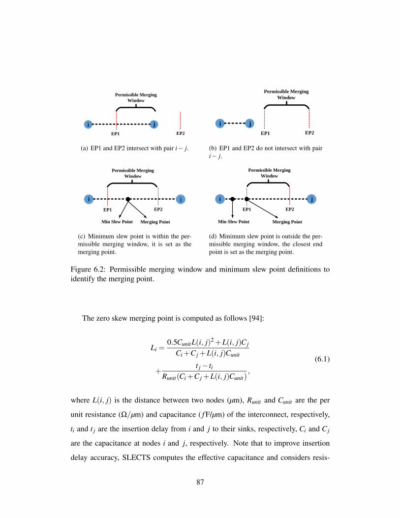
Permissible Merging
Window
i j
EP1 EP2
(a) EP1 and EP2 intersect with pair i− j.
Permissible Merging
Window
i j
EP1 EP2
(b) EP1 and EP2 do not intersect with pairi− j.
Permissible Merging
Window
i j
EP1 EP2
Min Slew Point Merging Point
(c) Minimum slew point is within the per-missible merging window, it is set as themerging point.
Permissible Merging
Window
i j
EP1 EP2
Min Slew Point Merging Point
(d) Minimum slew point is outside the per-missible merging window, the closest endpoint is set as the merging point.
Figure 6.2: Permissible merging window and minimum slew point definitions toidentify the merging point.
The zero skew merging point is computed as follows [94]:
Li =0.5CunitL(i, j)2 +L(i, j)C j
Ci +C j +L(i, j)Cunit
+t j− ti
Runit(Ci +C j +L(i, j)Cunit),
(6.1)
where L(i, j) is the distance between two nodes (µm), Runit and Cunit are the per
unit resistance (Ω/µm) and capacitance ( f F/µm) of the interconnect, respectively,
ti and t j are the insertion delay from i and j to their sinks, respectively, Ci and C j
are the capacitance at nodes i and j, respectively. Note that to improve insertion
delay accuracy, SLECTS computes the effective capacitance and considers resis-
87

Algorithm 1 Merging Point Computation
1: Maxi = max[Dins(i)]2: Max j = max[Dins( j)]3: Mini = min[Dins(i)]+ skewconst4: Min j = min[Dins(i)]+ skewconst5: Compute EP1 by computing LEP1 with (6.1) for ti = Maxi, t j = Min j6: Compute EP2 by computing LEP2 with (6.1) for ti = Mini, t j = Max j7: Compute EP1 and EP2 intersection with pair i− j as permissible merging win-
dow8: Compute min slew point m by solving (6.4)9: if m ∈ permissible merging window then
10: Merging point k = m11: else if m < EP1 then12: Merging point k = EP113: else14: Merging point k = EP215: end if
tive shielding (based on [101]) to bi-linearly interpolate the look-up tables for each
clock buffer. As such, node capacitances Ci and C j in (6.1) represent the effective
capacitance.
The proposed merging point computation algorithm is presented in Algorithm 1.
For each pair i- j, the permissible merging window is defined based on the skew
constraint. As mathematically described in Algorithm 1, each end point (EP1 and
EP2) represents a corner case where the skew between i- j pair is equal to skew
constraint skewconst , and any point within the permissible merging window satisfies
this constraint (i.e. ≤ skewconst). In literature, there are studies that aim to choose
the middle of the permissible merging window as the merging point so as to increase
the robustness of delivered skew to variations [102]. In this work, the objective is to
simultaneously constrain skew and slew. As such, a slew-driven metric for merging
point computation is defined, as described below.
88
According to Algorithm 1, two skew corners and a permissible merging window
is generated along the axis of the i- j pair using (6.1) (Lines 5-7). The permissible
merging window is a line of potential merging points along which the skew con-
straint is satisfied. If the two skew corners EP1 and EP2 intersect with pair i− j, the
permissible merging window is set as the intersection, as shown in Fig. 6.2(a). Al-
ternatively, if the two skew corners are outside the pair i− j, as shown in Fig. 6.2(b),
the permissible merging window is set based on the two corners. In this case, buffer
insertion (when the delay mismatch is larger than one clock buffer delay) or wire
snaking (when the delay mismatch is smaller than one clock buffer delay) is ap-
plied to fix skew. Fixing skew with single/multiple buffer insertion is described in
Section 6.1.2. After the permissible merging window is generated, the minimum
slew point is computed (Line 8). The minimum slew point is defined as the point
that makes the slew at node i and j equal and minimum. In order to determine this
point, the PERI model [103] is used for slew propagation, which estimates the slew
degradation S(W ) on a wire segment W as:
S(W ) = ln(9)×ED(W ), (6.2)
where ED(W ) is the Elmore delay [104] of the wire segment W . The output slew
Sout(W ) of a wire segment W is estimated as:
Sout(W ) =√
Sin(W )2 +S(W )2, (6.3)
where Sin(W ) is the input slew of the wire segment. Using (6.2) and (6.3), the
89

minimum slew point m should satisfy the following equation:
S2i − (ln(9)×ED(m, i))2 = S2
j − (ln(9)×ED(m, j))2, (6.4)
where Si and S j are the target slew values at nodes i and j, respectively. The tar-
get slew values are set to slew constraint slewconst at the sink level, and they are
propagated bottom-up to the internal nodes after each merging. After (6.4) is re-
organized in a closed-form, it becomes a third-order equation (as Elmore delay
scales quadratically with wirelength). By using first-order derivative and analyzing
the monotonicity, one or multiple real roots can be found. If multiple real roots
exist, the root that generates the minimum skew between pair i− j is selected as
the minimum slew point m. If m is within the permissible merge window, it is set
as the merging point k, as shown in Fig. 6.2(c). Alternatively, if m is outside the
permissible window, the closest end point of the permissible window is set as the
merging point k (Line 11-14), as shown in Fig. 6.2(d).
6.1.2 Step 2: Fixing Skew Using Buffer Insertion
After computing the merging point for each pair i− j, as described in Sec-
tion 6.1.1, skew and slew constraints should be checked before determining the
feasible pairs to merge. Skew-driven CTS uses buffering and sizing during the
synthesis process to constrain clock skew. Since traditional DME-based CTS al-
gorithms consider buffer insertion at the merging point only, slew violation can
happen when the inserted buffer drives a long interconnect. These slew violations
are typically fixed with a post-CTS optimization in traditional methods.
SLECTS considers both slew and skew constraints while constructing the clock
90

L1 L2
i j
Single/multiple buffers
merging point
1 2 N
Figure 6.3: Illustration of fixing skew using single or multiple buffers and deter-mining the new merging point after fixing skew.
tree in a bottom-up manner. In cases where the permissible merge window does not
intersect with the i− j pair [see Fig. 6.2(b)], single or multiple buffers are inserted
and evenly distributed to fix skew (move the merge point between nodes i and j),
as depicted in Fig. 6.3.
If insertion delay mismatch between i− j is large or interconnect length be-
tween i− j is short, multiple buffers can be inserted. In this case, SLECTS dis-
tributes these buffers evenly while considering the capacitive load and maximum
drive ability of each buffer. In Fig. 6.3, the capacitive load of buffer 1 is the sum
of load at node i and the interconnect capacitance of wire length L1. For the re-
maining buffers, the capacitive load is the sum of buffer gate capacitance and the
interconnect capacitance of wire length L2. If node i exhibits a large capacitive
load, then the first buffer will be inserted sufficiently close to node i. This skew
fixing algorithm is shown in Algorithm 2. The proposed approach computes the
maximum interconnect length that each clock buffer in the library can drive, given
the buffer gate capacitance (Line 4). Then, the overall buffer and interconnect delay
is computed from node i with slew propagation from the input pin of last inserted
91

Algorithm 2 Fix Skew1: load f irst =Ci +CL12: loadother =Cgate +CL23: Find each type of buffer look-up tables4: Compute L1 and L25: Propagate slew from the input pin of last inserted buffer6: Dtotal = ∑each bu f f er(Dbu f f er +Dwire)7: if single buffer can fix the skew then8: return with buffer location and type9: else if multiple buffers can fix skew then
10: return with buffer locations and types11: else12: Find minimum skew with single/multiple buffers13: end if
buffer (Line 5-6). After the overall delay is calculated, a new merging point be-
tween last inserted buffer and node j is computed with the proposed merging point
computation algorithm described in Section 6.1.1. If single or multiple buffers can
fix the skew violation, then buffer locations and types are stored (Line 7-10). Al-
ternatively, if skew cannot be fixed by only inserting buffers, the minimum possible
skew is determined (Line 12).
6.1.3 Step 3: Fixing Slew Using Buffer Sizing
In traditional skew-driven CTS, slew violations are typically fixed during post-
CTS optimization. Since SLECTS targets slew optimization at every stage of the
clock tree synthesis, it checks slew constraint with buffer sizing after checking/fixing
skew violations with buffer insertion.
To satisfy the slew constraint for a specific pair i− j, a clock buffer is inserted at
the merging point to drive the capacitive load. The buffer sizing algorithm to satisfy
92

Algorithm 3 Fix Slew1: load =Ci +C j +Cwire2: for each usable buffer size k do3: Compute buffer output slew Slewout(bu fk)4: Propagate slew to i and j with (6.3)5: if Slewi ≤ SlewiReq&&Slew j ≤ Slew jReq then6: return buffer type k7: end if8: end for9: slew cannot be fixed
slew constraint is described in Algorithm 3. In Lines 1-3, overall capacitive load at
the buffer output pin is computed and the buffer output pin slew is determined using
look-up table of the specific buffer size k and bi-linear interpolation. Then, buffer
output pin slew is propagated to nodes i and j, using (6.3) (Line 4). Since slew
is propagated bottom-up, the slew requirement of node i and j is checked. If the
propagated slew from buffer output pin satisfies both node i and j slew requirement,
then the specific buffer size k can drive the load at the merging point. Otherwise, a
buffer with stronger drive capability is chosen (Line 5).
6.1.4 Step 4: Finding Feasible Pairs to Merge
According to Fig. 6.1, in SLECTS, no pairs are actually merged until after all
of the i− j pairs are visited and a related cost is determined for each pair. The
selection of pairs to merge and the cost definition significantly affect the quality of
results. Thus, several pair selection techniques and cost definitions were introduced
in the literature, which are classified into 2 groups: 1) distance-based [93], and
2) delay-based [94]. Distance-based approach considers the physical distance be-
tween two nodes as a cost metric, and merges minimum distance pairs. In terms of
93

accuracy, distance-based merging pair selection suffers from the deficiencies of us-
ing length as a delay metric. The time complexity of distance-based approach [93]
is O(nlogn), as merging is performed by selecting all minimum distance pairs in
one iteration. However, as the pairs are not selected one at a time, the merging of a
new node (created by a previous merging) with an existing node is not considered.
Thus, this selection results in a sub-optimal clustering.
The more contemporary and common cost definition is the delay-based ap-
proach, which achieves higher accuracy in terms of satisfying skew, the primary
objective of traditional skew-driven CTS algorithms. Delay is typically estimated
with Elmore delay, and common merging pair cost computations consider potential
wire-snaking between candidate nodes, as well. The delay-based approach in [94],
for instance, first identifies the candidate merging node with the maximum delay
target (i.e. candidate node with the minimum insertion delay from the node to the
clock sinks in its downstream). The approach then finds a minimum cost pair for
this node where cost is defined as the Elmore delay to a candidate pair node, includ-
ing the distance added to perform potential wire snaking. This approach provides
better skew results (compared to [93]), however, restricting the selection of the
minimum insertion delay node does not guarantee the minimum distance selection,
thereby degrading clock slew. In terms of algorithmic complexity, the maximum
delay target node and its minimum pair are identified with a linear search [both
O(n) complexity], resulting in a complexity of O(n2).
The contemporary and common delay-based cost definitions in the merging pair
selection has two drawbacks making them formidable for SLECTS: 1) Delay-based
cost results in pairing nodes that are physically farther to minimize skew, which is
detrimental to slew, 2) Considering wire snaking as part of cost metric is inaccurate.
94

Wire snaking is detrimental to slew, therefore, buffer insertion is a more viable
option for merging pairs that require significantly high wire snaking.
Consequently, in this thesis, a distance-based approach (similar to [93]) is se-
lected as the cost metric favoring reduced slew degradation along the path. It is
important to note here that using a distance-based cost results in several subtree
clusters that have different capacitance and delay values. This would make merging
more difficult at the top-level of a clock tree due to the insertion delay mismatches.
However, the potential effects of these mismatches are fixed by buffer insertion
and/or wire snaking, and the power overhead of these processes are shown, exper-
imentally, to be less than those necessary to fix slew following a traditional skew-
driven CTS application through DME.
In SLECTS, the distance-based cost metric for clustering (merging) nodes is
defined as the sum of distance (i.e. wire length) from calculated merging point (see
Section 6.1.1, Step 1) to node i and j (see Fig. 6.2). This change from traditional
DME-based CTS routines ensures satisfying both slew and skew constraints.
Algorithmically, the merging pair selection in SLECTS is performed by con-
sidering all of the possible pairs (up to n2 possibilities) at each iteration (see the
flowchart in Fig. 6.1). This theoretical O(n3) complexity of this selection scheme
is avoided with data re-use. In the first iteration, the costs of all n2 pairs of initial n
nodes are computed [complexity of O(n2)]. Starting from the second iteration, only
the costs of merging the recently added node against the other (n−1) nodes [O(n)]
are computed [complexity of O(n2)] as the other pairing combinations are already
computed in the first iteration. Thus, although the asymptotic complexity is still
O(n3), the algorithm performs O(n2) computations and O(n3) look-ups. It is shown
in Section 6.2 that the run time of the proposed methodology is significantly less
95

(a) A naive location-based net splitting. (b) The proposed insertion delay-aware netsplitting.
Figure 6.4: Demonstration of slew-aware net splitting.
than commercial CTS tools.
After finding the feasible pair, if merging this specific pair requires buffer in-
sertion to fix slew or skew (as determined in Steps 2 and 3), it affects the slew of
the downstream nodes. Therefore, a top-down slew propagation process is exe-
cuted and slew values are updated to improve slew estimation and insertion delay
accuracy.
6.1.5 Step 5: Slew-Aware Net Splitting
Traditional DME-based CTS algorithms consider buffer insertion only at the
merging points, and do not consider splitting the net (i.e. with buffering) after
selecting merging pairs. This approach produces slew violations on long intercon-
nects and do not permit the desired voltage and frequency scaling. Thus, existing
contemporary approach is to synthesize clock tree with slew violations and fix these
violations as a post-CTS optimization.
SLECTS satisfies slew constraints while considering the insertion delays of the
96

Algorithm 4 Net splitting1: Costcurr = ∞
2: for (i, j) in Unmerged nodes do3: if Cost(i, j)<Costcurr then4: Costcurr =Cost(i, j),si = i,s j = j5: end if6: end for7: if Dins(si)< Dins(s j) then8: Compute maximum interconnect length L with si9: else
10: Compute maximum interconnect length L with s j11: end if12: Generate new node m at the computed location
nodes to be merged. The purpose of considering insertion delays is to avoid a high
buffering and wire snaking cost that is induced due to large insertion delay mis-
match, and keep number of buffer levels balanced for process-voltage-temperature
(PVT) variations. In order to highlight this phenomenon, a motivational example is
illustrated in Fig. 6.4. It is assumed that three nodes i, j and k are to be merged and
a single buffer insertion cannot satisfy the slew constraint at neither of the nodes.
Thus, the net of the selected pair of nodes needs to be split with buffer insertion to
satisfy slew constraint. Assume that i- j pair has the lowest cost (i.e. minimum dis-
tance as defined in Section 6.1.4), and therefore is selected to be merged. A naive
approach, depicted in Fig. 6.4(a), could start splitting from node i in order to bring
the merging point closer to j and k for a lower merging cost in the next iteration.
However, this would significantly increase the insertion delay at node i, resulting
in excessive buffering and/or wire snaking when merging i with other nodes. The
insertion delay-aware net splitting technique, presented in Algorithm 4, is proposed
to address this issue. The proposed approach first finds the minimum cost pair (si
97
and s j in Line 4) and determines which node of the selected (i.e. minimum cost)
pair has a smaller insertion delay. Then, the distance is computed from this lower
insertion delay node (either si in Line 8 or s j in Line 10) to generate a new node
m (Line 12). Starting net splitting from the node that has a smaller insertion delay
provides a more balanced buffering, such as the one depicted in Fig. 6.4(b).
In the proposed approach, the splitting point is determined as the longest feasi-
ble distance from the selected (smaller insertion delay) node. The longest feasible
distance is computed using the slew constraint, the look-up tables of the buffer and
the interconnect metrics (per-unit resistance and capacitance). Given a proper set of
initial interconnect lengths, the algorithm can compute the longest feasible distance
with a complexity of O(logn).
6.1.6 Runtime and Computational Complexity
Since the runtime of the algorithm has quadratic dependence [O(n2)] on circuit
size, SLECTS should be optimized for large designs with tens of thousands of sinks
and clock gating cells. Furthermore, note that if a buffer is inserted during skew
or slew fixing (in Steps 2 and 3) while constructing the clock tree bottom-up, the
insertion delay of the downstream nodes is affected since slew propagates top-down.
Thus, after each buffer insertion, the slew is propagated starting from the inserted
buffer input pin to enhance delay and skew accuracy. This process also increases
the overall runtime.
To reduce the runtime, the traditional K−mean clustering [105] is applied to
cluster a clock pin with large fanout. If a subtree fanout is over the average cluster
size, K−mean clustering is applied, generating multiple clusters. The complexity
is reduced from O(n2) to O(n2/K2), where K is the number of clusters.
98
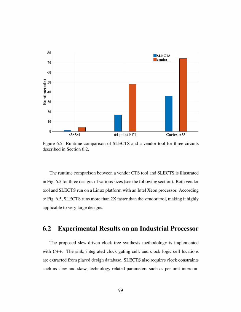
Figure 6.5: Runtime comparison of SLECTS and a vendor tool for three circuitsdescribed in Section 6.2.
The runtime comparison between a vendor CTS tool and SLECTS is illustrated
in Fig. 6.5 for three designs of various sizes (see the following section). Both vendor
tool and SLECTS run on a Linux platform with an Intel Xeon processor. According
to Fig. 6.5, SLECTS runs more than 2X faster than the vendor tool, making it highly
applicable to very large designs.
6.2 Experimental Results on an Industrial Processor
The proposed slew-driven clock tree synthesis methodology is implemented
with C++. The sink, integrated clock gating cell, and clock logic cell locations
are extracted from placed design database. SLECTS also requires clock constraints
such as slew and skew, technology related parameters such as per unit intercon-
99

nect resistance and capacitance, and characterization file (look-up tables) for clock
buffers within the library.
After clock tree synthesis, SLECTS generates two files: 1) a tcl script with the
type and location of clock buffers that are inserted throughout the clock tree, 2) a
SPICE netlist of the clock tree for timing and power analysis based on the provided
timing library and technology related parameters.
SLECTS is evaluated with three circuits of varying sizes ranging from 5K to
over 1M gates (including an industrial processor), as listed in Table 6.1. The
s38584 ISCAS’89 benchmark and 64-point FFT core [106] are implemented in
a 45 nm CMOS technology [107] and operate at 1 GHz clock frequency, whereas
the A53 processor is designed using a 28 nm FDSOI technology [108] and operates
at 1.5 GHz clock frequency. All of the three designs are clock gated and the inte-
grated clock gating cells are inserted automatically by the logic synthesis tool. The
64-point FFT core and Cortex A53 processor clock tree floorplan synthesized by
SLECTS are depicted in Fig. 6.6. These clock trees (the clock buffers and nets ex-
tracted with RC parasitics) and a counterpart synthesized by a commercial vendor
tool are simulated in SPICE. The performance characteristics such as slew, skew,
and number of clock buffers as well as power consumption are compared. The re-
sults are presented under two scenarios for each circuit. The first scenario represents
the slowest corner to evaluate SLECTS under the worst case operating conditions.
The second scenario is the evaluation and comparison under scaled supply voltages.
These results are presented in the following subsections.
100

(a) 64-point FFT core clock tree floorplan.
(b) Cortex A53 processor clock tree floorplan.
Figure 6.6: Illustration of the clock trees synthesized with SLECTS: (a) 64-pointFFT core floorplan, (b) Cortex A53 floorplan.
101
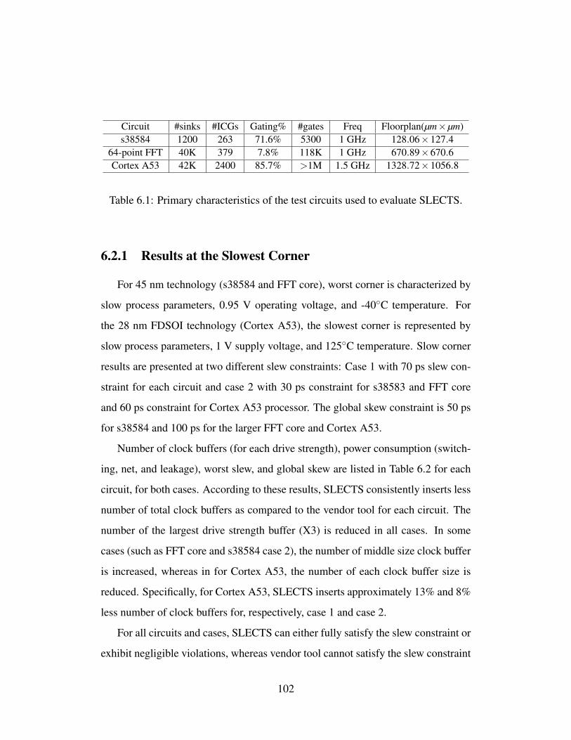
Circuit #sinks #ICGs Gating% #gates Freq Floorplan(µm×µm)s38584 1200 263 71.6% 5300 1 GHz 128.06×127.4
64-point FFT 40K 379 7.8% 118K 1 GHz 670.89×670.6Cortex A53 42K 2400 85.7% >1M 1.5 GHz 1328.72×1056.8
Table 6.1: Primary characteristics of the test circuits used to evaluate SLECTS.
6.2.1 Results at the Slowest Corner
For 45 nm technology (s38584 and FFT core), worst corner is characterized by
slow process parameters, 0.95 V operating voltage, and -40C temperature. For
the 28 nm FDSOI technology (Cortex A53), the slowest corner is represented by
slow process parameters, 1 V supply voltage, and 125C temperature. Slow corner
results are presented at two different slew constraints: Case 1 with 70 ps slew con-
straint for each circuit and case 2 with 30 ps constraint for s38583 and FFT core
and 60 ps constraint for Cortex A53 processor. The global skew constraint is 50 ps
for s38584 and 100 ps for the larger FFT core and Cortex A53.
Number of clock buffers (for each drive strength), power consumption (switch-
ing, net, and leakage), worst slew, and global skew are listed in Table 6.2 for each
circuit, for both cases. According to these results, SLECTS consistently inserts less
number of total clock buffers as compared to the vendor tool for each circuit. The
number of the largest drive strength buffer (X3) is reduced in all cases. In some
cases (such as FFT core and s38584 case 2), the number of middle size clock buffer
is increased, whereas in for Cortex A53, the number of each clock buffer size is
reduced. Specifically, for Cortex A53, SLECTS inserts approximately 13% and 8%
less number of clock buffers for, respectively, case 1 and case 2.
For all circuits and cases, SLECTS can either fully satisfy the slew constraint or
exhibit negligible violations, whereas vendor tool cannot satisfy the slew constraint
102
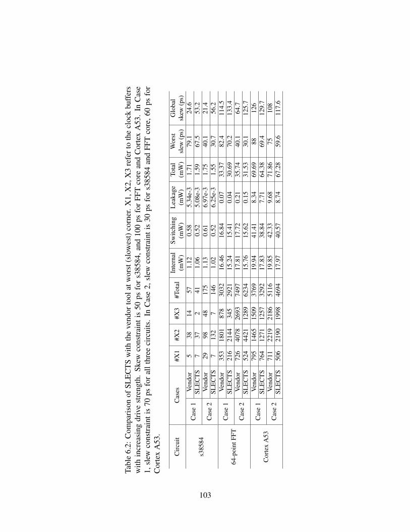
Tabl
e6.
2:C
ompa
riso
nof
SLE
CT
Sw
ithth
eve
ndor
tool
atw
orst
(slo
wes
t)co
rner
.X
1,X
2,X
3re
fert
oth
ecl
ock
buff
ers
with
incr
easi
ngdr
ive
stre
ngth
.Sk
ewco
nstr
aint
is50
psfo
rs3
8584
,and
100
psfo
rFF
Tco
rean
dC
orte
xA
53.
InC
ase
1,sl
ewco
nstr
aint
is70
psfo
ral
lthr
eeci
rcui
ts.
InC
ase
2,sl
ewco
nstr
aint
is30
psfo
rs3
8584
and
FFT
core
,60
psfo
rC
orte
xA
53.
Cir
cuit
Cas
es#X
1#X
2#X
3#T
otal
Inte
rnal
Switc
hing
Lea
kage
Tota
lW
orst
Glo
bal
(mW
)(m
W)
(mW
)(m
W)
slew
(ps)
skew
(ps)
s385
84C
ase
1V
endo
r5
3814
571.
120.
585.
34e-
31.
7179
.124
.6SL
EC
TS
737
241
1.06
0.52
5.08
e-3
1.59
67.5
53.2
Cas
e2
Ven
dor
2998
4817
51.
130.
616.
97e-
31.
7540
.121
.4SL
EC
TS
713
27
146
1.02
0.52
6.25
e-3
1.55
30.7
56.2
64-p
oint
FFT
Cas
e1
Ven
dor
353
1801
878
3032
16.4
616
.84
0.07
33.3
782
.411
4.5
SLE
CT
S21
621
4434
529
2115
.24
15.4
10.
0430
.69
70.2
133.
4
Cas
e2
Ven
dor
726
4078
2693
7497
17.8
117
.72
0.21
35.7
440
.164
.7SL
EC
TS
524
4421
1289
6234
15.7
615
.62
0.15
31.5
330
.112
5.7
Cor
tex
A53
Cas
e1
Ven
dor
795
1465
1509
3769
19.9
441
.41
8.34
69.6
988
126
SLE
CT
S76
412
7112
5732
9217
.83
38.8
47.
7164
.38
69.4
129.
7
Cas
e2
Ven
dor
711
2219
2186
5116
19.8
542
.33
9.68
71.8
675
108
SLE
CT
S50
621
9019
9846
9417
.97
40.5
78.
7467
.28
59.6
117.
6
103

in any of the cases. These results demonstrate the slew-awareness of the proposed
methodology. For example, for Cortex A53, in case 1 (70 ps constraint), the vendor
tool provides a worst slew of 88 ps whereas SLECTS achieves a worst slew of 69
ps. A similar trend is observed for other circuits.
The worst global skew results of s38584 demonstrate that SLECTS uses the
skew budget more effectively by delivering skew results that are closer to the con-
straint of 50 ps (despite slight violations) whereas the vendor tool delivers skew
results significantly lower than the constraint. In the proposed methodology, the ef-
fective use of slew and skew budgets reduces the overall clock power, as discussed
below. For the larger FFT core and Cortex A53 where skew constraint is 100 ps,
both vendor tool and SLECTS exhibit violations, but the delivered worst skew of
the vendor tool is closer to the constraint. This result is intuitive since the existing
methodologies are primarily delay (skew) driven. For example, for Cortex A53,
in case 1, worst skew achieved by the vendor tool and SLECTS are, respectively,
126 ps and 130 ps. In case 2, the worst skews are, respectively, 108 ps and 118
ps. Thus, even though SLECTS exhibits skew violations, the results are still com-
parable to the vendor tool. These skew violations in SLECTS occur due to the
difficulty in producing exact delay values through buffer insertion since the buffer
delay strongly depends upon the load of the node and the interconnect length be-
tween the pairs. For example, if the interconnect length between the pairs is not
sufficiently long, even the smallest size clock buffer does not produce sufficient
delay to fix the insertion delay mismatches.
SLECTS methodology lowers the overall power consumption of the clock tree
in each circuit, as depicted in Fig. 6.7. An average of approximately 9% reduction
in power is achieved. Since slew and skew are simultaneously considered while
104
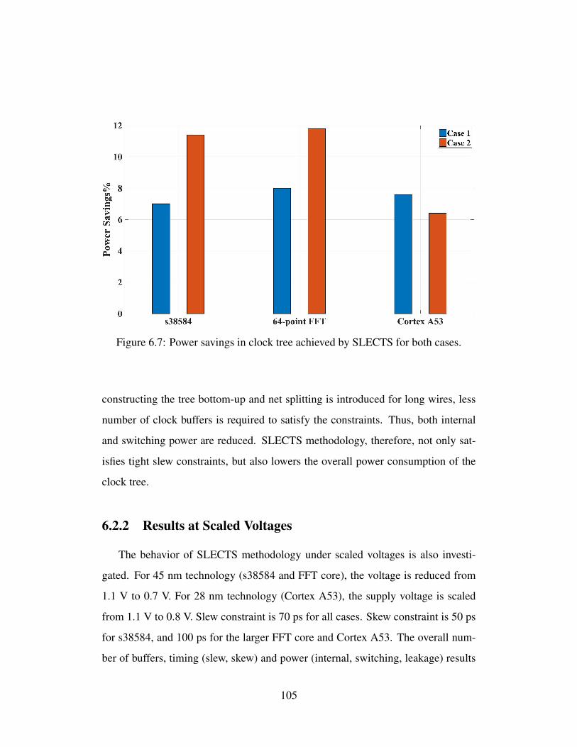
Figure 6.7: Power savings in clock tree achieved by SLECTS for both cases.
constructing the tree bottom-up and net splitting is introduced for long wires, less
number of clock buffers is required to satisfy the constraints. Thus, both internal
and switching power are reduced. SLECTS methodology, therefore, not only sat-
isfies tight slew constraints, but also lowers the overall power consumption of the
clock tree.
6.2.2 Results at Scaled Voltages
The behavior of SLECTS methodology under scaled voltages is also investi-
gated. For 45 nm technology (s38584 and FFT core), the voltage is reduced from
1.1 V to 0.7 V. For 28 nm technology (Cortex A53), the supply voltage is scaled
from 1.1 V to 0.8 V. Slew constraint is 70 ps for all cases. Skew constraint is 50 ps
for s38584, and 100 ps for the larger FFT core and Cortex A53. The overall num-
ber of buffers, timing (slew, skew) and power (internal, switching, leakage) results
105

Tabl
e6.
3:C
ompa
riso
nof
SLE
CT
Sw
ithth
eve
ndor
tool
atsc
aled
supp
lyvo
ltage
s.X
1,X
2,X
3re
fert
oth
ecl
ock
buff
ers
with
incr
easi
ngdr
ive
stre
ngth
.Sk
ewco
nstr
aint
is50
psfo
rs3
8584
,an
d10
0ps
for
FFT
core
and
Cor
tex
A53
.Sl
ewco
nstr
aint
is70
psfo
rall
thre
eci
rcui
ts.
Cir
cuit
Cas
es#X
1#X
2#X
3#T
otal
Inte
rnal
Switc
hing
Lea
kage
Tota
lW
orst
Glo
bal
(mW
)(m
W)
(mW
)(m
W)
slew
(ps)
skew
(ps)
s385
84
1.1V
Ven
dor
245
2673
0.42
30.
577
0.01
61.
016
74.9
48.5
SLE
CT
S5
3722
640.
389
0.52
30.
015
0.92
770
.155
.4
1.0V
Ven
dor
146
3178
0.38
50.
478
0.01
40.
877
77.7
49.6
SLE
CT
S4
4024
680.
359
0.42
10.
011
0.79
169
.861
.5
0.9V
Ven
dor
348
3384
0.29
40.
355
0.01
00.
659
76.9
45.8
SLE
CT
S4
4330
770.
261
0.30
40.
009
0.57
470
.257
.8
0.8V
Ven
dor
552
3693
0.23
80.
291
0.00
70.
536
78.6
47.9
SLE
CT
S3
4336
820.
244
0.24
80.
007
0.49
969
.849
.7
0.7V
Ven
dor
855
3710
00.
187
0.23
10.
004
0.42
279
.946
.2SL
EC
TS
249
3889
0.18
10.
201
0.00
30.
385
70.1
54.1
64-p
oint
FFT
1.1V
Ven
dor
509
1769
1402
3680
16.1
221
.85
0.77
38.7
392
.912
7.5
SLE
CT
S71
217
4789
233
5114
.70
19.8
60.
7235
.28
70.2
117.
8
1.0V
Ven
dor
511
1785
1521
3817
14.5
717
.11
0.53
32.2
191
.711
5.9
SLE
CT
S65
418
3998
134
7412
.59
16.0
70.
501
29.1
669
.912
1.5
0.9V
Ven
dor
487
1950
1673
4110
10.8
814
.32
0.35
25.5
593
.310
5.8
SLE
CT
S66
720
3410
5737
5810
.42
13.0
80.
3023
.80
70.4
109.
3
0.8V
Ven
dor
501
2142
1724
4367
9.03
11.0
80.
2620
.37
95.4
109.
4SL
EC
TS
576
2092
1312
3980
7.64
9.58
0.22
17.4
369
.110
6.8
0.7V
Ven
dor
498
2289
1763
4550
6.62
8.18
0.20
15.0
094
.810
0.7
SLE
CT
S52
120
8915
2341
335.
747.
180.
1713
.10
70.5
105.
1
Cor
tex
A53
1.1V
Ven
dor
636
1185
649
2470
11.3
537
.09
0.17
48.6
196
108
SLE
CT
S75
110
4737
921
779.
5435
.22
0.14
44.9
70.1
111.
5
1.0V
Ven
dor
590
1185
861
2636
9.12
30.5
90.
1239
.83
9113
2SL
EC
TS
458
1102
686
2246
7.24
28.2
10.
135
.55
70.2
124.
3
0.9V
Ven
dor
658
1207
1245
3110
7.81
24.8
20.
0932
.72
9012
3SL
EC
TS
688
1014
1007
2709
6.02
22.7
90.
0728
.88
70.3
125.
7
0.8V
Ven
dor
1019
1656
1588
4236
6.87
19.7
70.
0826
.72
7411
3SL
EC
TS
983
1575
1317
3875
4.9
17.8
60.
0622
.82
70.2
119.
9
106

are listed in Table 6.3 for different voltages. Similar to the worst corner results,
SLECTS consistently inserts less number of buffers for each supply voltage. De-
spite voltage scaling, slew constraint is satisfied, even at the lowest voltages. The
global skew results delivered by SLECTS are closer to the vendor tool as compared
to the worst corner results. For certain cases, such as Cortex A53 at 1 V, SLECTS
achieves a lower global skew (132 ps vs 124 ps). Another interesting observa-
tion for Cortex A53 is that the power savings achieved by SLECTS increase from
approximately 8% to 15% as the voltage is scaled from 1.1 V to 0.8 V. This result
demonstrates the significance of slew driven clock tree synthesis approach for lower
operating voltages.
6.3 SLECTS with the Low Swing Flip-Flop
A novel D flip-flop was proposed in Chapter 3. The proposed flip-flop can reli-
ably operate with a low swing clock signal despite a full swing data signal. Simula-
tion results demonstrate that the proposed topology can achieve similar clock-to-Q
as that of conventional full swing D flip-flop, thereby preventing any performance
degradation in low swing clocking. The power consumption of a conventional full
swing flip-flop and the proposed low swing flip-flop is compared in Fig. 6.8 as a
function of clock swing. As the clock swing is reduced, the power consumption of
the conventional flip-flop significantly increases due to the high short circuit current
dissipated by the clock inverters. Up to 45.5% power is saved at a clock swing of
0.7 V. See Chapter 3 for further cell-level results related to the proposed low swing
flip-flop.
A slew driven clock tree synthesis algorithm referred to as SLECTS was in-
107

Figure 6.8: The comparison of power dissipated by conventional full swing flip-flopand the proposed low swing flip-flop as a function of clock swing.
troduced in this chapter to satisfy the skew and slew constraints in voltage-scaled
clock trees, while dissipating less power. Contrary to existing approaches that are
delay driven, the proposed clock tree synthesis process prioritizes slew over delay
since satisfying the slew constraint is highly challenging in nanoscale technologies
with higher interconnect resistance and low voltage clock trees.
The significant power reduction achieved by the simultaneous application of
the proposed flip-flop and slew aware clock tree synthesis procedure on ISCAS’89
benchmark s38584 and a larger 64-point FFT core is presented in this section. Thus,
the results presented in this section represent a clock tree synthesized by the pro-
posed novel algorithm, driving low swing flip-flops, also proposed in this disserta-
tion.
108

Figure 6.9: The comparison of the clock power of s38584 in two cases: (1) vendortool synthesized clock tree with conventional full swing flip-flops at the nominalvoltage, (2) SLECTS synthesized clock tree with the proposed low swing flip-flopsat different clock swings.
6.3.1 ISCAS’89 Benchmark s38584
ISCAS’89 benchmark s38584 is designed in 45 nm technology and has approx-
imately 1200 flip-flops. The circuit is first synthesized by using conventional full
swing flip-flops and the clock network is synthesized by a vendor tool at the nomi-
nal voltage. The overall clock power (clock network and flip-flops) is determined.
Next, the circuit is synthesized by using the proposed low swing flip-flops and the
clock network is synthesized by the proposed SLECTS methodology, at different
clock swings. The overall clock power in these two cases is compared in Fig. 6.9.
Note that SLECTS synthesized clock tree uses the conventional full swing flip-flop
at 1.1 V clock swing, since the low swing flip-flop consumes 26.5% more power
at this swing, as depicted in Fig. 6.8. For all other clock swings, the proposed flip-
flop is used. At a clock swing of 0.7 V, approximately 52% power is saved (9 mW
109

vs 4.34 mW). Note that the clock power for this circuit is approximately 65.5% of
the overall power consumption. Since the flip-flops consume a significant portion
of the overall clock power, replacing the conventional full-swing flip-flop with the
proposed flip-flop achieves significant power savings.
In Fig. 6.10, the vendor tool synthesized clock tree with conventional flip-flops
is evaluated and compared with the proposed method at different clock swings.
Since the power consumed by the conventional flip-flop increases significantly at
lower clock swings (due to short circuit current), the overall clock power increases
(despite reduction in the power consumed by the clock buffers). In this case, at a
clock swing of 0.7 V, the power savings increase to approximately 67% (12.95 mW
vs 4.34 mW). Replacing all of the conventional flip-flops with the proposed low
swing flip-flop in s38584 design increases the overall area by 32%.
Figure 6.10: The comparison of the clock power of s38584 at different clockswings.
110

6.3.2 64-point FFT Core
64-point FFT core with approximately 40K sinks designed in 45 nm technology
is also evaluated. According to Fig. 6.11, for this larger circuit, approximately
48% power is saved when the proposed low swing flip-flop is used with the clock
tree synthesized by SLECTS methodology at a clock swing of 0.7 V. Specifically,
the overall clock power for the conventional case is 366.86 mW whereas in the
proposed scheme, only 191.9 mW power is consumed. Note that the clock power
for this circuit is approximately 48% of the overall power consumption.
Figure 6.11: The comparison of the clock power of 64-point FFT core in two cases:(1) vendor tool synthesized clock tree with conventional full swing flip-flops at thenominal voltage, (2) SLECTS synthesized clock tree with the proposed low swingflip-flops at different clock swings.
If the clock swing is reduced in the conventional case, as depicted in Fig. 6.12,
the power savings achieved by the proposed scheme increase to approximately 69%
(625.86 mW vs. 191.88 mW) since the power consumed by the conventional flip-
flops increases at lower clock swings. The area overhead due to replacing the flip-
111
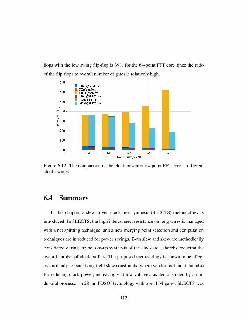
flops with the low swing flip-flop is 39% for the 64-point FFT core since the ratio
of the flip-flops to overall number of gates is relatively high.
Figure 6.12: The comparison of the clock power of 64-point FFT core at differentclock swings.
6.4 Summary
In this chapter, a slew-driven clock tree synthesis (SLECTS) methodology is
introduced. In SLECTS, the high interconnect resistance on long wires is managed
with a net splitting technique, and a new merging point selection and computation
techniques are introduced for power savings. Both slew and skew are methodically
considered during the bottom-up synthesis of the clock tree, thereby reducing the
overall number of clock buffers. The proposed methodology is shown to be effec-
tive not only for satisfying tight slew constraints (where vendor tool fails), but also
for reducing clock power, increasingly at low voltages, as demonstrated by an in-
dustrial processor in 28 nm FDSOI technology with over 1 M gates. SLECTS was
112
integrated into contemporary academic and industrial CTS tool flows for a slew-
driven approach, similar to DME that is popular for the traditional skew-driven
CTS approaches. The power analysis of combining SLECTS and low swing flip-
flop demonstrates significant power savings without performance degradation.
113

Chapter 7
Conclusion and Future Directions
Low swing clocking is an effective technique to reduce clock network power
dissipation. However, existing works on low swing/voltage clock networks are ef-
fective primarily for low power applications that do not demand high performance.
In this thesis, a novel static D-type flip-flop design, a level shifter for selective
low swing clocking, a clock skew scheduling methodology with two different ob-
jectives and a slew-driven clock tree synthesis algorithm are proposed to facilitate
low swing operation without degrading circuit performance. These contributions
are summarized in Section 7.1. Several possible future directions are discussed in
Section 7.2.
7.1 Thesis Summary
As technology scales and die area increases, designing a voltage-scaled clock
network operating at the same performance has become challenging. Traditional
flip-flops cannot reliably work with a reduced swing clock signal. Thus, level
114
shifters are typically inserted at the sinks to restore clock signal to full swing. How-
ever, this approach limits the overall power savings since the last stage of a clock
network typically has the largest capacitance and therefore benefits the most from
low swing clocking. A novel D flip-flop is proposed in Chapter 3. The proposed
flip-flop can reliably operate with a low swing clock signal. Simulation results
demonstrate that the proposed topology can achieve similar clock-to-Q as that of
conventional full swing D flip-flop, preventing any performance degradation in low
swing clocking while maximizing power savings.
In high performance clock trees with sufficiently low skew and slew require-
ment, it may not be practical to lower the clock voltage of the entire clock tree.
Selective low voltage clocking has been considered for such situations where part
of the clock tree operates at a reduced voltage (to save power) and the rest of the tree
operates at nominal voltage to satisfy the performance constraints. Thus, a low over-
head level shifter is required to restore clock voltage level. A novel level-up shifter
with dual supply voltage is proposed to enable selective low voltage clocking, as
described in Chapter 4. The proposed level shifter is compared with conventional
cross-coupled topology and level shifters with bootstrapping technique. Simulation
results demonstrate the superior performance of the proposed level shifter.
Clock gating is an effective technique to reduce clock network dynamic power
dissipation. Thus, modern ICs are typically clock-gated. Existing clock skew
scheduling methods cannot effectively consider clock gating when an ICG cell gates
multiple registers. In such case, a local clock tree typically exists between the ICG
cell and registers gated by this ICG cell, introducing additional and unbalanced
clock propagation paths. Furthermore, the Enable timing paths of the clock gating
cells introduce challenges on satisfying circuit timing constraint, particularly for
115
low swing clock networks. Therefore, a clock skew scheduling algorithm is pro-
posed in Chapter 5 to maximize circuit performance and increase the timing slack
of Enable paths. The largest ISCAS’89 benchmark circuits are used to evaluate
the proposed algorithm. Simulation results demonstrate that the proposed algo-
rithm can improve circuit performance and facilitate low swing clocking in gated
designs.
A slew driven clock tree synthesis algorithm, referred to as SLECTS, is pro-
posed in Chapter 6 to simultaneously satisfy the skew and slew constraints in 1)
nanoscale technologies with high interconnect resistance and 2) voltage-scaled clock
networks. Contrary to existing approaches that are delay driven, the proposed clock
tree synthesis process prioritizes slew over delay since satisfying the slew constraint
is highly challenging in low voltage clock trees. The proposed algorithm is eval-
uated on a large industrial circuit with more than one million gates. Simulation
results demonstrate that the proposed algorithm satisfies the slew constraint while
reducing the overall clocking power as compared to a vendor tool. The simul-
taneous application of the proposed flip-flop and slew aware clock tree synthesis
procedure demonstrates significant power reduction on an industrial processor.
7.2 Future Directions
In nanoscale technologies, on-chip variation (OCV) has become a challenging
problem, particularly for timing closure. Single derating factor based methods have
been recently replaced by more advanced and accurate OCV and parametric OCV
tables. Since clock networks typically drive a large number of sinks/flip-flops that
are distributed throughout the entire die, clock nets run across multiple domains
116

operating with different process-voltage-temperature corners. Thus, clock tree cells
significantly suffer from the effects of OCV. Future work on clock tree synthesis can
focus on developing a variation-aware clock tree while still satisfying the slew and
skew constraints. Clock network insertion delay can be better controlled to mini-
mize the effects of variations. More importantly, these variations can be considered
(by utilizing the parametric OCV tables) during the synthesis process to develop a
clock tree that is correct by design.
Voltage scaled clock networks suffer from lower noise tolerance. Thus, another
important future direction is to evaluate and quantify the effect of low clock voltage
on the robustness of the clock tree. This evaluation can be achieved through static
noise analysis approaches, similar to static timing analysis that is critical for per-
formance verification. In the next step, clock buffer sizes and interconnect widths
can be determined to maximize noise tolerance while still considering clock skew
and slew. Thus, similar to variation-awareness, the noise-awareness can also be
integrated into the synthesis process.
117

Bibliography
[1] J. Zhang and Y. Sun, “A low clock swing, power saving and generic technol-
ogy based d flip-flop with single power supply,” in ASIC, 2007. ASICON’07.
7th International Conference on. IEEE, 2007, pp. 142–144.
[2] H. Kawaguchi and T. Sakurai, “A reduced clock-swing flip-flop (rcsff) for
63% power reduction,” Solid-State Circuits, IEEE Journal of, vol. 33, no. 5,
pp. 807–811, 1998.
[3] M. Tokumasu, H. Fujii, M. Ohta, T. Fuse, and A. Kameyama, “A new re-
duced clock-swing flip-flop: Nand-type keeper flip-flop (ndkff),” in Custom
Integrated Circuits Conference, 2002. Proceedings of the IEEE 2002. IEEE,
2002, pp. 129–132.
[4] D. Levacq, M. Yazid, H. Kawaguchi, M. Takamiya, and T. Sakur, “Half v dd
clock-swing flip-flop with reduced contention for up to 60% power saving in
clock distribution,” in Solid State Circuits Conference, 2007. ESSCIRC 2007.
33rd European. IEEE, 2007, pp. 190–193.
[5] E. Salman and E. G. Friedman, High Performance Integrated Circuit Design.
McGraw-Hill, 2012.
118

[6] F. Chang et al., “Practical strategies for power-efficient computing technolo-
gies,” Proceedings of the IEEE, vol. 98, no. 2, pp. 215–236, 2010.
[7] D. Liu and C. Svensson, “Power consumption estimation in cmos vlsi chips,”
Solid-State Circuits, IEEE Journal of, vol. 29, no. 6, pp. 663–670, 1994.
[8] P. Pillai and K. G. Shin, “Real-time dynamic voltage scaling for low-power
embedded operating systems,” in ACM SIGOPS Operating Systems Review,
vol. 35, no. 5. ACM, 2001, pp. 89–102.
[9] T. Pering, T. Burd, and R. Brodersen, “The simulation and evaluation of
dynamic voltage scaling algorithms,” in Low Power Electronics and Design,
1998. Proceedings. 1998 International Symposium on. IEEE, 1998, pp.
76–81.
[10] R. Gonzalez, B. M. Gordon, M. Horowitz et al., “Supply and threshold volt-
age scaling for low power cmos,” Solid-State Circuits, IEEE Journal of,
vol. 32, no. 8, pp. 1210–1216, 1997.
[11] E. G. Friedman, “Clock distribution networks in synchronous digital inte-
grated circuits,” Proceedings of the IEEE, vol. 89, no. 5, pp. 665–692, 2001.
[12] H. Kawaguchi and T. Sakurai, “A reduced clock-swing flip-flop (rcsff) for
63% power reduction,” IEEE Journal of Solid-State Circuits, vol. 33, no. 5,
pp. 807–811, 1998.
[13] D. W. Dobberpuhl, R. T. Witek, R. Allmon, R. Anglin, D. Bertucci, S. Brit-
ton, L. Chao, R. A. Conrad, D. E. Dever, B. Gieseke et al., “A 200-mhz
64-b dual-issue cmos microprocessor,” IEEE Journal of Solid-State Circuits,
vol. 27, no. 11, pp. 1555–1567, 1992.
119

[14] K. Chulwoo and K. Sung-Mo, “A low-swing clock double-edge triggered
flip-flop,” Solid-State Circuits, IEEE Journal of, vol. 37, no. 5, pp. 648–652,
2002.
[15] Q. Wu, M. Pedram, and X. Wu, “Clock-gating and its application to low
power design of sequential circuits,” IEEE Transactions on Circuits and
Systems-I: Fundamental Theory and Applications, vol. 47, no. 103, pp. 415–
420, March 2000.
[16] M. Donno, A. Ivaldi, L. Benini, and E. Macii, “Clock-tree power optimiza-
tion based on rtl clock-gating,” in Design Automation Conference, June 2003,
pp. 622–627.
[17] J. Kathuria, M. Ayoubkhan, and A. Noor, “A review of clock gating tech-
niques,” MIT International Journal of Electronics and Communication En-
gineering, vol. 1, no. 2, pp. 106–114, 2011.
[18] H. Mahmoodi, V. Tirumalashetty, M. Cooke, and K. Roy, “Ultra low-power
clocking scheme using energy recovery and clock gating,” IEEE transactions
on very large scale integration (VLSI) systems, vol. 17, no. 1, pp. 33–44,
2009.
[19] R. Gonzalez, B. M. Gordon, and M. A. Horowitz, “Supply and Threshold
Voltage Scaling for Low Power CMOS,” IEEE Journal of Solid-State Cir-
cuits, vol. 32, no. 8, pp. 1210–1216, August 1997.
[20] J.-M. Chang and M. Pedram, “Energy minimization using multiple supply
voltages,” IEEE Transactions on Very Large Scale Integration (VLSI) Sys-
tems, vol. 5, no. 4, pp. 436–443, 1997.
120

[21] B. H. Calhoun and A. P. Chandrakasan, “A 256-kb 65-nm sub-threshold sram
design for ultra-low-voltage operation,” IEEE Journal of Solid-State Circuits,
vol. 42, no. 3, pp. 680–688, 2007.
[22] R. Dreslinski, M. Wieckowski, D. Blaauw, D. Sylvester, and T. Mudge,
“Near-Threshold Computing: Reclaiming Moore’s Law Through Energy Ef-
ficient Integrated Circuits,” Proceedings of the IEEE, vol. 98, no. 2, pp. 253–
266, 2010.
[23] H. Zhang, G. Varghese, and J. M. Rabaey, “Low-swing on-chip signaling
techniques: Effectiveness and robustness,” IEEE Transactions on Very Large
Scale Integration (VLSI) Systems, vol. 8, no. 3, pp. 264–272, June 2000.
[24] J. Pangjun and S. Sapatnekar, “Low-power clock distribution using multi-
ple voltages and reduced swings,” IEEE Transactions on Very Large Scale
Integration (VLSI) Systems, vol. 10, no. 3, pp. 309–318, 2002.
[25] F. H. A. Asgari and M. Sachdev, “A low-power reduced swing global
clocking methodology,” IEEE Transactions on Very Large Scale Integration
(VLSI) Systems, vol. 12, no. 5, pp. 538–545, May 2004.
[26] C. Sitik and B. Taskin, “Skew-bounded low swing clock tree optimization,”
in Proceedings of ACM Great Lakes Symposium on VLSI (GLSVLSI), May
2013, pp. 49–54.
[27] J. R. Tolbert, X. Zhao, S. K. Lim, and S. Mukhopadhyay, “Analysis and de-
sign of energy and slew aware subthreshold clock systems,” IEEE Transac-
tions on Computer-Aided Design of Integrated Circuits and Systems, vol. 30,
no. 9, pp. 1349–1358, September 2011.
121

[28] M. Seok, D. Blaauw, and D. Sylvester, “Clock Network Design for Ultra-
Low Power Applications,” in Proceedings of the ACM/IEEE International
Symposium on Low-Power Electronics and Design, August 2010, pp. 271–
276.
[29] X. Zhao, J. R. Tolbert, C. Liu, S. Mukhopadhyay, and S. K. Lim, “Variation-
Aware Clock Network Design Methodology for Ultra-Low Voltage (ULV)
Circuits,” in Proceedings of the ACM/IEEE International Symposium on
Low-Power Electronics and Design, August 2011, pp. 9–14.
[30] A. F. Champernowne, L. B. Bushard, J. T. Rusterholz, and J. R. Schomburg,
“Latch-to-latch timing rules,” Computers, IEEE Transactions on, vol. 39,
no. 6, pp. 798–808, 1990.
[31] P. J. Restle and A. Deutsch, “Designing the best clock distribution network,”
in VLSI Circuits, 1998. Digest of Technical Papers. 1998 Symposium on.
IEEE, 1998, pp. 2–5.
[32] S. Pullela, N. Menezes, J. Omar, and L. T. Pillage, “Skew and delay opti-
mization for reliable buffered clock trees,” in Computer-Aided Design, 1993.
ICCAD-93. Digest of Technical Papers., 1993 IEEE/ACM International Con-
ference on. IEEE, 1993, pp. 556–562.
[33] E. G. Friedman and S. Powell, “Design and analysis of a hierarchical clock
distribution system for synchronous standard cell/macrocell vlsi,” Solid-State
Circuits, IEEE Journal of, vol. 21, no. 2, pp. 240–246, 1986.
[34] D. Mijuskovic, “Clock distribution in application specific integrated cir-
cuits,” Microelectronics Journal, vol. 18, no. 4, pp. 15–27, 1987.
122

[35] H. B. Bakoglu, “Circuits, interconnections, and packaging for vlsi.” 1990.
[36] J. Rosenfeld and E. G. Friedman, “Design methodology for global resonant
h-tree clock distribution networks,” IEEE Transactions on Very Large Scale
Integration (VLSI) Systems, vol. 15, no. 2, pp. 135–148, 2007.
[37] T. Xanthopoulos, D. W. Bailey, A. K. Gangwar, M. K. Gowan, A. K. Jain,
and B. K. Prewitt, “The design and analysis of the clock distribution net-
work for a 1.2 ghz alpha microprocessor,” in Solid-State Circuits Conference,
2001. Digest of Technical Papers. ISSCC. 2001 IEEE International. IEEE,
2001, pp. 402–403.
[38] V. F. Pavlidis, I. Savidis, and E. G. Friedman, “Clock distribution networks
for 3-d ictegrated circuits,” in Custom Integrated Circuits Conference, 2008.
CICC 2008. IEEE. IEEE, 2008, pp. 651–654.
[39] N. H. Weste and D. Harris, CMOS VLSI design: a circuits and systems per-
spective. Pearson Education India, 2015.
[40] N. H. Weste and K. Eshraghian, Principles of CMOS VLSI design. Addison-
Wesley New York, 1985, vol. 188.
[41] L.-T. Wang, Y.-W. Chang, and K.-T. T. Cheng, Electronic design automation:
synthesis, verification, and test. Morgan Kaufmann, 2009.
[42] J. Burkis, “Clock tree synthesis for high performance asics,” in ASIC Con-
ference and Exhibit, 1991. Proceedings., Fourth Annual IEEE International.
IEEE, 1991, pp. P9–8.
123

[43] K. D. Boese and A. B. Kahng, “Zero-skew clock routing trees with minimum
wirelength,” in ASIC Conference and Exhibit, 1992., Proceedings of Fifth
Annual IEEE International. IEEE, 1992, pp. 17–21.
[44] R.-S. Tsay, “An exact zero-skew clock routing algorithm,” Computer-Aided
Design of Integrated Circuits and Systems, IEEE Transactions on, vol. 12,
no. 2, pp. 242–249, 1993.
[45] Y.-C. Hsu, J.-M. Ho, and A. Kahng, “Zero skew clock routing with minimum
wirelength,” Circuits and Systems II: Analog and Digital Signal Processing,
IEEE Transactions on, vol. 39, no. 11, pp. 799–814, 1992.
[46] J. Cong and C.-K. Koh, “Minimum-cost bounded-skew clock routing,” in
Circuits and Systems, 1995. ISCAS’95., 1995 IEEE International Symposium
on, vol. 1. IEEE, 1995, pp. 215–218.
[47] J. Cong, A. B. Kahng, C.-K. Koh, and C.-W. A. Tsao, “Bounded-skew clock
and steiner routing,” ACM Transactions on Design Automation of Electronic
Systems (TODAES), vol. 3, no. 3, pp. 341–388, 1998.
[48] J. G. Xi and W. W.-M. Dai, “Useful-skew clock routing with gate sizing
for low power design,” in High Performance Clock Distribution Networks.
Springer, 1997, pp. 51–67.
[49] C.-W. A. Tsao and C.-K. Koh, “Ust/dme: a clock tree router for general skew
constraints,” ACM Transactions on Design Automation of Electronic Systems
(TODAES), vol. 7, no. 3, pp. 359–379, 2002.
124

[50] C. Sitik, W. Liu, B. Taskin, and E. Salman, “Design methodology for voltage-
scaled clock distribution networks,” IEEE Transactions on Very Large Scale
Integration (VLSI) Systems, vol. 24, no. 10, pp. 3080–3093, 2016.
[51] M. Rathore, W. Liu, E. Salman, C. Sitik, and B. Taskin, “A Novel Static
D-Flip-Flop Topology for Low Swing Clocking,” in Proceedings of the
ACM/IEEE Great Lakes Symposium on VLSI, May 2015, pp. 301–306.
[52] W. Liu, E. Salman, C. Sitik, B. Taskin, S. Sundareswaran, and B. Huang,
“Circuits and algorithms to facilitate low swing clocking in nanoscale tech-
nologies,” in Proceedings of Semiconductor Research Corporation (SRC)
TECHCON. SRC, September 2015.
[53] W. Liu, E. Salman, C. Sitik, B. Taskin, S. Sundareswaran, and B. Huang,
“Slew-driven clock tree synthesis (slects) methodology to facilitate low
voltage clocking,” in Proceedings of Semiconductor Research Corporation
(SRC) TECHCON. SRC, September 2016.
[54] W. Liu, E. Salman, A. C. Sitik, and B. Taskin, “Slew-driven clock tree
synthesis,” Patent 20 170 357 286, December, 2017. [Online]. Available:
http://www.freepatentsonline.com/y2017/0357286.html
[55] C. Sitik, E. Salman, L. Filippini, S. J. Yoon, and B. Taskin, “Finfet-based
low-swing clocking,” J. Emerg. Technol. Comput. Syst., vol. 12, no. 2, pp.
13:1–13:20, Sep. 2015.
[56] C. Sitik, L. Filippini, E. Salman, and B. Taskin, “High Performance Low
Swing Clock Tree Synthesis with Custom D Flip-Flop Design,” in Proceed-
125

ings of the IEEE Computer Society Annual Symposium on VLSI, July 2014,
pp. 498–503.
[57] W. Liu, E. Salman, C. Sitik, and B. Taskin, “Clock skew scheduling in the
presence of heavily gated clock networks,” in Proceedings of the 25th edition
on Great Lakes Symposium on VLSI. ACM, 2015, pp. 283–288.
[58] W. Liu, E. Salman, C. Sitik, and B. Taskin, “Exploiting useful skew in gated
low voltage clock trees,” in Circuits and Systems (ISCAS), 2016 IEEE Inter-
national Symposium on. IEEE, 2016, pp. 2595–2598.
[59] W. Liu, E. Salman, C. Sitik, and B. Taskin, “Enhanced Level Shifter for
Multi-Voltage Operation,” in Proceedings of the IEEE International Sympo-
sium on Circuits and Systems, May 2015, pp. 1442–1445.
[60] H. Mahmoodi-Meimand and K. Roy, “Dual-edge triggered level converting
flip-flops,” in Proceedings of the IEEE International Symposium on Circuits
and Systems, May 2004, pp. 661–664.
[61] Cadence. Spectre. https://www.cadence.com.
[62] E. Salman, A. Dasdan, F. Taraporevala, K. Kucukcakar and E. G. Friedman,
“Exploiting setup-hold time interdependence in static timing analysis,” IEEE
Transactions on Computer-Aided Design of Integrated Circuits and Systems,
vol. 26, no. 6, pp. 1114–1125, June 2007.
[63] A. Dasdan and I. Hom, “Handling inverted temperature dependence in static
timing analysis,” ACM Transactions on Design Automation of Electronic Sys-
tems, vol. 11, no. 2, pp. 306–324, April 2006.
126
[64] K.-H. Koo, J.-H. Seo, M.-L. Ko, and J.-W. Kim, “A new level-up shifter for
high speed and wide range interface in ultra deep sub-micron,” in IEEE In-
ternational Symposium on Circuits and Systems, may 2005, pp. 1063–1065.
[65] S.-C. Luo, C.-J. Huang, and Y.-H. Chu, “A wide-range level shifter using a
modified wilson current mirror hybrid buffer,” IEEE Transactions on Circuits
and Systems: Regular Papers, vol. 61, no. 6, pp. 1656–1665, jun 2014.
[66] M.-D. Chen and N.-P. Tu, “Cmos digital level shifter circuit,” December
1990, uS Patent 4,978,870.
[67] L. R. Avery and P. D. Gardner, “Crisscross voltage level shifter,” December
1999, uS Patent 6,002,290.
[68] S. Tan and X. Sun, “Low power cmos level shifter by bootstrapping tech-
nique,” Electronics Letters, vol. 38, no. 16, pp. 876–878, aug 2002.
[69] J. Garcia, J. Montiel-Nelson, and S. Nooshabadi, “High performance boot-
strapped cmos dual supply level shifter for 0.5v input and 1v output,” in 18th
European Conference on Circuit Theory and Design, aug 2007, pp. 795–798.
[70] S. Wooters, B. CalHoun, and T. Blalock, “An energy-efficient subthreshold
level converter in 130-nm cmos,” IEEE Transactions on Circuits and Systems
II: Express Briefs, vol. 57, no. 4, pp. 290–294, apr 2010.
[71] S. Lutkemeier and U. Ruckert, “A subthreshold to above-threshold level
shifter comprising a wilson current mirror,” IEEE Transactions on Circuits
and Systems II: Express Briefs, vol. 57, no. 9, pp. 721–724, 2010.
127

[72] Q. Khan, S. Wadhwa, and K. Misri, “A single supply level shifter for multi-
voltage systems,” in Proceedings of the 19th International Conference on
VLSI Design, jan 2006, pp. 557–560.
[73] D.-I. Jeon, K.-S. Han, and K.-S. Chung, “Novel level-up shifters for high
performance and low power mobile devices,” in 2013 IEEE Internatioanl
Conference on Consumer Electronics, jan 2013, pp. 181–182.
[74] J. Shinde and S. Salankar, “Clock gatinga power optimizing technique for
vlsi circuits,” in India Conference (INDICON), 2011 Annual IEEE. IEEE,
2011, pp. 1–4.
[75] V. Tiwari, D. Singh, S. Rajgopal, G. Mehta, R. Patel, and F. Baez, “Reduc-
ing power in high-performance microprocessors,” in Proceedings of the 35th
annual Design Automation Conference. ACM, 1998, pp. 732–737.
[76] J. P. Fishburn, “Clock skew optimization,” IEEE Transactions on Computers,
vol. 39, no. 7, pp. 945–951, July 1990.
[77] T.G.Szymanski, “Computing optimal clock schedules,” in ACM/IEEE De-
sign Automation Conference, June 1992, pp. 399–404.
[78] N.Shenoy, R.K.Brayton, and A.L.Sangiovanni-Vincentelli, “Graph algo-
rithms for clock skew optimization,” in International Conference on
Computer-Aided Design, November 1992, pp. 132–136.
[79] R. Deokar and S. Sapatnekar, “A graph-theoretic approach to clock skew
optimization,” in Int. Symp. on Circuits and Systems, May 1994, pp. 407–
410.
128
[80] B. Taskin and I. S. Kourtev, “Delay insertion method in clock skew schedul-
ing,” IEEE Transactions on Computer-Aided Design of Integrated Circuits
and Systems, vol. 25, no. 4, pp. 651–663, April 2006.
[81] S.-H. Huang, C.-H. Cheng, C.-M. Chang, and Y.-T. Nieh, “Clock period min-
imization with minimum delay insertion,” in Design Automation Conference,
June 2007, pp. 970–975.
[82] K. Ravindran, A. Kuehlmann, and E. Sentovich, “Multi-domain clock
skew scheduling,” in International Conference on Computer-Aided Design,
November 2003, pp. 801–808.
[83] M. Ni and S. O. Memik, “A fast heuristic algorithm for multidomain clock
skew scheduling,” IEEE Transactions on Very Large Scale Integration (VLSI)
Systems, vol. 18, no. 4, pp. 630–637, April 2010.
[84] L. Li, Y. Lu, and H. Zhou, “Optimal and efficient algorithms for multidomain
clock skew scheduling,” IEEE Trans. on Very Large Scale Integration (VLSI)
Systems, vol. 22, no. 9, pp. 1888–1897, Sept. 2014.
[85] T. H. Cormen, C. E. Leiserson, R. L. Rivest, and C. Stein, Introduction to
Algorithms. The MIT Press, 2001.
[86] W.-P. Tu, S.-H. Huang, and C.-H. Cheng, “Co-synthesis of data paths and
clock control paths for minimum-period clock gating,” in Design, Automa-
tion And Test in Europe Conference And Exhibition (DATE), March 2013,
pp. 1831–1836.
[87] Synopsys. Design compiler. http://www.synopsys.com.
129

[88] NanGate. 45nm open cell library. http://www.nangate.com.
[89] GNU. Gnu linear programming kit. https://www.gnu.org/software/glpk/.
[90] S. Tam, “Modern clock distribution systems,” in Clocking in Modern VLSI
Systems. Springer, 2009, pp. 9–65.
[91] N. Kurd and et al., “A multigigahertz clocking scheme for the Pentium 4 mi-
croprocessor,” IEEE Journal of Solid-State Circuits (JSSC), vol. 36, no. 11,
pp. 1647–1653, Nov. 2001.
[92] D. J. Lee, M. C. Kim, and I. Markov, “Low-power clock trees for CPUs,”
in Proceedings of IEEE/ACM International Conference on Computer-Aided
Design (ICCAD), Nov. 2010, pp. 444–451.
[93] M. Edahiro, “A clustering-based optimization algorithm in zero-skew rout-
ings,” in ACM/IEEE Design Automation Conference (DAC), June 1993, pp.
612–616.
[94] R. Chaturvedi and J. Hu, “An efficient merging scheme for prescribed skew
clock routing,” IEEE Transactions on Very Large Scale Integration (TVLSI)
Systems, vol. 13, no. 6, pp. 750–754, Jun 2005.
[95] Y. Cai, C. Deng, Q. Zhou, H. Yao, F. Niu, and C. Sze, “Obstacle-avoiding and
slew-constrained clock tree synthesis with efficient buffer insertion,” IEEE
Transactions on Very Large Scale Integration (TVLSI) Systems, vol. 23, no. 1,
pp. 142–155, Jan. 2014.
130

[96] J. Lu, W.-K. Chow, and C.-W. Sham, “Fast power- and slew-aware gated
clock tree synthesis,” IEEE Transactions on Very Large Scale Integra-
tion (TVLSI) Systems, vol. 20, no. 11, pp. 2094–2103, Nov. 2012.
[97] P. J. Restle, T. G. McNamara, D. A. Webber, P. J. Camporese, K. F. Eng,
K. A. Jenkins, D. H. Allen, M. J. Rohn, M. P. Quaranta, D. W. Boerstler
et al., “A clock distribution network for microprocessors,” IEEE Journal of
Solid-State Circuits, vol. 36, no. 5, pp. 792–799, 2001.
[98] C.-K. Koh, J. Jain, and S. F. Cauley, “Synthesis of clock and power/ground
networks,” Electronic Design Automation: Synthesis, Verification, and Test,
pp. 751–850, 2009.
[99] A. Vittal and M. Marek-Sadowska, “Low-power buffered clock tree design,”
IEEE Transactions on Computer-Aided Design of Integrated Circuits and
Systems, vol. 16, no. 9, pp. 965–975, 1997.
[100] M. M.-S. A. Vittal, “Power optimal buffered clock tree design,” in Design
Automation, 1995. DAC’95. 32nd Conference on. IEEE, 1995, pp. 497–
502.
[101] J. Qian, S. Pullela, and L. Pillage, “Modeling the effective capacitance for
the rc interconnect of cmos gates,” pp. 1526–1535, 1994.
[102] I. S. Kourtev and E. G. Friedman, “Clock skew scheduling for improved reli-
ability via quadratic programming,” in IEEE/ACM International Conference
on Computer-Aided Design, Nov 1999, pp. 239–243.
[103] C. Kashyap, C. Alpert, F. Liu, and A. Devgan, “Closed-form expressions for
extending step delay and slew metrics to ramp inputs for RC trees,” IEEE
131
Transactions on Computer-Aided Design (TCAD) of Integrated Circuits and
Systems, vol. 23, no. 4, pp. 509–516, April 2004.
[104] W. C. Elmore, “The transient response of damped linear networks with par-
ticular regard to wideband amplifiers,” Journal of Applied Physics, vol. 19,
no. 1, pp. 55–63, 1948.
[105] J. Hartigan and M. Wong, “A k-means clustering algorithm,” Journal of the
Royal Statistical Society. Series C, vol. 28, no. 1, pp. 100–108, 1979.
[106] P. Milder, F. Franchetti, J. C. Hoe, and M. Puschel, “Computer generation of
hardware for linear digital signal processing transforms,” ACM Trans. Des.
Autom. Electron. Syst., vol. 17, no. 2, pp. 15:1–15:33, Apr. 2012.
[107] FreePDK 45nm Library v1.4, NCSU, 2011.
[108] 28nm FDSOI Technology Node, TSMC.
132