lecture 26 - university of waterlooleung.uwaterloo.ca/mns/102/lect_2013/lect_26a.pdf · lecture 26...
TRANSCRIPT

Lecture 26 MNS 102: Techniques for Materials and Nano Sciences
• Tip-based Microscopy – History
• Scanning Tunnelling Microscopy (STM): QM tunnelling; basic principle; instrumentation; modes of operation; pros and cons; applications
• Atomic Force Microscopy (AFM): Atomic forces; principle; modes of operation; static vs dynamic modes; applications
• STM vs AFM
1 26-
Reference: #1 C. R. Brundle, C. A. Evans, S. Wilson, "Encyclopedia of Materials Characterization", Butterworth-Heinemann, Toronto (1992), Ch. 2, Ch. 3. References: http://www.veeco.com/pdfs/library/SPM_Guide_0829_05_166.pdf http://www.chembio.uoguelph.ca/educmat/chm729/STMpage/stmtutor.htm http://www.almaden.ibm.com/vis/stm/blue.html http://virtual.itg.uiuc.edu/training/AFM_tutorial/

History
• 1982 Phys. Rev. Lett. 49, 57 - Heinrich Rohrer and Gerd Binnig, IBM Zurich - first discussed the concept of STM.
• 1986 Nobel Prize in Physics.
• 1986 Phys. Rev. Lett. 56, 930 - Binnig, Calvin Quate (Stanford), Christoph Gerber (Basel) invented AFM.
• SPM is often considered a main driver for nanotechnology.
26- 2

Quantum Mechanical Tunnelling
• One-dimensional electron tunnelling through a rectangular barrier – Start with the particle-in-a-double-box case and lower the barrier between the two boxes…
• Elastic vs inelastic tunnelling: Elastic tunnelling – energy of tunnelling electron is conserved; Inelastic tunnelling – electron loses a quantum of energy inside the tunnelling barrier.
• Electron tunnelling in STM:
26- 3

STM: Basic Principle
• “Move” the tip so close to the sample that their wavefunctions begin to overlap and to enable quantum mechanical tunnelling;
• Apply a bias voltage to the tip to “facilitate” electron transport (i.e. tunnelling);
• Positive sample bias: Tunnelling from tip (filled state near the Fermi energy) to the empty states of the sample – Empty state imaging;
• Negative sample bias: Tunnelling from sample (filled states near the Fermi energy of the sample) to empty states of the tip – Filled-state imaging.
26- 4
Thermal equilibrium - Zero Bias Positive Sample Bias Negative Sample Bias

Filled-state vs Empty-state Imaging
26- 5
Ref: J. J. Boland, Adv. Phys. 42 (1993) 129.

Tunnelling Current
26- 6
• Quantum Mechanics predicts that the wavefunction decays exponentially through the barrier:
• Probability of finding the electron after the barrier of width d is:
• The current is: I = f(V) e-2Kd where f(V) is a function that contains a weighted joint local density of states (LDOS) that reflects the property of the material.
• The tunnelling current is therefore: I e-2Kd where K (2m ) / (h/2) = 0.51 Å-1 and is the work function (in eV). When 4 eV, K 1 Å-1 and e2 7.4 . This means tunnelling current goes down by 7.4 times per Å. (In the 2nd tip, two atoms away from the atom in the first tip. This means that the second tip will detect ~106 less current than the first tip. Extreme z sensitivity!)
• Note that the tunnelling current does not reflect the nuclear position directly. STM measures the local electron density of states and not nuclear position.

Instrumentation
• Anti-vibration: 1 Hz – general human movement; 10-100 Hz – electronics, ventilation; Target 1-10 kHz resonant frequency for STMs
• Building vibration 1 m will generate 1 pm at the STM tip
• Make STM system as rigid as possible so that internal resonance is above 1 kHz and mount it on a low resonant frequent support
• Coarse approach: Move tip up and down from mm to sub-m; use beetle-type motion and inertial slider; base materials must undergo similar thermal expansion of piezoelectric tube (the scanner), mechanically rigid – macor is used b/c stiff and lightweight
26- 7

Fine Approach: Piezoelectric Scanner
• Piezoelectric material is a “smart” material that changes in dimension under an applied voltage.
• Piezoelectric scanner must have high resonance frequencies and scan speed, high sensitivity, low crosstalk among x, y, z drivers, and low thermal drift.
26- 8
Tube scanner: 15 mm long, 5 mm dia, 0.75 mm thick can provide motions up to 1.0 m vertically and 2.8 m laterally.
Omicron VT STM tip setup with tip coming from below, and sample facing down.

Piezoelectric Materials
• Piezoelectric materials produce a voltage in response to an applied force, i.e. Displacement electric field
• Piezoelectric materials have an asymmetric unit cell like a dipole. E.g. PZT = lead zirco-nium titanate (250-365x10-12m/V); barium titanate (100-149x10-12m/V); lead niobate (80-85x10-12m/V); quartz (2.3x10⁻¹²m/V).
• Issues: Nonlinearity; creep; hysteresis; aging – Keep the Voltage low when not in use.
26- 9
Uh
ldZ 0
Barium titanate - replace Pb with Ba in the tetragonal perovskite structure.

Modes of Operation for Imaging
• Constant height mode: Measure I(x,y) at a fixed height z (with feedback off) – This corresponds to variation of the Density of States (DOS) at fixed height. Usually high contrast and fast scanning, insensitive to low-frequency mechanical vibrations and electronic noise. Good for relatively smooth surface.
• Constant current mode: Measure z(x,y) at a constant I (with feedback on) – This corresponds to the contour of atomic corrugation at a constant DOS. This is the more common mode, with the spatial resolution depending on how sharp is the tip, electronic properties of the sample, and the applied bias voltage. Good for irregular/ rougher surface.
26- 10

Atomic Resolution
26- 11

STM Tip
• Resolution of the STM (and AFM) depends on (a) tip size, and (b) tip-to-sample separation – rule of thumb: tunnelling current goes down by 7-10 times per Å or 1000 times per atom .
• Nonconducting or insulating layers of a few nm thick (e.g. oxides, contamination layers) can prevent tunnelling in vacuum. This may lead to crashing of the tip into the substrate and damaging the tip. Periodic voltage pulsing of the tip can help to “blow off” contaminants and oxide layers.
26- 12

STM Tip
• Want: Single-atom termination; narrow cone angle; chemically inert (no oxide);
• Usually made of W, Mo, Ir, Pt, Au, PtIr – 200 m dia;
• Use electrochemical etching – so-called Schrodinger’s sharpener – to create tip down to 10 nm radius of curvature; OR use a wire cutter (e.g. PtIr) OR etching by a focussed ion-beam.
26- 13
Cathode: 6H2O + 6e- → 3H2(g) + 6OH- reduction potential = -2.45V Anode: W(s) + 8OH- → WO4
2- + 4H2O + 6e-
oxidation potential = +1.05V _____________________________________________ W(s) + 2OH- + 2H2O → WO4
2- + 3H2(g) E0= -1.43 V

STM: Pros and Cons
• Pros: - Very high vertical spatial (z) resolution, and atomic spatial (x,y) resolution – can go higher if one can make an even sharper tip (with smaller curvature); - “Extreme” surface sensitivity; - Can be used (a) to study single-atom processes (e.g. catalysis), dynamic effects, novel single-atom properties; (b) to manipulate (move and relocate) atoms and molecules to build 3D nanoscale architecture one atom at a time, (c) to develop new spectroscopic tools (based on DOS) and physics.
• Cons: - Sample must be conducting; - “Extreme” surface sensitivity – sensitive to dirt pick-up by the tip, which would lead to artefacts; - Low coverage – the surface must remain relatively free of adsorbate (i.e. bare or clean) to expose the reference template; - Very difficult to do chemical identification – electron density is electron density; - DOS info only – Image does not really correspond to the physical locations of the nuclei; - Rather slow technique compared to electron microscopy.
26- 14

STM: Applications
26- 15
• Atom-resolved Imaging of surface geometry • Molecular structure • Local electronic structure – Local Density Of States • Local spin structure – LDOS • Single molecular vibration • Electronic transport • Nanofabrication • Atom manipulation • Nano-chemical reaction – Single atom
Quantum corral – Interference patterns of 48 Fe atoms on Cu(111) surface – radius = 7.13 nm Ref: M.F. Crommie, C.P. Lutz, D.M. Eigler, Science 262 (1993) 218-220; M.F. Crommie, C.P. Lutz, D.M. Eigler, Nature 363 (1993) 524-7.
(c) 12 min (d) 30 min
(b) 3 min(a) 10 sec
C
A
B
E
F
D

WATLab: Omicron VT-SPM
26- 16
http://www.omicron.de/en/products/variable-temperature-spm/instrument-concept

Stylus Profilometer
26- 18

Atomic Forces
• Surface profilometers: for measuring thickness of “rough” materials; use stylus tip in mechanical contact with the surface (10-4 N); stylus tip radius of curvature = 1 m.
• Long-range forces – 100 nm: Electrostatic force in air; Magneto-electrostatic forces; Electrostatic forces in double layer in fluid.
• Short-range forces: Van der Waals – 10 nm; Surface-induced solvent ordering – 5 nm; Hydrogen-bonding – 0.2 nm; Contact – 0.1 nm.
26- 19

Tip-Sample Interactions & Force Microscopy
26- 20
Close (<10nm) Far (50-100nm)
Contact Contact

Tip Approach & Tip-to-Sample Interaction
26- 21
0-1 Large tip-sample separation – no detectable interaction force 1-2 Tip experiences attractive surface forces and the cantilever is deflected downward. 2-4 Tip is in contact with the surface and it exerts a pressure on the surface and the cantilever is deflected upward. 4 Tip retraction starts… But the adhesion forces may still keep the tip attached to the surface until the spring force exerted by the cantilever can overcome the adhesion. 5 Spring force of the cantilever overcomes the adhesion and the tip snaps back to its initial position. 6 Cycle starts again.

AFM: Basic Principle
26- 22
• Move a sharp tip to approach the sample surface gently.
• Upon contact, deflection of cantilever causes large movement of laser spot on the 4-quadrant photo-diode.
• I is related to Z – the topography of the sample.
• Feedback loop can be used to maintain constant force.
• The tip and/or the sample can be mounted on piezo-mechanisms.
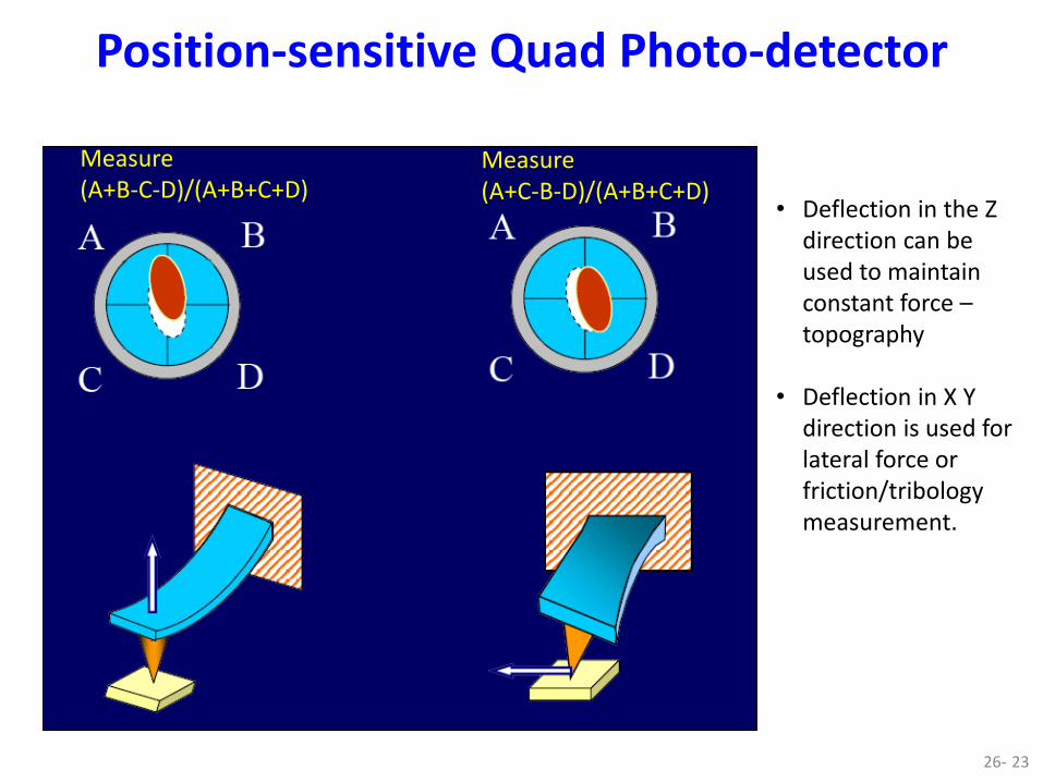
Position-sensitive Quad Photo-detector
26- 23
• Deflection in the Z
direction can be used to maintain constant force – topography
• Deflection in X Y direction is used for lateral force or friction/tribology measurement.
Measure (A+B-C-D)/(A+B+C+D)
Measure (A+C-B-D)/(A+B+C+D)

Modes of Operation Basic AFM Modes:
• Static or Contact mode (no vibrating tip): strong (replusive) – constant force or constant distance.
• Dynamic modes [non-contact and tapping modes] (vibrating tip): weak (attractive and repulsive).
More Advanced Modes:
• Liquid AFM • Magnetic Force Microscopy (MFM) • Lateral Force Microscopy (LFM): frictional
forces exerting a torque on the cantilever • Force Modulation Microscopy (FMM) • Electrostatic Force Microscopy (EFM) • Plus...
Samples:
• Conductors – metals, semiconductors... • Insulating materials – all types: oxides,
polymers, biological materials
26- 24

AFM Probe – Tip plus Cantilever
• Materials: Si, Si3N4
• Pyramidal, conical shapes
• Cantilever: 100-200 m long, 1-4 m thick Tip: 10-20 m; curvature radius r
• Contact tip: soft k < 1 N/m; r < 50 nm; f 15 kHz
• Non-contact tip: stiff k 20-100 N/m; r < 10 nm; f 200-400 kHz
• Non-contact sharper than contact tip
26- 25

AFM Tips
26- 26

Static vs Dynamic Mode Imaging
Static or Contact Mode
• Constant force deflection;
• Force in strong replusive regime;
• Tip in physical contact with the surface;
• “Soft” cantilever with stiffness less than force constant in atoms (10 nN/nm);
• Van der Waals forces.
Static Mode
• Good for imaging hard and shallow samples, samples with periodicity, and samples in liquid environments. Dynamic Modes
• Good for imaging soft (polymers, biomolecules), or delicate samples (with poor surface adhesion), samples in ultrahigh vacuum.
26- 27
Dynamic Modes: Non-contact or Frequency Modulation
• Constant force gradient deflection;
• Resonance frequency feedback;
• Force in weak attractive regime;
• Tip is oscillating 1-10 nm above the surface;
• “Stiff” cantilever with tip to sample forces about pN.
Tapping or Amplitude Modulation
• Constant force gradient deflection;
• Amplitude feedback
• Force in weak repulsive/attractive regime
• “Stiff” cantilever making intermittent contact with the surface.

26- 28

AFM: Applications
26- 29
Contact Mode: Au(111) polycrystalline film on a glass substrate
Non-contact Mode: Si(111) 7x7 Tapping Mode: Arene on graphite
http://www.asylumresearch.com/Gallery/Gallery.shtml

AFM: Applications
26- 30
Single-strand G4 DNA – 1x1 m2
C60 on KBr(001) – lower – Pawlak et al.
J Phys C 24 (2012) 084005.
Carbon nanotubes on mica

STM vs AFM: True Nanotools
26- 31
STM
• Real space imaging;
• Not true topographic imaging b/c it measures local electron density of states, not nuclear positions;
• High lateral and vertical resolution – atomic resolution;
• Probe electronic properties (LDOS – including spin states);
• Sensitive to noise;
• Image quality depends on tip conditions (atomically sharp, dirt, etc.);
• No direct chemical identification;
• Only for conductive materials.
AFM plus
• Real topographic imaging;
• Lower lateral resolution;
• Probe various physical properties: magnetic, electrostatic, hydrophobicity, friction, elastic modulus, etc.;
• Can manipulate molecules and fabricate nanostructures;
• Contact mode can damage the sample;
• Image distortion due to the presence of water;
• No direct chemical identification;
• Apply to both conducting and non-conducting materials, including polymers, biomolecules, ceramics.