frequency synthesizer requirements for future cellular ... · frequency synthesizer requirements...
TRANSCRIPT

i
University of Southern Queensland
Faculty of Engineering and Surveying
FREQUENCY SYNTHESIZER REQUIREMENTS FOR FUTURE CELLULAR RADIO SYSTEMS
(06-026)
A dissertation submitted by
Woo Mun Kit 0050014226
in fulfillment of the requirements of
Course ENG4111 and 4112 Research Project
towards the degree of
Bachelor of Engineering (Electrical and Electronics)
Submitted: November, 2006

ii
ABSTRACT This dissertation describes the research and experimentation on the future Third Generation (3G) requirements. This project makes used of an integrated Phase Locked Loop (PLL) frequency synthesizer evaluation board from Analog Devices Pte Ltd with an operating frequency range from 2.2 GHz to 2.45 GHz. The objective of this project is to evaluate the synthesizer requirements of future 3G mobile systems. By extrapolating from existing 3G systems and conducting some researches, it is able to make an educated guess on the frequency synthesizer requirements for the future 3G mobile systems. These requirements and performance are then compared to the hardware evaluation and software simulated findings retrieved from the evaluation board and its simulation software as well as from all other designs. Finally, from the outcome of these comparisons, it is able to conclude which designs are likely to be more suitable for future 3G mobile systems. Moreover, with this project, apart from giving the student a chance to predict the requirements for future 3G system and verified them in the near future, it also helps to create a good learning experience to any students who are very new to frequency synthesizer system but very much interested in getting to know its performance and how it actually functions.
For the first stage of the project, researches on both the current and future 3G requirements are carried out. At the same time, research on suitable frequency synthesizer techniques and evaluation boards are also conducted. With all the important parameters collected from the researches done for both the current and future 3G requirements, it can then be used as an input criteria in selecting a suitable PLL frequency synthesizer evaluation board from the available market for future 3G applications. Following the first stage, the second stage will includes hardware evaluation and software simulation on the suitable PLL frequency synthesizer evaluation board bought from Analog Devices Pte Ltd. However, due to some unforeseen circumstances, the hardware evaluation on the evaluation board is unable to carried out smoothly with all the important parameters required for future 3G applications measured as planned, thus another method to retrieve the values of these important parameters has been suggested. The suggested method is to replace the hardware evaluation portion by a software simulation using the simulation software provided by Analog Devices Pte Ltd. Finally, this dissertation also discusses the project constraints as well as the equipment and software limitations encountered during the whole project phase.

iii
University of Southern Queensland
Faculty of Engineering and Surveying
ENG4111 Research Project Part 1 & ENG4112 Research Project Part 2
Limitations of Use
The Council of the University of Southern Queensland, its Faculty of Engineering and Surveying, and the staff of the University of Southern Queensland, do not accept any responsibility for the truth, accuracy or completeness of material contained within or associated with this dissertation. Persons using all or any part of this material do so at their own risk, and not at the risk of the Council of the University of Southern Queensland, its Faculty of Engineering and Surveying or the staff of the University of Southern Queensland. This dissertation reports an educational exercise and has no purpose or validity beyond this exercise. The sole purpose of the course pair entitled “Research Project” is to contribute to the overall education within the student’s chosen degree program. This document, the associated hardware, software, drawings, and other material set out in the associated appendices should not be used for any other purpose: if they are so used, it is entirely at the risk of the user.
Professor R Smith Dean Faculty of Engineering and Surveying
iv
CERTIFICATION I certify that the ideas, designs and experimental work, results, analyses and conclusions set out in this dissertation are entirely my own effort, except where otherwise indicated and acknowledged. I further certify that the work is original and has not been previously submitted for assessment in any other course or institution, except where specifically stated. Woo Mun Kit Student Number: 0050014226
Signature
Date

v
ACKNOWLEDGEMENTS First of all, I would like to express my appreciation and gratitude to my supervisor, Associate Professor Jim Ball, for his ideas and guidance he had given to me throughout the duration of this project. At the same time, I would like to take this opportunity to thank Mr Ian Collins, the Applications Engineer from Analog Devices for taking up the time to answer all my questions on the ADF4360-1 evaluation board and giving me invaluable support. I would also like to thank Ms Ng Kim Ching and Mr Tee Keng Hoe, both colleagues from my workplace for providing me with the access to some of the measuring equipment and allowing me to use their work bench to conduct measurements. Finally, I would like to thank University of Southern Queensland, Faculty of Engineering and Surveying, for sponsoring this project and giving me the chance to have this project as my Final Year Project as well as those who have helped me throughout the duration of this whole project.

vi
TABLE OF CONTENTS
1. INTRODUCTION ................................................................................................. 1
1.1 Background on Evolution of Cellular Radio ...................................................... 1 1.2 Background on Frequency Synthesis.................................................................. 2 1.3 Project Objectives............................................................................................... 3
1.3.1 Specific Objectives ...................................................................................... 4
1.4 Project Methodology .......................................................................................... 4 1.5 Project Constraints.............................................................................................. 6 1.6 Dissertation Overview ........................................................................................ 6
2. BACKGROUND.................................................................................................... 8
2.1 Generations of Cellular Radio Systems.............................................................. 8
2.1.1 First Generation (1G) System ..................................................................... 8 2.1.2 Second Generation (2G) System................................................................. 8 2.1.3 Migration to Third Generation (3G) System............................................... 9
2.2 Present and Future 3G Cellular Radio Systems Standards............................... 10
2.2.1 Wideband Code Division Multiple Access (WCDMA) ........................... 14
2.3 Review of Frequency Synthesizer Literature ................................................... 17
2.3.1 Direct Digital Synthesis (DDS)................................................................. 17 2.3.2 Phase Locked Loop (PLL) ........................................................................ 18
2.4 Comparative Analysis on Frequency Synthesizer Evaluation Boards ............. 21
3. EVALUATION BOARD..................................................................................... 24
3.1 Description on Evaluation Board...................................................................... 24 3.2 Capabilities of the Evaluation Board................................................................ 27 3.3 ADF4360 Evaluation Board Programmable Software ..................................... 27 3.4 Measurements and Difficulties Encountered.................................................... 32
4. SIMULATION SOFTWARE............................................................................. 39
4.1 Description on Simulation Software................................................................. 39 4.2 Functions of ADIsimPLL ................................................................................. 39 4.3 Usage of ADIsimPLL....................................................................................... 46
5. RESULTS............................................................................................................. 49
5.1 Results on Hardware Evaluation ...................................................................... 50 5.2 Results on Software Simulation ....................................................................... 54
6. DISCUSSION AND CONCLUSIONS............................................................... 63
6.1 Results Discussion............................................................................................ 63 6.2 Conclusion........................................................................................................ 67 6.3 Suggestions for Future Work............................................................................ 69
7. REFERENCES .................................................................................................... 70

vii
8. BIBLIOGRAPHY................................................................................................ 72
9. APPENDICES...................................................................................................... 74
9.1 Appendix A – Project Specifications................................................................. 74 9.2 Appendix B – Timelines Planning and Work Breakdown Structure (WBS)..... 76 9.3 Appendix C – Risk Assessment and Management ............................................ 78
9.3.1 Project Risks .......................................................................................... 78 9.3.2 Safety Issues........................................................................................... 78
9.4 Appendix D – Resource Requirements and Planning........................................ 81 9.5 Appendix E – Articles requesting for higher frequency band below 3 GHz ..... 83 9.6 Appendix F – Generated Output Results from ADIsimPLL v.3.0 Software ..... 85 9.7 Appendix G – Port Setup Tab from Code Loader v.2.2.0 Software.................. 90 9.8 Appendix H – PLL Tab from Code Loader v.2.2.0 Software............................ 91 9.9 Appendix I – Weekly Progress Report for Wk 637........................................... 92 9.10 Appendix J – 1st Measurements on all Test Points in ADF4360-1EB1............ 93 9.11 Appendix K – 2nd Measurements on all Test Points in ADF4360-1EB1 ......... 94

viii
LIST OF FIGURES
Figure 1: Methodology Flowchart.................................................................................4 Figure 2: Roadmap from 2G to 3G Systems..............................................................10 Figure 3: The Five 3G Standards under IMT-2000...................................................11 Figure 4: WARC-92 IMT-2000 Spectrum Allocation in Europe, USA and Japan.14 Figure 5: Difference between 2G services using TDMA/CDMA and 3G services
using WCDMA ............................................................................................15 Figure 6: Basic Block Diagram of a Direct Digital Synthesis (DDS)........................17 Figure 7: Basic Block Diagram of a Phase Locked Loop (PLL) ...............................18 Figure 8: Picture of the ADF4360-1 Evaluation Board.............................................24 Figure 9: Functional Block Diagram of ADF4360-1 Synthesizer IC Chip inside the
Evaluation Board ........................................................................................25 Figure 10: Main Interface Page of the ADF4360 Evaluation Board Programmable
Software.......................................................................................................28 Figure 11: Screenshot on the Muxout Options menu................................................30 Figure 12: Screenshot on the RF Output Frequency menu ......................................31 Figure 13: Screenshot on the Registers menu............................................................32 Figure 14: Picture on the ESD Wrist Strap................................................................33 Figure 15: Picture on the SMA Male Plug to BNC Female Jack Connector..........34 Figure 16: Picture on the Tektronix TDS3014B High Speed Oscilloscope..............34 Figure 17: Picture on the LeCroy Wave Surfer 424 High Speed Oscilloscope.......35 Figure 18: Picture on the USB to 25-Pin Female (Parallel) Adaptor Cable............37 Figure 19: Picture on the Trans PC Card - Universal Parallel Port PCMCIA card
....................................................................................................................37 Figure 20: Screenshot on the Menu for specifying the Frequency Requirements..40 Figure 21: Screenshot on the Menu for selecting a PLL IC chip .............................41 Figure 22: Screenshot on the Menu for selecting the Loop Filter Configurations .42

ix
Figure 23: Screenshot on the Menu for selecting a VCO ..........................................43 Figure 24: Screenshot on the Menu for selecting the Reference Frequency...........44 Figure 25: Screenshot showing the Data Panel and the Results Panel....................45 Figure 26: Example showing the Usage of the Marker Feature...............................47 Figure 27: Example showing the Usage of the Save Trace Feature.........................47 Figure 28: Test Point T1 Output Waveform using Tektronix TDS3014B..............50 Figure 29: Test Point T2 Output Waveform using Tektronix TDS3014B..............50 Figure 30: Test Point T1 Output Waveform using LeCroy Wave Surfer 424........51 Figure 31: Test Point T2 Output Waveform using LeCroy Wave Surfer 424........52 Figure 32: Test Point T3 Output Waveform using LeCroy Wave Surfer 424........53 Figure 33: ADIsimPLL Starting Options for this Proj ect.........................................54 Figure 34: Absolute Frequency Error Graph............................................................56 Figure 35: Output Phase Error Graph.......................................................................56 Figure 36: Total Phase Noise Graph at 2.35 GHz with Loop Bandwidth of 80 KHz
....................................................................................................................60 Figure 37: Frequency Graph with Loop Bandwidth of 80 KHz...............................60 Figure 38: Phase Noise Graph at 2.35 GHz with Loop Bandwidth of 80 KHz .......61

x
LIST OF TABLES
Table 1: Advantages and Disadvantages of the 3 Synthesis Techniques...................3 Table 2: UMTS Frequencies Allocated and Usage for 3G Mobile Systems............14 Table 3: 3G Spectrum Usage in Singapore.................................................................16 Table 4: Different Frequency Synthesizer Evaluation Board Comparison Table..21 Table 5: Features of ADF4360-1 Evaluation Board..................................................27 Table 6: Truth Table for Control Bits C2 and C1.....................................................28 Table 7: Phase Noise with Loop Bandwidth of 10 KHz............................................55 Table 8: Phase Noise with Loop Bandwidth of 10 KHz............................................57 Table 9: Frequency and Phase Locking Time with Loop Bandwidth of 10 KHz ...57 Table 10: Phase Noise with Loop Bandwidth of 790 KHz ........................................58 Table 11: Frequency and Phase Locking Time with Loop Bandwidth of 790 KHz58 Table 12: Phase Noise with Loop Bandwidth of 80 KHz..........................................59 Table 13: Frequency and Phase Locking Time with Loop Bandwidth of 80 KHz .59 Table 14: Comparison Table 1 on Requirements between the Synthesizer Design
created by ADIsimPLL and the other manufacturer's Frequency Synthesizer Design......................................................................................64
Table 15: Comparison Table 2 on Requirements between the Synthesizer Design
created by ADIsimPLL and the other manufacturer's Frequency Synthesizer Design......................................................................................65
Table 16: Comparison Table on Requirements between Synthesizer Design created
by ADIsimPLL and the Future 3G predicted Synthesizer Design.........66 Table 17: Table on the Measuring Equipment used in the Project..........................81

xi
GLOSSARY OF TERMS 3G
Term used to describe mobile systems evolved from the first and second generation of mobile communications networks. 3G systems feature higher data transmission speeds, advanced services and typically make use of new allocations of radio spectrum not available to operators of 2G networks.
3GPP 3GPP basically stands for Third Generation Partnership Project. It is a collaboration agreement that was established in December 1998 whereby this collaboration agreement brings together a number of telecommunications standards bodies that are known as Organizational Partners. The current Organizational Partners are ARIB, CCSA, ETSI, ATIS, TTA, and TTC.
Bell Lab Known as Bell Laboratories and formerly known as AT&T Bell Laboratories and Bell Telephone Laboratories was the main research and development arm of the United States Bell System.
CDMA Code Division Multiple Access or CDMA is a form of multiplexing (not a modulation scheme) and a method of multiple access that does not divide up the channel by time (as in TDMA), or frequency (as in FDMA), but instead encodes data with a special code associated with each channel and uses the constructive interference properties of the special codes to perform the multiplexing.
CDMA2000
Code Division Multiple Access 2000 is a family of Third Generation (3G) mobile telecommunications standards that use CDMA, a multiple access scheme for digital radio, to send voice, data, and signalling data (such as a dialed telephone number) between mobile phone and cell sites.
FDD
Frequency division duplex (FDD) is the application of frequency division multiple access to separate outward and return signals. The uplink and downlink sub-bands are said to be separated by the "frequency offset". Frequency division duplex is much more efficient in the case of symmetric traffic. It makes radio planning easier and more efficient since base stations do not "hear" each other (as they transmit and receive in different sub-bands) and therefore will normally not interfere each other.
FDMA Frequency Division Multiple Access or FDMA is an access technology that is used by radio systems to share the radio spectrum. The terminology “multiple access” implies the sharing of the resource amongst users, and the “frequency division” describes how the sharing is done: by allocating users with different carrier frequencies of the radio spectrum.

xii
GSA The Global mobile Suppliers Association, is the forum for, and represents, the leading GSM/3G suppliers world-wide. It is an organization created to meet suppliers’ needs and already represents over 80% of GSM/3G market share globally.
GSM Second Generation (2G) mobile system originally developed in Europe, using a TDMA access radio interface combined with Frequency Division Multiple Access (FDMA). Oriented to voice and circuit mode data.
HSDPA Currently being specified by 3GPP as an enhancement to the UMTS Terrestrial Radio Access Network (UTRAN) with the goal of enabling packet data transmission in the downlink at theoretical speeds of up to 10 Mbps.
ITU International organisation within the United Nations System where governments and the private sector coordinate global telecom networks and services.
PSB Corporation
It is a one-stop integrated solution provider to help you achieve business excellence through people, products and processes. Their Safety Mark Scheme tests and certifies all electrical products for conformity to the Consumer Protection Safety Requirements.
SMA SMA stand for Sub-Miniature Type-A. SMA connectors provide an economic solution for RF and microwave inter-connection up to 18GHz. It is a dielectrically loaded, sexed connectors for applications where connections are made only a few times, i.e., less than 500 times. The SMA connectors are compatible with 3.5mm and 2.92mm connectors.
Spectrum Analyser
A radio receiver with a swept local oscillator that displays frequency against amplitude on a Cartesian display.
TDMA Time division multiple access or TDMA is a technology for shared medium, usually radio networks. It allows several users to share the same frequency by dividing it into different timeslots. The users transmit in rapid succession, one after the other, each using his own timeslot. This allows multiple users to share the same transmission medium (e.g. radio frequency) while using only the part of its bandwidth they require.
TD-SCDMA Time Division-Synchronous Code Division Multiple Access is a 3G mobile telecommunications standard, being pursued in the People’s Republic of China by the Chinese Academy of Telecommunications Technology (CATT), Datang
xiii
and Siemens AG, in an attempt to develop home-grown technology and not be "dependent on Western technology”.
UMTS 3G system standardised by ETSI under 3GPP along with other regional standards organisations.
WARC’92 ITU conference that provided a framework at global level for spectrum to support growth in mobile services towards 3G. Support for non-voice services and international roaming were essential requirements in the brief to identify new spectrum for 3G.
WCDMA Wideband Code Division Multiple Access is a 3G technology that increases data transmission rates in GSM systems by using the CDMA air interface instead of TDMA. In the ITU's IMT-2000 3G specification, WCDMA has become known as the Direct Sequence (DS) mode.
WiMAX WiMAX (World Interoperability for Microwave Access, Inc.), based on the IEEE 802.16 standard, is expected to enable true broadband speeds over wireless networks at a cost point to enable mass market adoption. WiMAX is the only wireless standard today that has the ability to deliver true broadband speeds and help make the vision of pervasive connectivity a reality.

xiv
Acronyms and Abbreviations Acronyms Abbreviations 3G Third Generation 3GPP Third Generation Partnership Project AMPS Advanced Mobile Phone System ARIB Association of Radio Industries and Businesses ATIS Alliance for Telecommunications Industry Solutions BNC Bayonet Neill Concellman CDMA Code Division Multiple Access CDMA2000 Code Division Multiple Access 2000 CE Chip Enabled CLK Serial Clock Input CMOS Complementary Metal Oxide Semiconductor CP Charge Pump DA Direct Analog DAC Digital-to-Analog Converter DDS Direct Digital Synthesis DECT Digital Enhanced Cordless Telecommunications DS Direct Sequence DSL Digital Subscriber Line DSP Digital Signal Processing EDGE Enhanced Data Rates for Global Evolution ESD Electro Static Discharge ETSI European Telecommunications Standards Institute FDMA Frequency Division Multiple Access FDD Frequency Division Duplex FS Frequency Synthesizer GUI Graphic User Interface GPRS General Packet Radio Service GPS Global Positioning System GSA Global mobile Suppliers Association GSM Global System for Mobile communications HSDPA High Speed Downlink Packet Access HSPA High Speed Packet Access IC Integrated Circuit iDEN Integrated Digital Enhanced Network IMT International Mobile Telecommunications I/O Input/Output IP Internet Protocol IPv4 Internet Protocol version 4 IPv6 Internet Protocol version 6 ITU International Telecommunications Union IS-95 Interim Standard 95 IS-136 Interim Standard 136 LE Load Enable LO Local Oscillator LSB Least Significant Bit

xv
Acronyms Abbreviations MC Multi-Carrier MSB Most Significant Bit NMT Nordic Mobile Telephone PC Personal Computer PCMCIA Personal Computer Memory Card International Association PDF Phase Detector Frequency PFD Phase Frequency Detector PSB Productivity and Standards Board PSTN Public Switched Telephone Network RAMP Risk Assessment and Management Plan RF Radio Frequency RTMI Radio Telefono Mobile Integrato SMA Sub-Miniature Type-A SMS Short Message Service TACS Total Access Communication System TDD Time Division Duplex TDMA Time Division Multiple Access TD-SCDMA Time Division-Synchronous Code Division Multiple Access TTC Telecommunication Technology Committee UMTS Universal Mobile Telecommunications System USA United States of America USB Universal Serial Bus UTRA Universal Terrestrial Radio Access UWC-136 Universal Wireless Communication 136 VCO Voltage Controlled Oscillator WARC’92 World Administrative Radio Conference 1992 WBS Work Breakdown Structure WCDMA Wideband Code Division Multiple Access WiMAX World Interoperability for Microwave Access WLAN Wireless Local Area Network

1
1. INTRODUCTION
This is a project dissertation on the project topic of Frequency Synthesizer Requirements for Future Cellular Radio Systems (06-026). Basically, this dissertation provides some background information on the current Third Generation (3G) mobile radio systems as well as the frequency synthesizer techniques. It also includes a detailed documentation on what are tasks that had been planned to be accomplished as well as how these tasks are being executed in order fulfill the completion of the project. Last but not least, the results collected will be discussed and a conclusion will be made in the last 2 chapters of this project dissertation.
1.1 Background on Evolution of Cellular Radio
Recently the Third Generation (3G) systems had become a very popular topic among all people due to the fact that 3G services had already been adopted in most of the developed countries. The demand for 3G mobile data services is real. Nowadays, not only youngsters but also working adults had been carrying a 3G mobile phone around them. Consumers and business users have consistently demonstrated strong interest in trying new services that combine mobility with content and personalization such as 3G services. According to UMTS frequencies allocated and usage for 3G mobile systems in Europe and some Asia countries (including Singapore), the operating frequency range for 3G mobile services based on the Frequency Division Duplex (FDD, WCDMA) are 1920 MHz - 1980 MHz for uplink and 2110 MHz - 2170 MHz for downlink. With a channel spacing of 5 MHz, the total bandwidth allocated for 3G mobile WCDMA services is 120 MHz, which will result in having a total number of 24 channels. The frequency range of 1900 MHz – 1920 MHz and 2010 MHz - 2025 MHz are allocated for Time Division Duplex, Time Division/Code Division Multiple Access (TDD, TD/CDMA) uplink and downlink usage while the frequency range of 1980 MHz – 2010 MHz and 2170 MHz - 2200 MHz are for Satellite uplink and downlink used (UMTS Forum, ‘WARC-92 frequencies of IMT-2000’ resolution, 2000). As of current situation, 3G Wideband Code Division Multiple Access (WCDMA) is the leading mobile 3G system globally with 112 commercial networks in 49 countries. The number of WCDMA subscriptions is estimated to be rapidly approaching 80 million worldwide. Over 50% of WCDMA license holders globally have brought their 3G services to the market. On 8 of August 2006, Global mobile Suppliers Association (GSA) confirms that 44 suppliers have launched 407 3G/WCDMA devices. It means ‘221 new products worldwide came to market in the past 12 months, representing almost 120% growth. The number of WCDMA device suppliers increased from 26 to 44 in the same period’ (GSA, 2006). All of these evidences clearly showed that users have already accepted such new technology and services, which implies 3G evolutions, had finally come. However, due to this fast changing pace in the Telecommunications industry, many of us will be thinking what will be the next technology coming up to replace 3G systems or what will be the future or post 3G systems going to be like. We are now unable to tell

2
anything till International Telecommunications Union (ITU) finally announces news on future 3G systems. However, with this project, it is able to let the audience to have a feel first on what would future 3G system going to be like and the requirements differences between the current 3G system and the future 3G system. At the same, this project will provide students a chance to gain forward expertise in one of the most rapidly developing fields within engineering as well as to have the opportunity to gauge what the future 3G systems will be like. With this project in place, it will also helps to create good learning ground to students who have interest in this topic but very new to frequency synthesizer and 3G systems. All these can be done by the means of investigating the current frequency synthesizers available in the market, evaluate their synthesizer requirements with respect to the requirements for the future 3G mobile systems and finally conclude which frequency synthesizer’s designs are likely to be more suitable for future 3G mobile systems.
1.2 Background on Frequency Synthesis
A frequency synthesizer can be defined as a system that generates one or many frequencies derived from a single time base (reference frequency), in such a way that the ratio of the output to the reference frequency is a rational fraction. There are 3 main conventional techniques being used currently for sine-wave synthesizers and they are all common throughout the industry. One of the most common and popular techniques used in the current Third Generation (3G) mobile system industry is the Phase Locked Loop synthesis or what we normally called as PLL synthesis. Basically, the Phase Locked Loop (PLL) is a feedback mechanism locking its output frequency to a reference.
PLL synthesizers can be found almost everywhere in the communication industry. It can be found in the most sophisticated radar systems or the most demanding satellite communication terminals as well as in our daily household electronic devices such as the car radios and home entertainment stereo systems. The reason why PLL synthesizers are so popular is due to its attractive characteristics of simplicity and economics.
The second technique for sine-wave synthesizer is known as Direct Analog (DA) frequency synthesis. In this technique, a group of reference frequencies is derived from the main reference; and these frequencies are mixed and filtered, added, subtracted or divided according to the required output. However, there will be no feedback mechanisms in the basic technique. Although this technique offers excellent spectral purity and excellent switching speed, however it is usually much more complicated than PLL to execute and hence, when comes to implementation, it tends to be more expensive.
The third technique will be the Direct Digital Synthesis (DDS), which uses Digital Signal Processing (DSP) circuitry and techniques to create, manipulate, and modulate a signal digitally and finally convert this digital signal into its analog form by using a Digital-to-Analog Converter (DAC). There is another technique called fractional-N PLL synthesis, which is a combination of both DDS and PLL. In layman term, it operates

3
like a DDS within the PLL architecture. Nowadays, it is actually quite common to see combinations of PLL and DDS or DA and DDS. From time to time all these 3 techniques are used in one design by designers so as to optimize the design since we all know nowadays an increase in the applications and demands means an increase in the system complexity.
In this project, we will focus more on PLL synthesis technique since it is still widely used in the 3G mobile systems and it is much simpler to be implemented for future 3G mobile systems. In addition, the PLL synthesis technique has a very wideband operating frequency, which is more suitable for future 3G applications as compared to DDS since the DDS technique have a limited bandwidth of about 400 to 500 MHz for its operating frequency (Egan, 1990). The tabulated table below highlights the different advantages and disadvantages of these 3 synthesis techniques.
Table 1: Advantages and Disadvantages of the 3 Synthesis Techniques
1.3 Project Objectives
The objective of this project is to evaluate the synthesizer requirements of future 3G mobile systems, which involve a mixture of hardware evaluation and software simulation. By extrapolating from existing 3G systems it will allow the student to make an educated guess at the synthesizer requirements for the future 3G mobile radio systems and compared these requirements and the performance to the actual measured and simulated findings from the frequency synthesizer evaluation board as well as other designs and the simulation software. Finally, conclude which designs are likely to be
Synthesis Techniques
Advantages Disadvantages
Phase Locked Loop (PLL) synthesis
• Simple in design • Moderate to good switching
speeds • Very wideband operating
frequency • Easy to implement • Low Cost
• Resolution is complicated to achieved
• Good quality oscillators are quite bulky
• Digital modulation is complicated to apply with sufficient accuracy
Direct Analog (DA) synthesis
• Very high switching speeds • Very wideband operating
frequency • Spectral purity is excellent
• Quite bulky in size since it requires much hardware
• Expensive in Cost • Digital or analog modulation
is complicated to apply
Direct Digital Synthesis (DDS)
• Simple and compact • Very high switching speeds • Good resolution very easy to
achieved • Digital producibility
• Limited bandwidth of about 400 to 500 MHz for operating frequency
• Technology is not as mature as PLL and DA

4
suitable for 3G and future 3G mobile systems. Specific objectives and the constraints for the project are illustrated in the later sections of this dissertation. Basically, this project can be broken down into 3 different parts. The first part of the project involves research and investigation on the current 3G and future 3G requirements as well as on the frequency synthesizer evaluation board that are suitable for future 3G applications. The second part will include the evaluation of this suitable frequency synthesizer evaluation board via hardware and simulation software. The last part of this project will consist of comparison of the results or the parameters values collected from the evaluation process with respect to the future 3G requirements and other frequency synthesizer evaluation boards from other manufacturers.
1.3.1 Specific Objectives
The specific objectives or tasks for this project are reflected in the Project Specifications under Appendix A. A Work Breakdown Structure (WBS) and a resource tracking plan based on the Project Specifications, which denotes the planned timelines for major milestones or activities that need to be completed in terms of number of weeks are also attached as Appendix B inside this project dissertation.
1.4 Project Methodology
The methodology adopted in this project is based on the timeline with respect to various milestones or objectives defined in order for the completion of the project. This is illustrated in the flowchart shown in Figure 1 below.
Figure 1: Methodology Flowchart
Methodology
Research and Review on required information
Sourcing for available human and non-human resources
Planning stage
Measuring and Simulating
Evaluating and Comparing
Recommendation and Conclusion
Documentation and Reporting
5
Planning stage is the first and the most important milestone to be accomplished. Without proper planning, the project will not be able to run smoothly and many things such as risks and resources may not be defined or identified beforehand. Planning includes identification of the tasks require to be completed as well as the overall general planning needed to run the project. The completion of the Project Specifications is also considered as part of the planning stage because it defines the way of working together with the specific tasks in the project that need to be completed within the given timelines. With the basic understanding of the requirements and tasks identified in the Project Specifications, research work started off first by concentrating on information gathering activities, such as researching of current 3G systems as well as reviewing of the frequency synthesizer technologies and carrying out a survey on the current available frequency synthesizer evaluation boards in the market. The main aim for the Research and Review on the required information milestone is to get to know the background knowledge that is essential in order to complete this project successfully. With all the research done and information gathered during the research, it can helps to select a more suitable frequency synthesizer evaluation board that is available in the current market for this project. Furthermore, by doing research on the relevant topics for the project will also helps to provides more information and details in writing the project dissertation. When all the research is almost completed, a suitable frequency synthesizer evaluation board will be able to be selected for this project use. Before started off to measure the performance of this evaluation board, non-human resources such as the spectrum analyser, oscilloscope and etc needs to be defined and planned. This forms the third milestone on the Sourcing for available human and non-human resources under the methodology flowchart. After the sourcing of the resources, measuring and simulating of the performance such as the switching time requires for changing channels will be carried out. With all the hardware evaluation measurement findings completed on this evaluation board as well as the simulated findings done using the simulation software, this evaluation board synthesizer design will be evaluated against future requirements for 3G and future 3G systems to see if such design is it suitable for future 3G systems. At the same time, other synthesizer designs will also be evaluated and compared to this evaluation board synthesizer design. The main aim for the Measuring and Simulating as well as the Evaluating and Comparing milestones is to find out the best suitable synthesizer designs for future 3G systems through the experiment and comparison with the requirements collected from all different sources. The advantages and reasons behind for selecting this best suitable synthesizer designs for future 3G systems will then be elaborated in the Recommendation and Conclusion milestone. Last but not least, all the information and data collected from the first milestone to the second last milestone will be finally documented and put into proper wordings in the project dissertation.

6
1.5 Project Constraints
From the start of the project till now, there are a few constraints encountered. They are as follows:
• Not all of the important parameters on the current 3G radio systems are found, only some of these parameters such as the operating frequency range, are being found to use for comparison to the specifications of the evaluation boards available in the market. This is due to the fact that a lot of information on these parameters are not available or clearly specified in places like the library books or the Internet and a lot of this related information such as Third Generation Partnership Project (3GPP) specifications are not easy accessible. Most of the 3G websites (e.g. 3GPP) which has information that are sensitive, requires to be a subscribed member or needs to request for access rights in order to view these information within the site. Another factor is that these parameters are not always standard in values as it will also need to depend on the type of frequency synthesizer the system adopt and other related factors. With this constraint, we can only depend on the few parameters found to look for a suitable frequency synthesizer evaluation board.
• The evaluation board needs to be within the budget allocated of AUD$200, hence with this constraint, it narrow the scope of finding a suitable frequency synthesizer evaluation board available in the market.
1.6 Dissertation Overview
In order to gain a better understanding of the theory of the frequency synthesizer as well as the present and future 3G cellular radio standards that are discussed in this dissertation, some review of the background for these 2 points needs to be made. Thus, in Chapter 2 of this dissertation, it will first present a summary of the different generations of the Cellular Radio Systems. Then, it will follow up by discussing the present and future 3G Cellular Radio Systems Standards and some background information on the current 3G technology. It will then go on to elaborates on some theory and background knowledge on the WCDMA techniques, which are currently used in 3G mobile services. The second portion of Chapter 2 will includes a summary of the relevant theory of frequency synthesizer in particular the Phase Locked Loop frequency synthesizer. It will also describe each and every important parameter in a frequency synthesizer that is required for selecting a suitable frequency synthesizer evaluation board for future 3G systems applications. A comparison table between different manufacturers’ frequency synthesizer evaluation board are also illustrated in this chapter. Finally, the project constraints are also illustrated at the end of Chapter 2. In Chapter 3, hardware evaluation and experimental techniques are discussed here. The discussion includes some descriptions on the frequency synthesizer evaluation board purchased from Analog Devices Pte Ltd, how the evaluation board actually functions as well as the measurement process conducted so far on the evaluation board. It also

7
includes a short description on the Analog Devices program register software that comes together with the evaluation board. Lastly, it will also discuss on the limitations and difficulties faced during the measuring and evaluating process on the evaluation board. In Chapter 4, software simulation techniques are discussed here. This will includes some descriptions on the ADIsimPLL simulation software from Analog Devices Pte Ltd, how this simulation software actually works as well as the usage of this simulation software. In Chapter 5, principally, it presents the results of the measurements conducted on the ADF4360-1 evaluation board itself as well as the results collected from using the ADIsimPLL simulation software. It does not really goes into much discussion on the results collected from both the hardware evaluation and software simulation. The results discussion will be done in Chapter 6 instead. In Chapter 6, it will cover both the results discussion and the conclusion of this project. The output results from both the hardware evaluation and software simulation are then compared with those future 3G requirements collected from the research that had been conducted in the earlier phase of the project duration. These results are also compared with the other manufacturers’ frequency synthesizer evaluation board performance based on their evaluation board datasheets. At the same time, this chapter also provides a final overview of the work involved and summarizes the results. It also makes recommendations for future work for this project and finally marks a conclusion chapter in this dissertation.

8
2. BACKGROUND
To first start with the project, there is need to find out more about the different generation of cellular radio systems, the current 3G mobile radio standards and techniques used, and the plans for future 3G. It is also an essential to understand Phase Locked Loop synthesizers in detail, as there is a need to look for a suitable frequency synthesizer evaluation board for future 3G systems evaluation purposes in this project. Below sections will illustrate more on these few literature review points.
2.1 Generations of Cellular Radio Systems
2.1.1 First Generation (1G) System
In mid 1980’s, the very first hand held mobile phone was commercially launched by one of the mobile phone company named Motorola. This first truly portable hand held phone makes use of the First Generation (1G) mobile communications systems, offering simple wireless voice services based on analog technology. Some of these 1G systems include Nordic Mobile Telephone (NMT), Advanced Mobile Phone System (AMPS), Total Access Communication System (TACS), and Radio Telefono Mobile Integrato (RTMI).
One of the more popular First Generation mobile systems is the AMPS, which is developed by Bell Labs, and officially introduced in United States of America (USA) in 1983 (Wikipedia, Oct 2006). The radio signals used in this AMPS 1G networks are purely analog and the call is not encoded but only modulated to higher frequency (typically 150 MHz and above). In general, 1G systems provide only low quality voice services and were very limited in capacity. Therefore, eventually, 1G systems services did not extend across geographic areas.
2.1.2 Second Generation (2G) System
In the 1990s, the Second Generation (2G) mobile phone systems such as Global System for Mobile communications (GSM), Interim Standard 136 or what we call as IS-136, Integrated Digital Enhanced Network (iDEN) and Interim Standard 95 (IS-95) had been introduced into the market. The digital Second Generation (2G) systems developed in Europe were mainly GSM, based on Time Division Multiple Access (TDMA) technology and in USA mainly IS-95, which is based on Code Division Multiple Access (CDMA) technology.
CDMA technology permits several radios to share the same frequencies. Unlike TDMA, with CDMA, all radios can be active at all the time, because network capacity does not directly limit the number of active radios. Since larger numbers of phones can be served by smaller numbers of cell-sites, CDMA-based standards have a significant economic advantage over TDMA-based standards.
With the introduction of 2G systems, it simply breaks the trend of having a very large size hand held phones (which was used in 1G systems) towards having a tiny hand held devices weighing just about 100 to 200 grams. This change was made possible through

9
new improvements on technologies such as more advanced batteries and more energy-efficient electronics, but also it was largely related to the higher density of cellular sites caused by increasing usage levels based on the higher demands from the subscribers.
In 2G networks, they are using digital radio signals rather than analog radio signals. When comparing to 1G systems, the call is encoded to digital signals in 2G systems unlike in 1G systems, the call is only modulated to a higher frequency. Generally, 2G systems provide better voice quality, higher capacity, global roaming capability as well as lower power consumption as compare to 1G systems. 2G systems also offer support for simple non-voice services such as the Short Message Service (SMS) that 1G systems can never provides.
However, there are a few drawbacks of 2G systems. One of it is that, different 2G technologies do not interoperate. There are also difficulties with roaming between GSM and IS-95 countries. In addition to these two drawbacks, the low data rate of 9.6 Kbps provided by the 2G systems (GSM) is not sufficient to meet subscriber demands for new and faster non-voice services on the move. Thus, Third Generation (3G) systems had been created to aim to resolve these problems encountered with 2G systems, by promising global roaming across 3G standards, as well as support for higher data rates and multimedia applications (Holma & Toskala, 2000).
2.1.3 Migration to Third Generation (3G) System
In the evolution from 2G to 3G systems, different migration paths have been identified for GSM-centric and IS-95 or CDMA-centric systems. The objective is to enhance spectral efficiency and network capacity. Mobile operators around the world had migrated their networks either towards 2.5G for General Packet Radio Service (GPRS) or 3G systems directly. Unlike 2G systems, 2.5G and 3G systems will feature packet-switched technology. Packet-switching means that dedicated circuits do not need to be established between communicating devices, and network resources are used only when actual data is transmitted. This means that it is in “always active” connectivity mode for subscribers. The billing for 2.5G and 3G services, are mainly based on either packet-based, time-based or a mixture of the two.
GSM-centric operators have the option to implement General Packet Radio Service (GPRS) and/or Enhanced Data Rates for Global Evolution (EDGE) prior to 3G rollout. GPRS provides a relatively easy upgrade of existing 2G networks to support higher data rates. Commonly considered a 2.5G technology, GPRS offers a theoretical maximum 171.2 Kbps data rate, when all 8 time slots are fully utilised at once. However, it is more likely that subscribers would only be allocated 2 to 4 time slots at one time, thus this will significantly lowered the actual data rate. In addition, initial GPRS deployments would only provide point-to-point support, meaning that subscribers can only communicate with one party at any one time. ‘At present, most of the European operators have already announced commercial GPRS rollouts. GPRS roaming trials had also been conducted in Asia in the last few years’ (GSA, 2006). This means that mobile data services had already been taken off with the advent of higher data rates offered by GPRS. Beyond GPRS, operators have the option of implementing EDGE or migrating directly to Wideband Code Division Multiple Access (WCDMA). EDGE enhances GPRS and

10
offers data rates of up to 384 Kbps through the use of a more efficient modulation technique. Another advantage of EDGE over GPRS is its ability to support for point-to-multipoint communication. Operators without 3G licenses may be able to offer GPRS or EDGE instead. However, some operators may prefer a direct 3G implementation over additional infrastructure costs in association with EDGE. Also, a significant challenge facing GSM migration is handset compatibility. New handsets will be required for every migration step, no matter if it is for GPRS, EDGE, or WCDMA. With the advent of 3G systems, and its accompanying mobile applications and services, mobile devices will become more than just a mobile phone or a basic electronic organiser. Hybrid devices will appear in the near future, supporting not only the traditional voice, but also video streaming and downloads, as well as Internet and intranet access. 3G's high data rate capabilities will allow the convergence of value-added data and voice services on the same mobile device. This will dramatically change the way people communicate, work and carry out their daily lives. Coupled with emerging technologies like Bluetooth, Global Positioning System (GPS) and biometrics authentication, there is enormous possibility for innovative applications to emerge. The diagram below shows a clear roadmap from the Second Generation (2G) mobile systems to 2.5G mobile systems and finally to the Third Generation (3G) mobile systems.
Figure 2: Roadmap from 2G to 3G Systems
2.2 Present and Future 3G Cellular Radio Systems Standards
Quite differently from 2G systems, however, in order to support the process and progress of the 3G cellular radio systems, standards had been laid down beforehand. The meaning of 3G has been standardized in the International Mobile Telecommunications-2000 (IMT-2000) standardization processing. The International Mobile Telecommunications-2000 (IMT-2000) is the global standard specially defined for Third Generation (3G) wireless communications. With IMT-2000 standard, it did

11
not really standardize on a technology, but rather on a set of requirements (for example, 2 Mbps maximum data rate at indoors, 384 Kbps at outdoors). IMT-2000 is basically defined from a set of interdependent International Telecommunication Union (ITU) Recommendations. ITU main activities on IMT-2000 consist of international standardisation, which includes the frequency spectrum and technical specifications for radio and network components and etc.
‘The main aim of IMT-2000 is to harmonize worldwide 3G systems to provide global roaming’ (3G Phones, 2006). However, harmonizing so many different standards proved to be extremely difficult. As a result, there are a total of five different standards grouped together under the IMT-2000 label. These five different standards are as follows:
• WCDMA • CDMA2000 • TD-CDMA/TD-SCDMA • DECT • UWC-136
The diagram shown below illustrates these five 3G standards under IMT-2000 label.
Figure 3: The Five 3G Standards under IMT-2000
At this point, the definition of what is and what isn't "3G" becomes somewhat murky. Out of these five standards, only three allow full network coverage over macro cells, micro cells and Pico cells and can thus be considered as full 3G solutions. They are mainly the WCDMA, Code Division Multiple Access 2000 (CDMA2000), and Time Division-Synchronous Code Division Multiple Access (TD-SCDMA). Of the remainder, Digital Enhanced Cordless Telecommunications (DECT) is being used in cordless phone which is consider as a normal electrical household product, and could be used for 3G short-range "hot-spots" (hence, it could be considered as being "part of a 3G

12
network"), but it does not allow full network coverage so it is not considered further here. And Universal Wireless Communication 136 (UWC-136), which is another name for EDGE, is generally considered to be a 2.5G solution and it was already considered in the previous section (Kasera & Narang, 2004).
So that leaves WCDMA, CDMA2000, and TD-SCDMA. Out of these three 3G standards, the Wideband CDMA (WCDMA, supported by current GSM-centric countries) and CDMA2000 (supported by current CDMA-centric countries) have emerged as the most prominent contenders. Although both technologies are CDMA-based, major differences exist between them. WCDMA systems work on a RF bandwidth of 5 MHz, much wider than the CDMAone (which is a complete 2G wireless system based on the TIA/EIA IS-95 CDMA standard, including IS-95A and IS-95B revisions) carrier size of 1.25 MHz. The wider bandwidth serves to enhance performance under multipath environments (which means the receiver can better separate the different incoming signals) and increase diversity. Its carriers may be spaced 4.2 MHz to 5.4 MHz apart in an increment of 200 MHz (Kasera & Narang, 2004). The larger spacing is more likely to be applied between operators than within one operator spectrum. This will help to reduce inter-operator interference. WCDMA also offers seamless inter-frequency handover, a useful feature in high-subscriber-density areas.
One major difference between WCDMA and CDMA2000 is that CDMA2000 base stations are network synchronous. In CDMA2000, base stations receive a common reference timing to align their clocks with one another. In CDMA2000, there are two main alternatives for the downlink: Multi-Carrier (MC) or Direct Sequence (DS). The MC approach involves setting up three carrier frequencies, each with a spreading bandwidth of 1.25 MHz. This approach allows co-existence with existing IS95-B systems. In the DS option, only a single carrier is being set up, with a spreading bandwidth of 4.75 MHz. The advantage of DS over MC is better multipath mitigation (Holma & Toskala, 2000).
Another difference between WCDMA and CDMA2000 is the origin. WCDMA is an evolution of GSM, while CDMA2000 is an evolution of CDMA. WCDMA uses a broader spectrum and the signaling is based on GSM. CDMA2000's signaling is somewhat related to TDMA signaling. However on the other hand, both of them use Code Division Multiple Access to get the packets in sequence and both offer similar data speed and voice capabilities.
Whichever the standard that is chosen by an operator, IMT-2000 aims to ensure that in the evolution/migration towards 3G, operators can continue to leverage on existing infrastructure. In addition, all 3G systems will support the following data rates: up to 144 Kbps in macro-cellular environments (e.g. in moving vehicle), up to 384 Kbps in micro-cellular environments (e.g. walking pedestrian) and up to 2 Mbps in indoor/Pico-cellular environments (e.g. in office buildings) (IS224 Project 1, 1999). IMT-2000 has also been designed from the outset to link both terrestrial and satellite components, so that subscribers roaming between terrestrial and satellite networks can expect smooth communication. As mentioned before, the intention of introducing the Third Generation (3G) systems in the mobile communication industry is to provide a global mobility with wide range of

13
multimedia services including telephony, paging, messaging, Internet and broadband data transmission. With 3G systems, we are now able to transmit high quality video, images, voices as well as data at a much higher data rate of maximum 2 Mbps to any of our family members, friends or relatives via just a 3G mobile phone. This data transfer rate is definitely much higher as compared to the normal data transfer rate of 9.6 Kbps in the 2G systems (e.g. GSM systems). One of the Third Generation (3G) mobile systems that were being developed within the IMT-2000 framework is called the Universal Mobile Telecommunications System (UMTS). UMTS is the 3G standard mobile systems that had been agreed for countries such as Europe and Japan. In reality, both Europe and Japan serve as very important markets for 3G systems. At present, UMTS is also being adopted as the 3G standard in Singapore. Basically, UMTS is an upgrade from GSM via GPRS or EDGE. It is the European vision of 3G, and has been sold as the successor to the ultra-successful GSM.
The standardisation work for UMTS is being carried-out under the supervision of the Third Generation Partnership Project (3GPP). 3GPP is basically a collaboration agreement that was established in December 1998 whereby this collaboration agreement brings together a number of telecommunications standards bodies that are known as Organizational Partners. The current Organizational Partners are the Association of Radio Industries and Businesses (ARIB), European Telecommunications Standards Institute (ETSI), Alliance for Telecommunications Industry Solutions (ATIS), and Telecommunication Technology Committee (TTC) (Holma & Toskala, 2000).
‘The establishment of 3GPP was formalized in December 1998 by the signing of the Third Generation Partnership Project Agreement’ (Kasera & Narang, 2004). The original scope of 3GPP was to produce globally applicable Technical Specifications and Technical Reports for a Third Generation Mobile System based on evolved GSM core networks and the radio access technologies that they support (i.e., Universal Terrestrial Radio Access (UTRA) both Frequency Division Duplex (FDD) and Time Division Duplex (TDD) modes). Subsequently, this scope was amended to include the maintenance and development of the Global System for Mobile communications (GSM) Technical Specifications and Technical Reports including evolved radio access technologies (e.g. General Packet Radio Service (GPRS) and Enhanced Data rates for GSM Evolution (EDGE)).
The discussions that led to the signing of the 3GPP Agreement were recorded in a series of slides called the Partnership Project Description that describes the basic principles and ideas on which the project is based. The Partnership Project Description has not been maintained since its first creation but the principles of operation of the project still remain valid.
‘The bands 1885-2025 MHz and 2110-2200 MHz are intended for use, on a worldwide basis, by administrations wishing to implement International Mobile Telecommunications-2000 (IMT-2000)’ (UMTS Forum, ‘WARC-92 frequencies of IMT-2000’ resolution, 2000). Such use does not preclude the use of these bands by other services to which they are allocated.
Below is the summary table on the UMTS frequencies allocated and usage for 3G mobile systems.

14
Frequency Range Usage 1900-1920 and 2010-2025 MHz
Time Division Duplex (TDD, TD/CDMA) Unpaired. Channel spacing is 5 MHz and raster is 200 KHz. Transmit and receive are not separated in frequency.
1920-1980 and 2110-2170 MHz
Frequency Division Duplex (FDD, WCDMA) Paired uplink and downlink. Channel spacing is 5 MHz and raster is 200 KHz. An Operator needs 3 – 4 channels (2 x 15 MHz or 2 x 20 MHz) to be able to build a high-speed, high-capacity network.
1980-2010 and 2170-2200 MHz
Satellite uplink and downlink usage
Table 2: UMTS Frequencies Allocated and Usage for 3G Mobile Systems
Figure 4 shown below illustrates the WARC-92 IMT-2000 spectrum allocation in countries like Europe, USA and Japan.
Figure 4: WARC-92 IMT-2000 Spectrum Allocation in Europe, USA and Japan
2.2.1 Wideband Code Division Multiple Access (WCDMA)
The type of 3G services used in Singapore as well as in Europe is the Wideband Code Division Multiple Access (WCDMA) services. WCDMA is base on radio access technique proposed by ETSI Alpha group and the specifications were finalized in 1999. It is one of the main High Speed Third Generation (3G) cellular technologies adopted as a standard by the International Telecommunications Union (ITU) under the name IMT-2000 direct spread. It provides simultaneous support for a wide range of services with different characteristics on a common 5 MHz carrier. It provides new service

15
capabilities, increased network capacity and reduced cost for voice and data services. Basically, WCDMA can reach speeds from 384 Kbps to 2 Mbps, which represents from 6 to 35 times more than what regular landline modems can do. At that speed, wideband services such as streaming video and video-conference is achievable. The implementation of WCDMA will be a technical challenge because of its complexity and versatility. The complexity of WCDMA systems can be viewed from different angles: the complexity of each single algorithm, the complexity of the overall system and the computational complexity of a receiver. WCDMA link-level simulations are over 10 times more compute-intensive than current Second Generation (2G) simulations. In WCDMA interface, different users can simultaneously transmit at different data rates and data rates can even vary in time. UMTS networks need to support all current Second Generation (2G) services and numerous new applications and services (Kasera & Narang, 2004). The diagram shown below illustrates the difference between 2G services using TDMA or CDMA technologies and the 3G services using WCDMA technology.
Figure 5: Difference between 2G services using TDMA/CDMA and 3G services using WCDMA
At present, all the 3 service operators (SingTel, Mobile One (M1) and StarHub) in Singapore are having operational 3G coverage all over the island for almost 1 year already. 3G spectrum in Singapore is mainly divided into 4 bands. They are classified as Spectrum A, B, C and D. Currently, Spectrum A is used by StarHub, while Spectrum B and Spectrum C are being used by SingTel and M1 respectively in Table 3 shown the following page.

16
Paired 3G Spectrum
OperatorLower Band Upper Band
Unpaired Type of
Services Used
A StarHub 1920 - 1935.1
MHz 2110.3 - 2125.1
MHz 1914.9 - 1920
MHZ WCDMA
B SingTel 1935.1 - 1950.1
MHZ 2125.1 - 2140.1
MHz 1909.9 - 1914.9
MHz WCDMA
C M1 1950.1 - 1964.9
MHz 2140.1 - 2154.9
MHz 1904.9 - 1909.9
MHz WCDMA
D - 1964.9 - 1979.7
MHz 2154.9 - 2169.7
MHz 1899.9 - 1904.9
MHz -
Note: The frequency list is a range.
Table 3: 3G Spectrum Usage in Singapore At this point of time, SingTel and other mobile service operators are only looking into World Interoperability for Microwave Access (WiMax) and High Speed Downlink Packet Access (HSDPA) that can be consider as the 3.5G portion. There is still no indication of going into the Fourth Generation (4G) system yet. HSDPA can be consider, as the upgrade version of the current 3G WCDMA, and it is a global standard technology enabling video conferencing with high data speed as well as capacity abilities for the users. Apart from providing high-speed downlink data capabilities to WCDMA (UMTS) networks, HSDPA also allows wireless users to stream high-quality video and audio, quickly browse graphics-heavy websites, and run other advanced applications on mobile handsets. HSDPA is an evolution of existing WCDMA networks that provides a powerful boost in data rates and an increase in overall network capacity. Theoretically, HSDPA technology can provides up to a maximum download speed of 14.4 Mbps (GSM World, 2006). Now, the question is, “What will be fate of 3G systems in 2 to 3 years down the road?” “What will be the future 3G systems going to be like?” “Will there be 4G systems coming up soon to replace the current 3G systems?” Nobody really knows. However, from the current direction that 3G systems are going through, it is possible to predict what will the future 3G systems going to be like. From reading of some articles in the UMTS forum and Third Generation Partnership Project (3GPP) websites, there is a demand for a higher frequency band for future 3G systems. The range indicated for this higher frequency band normally falls within the range from 2.3 GHz to 3 GHz (UMTS Forum, 2003). Appendix E shows some other articles in requesting a need for a higher frequency band from 2.5 GHz to 2.69 GHz and below 3 GHz. From all these news and articles collected, there is a high possibility that the operating frequency band for future 3G Services would be from around 2.3 GHz onwards to either 2.5 GHz or 2.7 GHz or even goes up to a maximum value of about 3 GHz so as to optimise and accommodate IMT-2000 mobile services. Till now, there is no news or information stated that the operating frequency band for future 3G will goes up to as high as 5 GHz. It is also not clear what will be the operating frequency band for 4G and

17
what will 4G be like since currently there are no much information on that. Therefore, as per now, the operating frequency band for future 3G Services can be predicted to be within the range from 2.3 GHz onwards to 3 GHz. For this project, in a more conventional way, the operating frequency range had been chosen to be around 2.3 to 2.5 GHz. It is not necessary to go as high as 2.5 GHz operating frequency since the current maximum operating frequency for 3G systems is only 2.2 GHz.
2.3 Review of Frequency Synthesizer Literature
Basically, frequency synthesizers form the basis of most radio system designs and their performance is often the key to the overall operation. A frequency synthesizer mainly generates many frequencies derived from a reference frequency. The output frequency divided by the reference frequency will give a rational fraction. This output frequency can be either directly or indirectly related to the reference frequency and with this, it leads to 2 main types of frequency synthesizer. They are the direct and the indirect frequency synthesizer. As mentioned in Chapter 1, there are mainly 3 frequency synthesizer techniques being used commonly in the industry. They are the Phase Locked Loop (PLL) synthesis, the Direct Analog (DA) frequency synthesis and the Direct Digital Synthesis (DDS). As DA frequency synthesis is becoming less popular among engineers in the industry due to its complicated and expensive analog techniques used, hence only DDS and PLL will be discussed further in details in the following sections.
2.3.1 Direct Digital Synthesis (DDS)
Direct Digital Synthesis (DDS) is actually used in a direct frequency synthesizer. For a direct frequency synthesizer, it will produce an output, which is directly proportional to the input. DDS uses Digital Signal Processing (DSP) circuitry and techniques to create, manipulate, and modulate a signal digitally and finally convert this digital signal into its analog form by using a Digital-to-Analog Converter (DAC) (Egan, 1990).
Below reflects the basic block diagram of a Direct Digital Synthesis (DDS).
Figure 6: Basic Block Diagram of a Direct Digital Synthesis (DDS)
18
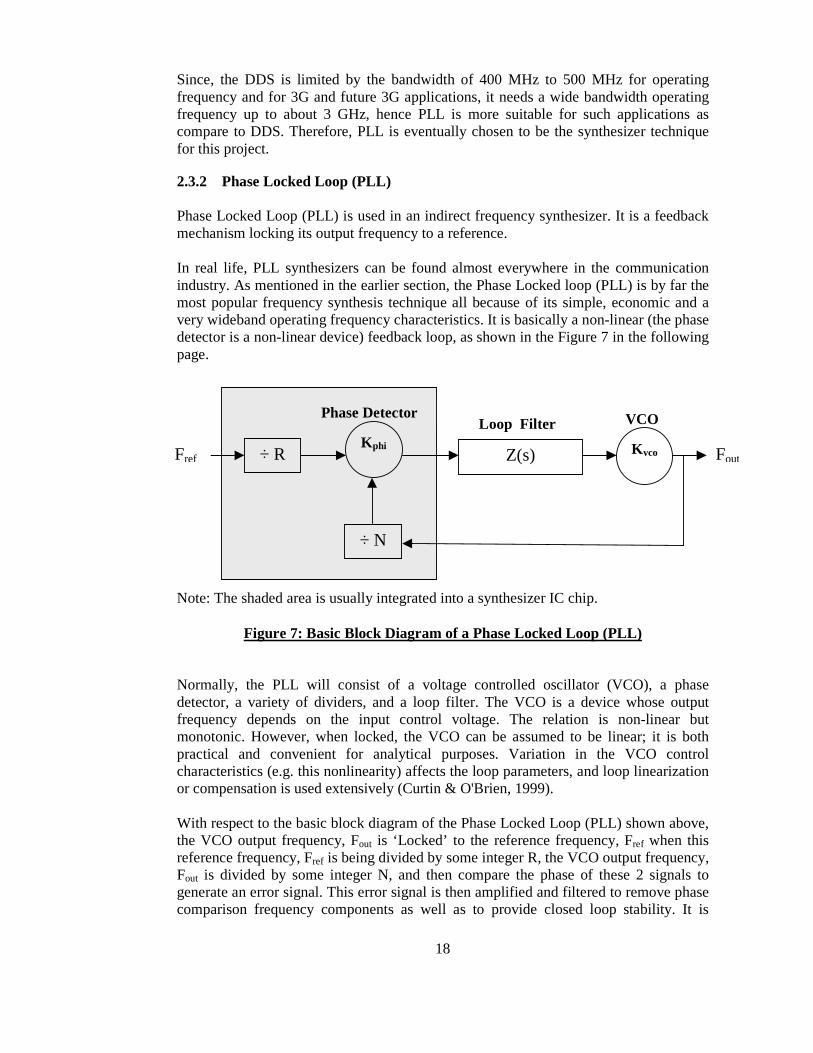
Since, the DDS is limited by the bandwidth of 400 MHz to 500 MHz for operating frequency and for 3G and future 3G applications, it needs a wide bandwidth operating frequency up to about 3 GHz, hence PLL is more suitable for such applications as compare to DDS. Therefore, PLL is eventually chosen to be the synthesizer technique for this project.
2.3.2 Phase Locked Loop (PLL)
Phase Locked Loop (PLL) is used in an indirect frequency synthesizer. It is a feedback mechanism locking its output frequency to a reference.
In real life, PLL synthesizers can be found almost everywhere in the communication industry. As mentioned in the earlier section, the Phase Locked loop (PLL) is by far the most popular frequency synthesis technique all because of its simple, economic and a very wideband operating frequency characteristics. It is basically a non-linear (the phase detector is a non-linear device) feedback loop, as shown in the Figure 7 in the following page.
Note: The shaded area is usually integrated into a synthesizer IC chip.
Figure 7: Basic Block Diagram of a Phase Locked Loop (PLL) Normally, the PLL will consist of a voltage controlled oscillator (VCO), a phase detector, a variety of dividers, and a loop filter. The VCO is a device whose output frequency depends on the input control voltage. The relation is non-linear but monotonic. However, when locked, the VCO can be assumed to be linear; it is both practical and convenient for analytical purposes. Variation in the VCO control characteristics (e.g. this nonlinearity) affects the loop parameters, and loop linearization or compensation is used extensively (Curtin & O'Brien, 1999). With respect to the basic block diagram of the Phase Locked Loop (PLL) shown above, the VCO output frequency, Fout is ‘Locked’ to the reference frequency, Fref when this reference frequency, Fref is being divided by some integer R, the VCO output frequency, Fout is divided by some integer N, and then compare the phase of these 2 signals to generate an error signal. This error signal is then amplified and filtered to remove phase comparison frequency components as well as to provide closed loop stability. It is
Z(s)
÷ N
VCO
Fout
Phase Detector
Fref ÷ R K phi
Loop Filter
K vco

19
almost always the case that the reference frequency, Fref is a higher quality frequency source than the VCO output frequency, Fout. Like any other engineering product, a frequency synthesizer (FS) needs to meet a set of specifications or parameters. A list of major synthesizer parameters that are important to this project are illustrated as below (Egan, 1990).
Frequency Range
This specifies the output frequency range, including the lower and higher frequencies that can be obtained from the frequency synthesizer. The units of frequency are hertz (Hz), or cycles per second.
Frequency Resolution
This parameter is also referred to as the step size, and it specifies the minimum step size of the frequency increments. For example, if a frequency synthesizer covers a frequency range from 1.5 GHz to 3 GHz and has a step size of 100 Hz; it is capable of generating any frequency between 1.5 GHz to 3 GHz in 100 Hz steps. In many applications, the step size is not fixed. This happens when a part of the synthesizer is generated by dividing a fixed frequency with a range of numbers.
Channel Spacing
This specifies the amount of bandwidth allocated to each channel in a communications system that transmits multiple frequencies such as the frequency synthesizer. It is measured as the spacing between center frequencies (or wavelengths) of adjacent channels.
Phase Noise at a Specific Offset from the Output
For a carrier frequency at a given power level, the phase noise of a synthesizer is the ratio of the carrier power to the power found in a 1-Hz bandwidth at a defined frequency offset (usually 1 KHz for a synthesizer). Expressed in dBc/Hz, the in-band (or close-in) phase noise is dominated by the synthesizer; the VCO noise contribution is high-pass filtered in the closed loop.
Acquisition/Lock Time after Switching to a New Frequency (to get within one cycle slip of new frequency)
This refers to the period of time required to attain synchronism in the frequency synthesizer especially after switching from one specified frequency to another new frequency in order to get within one cycle slip of new frequency.
Settling/Lock Time (for phase error to decrease from near 360 degrees to near zero)
This refers to the time it takes for phase error to decrease from near 360 degrees to near zero. The time required for an amplifier, relays, or other circuits to reach a stable mode of operation. In general, settling time for full-scale step refers to the amount of time

20
required for a signal to reach certain accuracy and stay within that range of accuracy. Settling time can be a major source of error for multichannel acquisition systems because the switching between channels can cause large voltage steps that the instrumentation amplifier may not be able to track quickly.
Switching Time
This parameter specifies the speed whereby the frequency synthesizer can hop from one specified frequency to another specified frequency within a given frequency tolerance. There are many definitions for this parameter. In some applications, the requirement is to settle to within a specific frequency from the desired new frequency (e.g. 10 Hz or 1 KHz from the desired frequency). Another more common but more demanding specification that defines the switching speed is by the time it takes the output phase to settle to 0.1 radian of the final phase.
Spurious Signal Level
Overmodulation on the signal will results in spurious signal created and the level of such unwanted spurious signal is called the spurious signal level. Active RF and microwave systems frequently generate non-harmonically related signals that need to be identified and measured. Tracking down and then reducing the level of unwanted spurious signals can be done by using a spectrum analyser.
Power Consumption/Dissipation
This refers to the electrical energy over time that must be supplied to the frequency synthesizer so as to maintain its operation. The power consumption is usually a result of power used to perform the intended function of the device plus additional "wasted" power that is dissipated as heat and/or light. On the other hand, power dissipation is the transference of heat generated by the device during normal operation. Both the power consumption and power dissipation is usually measured in units of watts. First of all, in order to look for a suitable frequency synthesizer evaluation board for measurement and comparison to current 3G and predicted future 3G synthesizer design, there is a need to search for all those important parameters of the current 3G radio system that are mentioned above. Unfortunately, not all of these important parameters on the current 3G radio systems are found. Only some of the typical values of these parameters that are being used currently in 3G systems are found to compare to the specifications of the evaluation boards available in the market. A survey on the available frequency synthesizer evaluation boards from different manufacturers such as Analog Devices, National Semiconductor, Texas Instruments and etc is also being conducted in the starting phase of this project. Having the constraints of the budget allocated as well as the suitable 3G specifications required, there are only a total of 6 potential frequency synthesizer evaluation boards that are available and suitable for this project. Some of the performance and technical details of these 6 potential frequency synthesizer evaluation boards are being captured in a table for easy comparison in the next section as shown in the following page.

21
2.4 Comparative Analysis on Frequency Synthesizer Evaluation Boards
For comparative analysis on these 6 different frequency synthesizer evaluation boards available in the market, a comparison table had been drawn up as shown below.
Table 4: Different Frequency Synthesizer Evaluation Board Comparison Table
Manufacturer Analog Devices National Semiconductor Texas
Instrument Singapore
Technologies Model No ADF4360-1 ADF4360-0 LMX2310U LMX2347 TRF3761 STW81100 Price US$120 US$120 US$147 US$147 Not Indicated Not Indicated Integrated VCO Yes Yes No No Yes Yes Operating Frequency Range
2.05 GHz to 2.45 GHz
2.4 GHz to 2.725 GHz
2.5 GHz 2.5 GHz 375 MHz to 2.4
GHz 825 MHz to 4.4
GHz Data to Clock Set Up Time
10 ns (Min) 10 ns (Min) 50 ns (Min) 50 ns (Min) 10 ns (Min) 2 ns (Min)
Data to Clock Hold Time
10 ns (Min) 10 ns (Min) 20 ns (Min) 10 ns (Min) 10 ns (Min) 2 ns (Min)
Clock Pulse Width High
25 ns (Min) 25 ns (Min) 50 ns (Min) 50 ns (Min) 50 ns (Min) 10 ns (Min)
Clock Pulse Width Low
25 ns (Min) 25 ns (Min) 50 ns (Min) 50 ns (Min) 50 ns (Min) 5 ns (Min)
Lock Time/ Switching Time
400 µs (Typ) 250 µs (Typ) 500 µs (Typ) 450 µs (Typ) 300 µs (Typ) 150 µs (Typ)
VCO Phase-Noise Performance
-148 dBc/Hz (Typ) at 10 MHz
offset from carrier
-145 dBc/Hz (Typ) at 10 MHz
offset from carrier
N.A. N.A.
-160 dBc/Hz (Typ) at 10 MHz
offset from carrier
-148 dBc/Hz (Typ) at 10 MHz
offset from carrier
In-Band Phase Noise
-81 dBc/Hz (Typ) at 1 KHz
offset from carrier
-80 dBc/Hz (Typ) at 1 KHz
offset from carrier
-76 dBc/Hz (Typ) at 1 KHz
offset from carrier
-83 dBc/Hz (Typ) at 1 KHz
offset from carrier
-84 dBc/Hz (Typ) at 1 KHz
offset from carrier
-56 dBc/Hz (Typ) at 1 KHz
offset from carrier
Software for the board
More user-friendly
More user-friendly
Less user-friendly
Less user-friendly
Did not look into it
Did not look into it

22
From the specifications of each evaluation boards, the STW81100 multi band RF frequency synthesizer evaluation board from Singapore Technologies actually has the better performance over the others due to its wide coverage range of operating frequency from 825 MHz to 4.4 GHz and other performance factors. Unfortunately, there is no price indication for it hence, it is not chosen. Since there is also no price indication for the TRF3761 from Texas Instruments, the final choice are being left with either the frequency synthesizer evaluation board from Analog Devices or National Semiconductor. From performance wise, both the ADF4360-1 and ADF4360-0 from Analog Devices is indeed better than both the LMX2310U and LMX2347 from National Semiconductor. They are also slightly less expensive in price as compared to the LMX2310U and LMX2347. Moreover, both the ADF4360-1 and ADF4360-0 from Analog Devices had integrated VCO (unlike the LMX2310U and LMX2347 from National Semiconductor) that allows user to measure the inputs and outputs from this VCO. On top of that, the user-friendliness and the effectiveness of the software available to drive both the evaluation boards from Analog Devices and National Semiconductor are also being considered. Firstly, the evaluation board software from Analog Devices and National Semiconductor are being downloaded from respective website for testing out on their usage and user-friendliness. There are a total of 2 types of software available on the Analog Devices website. They are the ADIsimPLL v.3.0 software and the ADF4360 evaluation board programmable software. The ADIsimPLL is actually a PLL Circuit Design and Virtual Evaluation Software. It can be considered as a simulation tool and thus there is no need to connect the evaluation board in order to use this software. This ADIsimPLL software supports a wide range of devices from Analog Devices. By choosing the PLL chip to be ADF4360-1 and following the steps given in the software, a series of output results such as frequency and time domain graphs and etc will be generated out automatically. Appendix F of this dissertation displays an example on these output results generated by ADIsimPLL v.3.0 software. As for the ADF4360 evaluation board programmable software, from the first tried out, it seems to be an evaluation tool for user to set up the data for the registers and other settings, and then program them into the evaluation board for it to run. However, further investigations on how and where the evaluation board can be connected to a computer running this software are still required. This software is mainly being used by the ADF4360 series of devices. In short, this software still needs sometime and experiment on it before we finally understand what it can actually do. The main interface page of the ADF4360 evaluation board programmable software is being reflected as Figure 10 under Section 3.3 in this dissertation. On the other hand, there are also a total of 2 types of software available on the National Semiconductor website. They are the Code Loader v.2.2.0 software and the Easy PLL software. The Code Loader software needs to setup the port settings and connections to the evaluation board via the computer parallel port. Similar to the ADF4360 evaluation board programmable software, it is consider as programmable software that uploads data for the register into the evaluation board for it to run. An example of the Port Setup tab and the PLL tab of this Code Loader software are being captured as Appendix G and H respectively in this dissertation.

23
Finally, for the EasyPLL software, it can be consider as online simulation software. Unfortunately, it seems like there is no selection for LMX2310U PLL in this software. Only LMX2347 PLL can be chosen in this software. Hence, it is not suitable to be use to simulate the performance for the LMX2310U evaluation board. After the first attempt in trying out to see which software is more easy to be use, ADIsimPLL software v.3.0 seems to be more user-friendly and is able to generate better output results when compare to EasyPLL and Code Loader. However, both the ADIsimPLL v.3.0 and the ADF4360 evaluation board programmable software still requires further investigation and experiment on it before we can finally draw a conclusion on what is their actual usage. As per now, ADIsimPLL software v.3.0 maybe consider as a suitable software that can stimulate and cross check all measurements or findings being done physically on the evaluation board. From all the performance and the software findings mentioned above, it is no doubt that Analog Devices evaluation boards are slightly better than those from National Semiconductor. Therefore, the idea of choosing either the LMX2310U or LMX2347 evaluation boards from National Semiconductor had been dropped. Finally, it left only the ADF4360-1 and ADF4360-0 evaluation board to choose from. Since the operating output frequency range for ADF4360-1 is from 2.05 GHz to 2.45 GHz, which is very close to the predicted future 3G operating frequency range of 2.3 GHz to 2.5 GHz and its performance are very similar to ADF4360-0, ADF4360-1 is finally selected to be use for this project. This ADF4360-1 is a fully integrated integer-N synthesizer and VCO that is suitable for 3G WCDMA systems applications.

24
3. EVALUATION BOARD
3.1 Description on Evaluation Board
The ADF4360-1 evaluation board (EVAL-ADF4360-1EB1) from Analog Devices is designed to allow user to evaluate the performance of the ADF4360-1 Frequency Synthesizer consisting of an integrated Phase Locked Loop (PLL) and a Voltage Controlled Oscillator (VCO). This ADF4360-1 evaluation board mainly consists of the following important items inside it. They are:
i) ADF4360-1 Synthesizer Integrated Circuit (IC) Chip ii) TCX010 External Reference Oscillator iii) Power On/Off Switch iv) Battery Compartment v) RF Output A & B (Sub-Miniature Type-A “SMA” Female Plug) vi) Serial Port (9-Pin Personal Computer Male Connector)
Apart from those important items mentioned above, unpopulated SMA footprints are also made available for the power supplies, Chip Enable (CE) and external reference input. It also contains a loop filter to complete the PLL. This board can be modified as necessary for the customers PLL requirements. A cable is included with the board for connection to a Personal Computer (PC) parallel port to allow software programming on the registers. Section 3.3 will elaborate more on this software programmability part. A picture of the ADF4360-1 evaluation board is captured as Figure 8 as shown below.
Figure 8: Picture of the ADF4360-1 Evaluation Board
TCX010 External Reference Oscillator
ADF4360-1 Synthesizer IC Chip
RF Output A & B (“SMA” Female Plug)
Serial Port (9-Pin PC Male Connector)
Power On/Off Switch
Battery Compartment

25
This evaluation board is powered from a single 9V battery. All components necessary for Local Oscillator (LO) generation are catered for on-board. The 10 MHz TCX010 external reference oscillator provides the necessary input reference frequency to the ADF4360-1 Synthesizer IC Chip. The ADF4360-1 Synthesizer IC Chip consists of a fully integrated integer-N synthesizer and Voltage Controlled Oscillator (VCO). The ADF4360-1 is designed for a center frequency of 2.25 GHz. In addition, there is a divide-by-2 option available, whereby the user gets a Radio Frequency (RF) output of between 1025 MHz and 1225 MHz. Control of all the on-chip registers is through a simple 3-wire interface. The device operates with a power supply ranging from 3.0 V to 3.6 V and can be powered down when not in use. The following page shows the functional block diagram of this ADF4360-1 Synthesizer IC Chip which is already soldered mount onto the ADF4360-1 evaluation board.
Figure 9: Functional Block Diagram of ADF4360-1 Synthesizer IC Chip inside the
Evaluation Board Basically, the ADF4360-1 Synthesizer IC Chip operates very similar to Figure 7, the basic block diagram of the Phase Locked Loop (PLL) shown in Section 2.3.2. With respect to the functional block diagram shown above, similarly, there will be an input reference frequency coming from the TCX010 external reference oscillator into the circuit (in this case it is going into the REFIN node), this reference frequency will then need to pass through the 14-Bit R Counter which will then divide this reference

26
frequency to produce the reference clock to the Phase Frequency Detector (PFD) frequency or the channel spacing. Finally, it is then applied to one of input to the Phase Comparator or the Phase Detector. Depending on the type of PLL design created by the user, the integer R or the division ratio, R that is allowed in this evaluation board ranges from 1 to 16,383. In this project, the division ratio, R is set at 2 since the Phase Frequency Detector (PFD) frequency or the channel spacing required for this PLL design is agreed to be at 5 MHz. By dividing the input reference frequency of 10 MHz by 2 (using the division ratio, R), it is able to produce a channel spacing of 5 MHz. On the other hand, the clock from the VCO will need to go through the Multiplexer and then the Dual-Modulus Pre-Scaler (P/P + 1), which divides it down to a manageable frequency for entering into the Complementary Metal Oxide Semiconductor (CMOS) A and B Counters. This Dual-Modulus Pre-Scaler, along with the A and B Counters, enables a large division ratio, N in the PLL feedback counter. This division ratio, N is actually equals to (BP + A). There is a minimum divide ratio possible for fully contiguous VCO output frequencies and this minimum is determined by P, which is the pre-scaler value given by the formula (P2 – P). The A and B Counters (which is the 18-Bit N Counter), in conjunction with the Dual-Modulus Pre-Scaler, make it possible to generate VCO output frequencies that are spaced only by the reference frequency divided by Integer R. Finally, the output from both the A and B Counters is then applied to the other input pin to the Phase Comparator. Following next, the output from the Phase Comparator will then goes into the Charge Pump (CP), whose output point is in fact the input point for the external loop filter (not shown in the functional block diagram of Figure 9). The output of the Phase Comparator mainly consists of pulses whose length depends linearly on the phase difference between the two inputs. These pulses will then activate the charge pump, which eventually drives the external loop filter connected between the Charge Pump (CP) pin and the VTUNE pin. Generally, this external loop filter connected between the Charge Pump (CP) pin and the VTUNE pin, can either be the standard third order passive loop filter or the third order active loop filter that was normally used if the tuning voltage required for the VCO is higher than the output range of the synthesizer charge-pump. For this project, the type of loop filter configuration chosen is the Charge Pump Passive 2 Capacitors type. When the Charge Pump (CP) output is enabled, the current pulses from the charge pump output are then filtered by this external loop filter to become a voltage, which in turn drives the tuning port of the internal VCO. Next, from the output of the loop filter, it will go to VTUNE pin that acts as the control input to the VCO, which is at the VCO CORE module. This voltage determines the output frequency and is derived from filtering the CP output voltage. Finally, the VCO output frequency will come out from the OUTPUT STAGE module, and then to the RFOUTA and RFOUTB SMA female plug. The output level of the RFOUTA and RFOUTB is programmable from -6 dBm to -13 dBm. It is note that the register and latch settings for the 14-Bit R Counter, the 24-Bit Function Latch and the 13-Bit B Counter and 5-Bit A Counter (which forms the 18-Bit

27
N Counter) will need to be set by the user using the ADF4360 evaluation board programmable software that comes along with the evaluation board.
3.2 Capabilities of the Evaluation Board
The features of this ADF4360-1 evaluation board are reflected in the table shown below.
Self contained board for generating RF frequencies
Flexibility for reference input, PFD frequency and loop bandwidth
Output frequency range of 2.05 GHz to 2.45 GHz
Accompanying software allows complete control of synthesizer functions from PC
Battery operated: 9V supplies Analog and digital lock detect Typical phase noise performance of -140
dBc / Hz at 3 MHz offset Typical spurious performance of -70 dBc
at 200 KHz offset, (2.25 GHz Output)
Table 5: Features of ADF4360-1 Evaluation Board Some applications of this ADF4360-1 evaluation board include:
i. Wireless handsets (DECT, GSM, WCDMA) ii. Test equipment iii. Wireless LANs iv. CATV equipment
On top of that, the ADF4360-1 evaluation board can also be used as a local oscillator for a direct conversion modulator that had been increasingly being used to implement base station transmitters. Other applications for this evaluation board can be found at the end of the ADF4360-1 data sheet.
3.3 ADF4360 Evaluation Board Programmable Software
The ADF4360-1 digital section includes a 24-bit input shift register, a 14-bit R counter, and an 18-bit N counter, comprising of a 5-bit A counter and a 13-bit B counter. Data is clocked into the 24-bit shift register on each rising edge of the serial clock input (CLK). The data is clocked in Most Significant Bit (MSB) first. When the Load Enable (LE), goes high, the data stored in the shift registers is loaded into one of the four latches, and the relevant latch is selected using the control bits. Basically, the destination latch is being determined by the state of the two control bits (C2, C1) in the shift register. The truth table for these bits is shown in Table 6 on the following page. Note that the test mode latch is only used for factory testing and therefore it should not be programmed by the user.

28
Table 6: Truth Table for Control Bits C2 and C1
In order to measure the respective parameters in the evaluation board such as the Lock Time, VCO Output Frequency and etc, the registers for the R Counter, Control Latch and N Counter needs to be programmed first by the user using the ADF4360 evaluation board programmable software. A screenshot of the Main Interface Page of this ADF4360 evaluation board programmable software is shown below as Figure 10.
Figure 10: Main Interface Page of the ADF4360 Evaluation Board Programmable Software
Some standard steps for using this ADF4360 evaluation board programmable software are shown below. Steps:
i) Install ADF4360.exe evaluation board programmable software (version REV 2.0) into a computer or a laptop that have a parallel port.
ii) Connect the ADF4360-1 evaluation board to this computer via the 9 Female D-Type to 25 Male D-Type PC cable that comes with the evaluation board.
Control Bits Data Latch C2 C1
Control Latch 0 0 R Counter 1 1 N Counter (A and B Counters) 1 0 Test Mode Latch 1 1

29
iii) Insert a 9V battery into the ADF4360-1 evaluation board and power it up using the Power On/Off switch on the evaluation board.
iv) Run the ADF4360.exe evaluation board programmable software (version REV 2.0).
v) Start the programming of registers and other settings. Before programming the registers for the respective counters or latches, it is always a good practice to first check on the connections (from the evaluation board to the computer parallel port) to see if they are correctly secure or to check if the programmable software is working fine or not (as if programmed of register is working fine or not). To check on these 2 points, the following intialisation steps need to be performed. Steps:
i) Check if the red LED (D4) lights up when applying the power to the evaluation board by switching the Power On/Off switch to on.
ii) Run the programmable software and select ADF4360-1 as the desired device.
iii) Click on the “Muxout” button shown on the Main Interface Page. iv) Select to program “DVdd” and load it by pressing “Load Now” button
once. If the green LED (D1) on the board attached to this pin lights up, it means the user is programming the part correctly and shows that the connection is secure.
v) Now, select to program “Digital Lock Detect”, press “Load Now” button once followed by pressing “OK” button once.
vi) Then, click on “RF PD Polarity Positive” button shown on the Main Interface Page (refer to Figure 10) to “RF PD Polarity Negative” and back (make sure it is finally at positive). With the RF PD Polarity bit set to positive, it will ensure that all registers are loaded. If the green LED (D1) is still lighted up, then an output frequency of 2400 MHz should be seen on the spectrum analyzer when the spectrum analyzer is connected to the point, RFOUTA.
By selecting the ADF4360-1 device as the desired device to program the register, the software will automatically display the desired RF VCO output frequency as 2400 MHz, the PFD frequency as 200 KHz and the REF IN frequency as 10 MHz. Generally, for an Integer-N PLL, the Phase Frequency Detector (PFD) frequency is equal to the step size, which is also equal to the channel spacing as well as the Phase Detector Frequency (PDF). A screenshot on the “Muxout Options” menu with respect to the steps mentioned above is shown as Figure 11 on the following page. The word, “Digital Lock Detect” is being circle in red so as to highlight that the software is now programming the Muxout feature, “Digital Lock Detect”. If the above-mentioned steps are completed and have the same results as mentioned, it means that the connections are correctly secure and the programmable software is working fine. User can now proceed to change the other parameters or set the registers as they wish.
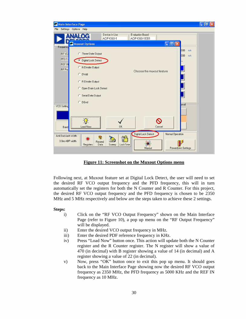
30
Figure 11: Screenshot on the Muxout Options menu
Following next, at Muxout feature set at Digital Lock Detect, the user will need to set the desired RF VCO output frequency and the PFD frequency, this will in turn automatically set the registers for both the N Counter and R Counter. For this project, the desired RF VCO output frequency and the PFD frequency is chosen to be 2350 MHz and 5 MHz respectively and below are the steps taken to achieve these 2 settings.
Steps:
i) Click on the “RF VCO Output Frequency” shown on the Main Interface Page (refer to Figure 10), a pop up menu on the “RF Output Frequency” will be displayed.
ii) Enter the desired VCO output frequency in MHz. iii) Enter the desired PDF reference frequency in KHz. iv) Press “Load Now” button once. This action will update both the N Counter
register and the R Counter register. The N register will show a value of 470 (in decimal) with B register showing a value of 14 (in decimal) and A register showing a value of 22 (in decimal).
v) Now, press “OK” button once to exit this pop up menu. It should goes back to the Main Interface Page showing now the desired RF VCO output frequency as 2350 MHz, the PFD frequency as 5000 KHz and the REF IN frequency as 10 MHz.

31
A screenshot on the “RF Output Frequency” pop up menu with respect to the steps mentioned above is shown as Figure 12 below. The values for the desired RF VCO output frequency, PDF frequency and the respective registers are being circle in red so as to highlight the new settings set by the user.
Figure 12: Screenshot on the RF Output Frequency menu Note that the “Load Now” and “OK” button will only update the N register and R Register for the N Counter and R Counter respectively. If the user changes only the VCO output frequency, then only the N register will be updated. If the user changes only the PFD reference frequency, then only the R register will be updated. If the user changes both the VCO output frequency and the PFD reference frequency, then both the N register and R register will be updated. Now, in order to see what are the exactly bits settings from Least Significant Bit (LSB) to Most Significant Bit (MSB) for the control latch, N register and R register, user can press on the “Registers” button shown on the Main Interface Page (refer to Figure 10). This “Registers” button is useful as it can show the user the three registers settings at once. The user can simply see these settings by just pressing the updates button for each of the register. A screenshot on the “Registers” menu is shown as Figure 13 below. To highlight the values (in hexadecimal) written for each register, they are being circle in red in the figure shown below.

32
Figure 13: Screenshot on the Registers menu By pressing the “Load Now” button as shown in the Registers menu seen above, it will load these updated register settings into the registers. The correct sequence of register writes is to the R Counter, the Control Latch and finally the N Counter. In general, this ADF4360 evaluation board programmable software is not an intelligent software. It simply programs the registers whenever the user instructs it to do it. It does not monitor the part to see if it is actually at the desired frequency or not. It is just a simple Graphic User Interface (GUI) software to help user to program the registers.
3.4 Measurements and Difficulties Encountered
One of the tasks for this project is to measure the parameters and performance of this ADF4360-1 frequency synthesizer evaluation board with respect to the following parameters that are important for future 3G applications.
i) Channel Spacing ii) VCO Inputs and Outputs iii) Filter Outputs iv) Lock Time (Frequency & Phase) v) Phase Noise
First of all, in order to familiarize with the ADF4360-1 evaluation board, measuring all the test points that are already made available on the evaluation board itself had been

33
carried out. There are a total of 11 test points excluding Test Point T4, which is the ground point for the evaluation board. All these measurements are measured without knowing the fact that the registers for the R Counter, Control Latch and N Counter needs to be programmed first using the ADF4360 evaluation board programmable software that comes with the board. Before moving directly to measure all the test points, in order to prevent Electro Static Discharge (ESD) from my body into the evaluation board and eventually damage the board, an ESD or an anti-static wrist straps was specially bought to combat the static build up on my body. By using this ESD wrist strap, it will ensure that any charge built up on a person working on this evaluation board is safely dissipated. An ESD wrist strap consists of two sections. First of all, the band itself, which is worn around the wrist. This is connected to earth via the lead, which incorporates a large value resistor, normally in excess of 1 Mega Ohm. This is included for two reasons. The first is safety, and the second is again to ensure that any static is removed in a controlled fashion. Normally, the ESD wrist straps should be regularly tested to ensure they have not become open circuit. Without a test of this nature, a faulty strap could go undetected for many months. Many companies insist that every strap that is in use is tested every day. In this way any defects can be discovered early before they cause too much damage on the electronic components or circuits (Radio Electronics, 2006).
ESD wrist straps, connections to workbench tops and any other points are normally connected together using a special junction box. These junction boxes usually have resistors of 1 Mega Ohm for each of the contacts. These are joined and then taken to earth. Often a special mains plug with a connection to only the earth pin can be used. These special plugs are usually yellow and have two plastic pins for the live and neutral, and a metal pin for the earth. In this way it is only possible to connect to earth. A picture of this ESD wrist strap is shown below as Figure 14.
Figure 14: Picture on the ESD Wrist Strap At the same, in order to measure the output frequency response from RFOUTA and RFOUTB SMA female plug, there is need to look for a suitable connector available for connecting the RFOUTA and RFOUTB SMA female plug on the evaluation board to a 3 GHz spectrum analyzer. Since there isn’t any suitable connector available in my workplace hence, a trip down to Sim Lim Tower was made to look for one that is

34
suitable. After visiting a few different electrical component stores, 2 suitable Sub-Miniature Type-A (SMA) Male plug to Bayonet Neill Concellman (BNC) Female jack connector from one of the electrical component store had been finally found and bought for the project. A picture of this SMA Male plug to BNC Female jack connector that had been bought for this project is shown below as Figure 15. To facilitate the connections, a 50 Ohm (RG 58) BNC (Male to Male) cable was also made available from my workplace.
Figure 15: Picture on the SMA Male Plug to BNC Female Jack Connector The high speed oscilloscope that was being used for the first measurements on all the test points is the Tektronix TDS3014B high speed oscilloscope, with the specifications of 100MHz (1.25GS/s) and the probe used here is of 10 MHz bandwidth. A picture of this Tektronix TDS3014B high speed oscilloscope is shown below as Figure 16.
Figure 16: Picture on the Tektronix TDS3014B High Speed Oscilloscope The first measurements are being carried out simply by powering up the evaluation board and connecting the probe from Channel 1 of the high speed oscilloscope to the respective test points with the ground pin of the probe connected to Test Point, T4 (which is the ground point for the evaluation board). The output results and the output waveforms for the Test Point, T1 and T2 will be discuss later in Chapter 5. From the first measurements, the measurement results seem to be a bit strange and incorrect as most of the other test points have some sort of a DC straight line output waveforms. Therefore, in order to verify and make sure what had been measured so far

35
are actually correct, a second round of measurements on all the test points using another high speed oscilloscope had been carried out. The high speed oscilloscope that was being used this time for the second measurements on all the test points is the LeCroy Wave Surfer 424, with the specifications of 200 MHz (2GS/s). The probe used here is of 200 MHz bandwidth. A picture of this LeCroy Wave Surfer 424 high speed oscilloscope is shown below as Figure 17.
Figure 17: Picture on the LeCroy Wave Surfer 424 High Speed Oscilloscope The output results for these second measurements will also be discussed later in Chapter 5. With this second round of measurements, it had proved that the measured values in the first round of measurements should be correct, however the values and the output waveforms for the other 9 test points still seem to be incorrect. After checking these measurement results with the Applications Engineer from Analog Devices, it was realized that there is a need to program the registers for the R Counter, Control Latch and N Counter first using the ADF4360 evaluation board programmable software before starting to measure all the test points and the parameters on the board that are required for future 3G applications. After realizing this point from the Analog Devices Applications Engineer, it shows that what had been measured before are not the correct output results. In order to know how to program those registers for the R Counter, Control Latch and N Counter using the ADF4360 evaluation board programmable software, some hands on session on this software using a trial and error method had been performed. However, a lot of problems were encountered when using this ADF4360 evaluation board programmable software.

36
The only way to overcome all these problems faced is to read through all the required information and data sheets for this evaluation board in details and tries to understand them since there is no instructions booklet for this programmable software inside the evaluation board package. Problems encountered that still have not been resolved by end of Wk 631 (which is by end of first week of August 2006) even with the advice from the Application Engineer from Analog Devices, were also highlighted to the project supervisor. Without having to resolve all the problems faced in using the ADF4360 evaluation board programmable software, a limitation of the ADF4360-1 evaluation board had been found out from the Application Engineer from Analog Devices. This limitation is that the evaluation board will not remember the registers programmed after it have been powered down. This ADF4360-1 evaluation board does not have a memory cache or a memory location to store/save the register settings that had been programmed into the evaluation board before it is power off. In other words, it will not remember the previous settings that had been programmed to the registers after power off and user will need to re-program the registers all over again after power up. With this limitation on the ADF4360-1 evaluation board, it leads to another problem. The problem is that, now there is a need to install the ADF4360 evaluation board programmable software in my workplace computer since all the measuring equipment that are required for this project are all from my workplace. However, in order to install any new software into my workplace computer, it is necessary to request for administrator rights from my company. Unfortunately, as this software is not meant to be used for work purposes, the administrator rights for installing this software were not approved. Therefore, it is required to look for other alternatives to resolve this issue. Another alternative that had been taken is to install the ADF4360 evaluation board programmable software into my laptop. By installing the software into my laptop allows me to have the flexibility to bring my laptop to my workplace any day whenever there is a need to program the registers for measurement. However, since my laptop does not have a standard parallel port built in, I had to think of other means to create a standard parallel port out from the other output ports such as the Universal Serial Bus (USB) port in my laptop. After doing some research on that via Internet, a USB to 25-Pin Female (Parallel) adaptor cable had been bought for connecting my laptop to the evaluation board. Unfortunately, the outcome is not feasible and thus leads me to search for another alternative. A picture of the USB to 25-Pin Female (Parallel) adaptor cable that had been bought for this project is shown as Figure 18 on the following page.
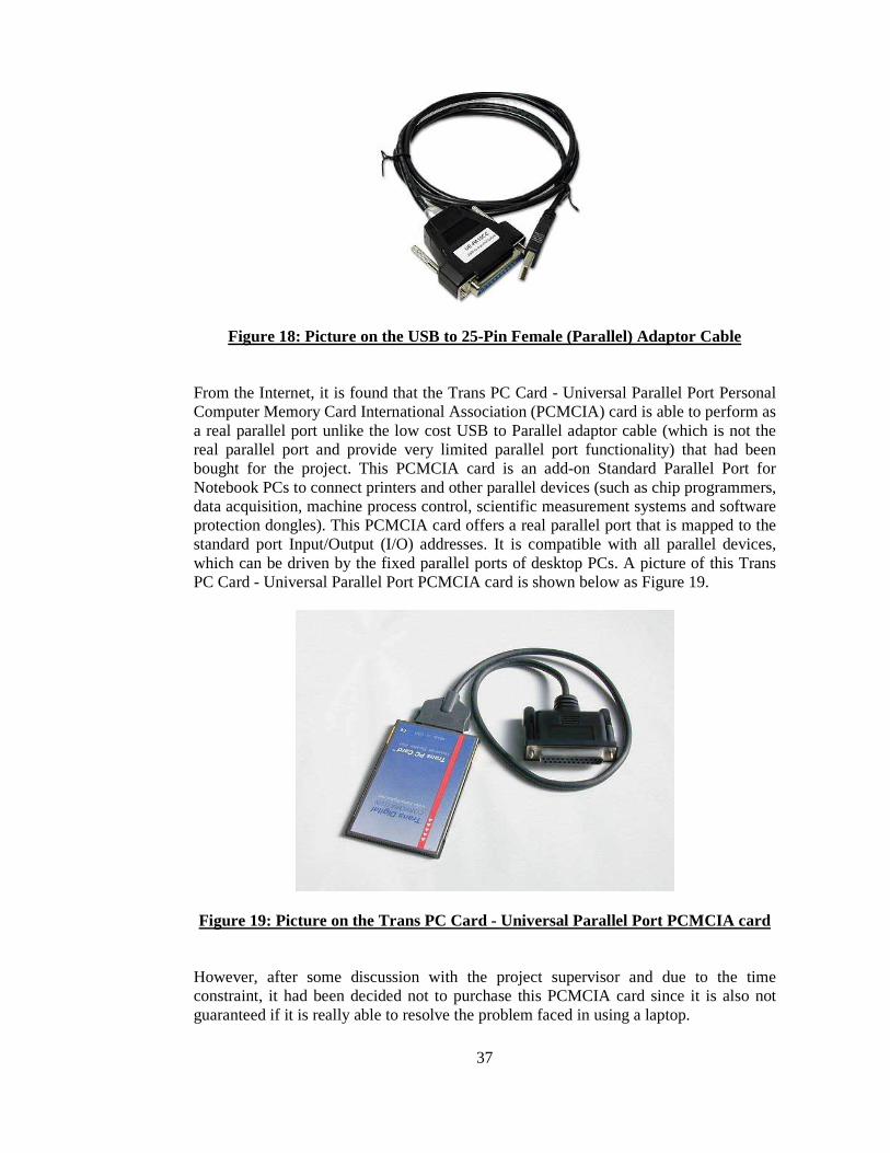
37
Figure 18: Picture on the USB to 25-Pin Female (Parallel) Adaptor Cable From the Internet, it is found that the Trans PC Card - Universal Parallel Port Personal Computer Memory Card International Association (PCMCIA) card is able to perform as a real parallel port unlike the low cost USB to Parallel adaptor cable (which is not the real parallel port and provide very limited parallel port functionality) that had been bought for the project. This PCMCIA card is an add-on Standard Parallel Port for Notebook PCs to connect printers and other parallel devices (such as chip programmers, data acquisition, machine process control, scientific measurement systems and software protection dongles). This PCMCIA card offers a real parallel port that is mapped to the standard port Input/Output (I/O) addresses. It is compatible with all parallel devices, which can be driven by the fixed parallel ports of desktop PCs. A picture of this Trans PC Card - Universal Parallel Port PCMCIA card is shown below as Figure 19.
Figure 19: Picture on the Trans PC Card - Universal Parallel Port PCMCIA card
However, after some discussion with the project supervisor and due to the time constraint, it had been decided not to purchase this PCMCIA card since it is also not guaranteed if it is really able to resolve the problem faced in using a laptop.

38
Another problem that was encountered in the project is the difficulties in accessing the 3 GHz spectrum analyser for the measurement of the output frequency response from the evaluation board. As there is only one 3 GHz spectrum analyser in my workplace, getting access to it seems to be really difficult even though I had already convinced the person who have the access to it to lend it to me after work. The common problem that I had faced is either the person who had access to the 3 GHz spectrum analyzer is not around in my workplace when I need to borrow it or this 3 GHz spectrum analyzer had been used for overnight testing. On top of all the problems and difficulties that I had faced throughout the project phase, the workload given to me by my company sometimes also refrained me from carrying out such measurements after work. With all these difficulties and problems encountered, it resulted in not able to carry out the measurements on the evaluation board as planned. Furthermore, due to the time limit and the fact that it is really difficult to get the access to the 3 GHz spectrum analyser for measuring the requirements or parameters that are needed for 3G and future 3G applications, these measurements are being supplemented by using simulation software from Analog Devices, called the ADIsimPLL.

39
4. SIMULATION SOFTWARE
4.1 Description on Simulation Software
ADIsimPLL is a simulation software that had been developed by engineers for engineers for the sole purpose of optimizing Phase Locked Loop (PLL) designs, making it faster and easier for any user to accomplish his/her individual goals. This simulation software enables the rapid and reliable evaluation of new high performance PLL products from Analog Devices. It is the most comprehensive PLL Synthesizer design and simulation tool available today. Simulations performed include all key non-linear effects that are significant in affecting PLL performance. From the entry-level engineer to the seasoned veteran, ADIsimPLL has an arsenal of onboard tools and options that are guaranteed to maximize the efficiency of the user’s circuit design. In general, the ADIsimPLL is the easy way to design, analyse and simulate PLL frequency synthesizers using the ADF4000 range of PLL IC’s from Analog Devices. With its superior functionality, unlimited flexibility, and user-friendly interface, it allows user to analyse the performance (including phase noise, transient response, and lock time to frequency or phase tolerances). Currently, the latest version of this ADIsimPLL simulation software is 3.0 and it can be downloaded from the Analog Devices homepage.
4.2 Functions of ADIsimPLL
First of all, in order to get to know the functions and the capabilities of what the ADIsimPLL simulation software can do, it is always recommended that one full round of tutorial session that is embedded inside this simulation software needs to be go through. This self-learning tutorial session first started off by going through the New PLL Wizard with an Introduction Page explaining to the first time usage user that it will includes a trial runs example in using the ADIsimPLL simulation software. This trial runs example mainly covers the design on a PLL that cover 100 MHz to 130 MHz in 25 KHz steps using the ADF4116 PLL IC from Analog Devices. The first thing that any user will need to do when comes to designing a PLL on their own, is that they are required to specify the frequency requirements for their PLL synthesizer in ADIsimPLL. A screenshot on the menu for specifying the frequency requirements for a PLL synthesizer is shown on the following page as Figure 20. With this menu, the user is required to enter the minimum and maximum output frequency range as well as the channel spacing for their PLL synthesizer. If given a reference frequency, the user will need to check on the checker box for the “Use Reference Frequency of:” and enter the values of the reference frequency in hertz.
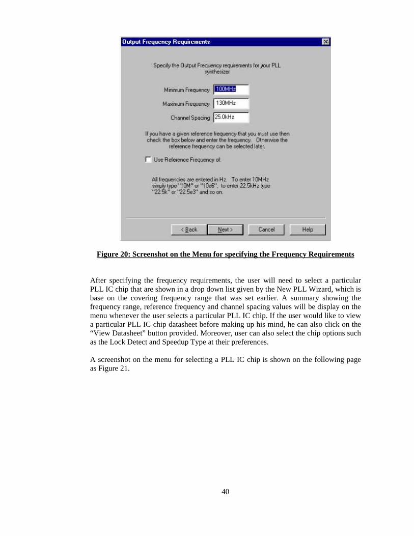
40
Figure 20: Screenshot on the Menu for specifying the Frequency Requirements After specifying the frequency requirements, the user will need to select a particular PLL IC chip that are shown in a drop down list given by the New PLL Wizard, which is base on the covering frequency range that was set earlier. A summary showing the frequency range, reference frequency and channel spacing values will be display on the menu whenever the user selects a particular PLL IC chip. If the user would like to view a particular PLL IC chip datasheet before making up his mind, he can also click on the “View Datasheet” button provided. Moreover, user can also select the chip options such as the Lock Detect and Speedup Type at their preferences. A screenshot on the menu for selecting a PLL IC chip is shown on the following page as Figure 21.

41
Figure 21: Screenshot on the Menu for selecting a PLL IC chip Following next, the user will need to select the loop filter configuration for their PLL design. There will be a few variety of loop filter configuration to choose from and all the configurations shown in the menu actually matches the Phase Detector and Speedup Mode that were selected earlier. A screenshot on the menu for selecting the loop filter configuration is shown on the following page as Figure 22.

42
Figure 22: Screenshot on the Menu for selecting the Loop Filter Configurations After selecting the desired loop filter configuration for the PLL design, the user will need to select a VCO for their PLL design. They can either choose from the existing library files or they can customize their own VCO. However, by selecting a custom VCO requires entering the tuning sensitivity, Kv. A screenshot on the menu for selecting a VCO is shown on the following page as Figure 23.

43
Figure 23: Screenshot on the Menu for selecting a VCO
Lastly, the user will move on to select or input their desired reference frequency. Similarly to selecting a VCO, user can either choose their desired external reference oscillator from the existing library files or they can customize their own crystal oscillator by specifying the desired reference frequency. A screenshot on the menu for selecting the reference frequency is shown on the following page as Figure 24.

44
Figure 24: Screenshot on the Menu for selecting the Reference Frequency Then, the tutorial will goes on informing the user how to navigate the tutorial navigation buttons, what are the navigation tabs available and also the main screen description. The tutorial will also include some information on how the user can customize his/her PLL and how to use some of the useful features (e.g. Marker/Enable feature) that are already built within the ADIsimPLL simulation software. At the same time, it also covers some information on topics such as Transient Simulation, Phase Noise Calculation, Changing Loop Filters, Lock Detect Circuits and so on and so for. No matter if the user is in the tutorial session or normal session, there are always 2 panels displayed on the screen. One of them is the Data Panel, which shows the data settings for the Reference Oscillator, the VCO, the PLL Synthesizer IC chip, the Loop Filter and etc. The Data Panel is displayed on the left hand side of the screen and it is the panel that can controls most of the data entry to ADIsimPLL. The Data Panel provides the main path where the user can alter the loop bandwidth, change the charge pump current, and add in some leakage current and so on. Some of the data settings that are shown in this Data Panel were the one that are defined at the beginning stage by the user as explained earlier. The others are those data settings that can either be change or not change by the user throughout the phase of designing a PLL. Notice that those data settings that can be change or set by user are highlighted within a green coloured box. As for those data settings that cannot be set or change by the user, it will not have any green coloured box around it. User can always change
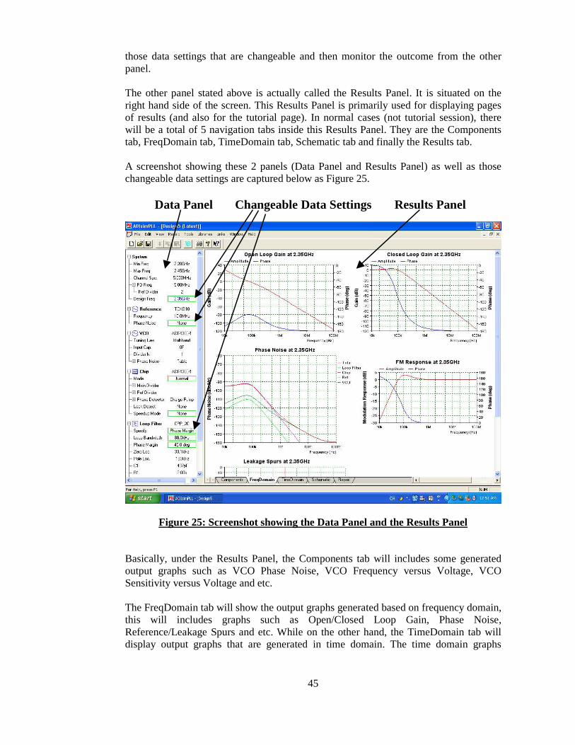
45
those data settings that are changeable and then monitor the outcome from the other panel. The other panel stated above is actually called the Results Panel. It is situated on the right hand side of the screen. This Results Panel is primarily used for displaying pages of results (and also for the tutorial page). In normal cases (not tutorial session), there will be a total of 5 navigation tabs inside this Results Panel. They are the Components tab, FreqDomain tab, TimeDomain tab, Schematic tab and finally the Results tab. A screenshot showing these 2 panels (Data Panel and Results Panel) as well as those changeable data settings are captured below as Figure 25.
Figure 25: Screenshot showing the Data Panel and the Results Panel Basically, under the Results Panel, the Components tab will includes some generated output graphs such as VCO Phase Noise, VCO Frequency versus Voltage, VCO Sensitivity versus Voltage and etc. The FreqDomain tab will show the output graphs generated based on frequency domain, this will includes graphs such as Open/Closed Loop Gain, Phase Noise, Reference/Leakage Spurs and etc. While on the other hand, the TimeDomain tab will display output graphs that are generated in time domain. The time domain graphs
Data Panel Results Panel Changeable Data Settings

46
generated out includes graphs such as Frequency, Absolute Frequency Error, Output Phase Error and etc. As the name specifies, the Schematic tab will provide the user with the schematic diagram on the selected PLL synthesizer IC chip and its connections. Finally, the Report tab will list a summary of all the output results such as the Phase Noise at particular frequencies offset define by the user, the Lock Time with respect to frequency and phase and etc in figures format or in a table form. An example showing all these 5 navigation tabs inside the Results Panel can be found as Appendix F in this dissertation. From here, based on all these output graphs and results generated by ADIsimPLL, user is able to know the performance and capability of their PLL design. If user is not satisfy with the outcome or would like to improve their PLL design in some ways, they can always change some of the data settings on the Data Panel so as to enhance their PLL design accordingly. In normal PLL design case, just right after the user select he/her desired loop filter configurations, ADIsimPLL will provide a default value of the loop bandwidth and phase margin to get the simulation started. However, user can still set his/her own desired loop filter bandwidth and phase margin at anytime later to optimize the PLL design. In any PLL design, the loop filter bandwidth is an important parameter that requires much attention to it. User can vary the loop filter bandwidth to compensate for different part of the PLL design such as the Lock Time or the Phase Noise performance. As mentioned before, when using ADIsimPLL, at anytime of the PLL design phase, user can still change the loop filter bandwidth to his/her preference if they would like to improve on any part of their PLL design’s performance. Each new design will always commences with the New PLL Wizard and go through the starting phase of defining the frequency requirements, selecting the VCO and etc. At any stage of the design process, the user can save their PLL design file as a .pll file. By saving the design file as a .pll file will saves the workspace, everything in the Data Panel and the locations of the graphs on the results pages. However, currently for ADIsimPLL version 3.0, it does not save the marker locations, custom graph scales or saved traces in the graphs. To get a hardcopy of the results pages and the report from ADIsimPLL, user can simply click on the page they wish to print (ensuring the mouse pointer has the focus) and then click on the print icon on the toolbar. To copy a graph or schematics onto a word processor such as Microsoft Word, user can simply right click on the graph or schematics and select copy, followed by selecting paste onto the word processor.
4.3 Usage of ADIsimPLL
When using the ADIsimPLL, there are a few features that are quite interesting and useful. One of them is called the Marker/Enable feature. The user can enable a marker on any of the generated output graph. In order to do this, user can just simply right click on the particular graph chosen and on the menu that appears select “” . The marker will then appears as a brown dashed vertical line on the graph, with a black triangle at the bottom. It will initially appear in the middle of the graph. Basically, the black triangle at

47
the bottom acts as a “handle” that allows the user to drag with the mouse to move the marker to any desired location on the graph. An example showing how the marker can be used to determine the lock time to 100 Hz is shown on the following page as Figure 26.
0 0.5 1.0 1.5 2.0 2.5Time (ms)
100m
1
10
100
1k
10k
100k
1M
10M
100M
Ab
s F
req
uen
cy E
rro
r (H
z)
1.502ms 81.080 Hz
|Freq Error|
Figure 26: Example showing the Usage of the Marker Feature From the above graph, by using the Marker/Enable feature, we can see that the lock time to 100 Hz is around 1.5ms. Whenever the graph is not selected, the marker handle will disappear but the marker and its display will still remains. To move the marker again, user just need to click on the graph and the marker handle will reappear. Another interesting feature that ADIsimPLL provides is the Save Trace feature. Before the user alter any changeable data settings such as the loop bandwidth to see if the changes made will optimise the PLL performance or not, he/she can simply right click on the Phase Noise graph on the FreqDomain tab and click on the Save Trace menu item. This will saves the trace of the current phase noise performance for comparison with the new results after changing the loop bandwidth. An example showing how the save trace feature works is shown below as Figure 27.
10 100 1k 10k 100k 1MFrequency (Hz)
-160
-150
-140
-130
-120
-110
-100
-90
-80
-70
-60
Ph
ase
No
ise
(dB
c/H
z)
Phase Noise at 114MHz
Figure 27: Example showing the Usage of the Save Trace Feature
Marker
Red Trace
Pink Trace

48
The pink trace that is shown on the above graph indicates the previous phase noise performance results while the red trace on the above graph indicates the new phase noise performance results. With this feature, user can easily compare and know what is the outcome of his/her changes made and there is no need for the user to spend unnecessary time to set back to the previous settings to compare the results with the new one. This Save Trace feature can be use for all types of generated output graphs from the ADIsimPLL simulation software. Apart from using the ADIsimPLL for simulation purposes, it can also be use as a testing software by an engineer or anyone who wanted to know the performance of a particular PLL synthesizer IC chip that they are interested in before they decided to buy the chip or the evaluation board from Analog Devices. After trying out and if the output performance really suits what they want for the output results, they can then purchase these PLL synthesizer IC chip or the evaluation board from Analog Devices, knowing roughly what will be the output results of it. This will resulted in an increase in efficiency when using this particular PLL synthesizer IC chip or the evaluation board and at the same time helps companies or individuals to save money in buying unsuitable or incompatible PLL synthesizer IC chip or evaluation board.

49
5. RESULTS
The Work Breakdown Structure (WBS) provided in the Appendix B shows that the project has been underway since the first week of March 2006. In fact, some of the research was started from early January 2006 onwards. From the first week of March 2006 onwards till now, almost all the tasks were accomplished according to the timeline schedule in the WBS except for the measuring process on the evaluation board (due to the unforeseen difficulties and constraints faced). All the milestones reflected in the methodology flowchart of Figure 1 in Chapter 1 were also almost accomplished although there are some delays in finishing some of tasks within the milestones. At the first milestone, the planning stage phase was completed after defining the way of working, the tasks required to be completed and the overall general planning required in running this project. The second milestone, the research and reviewing phase was completed as discussed in Chapter 2, Background of this dissertation whereby all researched information and work reviewed are illustrated. The actual due date for this milestone is being planned to be completed is by 31 August 2006. This is to allow continuous gathering of more details information and data at a slower rate until the time to start writing the dissertation. The third milestone, sourcing of available resources is described in Appendix D, Resource requirements and planning of this dissertation. Whenever there is any insufficient information faced during the next milestone, measuring and stimulating, more work had been carried out in these milestones concurrently with other processes. The fourth milestone that was completed is basically the measuring and stimulating milestone. After the purchased evaluation board had reached Singapore on the 1st of June 2006, the starting of this milestone was then carried out. The measuring experiment had been performed on the ADF4360-1 evaluation board as described in Chapter 3 and the stimulating of ADF4360-1 synthesizer IC chip using the ADIsimPLL simulation software was also covered in Chapter 4. The fifth milestone on evaluating and comparing of the results will be discussed in this chapter and the sixth milestone on recommendation and conclusion will be covered in the last chapter, Discussion and Conclusion of this dissertation. Last but not least, the final milestone, which is the documentation and reporting, is just simply the documentation of all the work done and things/lessons learnt into this dissertation. Throughout the whole project phase, in order to update the project supervisor on the current progress of the project at all times, a weekly progress report had been created. This weekly progress report will be updated accordingly and send to the project supervisor in weekly basis. A sample of the weekly progress report that was submitted for Week 637 is captured as Appendix I in this dissertation. As detailed in Chapter 3, all the test points of the ADF4360-1 evaluation board had been measured in order to get the actual performance results of this evaluation board. In Chapter 5.1, it will present the output results from all these measurements made. Following that, in Chapter 5.2, the output results on the simulation done with

50
ADF4360-1 synthesizer IC chip by using the ADIsimPLL simulation software will then be discussed.
5.1 Results on Hardware Evaluation
As mentioned in Chapter 3, the first measurements are being carried out by powering up the evaluation board and connecting the probe from Channel 1 of the Tektronix TDS3014B high speed oscilloscope to the respective test points with the ground pin of the probe connected to the ground point of the evaluation board, Test Point, T4. The first measurements output results on the waveforms for the Test Point, T1 and T2 are shown below as Figure 28 and 29 respectively.
Figure 28: Test Point T1 Output Waveform using Tektronix TDS3014B
Figure 29: Test Point T2 Output Waveform using Tektronix TDS3014B

51
At the same time, a table had been drawn up to record the voltage readings (in V or mV), the time/period readings (in ns) as well as the frequency readings (in MHz) for each individual test points on the evaluation board. This table can be found under Appendix J of this dissertation. From all the output waveforms displayed from the Tektronix TDS3014B high speed oscilloscope, it can be seen that only Test Point T1 and T2 shows a definite shape waveforms (e.g. some sort of a square or sine wave), the other 9 test points only shows some sort of a DC straight line output waveforms. Test Point T1 is actually connected to the TCX010 external reference oscillator of 10 MHz and Test Point T2 is actually connected to the input of the REFIN pin (which is Pin 16 of the ADF4360-1 frequency synthesizer IC chip). From the readings in the table under Appendix J, it can be seen that only Test Point T1 and T2 have period and frequency recorded, the other 9 test points have no period or frequency shown on the measurement scale displayed on the Tektronix TDS3014B. Since the measurement results from the first measurements seem to be a bit strange and incorrect as most of the other test points have some sort of a DC straight line output waveforms, therefore, in order to verify and make sure what had been measured so far are actually correct, a second round of measurements on all the test points had been carried out using the LeCroy Wave Surfer 424 high speed oscilloscope. The output waveforms for the Test Point, T1 and T2 for the second measurements are shown below as Figure 30 and 31 respectively.
Figure 30: Test Point T1 Output Waveform using LeCroy Wave Surfer 424

52
Figure 31: Test Point T2 Output Waveform using LeCroy Wave Surfer 424 Similarly to the first measurements, a table had also been drawn up to record the voltage readings (in V or mV), the time/period readings (in ns) as well as the frequency readings (in MHz) for each individual test points on the evaluation board. This table can be found under Appendix K of this dissertation. From all the output waveforms displayed from the LeCroy Wave Surfer 424 high speed oscilloscope, it can be seen that again only Test Point T1 and T2 shows a definite shape waveforms (e.g. some sort of a square or sine wave), the other 9 test points only shows some sort of a DC straight line output waveforms. From the readings in the table under Appendix K, it can be seen that again only Test Point T1 and T2 have both period and frequency recorded, the other 9 test points have unstable or no period or frequency shown on the measurement scale displayed on the LeCroy Wave Surfer 424. One of the example output waveform from the other 9 test points such as Test Point T3 is display as Figure 32 shown on the following page. It has a voltage peak-to-peak value of 14 mV, ground to positive voltage peak value of 6 mV, ground to negative voltage peak value of -8 mV. The unstable values for Test Point T3 period and frequency are reflected as 6.865 ns and 145.7 MHz respectively. As indicated by LeCroy Wave Surfer 424, those values displayed with this icon “” seen below means that the values are unstable and may not be correct. Thus, these types of values are reflected as a “-” in the table under Appendix K.

53
Figure 32: Test Point T3 Output Waveform using LeCroy Wave Surfer 424 With this second round of measurements, it proved that the measured values in the first round of measurements should be correct, however the values and the output waveforms for the other 9 test points still seem to be incorrect. After checking these measurement results with the Applications Engineer from Analog Devices, it was realized that there is a need to program the registers for the R Counter, Control Latch and N Counter first using the ADF4360 evaluation board programmable software before starting to measure all the test points and the parameters on the board that are required for future 3G applications. As discussed in Chapter 3.4, a lot of unforeseen difficulties and limitations were encountered when using this ADF4360 evaluation board programmable software and conducting the measuring experiment, hence, eventually, the process of measuring the ADF4360-1 evaluation board performance are being supplemented by using the simulation software from Analog Devices, called the ADIsimPLL instead. Unfortunately, when using the ADIsimPLL, some of the requirements or parameters that are needed for future 3G applications still needs to be measured physically using the ADF4360-1 evaluation board. This means in another word, some of these future 3G requirements values cannot be found by using the ADIsimPLL. The only way to retrieve their values is by the means of measuring the ADF4360-1 evaluation board again. These requirements or parameters that need to be measured physically are shown the following page.
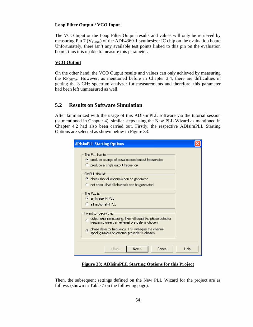
54
Loop Filter Output / VCO Input The VCO Input or the Loop Filter Output results and values will only be retrieved by measuring Pin 7 (VTUNE) of the ADF4360-1 synthesizer IC chip on the evaluation board. Unfortunately, there isn’t any available test points linked to this pin on the evaluation board, thus it is unable to measure this parameter. VCO Output On the other hand, the VCO Output results and values can only achieved by measuring the RFOUTA. However, as mentioned before in Chapter 3.4, there are difficulties in getting the 3 GHz spectrum analyzer for measurements and therefore, this parameter had been left unmeasured as well.
5.2 Results on Software Simulation
After familiarized with the usage of this ADIsimPLL software via the tutorial session (as mentioned in Chapter 4), similar steps using the New PLL Wizard as mentioned in Chapter 4.2 had also been carried out. Firstly, the respective ADIsimPLL Starting Options are selected as shown below in Figure 33.
Figure 33: ADIsimPLL Starting Options for this Proj ect Then, the subsequent settings defined on the New PLL Wizard for the project are as follows (shown in Table 7 on the following page).

55
Minimum Frequency: 2.20 GHz Maximum Frequency: 2.45 GHz Phase Detector Frequency / Channel Spacing: 5.00 MHz Select PLL Chip: ADF4360-1 Integrated-N PLL Chip Lock Detect: None Speedup Type: None VCO Divider: div = 1 Loop Filter Configuration: Charge Pump Passive 2 Capacitors type (which is same as the one shown on Figure 22) PLL Reference Selection: From Library, Model: “TCX010”, Frequency: 10.0 MHz Loop Bandwidth: 10 KHz (which is the default setting for the actual ADF4360-1 evaluation board loop bandwidth value) Phase Margin: 45 degree
Table 7: Phase Noise with Loop Bandwidth of 10 KHz
Since ADF4360-1 synthesizer IC chip has an in-built VCO, thus there is no need to select any desired VCO from the ADIsimPLL software. Next, the values for the other requirements or parameters (apart from the VCO input and output) that are needed for future 3G applications are being retrieved by tackling one by one using the ADIsimPLL software as shown in the following sections. Channel Spacing Generally, for an Integer-N PLL, the Phase Frequency Detector (PFD) frequency is equal to the step size, which is also equal to the channel spacing as well as the Phase Detector Frequency (PDF). Using ADIsimPLL simulation software with ADF4360-1 synthesizer chip chosen as the base, the channel spacing is actually user specified as set in Table 7. However, in order to select an appropriate value for the channel spacing, there is one important criterion, which is related to the reference frequency that needs to be taken care of. A reference frequency is a stable frequency that the PLL uses to generate an output frequency. Standard values of an external reference oscillator are those that are already available in the market. A custom value of an external reference oscillator is the one that mathematically will work, but it may be a custom order from an external reference/crystal manufacturer. Now, the criteria is that the reference frequency must be an integer multiple of the channel spacing. Since the external reference oscillator chosen in the ADF4360-1 evaluation board is the TCXO10 external reference oscillator with a reference frequency of 10 MHz, thus eventually the channel spacing was chosen to be 5 MHz, which is the same as the current 3G requirements. Lock Time (Frequency & Phase) Both the requirements “acquisition time after switching to a new frequency (to get within one cycle slip of new frequency)” and “time required to change channels” are all referring to the same parameter known as the “lock time” with respect to Analog Devices terminology. The values of this lock time can be found by looking at the

56
Absolute Frequency Error graph generated by the ADIsimPLL software or by looking at the Frequency Locking Time stated in the Report tab under ADIsimPLL software. The Absolute Frequency Error graph generated for this project using the ADF4360-1 synthesizer IC chip is shown below as Figure 34.
0 10 20 30 40 50 60 70 80Time (us)
100m 1 10
100 1k10k
100k 1M10M
100M 1G
Abs
Fre
quen
cy E
rro
r (H
z)
|Freq Error|
Figure 34: Absolute Frequency Error Graph
For the requirement on the “settling time (for phase error to decrease from near 360 degrees to near zero)”, it is also referring to the “lock time” with respect to Analog Devices terminology. Just that now, the values of this lock time can be found by looking at the Output Phase Error graph generated by the ADIsimPLL software (as shown below as Figure 35) instead or by looking at the Phase Locking (VCO Output Phase) Time stated in the Report tab under ADIsimPLL software.
0 10 20 30 40 50 60 70 80Time (us)
-50 -40 -30 -20 -10
010 20 30 40 50
Pha
se E
rro
r (de
g)
Output Phase Error
Figure 35: Output Phase Error Graph

57
Logically, an increase in the loop bandwidth will speeds up the lock time but at the same time decrease the phase noise performance. Hence, to find out a suitable value for the loop bandwidth in order to have the best trade off between the lock time and phase noise, a few rounds of trial and error experiments had been conducted using the ADIsimPLL simulation software. First of all, the following parameters are being set on the New PLL Wizard and the Data Panel inside the ADIsimPLL software.
i. PLL output/operating frequency = 2.35 GHz ii. Loop bandwidth = 10 KHz iii. Phase Margin = 45 degrees iv. Channel Spacing = 5 MHz v. TCX010 Crystal Oscillator / Reference frequency = 10 MHz
Since the actual default value of the loop bandwidth for ADF4360-1 evaluation board is define as 10 KHz, thus in our first trial and error experiment, the loop bandwidth is set at 10 KHz. This loop bandwidth value of 10 KHz is considered as the initial starting point or can be treated as the lowest value for the loop bandwidth to have a stable loop. The Phase Noise Table generated by the ADIsimPLL software is as shown below in Table 8. Phase Noise Table Freq Total VCO Ref Chip Filter 100 -94.05 -99.34 -- -95.57 -135.8 1.00k -88.40 -89.38 -- -95.37 -115.9 10.0k -84.04 -84.68 -- -93.25 -101.9 100k -110.7 -110.8 -- -127.9 -135.9 1.00M -132.0 -132.0 -- -167.9 -175.8 10.0M -150.0 -150.0 -- -207.9 -215.8 100M -159.6 -159.6 -- -247.9 -255.8 1.00G -160.0 -160.0 -- -287.7 -294.4 2.35G -160.0 -160.0 -- -298.2 -299.6
Table 8: Phase Noise with Loop Bandwidth of 10 KHz
The Frequency Locking Time and the Phase Locking (VCO Output Phase) Time stated in the Report tab of ADIsimPLL software are as shown below in Table 9. Frequency Locking Time to lock to 1.00 Hz is 397 µs Time to lock to 5.00MHz is 8.99 µs Phase Locking (VCO Output Phase) Time to lock to 1.00 deg is 286 µs Time to lock to 45.0 deg is 189 µs
Table 9: Frequency and Phase Locking Time with Loop Bandwidth of 10 KHz

58
Following next, the loop bandwidth is then set to a very high value until just before the loop becomes unstable (in another word. This value is found to be 790 KHz, which can be considered as the final ending point or can be treated as the highest value for the loop bandwidth to have a stable loop. The following parameters are set under the Data Panel inside the ADIsimPLL software.
i. PLL output/operating frequency = 2.35 GHz ii. Loop bandwidth = 790 KHz iii. Phase Margin = 45 degrees iv. Channel Spacing = 5 MHz v. TCX010 Crystal Oscillator / Reference frequency = 10 MHz
The Phase Noise Table generated by the ADIsimPLL software is as shown below in Table 10. Phase Noise Table Freq Total VCO Ref Chip Filter 100 -95.57 -175.2 -- -95.57 -192.8 1.00k -95.57 -165.2 -- -95.57 -172.8 10.0k -95.56 -155.3 -- -95.56 -152.8 100k -95.25 -139.3 -- -95.25 -132.8 1.00M -95.09 -128.9 -- -95.10 -122.5 10.0M -132.0 -149.9 -- -132.0 -158.9 100M -159.4 -159.6 -- -172.0 -198.9 1.00G -160.0 -160.0 -- -212.0 -238.9 2.35G -160.0 -160.0 -- -226.9 -253.8
Table 10: Phase Noise with Loop Bandwidth of 790 KHz The Frequency Locking Time and the Phase Locking (VCO Output Phase) Time stated in the Report tab of ADIsimPLL software are as shown below in Table 11. Frequency Locking Time to lock to 1.00 Hz is 5.83 µs Time to lock to 5.00MHz is 1.62 µs Phase Locking (VCO Output Phase) Time to lock to 1.00 deg is 3.01 µs Time to lock to 45.0 deg is 1.83 µs Table 11: Frequency and Phase Locking Time with Loop Bandwidth of 790 KHz
From here, the loop bandwidth is then slowly reduced and this resulted in slowing down the transient as well. Finally, in order to strike a balance between both the lock time and the phase noise, which are consider as the important requirements for future 3G applications, the loop bandwidth is being reduce to a most suitable value of 80 KHz.

59
The following parameters are set under the Data Panel inside the ADIsimPLL software.
i. PLL output/operating frequency = 2.35 GHz ii. Loop bandwidth = 80 KHz iii. Phase Margin = 45 degrees iv. Channel Spacing = 5 MHz v. TCX010 Crystal Oscillator / Reference frequency = 10 MHz
The Phase Noise Table generated by the ADIsimPLL software is as shown below in Table 12. Phase Noise Table Freq Total VCO Ref Chip Filter 100 -95.57 -135.5 -- -95.57 -162.9 1.00k -95.56 -125.5 -- -95.57 -142.9 10.0k -95.21 -115.5 -- -95.26 -123.0 100k -94.69 -107.9 -- -94.98 -112.4 1.00M -128.8 -131.9 -- -131.8 -148.8 10.0M -150.0 -150.0 -- -171.8 -188.8 100M -159.6 -159.6 -- -211.8 -228.8 1.00G -160.0 -160.0 -- -251.8 -268.8 2.35G -160.0 -160.0 -- -266.6 -283.5
Table 12: Phase Noise with Loop Bandwidth of 80 KHz
The Frequency Locking Time and the Phase Locking (VCO Output Phase) Time stated in the Report tab of ADIsimPLL software are as shown below in Table 13. Frequency Locking Time to lock to 1.00 Hz is 50.2 µs Time to lock to 5.00MHz is 2.00 µs Phase Locking (VCO Output Phase) Time to lock to 1.00 deg is 28.9 µs Time to lock to 45.0 deg is 18.3 µs
Table 13: Frequency and Phase Locking Time with Loop Bandwidth of 80 KHz
By comparing these new settings with the previous 2 settings, the lock time to lock to 5 MHz (which is from 1 channel to another) as stated here will be about 4.5 times faster than the lock time to lock to 5 MHz with loop bandwidth of 10 KHz and about 0.8 times slower than the lock time to lock to 5 MHz with loop bandwidth of 790 KHz. Moreover the phase noise with loop bandwidth of 80 KHz is still maintaining in quite a good performance as compare to the one with loop bandwidth of 790 KHz. The phase noise graph for both the loop bandwidth of 10 KHz and 80 KHz are reflected as Figure 36. The pink trace represents the total phase noise graph with loop bandwidth set at 10 KHz, while the red trace represents the total phase noise graph with loop bandwidth set at 80 KHz.

60
10k 100k 1M 10M 100MFrequency (Hz)
-160
-150
-140
-130
-120
-110
-100
-90
-80
-70
-60
Pha
se
No
ise
(dB
c/H
z)
Phase Noise at 2.35GHz
TotalLoop FilterChipRefVCO
Figure 36: Total Phase Noise Graph at 2.35 GHz with Loop Bandwidth of 80 KHz
The Frequency graph for the loop bandwidth of 80 KHz is reflected as Figure 37 as shown below. From this Frequency graph, notice that the output VCO frequency first raises from 2.28 GHz to about 2.456 GHz within the first 1 microsecond and after that it fluctuates and final get stabled at 2.45 GHz (which is the desired output VCO frequency) after 10 microseconds.
0 10 20 30 40 50 60 70 80Time (us)
2.282.302.32
2.342.36
2.382.40
2.422.44
2.46
Fre
que
ncy
(GH
z)
Frequency
Figure 37: Frequency Graph with Loop Bandwidth of 80 KHz
Red Trace
Pink Trace

61
In conclusion, with the loop bandwidth set at 80 KHz, it improved the lock time to lock to 5.00 MHz from original 8.99 µs (based on loop bandwidth of 10 KHz) to 2.00 µs and improve the phase time to lock to 45.0 degrees from original 189 µs (based on loop bandwidth of 10 KHz) to 18.3 µs. At the same, notice that with loop bandwidth set at 80 KHz, the phase noise performance at Frequency 100 KHz and 1 MHz is not degraded so much as compare to the setting with loop bandwidth of 790 KHz. Phase Noise For phase noise, it is always the lower the phase noise (which means the larger negative value), the better the phase noise performance will be. (E.g. -160dBc/Hz is better than -150dBc/Hz). Inside the ADIsimPLL simulation software, the VCO's in the library files can have tabulated phase noise data (and this is how recommended measured VCO's are modelled). The VCO built inside the ADF4360-1 evaluation board has a phase noise Floor of -160dBc/Hz from the table of VCO library files. Which means, at 2.35 GHz or 2.45 GHz, the phase noise is at -160dBc/Hz. As mentioned earlier, any changes to the loop bandwidth will have direct impact on the phase noise. From the generated phase noise graph as shown below in Figure 38, the phase noise has a significant hump around the loop bandwidth and the initial reaction may be that the phase margin is poor. In fact, the actual main reason for the hump to be present around the loop bandwidth is due to the excellent phase noise performance of the ADF4360-1 synthesizer chip, which causes the noise inside the loop bandwidth to be low.
10k 100k 1M 10M 100MFrequency (Hz)
-160
-150
-140
-130
-120
-110
-100
-90
-80
-70
-60
Pha
se N
oise
(dB
c/H
z)
Phase Noise at 2.35GHz
TotalLoop FilterChipRefVCO
Figure 38: Phase Noise Graph at 2.35 GHz with Loop Bandwidth of 80 KHz
Bright Green Trace
Pale Green Trace

62
As we currently have an ideal external reference oscillator (TCX010), the only noise contributions come from the VCO, Chip and the Loop Filter. The Chip clearly dominates at low frequencies, the VCO at high frequencies, but around the 'hump' there are similar contributions from all three components. From the phase noise graph shown in Figure 38, you can see that the loop filter contribution for the lower current implementation [Charge Pump (CP) Current: 313 µA] contributes substantially greater noise when compares to the loop filter contribution for the higher current implementation [Charge Pump (CP) Current: 2.50 mA]. As displayed in the above phase noise graph in Figure 38, the pale green trace indicates the phase noise performance of the loop filter with Charge Pump (CP) Current of 2.50 mA while the bright green trace indicates the phase noise performance of the loop filter with Charge Pump (CP) Current of 313 µA. Higher charge pump currents generally reduce phase noise; however they result in larger loop filter capacitors. Smaller currents reduce the size of the filter capacitors, but increase the resistor value(s) resulting in an increase in phase noise. Changing the charge pump current does not change the lock time if the loop bandwidth is kept constant. This can be easily verified by changing the charge pump current under the Data Panel and look at the lock time under the Report tab of the Results Panel in the ADIsimPLL simulation software. As mentioned earlier in Chapter 3, the type of loop filter configuration chosen for this project is the Charge Pump Passive 2 Capacitors type. Any changes made on this loop filter configuration, will resulted in a change in the lock time and phase noise performance even if the loop bandwidth is kept constant at 80 KHz.

63
6. DISCUSSION AND CONCLUSIONS
6.1 Results Discussion
After using the ADIsimPLL simulation software to design for a suitable frequency synthesizer (based on ADF4360-1 synthesizer chip) for future 3G applications and optimised the lock time by increasing the loop bandwidth with the best trade off between the lock time and phase noise, the values of most of the requirements or parameters mentioned in the previous chapter are found. These parameters values from the frequency synthesizer design created by ADIsimPLL are then compared with other manufacturer’s frequency synthesizer design (based on datasheets only) as well as future 3G predicted requirements (based on whatever information found in the Internet and books). For easy visualization and comparison, 2 comparison tables on these requirements between the synthesizer design created by ADIsimPLL and the other manufacturer’s frequency synthesizer design had been drawn up as shown in Table 14 and 15 on the following pages. From Table 14, notice that when compared the time required to change channels or the lock time between the ADF4360-1 and ADF4360-0 frequency synthesizer IC chips, with the same preset settings, the ADF4360-1 synthesizer chip seems to have a slightly better and a faster lock time than ADF4360-0 synthesizer chip. From Table 14, ADF4360-1 synthesizer chip have a lock time to lock to 5 MHz at 2 µs whereas the ADF4360-0 synthesizer chip have a lock time to lock to 5 MHz at 2.4 µs. When comparing this lock time for ADF4360-1 synthesizer chip with the typical lock time for both the LMX2310U and LMX2347 frequency synthesizer IC chips, ADF4360-1 synthesizer chip is obviously better as it is designed and optimised by the user using ADIsimPLL simulation software. When comparing the phase noise at 2.5 KHz within the final frequency under Table 14, ADF4360-0 synthesizer chip have a slightly better performance than the ADF4360-1 synthesizer chip but still, LMX2347 have the best phase noise performance of -83 dBc/Hz at 2.5 KHz within the final frequency. However, both the LMX2310U and LMX2347 synthesizer chips from National Semiconductors have a fixed operating frequency range at only 2.5 GHz which made them less flexible as compared to the ADF4360-1 and ADF4360-0 synthesizer chips which has the operating frequency range from 2.05 GHz to 2.45 GHz and 2.4 GHz to 2.725 GHz respectively.
From Table 15, when comparing the phase noise performance at 1 MHz within the final frequency, TRF3761 synthesizer chip from Texas Instrument have a better phase noise performance of -138 dBc/Hz than the ADF4360-1 synthesizer chip. At the same time, a comparison table on these requirements between the synthesizer design created by ADIsimPLL and the future 3G predicted synthesizer design based on the information found in the Internet and books had been drawn up as Table 16 shown on the following pages as well.

64
Manufacturer Analog Devices National Semiconductor Model No ADF4360-1 ADF4360-0 LMX2310U LMX2347 Operating Frequency Range
2.05 GHz to 2.45 GHz 2.4 GHz to 2.725 GHz 2.5 GHz 2.5 GHz
Time required to change channels
Time to lock to 1.00 Hz is 47.2 µs Time to lock to 5 MHz is 2 µs
Time to lock to 1.00 Hz is 49.8 µs Time to lock to 5 MHz is 2.4 µs
500 µs (Typical) 450 µs (Typical)
VCO Inputs and Outputs
Need to measure VTUNE (Pin 7). Need to measure VTUNE (Pin 7). No evaluation board. No evaluation board.
Filter Outputs Need to measure VTUNE (Pin 7). Need to measure VTUNE (Pin 7). No evaluation board. No evaluation board.
Acquisition time after switching to a new frequency (to get within one cycle slip of new frequency)
Loop bandwidth = 80 KHz Phase Margin = 45 degrees
Operating Frequency = 2.45 GHz Channel Spacing = 5 MHz
Reference Oscillator Frequency = 10 MHz Frequency Locking
Time to lock to 1.00 Hz is 47.2 µs Time to lock to 5 MHz is 2 µs
(from ADIsimPLL)
Loop bandwidth = 80 KHz Phase Margin = 45 degrees
Operating Frequency = 2.45 GHz Channel Spacing = 5 MHz
Reference Oscillator Frequency = 10 MHz Frequency Locking
Time to lock to 1.00 Hz is 49.8 µs Time to lock to 5 MHz is 2.4 µs
(from ADIsimPLL)
Not available from datasheet
Not available from datasheet
Settling time (for phase error to decrease from near 360 degrees to near zero)
Loop bandwidth = 80 KHz Phase Margin = 45 degrees
Operating Frequency = 2.45 GHz Channel Spacing = 5 MHz
Reference Oscillator Frequency = 10 MHz Phase Locking
Time to lock to 45.0 deg is 17 µs Time to lock to 1.00 deg is 27.2 µs
(from ADIsimPLL)
Loop bandwidth = 80 KHz Phase Margin = 45 degrees
Operating Frequency = 2.45 GHz Channel Spacing = 5 MHz
Reference Oscillator Frequency = 10 MHz Phase Locking
Time to lock to 45.0 deg is 16.4 µs Time to lock to 1.00 deg is 26.2 µs
(from ADIsimPLL)
Not available from datasheet
Not available from datasheet
Channel Spacing Max. 8 MHz (user-specified) Max. 8 MHz (user-specified) Max. 10 MHz Max. 10 MHz
Phase Noise at a specified offset from the output
Operating Frequency = 2.45 GHz Channel Spacing = 200 KHz
Reference Oscillator Frequency = 10 MHz Loop Bandwidth = 12 KHz Phase Margin = 45 degrees
Phase Noise = -79.74 dBc/Hz at 2.5 KHz within the final frequency
(from ADIsimPLL)
Operating Frequency = 2.45 GHz Channel Spacing = 200 KHz
Reference Oscillator Frequency = 10 MHz Loop Bandwidth = 12 KHz
Phase Noise = -79.81 dBc/Hz at 2.5 KHz within the final frequency
(from ADIsimPLL)
Operating Frequency = 2.45 GHz
Channel Spacing = 200 KHz
Reference Oscillator Frequency = 10 MHz Loop Bandwidth = 12
KHz Phase Noise = -78 dBc/Hz at 2.5 KHz within the final
frequency (from Datasheet)
Operating Frequency = 2.45 GHz
Channel Spacing = 200 KHz
Reference Oscillator Frequency = 10 MHz Loop Bandwidth = 12
KHz Phase Noise = -83 dBc/Hz at 2.5 KHz within the final
frequency (from Datasheet)
Table 14: Comparison Table 1 on Requirements between the Synthesizer Design created by ADIsimPLL and the other manufacturer's Frequency Synthesizer Design

65
Table 15: Comparison Table 2 on Requirements between the Synthesizer Design created by ADIsimPLL and the other
manufacturer's Frequency Synthesizer Design
Manufacturer Analog Devices Texas Instrument Singapore Technologies Model No ADF4360-1 ADF4360-0 TRF3761 STW81100 Operating Frequency Range
2.05 GHz to 2.45 GHz 2.4 GHz to 2.725 GHz 375 MHz to 2.4 GHz 825 MHz to 4.4 GHz
Time required to change channels
Time to lock to 1.00 Hz is 47.2 µs Time to lock to 5 MHz is 2 µs
Time to lock to 1.00 Hz is 49.8 µs Time to lock to 5 MHz is 2.4 µs
300 µs (Typical) 150 µs (Typical)
VCO Inputs and Outputs
Need to measure VTUNE (Pin 7). Need to measure VTUNE (Pin 7). No evaluation board. No evaluation board.
Filter Outputs Need to measure VTUNE (Pin 7). Need to measure VTUNE (Pin 7). No evaluation board. No evaluation board.
Acquisition time after switching to a new frequency (to get within one cycle slip of new frequency)
Loop bandwidth = 80 KHz Phase Margin = 45 degrees
Operating Frequency = 2.45 GHz Channel Spacing = 5 MHz
Reference Oscillator Frequency = 10 MHz Frequency Locking
Time to lock to 1.00 Hz is 47.2 µs Time to lock to 5 MHz is 2 µs
(from ADIsimPLL)
Loop bandwidth = 80 KHz Phase Margin = 45 degrees
Operating Frequency = 2.45 GHz Channel Spacing = 5 MHz
Reference Oscillator Frequency = 10 MHz Frequency Locking
Time to lock to 1.00 Hz is 49.8 µs Time to lock to 5 MHz is 2.4 µs
(from ADIsimPLL)
Not available from datasheet
Not available from datasheet
Settling time (for phase error to decrease from near 360 degrees to near zero)
Loop bandwidth = 80 KHz Phase Margin = 45 degrees
Operating Frequency = 2.45 GHz Channel Spacing = 5 MHz
Reference Oscillator Frequency = 10 MHz Phase Locking
Time to lock to 45.0 deg is 17 µs Time to lock to 1.00 deg is 27.2 µs
(from ADIsimPLL)
Loop bandwidth = 80 KHz Phase Margin = 45 degrees
Operating Frequency = 2.45 GHz Channel Spacing = 5 MHz
Reference Oscillator Frequency = 10 MHz Phase Locking
Time to lock to 45.0 deg is 16.4 µs Time to lock to 1.00 deg is 26.2 µs
(from ADIsimPLL)
Not available from datasheet
Not available from datasheet
Channel Spacing Max. 8 MHz (user-specified) Max. 8 MHz (user-specified) Max. 30 MHz Max. 10 MHz
Phase Noise at a specified offset from the output
Operating Frequency = 2289 MHz Channel Spacing = 200 KHz
Reference Oscillator Frequency = 10 MHz Loop Bandwidth = 15 KHz Phase Margin = 45 degrees
Phase Noise = -131.8 dBc/Hz at 1 MHz within the final frequency
(from ADIsimPLL)
Operating Frequency = 2400 MHz Channel Spacing = 200 KHz
Reference Oscillator Frequency = 10 MHz Loop Bandwidth = 15 KHz Phase Margin = 45 degrees
Phase Noise = -132.8 dBc/Hz at 1 MHz within the final frequency
(from ADIsimPLL)
Operating Frequency = 2289 MHz
Channel Spacing = 200 KHz
Reference Oscillator Frequency = Unknown Loop Bandwidth = 15
KHz Phase Noise = -138
dBc/Hz at 1 MHz within the final frequency (from
Datasheet)
Operating Frequency = 2200MHz
Channel Spacing = Unknown
Reference Clock Signal = 19.2MHz
Loop Bandwidth = Unknown
Phase Noise = -61 dBc/Hz at 1 KHz within the final
frequency (from Datasheet)

65
PLL Design Specifications required
for 3G Applications
PLL Design Specifications concluded from the information found in Internet for current 3G
Specification
My own PLL Design Specifications based on
ADF4360-1 chip
Frequency Range 1.5 GHz to 3 GHz 2.25 GHz to 2.45 GHz
Step Size 5 MHz Step Size = Channel Spacing =
PDF frequency = user-defined (5 MHz)
Channel Spacing 1.25 MHz to 5 MHz 5 MHz
Phase Noise at a specific offset from the output
For an output frequency of 1.9 GHz, the TRF3761 delivers -138
dBc/Hz phase noise when measured at a 600 kHz offset, and noise floor of -160 dBc/Hz when
measured at a 10 MHz offset.
For an output frequency of 2.35 GHz, this own created PLL
design delivers -121.5 dBc/Hz phase noise when measured at a
600 kHz offset, and noise floor of -160 dBc/Hz when measured at a
10 MHz offset.
Acquisition time after switching to a new frequency (to get within one cycle slip of new frequency)
80 ms
Loop bandwidth = 80 KHz Phase Margin = 45 degrees
Operating Frequency = 2.35 GHz Channel Spacing = 5 MHz
Reference Oscillator Frequency = 10 MHz
Frequency Locking Time to lock to 1.00 Hz is 47.2 µs
Time to lock to 5 MHz is 2 µs (from ADIsimPLL)
Settling time (for phase error to decrease from near 360 degrees to near zero)
Typically 200 µs
Loop bandwidth = 80 KHz Phase Margin = 45 degrees
Operating Frequency = 2.35 GHz Channel Spacing = 5 MHz
Reference Oscillator Frequency = 10 MHz
Phase Locking Time to lock to 45.0 deg is 17 µs Time to lock to 1.00 deg is 27.2
µs (from ADIsimPLL)
Switching Time / Time required to change channels
Not Available
Loop bandwidth = 80 KHz Phase Margin = 45 degrees
Operating Frequency = 2.35 GHz Channel Spacing = 5 MHz
Reference Oscillator Frequency = 10 MHz
Frequency Locking Time to lock to 1.00 Hz is 47.2 µs
Time to lock to 5 MHz is 2 µs (from ADIsimPLL)
Spurious signal level Not Available No spurious signal level Power consumption/dissipation
Max. Tx Power 30dBm (1W) Min. Tx Power -50dBm
Not Available
Table 16: Comparison Table on Requirements between Synthesizer Design created
by ADIsimPLL and the Future 3G predicted Synthesizer Design
66

66
Since it was impossible to gather all the data on the other manufacturers’ synthesizer IC chips that are required to compare with the ADF4360-1 frequency synthesizer design, therefore it was unable to fully select and justified which is the best frequency synthesizer design for future 3G applications. Hence, in conclusion, after optimizing the performance of the ADF4360-1 synthesizer IC chip using the ADIsimPLL software, ADF4360-1 seems to have a good performance that is suitable for future 3G applications. When comes to lock time to lock to 5 MHz (which is switching from 1 channel to another with channel spacing of 5 MHz), it has the best performance so far although the phase noise performance is not the best out of all the other frequency synthesizer IC chips.
6.2 Conclusion
This dissertation has summarized the work involved in fulfilling the objectives of the project. Although, quite a lot of work had been completed in this project, however there are still some more researches and experiments required before we can actually define exactly what will be the future 3G requirements and parameters. Throughout the whole project phase, besides learning how the PLL frequency synthesizer actually works, what are the different types of frequency synthesizer techniques available and the important key parameters inside a frequency synthesizer, I also get to learnt what is the history of the mobile systems generations, how 3G systems comes about, how WCDMA functions and etc. Apart from all these, I also get the chance to learn how to use some of the up to date measuring equipment such as the Tektronix TDS3014B and the LeCroy Wave Surfer 424 high speed oscilloscopes which I had not yet seen before. Not to forget, I had also learnt how to use the dynamic ADIsimPLL simulation software from Analog Devices. In the near future, the future 3G systems or the 4G systems will be developed. One of the main objectives of developing the future 3G systems or the 4G systems is to overcome the shortcomings and limitations of the current 3G systems. Future 3G systems or 4G systems will focus more on the following key points.
i) Offer higher bandwidth up to 100 Mbps ii) Allows global roaming iii) Enhanced network architecture, having entirely a packet switched network iv) Accommodate a collection of wireless networks v) Provides asymmetrical services
This will also mean that the future 3G or 4G systems will need to have the requirements cater for all these above mentioned key points. As mentioned before in Chapter 2, the current 3G systems offer maximum bandwidth up to 2 Mbps, however in practical the bandwidth available to the users can be less than 2 Mbps. Even though the bandwidth offered by 3G systems is higher than 2G systems, it is still actually insufficient to support all the different types of multimedia communications. That is the reason why currently Singapore is looking at enhancing the bandwidth or the data rate by using the High Speed Downlink Packet Access (HSDPA) for downlink transmission. Performance-wise, High Speed Packet Access (HSPA)
67

67
offers data transfer rates comparable with Digital Subscriber Line (DSL) but with full mobility, service continuity and roaming. Moreover, HSPA has the unique capability to support virtually any known mobile or Internet service.
The HSPA phase provides typical average speeds of around 1 Mbps downlink and 0.5 to 1 Mbps uplink, the peak speeds being multiple times higher, up to 14.4 Mbps. The requirements have already been agreed in 3GPP and targets have been set to increase data rates to reach up to 100 Mbps, as well as to achieve further increased spectral efficiency and reduced latency. With the HSPA technology, it will enhance the bandwidth up to 100 Mbps and at the same time leads future 3G systems or 4G systems networks into more of a packet switched networks. As mentioned in the earlier chapters, 3G technologies were originally proposed to provide global roaming. Global roaming here implies that whenever any subscriber roams across the globe, he/she would always remain connected. However, in the end, a set of five standards under the IMT-2000 was adopted for 3G networks. The reason for having multiple standards is to encourage competition and also to cater for the migration of the Second Generation (2G) networks for different 2G standards that are already defined in different countries. This means that the current 3G implementations had failed to achieve the requirement of global roaming. Hence, in future 3G systems or 4G systems, the target of providing global roaming is required to be achieved. Currently, 3G networks consist of both the circuit switched and packet switched domains. However, for future 3G or 4G networks, it will be expected to be base entirely on packet switched network using Internet Protocol (IP). Basically, IP is a packet exchange protocol for Internet works, and allows the connection between any two hosts that are connected to the Internet no matter whether they are on the same or sub networks. There are a number of problems associated with the use of IP in 3G networks. IP does not support real time quality of service and requires other protocols to do this. IP will require real time support in order for it to offer a wide range of services, such as data and multimedia. Internet Protocol version 4 (IPv4) is the main version used on the Internet today. 3GPP has stated that Internet Protocol version 6 (IPv6) will be the alternative protocol for future releases of the 3G standards or for the future 3G systems. For 3GPP, its current developments about IP issue could be divided in two aspects. The first one is the provision of Internet connectivity to the mobile station, and the other one is using IP technology in the interior of the mobile network (Wikipedia, 4G, July 2006). Thus, by using IP within the packet switched networks will allows the accommodation of different wireless network such as the Internet, personnel area networks and etc. From the viewpoint of providing asymmetric services (such as Internet access) in the future 3G systems, it is expected that the Time Division Duplex (TDD) mode of operation would be more suitable when compared to the Frequency Division Duplex (FDD) mode. FDD mode is used for the paired spectrum while TDD is used for unpaired spectrum. In the FDD mode of operation, two separate 5 MHz carrier frequencies with equal bandwidths are used in the uplink and downlink direction. In the TDD mode of operation, only one 5 MHz carrier is time-shared between the uplink and downlink. The main benefit of TDD mode is that the bandwidths in forward and backward direction can be altered. Which means it is possible to have a downlink
68
68
bandwidth much more than the uplink bandwidth. This can be very helpful especially in Internet applications (e.g. downloads from Internet) whereby a small request is followed by a large amount of information. The unpaired nature of TDD makes it use the spectrum more efficiently. Furthermore, as the spectrum becomes scarce in the near future, getting an unpaired spectrum will be much easier as compared to attaining a paired spectrum. With all these advantages mentioned above, it would not be surprise to see TDD becoming more popular than FDD in the near future. TDD is also presumed to be use in hot spots (e.g. bus interchange) so as to provide high data rate connectivity. In conclusion, in the future 3G systems, mobile networks would be able to offer richer services than today's wireless communication network can do. Users could easily create their own personal area networks and with the integration of the 3G systems, Wireless Local Area Network (WLAN), and Public Switched Telephone Network (PSTN) network, it will be able to offer the possibility of achieving anywhere, anytime Internet access (Uskela, 2003).
6.3 Suggestions for Future Work
If more time are given and if all the required non-human resources such as the 3 GHz spectrum analyzer and other measuring equipment are available for the project, the hardware evaluation portion to get the measured parameters necessary for future 3G applications would have been able to be accomplish. Thus, one of suggestions for future work is to focus more on the hardware evaluation and get the measured parameters values from the ADF4360-1 evaluation board. Then, compared these measured values to the one that had been simulated using the ADIsimPLL software to see if they are matched and indeed suitable for future 3G applications or not. On-going research and experiment with respect to future or post 3G requirements needs to be carry out again in order to be always aligned with what had been done for the project since any new changes or updates on the future 3G requirements announced by 3GPP or other 3G systems bodies (such as ITU and etc) will affect the outcome of this project as well.
69

69
7. REFERENCES
1. 3G Phones, 2006, 3G Standards, viewed 4 October 2006, <http://www.three-g.net/3g_standards.html>.
2. 3GPP, 21 April 2006, Shaping the future of mobile communication standards,
viewed 14 April 2006, <http://www.3gpp.org/>. 3. Analog Devices, Inc., 1995-2006, PLL Synthesizers/VCOs, viewed 2 May 2006,
<http://www.analog.com/en/subCat/0,2879,770%255F850%255F0%255F%255F0%255F,00.html>.
4. Analog Dialogue, Curtin Mike and O'Brien Paul, Volume 33, Number 7,
July/August, 1999, Phase Locked Loops for High-Frequency Receivers and Transmitters-3, viewed on 5 July 2006, <http://www.analog.com/library/analogDialogue/archives/33-07/phase3/>.
5. Egan William F., 1990, Frequency Synthesizer by Phase Lock, Robert E. Krieger
Publishing, Malabar. 6. GSA - The Global mobile Suppliers Association, September 2006, GSA News,
viewed 11 September 2006, <www.gsacom.com>. 7. GSM World, 2006, GSM Platform, viewed 5 July 2006,
<http://www.gsmworld.com/technology/3g/evolution.shtml>. 8. Holma Harri and Toskala Antti, 2000, WCDMA For UMTS Radio Access for Third
Generation Mobile Communications, John Wiley & Sons, Ltd. 9. IS224 Project 1, Spring 1999, The Dynamics of Standards Creation in the Global
Wireless Telecommunications Markets, viewed on 9 April 2006, <http://www.sims.berkeley.edu:8000/courses/is224/s99/GroupD/project1/paper1.html>.
10. Kasera Sumit and Narang Nishit, 2004, 3G Networks Architecture, Protocols and
Procedures, Tata McGraw-Hill Publishing Company Limited. 11. National Semiconductor Corporation, 02-May-2006, LMX2310U - 2.5 GHz
PLLatinum Ultra Low Power Frequency Synthesizer for RF Personal Communications, viewed 2 May 2006, <http://www.national.com/search/search.cgi/main?keywords=LMX2310U%20&%20LMX2347%20Evaluation%20Board>.
12. Radio Electronics, 2006, ElectroStatic Discharge (ESD) Tutorial, viewed on 2 June
2006, <http://www.radio-electronics.com/info/circuits/esd/electrostatic_discharge.php>.
13. STMicroelectronics, Multi-band RF Frequency Synthesizer with Integrated VCO,
viewed 2 May 2006, <http://www.st.com/stonline/books/ascii/docs/11297.htm>.
70

70
14. Texas Instruments, TRF3761 Low Noise Integer N PLL Frequency Synthesizer With Integrated VCO, viewed 2 May 2006, <http://focus.ti.com/docs/prod/folders/print/trf3761.html?DCMP=hpa_rf_general&HQS=ProductBulletin+OT+trf3761>.
15. UMTS Forum, 22 June 2000, WARC-92 frequencies of IMT-2000 resolution,
Björnsjö Krister, viewed 9 April 2006, <http://www.3gpp.org/ftp/TSG_SA/TSG_SA/TSGS_08/Docs/PDF/SP-000257.pdf>.
16. UMTS Forum, 11 June 2003, Spectrum for future UMTS / IMT-2000 Requirements,
viewed 25 May 2006, <http://www.3g.co.uk/PR/June2003/5476.htm>. 17. UMTS Forum, 2006, UMTS Forum News, viewed 9 April 2006, <http://www.umts-
forum.org/servlet/dycon/ztumts/umts/Live/en/umts/Home>. 18. Uskela Sami, Key Concepts for Evolution toward Beyond 3G Networks, IEEE
Wireless Communications, Feb. 2003. 19. Wikipedia, July 2006, 4G, viewed 4 October 2006,
<http://en.wikipedia.org/wiki/4G>. 20. Wikipedia, 27 October 2006, History of mobile phones, viewed 4 October 2006,
<http://en.wikipedia.org/wiki/History_of_mobile_phones#Early_years>.
71
71
8. BIBLIOGRAPHY
1. 3G, 2 October 2003, 3G Mobile Phone Testing, viewed 14 April 2006,
<http://www.3g.co.uk/PR/Oct2003/5907.htm>. 2. 3G Phones, 2006, 3G Standards, viewed 4 October 2006, <http://www.three-
g.net/3g_standards.html>. 3. 3GPP, 21 April 2006, Shaping the future of mobile communication standards,
viewed 14 April 2006, <http://www.3gpp.org/>. 4. Analog Devices, Inc., 1995-2006, PLL Synthesizers/VCOs, viewed 2 May 2006,
<http://www.analog.com/en/subCat/0,2879,770%255F850%255F0%255F%255F0%255F,00.html>.
5. Analog Dialogue, Curtin Mike and O'Brien Paul, Volume 33, Number 7,
July/August, 1999, Phase Locked Loops for High-Frequency Receivers and Transmitters-3, viewed on 5 July 2006, <http://www.analog.com/library/analogDialogue/archives/33-07/phase3/>.
6. Chevillat Pierre R. and Schott Wolfgang, 27 February 2003, Broadband radio LANs
and the evolution of wireless beyond 3G, IBM Journal of Research and Development, viewed 09 April 2006, <http://www.research.ibm.com/journal/rd/472/chevillat.html>.
7. Cui Hongyan, Cai Yunlong, Wang Ying, Zhang Ping, Design and Implementation
of all IP Architecture for Beyond 3G System, IEEE Communications Society, 2004. 8. Egan William F., 1990, Frequency Synthesizer by Phase Lock, Robert E. Krieger
Publishing, Malabar. 9. GSA - The Global mobile Suppliers Association, September 2006, GSA News,
viewed 11 September 2006, <www.gsacom.com>. 10. GSM World, 2006, GSM Platform, viewed 5 July 2006,
<http://www.gsmworld.com/technology/3g/evolution.shtml>. 11. Holma Harri and Toskala Antti, 2000, WCDMA For UMTS Radio Access for Third
Generation Mobile Communications, John Wiley & Sons, Ltd. 12. IS224 Project 1, Spring 1999, The Dynamics of Standards Creation in the Global
Wireless Telecommunications Markets, viewed on 9 April 2006, <http://www.sims.berkeley.edu:8000/courses/is224/s99/GroupD/project1/paper1.html>.
13. Kasera Sumit and Narang Nishit, 2004, 3G Networks Architecture, Protocols and
Procedures, Tata McGraw-Hill Publishing Company Limited.
72

72
14. Naraine Patrick, 1 February 2005, Direct modulation radio hardware architectures for 3G communications systems, RF Design, viewed 14 April 2006, <http://rfdesign.com/mag/radio_direct_modulation_radio/>.
15. National Semiconductor Corporation, 02-May-2006, LMX2310U - 2.5 GHz
PLLatinum Ultra Low Power Frequency Synthesizer for RF Personal Communications, viewed 2 May 2006, <http://www.national.com/search/search.cgi/main?keywords=LMX2310U%20&%20LMX2347%20Evaluation%20Board>.
16. PR Newswire, 20 October 2005, Texas Instruments Introduces New Radio
Frequency Synthesizer for Wireless Infrastructure Applications, viewed 14 April 2006, <http://www.sys-con.com/read/143670.htm>.
17. Radio Electronics, 2006, ElectroStatic Discharge (ESD) Tutorial, viewed on 2 June
2006, <http://www.radio-electronics.com/info/circuits/esd/electrostatic_discharge.php>.
18. RTT Hot Topic, October 2005, The role of Hadamard-Rademacher-Walsh
transforms in present and future radio systems, IBM Journal of Research and Development, viewed 9 April 2006, <http://www.rttonline.com/HotTopics/HT_Oct05.htm>.
19. STMicroelectronics, Multi-band RF Frequency Synthesizer with Integrated VCO,
viewed 2 May 2006, <http://www.st.com/stonline/books/ascii/docs/11297.htm>. 20. Texas Instruments, TRF3761 Low Noise Integer N PLL Frequency Synthesizer With
Integrated VCO, viewed 2 May 2006, <http://focus.ti.com/docs/prod/folders/print/trf3761.html?DCMP=hpa_rf_general&HQS=ProductBulletin+OT+trf3761>.
21. UMTS Forum, 22 June 2000, WARC-92 frequencies of IMT-2000 resolution, Krister
Björnsjö, viewed 9 April 2006, <http://www.3gpp.org/ftp/TSG_SA/TSG_SA/TSGS_08/Docs/PDF/SP-000257.pdf>.
22. UMTS Forum, 11 June 2003, Spectrum for future UMTS / IMT-2000 Requirements,
viewed 25 May 2006, <http://www.3g.co.uk/PR/June2003/5476.htm>. 23. UMTS Forum, 2006, UMTS Forum News, viewed 9 April 2006, <http://www.umts-
forum.org/servlet/dycon/ztumts/umts/Live/en/umts/Home>. 24. Uskela Sami, Key Concepts for Evolution toward Beyond 3G Networks, IEEE
Wireless Communications, Feb. 2003. 25. Wikipedia, July 2006, 4G, viewed 4 October 2006,
<http://en.wikipedia.org/wiki/4G>. 26. Wikipedia, 27 October 2006, History of mobile phones, viewed 4 October 2006,
<http://en.wikipedia.org/wiki/History_of_mobile_phones#Early_years>.
73

73
9. APPENDICES
9.1 Appendix A – Project Specifications
The Project Specifications that have been agreed between the project supervisor and the student are stated as shown below.
ENG 4111/4112 Research Project
PROJECT SPECIFICATION
FOR: Woo Mun Kit TOPIC: Frequency synthesizer requirements for future cellular radio systems SUPERVISOR: Associate Professor Jim Ball
SPONSORSHIP: Faculty of Engineering & Surveying, USQ
ENROLMENT: ENG 4111 – S1, X, 2006; ENG 4112 – S2, X, 2006
PROJECT AIM: This project aims to evaluate the synthesizer requirements of future radio systems, which will probably involve a mixture of technology evaluation and simulation.
PROGRAMME: Issue B, 10th September 2006
1. Become familiar with 3G and post 3G radio preliminary standards. (Timeline: Immediate start – Completion date 31 August 06)
2. Survey available frequency synthesizer technologies and design techniques.
(Timeline: Immediate start – Completion date 31 August 06) 3. Decide on a frequency synthesizer evaluation board and ask USQ to purchase. Price
limit is about $AU200. Synthesizer should be close in performance to 3G requirements for channel frequency and spacing etc., but an exact match is not likely or necessary. (Timeline: Completion date 16 April 06)
4. Measure the parameters and performance of the frequency synthesizer evaluation board. (Timeline: Completion date 01 September 06)
5. Simulate the dynamic behaviour of this synthesizer chosen by the means of using a
simulation software and get the parameters that are required for 3G applications from it. In particular, try to stimulate and get the time required to change channels. (Timeline: Completion date 15 September 06)
74

74
6. Evaluate this synthesizer design against future requirements for 3G and post 3G so as to see if the same general design will be adequate or not. Also evaluate other designs, as an exercise on paper with no measurements. (Timeline: Completion date 15 September 06)
7. Comparison of synthesizer designs, and formulation of recommendations as to which designs are likely to be suitable for 3G and post 3G radio. (Timeline: Completion date 15 September 06)
8. Write first draft of project report/dissertation and provide to supervisor for comment
and advice. (Timeline: Start 15 September 06 – Completion date 09 October 06)
9. Complete final draft of project report/dissertation for submission.
(Timeline: Start 20 October 06 – Completion date 02 November 06) 10. Return frequency synthesizer evaluation board to USQ.
(Timeline: By 30 November 06)
75

75
9.2 Appendix B – Timelines Planning and Work Breakdown Structure (WBS)
At the start of the project, one of the important tasks is to plan the timeline for the project as it will helps both the supervisor and the student himself/herself to oversee the progress of the whole project. Most importantly it gives a guideline of the approximate time frame allowed and effort required for each milestone and important deadlines for the project. The timelines schedule is also being reflected in Appendix B, which includes both the resource tracking plan and the Work Breakdown Structure (WBS) for Wk 635, which is being extended for both ENG4111 and ENG4112 modules. It illustrates the planned timelines for major milestones or activities that need to be completed in terms of number of weeks. Generally, from the WBS, more time is allocated for the research that needs to be carried out on 3G and future 3G radio preliminary standards as well as the survey that needs to be performed on the current available frequency synthesizer technologies and design techniques. This is because in order to use the measured and stimulated performance of the evaluation board synthesizer design against future requirements for 3G and future 3G, it requires some understandings on the current 3G mobile radio standards, plans for future 3G and some basic behaviours of the Phase Locked Loop synthesizers. Moreover, it is also a good practice to start the survey on the available frequency synthesizer evaluation boards in the early stage as there may be substantial delays in delivery, especially for small orders. Due to time constraints, some of the tasks are being planned in the way to run concurrently at the same time. However, there are some tasks that can only proceed after another task had been complete. Refer to the WBS of Appendix B for such tasks that are cascaded (one followed after by another). These tasks may require more attention as one task delayed may directly affect the rest of the tasks behind. Notice also from the WBS, there are coloured boxes indicating the status of each and every task. This helps to track if the tasks are being completed on time or if there is a need for more time to complete the task. The planned status will be in pink colour, while the on-going status and completed status are being reflected in blue and green colour respectively. Time deviation against the planned task completion duration is also captured in this WBS in red colour. Thus, if the student or the project supervisor wants to track the reasons why there is a delay or why the time needed to complete the task is longer than planned, they can simply refer to these red boxes. The red boxes reflected in the WBS are due to unforeseen events that required more time to investigate and to complete the task.
76

76
Appendix B – Timelines Planning and Work Breakdown Structure (WBS) Resource Tracking Planned Resources March, 2006 April, 2006 May, 2006 June, 2006 July, 2006 August, 2006
Summary Total 609 610 611 612 613 614 615 616 617 618 619 620 621 622 623 624 625 626 627 628 629 630 631 632 633 634 635
Remus Woo 15 0.5 0.5 0.8 0.8 0.4 0.4 0.8 0.8 0.8 0.4 0.4 0.4 0.8 0.8 0.8 0.8 0.1 0.1 0.1 0.3 0.8 0.8 0.8 0.4 0.8 0.8 0.8 WBS
March, 2006 April, 2006 May, 2006 June, 2006 July, 2006 August, 2006 Actions To Do 609 610 611 612 613 614 615 616 617 618 619 620 621 622 623 624 625 626 627 628 629 630 631 632 633 634 635
Prepare Project Specification Search for Frequency Synthesizer Specs/details to decide on a frequency synthesizer evaluation board to purchase Prepare Project Appreciation Prepare Progress Assessment Measure performance of evaluation board
Evaluate synthesizer design of evaluation board against future requirements for 3G & Post 3G Research on 3G & post 3G radio preliminary standards Survey available Frequency Synthesizer technologies & design techniques Compare synthesizer design & recommend which designs for Post 3G Radio System First Draft of Project Dissertation for supervisor to comment
Final Draft of Project Dissertation for submission Return frequency synthesizer evaluation board to USQ Planned Ongoing Completed Deviation
77

77
9.3 Appendix C – Risk Assessment and Management
In nature, there are 2 types of risks. One of them is the risk that will affect directly on the progress of the project or what we normally called as Project Risks. The other type of risk is basically referring to the risk that will cause a potential threat to personal or public safety. The details on project risks as well as safety issues will be covered in the following sections under Appendix C of this dissertation.
9.3.1 Project Risks
At the start of the project, a Risk Assessment and Management Plan (RAMP) had been created for project risk tracking purposes. Any predicted upcoming project risks that might happen in the near future or any project risks that are encountered during the project running phase will be captured in this Risk Assessment and Management Plan for tracking. For every risk item identified, the Effect or Impact it has on the project will be stated. Original risk factor will also be calculated based on the Probability of Occurrence and the Severity of the risk. To minimize or eliminate the risk, mitigation actions will also be planned and carried out. After carrying out the mitigation actions, the risk will be reviewed again and risk factor will be re-calculated again based on the current status. All the risk items identified will be track till closure with target and actual closure date defined.
9.3.2 Safety Issues
Although this project is mainly based on evaluating current 3G and future 3G requirements via investigation, measurement and simulation on a suitable frequency synthesizer evaluation board and it does not involves any heavy duty machineries, however there will still be chances where some safety issues can arise. Some of these safety issues that could arise in this project are being considered and listed down as follows. Electric shock When it comes to measuring on the performance of the frequency synthesizer evaluation board, there is need to power it up by either a power supply or by a computer. Measuring equipment such as frequency analyzer, oscilloscope and etc will also required electricity power in order to function. Hence if the connections and safety measures are not put into consideration, there might be a possibility of electric shock to the user or the student. Some safety measures to prevent such injury to occur would be:
• Operate all the power point connection and electrical equipment with dry hands instead of wet hands.
• Always ground yourself via a waist strip connected to the earth when handling electrical equipment and the frequency synthesizer evaluation board.
• Check that the power connections to all electrical equipment are being securely connected before powering up the equipment.
• Ensure no faulty power cords or cables are being used.
78
78
Appendix C – Risk Assessment and Management Foot Injury As this project will also involve using some bulky or heavy equipment such as spectrum analyzer or oscilloscope, thus there might be a risk that such heavy equipment will drop off from the table and landed onto the feet of the user or student. Therefore, it is always a good practice and a need to wear covered shoes (instead of non-covered shoes such as slippers) to protect your feet in the laboratory or in the testing environment. It is also advised to always put bulky or heavy equipment on a stable table before start using them. Burnt or Overheated Equipment If incorrect voltages or power are being supply to the electrical equipment or the frequency synthesizer evaluation board, it may burn and spoilt the electrical equipment or the evaluation board. Smokes that are harmful to human beings may be released out into the air, which directly pollutes the environment or the surroundings. For some worse cases, sparks or fires may also occur from this burnt or spoilt equipment that will eventually injured the user or the student himself/herself. If electrical equipment are being switched on for long hours even when it is not being used, it will also get overheated and eventually burnt out. Hence, some of the safety measures to prevent such issues to occur would be:
• Make sure correct voltages or polarity are being supply to the electrical equipment.
• Switch off the electrical equipment whenever they are not in use. • Check and make sure the power cords or cables and the power points are not
faulty and they are being certified with the Safety Mark from PSB Corporation. Apart from tracking the project risks, this Risk Assessment and Management Plan (RAMP) showing only 1 risk out of total 11 risks, as shown in the following page of this dissertation will also be used to track risks related to personal or public safety.
79

79
Appendix C – Risk Assessment and Management
Current Original
Risk Id Risk/ Issue Effect/Impact
Pro
bab
ility
of
Occ
ura
nce
(P
)
Sev
erit
y (S
)
Ris
k F
acto
r (P
*S)
Pro
bab
ility
of
Occ
ura
nce
(P
)
Sev
erit
y (S
)
Ris
k F
acto
r (P
*S)
Mitigating Action Owner Due Status Remarks Target
Closure Date
Actual Closure
Date
622.04 No proper anti electrostatic precaution is being put in place when handling the ADF4360-1 Evaluation Board
Resulted in having the ADF4360-1 Evaluation Board spoilt due to electrostatic discharge from the student.
Low B 2.0 Medium B 4.0 Need to look for suitable electrostatic discharge (ESD) wrist strap available in the lab, if not will need to purchase one from the electrical components store in Sim Lim Tower. Had look for suitable electrostatic discharge wrist strap available in the lab but unable to find and borrow one, hence, had purchase one from the electrical components store in Sim Lim Tower.
Remus 06/06/2006 Closed Had already ask around the lab in my working area but yet to confirm if there is any ESD wrist strap available or not. If not will need to look for a suitable one from the electrical components store in Sim Lim Tower. Having a proper ESD wrist strap to be connected to the person handling it will have 2 reasons. The first is safety, and the second is again to ensure that any static is removed in a controlled fashion.
06/06/2006 06/06/2006
Total Risk Exposure
34
Total Risk Exposure History
Mar Apr June July Aug Sep Oct Nov
Risk Exposure
0 2 2 18 12 5
Total Risk Exposure Trend
0
5
10
15
20
Jan Feb Mar Apr May June July Aug Sep Oct Nov
Ris
k E
xpo
sure
Risk Exposure
80

80
9.4 Appendix D – Resource Requirements and Planning
At the start of the project, resource requirements and planning are considered. Normally, we can classify resource into 2 categories, the human resource or the non-human resource such as equipment resource, books/references resource and etc. For human resource, it will be mainly contributed by the student himself/herself and a small portion of the resource support will comes from his/her supervisor. A resource tracking plan with respect to a Work Breakdown Structure had been created for this project so as to organize and track the usage of the human resource required as well as the tasks that need to be complete in this project. However, this resource tracking plan does not includes the small portion of the resource support from the project supervisor as it is mainly used to track the resource planning of the student. Appendix B shows the resource tracking plan and the Work Breakdown Structure for Wk 635 that had been created for this project. For non-human resource, it will be further divided into 2 parts, the equipment resource and the books/references resource. For equipment resource, it mainly covers the selected frequency synthesizer evaluation board, the register programming and simulation software that comes along with it as well as all the measuring and testing equipment that are essential for this project. The selected frequency synthesizer evaluation board (ADF4360-1EB1) is purchased at the cost of US$120 from Analog Devices. This evaluation board is sponsored by University of Southern Queensland, Faculty of Engineering and Surveying. The measuring and testing equipment such as the spectrum analysers and the high-speed oscilloscopes that are required to be used in this project are listed in the table below.
Equipment Name Model Specifications Probe Used Spectrum Analyser HP 8591E 100 KHz – 1.8GHz
Or 100 KHz – 3GHz 10 MHz bandwidth
High-Speed Oscilloscope
LeCroy Wave Surfer 424
200 MHz (2GS/s) 200 MHz bandwidth
High-Speed Oscilloscope
Tektronix TDS3014B
100 MHz (1.25GS/s) 10 MHz bandwidth
High-Speed Oscilloscope
Tektronix TDS3034B
300 MHz (2.5GS/s) 10 MHz bandwidth
High-Speed Oscilloscope
Tektronix VM5000
1 GHz (5GS/s) 10 MHz bandwidth
Table 17: Table on the Measuring Equipment used in the Project
For books/references resource, it is referring to library and reference books on PLL frequency synthesizer as well as on UMTS, 3G radio systems and etc. It also includes online Internet resources on frequency synthesizer, 3G and future 3G radio system
81

81
requirements and standards. Both the library references resources and Internet resources are accessible by the student.
82

82
9.5 Appendix E – Articles requesting for higher frequency band below 3 GHz
83

83
Appendix E – Articles requesting for higher frequency band below 3 GHz
84

84
9.6 Appendix F – Generated Output Results from ADIsimPLL v.3.0 Software
85
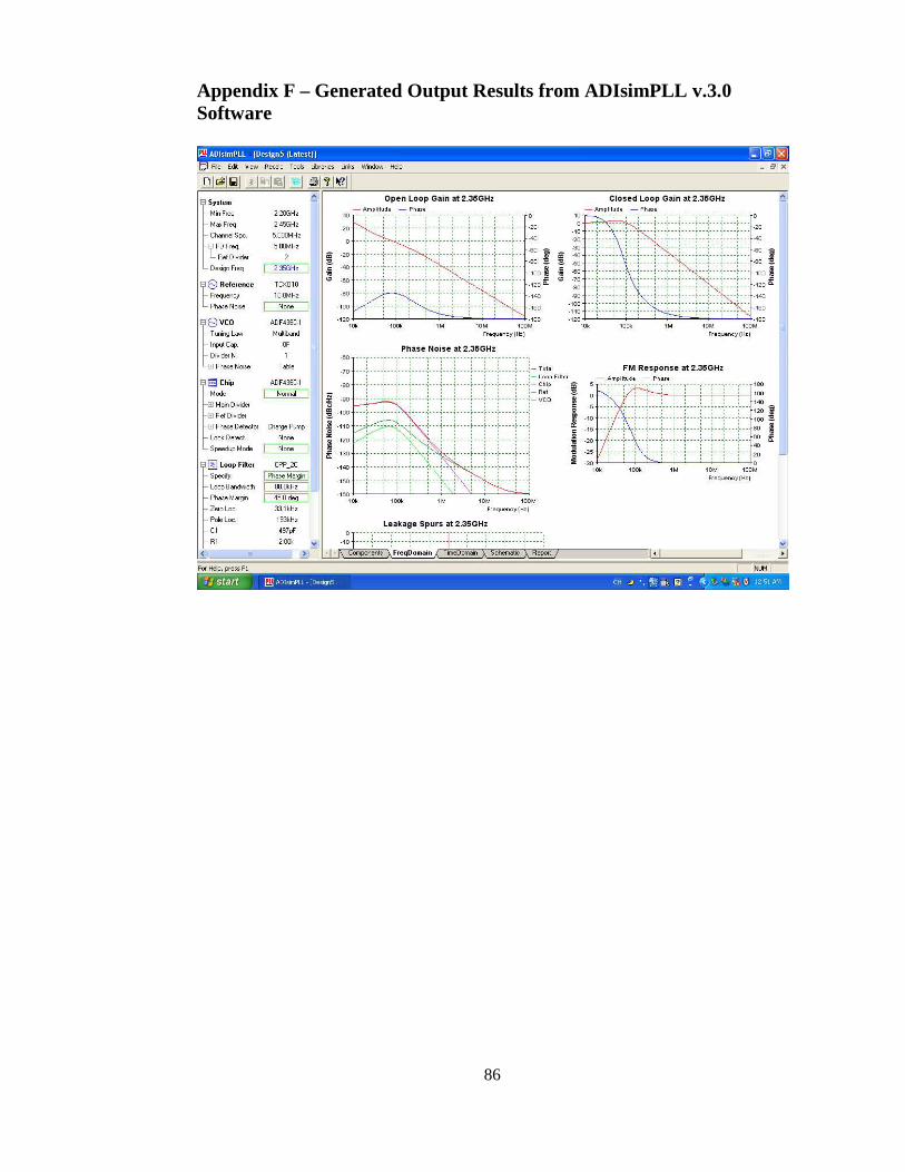
85
Appendix F – Generated Output Results from ADIsimPLL v.3.0 Software
86

86
Appendix F – Generated Output Results from ADIsimPLL v.3.0 Software
87

87
Appendix F – Generated Output Results from ADIsimPLL v.3.0 Software
88
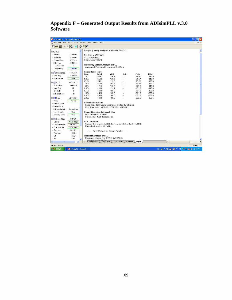
88
Appendix F – Generated Output Results from ADIsimPLL v.3.0 Software
89
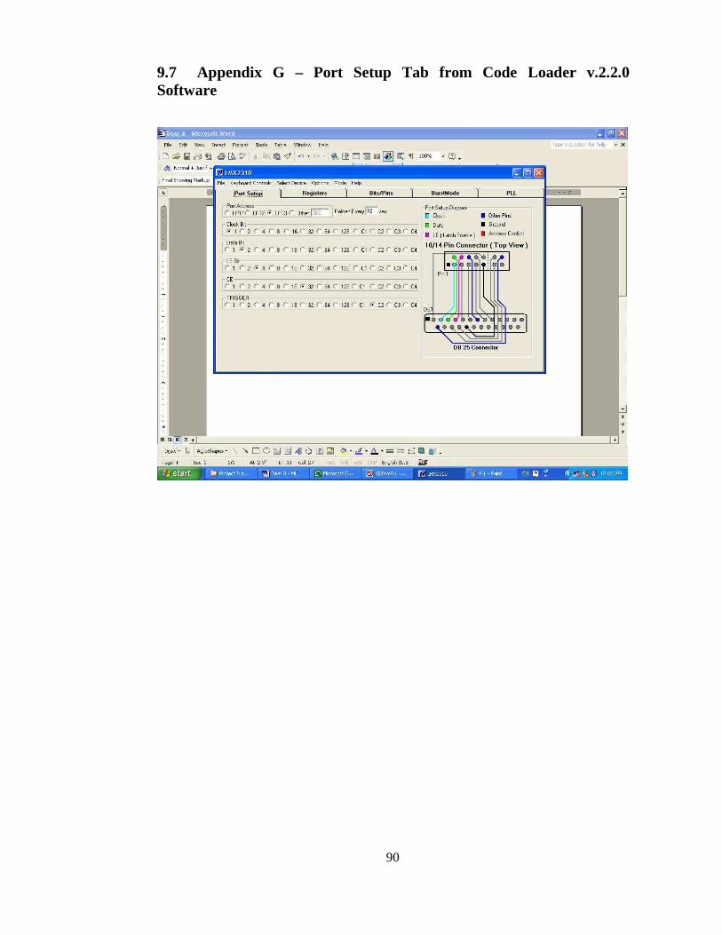
89
9.7 Appendix G – Port Setup Tab from Code Loader v.2.2.0 Software
90

90
9.8 Appendix H – PLL Tab from Code Loader v.2.2.0 Software
91

91
9.9 Appendix I – Weekly Progress Report for Wk 637
Sr. No. Highlights (Key Accomplishments/Updates) Traffic Light
1 Finish up and organise all the comparison values/data between the synthesizer design created using the ADIsimPLL simulation software (based on ADF4360-1 chip) as well as the other company's frequency synthesizer design and the post 3G predicted requirements.
2 Come up with the first Draft of Project Dissertation for supervisor to comment. Sr. No. Major Activities / Events Planned for the next 2-3 Weeks
1 Start looking into preparing of the presentation slides for ENG4903 Professional Practice 2 Residential School Trip on 2 Oct to 6 Oct 2006.
2 Try to meet up with A/Prof. Jim Ball on the first week of Residential School on 25 Sep to 29 Sep 2006 to align on the Project Specification, Project Dissertation and the Presentation Slides and preparation.
3 Try to go through the slides with A/Prof. Jim Ball after reviewed and reworked. If time permits, do a rehearsal as well. Sr. No. Lowlights (Not Accomplished) Traffic Light
Action
Sr. No. Risks / Issues to be Resolved (Key Issues) Traffic Light Supervisor Attention 1 Not enough time to meet all the requirements stated in the Project Specifications on time. Resulted in not able to finish
the project on time. • Plan to stay up late at night
over the weekends to finish it. • If really can't make it on time, request from extension from Supervisor, A/Prof. Jim Ball and A/Prof. Frank Young.
2 Not sure what to prepare inside the ENG4112 Presentation Slides. Resulted in not well prepared for the presentation during Residential School.
• Try to meet up with A/Prof. Jim Ball on the first week of Residential School on 25 Sep to 29 Sep 2006 to align on the Project Specification, Project Dissertation and the Presentation Slides and preparation. • Try to go through the slides with A/Prof. Jim Ball after reviewed and reworked. If time permits, do a rehearsal as well.
Legend for Traffic Light
Critical issue, need USQ Faculty of Engineering and Surveying attention
Major issue, need supervisor attention
Minor issue, can be managed by the student
92

92
9.10 Appendix J – 1st Measurements on all Test Points in ADF4360-1EB1
Test Point No.
Voltage Readings (V/mV)
Time/Period Readings (ns)
Frequency Readings (MHz)
T1 Vpp = 218 mV
Gnd to +Vp = 82 mV Gnd to -Vp = -136 mV
Period = 100.3 ns Frequency = 10 MHz
T2 Gnd to Vp = 1.46 V Period = 75 ns to
100 ns Frequency = 10 MHz
to 14 MHz
T3 Gnd to Vp = 1.5 V - -
T5 Gnd to Vp = 4.8 V - -
T6 Gnd to Vp = 2.88 V - -
T7 Gnd to Vp = 2.96 V - -
T8 Gnd to Vp = 2.96 V - -
T13 0 V - -
T14 0 V - -
T15 0 V - -
T16 Gnd to Vp = 2.96 V - -
Equipment Used: Tektronix TDS3014B High Speed Oscilloscope, 100MHz (1.25GS/s) Probe Used: 10 MHz Note: Test Point No. T4 is Ground.
93

93
9.11 Appendix K – 2nd Measurements on all Test Points in ADF4360-1EB1
Test Point No.
Voltage Readings (V/mV)
Time/Period Readings (ns)
Frequency Readings (MHz)
T1 Vpp = 267 mV
Gnd to +Vp = 89 mV Gnd to -Vp = -178 mV
Period = 99.896 ns Frequency = 10.0104
MHz
T2 Vpp = 233 mV
Gnd to +Vp = 53 mV Gnd to -Vp = -180 mV
Period = 100.088 ns Frequency = 9.9912
MHz
T3 Vpp = 14 mV
Gnd to +Vp = 6 mV Gnd to -Vp = -8 mV
- -
T5 Vpp = 14 mV
Gnd to +Vp = 6 mV Gnd to -Vp = -8 mV
- -
T6 Vpp = 13 mV
Gnd to +Vp = 6 mV Gnd to -Vp = -6 mV
- -
T7 Vpp = 16 mV
Gnd to +Vp = 8 mV Gnd to -Vp = -8 mV
- -
T8 Vpp = 17 mV
Gnd to +Vp = 8 mV Gnd to -Vp = -9 mV
- -
T13 Vpp = 16 mV
Gnd to +Vp = 8 mV Gnd to -Vp = -8 mV
- -
T14 Vpp = 17 mV
Gnd to +Vp = 8 mV Gnd to -Vp = -9 mV
- -
T15 Vpp = 13 mV
Gnd to +Vp = 6 mV Gnd to -Vp = -6 mV
- -
T16 Vpp = 14 mV
Gnd to +Vp = 6 mV Gnd to -Vp = -8 mV
- -
Equipment Used: LeCroy Wave Surfer 424 (200 MHz Oscilloscope 2GS/s) Probe Used: 200 MHz Note: Test Point No. T4 is Ground.
94