trf2020 frequency synthesizer - tij.co.jp · swra012 trf2020 frequency synthesizer 9 related...
TRANSCRIPT

Evaluation Board Documentation
TRF2020 Frequency Synthesizer
APPLICATION BRIEF: SWRA012
Wireless Communications Business Unit
Digital Signal Processing Solutions January 1998

IMPORTANT NOTICE
Texas Instruments (TI) reserves the right to make changes to its products or to discontinue anysemiconductor product or service without notice, and advises its customers to obtain the latest version ofrelevant information to verify, before placing orders, that the information being relied on is current.
TI warrants performance of its semiconductor products and related software to the specifications applicableat the time of sale in accordance with TI’s standard warranty. Testing and other quality control techniquesare utilized to the extent TI deems necessary to support this warranty. Specific testing of all parameters ofeach device is not necessarily performed, except those mandated by government requirements.
Certain application using semiconductor products may involve potential risks of death, personal injury, orsevere property or environmental damage (“Critical Applications”).
TI SEMICONDUCTOR PRODUCTS ARE NOT DESIGNED, INTENDED, AUTHORIZED, OR WARRANTEDTO BE SUITABLE FOR USE IN LIFE-SUPPORT APPLICATIONS, DEVICES OR SYSTEMS OR OTHERCRITICAL APPLICATIONS.
Inclusion of TI products in such applications is understood to be fully at the risk of the customer. Use of TIproducts in such applications requires the written approval of an appropriate TI officer. Questions concerningpotential risk applications should be directed to TI through a local SC sales office.
In order to minimize risks associated with the customer’s applications, adequate design and operatingsafeguards should be provided by the customer to minimize inherent or procedural hazards.
TI assumes no liability for applications assistance, customer product design, software performance, orinfringement of patents or services described herein. Nor does TI warrant or represent that any license,either express or implied, is granted under any patent right, copyright, mask work right, or other intellectualproperty right of TI covering or relating to any combination, machine, or process in which suchsemiconductor products or services might be or are used.
Copyright © 1998, Texas Instruments Incorporated

TRADEMARKS
TI is a trademark of Texas Instruments Incorporated.
Other brands and names are the property of their respective owners.

CONTACT INFORMATION
PIC TELEPHONE (972) 644-5580
PIC FAX (972) 480-7800
HP SUPPORT LINE (972) 480-7872
PIC email [email protected]

ContentsAbstract....................................................................................................................... .. 7Product Support ........................................................................................................... 8
The TI Advantage Extends Beyond RF to Every Other Major Wireless SystemBlock......................................................................................................................... 8Related Documentation ............................................................................................ 9World Wide Web....................................................................................................... 9Email ........................................................................................................................ 9
1. Introduction............................................................................................................. 102. Evaluation Board .................................................................................................... 11
2.1. Voltage Regulators ......................................................................................... 162.2. External Power ............................................................................................... 162.3. Serial Interface................................................................................................ 162.4. External Reference ......................................................................................... 17
3. Software Driver ....................................................................................................... 183.1. Program Screen.............................................................................................. 18
3.1.1. Main Loop Section ............................................................................... 183.1.2. Auxiliary-1 Loop Section ....................................................................... 203.1.3. Auxiliary-2 Loop Section ....................................................................... 213.1.4. Device Section..................................................................................... 223.1.5. Editing parameters.............................................................................. 23
Evaluation Board Disclaimer ..................................................................................... 26

FiguresFigure 1. TRF2020 Functional Block Diagram.................................................................. 11Figure 2. TRF2020 Evaluation Board Mechanical Outline ................................................ 12Figure 3. TRF2020 Evaluation Board Schematic............................................................. 13
TablesTable 1. Evaluation Board Part List .................................................................................. 14

TRF2020 Frequency Synthesizer 7
TRF2020 Frequency Synthesizer
Abstract
This document briefly describes the TRF2020 evaluation boardand associated software. The combination of the evaluationboard and software provides a means to fully exercise theTRF2020 device using common RF bench test equipment.

SWRA012
8 TRF2020 Frequency Synthesizer
Product Support
The TI Advantage Extends Beyond RF to Every Other MajorWireless System Block
RFInterface
RFInterfaceAudio
InterfaceAudio
Interface TMS320C54X
DSP Core
S/W
TMS320C54X
DSP Core
S/W
ARM7TDMIE
(C470)Microcontroller
S/W
ARM7TDMIE
(C470)Microcontroller
S/W
SpeakerSpeaker MicrophoneMicrophone
User DisplayUser Display
KeyboardKeyboard
SIM CardSIM Card
Op AmpsOp Amps
SwitchesSwitches
RegulatorsRegulators
S INGL E CHIP DIGIT AL B AS E B AND POWE R MGMT
S INGL E CHIP ANAL OGB AS E B AND
TS
C6
000
AS
ICB
AC
KP
LAN
E
Power AmpTRF7xxx, TRF8xxx
Power AmpTRF7xxx, TRF8xxx
ReceiverTRF1xxx
ReceiverTRF1xxx
SynthesizerTRF2xxx
SynthesizerTRF2xxx
ModulatorTRF3xxx
ModulatorTRF3xxx
R F S E CT ION
Digital Baseband
TI’s single-chip Digital Baseband Platform, combines two high-performance coreprocessors – a digital signal processor tailored for digital wireless applications and amicrocontroller designed specifically for low-power embedded systems. Thecustomizable platform helps wireless digital telephone manufacturers lower componentcounts, save board space, reduce power consumption, introduce new features, savedevelopment costs and achieve faster time to market, at the same time giving themflexibility and performance to support any standard worldwide.
Analog Baseband
TI analog baseband components provide a Mixed-signal bridge between the real worldof analog signals and digital signal processors, the key enabling technology of the digitalwireless industry. Using a seamless architecture for wireless communicationstechnology, TI matches its baseband interfaces, radio frequency ICs and powermanagement ICs to digital signal processing engines to create complete DSP Solutionsfor digital wireless systems.
Power Management
TI provides power management solutions with integration levels designed to meet theneeds of a range of wireless applications. From discrete LDOs and voltage supervisorsto complete power supplies for the baseband section, TI power management solutionsplay an important role in increasing wireless battery life, time-to-market and systemfunctionality.
For more information visit the Wireless Communications web site atwww.ti.com/sc/docs/wireless/home.htm.

SWRA012
TRF2020 Frequency Synthesizer 9
Related Documentation
The following list specifies product names, part numbers, andliterature numbers of corresponding TI documentation.
T Synthesizer for Global System for Mobile (GSM) CellularPhones, Literature number SLWS020B.
World Wide Web
Our World Wide Web site at www.ti.com contains the most up todate product information, revisions, and additions. Usersregistering with TI&ME can build custom information pages andreceive new product updates automatically via email.
For technical issues or clarification on switching products, pleasesend a detailed email to [email protected]. Questions receiveprompt attention and are usually answered within one businessday.

SWRA012
10 TRF2020 Frequency Synthesizer
1. Introduction
The TRF2020 evaluation board is comprised of a multi-layerprinted circuit board. The following are included to aid in theassessment of this device:
� The TRF2020 Functional Block Diagram
� The TRF2020 Evaluation Board Mechanical Outline
� The Evaluation Board Schematic
� The Evaluation Board Part List
The voltage regulators, external power, serial interface, and theexternal reference are explained in detail to ensure functionality ofthe TRF2020 evaluation board.
A DOS based software driver is supplied with the evaluationboard. Once the program is executed the program screen isdivided into five main sections:
� Main Loop
� Auxiliary-1 Loop
� Auxiliary-2 Loop
� Device
� Editing Parameters
Common coaxial and multi-conductor connectors allow differenttypes of external test equipment to be used with the TRF2020evaluation board such as the following:
� The IBM Personal Computer or similar with parallel printerport
� Linear, single output power supply
� 20 MHz stable signal source for reference clock input
� Spectrum analyzer.

SWRA012
TRF2020 Frequency Synthesizer 11
2. Evaluation Board
The TRF2020 evaluation board comprises of a multi-layer printedcircuit board, TRF2020 device, main channel and auxiliarychannel VCOs, opto-isolated serial interface, voltage regulation,SMA connectors, and necessary peripheral discrete components.
The main channel circuit layout supports a Vari-L VCO190-Useries VCO or similar. The auxiliary channel circuit layoutssupport a Vari-L VCO190-S series VCO or similar.
Figure 1 describes the TRF2020 functional block and relatedinput/output pins of the device. Figure 2 reveals the TRF2020evaluation board mechanical outline and Figure 3 details theTRF2020 evaluation board schematic.
Figure 1. TRF2020 Functional Block Diagram
2 4 81
5-bitCounter
11-bitCounter
PhaseDetector
Charge-Pump32, 33Prescaler
Control Logic
3-bitCounter
11-bitCounter
PhaseDetector
Charge-Pump
SpeedupCounter
Control Logic
3-bitCounter
11-bitCounter
Control Logic
Main Reference Select
Aux-1 Reference Select
Aux-2 Reference Select
11-bit ReferenceCounter
Lock Detect
SpeedupCounter
PhaseDetector
Charge-Pump
SpeedupCounter
CurrentReference
8, 9Prescaler
A B UC
D E
F
G
G
H J
K
L
M
N
P
RR
R
SS
S
T
T
T
2
6
2
2
2
2
11
11
11
2
6
6
3
3
5
11
RF_IN
AUX1_IN
AUX2_IN
REF_IN
R P M
S W M
P D M
LD
S W 1
S W 2
PDA1
PDA2
RPA
Reference counterPower Enable
Lock Detect SelectTest Mode
AUX-2 SynthesizerReference Postscaler Select
Auxil iary Current Ratio
AUX-1 SynthesizeerAuxil iary Speed-upMain Current Ratio
Main Synthesizer
AddressDecoder
Word-3
Word-2
Word-1
Word-0
2-bit22-bit Shift Register
S T R O B E
CLOCK
DATA
K2

SWRA012
12 TRF2020 Frequency Synthesizer
Figure 2. TRF2020 Evaluation Board Mechanical Outline
MAI
NVC
O
AUX1VCO
TCXO VDDA
MAINOUTPUT
REF IN
AUX1OUTTop view
* Not scaled
AUX2VCO
AUX2OUT
VDD
VDDA ADJPA
RAL
LEL
PO
RT
VDD ADJ
GND POWER
LOCK
DATA
CLOCK
STROBE
TRF2
020

SWRA012
TRF2020 Frequency Synthesizer 13
Figure 3. TRF2020 Evaluation Board Schematic
BA
4
3
C
2
CBA
1
D E F
1
2
DRAWNC STOVALL
ISSUED
CHECKED
D
APPROVALS
K NGUYEN
TEXAS INSTRUMENTS INCORPORATED
TRF202001/09/98
DATE
E
SIZE
SCALE:
C
01/09/98
DWG. NO.
NONETrf2020.sch
SCHEMATIC DIAGRAM,TRF2020 DEMO BOARD, EVM
3
1
F
SHEET
Wed Mar 04 199808:52:47
4
OF
REV.
C
2
W
BA
4
3
W
C
2
BA
1
C
2
D FE
1
Trf2020.schNONE
DWG. NO.
CSCALE:
SIZE
ED
3
12:52:44Wed Mar 04 1998
SHEET
F
TRF2020
2
4
REV.
C

SWRA012
14 TRF2020 Frequency Synthesizer
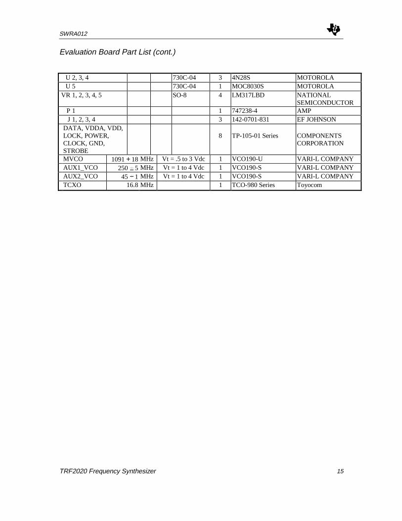
Table 1. Evaluation Board Part List
REF DESIGNATOR VALUE SIZE QTY MANU P/N MANUFACTURER
C 1 4.7 uF "A" 3.2x1.6 1 TA010TCM475KAR VENKEL
C 2,3,4, 5, 25 1.0 uF "A" 3.2x1.6 5 TA025TCM105KAR VENKELC 6, 19 4700 pF 0603 1.6x.08 2 GRM39X7R Series muRATAC 7, 12, 20, 22, 39,
40, 41, 42, 44, 51,52, 61
0.1 uF 0603 1.6x.08 12 GRM39X7R Series muRATA
C 8,46 100 pF 0603 1.6x.08 2 GRM39X7R Series muRATAC 13 820 pF 0603 1.6x.08 1 GRM39X7R Series muRATAC 14 47 pF 0603 1.6x.08 1 GRM39X7R Series muRATAC 15 DNP 0603 1.6x.08 1 NOT USEDC 16 68 pF 0603 1.6x.08 1 GRM39X7R Series muRATAC 18 680 pF 0603 1.6x.08 1 GRM39X7R Series muRATAC 23 22 nF 0603 1.6x.08 1 GRM39X7R Series muRATAC 24, 43, 45, 48 220 pF 0603 1.6x.08 4 GRM39X7R Series muRATAC 55 33 pF 0603 1.6x.08 1 GRM39X7R Series muRATAC 57 330 pF 0603 1.6x.08 1 GRM39X7R Series muRATAC 58 12 nF 0603 1.6x.08 1 GRM39X7R Series muRATAC 59, 60, 63, 64 22 pF 0603 1.6x.08 4 GRM39X7R Series muRATAC 62 1000 pF 0603 1.6x.08 1 GRM39X7R Series
R 1,2 220 : 0603 1.6x.08 2 ERJ-3GSYJ Series PANASONICR 3, 13, 37 270 : 0603 1.6x.08 3 ERJ-3GSYJ Series PANASONICR 5, 6 1 k: .25" SQUARE 2 ERJ-3GSYJ Series BOURNSR 7, 38 820 : 0603 1.6x.08 2 ERJ-3GSYJ Series PANASONICR 8 390 : 0603 1.6x.08 1 ERJ-3GSYJ Series PANASONICR 9, 43 24 k: 0603 1.6x.08 2 ERJ-3GSYJ Series PANASONICR 10, 25, 46 49.9 : 0603 1.6x.08 3 ERJ-3EKF49R9 PANASONICR 11, 12, 15, 23, 24,
26, 47, 49, 5018 : 0603 1.6x.08 9 ERJ-3GSYJ Series PANASONIC
R 17 33 k: 0603 1.6x.08 1 ERJ-3GSYJ Series PANASONICR 18,20, 54 12.0 k: 0603 1.6x.08 3 ERJ-3GSYJ Series PANASONICR 19 36 k: 0603 1.6x.08 1 ERJ-3GSYJ Series PANASONICR 21 20 k: 0603 1.6x.08 1 ERJ-3GSYJ Series PANASONICR 22 18 k: 0603 1.6x.08 1 ERJ-3GSYJ Series PANASONICR 27,28,29,34 1.8 k: 0603 1.6x.08 4 ERJ-3GSYJ Series PANASONICR 30 2.7 k: 0603 1.6x.08 1 ERJ-3GSYJ Series PANASONICR 31,32,33 3.6 k: 0603 1.6x.08 3 ERJ-3GSYJ Series PANASONICR 56 51 k: 0603 1.6x.08 1 ERJ-3GSYJ Series PANASONICR 59 15 k: 0603 1.6x.08 1 ERJ-3GSYJ Series PANASONIC
U 1 1 TRF 2050 TEXASINSTRUMENTS
SWRA012
TRF2020 Frequency Synthesizer 15
Evaluation Board Part List (cont.)
U 2, 3, 4 730C-04 3 4N28S MOTOROLAU 5 730C-04 1 MOC8030S MOTOROLA
VR 1, 2, 3, 4, 5 SO-8 4 LM317LBD NATIONALSEMICONDUCTOR
P 1 1 747238-4 AMPJ 1, 2, 3, 4 3 142-0701-831 EF JOHNSON
DATA, VDDA, VDD,LOCK, POWER,CLOCK, GND,STROBE
8 TP-105-01 Series COMPONENTSCORPORATION
MVCO 1091 r 18 MHz Vt = .5 to 3 Vdc 1 VCO190-U VARI-L COMPANYAUX1_VCO 250 r 5 MHz Vt = 1 to 4 Vdc 1 VCO190-S VARI-L COMPANYAUX2_VCO 45 r 1 MHz Vt = 1 to 4 Vdc 1 VCO190-S VARI-L COMPANYTCXO 16.8 MHz 1 TCO-980 Series Toyocom
SWRA012
16 TRF2020 Frequency Synthesizer
2.1. Voltage Regulators
The on-board regulators provide independent, linear voltageregulation to the TRF2020, the Main VCO, the Auxiliary VCOs,and the serial interface opto-couplers. Regulators VR1 (VDDA)and VR2 (VDD) are adjustable using variable resistors R5 and R6respectively. VR3 (VOSC1), VR4 (VOSC2) and VR5 (OPTO) canbe adjusted by changing the combination of the resistor pairsR3/R7, R8/R13 and R37/R38. Tantalum capacitors are used toenhance ripple and noise rejection in the regulators.
The voltage regulators are factory set as follows:
VR1 - 3.0 VDC ..... VDDA
VR2 - 3.0 VDC ..... VDD
VR3 - 5.0 VDC ..... VOSC1
VR4 - 3.2 VDC ..... VOSC2
VR5 - 5.0 VDC ..... VOPTO
2.2. External Power
External power is connected to the evaluation board at the testpoints SUPPLY and GND. It is recommended that a linear powersupply set between +7Vdc to +9Vdc is used for external power.
2.3. Serial Interface
A DB25M connector is provided for connection to a standard PCparallel port using a 25-conductor cable. The PC parallel port isused to emulate a synchronous serial data interface consisting ofCLOCK, DATA, and STROBE. The LOCK signal is fed back tothe PC parallel port to indicate synthesizer loop lock status of theTRF2020. The three serial interface signals and the LOCK signalare all opto-isolated from the PC parallel port. In this manner, theTRF2020 device may be operated at a supply voltage that isdifferent than the standard +5 VDC voltage level of the PC parallelport.
The serial interface signals are routed to the DB25M connector asfollows:
CLOCK - Pin 2,
DATA - Pin 3,
STROBE - Pin 4,
LOCK - Pin 10.

SWRA012
TRF2020 Frequency Synthesizer 17
2.4. External Reference
The factory installed TCXO (Temperature Compensated CrystalOscillator) can be removed and an external reference signalsource can be connected to J4 (REF_IN) for operation atreference frequencies other than the one at which the TCXOoperates. Typically, a low phase noise, stable, synthesized signalgenerator such as an HP8665 or similar would be used as anexternal reference. For typical GSM applications, a 13.00 MHzsignal at – 6 dBm is suitable. A 16.8MHz TCXO has beeninstalled.

SWRA012
18 TRF2020 Frequency Synthesizer
3. Software Driver
A DOS based software driver is supplied with the evaluationboard. The software is intended for use in a MS-DOSenvironment. No special memory is required to use the software.Two files are contained on the provided disk: TRF2020.EXE andINIT.CFG. Both of these files should be placed in the samedirectory on a hard disk or the program may be executed from thedisk provided. To execute the program from the provided disk,simply type the following
A:\ � (Enter)
TRF2020 � (Enter)
The program executes from the TRF2020.EXE file. The INIT.CFGfile is read by the program to setup the program parameters. TheINIT.CFG file may be changed to suit your needs; see F9 SaveFile description.
3.1. Program Screen
The program screen is divided into five main sections: Main Loop,Auxiliary Loop #1, Auxiliary Loop #2, Device and EditingParameters. The Main Loop section displays all of the pertinentparameters concerning the main synthesizer. The Auxiliary Loopsections display all of the pertinent parameters concerning theauxiliary synthesizers. The Device section displays all of thepertinent parameters concerning the device enables, modes, andreference frequency. And the bottom two lines of the displaysuggests appropriate keys to use or actions to take based on theuser inputs
3.1.1. Main Loop Section
The main loop section displays the current main synthesizer loopparameters. All parameters displayed in the main loop sectioncan be modified except the Phase Detector Freq, which isinformative only. The Phase Detector Freq parameters arecalculated from the reference frequency (Refrnc Freq) andreference counter (Refrnc Count P) parameters in the Devicesection.

SWRA012
TRF2020 Frequency Synthesizer 19
3.1.1.01. VCO Frequency
The main VCO Frequency parameter is not actually a TRF2020device parameter, but it may be used to cause the program toautomatically find a solution, if possible, for NM1-NM2 based onthe entered VCO frequency parameter and others. The correctreference frequency (Refrnc Freq), and the reference count (P)should be entered before using the VCO Frequency parameter tocalculate a channel solution.
3.1.1.02. Speedup Time C
The C field selects the duration of speedup mode for the mainsynthesizer. The duration of speedup mode is determined asfollows:
frequency Reference
2 =Duration
C,
where reference frequency is typically 200 kHz for GSM or 30 kHzfor AMPS.
3.1.1.03. Current Ratio F
The F field selects the desired main synthesizer speed-up/normalmode current ratio.
The choices are:
F = 3 8 (2 mA/0.25 mA),
F = 2 4 (2 mA/0.5 mA),
F = 1 2 (2 mA/1 mA),
F = 0 1 (2 mA/2 mA).
3.1.1.04. Enable Loop R
The R field enables/disables the main synthesizer as follows:
R = 0 enabled,
R = 1 disabled.
3.1.1.05. NM1-2 B and A
The B and A fields can be programmed manually to any validnumber. These fields are also automatically updated when theVCO Frequency field is used to enter a valid main synthesizerchannel frequency.

SWRA012
20 TRF2020 Frequency Synthesizer
3.1.1.06. Reference Post Select L
The L field selects the main synthesizer reference postscalerselect as follows:
L = 0 Reference/1,
L = 1 Reference/2,
L = 2 Reference/4,
L = 3 Reference/8.
3.1.2. Auxiliary-1 Loop Section
The auxiliary-1 loop section displays the current auxiliary-1 loopparameters. All parameters displayed in the auxiliary-1 loopsection can be modified except for Phase Detector Freq. Thisparameter is calculated from the reference frequency (RefrncFreq) and reference counter (Refrnc Count P) parameters in theDevice section.
3.1.2.01. VCO Frequency
The auxiliary-1 VCO Frequency parameter is not actuallyTRF2020 device parameter but may be used to cause theprogram to automatically find a solution, if possible, for NM1-2based on the entered VCO frequency parameter and others. Thecorrect reference frequency (Refrnc Freq) and the reference count(P) should be entered before using the VCO Frequency parameterto calculate a channel solution.
3.1.2.02. Speedup Time G
The G field selects the duration of speedup mode for bothauxiliary-1 and auxiliary-2 synthesizers. The duration of speedupmode is determined as follows:
frequency Reference
2 =Duration
G,
where the reference frequency is typically 200kHz for GSM and30kHz for AMPS.

SWRA012
TRF2020 Frequency Synthesizer 21
3.1.2.03. Current Ratio K
The K field selects the desired speed-up/normal mode currentratio for both auxiliary-1 and auxiliary-2 synthesizers. The choicesare:
K = 3 8 (2 mA/0.25 mA),
K = 2 4 (2 mA/0.5 mA),
K = 1 2 (2 mA/1 mA),
K = 0 1 (2 mA/2 mA).
3.1.2.04. Enable Loop S
The S field enables/disables the auxiliary-1 synthesizer as follows:
S = 0 enabled,
S = 1 disabled.
3.1.2.05. NM1-2 E and D
The E and D fields can be programmed manually to any validnumber. These fields are also automatically updated when theVCO Frequency field is used to enter a valid auxiliary-1synthesizer channel frequency.
3.1.2.06. Reference Post Select M
The M field selects the main synthesizer reference postscalerselect as follows:
M = 0 Reference/1,
M = 1 Reference/2,
M = 2 Reference/4,
M = 3 Reference/8.
3.1.3. Auxiliary-2 Loop Section
The auxiliary-2 loop section displays the current auxiliary-2 loopparameters. All parameters displayed in the auxiliary-2 loopsection can be modified except for Phase Detector Freq. Thisparameter is calculated from the reference frequency (RefrncFreq) and reference counter (Refrnc Count P) parameters in theDevice section.

SWRA012
22 TRF2020 Frequency Synthesizer
3.1.3.01. VCO Frequency
The auxiliary-2 VCO Frequency parameter is not actually aTRF2020 device parameter but may be used to cause theprogram to automatically find a solution, if possible, for NM1-2based on the entered VCO frequency parameter and others. Thecorrect reference frequency (Refrnc Freq) and the reference count(NR) should be entered before using the VCO Frequencyparameter to calculate a channel solution.
3.1.3.02. Speedup Time G
See 3.1.2.02 section
3.1.3.03. Current Ratio K
See 3.1.2.03 section
3.1.3.04. Enable Loop T
The T field enables/disables the auxiliary-2 synthesizer as follows:
T = 0 enabled,
T = 1 disabled.
3.1.3.01. NM1-2 J and H
The J and H fields can be programmed manually to any validnumber. These fields are also automatically updated when theVCO Frequency field is used to enter a valid auxiliary-2synthesizer channel frequency.
3.1.3.01. Reference Post Select N
The N field selects the main synthesizer reference postscaler asfollows:
N = 0 Reference/1,
N = 1 Reference/2,
N = 2 Reference/4,
N = 3 Reference/8.
3.1.4. Device Section
The device section displays the current device parameters. Allparameters displayed in the device section can be modifiedexcept Synthesizer Status , which is a read-back from the Lockterminal on the TRF2020 device.

SWRA012
TRF2020 Frequency Synthesizer 23
3.1.4.01. Lock Detect U
The lock detect U field selects the function of the lock detectcircuitry as follows:
U = 0 Main,
U = 1 Aux-1,
U = 2 Aux-2,
U = 3 AND-ed.
3.1.4.02. Device Test V
The device test V field is reserved evaluation and should normallyremain set to zero. When this field is set to zero, the LOCKterminal is operating normally. Otherwise, the LOCK terminal isconnected to internal nodes in the TRF2020.
3.1.4.03. Reference Frequency (Refrnc Freq)
The external reference frequency or installed TCXO frequencyused with the evaluation board should be entered in this locationin order that other parameters such as the phase detectorreference frequency can be properly calculated and displayed.
3.1.4.04. Reference Count P
The P field selects the division ratio of the reference frequencycounter.
3.1.4.05. Synthesizer Status
The Synthesizer Status is a read-back only field that reflects thecurrent status of the LOCK terminal.
3.1.5. Editing parameters
To edit any one of the program parameters displayed, the userfirst selects an appropriate function key (described below) toselect a section of the display such as the Main Loop section. Thearrow (m, n, o, p) and Tabulation (TAB) keys are used to movethe cursor to the parameter to be edited. Once the cursor islocated at the proper location, press Enter (or Return) to select theparameter. Next, enter the new value and press Enter again.Once all of the parameters within a particular section of thedisplay have been edited as desired, press the Escape (ESC) keyto return to the main menu. For example, to edit the Post Selectparameter in the Main Loop section from the main menu, thefollowing keystrokes are performed:
SWRA012
24 TRF2020 Frequency Synthesizer
�� F1 to select the Main Loop section
�� o to move to the right column
���� p to move down the right column
���� p to move down the right column
���� Enter to select the Post Select field
�� Data enter the desired data such as 2
�� Enter to complete the field edit
�� ESC to leave the Main Loop section and return to the
main menu
3.1.5.01. Function Keys
Function keys are used to select sections of the display for editingpurposes or to perform a program function as follows:
F1: Edit PLL Main - Selects the Main Loop section of the displayfor editing.
F2: Edit PLL Aux-1 - Selects the Auxiliary-1 Loop section of thedisplay for editing.
F3: Edit PLL Aux-2 - Selects the Auxiliary-2 Loop section of thedisplay for editing.
F4: Edit Device - Selects the Device section of the display forediting.
F5: View Bit Map - Used to view the current multi-word bitmap.
F7: Select Port - Used to select the PC parallel port. This function“looks” at the ROM BIOS to find all parallel ports. Follow thedirections to select a particular port if more than one is found.
F8: Load File - Used to load a configuration file to reset theprogram parameters to a user specified condition. This functionwill look for the entered file on the same disk and in the samedirectory from which the program is executing. Any existing,allowable DOS name can be used. The INIT.CFG file may alsobe loaded using this function to restore to original programconfiguration.

SWRA012
TRF2020 Frequency Synthesizer 25
F9: Save File - Used to save a configuration file containing thecurrent program parameters to a user-specified file. This functionwill write the program parameters to the specified file name on thesame disk and in the same directory from which the program isexecuting. Any allowable DOS name can be used. The INIT.CFGfile may also be re-written using this function to change the bootprogram configuration.
F10: Send to Device - Used to program the TRF2020 device.When F10 is selected, the current bitmap is displayed and theuser enters the letter (A, B, C, D, E, G) of the word to be sent tothe TRF2020. The default sequence of G, D, C, B, and A in ordercan be sent to the TRF2020 by simply pressing Enter without firstselecting a letter.
3.1.5.02. Quitting the Program
CTL-Q: Quit - The Control (Ctrl) key is depressed and held whilethe Q key is pressed to exit the program and return to DOS.
SWRA012
26 TRF2020 Frequency Synthesizer
Evaluation Board Disclaimer
Please note that the enclosed evaluation boards are experimentalPrinted Circuit Boards and are therefore only intended for deviceevaluation.
We would like to draw your attention to the fact that these boardshave been processed through one or more of Texas Instruments’external subcontractors who have not been production qualified.
Device parameters measured, using these boards, are notrepresentative of any final datasheet or of a final productionversion. Texas Instruments does not represent or guarantee thata final version will be made available after device evaluation.
THE EVALUATION BOARDS ARE SUPPLIED WITHOUT WARRANTYOF ANY KIND, EXPRESSED, IMPLIED OR STATUTORY, INCLUDINGBUT NOT LIMITED TO, ANY IMPLIED WARRANTY OFMERCHANTABILITY OR FITNESS FOR A PARTICULAR PURPOSE.
TEXAS INSTRUMENTS ACCEPTS NO LIABILITY WHATSOEVERARISING AS A RESULT OF THE USE OF THESE BOARDS.