lmx2531lq1312 high perf frequency synthesizer with int vco
TRANSCRIPT

LMX2531LQ1312E Evaluation Board Operating Instructions
National Semiconductor Corporation Timing Devices Business Group
10333 North Meridian
Suite 400 Indianapolis, IN 46290
LMX2531LQ1312EFPEB Rev 4.02.2008

L M X 2 5 3 1 L Q 1 3 1 2 E E V A L U A T I O N B O A R D O P E R A T I N G I N S T R U C T I O N S
Table of Contents TABLE OF CONTENTS ................................................................................................................................... 2 LOOP FILTER................................................................................................................................................ 3 QUICK SETUP ............................................................................................................................................... 3 TROUBLESHOOTING ..................................................................................................................................... 4 PHASE NOISE ............................................................................................................................................... 5 FREE-RUNNING VCO NOISE (INTERNAL DIVIDE BY 2 DISABLED)............................................................... 6 FREE-RUNNING VCO NOISE (INTERNAL DIVIDE BY 2 ENABLED)................................................................ 7 FRACTIONAL SPURS (INTERNAL DIVIDE BY 2 DISABLED) ............................................................................ 8 FRACTIONAL SPURS (INTERNAL DIVIDE BY 2 ENABLED) ............................................................................. 9 INTEGER SPURS (INTERNAL DIVIDE BY 2 ENABLED).................................................................................. 10 INTEGER SPURS (INTERNAL DIVIDE BY 2 ENABLED).................................................................................. 11 CODELOADER SETTINGS............................................................................................................................ 12 SCHEMATIC................................................................................................................................................ 17 BILL OF MATERIALS................................................................................................................................... 18 TOP LAYER ................................................................................................................................................ 19 MID LAYER 1 "GROUND PLANE" ............................................................................................................... 20 MID LAYER 2 "POWER" ............................................................................................................................. 21 BOTTOM LAYER "SIGNAL"......................................................................................................................... 22 TOP BUILD DIAGRAM................................................................................................................................. 23
2

L M X 2 5 3 1 L Q 1 3 1 2 E E V A L U A T I O N B O A R D O P E R A T I N G I N S T R U C T I O N S
Loop Filter
Loop Bandwidth 7.7 kHz Kφ 1440 uA (16X) Phase Margin 61.5 deg Fcomp 10 MHz
Crystal Frequency 10 MHz Output Frequency 1268 – 1360 MHz (DIV2=0) 634 - 680 MHz (DIV2=1)
Supply Voltage 3.0 Volts VCO Gain 3 - 6 MHz/Volt
VCOCPout
open 10
0 nF
1KΩ
100 pF 100 pF
20 KΩ 20 KΩ
Vtune
Quick Setup
• Install the CodeLoader software which is available at www.national.com/timing. • Attach the parallel or USB to parallel, port cable to the computer and the evaluation board. • Connect 3.0 volts to the Vcc connector • Connect the Fout connector to a spectrum analyzer or phase noise analyzer • Connect a clean 10 MHz source to the OSCin pin. Typically, the 10 MHz output from the back
of the RF test equipment is a good source. Signal generators tend to be very noisy and should be used with caution. If a signal generator is used, the signal generator phase noise contribution can be reduced by setting the signal to 80 MHz and dividing this down to a phase detector frequency of 10 MHz.
• Set up the CodeLoader software o Select the proper part from the menu as Select Part>PLL+VCO>LMX2531LQ1312E o Select the proper mode from the Mode menu o Load the part by pressing (Ctrl+L) or selecting Keyboard Controls->Load Device from
the menu • It is recommended to ensure proper communication with the device
o Click the REG_RST bit on the bits/pins page and observe the current go to 0 mA o Unclick the REG_RST bit AND press (Ctrl+L). The current should be approximately 35 mA o If device does not respond to this, consult the troubleshooting section
• When using the lower frequency band with divide by 2 enabled (DIV2=1), be aware that the frequency programmed to the VCO is actually twice the output frequency of the device because the VCO frequency is being divided by 2.
3

L M X 2 5 3 1 L Q 1 3 1 2 E E V A L U A T I O N B O A R D O P E R A T I N G I N S T R U C T I O N S
Troubleshooting Problem Corrective Actions
Softw
are
does
not
com
mun
icat
e w
ith t
he e
valu
atio
n bo
ards
All Modes
• Ensure a valid signal is presented to the OSCin connector. If a signal generator is used, ensure the RF is ON.
• Consult the CodeLoader instructions for more detailed information on communication issues. (See www.national.com/timing)
LPT Mode (Uses Parallel Port Cable) • Ensure that CodeLoader is selected to LPT mode on the Port Setup tab. • Ensure the proper port number is selected (LPT1, LPT2, LPT3). CodeLoader does
NOT automatically detect this. • Ensure the LPT cable is securely connected to the computer and board. • Try to exit and restart CodeLoader. • Ensure the parallel port is in the correct mode
o Windows often requires administrative access to write to the parallel port. o Ensure that the parallel port is set to “Enabled” in windows device manager. o A reboot upon installation of CodeLoader is sometimes necessary to get the
parallel port to work. o Standard mode is the most reliable. This can be set in the BIOS mode of the
computer as “Normal”, “Output Only”, or “AT”. USB Mode (USB to Parallel Port Converter)
• On the menu, select USB>Version to verify communication with the board. • Ensure the Green LEDs are lit on the USB board. • Ensure there are no conflicts with other USB devices and reinstall the board.
Part
resp
onds
to
prog
ram
min
g, b
ut
does
not
loc
k to
he
co
rrec
t t fre
quen
cy
• Ensure there is a valid signal presented to the OSCin connector. If a signal generator is used, the RF should be set to ON.
• If using the lower frequency band (DIV2=1), understand that the VCO frequency in CodeLoader should be twice the frequency at the Fout pin.
• Ensure that the VCO FREQUENCY CAL bits on the Bits/Pins tab are correct. • Ensure the loop filter is optimized if the charge pump current, phase detector frequency,
or loop filter values have been changed from their original settings. Ensure the integrated loop filter components on CodeLoader are set to their proper settings.
Clo
se-in
ph
ase
nois
e is
w
orse
th
an
eval
uatio
n bo
ard
inst
ruct
ions
show
• Ensure the signal presented to OSCin connector is clean. Try another source, or if it is a signal generator, try using a higher frequency and dividing it down to the phase detector frequency.
• Ensure the OSCin signal and cable provides sufficient power level. • If the phase detector frequency or charge pump current is lowered from their original
settings, the in-band phase noise can be degraded, even if the loop filter is re-designed for the same loop bandwidth. If the loop bandwidth is decreased, in-band phase noise can be degraded.
Far-o
ut
Phas
e no
ise
is
wor
se
than
ev
alua
tion
boar
d in
stru
ctio
nssh
ow
• Ensure the measurement equipment noise floor is not limiting the measurement. For spectrum analyzers, the noise floor at a particular setting can be measured by removing the RF input signal.
• If the settings are changed from what the board was designed for, ensure the delta-sigma modulator is not increasing the far-out noise. To know this, tune to an integer channel and set the ORDER bit to “Reset Modulator”. The far-out phase noise should not decrease. If it does, try a loop filter with more attenuation or select a lower order delta-sigma modulator.
4

L M X 2 5 3 1 L Q 1 3 1 2 E E V A L U A T I O N B O A R D O P E R A T I N G I N S T R U C T I O N S
Phase Noise O
utpu
t Fre
quen
cy =
131
4 M
Hz
Inte
rnal
Div
ide
by 2
Dis
able
d (D
IV2=
0)
Out
put F
requ
ency
= 6
57 M
Hz
Inte
rnal
Div
ide
by 2
Ena
bled
(DIV
2=1)
5

L M X 2 5 3 1 L Q 1 3 1 2 E E V A L U A T I O N B O A R D O P E R A T I N G I N S T R U C T I O N S
Free-Running VCO Noise (Internal Divide by 2 Disabled)
Fout
= 1
268
MH
z Fo
ut =
131
4 M
Hz
Fout
= 1
360
MH
z
The plots to the left show the
true phase noise capability of
the VCO. In order to take
these plots, the E5052 phase
nose analyzer was used. The
method was to lock the PLL to
the proper frequency, then
disable the EN_PLL,
EN_PLLLDO1, and
EN_PLLLDO2 bits. The
equipment needs to be able to
track the VCO phase noise to
measure in this way, and one
can not let the VCO drift too
far off in frequency. If this kind
of equipment is not available,
the VCO phase noise can also
be measured by making a
very narrow loop bandwidth
filter.
On the 1312E option
especially of the LMX2531
family, pay special attention to
bypassing at the VregPLL1,
VregPLL2, and VregVCO
pins. This option is especially
sensitive to this. Phase noise
degradation in the 10 – 200
kHz range can happen. Even
on these plots, there is some
room for optimization.
6

L M X 2 5 3 1 L Q 1 3 1 2 E E V A L U A T I O N B O A R D O P E R A T I N G I N S T R U C T I O N S
Free-Running VCO Noise (Internal Divide by 2 Enabled)
Fout
= 6
34 M
Hz
(126
8 M
Hz/
2)
Fout
= 6
57 M
Hz
(131
4 M
Hz/
2)
Fout
= 6
80 M
Hz
(136
0 M
Hz/
2)
The plots to the left show the
true phase noise capability of
the VCO. In order to take
these plots, the E5052 phase
noise analyzer was used.
The method was to lock the
PLL to the proper frequency,
then disable the EN_PLL,
EN_PLLLDO1, and
EN_PLLLDO2 bits. The
equipment needs to be able to
track the VCO phase noise to
measure in this way, and one
can not let the VCO drift too
far off in frequency. If this kind
of equipment is not available,
the VCO phase noise can also
be measured by making a
very narrow loop bandwidth
filter.
When divide by 2 is enabled,
the phase noise at lower
offsets is about 6 dB better. At
high offsets, the overall phase
noise improvement may be
lower because the divider is
noise floor is adding to the
phase noise.
7
L M X 2 5 3 1 L Q 1 3 1 2 E E V A L U A T I O N B O A R D O P E R A T I N G I N S T R U C T I O N S
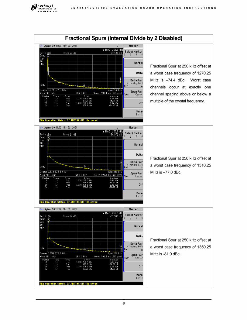
Fractional Spurs (Internal Divide by 2 Disabled)
Fractional Spur at 250 kHz offset at
a worst case frequency of 1270.25
MHz is –74.4 dBc. Worst case
channels occur at exactly one
channel spacing above or below a
multiple of the crystal frequency.
Fractional Spur at 250 kHz offset at
a worst case frequency of 1310.25
MHz is –77.0 dBc.
Fractional Spur at 250 kHz offset at
a worst case frequency of 1350.25
MHz is -81.9 dBc.
8

L M X 2 5 3 1 L Q 1 3 1 2 E E V A L U A T I O N B O A R D O P E R A T I N G I N S T R U C T I O N S
Fractional Spurs (Internal Divide by 2 Enabled)
Spur at 250 kHz offset at a
frequency of 635.125 MHz is –84.2
dBc. Since this mode uses the
divide by 2 mode, the channel
spacing here is actually 125 kHz. If
there was a fractional spur at 125
kHz, it could be eliminated by
doubling the channel spacing
before the divider.
Spur at 250 kHz offset for a
frequency of 655.125 MHz is -83.2
dBc.
Spur at 250 kHz offset for a
frequency of 675.125 MHz is –88.4
dBc. The sub-fractional spur at 125
kHz offset of -89.7 dBc is also
visible.
9
L M X 2 5 3 1 L Q 1 3 1 2 E E V A L U A T I O N B O A R D O P E R A T I N G I N S T R U C T I O N S
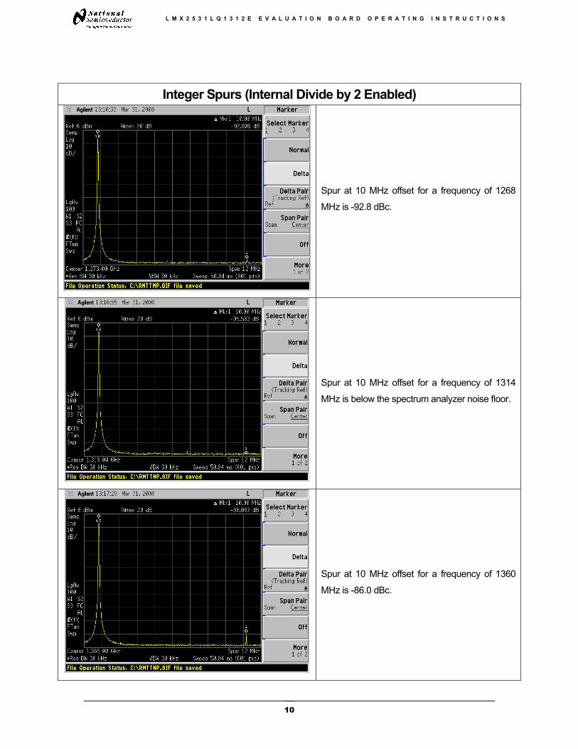
Integer Spurs (Internal Divide by 2 Enabled)
Spur at 10 MHz offset for a frequency of 1268
MHz is -92.8 dBc.
Spur at 10 MHz offset for a frequency of 1314
MHz is below the spectrum analyzer noise floor.
Spur at 10 MHz offset for a frequency of 1360
MHz is -86.0 dBc.
10
L M X 2 5 3 1 L Q 1 3 1 2 E E V A L U A T I O N B O A R D O P E R A T I N G I N S T R U C T I O N S
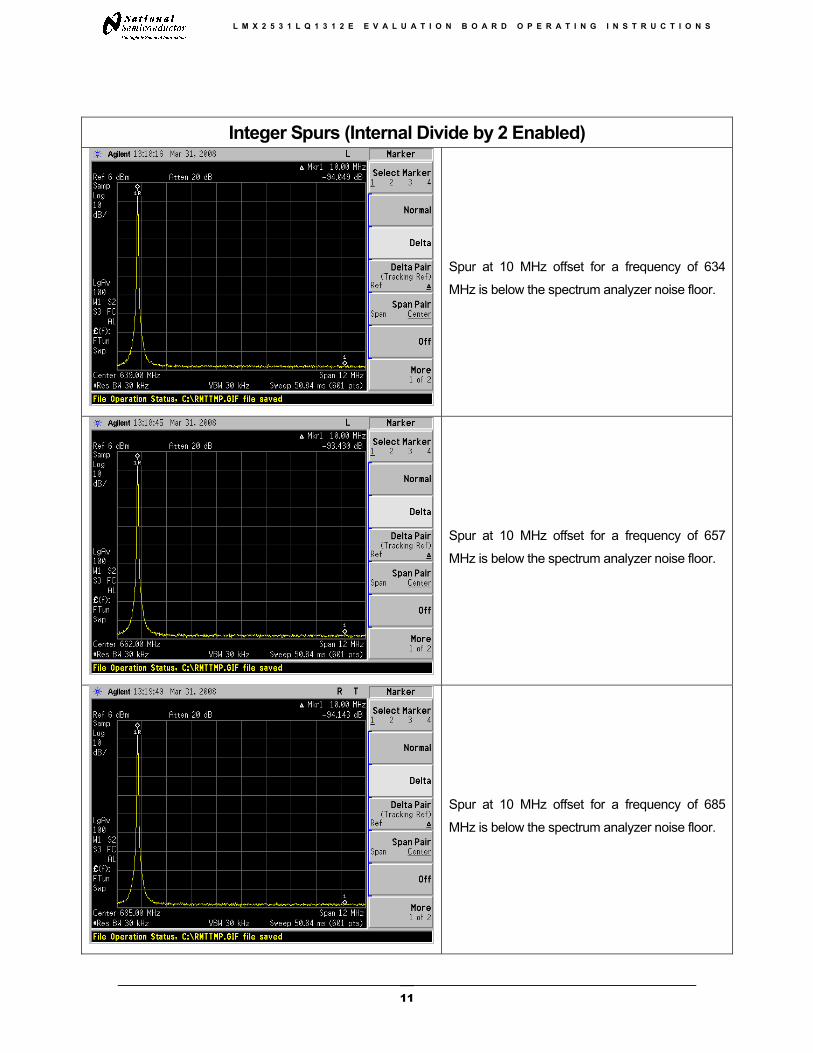
Integer Spurs (Internal Divide by 2 Enabled)
Spur at 10 MHz offset for a frequency of 634
MHz is below the spectrum analyzer noise floor.
Spur at 10 MHz offset for a frequency of 657
MHz is below the spectrum analyzer noise floor.
Spur at 10 MHz offset for a frequency of 685
MHz is below the spectrum analyzer noise floor.
11

L M X 2 5 3 1 L Q 1 3 1 2 E E V A L U A T I O N B O A R D O P E R A T I N G I N S T R U C T I O N S
CodeLoader Settings
The CodeLoader program is designed to work with many devices. When CodeLoader is first started, it is necessary to s
elect the correct device.
12
L M X 2 5 3 1 L Q 1 3 1 2 E E V A L U A T I O N B O A R D O P E R A T I N G I N S T R U C T I O N S
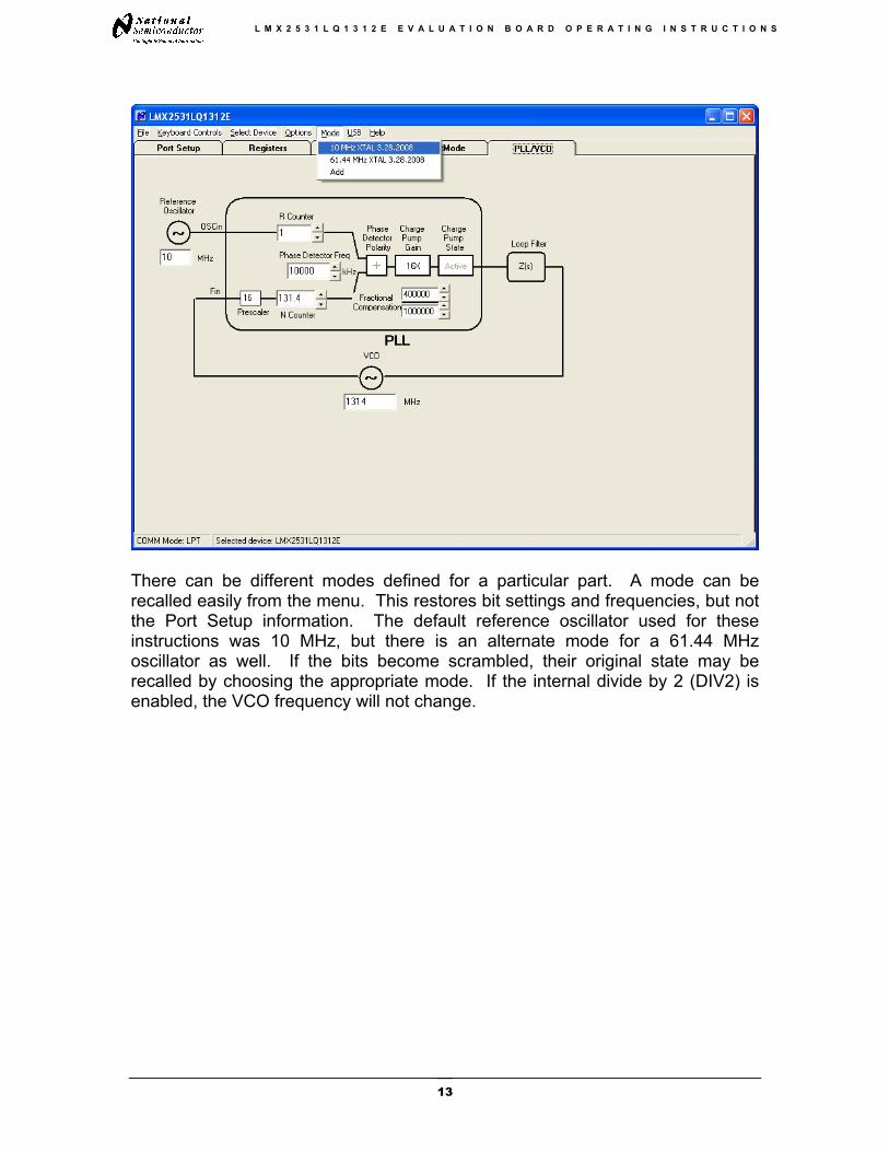
There can be different modes defined for a particular part. A mode can be recalled easily from the menu. This restores bit settings and frequencies, but not the Port Setup information. The default reference oscillator used for these instructions was 10 MHz, but there is an alternate mode for a 61.44 MHz oscillator as well. If the bits become scrambled, their original state may be recalled by choosing the appropriate mode. If the internal divide by 2 (DIV2) is enabled, the VCO frequency will not change.
13
L M X 2 5 3 1 L Q 1 3 1 2 E E V A L U A T I O N B O A R D O P E R A T I N G I N S T R U C T I O N S
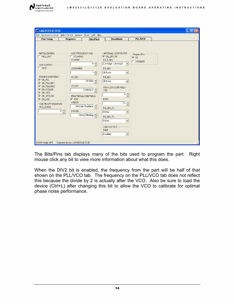
The Bits/Pins tab displays many of the bits used to program the part. Right mouse click any bit to view more information about what this does. When the DIV2 bit is enabled, the frequency from the part will be half of that shown on the PLL/VCO tab. The frequency on the PLL/VCO tab does not reflect this because the divide by 2 is actually after the VCO. Also be sure to load the device (Ctrl+L) after changing this bit to allow the VCO to calibrate for optimal phase noise performance.
14

L M X 2 5 3 1 L Q 1 3 1 2 E E V A L U A T I O N B O A R D O P E R A T I N G I N S T R U C T I O N S
The Registers tab shows the literal bits that are being sent to the part. These are the registers every time the PLL is loaded by using the menu command or
trl+L). R5 (INIT1) and R5 (INIT 2) are just the R5 register being used to (Cproperly initialize the part. So a single (Ctrl+L) will load the part.
15

L M X 2 5 3 1 L Q 1 3 1 2 E E V A L U A T I O N B O A R D O P E R A T I N G I N S T R U C T I O N S
The port setup tells CodeLoader what information goes where. If this is wrong, the part will not program. Although LPT1 is usually correct, CodeLoader does NOT automatically detect the correct port. On some laptops, it may be LPT3. Manually verification is required.
16

L M X 2 5 3 1 L Q 1 3 1 2 E E V A L U A T I O N B O A R D O P E R A T I N G I N S T R U C T I O N S
17
L M X 2 5 3 1 L Q 1 3 1 2 E E V A L U A T I O N B O A R D O P E R A T I N G I N S T R U C T I O N S
17
Schematic
1 2 3 4 5 6
A
B
C
D
654321
D
C
B
A
Title
Number RevisionSize
B
Date: 6-Jan-2006 Sheet of File: C:\Documentum\Checkout\LMX2531LQEBPCB.ddb.ddbDrawn By:
R6
R16 R15 R13 R12 R11
R2_
LF
R8
C7
C2p
LF
C2_
LF C1_
LF
R14
LMX2531 Evaluation Board
LMX2531SLBCBPCB 01-06-2006
Dan Chappel l
C8
12
34
56
78
910
uWIRE
R10
C6
R2p
LF
C16
FRAME
Fout
Vcc
R21R19
R20
C1
R2
C12
C2
VccVCO
VccDIG
VccPLL
VccBUFR3
C3
C17
R4
C9
C4
R5
C5
OSCin
VccVCO
VccPLL
VccBUF
C13
C18
C20
R7
R23
R22
Ftest/LD
C15
C22
R1
R9
TRIGGER
GND
1 23 45 67 8
POWER
C24
C14
C11
C19
C21
C23
Note that Any Component with Designator 100 or Higher is on the Bottom Side of the Board
C10
VccDIG
BUF
1
NC2
GND3
NC4
NC5
Vreg6
NCDATACLK
789
LE
10
CE
11
NC
12
NC
13
NC
14
NC
15
Vcc
VC
O16
Vre
gVC
O17
Vre
fVC
O18
GND 19GND 20Fout 21VccBUF 22Vtune 23CPout 24FLout 25VregPLL1 26VccPLL 27
GN
D34
NC
29Ft
est/L
D30
OSC
in31
OSC
in*
32T
est
33
NC
35V
regD
IG36
Vre
gPL
L228
SLG
137
SLG
238
SLG
339
U1
Vcc
Vcc
R18
R24
R17
C10
5
C10
0
C10
1
C10
3
C10
4C
102
VccDIG
L M X 2 5 3 1 L Q 1 3 1 2 E E V A L U A T I O N B O A R D O P E R A T I N G I N S T R U C T I O N S
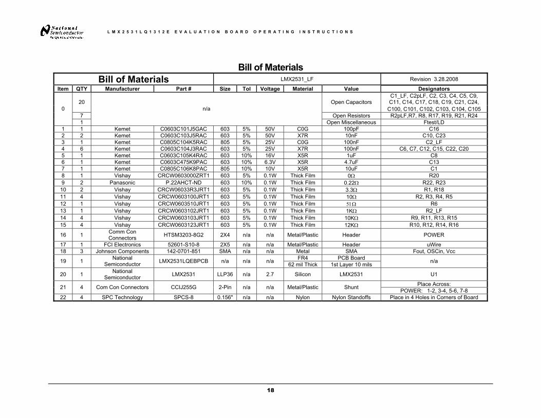
Bill of Materials Bill of Materials LMX2531_LF Revision 3.28.2008
Item QTY Manufacturer Part # Tol Voltage Material Value Designators Size C1_LF, C2pLF, C2, C3, C4, C5, C9, C11, C14, C17, C18, C19, C21, C24, 20 Open Capacitors
C100, C101, C102, C103, C104, C105 7 Open Resistors R2pLF,R7, R8, R17, R19, R21, R24
0
1
n/a
Open Miscellaneous Ftest/LD 1 1 Kemet C0603C101J5GAC 603 5% 50V C0G 100pF C16 2 2 Kemet C0603C103J5RAC 603 5% 50V X7R 10nF C10, C23 3 1 Kemet C0805C104K5RAC 805 5% 25V C0G 100nF C2_LF 4 6 Kemet C0603C104J3RAC 5% 25V X7R 100nF C6, C7, C12, C15, C22, C20 603 5 1 Kemet C0603C105K4RAC 603 10% 16V X5R 1uF C8 6 1 Kemet C0603C475K9PAC 603 10% 6.3V X5R 4.7uF C13 7 1 Kemet C0805C106K8PAC 805 10% 10V X5R 10uF C1 8 1 Vishay CRCW0603000ZRT1 603 5% 0.1W Thick Film 0 R20 Ω 9 2 Panasonic P.22AHCT-ND 603 10% 0.1W Thick Film 0.22Ω R22, R23
10 2 Vishay CRCW06033R3JRT1 603 0.1W Thick Film 3.3Ω R1, R18 5% 11 4 Vishay CRCW0603100JRT1 603 5% 0.1W Thick Film 10Ω R2, R3, R4, R5 12 1 Vishay CRCW0603510JRT1 603 5% 0.1W Thick Film 51Ω R6 13 1 Vishay CRCW0603102JRT1 603 5% 0.1W Thick Film 1KΩ R2_LF 14 4 Vishay CRCW0603103JRT1 603 5% 0.1W Thick Film 10KΩ R9, R11, R13, R15 15 4 Vishay CRCW0603123JRT1 603 5% 0.1W Thick Film 12KΩ R10, R12, R14, R16
16 1 Comm Con Connectors HTSM3203-8G2 2X4 n/a n/a Metal/Plastic Header POWER
17 1 FCI Electronics 52601-S10-8 2X5 n/a n/a Metal/Plastic Header uWire 18 3 Johnson Components 142-0701-851 SMA n/a n/a Metal SMA Fout, OSCin, Vcc
FR4 PCB Board 19 1 National Semiconductor LMX2531LQEBPCB n/a n/a n/a 62 mil Thick 1st Layer 10 mils n/a
20 1 National Semiconductor LMX2531 LLP36 n/a 2.7 Silicon LMX2531 U1
Place Across: 21 4 Com Con Connectors CCIJ255G 2-Pin n/a n/a Metal/Plastic Shunt POWER: 1-2, 3-4, 5-6, 7-8 22 4 SPC Technology SPCS-8 0.156" n/a n/a Nylon Nylon Standoffs Place in 4 Holes in Corners of Board
18

L M X 2 5 3 1 L Q 1 3 1 2 E E V A L U A T I O N B O A R D O P E R A T I N G I N S T R U C T I O N S
Top Layer
19

L M X 2 5 3 1 L Q 1 3 1 2 E E V A L U A T I O N B O A R D O P E R A T I N G I N S T R U C T I O N S
Mid Layer 1 "Groun 5 Mils Down FR4) d Plane" (1
20

L M X 2 5 3 1 L Q 1 3 1 2 E E V A L U A T I O N B O A R D O P E R A T I N G I N S T R U C T I O N S
Mid Layer 2 "Power"
21

L M X 2 5 3 1 L Q 1 3 1 2 E E V A L U A T I O N B O A R D O P E R A T I N G I N S T R U C T I O N S
Bottom Layer "Signal"
Note: Total Board Thickness = 61 mils
22

L M X 2 5 3 1 L Q 1 3 1 2 E E V A L U A T I O N B O A R D O P E R A T I N G I N S T R U C T I O N S
Top Build Diagram
23
IMPORTANT NOTICE
Texas Instruments Incorporated and its subsidiaries (TI) reserve the right to make corrections, modifications, enhancements, improvements,and other changes to its products and services at any time and to discontinue any product or service without notice. Customers shouldobtain the latest relevant information before placing orders and should verify that such information is current and complete. All products aresold subject to TI’s terms and conditions of sale supplied at the time of order acknowledgment.
TI warrants performance of its hardware products to the specifications applicable at the time of sale in accordance with TI’s standardwarranty. Testing and other quality control techniques are used to the extent TI deems necessary to support this warranty. Except wheremandated by government requirements, testing of all parameters of each product is not necessarily performed.
TI assumes no liability for applications assistance or customer product design. Customers are responsible for their products andapplications using TI components. To minimize the risks associated with customer products and applications, customers should provideadequate design and operating safeguards.
TI does not warrant or represent that any license, either express or implied, is granted under any TI patent right, copyright, mask work right,or other TI intellectual property right relating to any combination, machine, or process in which TI products or services are used. Informationpublished by TI regarding third-party products or services does not constitute a license from TI to use such products or services or awarranty or endorsement thereof. Use of such information may require a license from a third party under the patents or other intellectualproperty of the third party, or a license from TI under the patents or other intellectual property of TI.
Reproduction of TI information in TI data books or data sheets is permissible only if reproduction is without alteration and is accompaniedby all associated warranties, conditions, limitations, and notices. Reproduction of this information with alteration is an unfair and deceptivebusiness practice. TI is not responsible or liable for such altered documentation. Information of third parties may be subject to additionalrestrictions.
Resale of TI products or services with statements different from or beyond the parameters stated by TI for that product or service voids allexpress and any implied warranties for the associated TI product or service and is an unfair and deceptive business practice. TI is notresponsible or liable for any such statements.
TI products are not authorized for use in safety-critical applications (such as life support) where a failure of the TI product would reasonablybe expected to cause severe personal injury or death, unless officers of the parties have executed an agreement specifically governingsuch use. Buyers represent that they have all necessary expertise in the safety and regulatory ramifications of their applications, andacknowledge and agree that they are solely responsible for all legal, regulatory and safety-related requirements concerning their productsand any use of TI products in such safety-critical applications, notwithstanding any applications-related information or support that may beprovided by TI. Further, Buyers must fully indemnify TI and its representatives against any damages arising out of the use of TI products insuch safety-critical applications.
TI products are neither designed nor intended for use in military/aerospace applications or environments unless the TI products arespecifically designated by TI as military-grade or "enhanced plastic." Only products designated by TI as military-grade meet militaryspecifications. Buyers acknowledge and agree that any such use of TI products which TI has not designated as military-grade is solely atthe Buyer's risk, and that they are solely responsible for compliance with all legal and regulatory requirements in connection with such use.
TI products are neither designed nor intended for use in automotive applications or environments unless the specific TI products aredesignated by TI as compliant with ISO/TS 16949 requirements. Buyers acknowledge and agree that, if they use any non-designatedproducts in automotive applications, TI will not be responsible for any failure to meet such requirements.
Following are URLs where you can obtain information on other Texas Instruments products and application solutions:
Products Applications
Audio www.ti.com/audio Automotive and Transportation www.ti.com/automotive
Amplifiers amplifier.ti.com Communications and Telecom www.ti.com/communications
Data Converters dataconverter.ti.com Computers and Peripherals www.ti.com/computers
DLP® Products www.dlp.com Consumer Electronics www.ti.com/consumer-apps
DSP dsp.ti.com Energy and Lighting www.ti.com/energy
Clocks and Timers www.ti.com/clocks Industrial www.ti.com/industrial
Interface interface.ti.com Medical www.ti.com/medical
Logic logic.ti.com Security www.ti.com/security
Power Mgmt power.ti.com Space, Avionics and Defense www.ti.com/space-avionics-defense
Microcontrollers microcontroller.ti.com Video and Imaging www.ti.com/video
RFID www.ti-rfid.com
OMAP Mobile Processors www.ti.com/omap
Wireless Connectivity www.ti.com/wirelessconnectivity
TI E2E Community Home Page e2e.ti.com
Mailing Address: Texas Instruments, Post Office Box 655303, Dallas, Texas 75265Copyright © 2012, Texas Instruments Incorporated