equipment and materials for fan-out packaging - 2017 report by yole developpement
TRANSCRIPT

From Technologies
to Market
Equipment and Materials for
Fan-Out Packaging
Sample
Jérôme Azémar - [email protected]
Santosh Kumar - [email protected]
From Technologies to Market
2
REPORT SCOPE
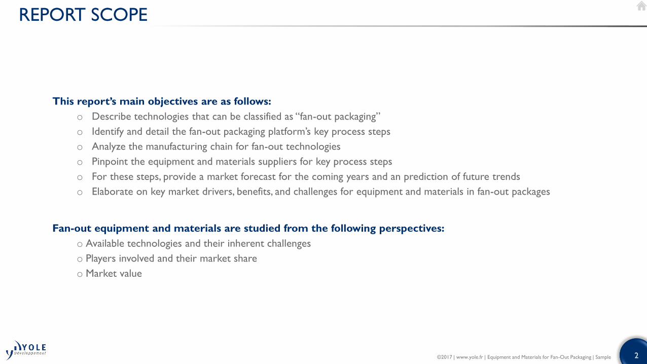
This report’s main objectives are as follows:
o Describe technologies that can be classified as “fan-out packaging”
o Identify and detail the fan-out packaging platform’s key process steps
o Analyze the manufacturing chain for fan-out technologies
o Pinpoint the equipment and materials suppliers for key process steps
o For these steps, provide a market forecast for the coming years and an prediction of future trends
o Elaborate on key market drivers, benefits, and challenges for equipment and materials in fan-out packages
Fan-out equipment and materials are studied from the following perspectives:
o Available technologies and their inherent challenges
o Players involved and their market share
o Market value
©2017 | www.yole.fr | Equipment and Materials for Fan-Out Packaging | Sample
3
REPORT METHODOLOGY
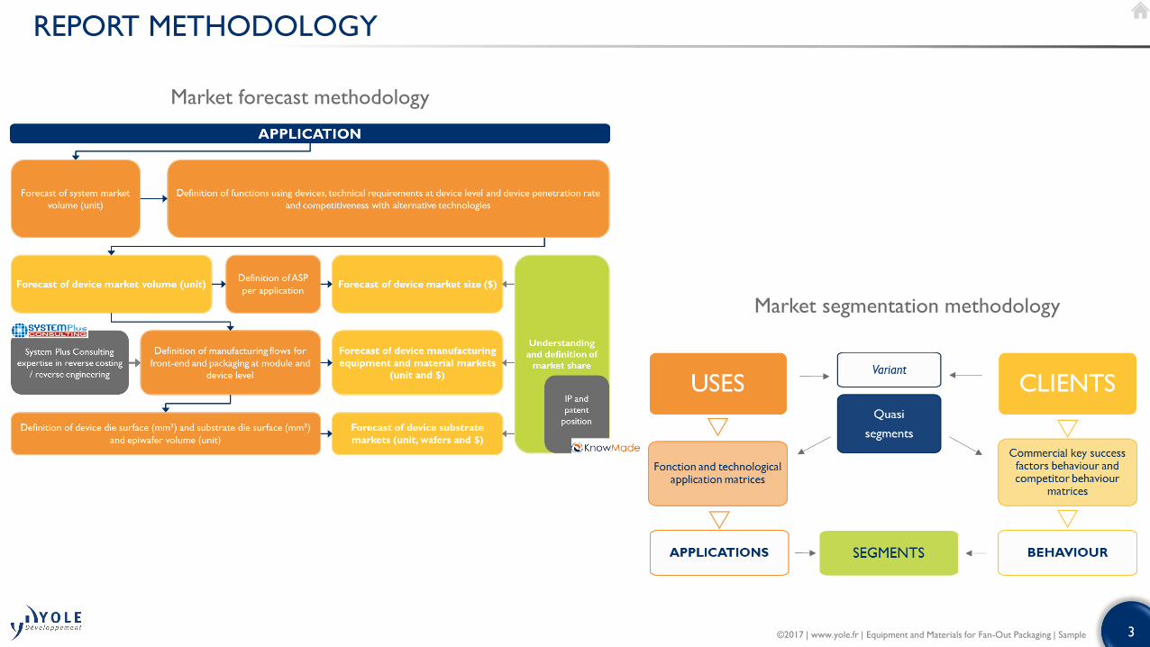
Market segmentation methodology
Market forecast methodology
©2017 | www.yole.fr | Equipment and Materials for Fan-Out Packaging | Sample
4
REPORT METHODOLOGY
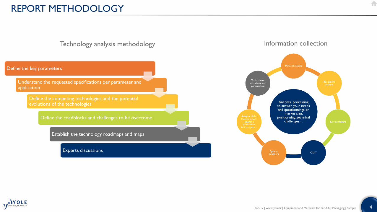
Technology analysis methodology Information collection
©2017 | www.yole.fr | Equipment and Materials for Fan-Out Packaging | Sample
5©2017 | www.yole.fr | Equipment and Materials for Fan-Out Packaging | Sample
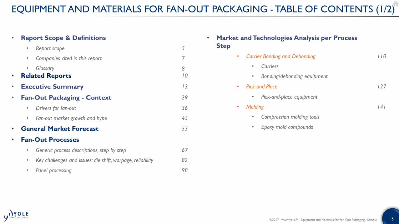
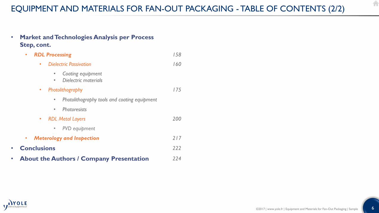
EQUIPMENT AND MATERIALS FOR FAN-OUT PACKAGING - TABLE OF CONTENTS (1/2)
• Market and Technologies Analysis per Process
Step
• Carrier Bonding and Debonding 110
• Carriers
• Bonding/debonding equipment
• Pick-and-Place 127
• Pick-and-place equipment
• Molding 141
• Compression molding tools
• Epoxy mold compounds
• Report Scope & Definitions
• Report scope 5
• Companies cited in this report 7
• Glossary
• Related Reports 8
10
• Executive Summary 13
• Fan-Out Packaging - Context 29
• Drivers for fan-out 36
• Fan-out market growth and hype 45
• General Market Forecast 53
• Fan-Out Processes
• Generic process descriptions, step by step 67
• Key challenges and issues: die shift, warpage, reliability 82
• Panel processing 98
6©2017 | www.yole.fr | Equipment and Materials for Fan-Out Packaging | Sample
EQUIPMENT AND MATERIALS FOR FAN-OUT PACKAGING - TABLE OF CONTENTS (2/2)
• Market and Technologies Analysis per Process
Step, cont.
• RDL Processing 158
• Dielectric Passivation 160
• Coating equipment
• Dielectric materials
• Photolithography 175
• Photolithography tools and coating equipment
• Photoresists
• RDL Metal Layers 200
• PVD equipment
• Meterology and Inspection 217
• Conclusions 222
• About the Authors / Company Presentation 224
Biography & contact
7©2017 | www.yole.fr | Equipment and Materials for Fan-Out Packaging | Sample
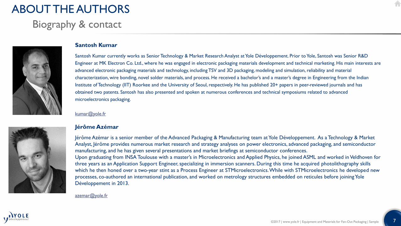
ABOUT THE AUTHORS
Jérôme Azémar
Jérôme Azémar is a senior member of the Advanced Packaging & Manufacturing team at Yole Développement. As a Technology & Market
Analyst, Jérôme provides numerous market research and strategy analyses on power electronics, advanced packaging, and semiconductor
manufacturing, and he has given several presentations and market briefings at semiconductor conferences.
Upon graduating from INSA Toulouse with a master’s in Microelectronics and Applied Physics, he joined ASML and worked in Veldhoven for
three years as an Application Support Engineer, specializing in immersion scanners. During this time he acquired photolithography skills
which he then honed over a two-year stint as a Process Engineer at STMicroelectronics. While with STMicroelectronics he developed new
processes, co-authored an international publication, and worked on metrology structures embedded on reticules before joining Yole
Développement in 2013.
Santosh Kumar
Santosh Kumar currently works as Senior Technology & Market Research Analyst at Yole Développement. Prior to Yole, Santosh was Senior R&D
Engineer at MK Electron Co. Ltd., where he was engaged in electronic packaging materials development and technical marketing. His main interests are
advanced electronic packaging materials and technology, including TSV and 3D packaging, modeling and simulation, reliability and material
characterization, wire bonding, novel solder materials, and process. He received a bachelor’s and a master’s degree in Engineering from the Indian
Institute of Technology (IIT) Roorkee and the University of Seoul, respectively. He has published 20+ papers in peer-reviewed journals and has
obtained two patents. Santosh has also presented and spoken at numerous conferences and technical symposiums related to advanced
microelectronics packaging.

9©2017 | www.yole.fr | Equipment and Materials for Fan-Out Packaging | Sample
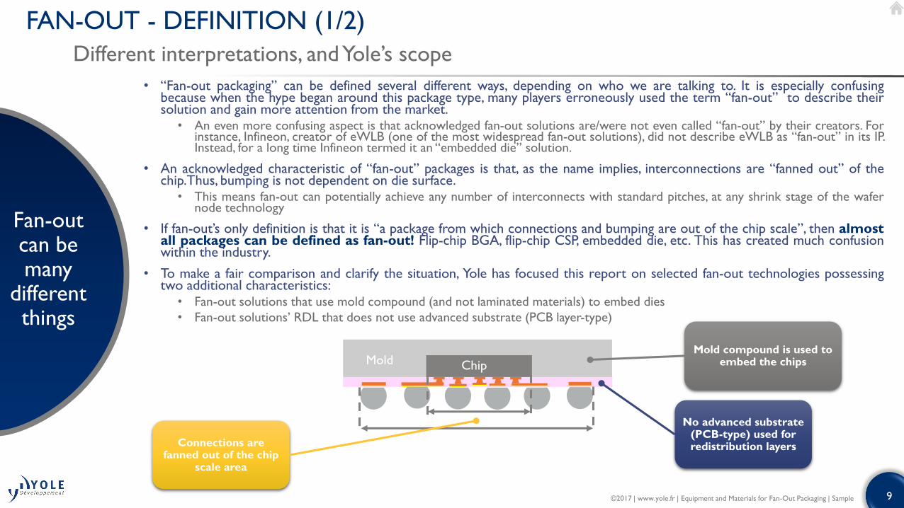
• “Fan-out packaging” can be defined several different ways, depending on who we are talking to. It is especially confusingbecause when the hype began around this package type, many players erroneously used the term “fan-out” to describe theirsolution and gain more attention from the market.
• An even more confusing aspect is that acknowledged fan-out solutions are/were not even called “fan-out” by their creators. Forinstance, Infineon, creator of eWLB (one of the most widespread fan-out solutions), did not describe eWLB as “fan-out” in its IP.Instead, for a long time Infineon termed it an “embedded die” solution.
• An acknowledged characteristic of “fan-out” packages is that, as the name implies, interconnections are “fanned out” of thechip.Thus, bumping is not dependent on die surface.
• This means fan-out can potentially achieve any number of interconnects with standard pitches, at any shrink stage of the wafernode technology
• If fan-out’s only definition is that it is “a package from which connections and bumping are out of the chip scale”, then almostall packages can be defined as fan-out! Flip-chip BGA, flip-chip CSP, embedded die, etc. This has created much confusionwithin the industry.
• To make a fair comparison and clarify the situation, Yole has focused this report on selected fan-out technologies possessingtwo additional characteristics:
• Fan-out solutions that use mold compound (and not laminated materials) to embed dies
• Fan-out solutions’ RDL that does not use advanced substrate (PCB layer-type)
Mold Chip
FAN-OUT - DEFINITION (1/2)
Different interpretations, and Yole’s scope
Fan-out can be many
different things
No advanced substrate (PCB-type) used for redistribution layers
Mold compound is used to embed the chips
Connections are fanned out of the chip
scale area
10©2017 | www.yole.fr | Equipment and Materials for Fan-Out Packaging | Sample
FAN-OUT - DEFINITION (2/2)
What about other technologies called “fan-out”?
Fan-out can be many
different things
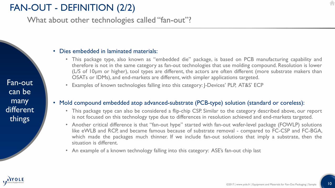
• Dies embedded in laminated materials:
• This package type, also known as “embedded die” package, is based on PCB manufacturing capability andtherefore is not in the same category as fan-out technologies that use molding compound. Resolution is lower(L/S of 10µm or higher), tool types are different, the actors are often different (more substrate makers thanOSATs or IDMs), and end-markets are different, with simpler applications targeted.
• Examples of known technologies falling into this category: J-Devices’ PLP, AT&S’ ECP
• Mold compound embedded atop advanced-substrate (PCB-type) solution (standard or coreless):
• This package type can also be considered a flip-chip CSP. Similar to the category described above, our reportis not focused on this technology type due to differences in resolution achieved and end-markets targeted.
• Another critical difference is that “fan-out hype” started with fan-out wafer-level package (FOWLP) solutionslike eWLB and RCP, and became famous because of substrate removal - compared to FC-CSP and FC-BGA,which made the packages much thinner. If we include fan-out solutions that imply a substrate, then thesituation is different.
• An example of a known technology falling into this category: ASE’s fan-out chip last
11©2017 | www.yole.fr | Equipment and Materials for Fan-Out Packaging | Sample
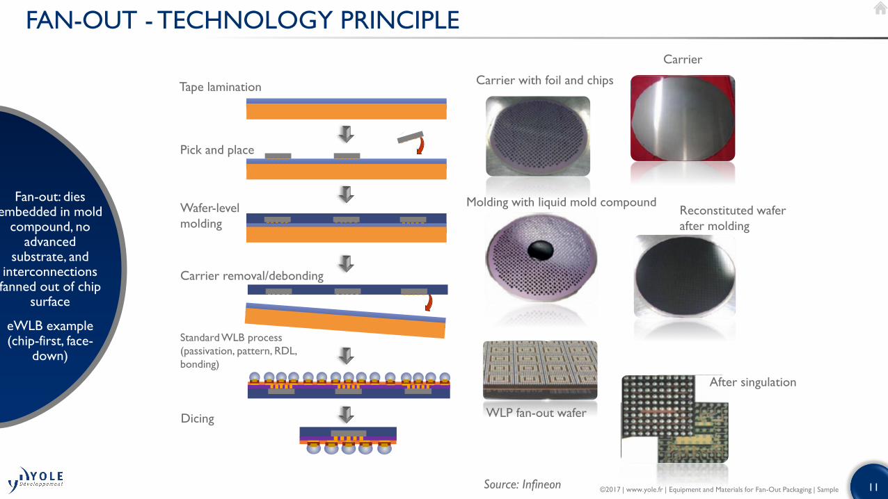
FAN-OUT - TECHNOLOGY PRINCIPLE
Fan-out: dies embedded in mold
compound, no advanced
substrate, and interconnections fanned out of chip
surface
eWLB example (chip-first, face-
down)
Pick and place
Wafer-level
molding
Carrier removal/debonding
Tape lamination
Standard WLB process
(passivation, pattern, RDL,
bonding)
Dicing
Source: Infineon
Carrier
Carrier with foil and chips
Molding with liquid mold compound
WLP fan-out wafer
After singulation
Reconstituted wafer
after molding
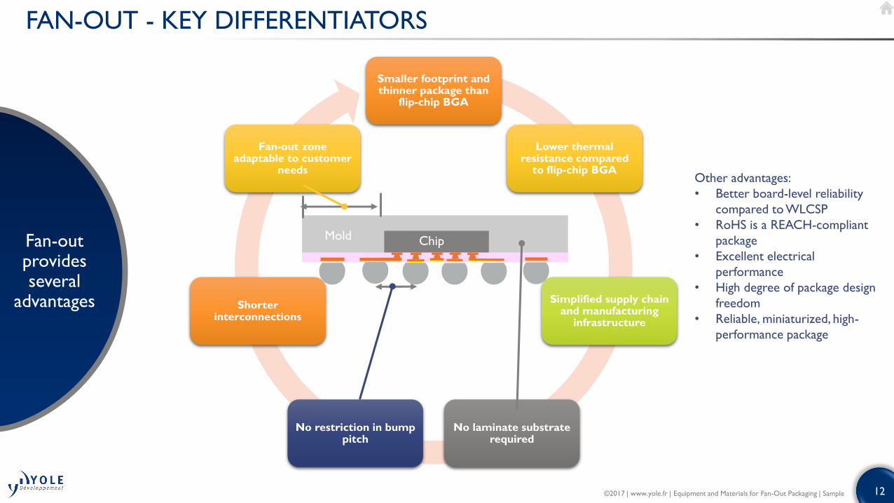
12©2017 | www.yole.fr | Equipment and Materials for Fan-Out Packaging | Sample
Smaller footprint and thinner package than
flip-chip BGA
Lower thermal resistance compared
to flip-chip BGA
Simplified supply chain and manufacturing
infrastructure
No laminate substrate required
No restriction in bump pitch
Shorter interconnections
Fan-out zone adaptable to customer
needs
FAN-OUT - KEY DIFFERENTIATORS
Fan-out provides several
advantages
Mold Chip
Other advantages:
• Better board-level reliability
compared to WLCSP
• RoHS is a REACH-compliant
package
• Excellent electrical
performance
• High degree of package design
freedom
• Reliable, miniaturized, high-
performance package
13©2017 | www.yole.fr | Equipment and Materials for Fan-Out Packaging | Sample
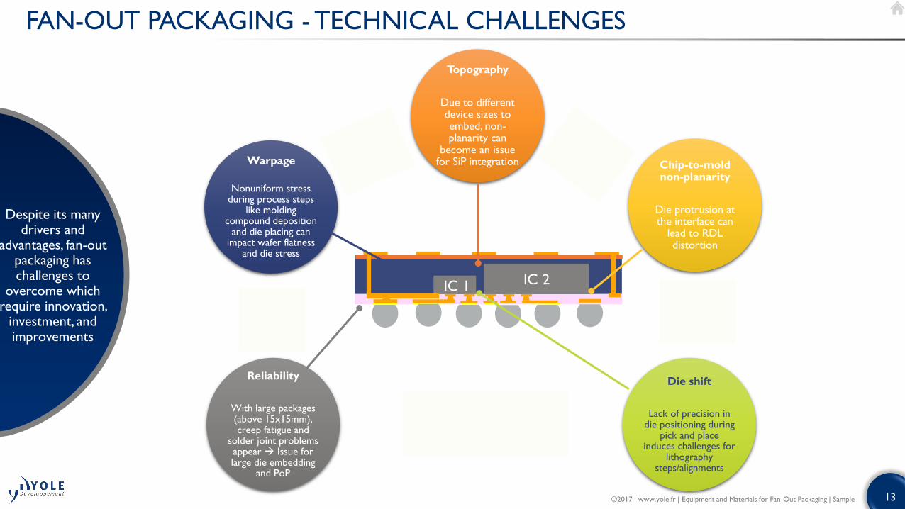
Topography
Due to different device sizes to embed, non-planarity can
become an issue for SiP integration Chip-to-mold
non-planarity
Die protrusion at the interface can
lead to RDL distortion
Die shift
Lack of precision in die positioning during
pick and place induces challenges for
lithography steps/alignments
Reliability
With large packages (above 15x15mm), creep fatigue and
solder joint problemsappear Issue for large die embedding
and PoP
Warpage
Nonuniform stress during process steps
like molding compound deposition
and die placing can impact wafer flatness
and die stress
IC 1 IC 2
FAN-OUT PACKAGING - TECHNICAL CHALLENGES
Despite its manydrivers and
advantages, fan-out packaging has challenges to
overcome whichrequire innovation,
investment, and improvements

14©2017 | www.yole.fr | Equipment and Materials for Fan-Out Packaging | Sample
FAN-OUT ACTIVITY - MARKET FORECAST
Apple’s example will
show competitors
the way
15©2017 | www.yole.fr | Equipment and Materials for Fan-Out Packaging | Sample
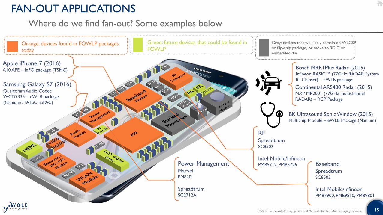
FAN-OUT APPLICATIONS
Where do we find fan-out? Some examples below
Orange: devices found in FOWLP packages
today
Green: future devices that could be found in
FOWLP
Grey: devices that will likely remain on WLCSP
or flip-chip package, or move to 3DIC or
embedded die
Apple iPhone 7 (2016)A10 APE – InFO package (TSMC)
Samsung Galaxy S7 (2016)Qualcomm Audio Codec
WCD9335 – eWLB package
(Nanium/STATSChipPAC)
Bosch MRR1Plus Radar (2015)Infineon RASIC™ (77GHz RADAR System
IC Chipset) – eWLB package
BK Ultrasound Sonic Window (2015)Multichip Module – eWLB Package (Nanium)
BasebandSpreadtrumSC8502
Intel-Mobile/InfineonPMB7900, PMB9810, PMB9801
RFSpreadtrumSC8502
Intel-Mobile/InfineonPMB5712, PMB5726 Power Management
MarvellPM820
SpreadtrumSC2712A
Continental ARS400 Radar (2015)NXP MR2001 (77GHz multichannel
RADAR) – RCP Package
16©2017 | www.yole.fr | Equipment and Materials for Fan-Out Packaging | Sample
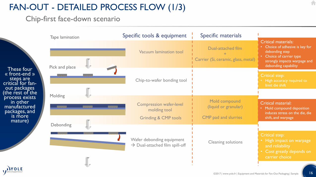
FAN-OUT - DETAILED PROCESS FLOW (1/3)
Chip-first face-down scenario
These four « front-end »
steps are critical for fan-out packages
(the rest of the process exists
in other manufactured packages, and
is more mature)
Specific tools & equipment Specific materials
Chip-to-wafer bonding tool
Wafer debonding equipment
Dual-attached film spill-off
Mold compound
(liquid or granular)
Dual-attached film
+
Carrier (Si, ceramic, glass, metal)
Compression wafer-level
molding tool
Vacuum lamination tool
Cleaning solutions
Grinding & CMP tools CMP pad and slurries
Tape lamination
Pick and place
Molding
Debonding
Critical materials: • Choice of adhesive is key for
debonding step
• Choice of carrier type
strongly impacts warpage and
debonding capability
Critical material: • Mold compound deposition
induces stress on the die, die
shift, and warpage
Critical step: • High accuracy required to
limit die shift
Critical step:
• High impact on warpage
and reliability
• Cost greatly depends on
carrier choice
17©2017 | www.yole.fr | Equipment and Materials for Fan-Out Packaging | Sample
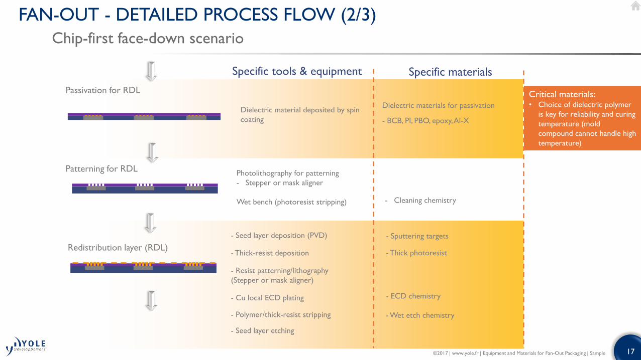
Passivation for RDL
Redistribution layer (RDL)
Patterning for RDLPhotolithography for patterning
- Stepper or mask aligner
Wet bench (photoresist stripping)
- Seed layer deposition (PVD)
- Thick-resist deposition
- Resist patterning/lithography
(Stepper or mask aligner)
- Cu local ECD plating
- Polymer/thick-resist stripping
- Seed layer etching
- Sputtering targets
- Thick photoresist
- ECD chemistry
- Wet etch chemistry
- Cleaning chemistry
Dielectric material deposited by spin
coating
Dielectric materials for passivation
- BCB, PI, PBO, epoxy, Al-X
FAN-OUT - DETAILED PROCESS FLOW (2/3)
Chip-first face-down scenario
Specific materials
Critical materials: • Choice of dielectric polymer
is key for reliability and curing
temperature (mold
compound cannot handle high
temperature)
Specific tools & equipment
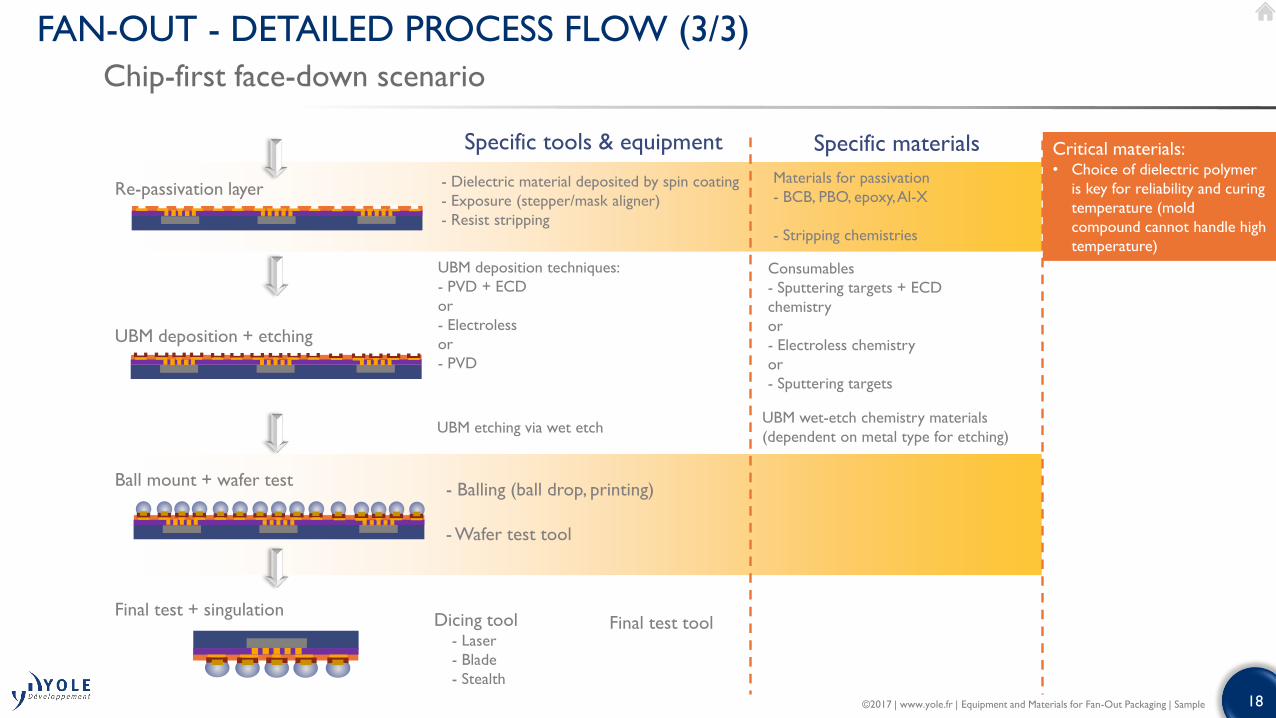
18©2017 | www.yole.fr | Equipment and Materials for Fan-Out Packaging | Sample
UBM etching via wet etch
Final test + singulation
Ball mount + wafer test
Re-passivation layer
UBM deposition + etching
Dicing tool- Laser
- Blade
- Stealth
- Dielectric material deposited by spin coating
- Exposure (stepper/mask aligner)
- Resist stripping
Materials for passivation
- BCB, PBO, epoxy, Al-X
- Stripping chemistries
UBM deposition techniques:
- PVD + ECD
or
- Electroless
or
- PVD
Consumables
- Sputtering targets + ECD
chemistry
or
- Electroless chemistry
or
- Sputtering targets
UBM wet-etch chemistry materials
(dependent on metal type for etching)
Final test tool
FAN-OUT - DETAILED PROCESS FLOW (3/3)
Chip-first face-down scenario
- Balling (ball drop, printing)
- Wafer test tool
Critical materials: • Choice of dielectric polymer
is key for reliability and curing
temperature (mold
compound cannot handle high
temperature)
Specific materialsSpecific tools & equipment
19©2017 | www.yole.fr | Equipment and Materials for Fan-Out Packaging | Sample
FAN-OUT PROCESS STEPS TO FOCUS ON (1/2)
• In this report, Yole focuses on some specific process steps. These steps are considered more specific and illustrative offan-out packaging, as well as areas showing strong innovation from different players:
• Pick and place:
• Pick-and-place is a key step for FOWLP. The process speed directly impacts the production pace, and die positioning accuracy hasconsequences on RDL manufacturing.
• Bonding/debonding:
• A trademark step of fan-out packaging is the bonding of chips on carriers’ surface and debonding them once the reconstituted wafer ismolded. This step directly impacts package reliability and defines this platform’s feasibility. It impacts warpage, defectiveness, and packagemanufacturing success.
• Mold compound deposition:
• Mold deposition is fan-out packaging’s most illustrative step. Mold constitutes the package itself, and embeds the chips. Creating areconstituted wafer/panel and processing it is at the very core of fan-out manufacturing.
• RDL process:
• Redistribution layers are the source of the “fan-out” packaging name. They allow the connections to transcend the chip surface and not belimited by it. All steps are essential: polymers’ passivation coating, patterning them thanks to photolithography, and creating copperconnection layers through plating (after first sputtering the seed).This process impacts package thickness and efficiency
• Metrology:
• Metrology steps are very important for guaranteeing good process execution. In the case of fan-out, some steps that are not commonlymeasured in advanced packaging (i.e. warpage) become mandatory to follow.
20©2017 | www.yole.fr | Equipment and Materials for Fan-Out Packaging | Sample
FAN-OUT PROCESS STEPS TO FOCUS ON (2/2)
• What about other process steps?
• All manufacturing steps are important for an optimum process, but some steps were not considered during our investigation.Several reasons for this: either we did not have enough information on these steps, or they were closed markets, or we deemedthem less characteristic of FOWLP. For relevance and information quantity’s sake, Yole has focused its investigation on theprocess steps listed on the previous slide. However, we are capable of studying other steps and their associated equipment andmaterials upon request, if desired.
• List of steps not investigated in this report:
• UBM deposition and etching
• Ball mounting
• Wafer testing
• Dicing
• Some steps were investigated only at a technical level, and a market study was not performed:
• Carriers (market forecasts available only for glass carriers)
• Metrology steps
21©2017 | www.yole.fr | Equipment and Materials for Fan-Out Packaging | Sample
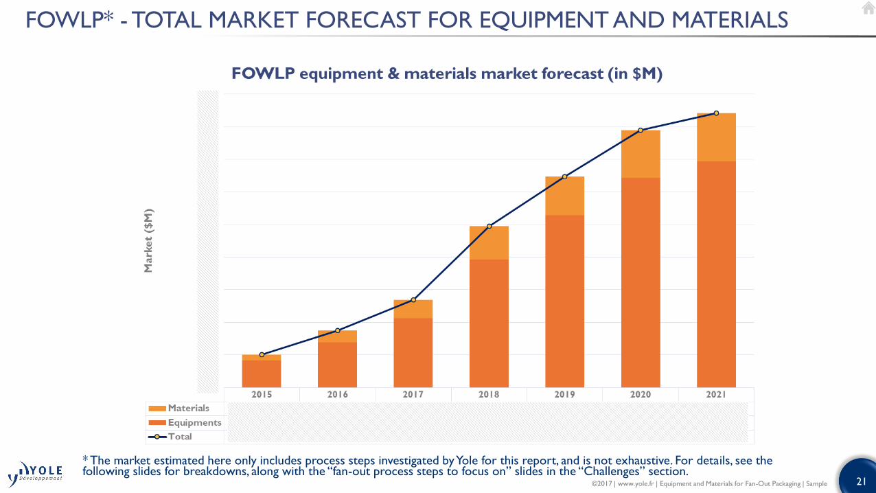
FOWLP* - TOTAL MARKET FORECAST FOR EQUIPMENT AND MATERIALS
* The market estimated here only includes process steps investigated by Yole for this report, and is not exhaustive. For details, see the following slides for breakdowns, along with the “fan-out process steps to focus on” slides in the “Challenges” section.
22©2017 | www.yole.fr | Equipment and Materials for Fan-Out Packaging | Sample
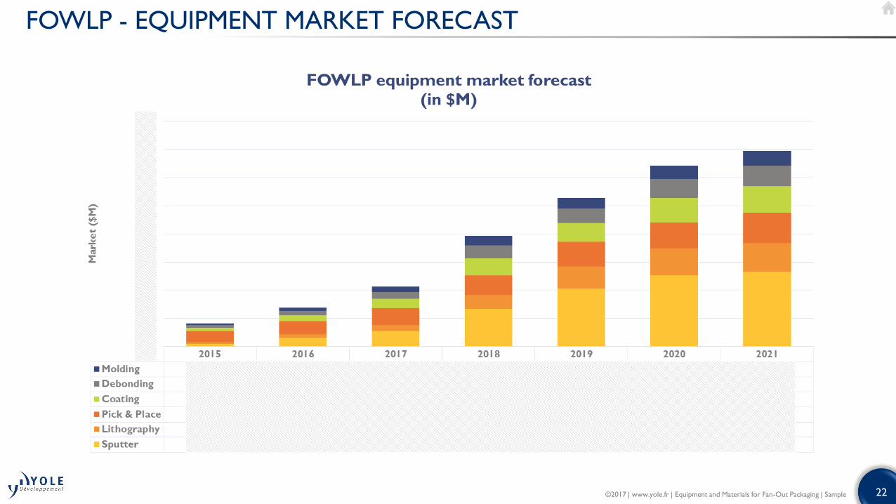
FOWLP - EQUIPMENT MARKET FORECAST
23©2017 | www.yole.fr | Equipment and Materials for Fan-Out Packaging | Sample
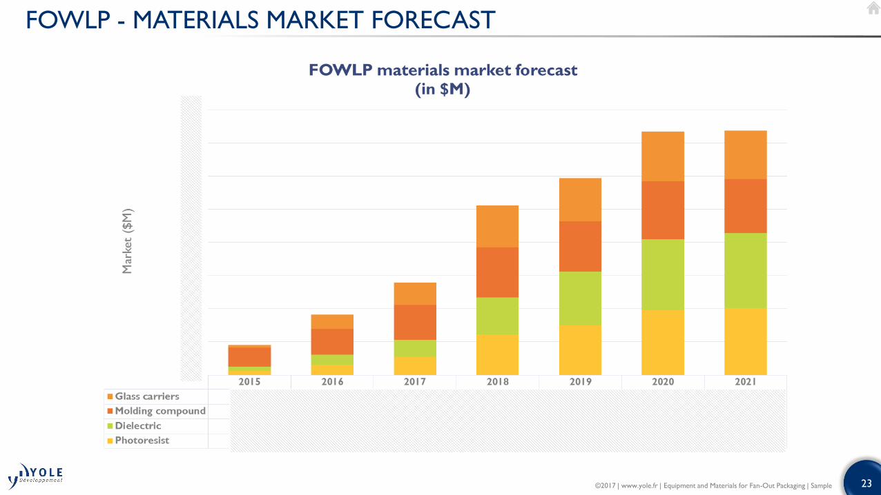
FOWLP - MATERIALS MARKET FORECAST
24©2017 | www.yole.fr | Equipment and Materials for Fan-Out Packaging | Sample
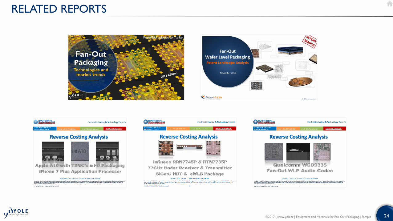
RELATED REPORTS

ORDER FORMEquipment & Materials for Fan-Out Packaging 2017
SHIPPING CONTACT
First Name:
Email:
Last Name:
Phone:
PAYMENT
BY CREDIT CARD Visa Mastercard Amex
Name of the Card Holder:
Credit Card Number:
Card Verification Value (3 digits except AMEX: 4 digits):
Expiration date:
BY BANK TRANSFERBANK INFO: HSBC, 1 place de la Bourse, F-69002 Lyon, France, Bank code: 30056, Branch code: 00170Account No: 0170 200 1565 87, SWIFT or BIC code: CCFRFRPP, IBAN: FR76 3005 6001 7001 7020 0156 587
RETURN ORDER BY • FAX: +33 (0)472 83 01 83• MAIL: YOLE DÉVELOPPEMENT, Le Quartz,
75 Cours Emile Zola, 69100 Villeurbanne/Lyon - France
SALES CONTACTS • North America - Steve Laferriere: +13106 008 267
[email protected] • Europe & RoW - Lizzie Levenez: + 49 15 123 544 182
[email protected]• Japan & Rest of Asia - Takashi Onozawa: +81 3 6869 6970
[email protected] • Greater China - Mavis Wang: +886 979 336 809
[email protected]• Specific inquiries: +33 472 830 180 – [email protected]
(1) Our Terms and Conditions of Sale are available at www.yole.fr/Terms_and_Conditions_of_Sale.aspx The present document is valid 24 months after its publishing date: March 28, 2017
/
ABOUT YOLE DEVELOPPEMENT
BILL TO
Name (Mr/Ms/Dr/Pr):
Job Title:
Company:
Address:
City:
State:
Postcode/Zip:
Country*:
*VAT ID Number for EU members:
Tel:
Email:
Date:
PRODUCT ORDER - Ref YDAP17011Please enter my order for above named report: One user license*: Euro 5,490 Multi user license: Euro 6,490- The report will be ready for delivery from March 28, 2017- For price in dollars, please use the day’s exchange rate. All reports are
delivered electronically at payment reception. For French customers, add 20% for VAT
I hereby accept Yole Développement’s Terms and Conditions of Sale(1)
Signature:
*One user license means only one person at the company can use the report.
Founded in 1998, Yole Développement has grown to become a group of companies providing marketing, technology and strategy consulting, media and corporate finance services. With a strong focus on emerging applications using silicon and/or micro manufacturing, the Yole Développement group has expanded to include more than 50 collaborators worldwide covering MEMS, Compound Semiconductors, LED, Displays, Image Sensors, Optoelectronics, Microfluidics & Medical, Advanced Packaging, Manufacturing, Nanomaterials, Power Electronics and Batteries & Energy Management.The “More than Moore” company Yole and its partners System Plus Consulting, Blumorpho, KnowMade and PISEO support industrial companies, investors and R&D organizations worldwide to help them understand markets and follow technology trends to develop their business.
MEDIA & EVENTS• i-Micronews.com, online disruptive technologies website• @Micronews, weekly e-newsletter• Communication & webcasts services• Events: Yole Seminars, Market Briefings…More information on www.i-micronews.com
CONTACTSFor more information about :• Consulting Services: Jean-Christophe Eloy ([email protected])• Financial Services: Jean-Christophe Eloy ([email protected])• Report Business: Fayçal Khamassi ([email protected])• Press relations: Sandrine Leroy ([email protected])
CONSULTING• Market data & research, marketing analysis• Technology analysis• Reverse engineering & costing services• Strategy consulting• Patent analysisMore information on www.yole.fr
REPORTS• Collection of technology & market reports• Manufacturing cost simulation tools• Component reverse engineering & costing
analysis• Patent investigationMore information on www.i-micronews.com/reports
FINANCIAL SERVICES• Mergers & Acquisitions• Due diligence• FundraisingMore information on Jean-Christophe Eloy ([email protected])

© 2017
From Technologies to Market
Yole Développement
FromTechnologies to Market
26©2017 | www.yole.fr | Equipment and Materials for Fan-Out Packaging | Sample
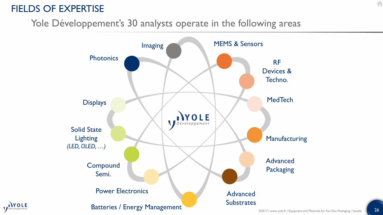
FIELDS OF EXPERTISE
Yole Développement’s 30 analysts operate in the following areas
MEMS & Sensors
Compound
Semi.
Imaging
Photonics
MedTech
Manufacturing
Advanced
Packaging
Batteries / Energy Management
Power Electronics
Displays
RF
Devices &
Techno.
Advanced
Substrates
Solid State
Lighting(LED, OLED, …)

27©2017 | www.yole.fr | Equipment and Materials for Fan-Out Packaging | Sample
4 BUSINESS MODELS
o Consulting and Analysis
• Market data & research, marketing analysis
• Technology analysis
• Strategy consulting
• Reverse engineering & costing
• Patent analysis
www.yole.fr
o Reports
• Market & technology reports
• Patent Investigation and patent infringement risk analysis
• Teardowns & reverse costing analysis
• Cost simulation tool
www.i-Micronews.com/reports
o Financial services
• M&A (buying and selling)
• Due diligence
• Fundraising
• Maturation of companies
• IP portfolio management & optimization
www.yolefinance.com
www.bmorpho.com
o Media
• i-Micronews.com website
• @Micronews e-newsletter
• Communication & webcast services
• Events
www.i-Micronews.com
28©2017 | www.yole.fr | Equipment and Materials for Fan-Out Packaging | Sample
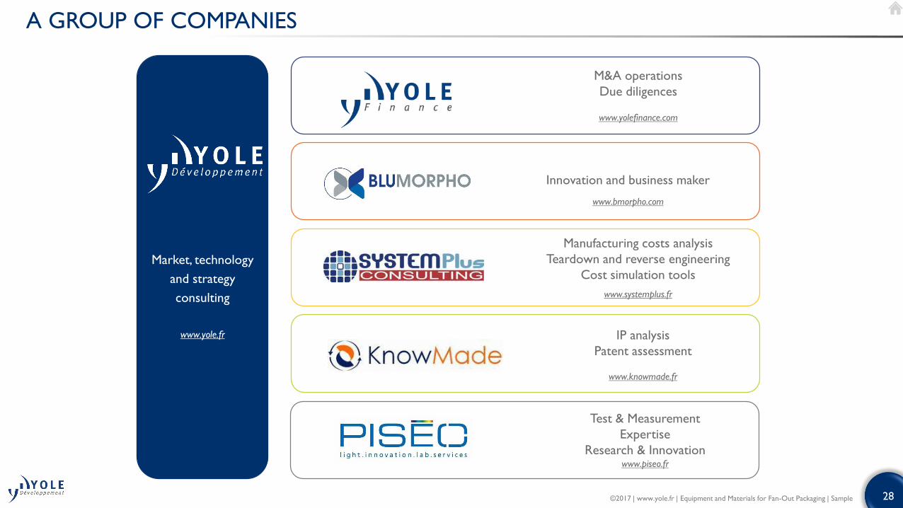
A GROUP OF COMPANIES
Market, technology
and strategy
consulting
www.yole.fr
M&A operations
Due diligences
www.yolefinance.com
Manufacturing costs analysis
Teardown and reverse engineering
Cost simulation tools
www.systemplus.fr
IP analysis
Patent assessment
www.knowmade.fr
Innovation and business maker
www.bmorpho.com
Test & Measurement
Expertise
Research & Innovationwww.piseo.fr

29©2017 | www.yole.fr | Equipment and Materials for Fan-Out Packaging | Sample
OUR GLOBAL ACTIVITY
30%of our business
40%of our business 30%
of our business
Yole Inc.
Greater
China office
Yole Japan
HQ in Lyon
Nantes
Paris
Nice
Vénissieux
Europe office
Frankfurt
Hsinchu
Tokyo
Phoenix
Yole Korea
Seoul

30©2017 | www.yole.fr | Equipment and Materials for Fan-Out Packaging | Sample
RESEARCH PRODUCTS - CONTENT COMPARISON
Custom analysis scope is defined with
you to meet your information and
budget needs
Breadth of the analysis
Dep
th o
f th
e a
naly
sis
Custom
Analysis
Workshops
Standard Reports
31©2017 | www.yole.fr | Equipment and Materials for Fan-Out Packaging | Sample
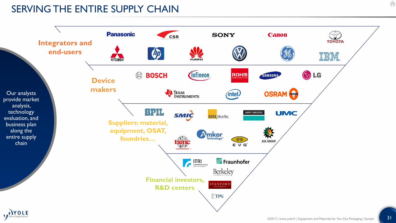
SERVING THE ENTIRE SUPPLY CHAIN
Our analysts provide market
analysis, technology
evaluation, and business plan
along the entire supply
chain
Integrators and
end-users
Device
makers
Suppliers: material,
equipment, OSAT,
foundries…
Financial investors,
R&D centers
32©2017 | www.yole.fr | Equipment and Materials for Fan-Out Packaging | Sample
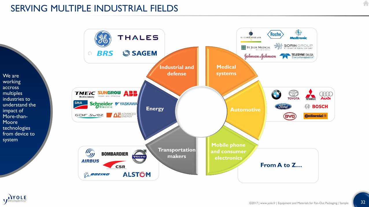
SERVING MULTIPLE INDUSTRIAL FIELDS
We are workingaccrossmultiples industries to understand the impact of More-than-Moore technologies from device to system
From A to Z…
Transportation
makers
Mobile phone
and consumer
electronics
Automotive
Medical
systemsIndustrial and
defense
Energy
33©2017 | www.yole.fr | Equipment and Materials for Fan-Out Packaging | Sample
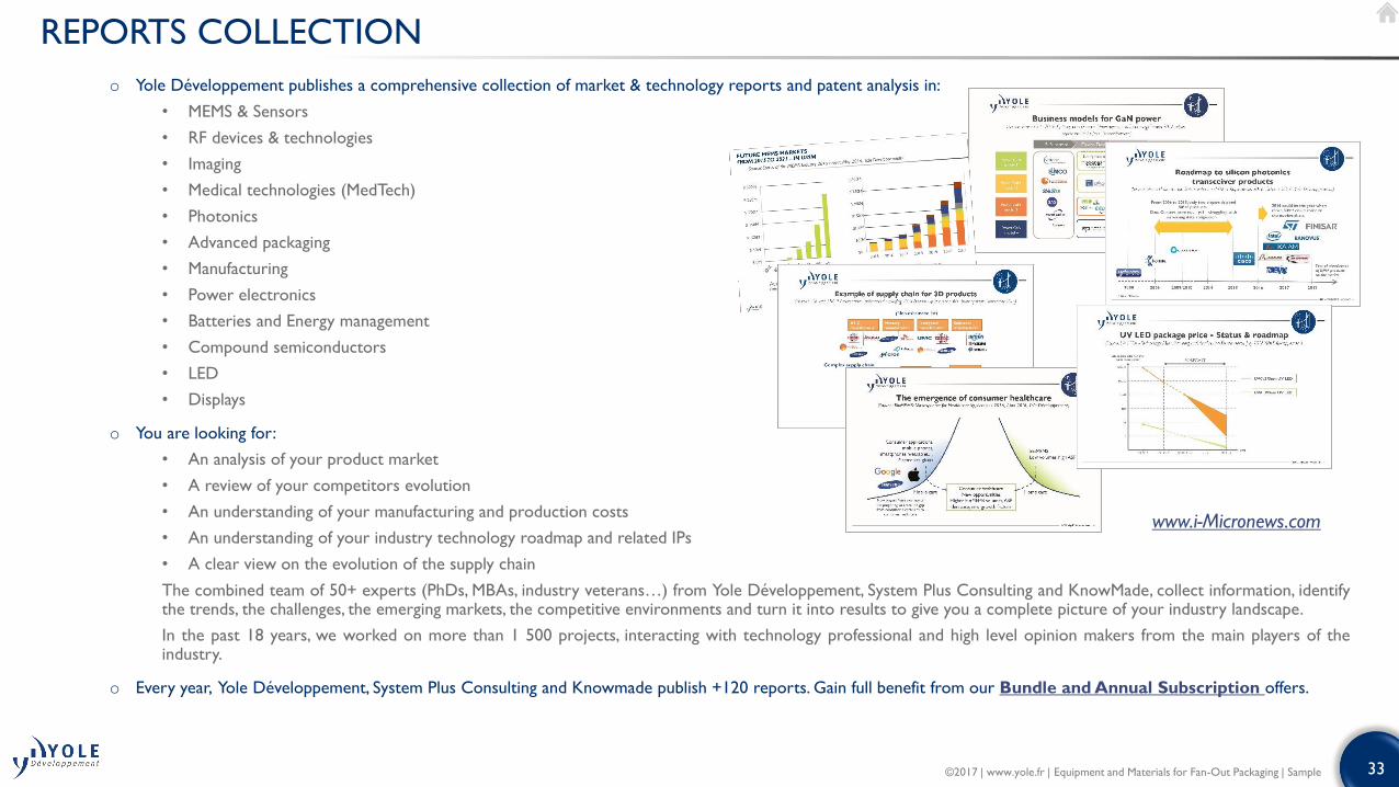
REPORTS COLLECTION
o Yole Développement publishes a comprehensive collection of market & technology reports and patent analysis in:
• MEMS & Sensors
• RF devices & technologies
• Imaging
• Medical technologies (MedTech)
• Photonics
• Advanced packaging
• Manufacturing
• Power electronics
• Batteries and Energy management
• Compound semiconductors
• LED
• Displays
o You are looking for:
• An analysis of your product market
• A review of your competitors evolution
• An understanding of your manufacturing and production costs
• An understanding of your industry technology roadmap and related IPs
• A clear view on the evolution of the supply chain
The combined team of 50+ experts (PhDs, MBAs, industry veterans…) from Yole Développement, System Plus Consulting and KnowMade, collect information, identifythe trends, the challenges, the emerging markets, the competitive environments and turn it into results to give you a complete picture of your industry landscape.
In the past 18 years, we worked on more than 1 500 projects, interacting with technology professional and high level opinion makers from the main players of theindustry.
o Every year, Yole Développement, System Plus Consulting and Knowmade publish +120 reports. Gain full benefit from our Bundle and Annual Subscription offers.
www.i-Micronews.com
34©2017 | www.yole.fr | Equipment and Materials for Fan-Out Packaging | Sample
OUR 2017 REPORTS PLANNING (1/2)
MARKET AND TECHNOLOGY REPORTS by Yole Développement
o MEMS & SENSORS
− Fingerprint Sensor Applications and Technologies - Consumer Market Focus 2017
− MEMS Microphones, Speakers and Audio Solutions 2017
− Status of the MEMS Industry 2017
− MEMS & Sensors for Automotive 2017
− High End Inertial Sensors for Defense and Industrial Applications 2017
− Sensor Modules for Smart Building 2017
− Sensing and Display for AR/VR/MR 2017 (Vol 1)
− MEMS Packaging 2017
− Magnetic Sensors Market and Technologies 2017**
− Microspectrometers Markets and Applications 2017**
o RF DEVICES AND TECHNOLOGIES
− RF Components and Modules for Cellphones 2017
− Advanced RF SiP for Cellphones 2017
− 5G and Beyond (Vol 1): Impact on RF Industry, from Infrastructure to Terminals
2017
− 5G and Beyond (Vol 2): RF Materials Platform, from Infrastructure to Terminals
2017
− RF Technologies for Automotive Applications 2017
− GaN and Si LDMOS Market and Technology Trends for RF Power 2017
o IMAGING & OPTOELECTRONICS
− 3D Imaging & Sensing 2017
− Status of the CMOS Image Sensor Industry 2017
− Camera Module for Consumer and Automotive Applications 2017
− Uncooled Infrared Imaging Technology & Market Trends 2017
− Active Imaging and Lidars 2017 (vol 1)
o MEDTECH
− Status of the Microfluidics Industry 2017
− Solid State Medical Imaging 2017
− Sensors for HomeCare 2017
− Sensors for Medical Robotics 2017
− Organs-on-a Chip 2017
o ADVANCED PACKAGING
− Advanced Substrates Overview 2017
− Status of the Advanced Packaging Industry 2017
− Fan Out Packaging: Market & Technology Trends 2017
− 3D Business Update: Market & Technology Trends 2017
− Advanced QFN: Market & Technology Trends 2017**
− Inspection and Metrology for Advanced Packaging Platform 2017**
− Advanced Packaging for Memories 2017
− Embedded Die Packaging: Technologies and Markets Trends 2017
o MANUFACTURING
− Glass Substrate Manufacturing 2017
− Equipment & Materials for Fan Out Technology 2017
− Equipment & Materials for 3D T(X)V Technology 2017
− Emerging Non Volatile Memories 2017
** To be confirmed
35©2017 | www.yole.fr | Equipment and Materials for Fan-Out Packaging | Sample
OUR 2017 REPORTS PLANNING (2/2)
o POWER ELECTRONICS
− Status of Power Electronics Industry 2017
− Power Mosfets Market and Technology Trends 2017
− IGBT Market and Technology Trends 2017
− Power Packaging Market and Technology Trends 2017
− Power SiC 2017: Materials, Devices, and Applications
− Power GaN 2017: Materials, Devices, and Applications
− Materials Market Opportunities for Cellphone Thermal Management (Battery
Cooling, Fast Charging, Data Processing, Battery Cooling, etc.) 2017
− Gate Driver Market and Technology Trends in Power Electronics 2017
− Power Management ICs Market Quarterly Update 2017
− Power Electronics for Electrical Aircraft, Rail and Buses 2017
− Thermal Management for LED and Power 2017
o BATTERY AND ENERGY MANAGEMENT
− Status of Battery Industry for Stationary, Automotive and Consumer Applications
2017
o COMPOUND SEMICONDUCTORS
− Power SiC 2017: Materials, Devices, and Applications
− Power GaN 2017: Materials, Devices, and Applications
− GaN and Si LDMOS Market and Technology Trends for RF Power 2017
− Bulk GaN Technology Status and Market Expectations (Power, LED, Lasers) 2017
o DISPLAYS
− Microdisplays and MicroLEDs 2017
− Display for Augmented Reality, Virtual Reality and Mixed Reality 2017
− QD for Display Applications 2017
− Phosphors & Quantum Dots 2017 - LED Downconverters for Lighting & Displays
− Emerging Display Technologies 2017**
o LED
− UV LEDs 2017 - Technology, Manufacturing and Application Trends
− Agricultural Lighting 2017 - Technology, Industry and Market Trends
− Automotive Lighting 2017 - Technology, Industry and Market Trends
− Active Imaging and Lidar 2017 (Vol 2) - IR Lighting**
− LED Lighting Module 2017 - Technology, Industry and Market Trends
− IR LEDs 2017 - Technology, Manufacturing and Application Trends
− Phosphors & Quantum Dots 2017 - LED Downconverters for Lighting & Displays
− CSP LED Module 2017
− LED Packaging 2017
PATENT ANALYSIS by Knowmade
− 3D Monolithic Memory: Patent Landscape Analysis
− Microfluidic Diagnostic: Patent Landscape Analysis
− GaN Technology: Top-100 IP profiles**
− Uncooled Infrared Imaging: Patent Landscape Analysis**
− MEMS Microphone: Patent Landscape Analysis**
− MEMS Microphone: Knowles' Patent Portfolio Analysis**
− MicroLEDs: Patent Landscape Analysis**
− Microbolometer: Patents used in products**
− Micropumps: Patent Landscape Analysis**
− Flexible batteries: Patent Landscape Analysis**
TEARDOWN & REVERSE COSTING by System Plus Consulting More than 60 teardowns and reverse costing analysis and cost simulation tools to be
published in 2017.
** To be confirmed
36©2017 | www.yole.fr | Equipment and Materials for Fan-Out Packaging | Sample
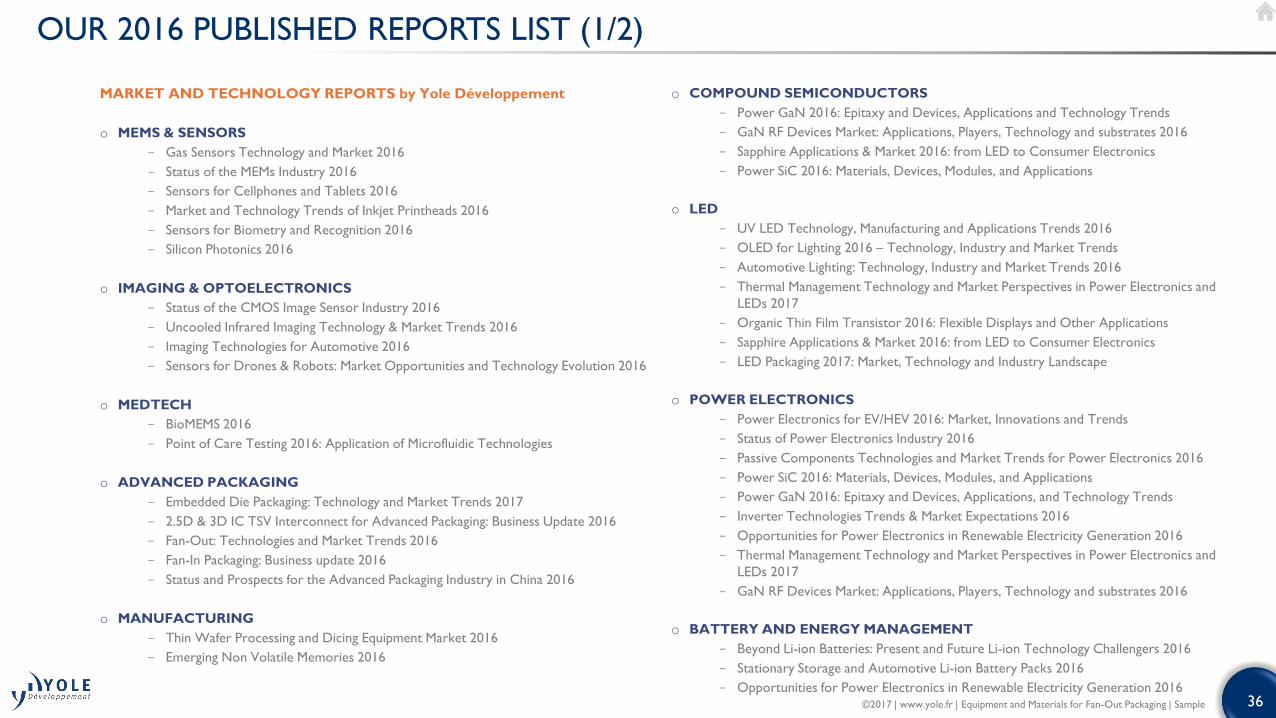
OUR 2016 PUBLISHED REPORTS LIST (1/2)
MARKET AND TECHNOLOGY REPORTS by Yole Développement
o MEMS & SENSORS
− Gas Sensors Technology and Market 2016
− Status of the MEMs Industry 2016
− Sensors for Cellphones and Tablets 2016
− Market and Technology Trends of Inkjet Printheads 2016
− Sensors for Biometry and Recognition 2016
− Silicon Photonics 2016
o IMAGING & OPTOELECTRONICS
− Status of the CMOS Image Sensor Industry 2016
− Uncooled Infrared Imaging Technology & Market Trends 2016
− Imaging Technologies for Automotive 2016
− Sensors for Drones & Robots: Market Opportunities and Technology Evolution 2016
o MEDTECH
− BioMEMS 2016
− Point of Care Testing 2016: Application of Microfluidic Technologies
o ADVANCED PACKAGING
− Embedded Die Packaging: Technology and Market Trends 2017
− 2.5D & 3D IC TSV Interconnect for Advanced Packaging: Business Update 2016
− Fan-Out: Technologies and Market Trends 2016
− Fan-In Packaging: Business update 2016
− Status and Prospects for the Advanced Packaging Industry in China 2016
o MANUFACTURING
− Thin Wafer Processing and Dicing Equipment Market 2016
− Emerging Non Volatile Memories 2016
o COMPOUND SEMICONDUCTORS
− Power GaN 2016: Epitaxy and Devices, Applications and Technology Trends
− GaN RF Devices Market: Applications, Players, Technology and substrates 2016
− Sapphire Applications & Market 2016: from LED to Consumer Electronics
− Power SiC 2016: Materials, Devices, Modules, and Applications
o LED
− UV LED Technology, Manufacturing and Applications Trends 2016
− OLED for Lighting 2016 – Technology, Industry and Market Trends
− Automotive Lighting: Technology, Industry and Market Trends 2016
− Thermal Management Technology and Market Perspectives in Power Electronics and
LEDs 2017
− Organic Thin Film Transistor 2016: Flexible Displays and Other Applications
− Sapphire Applications & Market 2016: from LED to Consumer Electronics
− LED Packaging 2017: Market, Technology and Industry Landscape
o POWER ELECTRONICS
− Power Electronics for EV/HEV 2016: Market, Innovations and Trends
− Status of Power Electronics Industry 2016
− Passive Components Technologies and Market Trends for Power Electronics 2016
− Power SiC 2016: Materials, Devices, Modules, and Applications
− Power GaN 2016: Epitaxy and Devices, Applications, and Technology Trends
− Inverter Technologies Trends & Market Expectations 2016
− Opportunities for Power Electronics in Renewable Electricity Generation 2016
− Thermal Management Technology and Market Perspectives in Power Electronics and
LEDs 2017
− GaN RF Devices Market: Applications, Players, Technology and substrates 2016
o BATTERY AND ENERGY MANAGEMENT
− Beyond Li-ion Batteries: Present and Future Li-ion Technology Challengers 2016
− Stationary Storage and Automotive Li-ion Battery Packs 2016
− Opportunities for Power Electronics in Renewable Electricity Generation 2016
37©2017 | www.yole.fr | Equipment and Materials for Fan-Out Packaging | Sample
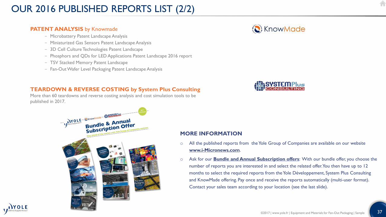
OUR 2016 PUBLISHED REPORTS LIST (2/2)
PATENT ANALYSIS by Knowmade
− Microbattery Patent Landscape Analysis
− Miniaturized Gas Sensors Patent Landscape Analysis
− 3D Cell Culture Technologies Patent Landscape
− Phosphors and QDs for LED Applications Patent Landscape 2016 report
− TSV Stacked Memory Patent Landscape
− Fan-Out Wafer Level Packaging Patent Landscape Analysis
TEARDOWN & REVERSE COSTING by System Plus Consulting More than 60 teardowns and reverse costing analysis and cost simulation tools to be
published in 2017.
MORE INFORMATION
o All the published reports from the Yole Group of Companies are available on our website
www.i-Micronews.com.
o Ask for our Bundle and Annual Subscription offers: With our bundle offer, you choose the
number of reports you are interested in and select the related offer. You then have up to 12
months to select the required reports from the Yole Développement, System Plus Consulting
and KnowMade offering. Pay once and receive the reports automatically (multi-user format).
Contact your sales team according to your location (see the last slide).
38©2017 | www.yole.fr | Equipment and Materials for Fan-Out Packaging | Sample
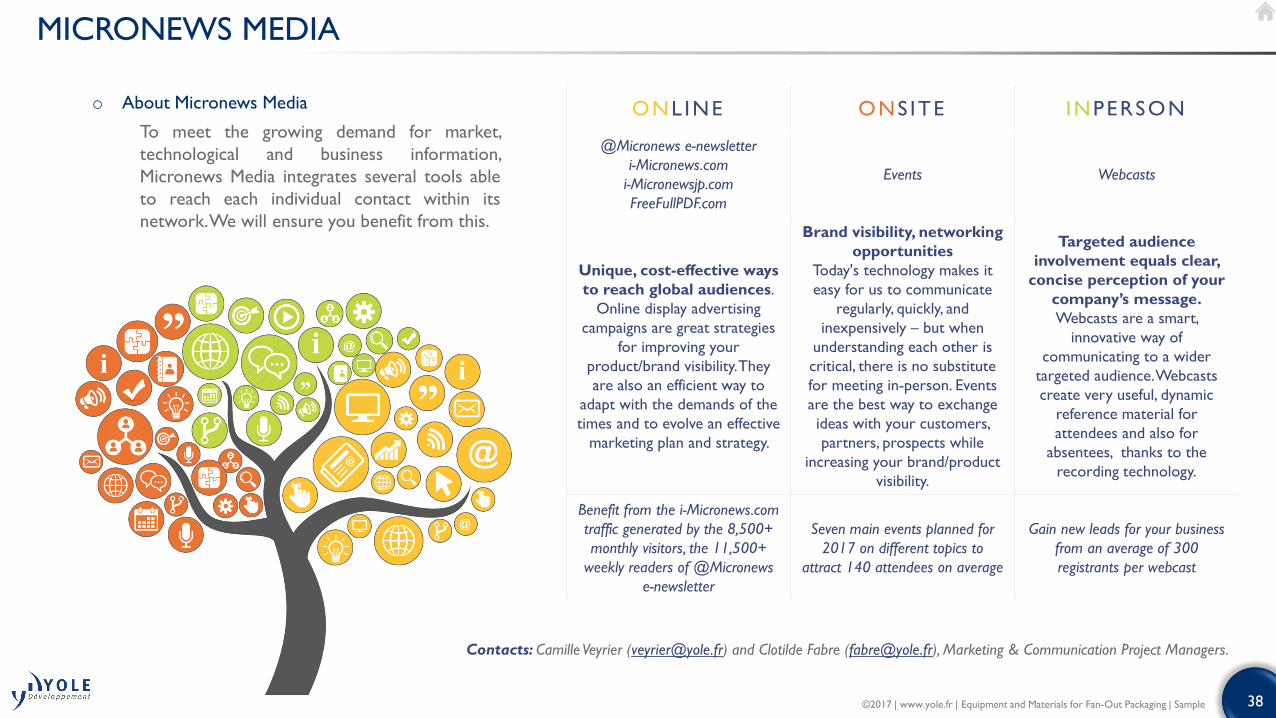
MICRONEWS MEDIA
o About Micronews Media
To meet the growing demand for market,
technological and business information,
Micronews Media integrates several tools able
to reach each individual contact within its
network.We will ensure you benefit from this.
ONLINE ONSITE INPERSON
@Micronews e-newsletter
i-Micronews.com
i-Micronewsjp.com
FreeFullPDF.com
Events Webcasts
Unique, cost-effective ways
to reach global audiences.
Online display advertising
campaigns are great strategies
for improving your
product/brand visibility. They
are also an efficient way to
adapt with the demands of the
times and to evolve an effective
marketing plan and strategy.
Brand visibility, networking
opportunities
Today's technology makes it
easy for us to communicate
regularly, quickly, and
inexpensively – but when
understanding each other is
critical, there is no substitute
for meeting in-person. Events
are the best way to exchange
ideas with your customers,
partners, prospects while
increasing your brand/product
visibility.
Targeted audience
involvement equals clear,
concise perception of your
company’s message.
Webcasts are a smart,
innovative way of
communicating to a wider
targeted audience. Webcasts
create very useful, dynamic
reference material for
attendees and also for
absentees, thanks to the
recording technology.
Benefit from the i-Micronews.com
traffic generated by the 8,500+
monthly visitors, the 11,500+
weekly readers of @Micronews
e-newsletter
Seven main events planned for
2017 on different topics to
attract 140 attendees on average
Gain new leads for your business
from an average of 300
registrants per webcast
Contacts: Camille Veyrier ([email protected]) and Clotilde Fabre ([email protected]), Marketing & Communication Project Managers.
39©2017 | www.yole.fr | Equipment and Materials for Fan-Out Packaging | Sample
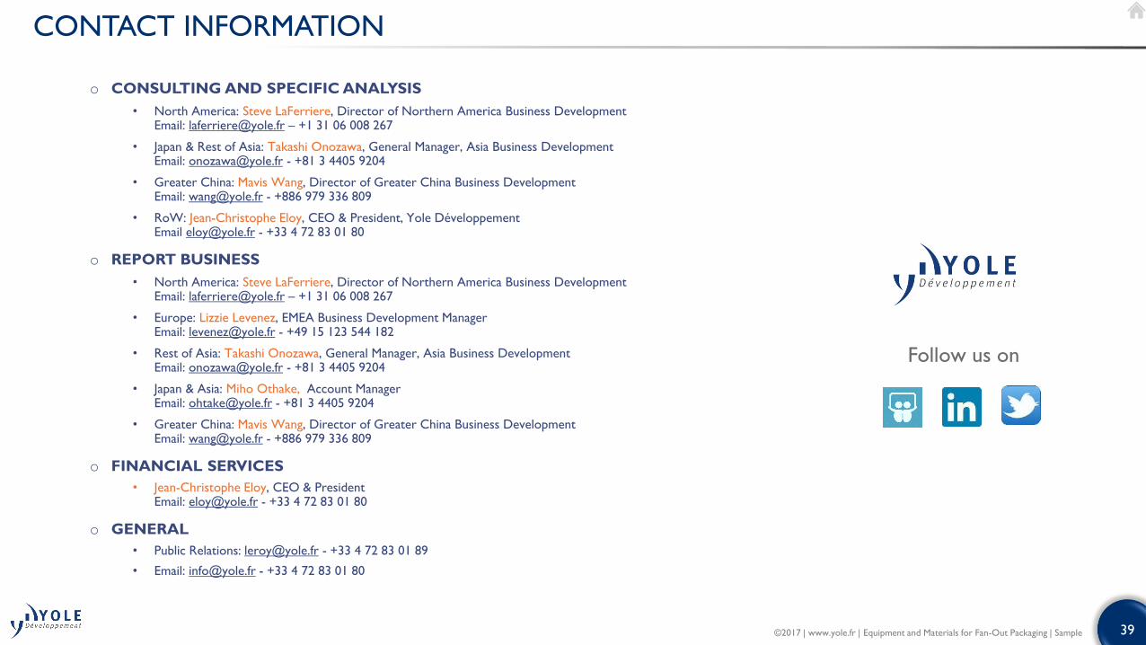
CONTACT INFORMATION
Follow us on
o CONSULTING AND SPECIFIC ANALYSIS
• North America: Steve LaFerriere, Director of Northern America Business DevelopmentEmail: [email protected] – +1 31 06 008 267
• Japan & Rest of Asia: Takashi Onozawa, General Manager, Asia Business DevelopmentEmail: [email protected] - +81 3 4405 9204
• Greater China: Mavis Wang, Director of Greater China Business DevelopmentEmail: [email protected] - +886 979 336 809
• RoW: Jean-Christophe Eloy, CEO & President, Yole DéveloppementEmail [email protected] - +33 4 72 83 01 80
o REPORT BUSINESS
• North America: Steve LaFerriere, Director of Northern America Business DevelopmentEmail: [email protected] – +1 31 06 008 267
• Europe: Lizzie Levenez, EMEA Business Development ManagerEmail: [email protected] - +49 15 123 544 182
• Rest of Asia: Takashi Onozawa, General Manager, Asia Business DevelopmentEmail: [email protected] - +81 3 4405 9204
• Japan & Asia: Miho Othake, Account ManagerEmail: [email protected] - +81 3 4405 9204
• Greater China: Mavis Wang, Director of Greater China Business DevelopmentEmail: [email protected] - +886 979 336 809
o FINANCIAL SERVICES
• Jean-Christophe Eloy, CEO & PresidentEmail: [email protected] - +33 4 72 83 01 80
o GENERAL
• Public Relations: [email protected] - +33 4 72 83 01 89
• Email: [email protected] - +33 4 72 83 01 80