description typical applications pcie clocking
TRANSCRIPT
1©2020 Renesas Electronics Corporation October 29, 2020
DescriptionThe 9FGV1001C / 9FGV1005C are members of the Renesas PhiClock™ programmable clock generator family. The devices are optimized for low phase noise in non-spread spectrum applications such as Ethernet or PCI Express. Four user-defined configurations may be selected via two hardware select pins or two I2C bits, allowing easy software selection of the desired configuration.
Typical Applications▪ High-performance Computing (HPC)▪ Enterprise Storage including eSSDs▪ 10G / 25G / 100G Ethernet▪ Data Center Accelerators▪ Multiple XO replacement
PCIe Clocking Architectures▪ Common Clocked (CC)▪ Independent Reference without spread spectrum (SRnS)
Output Features▪ 9FGV1001: 4 programmable output pairs plus 2 REF outputs▪ 9FGV1005: 2 programmable output pairs plus 1 REF output▪ 1 integer output frequency per configuration▪ 1MHz–325MHz differential outputs▪ 1MHz–200MHz single-ended outputs
Features▪ 1.8V to 3.3V power supplies▪ Individual 1.8V to 3.3V VDDO for each output pair▪ Supports HCSL, LVDS and LVCMOS I/O standards▪ HCSL utilizes Renesas’ LP-HCSL technology for improved
performance, lower power and higher integration:• Programmable output impedance of 85Ω or 100Ω
▪ Supports LVPECL and CML logic with easy AC coupling. See application note AN-891 for alternate terminations
▪ On-board OTP supports up to 4 complete configurations▪ Configuration selected via strapping pins or I2C▪ Internal crystal load capacitors▪ < 125mW at 1.8V, LP-HCSL outputs at 100MHz (9FGV1001C)▪ < 100mW at 1.8V, LP-HCSL outputs at 100MHz (9FGV1005C)▪ 4 programmable I2C addresses: D0, D2, D4, D6▪ Easily configured with Renesas Timing Commander™ software
or Web Configuration tool▪ 4 × 4 mm 24-VFQFPN (9FGV1001)▪ 3 × 3 mm 16-LGA (9FGV1005)▪ Integrated crystal option available
Key Specifications▪ 261fs RMS 12kHz–20MHz typical phase jitter at 156.25M Hz▪ PCIe Gen5 jitter (CC) < 0.08ps RMS▪ PCIe Gen5 jitter (SRNS) < 0.07ps RMS
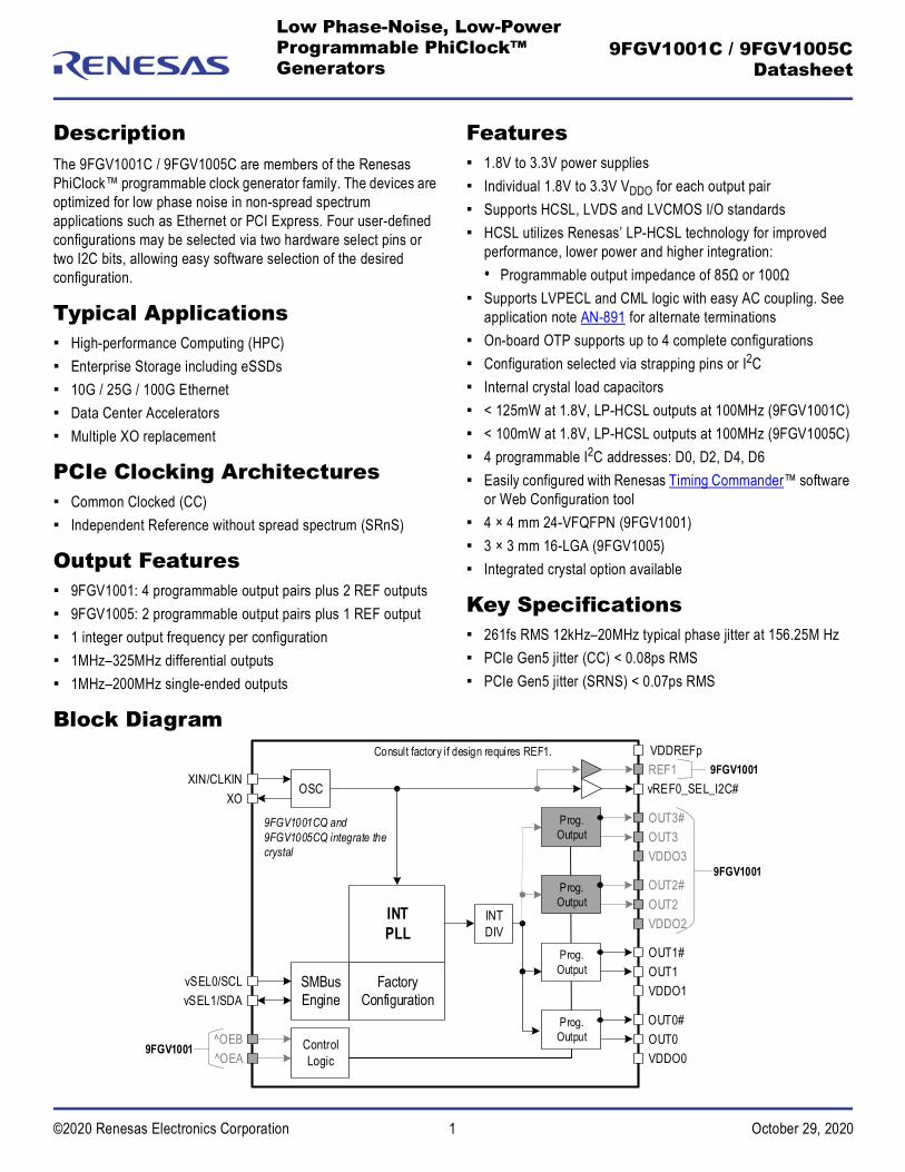
Block Diagram
OUT3#
REF1
vSEL1/SDAFactory
ConfigurationSMBus Engine
INTPLL
VDDREFp
XO
XIN/CLKIN
^OEA
vSEL0/SCL
OUT3
OUT0
OUT0#
Control Logic
^OEB
vREF0_SEL_I2C#OSC
VDDO3
INTDIV
OUT2#
OUT2
OUT1#
OUT1
VDDO2
VDDO1
VDDO0
9FGV1001CQ and 9FGV1005CQ integrate the crystal
9FGV1001
9FGV1001
Prog.Output
Prog.Output
Prog.Output
Prog.Output
9FGV1001
Consult factory if design requires REF1.
9FGV1001C / 9FGV1005CDatasheet
Low Phase-Noise, Low-Power Programmable PhiClock™ Generators
2©2020 Renesas Electronics Corporation October 29, 2020
9FGV1001C / 9FGV1005C Datasheet
ContentsDescription . . . . . . . . . . . . . . . . . . . . . . . . . . . . . . . . . . . . . . . . . . . . . . . . . . . . . . . . . . . . . . . . . . . . . . . . . . . . . . . . . . . . . . . . . . . . . . . . . . . . . . 1Typical Applications . . . . . . . . . . . . . . . . . . . . . . . . . . . . . . . . . . . . . . . . . . . . . . . . . . . . . . . . . . . . . . . . . . . . . . . . . . . . . . . . . . . . . . . . . . . . . . . 1PCIe Clocking Architectures. . . . . . . . . . . . . . . . . . . . . . . . . . . . . . . . . . . . . . . . . . . . . . . . . . . . . . . . . . . . . . . . . . . . . . . . . . . . . . . . . . . . . . . . . 1Output Features . . . . . . . . . . . . . . . . . . . . . . . . . . . . . . . . . . . . . . . . . . . . . . . . . . . . . . . . . . . . . . . . . . . . . . . . . . . . . . . . . . . . . . . . . . . . . . . . . . 1Features . . . . . . . . . . . . . . . . . . . . . . . . . . . . . . . . . . . . . . . . . . . . . . . . . . . . . . . . . . . . . . . . . . . . . . . . . . . . . . . . . . . . . . . . . . . . . . . . . . . . . . . . 1Key Specifications . . . . . . . . . . . . . . . . . . . . . . . . . . . . . . . . . . . . . . . . . . . . . . . . . . . . . . . . . . . . . . . . . . . . . . . . . . . . . . . . . . . . . . . . . . . . . . . . 1Block Diagram . . . . . . . . . . . . . . . . . . . . . . . . . . . . . . . . . . . . . . . . . . . . . . . . . . . . . . . . . . . . . . . . . . . . . . . . . . . . . . . . . . . . . . . . . . . . . . . . . . . 19FGV1001 Pin Assignments and Descriptions . . . . . . . . . . . . . . . . . . . . . . . . . . . . . . . . . . . . . . . . . . . . . . . . . . . . . . . . . . . . . . . . . . . . . . . . . . 39FGV1005 Pin Assignments and Descriptions . . . . . . . . . . . . . . . . . . . . . . . . . . . . . . . . . . . . . . . . . . . . . . . . . . . . . . . . . . . . . . . . . . . . . . . . . . 5Phase Noise Plots . . . . . . . . . . . . . . . . . . . . . . . . . . . . . . . . . . . . . . . . . . . . . . . . . . . . . . . . . . . . . . . . . . . . . . . . . . . . . . . . . . . . . . . . . . . . . . . . 7Absolute Maximum Ratings . . . . . . . . . . . . . . . . . . . . . . . . . . . . . . . . . . . . . . . . . . . . . . . . . . . . . . . . . . . . . . . . . . . . . . . . . . . . . . . . . . . . . . . . . 8Recommended Operating Conditions . . . . . . . . . . . . . . . . . . . . . . . . . . . . . . . . . . . . . . . . . . . . . . . . . . . . . . . . . . . . . . . . . . . . . . . . . . . . . . . . . 8Electrical Characteristics . . . . . . . . . . . . . . . . . . . . . . . . . . . . . . . . . . . . . . . . . . . . . . . . . . . . . . . . . . . . . . . . . . . . . . . . . . . . . . . . . . . . . . . . . . . 9I2C Bus Characteristics . . . . . . . . . . . . . . . . . . . . . . . . . . . . . . . . . . . . . . . . . . . . . . . . . . . . . . . . . . . . . . . . . . . . . . . . . . . . . . . . . . . . . . . . . . . 15Test Loads . . . . . . . . . . . . . . . . . . . . . . . . . . . . . . . . . . . . . . . . . . . . . . . . . . . . . . . . . . . . . . . . . . . . . . . . . . . . . . . . . . . . . . . . . . . . . . . . . . . . . 16Crystal Characteristics . . . . . . . . . . . . . . . . . . . . . . . . . . . . . . . . . . . . . . . . . . . . . . . . . . . . . . . . . . . . . . . . . . . . . . . . . . . . . . . . . . . . . . . . . . . . 18Package Outline Drawings . . . . . . . . . . . . . . . . . . . . . . . . . . . . . . . . . . . . . . . . . . . . . . . . . . . . . . . . . . . . . . . . . . . . . . . . . . . . . . . . . . . . . . . . . 18Thermal Characteristics . . . . . . . . . . . . . . . . . . . . . . . . . . . . . . . . . . . . . . . . . . . . . . . . . . . . . . . . . . . . . . . . . . . . . . . . . . . . . . . . . . . . . . . . . . . 19Marking Diagrams . . . . . . . . . . . . . . . . . . . . . . . . . . . . . . . . . . . . . . . . . . . . . . . . . . . . . . . . . . . . . . . . . . . . . . . . . . . . . . . . . . . . . . . . . . . . . . . 20Standard Configurations. . . . . . . . . . . . . . . . . . . . . . . . . . . . . . . . . . . . . . . . . . . . . . . . . . . . . . . . . . . . . . . . . . . . . . . . . . . . . . . . . . . . . . . . . . . 20Ordering Information . . . . . . . . . . . . . . . . . . . . . . . . . . . . . . . . . . . . . . . . . . . . . . . . . . . . . . . . . . . . . . . . . . . . . . . . . . . . . . . . . . . . . . . . . . . . . 21Revision History . . . . . . . . . . . . . . . . . . . . . . . . . . . . . . . . . . . . . . . . . . . . . . . . . . . . . . . . . . . . . . . . . . . . . . . . . . . . . . . . . . . . . . . . . . . . . . . . . 22
3©2020 Renesas Electronics Corporation October 29, 2020
9FGV1001C / 9FGV1005C Datasheet
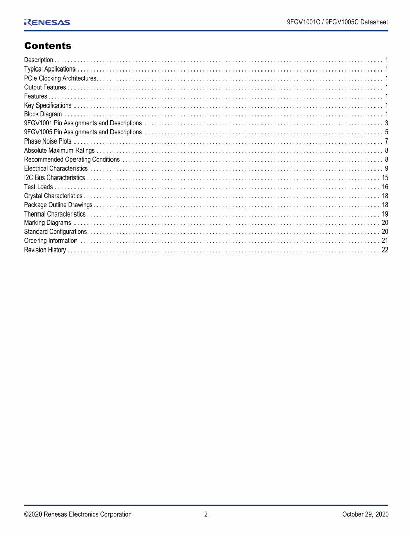
9FGV1001 Pin Assignments and DescriptionsFigure 1. Pin Assignments for 9FGV1001C 4 x 4 mm 24-VFQFPN and 24-LGA Packages – Top View
Table 1. 9FGV1001C Pin Descriptions[a]
Number Name Type Description
1[b] XIN/CLKIN Input Crystal input or reference clock input.
2[b] XO Output Crystal output.
3 REF1 Output LVCMOS reference output.
4 vSEL0/SCL Input Select pin for internal frequency configurations/I2C clock pin. Function is determined by state of SEL_I2C# upon power-up. This pin has an internal pull-down.
5 vSEL1/SDA I/O Select pin for internal frequency configurations/I2C data pin. Function is determined by state of SEL_I2C# upon power-up. This pin has an internal pull-down.
6 ^OEA Input Active high input for enabling outputs. This pin has an internal pull-up resistor.0 = disable outputs, 1 = enable outputs.
7 VDDDp Power Digital power. Connect to 1.8V, 2.5V or 3.3V.
8 ^OEB Input Active high input for enabling outputs. This pin has an internal pull-up resistor.0 = disable outputs, 1 = enable outputs.
9 OTP_VPP Power Voltage for programming OTP. During normal operation, this pin should be connected to the same power rail as VDDD.
10 OUT0# Output Complementary output clock 0.
11 OUT0 Output Output clock 0.
12 VDDO0 Power Power supply for output 0.
13 OUT1# Output Complementary output clock 1.
VDD
REF
p
vREF
0_SE
L_I2
C#
VDD
Ap
VDD
O3
OU
T3#
OU
T3
24 23 22 21 20 19
XIN/CLKIN 1 18 VDDO2
XO 2 17 OUT2
REF1 3 16 OUT2#
vSEL0/SCL 4 15 VDDO1
vSEL1/SDA 5 14 OUT1
^OEA 6 13 OUT1#
7 8 9 10 11 12
VDD
Dp
^OEB
OTP
_VPP
OU
T0#
OU
T0
VDD
O0
^ prefix indicates internal pull-up resistorv prefix indicates internal pull-down resistor
9FGV1001CConnect
EPAD to GND
4 × 4 mm 24-VFQFPN, 0.5mm pitch
VDD
REF
p
vREF
0_SE
L_I2
C#
VDD
Ap
VDD
O3
OU
T3#
OU
T3
24 23 22 21 20 19
NC 1 18 VDDO2
NC 2 17 OUT2
REF1 3 16 OUT2#
vSEL0/SCL 4 15 VDDO1
vSEL1/SDA 5 14 OUT1
^OEA 6 13 OUT1#
7 8 9 10 11 12
VDD
Dp
^OEB
OTP
_VPP
OU
T0#
OU
T0
VDD
O0
9FGV1001CQConnect
EPAD to GND
4 × 4 mm 24-LGA, 0.5mm pitch^ prefix indicates internal pull-up resistor
v prefix indicates internal pull-down resistor
4©2020 Renesas Electronics Corporation October 29, 2020
9FGV1001C / 9FGV1005C Datasheet
14 OUT1 Output Output clock 1.
15 VDDO1 Power Power supply for output 1.
16 OUT2# Output Complementary output clock 2.
17 OUT2 Output Output clock 2.
18 VDDO2 Power Power supply for output 2.
19 OUT3 Output Output clock 3.
20 OUT3# Output Complementary output clock 3.
21 VDDO3 Power Power supply for output 3.
22 VDDAp Power Analog power. Connect to same voltage as VDDDp, with proper filtering.
23 vREF0_SEL_I2C# Latched I/O
Latched input/LVCMOS output. At power-up, the state of this pin is latched to select the state of the I2C pins. After power-up, the pin acts as an LVCMOS reference output. This pin has an internal pull-down.1 = SEL0/SEL1.0 = SCL/SDA.
24 VDDREFp Power Power supply for REF outputs and the internal XO. Nominal voltages are 1.8V, 2.5V or 3.3V.
25 EPAD GND Connect to ground.
[a] Unused outputs can be programmed off and left floating. Output supplies VDDREF and VDDO2 have to be connected. If OUT0 is used, VDDO1 must also be connected.
[b] These pins are 'No Connect' on 9FGV1001CQ integrated quartz versions and should have no stubs.
Table 2. 9FGV1001 OE Mapping
OE[B:A] OUT0 OUT1 OUT2 OUT3 REF0 REF1
00 Running Stopped Stopped Stopped Running Running
01 Running Running Stopped Stopped Running Running
10 Running Running Running Stopped Running Running
11 Running Running Running Running Running Running
Table 1. 9FGV1001C Pin Descriptions[a] (Cont.)
Number Name Type Description
5©2020 Renesas Electronics Corporation October 29, 2020
9FGV1001C / 9FGV1005C Datasheet
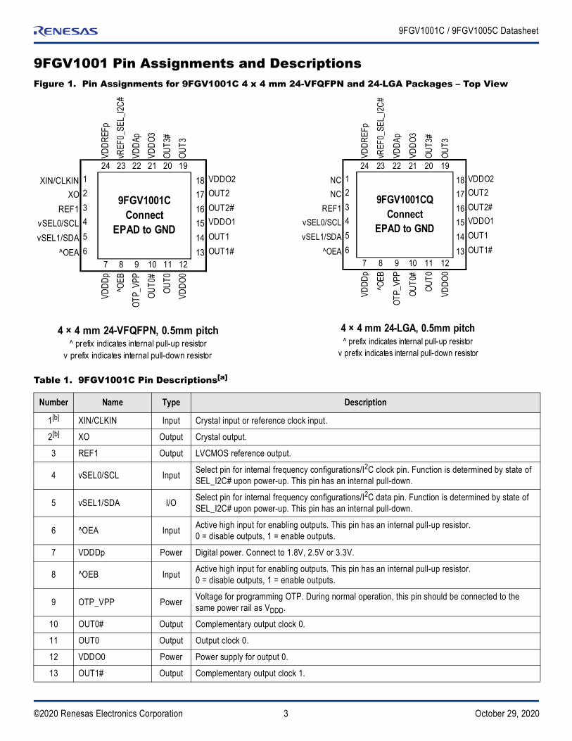
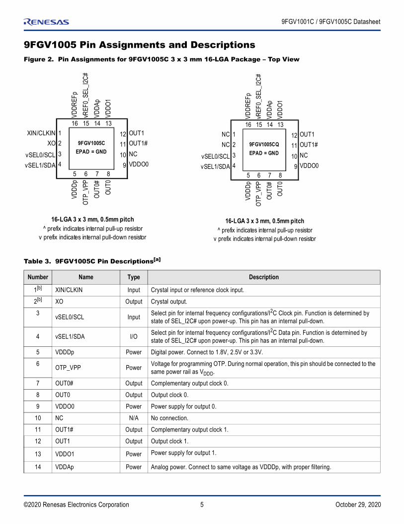
9FGV1005 Pin Assignments and DescriptionsFigure 2. Pin Assignments for 9FGV1005C 3 x 3 mm 16-LGA Package – Top View
Table 3. 9FGV1005C Pin Descriptions[a]
Number Name Type Description
1[b] XIN/CLKIN Input Crystal input or reference clock input.
2[b] XO Output Crystal output.
3 vSEL0/SCL Input Select pin for internal frequency configurations/I2C Clock pin. Function is determined by state of SEL_I2C# upon power-up. This pin has an internal pull-down.
4 vSEL1/SDA I/O Select pin for internal frequency configurations/I2C Data pin. Function is determined by state of SEL_I2C# upon power-up. This pin has an internal pull-down.
5 VDDDp Power Digital power. Connect to 1.8V, 2.5V or 3.3V.
6 OTP_VPP Power Voltage for programming OTP. During normal operation, this pin should be connected to the same power rail as VDDD.
7 OUT0# Output Complementary output clock 0.
8 OUT0 Output Output clock 0.
9 VDDO0 Power Power supply for output 0.
10 NC N/A No connection.
11 OUT1# Output Complementary output clock 1.
12 OUT1 Output Output clock 1.
13 VDDO1 Power Power supply for output 1.
14 VDDAp Power Analog power. Connect to same voltage as VDDDp, with proper filtering.
VDDR
EFp
vREF
0_SE
L_I2
C#
VDDA
p
VDDO
1
16 15 14 13
XIN/CLKIN 1 12 OUT1
XO 2 11 OUT1#
vSEL0/SCL 3 10 NC
vSEL1/SDA 4 9 VDDO0
5 6 7 8
VDD
Dp
OTP
_VPP
OUT
0#
OU
T0
^ prefix indicates internal pull-up resistorv prefix indicates internal pull-down resistor
9FGV1005C
EPAD = GND
16-LGA 3 x 3 mm, 0.5mm pitch
VDD
REF
p
vREF
0_SE
L_I2
C#
VDD
Ap
VDD
O1
16 15 14 13
NC 1 12 OUT1
NC 2 11 OUT1#
vSEL0/SCL 3 10 NC
vSEL1/SDA 4 9 VDDO0
5 6 7 8
VDD
Dp
OTP
_VPP
OU
T0#
OU
T0
^ prefix indicates internal pull-up resistorv prefix indicates internal pull-down resistor
9FGV1005CQ
EPAD = GND
16-LGA 3 x 3 mm, 0.5mm pitch
6©2020 Renesas Electronics Corporation October 29, 2020
9FGV1001C / 9FGV1005C Datasheet
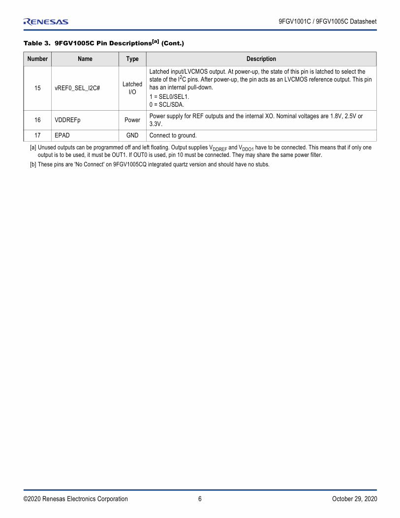
15 vREF0_SEL_I2C# Latched I/O
Latched input/LVCMOS output. At power-up, the state of this pin is latched to select the state of the I2C pins. After power-up, the pin acts as an LVCMOS reference output. This pin has an internal pull-down.1 = SEL0/SEL1.0 = SCL/SDA.
16 VDDREFp Power Power supply for REF outputs and the internal XO. Nominal voltages are 1.8V, 2.5V or 3.3V.
17 EPAD GND Connect to ground.
[a] Unused outputs can be programmed off and left floating. Output supplies VDDREF and VDDO1 have to be connected. This means that if only one output is to be used, it must be OUT1. If OUT0 is used, pin 10 must be connected. They may share the same power filter.
[b] These pins are 'No Connect' on 9FGV1005CQ integrated quartz version and should have no stubs.
Table 3. 9FGV1005C Pin Descriptions[a] (Cont.)
Number Name Type Description
7©2020 Renesas Electronics Corporation October 29, 2020
9FGV1001C / 9FGV1005C Datasheet
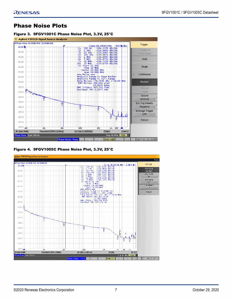
Phase Noise PlotsFigure 3. 9FGV1001C Phase Noise Plot, 3.3V, 25°C
Figure 4. 9FGV1005C Phase Noise Plot, 3.3V, 25°C
8©2020 Renesas Electronics Corporation October 29, 2020
9FGV1001C / 9FGV1005C Datasheet
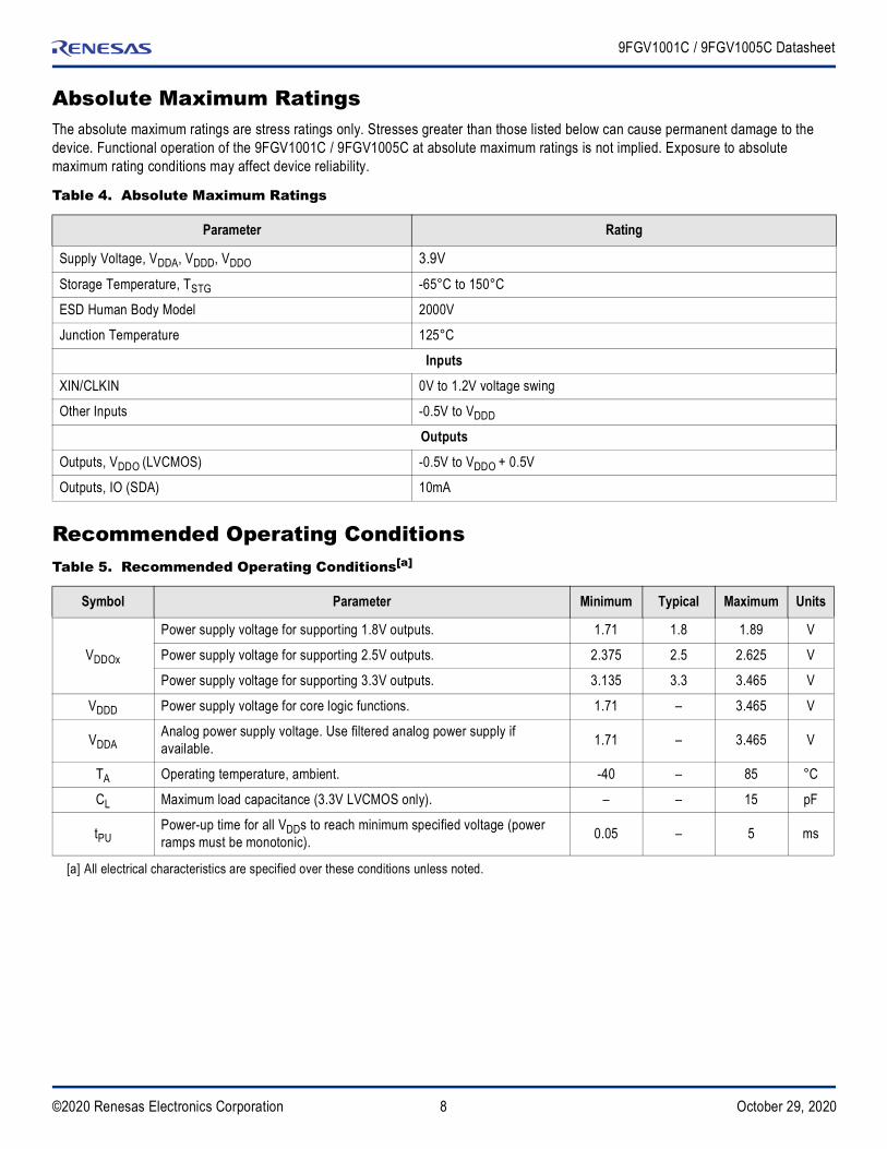
Absolute Maximum RatingsThe absolute maximum ratings are stress ratings only. Stresses greater than those listed below can cause permanent damage to the device. Functional operation of the 9FGV1001C / 9FGV1005C at absolute maximum ratings is not implied. Exposure to absolute maximum rating conditions may affect device reliability.
Recommended Operating Conditions
Table 4. Absolute Maximum Ratings
Parameter Rating
Supply Voltage, VDDA, VDDD, VDDO 3.9VStorage Temperature, TSTG -65°C to 150°C
ESD Human Body Model 2000V
Junction Temperature 125°C
InputsXIN/CLKIN 0V to 1.2V voltage swing
Other Inputs -0.5V to VDDD
OutputsOutputs, VDDO (LVCMOS) -0.5V to VDDO + 0.5V
Outputs, IO (SDA) 10mA
Table 5. Recommended Operating Conditions[a]
[a] All electrical characteristics are specified over these conditions unless noted.
Symbol Parameter Minimum Typical Maximum Units
VDDOx
Power supply voltage for supporting 1.8V outputs. 1.71 1.8 1.89 V
Power supply voltage for supporting 2.5V outputs. 2.375 2.5 2.625 V
Power supply voltage for supporting 3.3V outputs. 3.135 3.3 3.465 V
VDDD Power supply voltage for core logic functions. 1.71 – 3.465 V
VDDAAnalog power supply voltage. Use filtered analog power supply if available. 1.71 – 3.465 V
TA Operating temperature, ambient. -40 – 85 °C
CL Maximum load capacitance (3.3V LVCMOS only). – – 15 pF
tPUPower-up time for all VDDs to reach minimum specified voltage (power ramps must be monotonic). 0.05 – 5 ms
9©2020 Renesas Electronics Corporation October 29, 2020
9FGV1001C / 9FGV1005C Datasheet
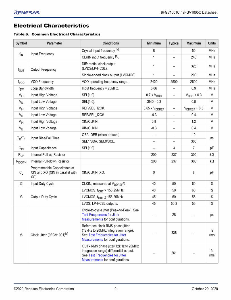
Electrical CharacteristicsTable 6. Common Electrical Characteristics
Symbol Parameter Conditions Minimum Typical Maximum Units
fIN Input FrequencyCrystal input frequency [a]. 8 – 50 MHz
CLKIN input frequency [b]. 1 – 240 MHz
fOUT Output FrequencyDifferential clock output (LVDS/LP-HCSL). 1 – 325 MHz
Single-ended clock output (LVCMOS). 1 – 200 MHz
fVCO VCO Frequency VCO operating frequency range. 2400 2500 2600 MHz
fBW Loop Bandwidth Input frequency = 25MHz. 0.06 – 0.9 MHz
VIH Input High Voltage SEL[1:0]. 0.7 x VDDD – VDDD + 0.3 V
VIL Input Low Voltage SEL[1:0]. GND - 0.3 – 0.8 V
VIH Input High Voltage REF/SEL_I2C#. 0.65 x VDDREF – VDDREF + 0.3 V
VIL Input Low Voltage REF/SEL_I2C#. -0.3 – 0.4 V
VIH Input High Voltage XIN/CLKIN. 0.8 – 1.2 V
VIL Input Low Voltage XIN/CLKIN. -0.3 – 0.4 V
TR/TF Input Rise/Fall TimeOEA, OEB (when present). – – 10
nsSEL1/SDA, SEL0/SCL. – – 300
CIN Input Capacitance SEL[1:0]. – 3 7 pF
RUP Internal Pull-up Resistor 200 237 300 kΩ
RDOWN Internal Pull-down Resistor 200 237 300 kΩ
CL
Programmable Capacitance at XIN and XO (XIN in parallel with XO)
XIN/CLKIN, XO. 0 8 pF
t2 Input Duty Cycle CLKIN, measured at VDDREF/2. 40 50 60 %
t3 Output Duty Cycle
LVCMOS, fOUT > 156.25MHz. 40 50 60 %
LVCMOS, fOUT < 156.25MHz. 45 50 55 %
LVDS, LP-HCSL outputs. 45 50.2 55 %
t6 Clock Jitter (9FGV1001)[c]
Cycle-to-cycle jitter (Peak-to-Peak), See Test Frequencies for Jitter Measurements for configurations.
– 28 – ps
Reference clock RMS phase jitter (12kHz to 20MHz integration range). See Test Frequencies for Jitter Measurements for configurations.
– 338 – fs rms
OUTx RMS phase jitter(12kHz to 20MHz integration range) differential output. See Test Frequencies for Jitter Measurements for configurations.
– 261 – fs rms
10©2020 Renesas Electronics Corporation October 29, 2020
9FGV1001C / 9FGV1005C Datasheet
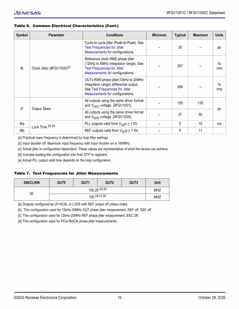
t6 Clock Jitter (9FGV1005)[c]
Cycle-to-cycle jitter (Peak-to-Peak). See Test Frequencies for Jitter Measurements for configurations.
– 30 – ps
Reference clock RMS phase jitter (12kHz to 5MHz integration range). See Test Frequencies for Jitter Measurements for configurations.
– 357 – fs rms
OUTx RMS phase jitter(12kHz to 20MHz integration range) differential output. See Test Frequencies for Jitter Measurements for configurations.
– 284 – fs rms
t7 Output Skew
All outputs using the same driver format and VDDO voltage. (9FGV1001). – 105 135
psAll outputs using the same driver format and VDDO voltage. (9FGV1005). – 37 50
t8aLock Time [d] [e] PLL outputs valid from VDDs > 1.5V. – 5 10 ms
t8b REF outputs valid from VDDs > 1.5V. – 5 11
[a] Practical lower frequency is determined by loop filter settings.[b] Input doubler off. Maximum input frequency with input doubler on is 160MHz.[c] Actual jitter is configuration dependent. These values are representative of what the device can achieve.[d] Includes loading the configuration bits from OTP to registers.[e] Actual PLL output valid time depends on the loop configuration.
Table 7. Test Frequencies for Jitter Measurements
XIN/CLKIN OUT0 OUT1 OUT2 OUT3 Unit
50156.25 [a] [b]
[a] Outputs configured as LP-HCSL or LVDS with REF output off unless noted. [b] This configuration used for 12kHz-20MHz OUT phase jitter measurement. REF off, SSC off.
MHZ
100 [a] [c] [d]
[c] This configuration used for 12kHz-20MHz REF phase jitter measurement, SSC Off.[d] This configuration used for PCIe RefClk phase jitter measurements.
MHZ
Table 6. Common Electrical Characteristics (Cont.)
Symbol Parameter Conditions Minimum Typical Maximum Units
11©2020 Renesas Electronics Corporation October 29, 2020
9FGV1001C / 9FGV1005C Datasheet
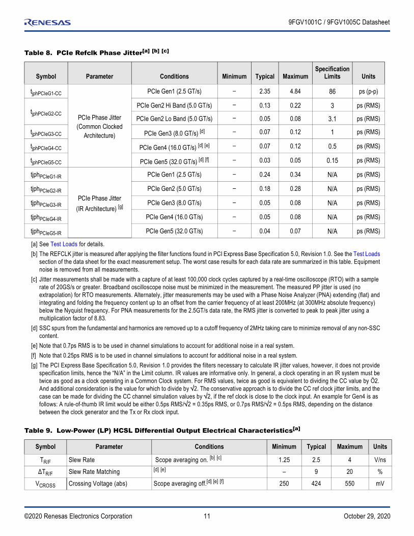
Table 8. PCIe Refclk Phase Jitter[a] [b] [c]
[a] See Test Loads for details.[b] The REFCLK jitter is measured after applying the filter functions found in PCI Express Base Specification 5.0, Revision 1.0. See the Test Loads
section of the data sheet for the exact measurement setup. The worst case results for each data rate are summarized in this table. Equipment noise is removed from all measurements.
[c] Jitter measurements shall be made with a capture of at least 100,000 clock cycles captured by a real-time oscilloscope (RTO) with a sample rate of 20GS/s or greater. Broadband oscilloscope noise must be minimized in the measurement. The measured PP jitter is used (no extrapolation) for RTO measurements. Alternately, jitter measurements may be used with a Phase Noise Analyzer (PNA) extending (flat) and integrating and folding the frequency content up to an offset from the carrier frequency of at least 200MHz (at 300MHz absolute frequency) below the Nyquist frequency. For PNA measurements for the 2.5GT/s data rate, the RMS jitter is converted to peak to peak jitter using a multiplication factor of 8.83.
Symbol Parameter Conditions Minimum Typical MaximumSpecification
Limits Units
tjphPCIeG1-CC
PCIe Phase Jitter(Common Clocked
Architecture)
PCIe Gen1 (2.5 GT/s) – 2.35 4.84 86 ps (p-p)
tjphPCIeG2-CCPCIe Gen2 Hi Band (5.0 GT/s) – 0.13 0.22 3 ps (RMS)
PCIe Gen2 Lo Band (5.0 GT/s) – 0.05 0.08 3.1 ps (RMS)
tjphPCIeG3-CC PCIe Gen3 (8.0 GT/s) [d]
[d] SSC spurs from the fundamental and harmonics are removed up to a cutoff frequency of 2MHz taking care to minimize removal of any non-SSC content.
– 0.07 0.12 1 ps (RMS)
tjphPCIeG4-CC PCIe Gen4 (16.0 GT/s) [d] [e]
[e] Note that 0.7ps RMS is to be used in channel simulations to account for additional noise in a real system.
– 0.07 0.12 0.5 ps (RMS)
tjphPCIeG5-CC PCIe Gen5 (32.0 GT/s) [d] [f]
[f] Note that 0.25ps RMS is to be used in channel simulations to account for additional noise in a real system.
– 0.03 0.05 0.15 ps (RMS)
tjphPCIeG1-IR
PCIe Phase Jitter(IR Architecture) [g]
[g] The PCI Express Base Specification 5.0, Revision 1.0 provides the filters necessary to calculate IR jitter values, however, it does not provide specification limits, hence the “N/A” in the Limit column. IR values are informative only. In general, a clock operating in an IR system must be twice as good as a clock operating in a Common Clock system. For RMS values, twice as good is equivalent to dividing the CC value by Ö2. And additional consideration is the value for which to divide by 2. The conservative approach is to divide the CC ref clock jitter limits, and the case can be made for dividing the CC channel simulation values by 2, if the ref clock is close to the clock input. An example for Gen4 is as follows: A rule-of-thumb IR limit would be either 0.5ps RMS/2 = 0.35ps RMS, or 0.7ps RMS/2 = 0.5ps RMS, depending on the distance between the clock generator and the Tx or Rx clock input.
PCIe Gen1 (2.5 GT/s) – 0.24 0.34 N/A ps (RMS)
tjphPCIeG2-IR PCIe Gen2 (5.0 GT/s) – 0.18 0.28 N/A ps (RMS)
tjphPCIeG3-IR PCIe Gen3 (8.0 GT/s) – 0.05 0.08 N/A ps (RMS)
tjphPCIeG4-IR PCIe Gen4 (16.0 GT/s) – 0.05 0.08 N/A ps (RMS)
tjphPCIeG5-IR PCIe Gen5 (32.0 GT/s) – 0.04 0.07 N/A ps (RMS)
Table 9. Low-Power (LP) HCSL Differential Output Electrical Characteristics[a]
Symbol Parameter Conditions Minimum Typical Maximum Units
TR/F Slew Rate Scope averaging on. [b] [c] 1.25 2.5 4 V/ns
ΔTR/F Slew Rate Matching [d] [e] – 9 20 %
VCROSS Crossing Voltage (abs) Scope averaging off.[d] [e] [f] 250 424 550 mV
12©2020 Renesas Electronics Corporation October 29, 2020
9FGV1001C / 9FGV1005C Datasheet
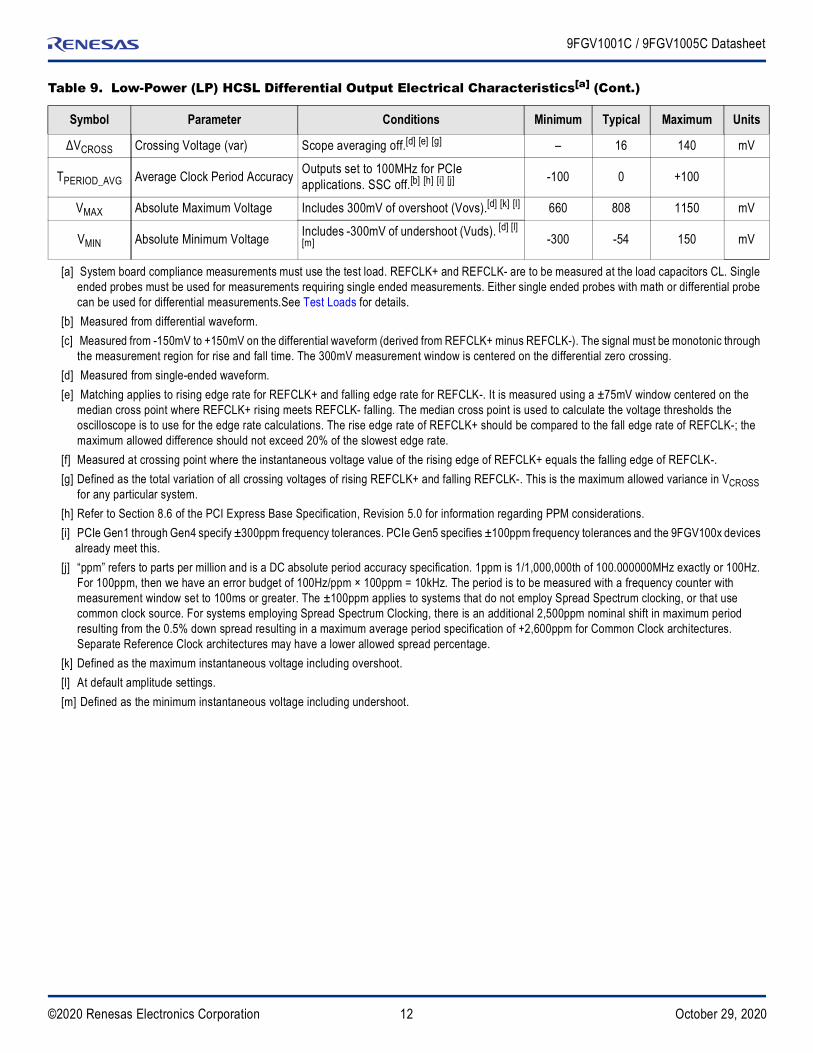
ΔVCROSS Crossing Voltage (var) Scope averaging off.[d] [e] [g] – 16 140 mV
TPERIOD_AVG Average Clock Period Accuracy Outputs set to 100MHz for PCIe applications. SSC off.[b] [h] [i] [j] -100 0 +100
VMAX Absolute Maximum Voltage Includes 300mV of overshoot (Vovs).[d] [k] [l] 660 808 1150 mV
VMIN Absolute Minimum Voltage Includes -300mV of undershoot (Vuds). [d] [l] [m] -300 -54 150 mV
[a] System board compliance measurements must use the test load. REFCLK+ and REFCLK- are to be measured at the load capacitors CL. Single ended probes must be used for measurements requiring single ended measurements. Either single ended probes with math or differential probe can be used for differential measurements.See Test Loads for details.
[b] Measured from differential waveform.[c] Measured from -150mV to +150mV on the differential waveform (derived from REFCLK+ minus REFCLK-). The signal must be monotonic through
the measurement region for rise and fall time. The 300mV measurement window is centered on the differential zero crossing.[d] Measured from single-ended waveform.[e] Matching applies to rising edge rate for REFCLK+ and falling edge rate for REFCLK-. It is measured using a ±75mV window centered on the
median cross point where REFCLK+ rising meets REFCLK- falling. The median cross point is used to calculate the voltage thresholds the oscilloscope is to use for the edge rate calculations. The rise edge rate of REFCLK+ should be compared to the fall edge rate of REFCLK-; the maximum allowed difference should not exceed 20% of the slowest edge rate.
[f] Measured at crossing point where the instantaneous voltage value of the rising edge of REFCLK+ equals the falling edge of REFCLK-.[g] Defined as the total variation of all crossing voltages of rising REFCLK+ and falling REFCLK-. This is the maximum allowed variance in VCROSS
for any particular system.[h] Refer to Section 8.6 of the PCI Express Base Specification, Revision 5.0 for information regarding PPM considerations.[i] PCIe Gen1 through Gen4 specify ±300ppm frequency tolerances. PCIe Gen5 specifies ±100ppm frequency tolerances and the 9FGV100x devices
already meet this.[j] “ppm” refers to parts per million and is a DC absolute period accuracy specification. 1ppm is 1/1,000,000th of 100.000000MHz exactly or 100Hz.
For 100ppm, then we have an error budget of 100Hz/ppm × 100ppm = 10kHz. The period is to be measured with a frequency counter with measurement window set to 100ms or greater. The ±100ppm applies to systems that do not employ Spread Spectrum clocking, or that use common clock source. For systems employing Spread Spectrum Clocking, there is an additional 2,500ppm nominal shift in maximum period resulting from the 0.5% down spread resulting in a maximum average period specification of +2,600ppm for Common Clock architectures. Separate Reference Clock architectures may have a lower allowed spread percentage.
[k] Defined as the maximum instantaneous voltage including overshoot.[l] At default amplitude settings.[m] Defined as the minimum instantaneous voltage including undershoot.
Table 9. Low-Power (LP) HCSL Differential Output Electrical Characteristics[a] (Cont.)
Symbol Parameter Conditions Minimum Typical Maximum Units
13©2020 Renesas Electronics Corporation October 29, 2020
9FGV1001C / 9FGV1005C Datasheet
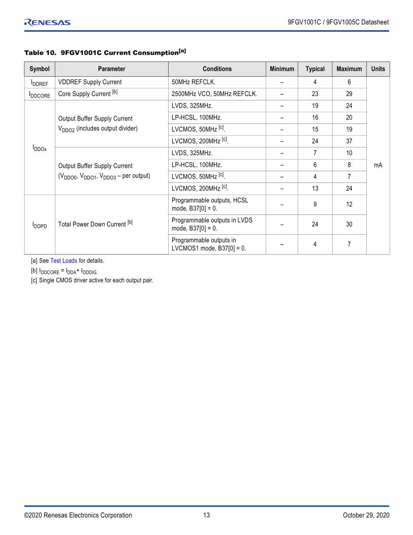
Table 10. 9FGV1001C Current Consumption[a]
[a] See Test Loads for details.
Symbol Parameter Conditions Minimum Typical Maximum Units
IDDREF VDDREF Supply Current 50MHz REFCLK. – 4 6
mA
IDDCORE Core Supply Current [b]
[b] IDDCORE = IDDA+ IDDDIG.
2500MHz VCO, 50MHz REFCLK. – 23 29
IDDOx
Output Buffer Supply CurrentVDDO2 (includes output divider)
LVDS, 325MHz. – 19 24
LP-HCSL, 100MHz. – 16 20
LVCMOS, 50MHz [c].
[c] Single CMOS driver active for each output pair.
– 15 19
LVCMOS, 200MHz [c]. – 24 37
Output Buffer Supply Current(VDDO0, VDDO1, VDDO3 – per output)
LVDS, 325MHz. – 7 10
LP-HCSL, 100MHz. – 6 8
LVCMOS, 50MHz [c]. – 4 7
LVCMOS, 200MHz [c]. – 13 24
IDDPD Total Power Down Current [b]
Programmable outputs, HCSL mode, B37[0] = 0. – 9 12
Programmable outputs in LVDS mode, B37[0] = 0. – 24 30
Programmable outputs in LVCMOS1 mode, B37[0] = 0. – 4 7
14©2020 Renesas Electronics Corporation October 29, 2020
9FGV1001C / 9FGV1005C Datasheet
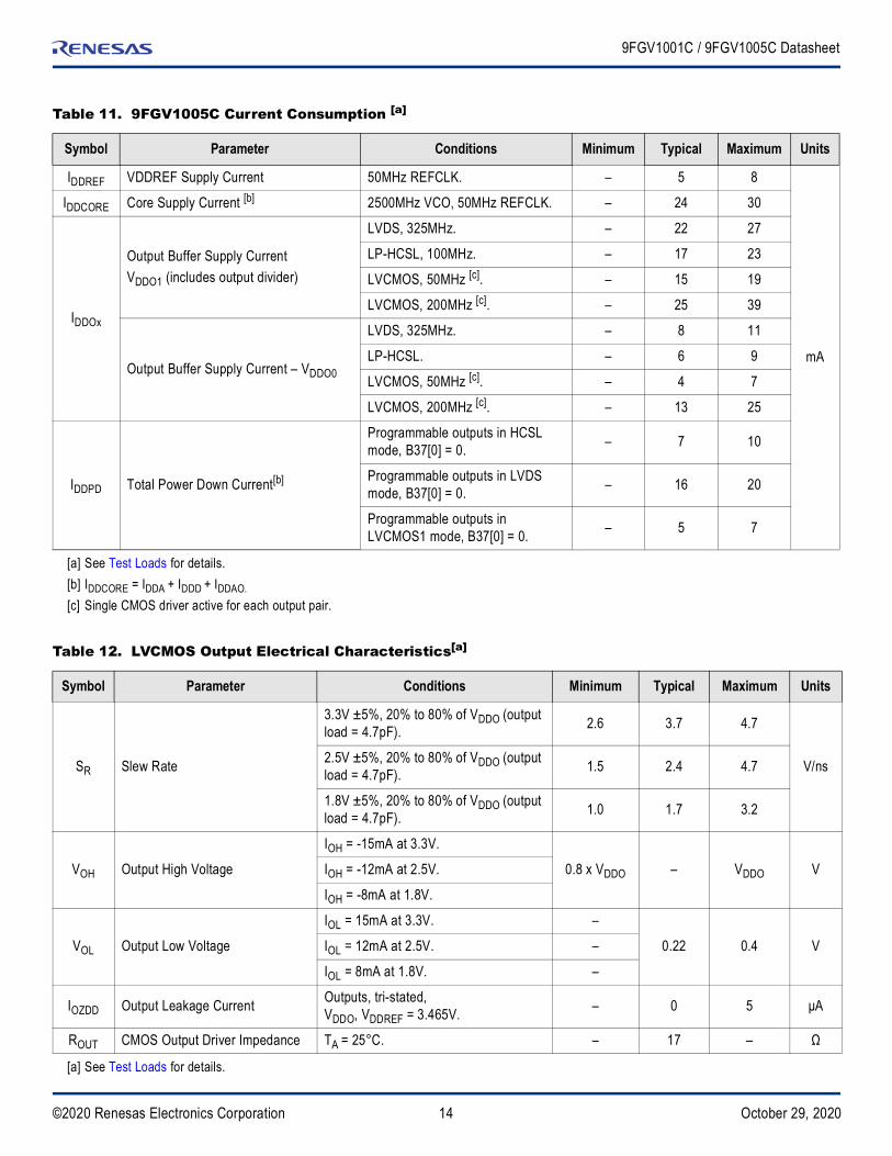
Table 11. 9FGV1005C Current Consumption [a]
[a] See Test Loads for details.
Symbol Parameter Conditions Minimum Typical Maximum Units
IDDREF VDDREF Supply Current 50MHz REFCLK. – 5 8
mA
IDDCORE Core Supply Current [b]
[b] IDDCORE = IDDA + IDDD + IDDAO.
2500MHz VCO, 50MHz REFCLK. – 24 30
IDDOx
Output Buffer Supply CurrentVDDO1 (includes output divider)
LVDS, 325MHz. – 22 27
LP-HCSL, 100MHz. – 17 23
LVCMOS, 50MHz [c].
[c] Single CMOS driver active for each output pair.
– 15 19
LVCMOS, 200MHz [c]. – 25 39
Output Buffer Supply Current – VDDO0
LVDS, 325MHz. – 8 11
LP-HCSL. – 6 9
LVCMOS, 50MHz [c]. – 4 7
LVCMOS, 200MHz [c]. – 13 25
IDDPD Total Power Down Current[b]
Programmable outputs in HCSL mode, B37[0] = 0. – 7 10
Programmable outputs in LVDS mode, B37[0] = 0. – 16 20
Programmable outputs in LVCMOS1 mode, B37[0] = 0. – 5 7
Table 12. LVCMOS Output Electrical Characteristics[a]
[a] See Test Loads for details.
Symbol Parameter Conditions Minimum Typical Maximum Units
SR Slew Rate
3.3V ±5%, 20% to 80% of VDDO (output load = 4.7pF). 2.6 3.7 4.7
V/ns2.5V ±5%, 20% to 80% of VDDO (output load = 4.7pF). 1.5 2.4 4.7
1.8V ±5%, 20% to 80% of VDDO (output load = 4.7pF). 1.0 1.7 3.2
VOH Output High Voltage
IOH = -15mA at 3.3V.
0.8 x VDDO – VDDO VIOH = -12mA at 2.5V.
IOH = -8mA at 1.8V.
VOL Output Low Voltage
IOL = 15mA at 3.3V. –
0.22 0.4 VIOL = 12mA at 2.5V. –
IOL = 8mA at 1.8V. –
IOZDD Output Leakage Current Outputs, tri-stated, VDDO, VDDREF = 3.465V. – 0 5 μA
ROUT CMOS Output Driver Impedance TA = 25°C. – 17 – Ω
15©2020 Renesas Electronics Corporation October 29, 2020
9FGV1001C / 9FGV1005C Datasheet
I2C Bus Characteristics
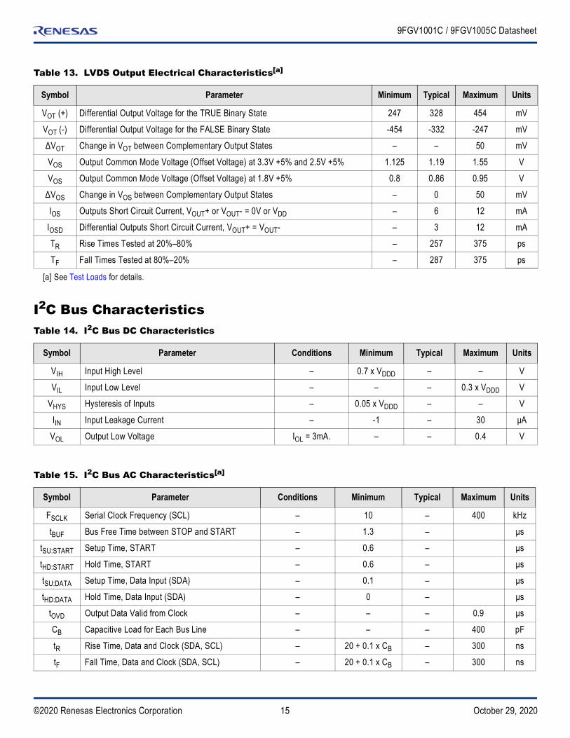
Table 13. LVDS Output Electrical Characteristics[a]
[a] See Test Loads for details.
Symbol Parameter Minimum Typical Maximum Units
VOT (+) Differential Output Voltage for the TRUE Binary State 247 328 454 mV
VOT (-) Differential Output Voltage for the FALSE Binary State -454 -332 -247 mV
ΔVOT Change in VOT between Complementary Output States – – 50 mV
VOS Output Common Mode Voltage (Offset Voltage) at 3.3V +5% and 2.5V +5% 1.125 1.19 1.55 V
VOS Output Common Mode Voltage (Offset Voltage) at 1.8V +5% 0.8 0.86 0.95 V
ΔVOS Change in VOS between Complementary Output States – 0 50 mV
IOS Outputs Short Circuit Current, VOUT+ or VOUT- = 0V or VDD – 6 12 mA
IOSD Differential Outputs Short Circuit Current, VOUT+ = VOUT- – 3 12 mA
TR Rise Times Tested at 20%–80% – 257 375 ps
TF Fall Times Tested at 80%–20% – 287 375 ps
Table 14. I2C Bus DC Characteristics
Symbol Parameter Conditions Minimum Typical Maximum Units
VIH Input High Level – 0.7 x VDDD – – V
VIL Input Low Level – – – 0.3 x VDDD V
VHYS Hysteresis of Inputs – 0.05 x VDDD – – V
IIN Input Leakage Current – -1 – 30 μA
VOL Output Low Voltage IOL = 3mA. – – 0.4 V
Table 15. I2C Bus AC Characteristics[a]
Symbol Parameter Conditions Minimum Typical Maximum Units
FSCLK Serial Clock Frequency (SCL) – 10 – 400 kHz
tBUF Bus Free Time between STOP and START – 1.3 – μs
tSU:START Setup Time, START – 0.6 – μs
tHD:START Hold Time, START – 0.6 – μs
tSU:DATA Setup Time, Data Input (SDA) – 0.1 – μs
tHD:DATA Hold Time, Data Input (SDA) – 0 – μs
tOVD Output Data Valid from Clock – – – 0.9 μs
CB Capacitive Load for Each Bus Line – – – 400 pF
tR Rise Time, Data and Clock (SDA, SCL) – 20 + 0.1 x CB – 300 ns
tF Fall Time, Data and Clock (SDA, SCL) – 20 + 0.1 x CB – 300 ns
16©2020 Renesas Electronics Corporation October 29, 2020
9FGV1001C / 9FGV1005C Datasheet
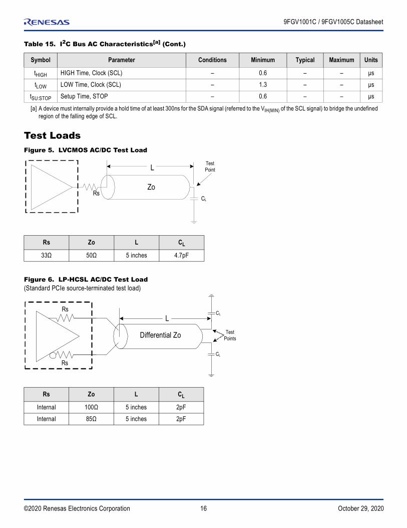
Test LoadsFigure 5. LVCMOS AC/DC Test Load
Figure 6. LP-HCSL AC/DC Test Load(Standard PCIe source-terminated test load)
tHIGH HIGH Time, Clock (SCL) – 0.6 – – μs
tLOW LOW Time, Clock (SCL) – 1.3 – – μs
tSU:STOP Setup Time, STOP – 0.6 – – μs
[a] A device must internally provide a hold time of at least 300ns for the SDA signal (referred to the VIH(MIN) of the SCL signal) to bridge the undefined region of the falling edge of SCL.
Rs Zo L CL
33Ω 50Ω 5 inches 4.7pF
Rs Zo L CL
Internal 100Ω 5 inches 2pF
Internal 85Ω 5 inches 2pF
Table 15. I2C Bus AC Characteristics[a] (Cont.)
Symbol Parameter Conditions Minimum Typical Maximum Units
RsCL
Zo
LTest Point
Rs
RsCL
Differential Zo
CL
Test Points
L
17©2020 Renesas Electronics Corporation October 29, 2020
9FGV1001C / 9FGV1005C Datasheet
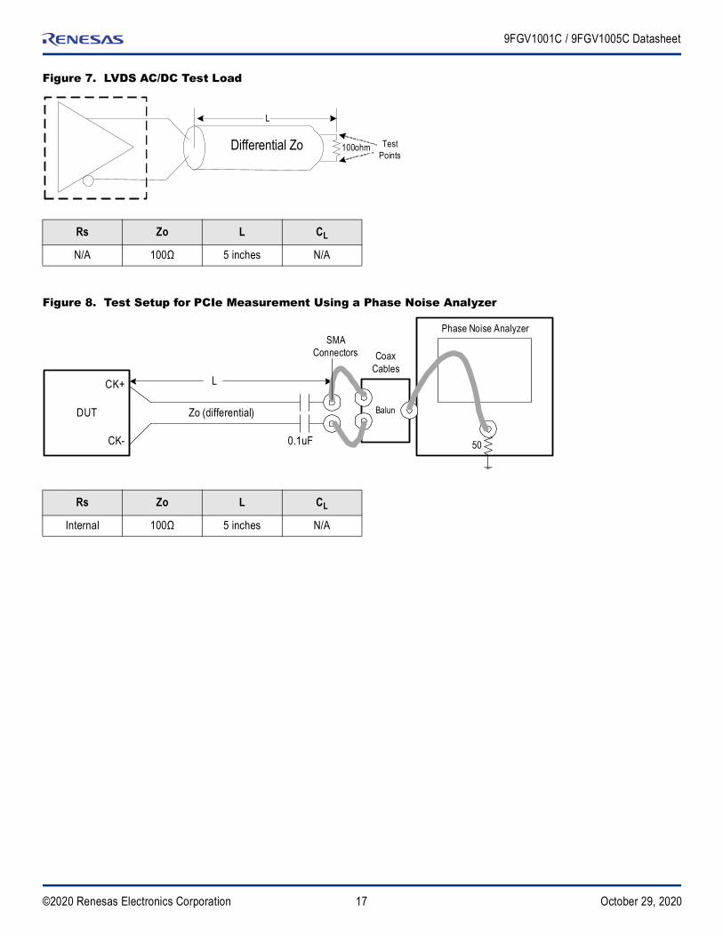
Figure 7. LVDS AC/DC Test Load
Figure 8. Test Setup for PCIe Measurement Using a Phase Noise Analyzer
Rs Zo L CL
N/A 100Ω 5 inches N/A
Rs Zo L CL
Internal 100Ω 5 inches N/A
Differential Zo 100ohm Test Points
L
Phase Noise AnalyzerSMA
Connectors
L
50
CoaxCables
0.1uF
Balun
CK+
DUT
CK-
Zo (differential)
18©2020 Renesas Electronics Corporation October 29, 2020
9FGV1001C / 9FGV1005C Datasheet
Crystal Characteristics
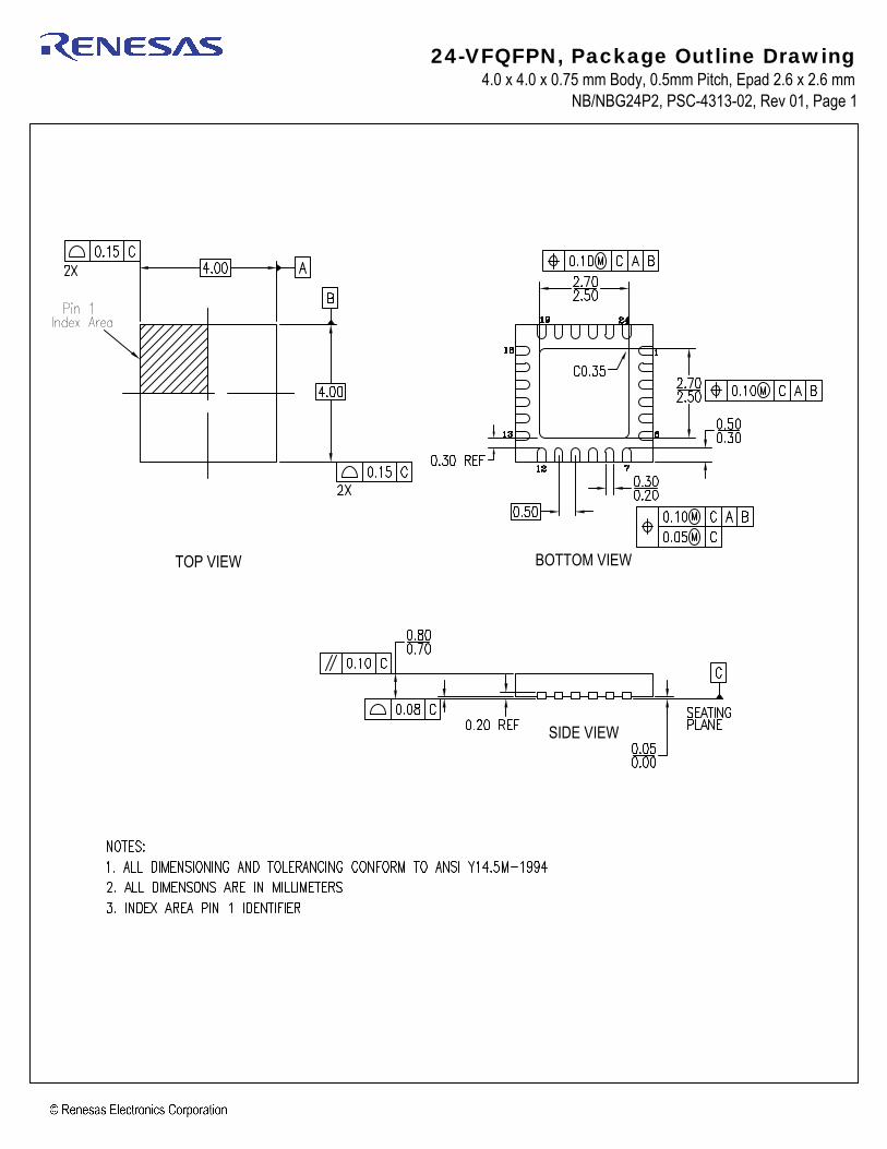
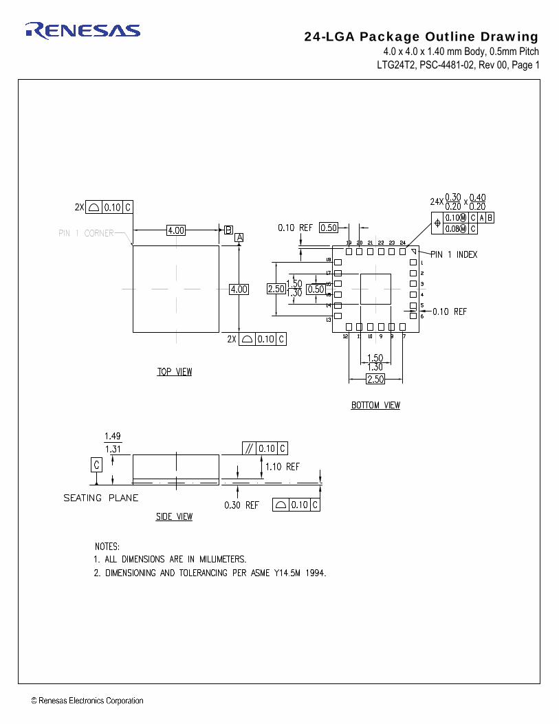
Package Outline DrawingsAre accessible from the links below. The package information is the most current data available and is subject to change without notice or revision of this document.
9FGV1001C:
www.idt.com/document/psc/24-vfqfpn-package-outline-drawing-40-x-40-x-075-mm-body-05mm-pitch-epad-26-x-26-mm-nbnbg24p2
www.idt.com/document/psc/24-lga-package-outline-drawing-40-x-40-x-140-mm-body-05mm-pitch-ltg24t2
9FGV1005C:
www.idt.com/document/psc/16-lga-package-outline-drawing-30-x-30-x-110-mm-body-05mm-pitch-ltg16p1
Table 16. Recommended Crystal Characteristics
Parameter Value Units
Frequency 8–50 MHz
Resonance Mode Fundamental –
Frequency Tolerance at 25°C ±20 ppm maximum
Frequency Stability, REF at 25°C Over Operating Temperature Range ±20 ppm maximum
Temperature Range (commercial) 0–70 °C
Temperature Range (industrial) -40 to 85 °C
Equivalent Series Resistance (ESR) 50 Ω maximum
Shunt Capacitance (CO) 7 pF maximum
Load Capacitance (CL) 8 pF maximum
Drive Level 0.1 mW maximum
Aging Per Year ±5 ppm maximum
19©2020 Renesas Electronics Corporation October 29, 2020
9FGV1001C / 9FGV1005C Datasheet
Thermal CharacteristicsTable 17. Thermal Resistance [a]
[a] EPAD soldered to board.
Parameter Symbol Conditions Package Typical Values Units
Thermal Resistance(devices with external crystal)
θJC Junction to case.
NBG24
52
°C/W
θJb Junction to base. 2.3
θJA0 Junction to air, still air. 44
θJA1 Junction to air, 1 m/s air flow. 37
θJA3 Junction to air, 3 m/s air flow. 33
θJA5 Junction to air, 5 m/s air flow. 32
θJC Junction to case.
LTG16
66
θJb Junction to base. 5.1
θJA0 Junction to air, still air. 63
θJA1 Junction to air, 1 m/s air flow. 56
θJA3 Junction to air, 3 m/s air flow. 51
θJA5 Junction to air, 5 m/s air flow. 49
Thermal Resistance Q-series (devices with internal crystal)
θJC Junction to case.
LTG24
57.3
θJb Junction to base. 24.3
θJA0 Junction to air, still air. 79.8
θJA1 Junction to air, 1 m/s air flow. 73.9
θJA3 Junction to air, 3 m/s air flow. 69.9
θJA5 Junction to air, 5 m/s air flow. 67.3
θJC Junction to case.
LTG16
82.1
θJb Junction to base. 42.3
θJA0 Junction to air, still air. 93.6
θJA1 Junction to air, 1 m/s air flow. 87.1
θJA3 Junction to air, 3 m/s air flow. 83.3
20©2020 Renesas Electronics Corporation October 29, 2020
9FGV1001C / 9FGV1005C Datasheet
Marking DiagramsFigure 9. 9FGV1001C Marking Diagrams
Figure 10. 9FGV1005C Marking Diagrams
Standard ConfigurationsTable 18. 9FGV1001C / 9FGV1005C Standard Configurations
Supply Voltage–all pins (V)
Output Impedance (ohms)
Number of PCIe Clock Outputs
XTAL Frequency (MHz)
Orderable Part Number (Bulk)
Orderable Part Number (Tape and Reel)
3.3 100
425 – external 9FGV1001C001NBGI 9FGV1001C001NBGI8
50 – internal 9FGV1001CQ505LTGI 9FGV1001CQ505LTGI8
225 – external 9FGV1005C001LTGI 9FGV1005C001LTGI8
50 – internal 9FGV1005CQ505LTGI 9FGV1005CQ505LTGI8
1.8 100
425 – external 9FGV1001C002NBGI 9FGV1001C002NBGI8
50 – internal 9FGV1001CQ506LTGI 9FGV1001CQ506LTGI8
225 – external 9FGV1005C002LTGI 9FGV1005C002LTGI8
50 – internal 9FGV1005CQ506LTGI 9FGV1005CQ506LTGI8
Table 19. Common Features of 9FGV1001C / 9FGV1005C Standard Configurations
These common features are collaborative with Table 18.
Configuration Output Frequency (MHz) Output Type Ref Outputs
0 50
LP-HCSL OFF1 100
2 125
3 156.25
▪ Lines 1 and 2: truncated part number:• “nnn” denotes the decimal digits indicating a specific configuration.• “aa” denotes the alphanumeric digits indicating a specific Q5 configuration.
▪ Line 3: • “#” denotes the stepping number.• “YWW” denotes the last digits of the year and week the part was assembled.• “**” denotes the lot sequence; “$” denotes the mark code.
9FGV1001CnnnGI#YWW**$
1001CQ5aaIYWW**$
▪ Line 1: truncated part number• “nnn” denotes the decimal digits indicating a specific configuration.• “aa” denotes the alphanumeric digits indicating a specific Q5 configuration.
▪ Line 2: “YWW” denotes the last digits of the year and week the part was assembled; “$” denotes mark code.
▪ Line 3: “XXX” denotes the last three characters of the lot number.
5CnnnYWW$XXX
5CQ5aaYWW$XXX

21©2020 Renesas Electronics Corporation October 29, 2020
9FGV1001C / 9FGV1005C Datasheet
Ordering Information
“G” indicates RoHS 6.6 compliance.“nnn” are decimal digits indicating a specific configuration.“aa” are alphanumeric digits indicating a specific configuration.“Q5” indicates internal 50MHz crystal.
Table 20. 9FGV1001C / 9FGV1005C Standard Configurations (with 39.0625MHz crystal frequency)
Supply Voltage–all pins
(V)Output Impedance
(ohms)Number of PCIe Clock Outputs
XTAL Frequency (MHz)
Orderable Part Number (Bulk)
Orderable Part Number (Tape and Reel)
3.3 1004 39.0625 – external 9FGV1001C011NBGI 9FGV1001C011NBGI8
2 39.0625 – external 9FGV1005C011LTGI 9FGV1005C011LTGI8
1.8 1004 39.0625 – external 9FGV1001C012NBGI 9FGV1001C012NBGI8
2 39.0625 – external 9FGV1005C012LTGI 9FGV1005C012LTGI8
Table 21. Common Features of 9FGV1001C / 9FGV1005C Standard Configurations (with 39.0625MHz crystal frequency)
These common features are collaborative with Table 20.
Configuration Output Frequency (MHz) Output Type Ref Outputs
0 156.25
LP-HCSL OFF1 161.1328125
2 312.5
3 322.265625
Orderable Part Number Package Carrier Type Temperature Crystal
9FGV1001CnnnNBGI4 × 4 mm, 0.5mm pitch 24-VFQFPN
Tray
-40 to +85°C
External9FGV1001CnnnNBGI8 Tape and Reel
9FGV1001CQ5aaLTGI4 × 4 mm, 0.5mm pitch 24-LGA
Tray50MHz Internal
9FGV1001CQ5aaLTGI8 Tape and Reel
9FGV1005CnnnLTGI
3 × 3 mm, 0.5mm pitch 16-LGA
TrayExternal
9FGV1005CnnnLTGI8 Tape and Reel
9FGV1005CQ5aaLTGI Tray50MHz Internal
9FGV1005CQ5aaLTGI8 Tape and Reel
22©2020 Renesas Electronics Corporation October 29, 2020
9FGV1001C / 9FGV1005C Datasheet
Revision History
Revision Date Description of Change
October 29, 2020 Updated pin descriptions for VDDAp and VDDDp.
September 28, 2020 Added Standard Configurations section and tables.
September 18, 2020 Corrected typo in Features section from 3 x 3 mm 16-LGA (9FGV1006) to 3 x 3 mm 16-LGA (9FGV1005).
August 18, 2020 Updated 9FGV1005CQ marking diagram.
August 14, 2020 Updated Slew Rate 1.8V minimum value from 0.8 to 1.0V/ns.
August 13, 2020 Updated Carrier Type in Ordering Information table from “Cut-Tape” to “Tray”.
July 21, 2020
▪ Merge 9FGV1001 and 9FGV1005 into single data sheet.▪ Update to device Rev C, SEL0 and SEL1 lines now have internal pull-down resistors.▪ Add PCIe Gen5 performance specifications.▪ Updated electrical tables to latest format.
BOTTOM VIEW
SIDE VIEW
TOP VIEW
© Integrated Device Technology, Inc.
24-VFQFPN, Package Outline Drawing
4.0 x 4.0 x 0.75 mm Body, 0.5mm Pitch, Epad 2.6 x 2.6 mmNB/NBG24P2, PSC-4313-02, Rev 01, Page 1
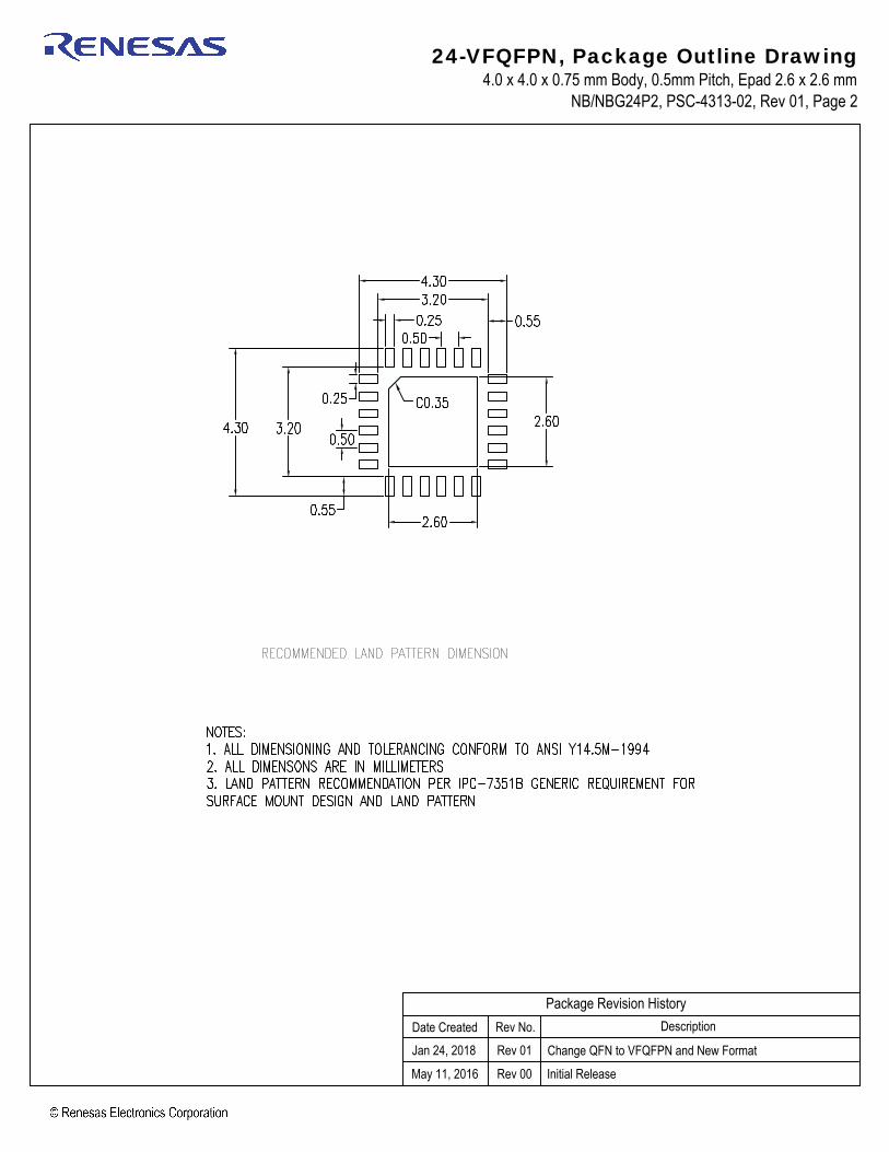
© Integrated Device Technology, Inc.
24-VFQFPN, Package Outline Drawing
4.0 x 4.0 x 0.75 mm Body, 0.5mm Pitch, Epad 2.6 x 2.6 mmNB/NBG24P2, PSC-4313-02, Rev 01, Page 2
Package Revision HistoryRev No.Date Created Description
May 11, 2016 Rev 00 Initial Release
Jan 24, 2018 Rev 01 Change QFN to VFQFPN and New Format
© Integrated Device Technology, Inc.
24-LGA Package Outline Drawing
4.0 x 4.0 x 1.40 mm Body, 0.5mm PitchLTG24T2, PSC-4481-02, Rev 00, Page 1
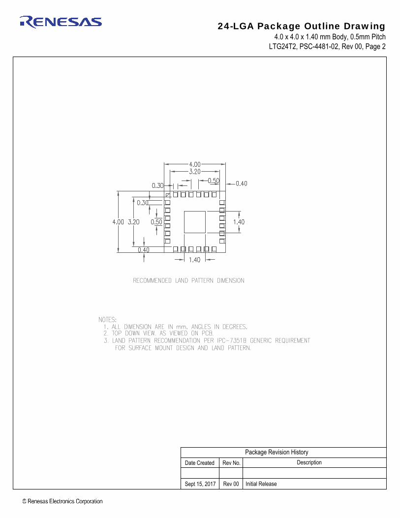
© Integrated Device Technology, Inc.
24-LGA Package Outline Drawing
4.0 x 4.0 x 1.40 mm Body, 0.5mm PitchLTG24T2, PSC-4481-02, Rev 00, Page 2
Package Revision HistoryRev No.Date Created Description
Sept 15, 2017 Rev 00 Initial Release
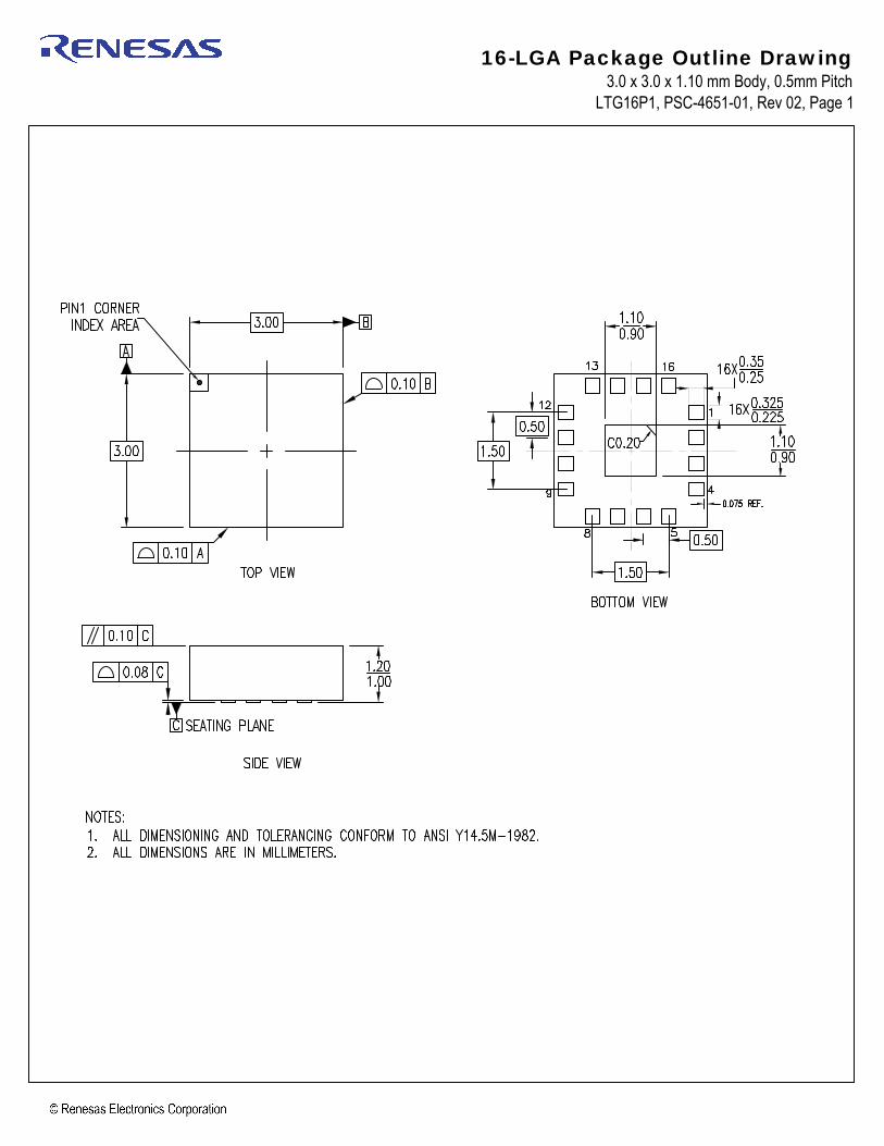
© Integrated Device Technology, Inc.
16-LGA Package Outline Drawing
3.0 x 3.0 x 1.10 mm Body, 0.5mm PitchLTG16P1, PSC-4651-01, Rev 02, Page 1
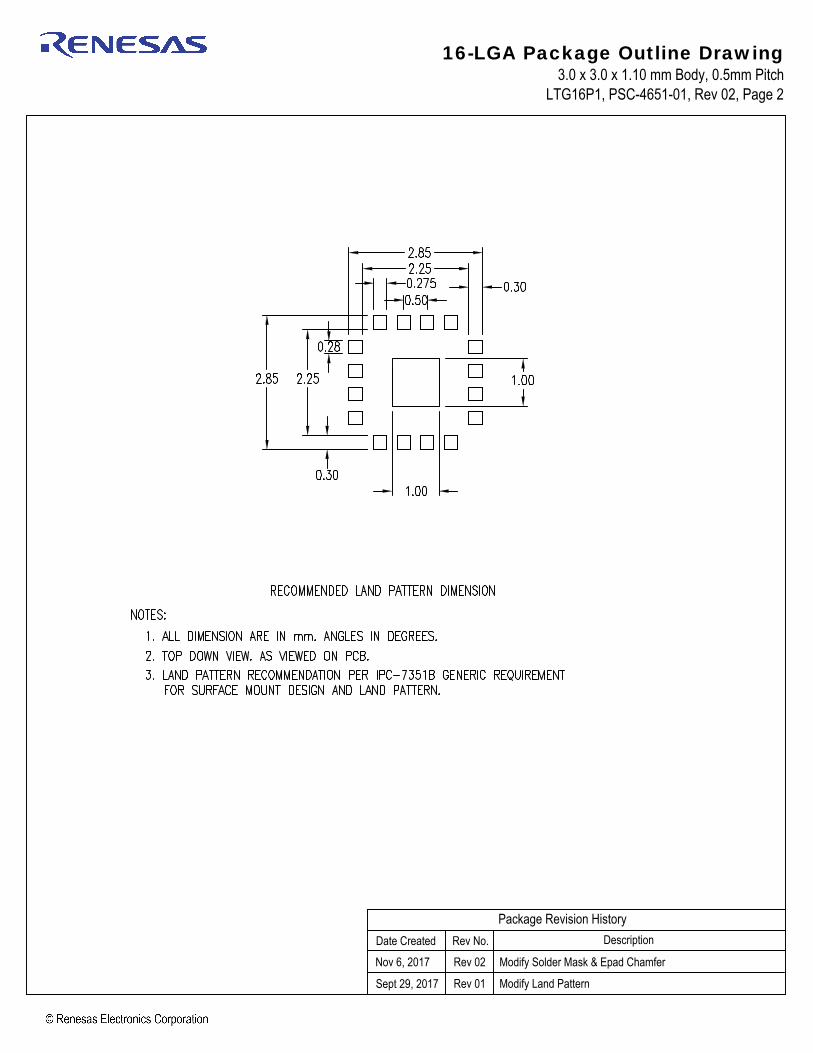
© Integrated Device Technology, Inc.
16-LGA Package Outline Drawing
3.0 x 3.0 x 1.10 mm Body, 0.5mm PitchLTG16P1, PSC-4651-01, Rev 02, Page 2
Package Revision HistoryRev No.Date Created Description
Nov 6, 2017 Rev 02 Modify Solder Mask & Epad Chamfer
Sept 29, 2017 Rev 01 Modify Land Pattern
Corporate HeadquartersTOYOSU FORESIA, 3-2-24 Toyosu,Koto-ku, Tokyo 135-0061, Japanwww.renesas.com
Contact InformationFor further information on a product, technology, the most up-to-date version of a document, or your nearest sales office, please visit:www.renesas.com/contact/
TrademarksRenesas and the Renesas logo are trademarks of Renesas Electronics Corporation. All trademarks and registered trademarks are the property of their respective owners.
IMPORTANT NOTICE AND DISCLAIMER
RENESAS ELECTRONICS CORPORATION AND ITS SUBSIDIARIES (“RENESAS”) PROVIDES TECHNICAL SPECIFICATIONS AND RELIABILITY DATA (INCLUDING DATASHEETS), DESIGN RESOURCES (INCLUDING REFERENCE DESIGNS), APPLICATION OR OTHER DESIGN ADVICE, WEB TOOLS, SAFETY INFORMATION, AND OTHER RESOURCES “AS IS” AND WITH ALL FAULTS, AND DISCLAIMS ALL WARRANTIES, EXPRESS OR IMPLIED, INCLUDING, WITHOUT LIMITATION, ANY IMPLIED WARRANTIES OF MERCHANTABILITY, FITNESS FOR A PARTICULAR PURPOSE, OR NON-INFRINGEMENT OF THIRD PARTY INTELLECTUAL PROPERTY RIGHTS.
These resources are intended for developers skilled in the art designing with Renesas products. You are solely responsible for (1) selecting the appropriate products for your application, (2) designing, validating, and testing your application, and (3) ensuring your application meets applicable standards, and any other safety, security, or other requirements. These resources are subject to change without notice. Renesas grants you permission to use these resources only for development of an application that uses Renesas products. Other reproduction or use of these resources is strictly prohibited. No license is granted to any other Renesas intellectual property or to any third party intellectual property. Renesas disclaims responsibility for, and you will fully indemnify Renesas and its representatives against, any claims, damages, costs, losses, or liabilities arising out of your use of these resources. Renesas' products are provided only subject to Renesas' Terms and Conditions of Sale or other applicable terms agreed to in writing. No use of any Renesas resources expands or otherwise alters any applicable warranties or warranty disclaimers for these products.
(Rev.1.0 Mar 2020)
© 2020 Renesas Electronics Corporation. All rights reserved.