copyright warning &...
TRANSCRIPT
Copyright Warning & Restrictions
The copyright law of the United States (Title 17, United States Code) governs the making of photocopies or other
reproductions of copyrighted material.
Under certain conditions specified in the law, libraries and archives are authorized to furnish a photocopy or other
reproduction. One of these specified conditions is that the photocopy or reproduction is not to be “used for any
purpose other than private study, scholarship, or research.” If a, user makes a request for, or later uses, a photocopy or reproduction for purposes in excess of “fair use” that user
may be liable for copyright infringement,
This institution reserves the right to refuse to accept a copying order if, in its judgment, fulfillment of the order
would involve violation of copyright law.
Please Note: The author retains the copyright while the New Jersey Institute of Technology reserves the right to
distribute this thesis or dissertation
Printing note: If you do not wish to print this page, then select “Pages from: first page # to: last page #” on the print dialog screen

The Van Houten library has removed some of the personal information and all signatures from the approval page and biographical sketches of theses and dissertations in order to protect the identity of NJIT graduates and faculty.
RELIABILITY OF MOS DEVICES - THRESHOLD VOLTAGE INSTABILITY
BY
SESHA RAJAMANI SHANKAR
A DISSERTATION
PRESENTED IN PARTIAL FULFILLMENT OF
THE REQUIREMENTS FOR THE DEGREE
OF
DOCTOR OF SCIENCE IN ELECTRICAL ENGINEERING
AT
NEW JERSEY INSTITUTE OF TECHNOLOGY
This dissertation is to be used only with due regard to the rightsof the author. Bibliographical references may be noted, butpassages must not be copied without permission of the College andwithout credit being given in subsequent written or published work.
Newark, New Jersey1977
VITA
Sesha Rajamani Shankar was born in
He graduated with a
Bachelor of Electrical Engineering degree from Jadavpur
University, India in 1956. He taught undergraduate and
graduate courses in Electrical Engineering at the
Coimbatore Institute of Technology from 1956 to 1958,
and Birla Engineering College from 1958 to 1968 as an
Assistant Professor of Electrical Engineering. He
was also an exchange scholar at the University of
Illinois, where he obtained his M.S. (E.E.) degree in
1960.
While actively working for his Doctorate degree at
N.J.I.T., he was a Graduate Assistant first and later
a part time Instructor in Electrical Engineering and
Mathematics.
Since 1968, he is with Kertron Incorporated, Riviera
Beach, Florida, a manufacturer of power transistors and
is currently Engineering Manager at Kertron.

0 1977
SESHA RAJAMAN I SHANKAR
ALL RIGHTS RESERVED
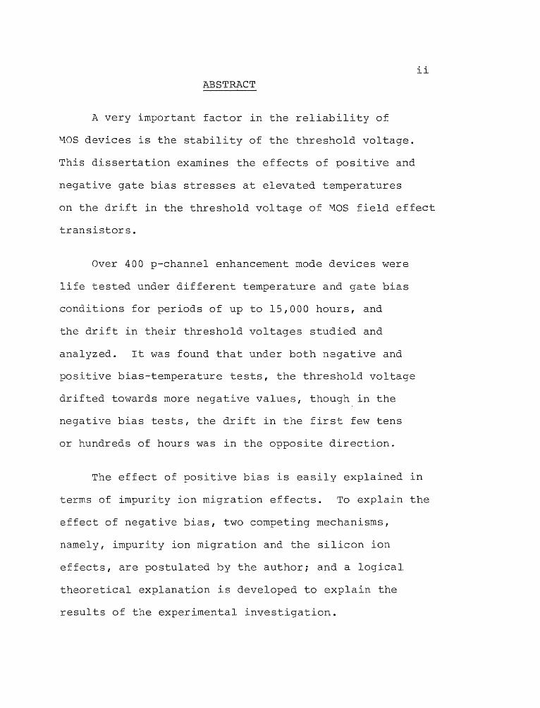
iiABSTRACT
A very important factor in the reliability of
MOS devices is the stability of the threshold voltage.
This dissertation examines the effects of positive and
negative gate bias stresses at elevated temperatures
on the drift in the threshold voltage of MOS field effect
transistors.
Over 400 p-channel enhancement mode devices were
life tested under different temperature and gate bias
conditions for periods of up to 15,000 hours, and
the drift in their threshold voltages studied and
analyzed. It was found that under both negative and
positive bias-temperature tests, the threshold voltage
drifted towards more negative values, though in the
negative bias tests, the drift in the first few tens
or hundreds of hours was in the opposite direction.
The effect of positive bias is easily explained in
terms of impurity ion migration effects. To explain the
effect of negative bias, two competing mechanisms,
namely, impurity ion migration and the silicon ion
effects, are postulated by the author; and a logical
theoretical explanation is developed to explain the
results of the experimental investigation.

APPROVAL OF DISSERTATION
Reliability of MOS Devices-Threshold Voltage instability
By
Sesha Rajamani Shankar
For
Department of Electrical EngineeringNew Jersey Institute of Technology
By
FACULTY COMMITTEE
Approved:
Newark, New Jersey
September, 19 .77

iv
ACKNOWLEDGEMENTS
The author wishes to express his sincere apprecia-
tion and gratitude to his academic advisor, Dr. Raj P.
Misra, for providing objective criticism and encourage-
ment throughout the doctoral program, and to
Dr. Robert E. McMillan, Dr. Mauro H. Zambuto and
Dr. Leon J. Buteau for their helpful comments.
The author also wishes to thank New Jersey Institute
of Technology and the departments of Computer Science,
Mathematics and Electrical Engineering for providing
graduate assistantship and part-time instructorship,
which made this research possible.
Special thanks are due to Mr. William Kearns,
General Manager of Kertron, Incorporated for permitting
the author to take time off for the completion of this
dissertation.

TABLE OF CONTENTS
Chapter Page
I. INTRODUCTION 1
Historical Review 1Oxidation 2The Silicon-Silicon Dioxide System 2Electromigration 7Double-Layer Gate Insulators 7Self-Aligned Gate Electrodes 8Ion Implantation 10Reliability of MOS Devices 11Scope of this Investigation 12
II. BASIC THEORY OF MOSFET's 14
General 14The Mechanism of Conduction in MOSFET's 16Expression for Threshold Voltage 21Importance of Threshold Voltage Stability 24
III. CONSTRUCTION AND RELIABILITY FACTORS 28
Construction 28Reliability Factors 33Gate Protection 36Reliability Assurance Methods 37Failure Modes and Analysis 38
IV. EXPERIMENTAL PROGRAMS AND TEST RESULTS 39
Engineering Definition of Threshold Voltage 39Measurement of Threshold Voltage 39Experimental Program 41High Temperature Life Tests 42High Temperature and NegativeBiasLifeTests 43High Temperature and Positive and NegativeBias Tests 50
V. EXPLANATION OF TEST RESULTS AND PROPOSEDTHEORY ON THE EFFECT OF NEGATIVE BIAS 63
Ionic Contamination of the Oxide 63Effects of Positive Gate Bias and Temp-
erature 64Effects of Negative Gate Bias and Temp-
erature 64
viTABLE OF CONTENTS (continued)
Chapter Page
VI. CONCLUSION AND RECOMMENDATIONS 74
Conclusions 74Recommendations 74
REFERENCES 76
APPENDICES 81
A. Extract of Screening Procedure, MIL-STD-883A,Method 5004.2 81
B. Failure Modes of MOS Devices 83
C. Recommended Sequence of Individual Steps forFailure Analysis 85
D. Summary of Basic Failure Analysis Techniques 86
E. Specifications of ANTI DDO7P, DD07K, DD08P,and DDO8K MOSFETs 91
F. Test Data on All Individual Devices 94
G. Threshold Voltage Definitions 103
BIBLIOGRAPHY 104

viiLIST OF FIGURES
Figure Page
1. P-Channel MOSFET Structure 15
2. Energy Band and Charge Distribution Diagramsfor Different Gate Voltages 17
3. Impurity Ion Charge Density Distribution 23
4. Drain Characteristics of a P-Channel MOSFET 25
5. Thick Oxide Process Steps 30
6. Circuit for Measurement of Threshold Voltage 40
7. Histogram of %age Drift in IVT I of IIIa Units 59
8. Histogram of %age Drift in IVTI of IIIb Units 609. Conditions under Positive Gate Bias & Temp-
erature 65
10. Conditions at VT Measurements (+Ve Gate Biasand Temperature) 66
11. Conditions under Negative Gate Bias and Temp-erature 70
12. Conditions at VT Measurement (-Ve Gate Biasand Temperature) 71

viiiLIST OF TABLES
Table Page
I. Data Summary of High Temperature Life Tests 44
II. Data Summary of High Temperature and NegativeBias Life Tests , 51
III. Data Summary of High Temperature Positive andNegative Bias Tests on DD08K MOSFET 56
IV. Data Summary of High Temperature Negative BiasTests on Additional Category IIIa MOSFETS .61
LIST OF CHARTS
Chart Page
I. Mean of Threshold Voltage - AMI DD07P MOSFETS 46
II. S.D. of Threshold Voltage - AMI DD07P MOSFETS 48
III. Mean and S.D. of VT - AMI DD08P MOSFETS. 53
IV. Mean and S.D. of VT - AMI DD08K MOSFETS 54
V. Mean of VT - Additional DDO8K MOSFETS 62
CHAPTER 1 1
INTRODUCTION
1.1 Historical Review:
An unipolar field-effect transistor was1
described by Shockley in 1952 . Such transistors
were built, tested, and their performance analyzed
by Dacey and Ross 2 . However, the device was only
in the laboratory stage of development, until
advances in semiconductor technology made its
fabrication in the industry feasible 3,4 .
The insulated gate construction was developed
and described by Hof stein, Heiman and others 5,6 .
The high input impedance and fast switching speeds
of these devices made the insulated-gate field-
effect transistor a complement to the bipolar trans-
istor for many applications, and helped in the
complete transistorization of the older electron
tube circuits.
This revival of interest in the field-effect
transistor (FET) in the early sixties led Wallmark 7
to hail its advent as an "Old Device with New Promise".
The theory and performance of the FET have since
been studied and formulated in great depth.8,9,10
Later, Sah and Pao 11 presented a detailed theory,

2summarizing the results of all previous investiga-
tions on the Metal-Oxide-Semiconductor (MOS) FET.
(See also 12 and 13). The further development of
MOS technology led to its easy adoption in the design
and fabrication of the present day integrated
circuits, 14,15,16
1.2 Oxidation:
The gate oxide is an important part of the MOS
structure. The oxidation of silicon is usually
accomplished by thermal growth, which has been
described in detail by Seely and others. 1718
Oxidation at lower temperatures using Si3N4 masks
have been reported on. 19 Oxides have also been
prepared by chemical vapor deposition using SiH 4 -0O2-
H2 sources and have been compared with thermally grown
oxides by Gaind and others.20
The impurities in thermally grown oxide layers
have been analyzed using electron microprobe tech-
niques. 21 Defects such as pinholes in thermal
oxides have been studied 22 . Deal 23 has presented
a concise summary of the nature and properties
of all the charges found in thermally grown oxides.
1.3 The Silicon - Silicon Dioxide System:
The characteristics and operation of a MOS

3device depend heavily on the properties of the
silicon - silicon dioxide interface. A consider -
able amount of study over the years has been devoted
to the properties of the silicon - silicon dioxide
system and to correlate them to the observed
electrical characteristics of MOS devices. 24 These
studies have established the existence of the
following:
a) Fast surface states at the silicon-silicondioxide interface.
b) Fixed positive surface state charge densityat or near the interface.
c) Mobile and fixed ionic charges within thegate oxide.
d) The redistribution of impurities at thesilicon surface during thermal oxidation.
1.3.1. Fast Surface States:
The energy levels of these states fall within
the silicon bandgap. The amount of charge in these
states is a function of the surface potential and
varies with the applied gate voltage. 25 , 26 These
are called "Fast Surface States", because these
charges can easily and quickly be exchanged with
the near-charges of the silicon substrate. The
origin of these states is the disruption of the
periodicity of the silicon lattice near the silicon-
silicon dioxide interface. It has also been found27
4
that the density of fast surface states is
the highest for (111) oriented silicon, and
the lowest for (100) oriented silicon, with
all other process conditions remaining the same.
These fast states act as scattering centers
at the silicon - silicon dioxide interface and
tend to reduce the effective carrier mobility in
the channel. This also results in increasing
the threshold voltage of the device. Castro and
Deal 28 showed that annealing at low temperatures
in an inert or reducing atmosphere (such as hydro-
gen or forming gas) reduces the density of these
states.
1.3.2. Fixed Positive Surface Charge Density, QSS:
This surface state charge in the silicon -
silicon dioxide interface was identified and
studied by Zaininger and others 29,30 . The energy
levels associated with these charges lie outside
the silicon bandgap. Unlike the fast surface
states, these charges are not dependent on the
surface potential or the applied gate voltage. But
the density is highest for (111) oriented silicon
and lowest for (100)orientation. Measurement of
QSS values has been made by using low frequency

5
capacitance-voltage methods 31 and conductance
techniques 32 . The effects of processing on
the value of QSS have been studied. The effects
on Qss of oxidation temperatures and ambients
have been presented by Deal and others 33,34 . The
QSS values could be reproducibly reduced by
annealing in a dry inert gas or in dry oxygen at
an appropriate temperature.
1.3.3. Mobile and Fixed Ionic Charges:
Impurity ions of alkaline metals like sodium
and those of hydrogen, all electropositive in
nature, are known to be present in the oxide
layer 35 . A radiochemical analysis technique of
determining the distribution of sodium ions
was described by Yon36 . These ions are mobile
in the oxide and they diffuse as well as migrate
under temperature and electric field stresses 37 .
Snow38 introduced sodium and Lithium into the
oxide and measured their transport as a function
of time, temperature and voltage stress. Other
studies have also been made on these ionic drifts
by Goetzberger, Hofstein and others. 39,40,41,42
Frequent purging of the oxidizing tubes by HC1
gas and dry oxygen and addition of HC1 to the

6
oxidizing atmosphere are known to reduce the
sodium contamination in the oxide. 43 Use of
phosphosilicate glass over the oxide to
getter the sodium ions is well known in the indus-
try 44 .
Ionizing radiation fromY-rays, X-rays and
electron irradiations also affect the MOS devices 45 .
When a positive or a negative bias is applied to
the gate, there is a build-up of a space-charge
region within the silicon dioxide. There is
also an increase in the fast surface-state
density due to these irradiations. These effects
tend to shift the threshold voltage of the device
under positive and negative gate bias and temp-
erature stresses. Al203 is known to be more
resistant to incident radiation as compared to
Si02.
1.3.4. Impurity Redistribution During Thermal Oxidation:
During thermal oxidation at elevated temper-
atures, the different impurities commonly used
to dope silicon tend to redistribute at the
surface of the silicon substrate 46 ' 47 . Boron
tends to be depleted from the silicon surface,
while phosphorus tends to pile up at the silicon

7
surface during oxidation, the concentration being
dependent on the oxidation temperature, and the
depth of redistribution into the silicon being
dependent on the oxidation temperature as well as
time.
1.4. Electromigration:
Revesz 48 has discussed the possible reactions
at the aluminum metal-SiO2 interface, contributing
to metal ions which migrate into the oxide under
the influence of an electric field. This has
been further studied by Berger and others 49,50 . in
detail. A comprehensive survey of the phenomenon
has been published by Black 51 . To obviate this
phenomenon, silicon gates to replace aluminum
gates have been developed 52.
1.5. Double-layer Gate Insulators:
Both silicon nitride and aluminum oxide are
known to be very effective barriers to sodium ion
migration in the presence of high electric fields 53 .
The preparation and properties of silicon nitride
have been investigated in detail 54,55 . In order
to retain the highly desired properties of the
interface between silicon and thermal oxide and
8
at the same time prevent sodium ion migration,
devices have been fabricated 56 using double-
layer gate insulators. Si02 - Si3N4 and
Si02-Al 203 devices have been fabricated by
manufacturers.
An additional advantage of these devices is the
fact that Si3N4 and Al20 3 have much higher
dielectric constants than Si0 2 and for the same
mechanical thickness, these double-layer insulators
will be electrically equivalent to a thinner
layer of Si02. The threshold voltages can be
made lower as required in integrated circuits,
particularly when they are to be interfaced with
bipolar integrated circuits. The properties of
Metal-Nitride-Oxide-Semiconductor (MNOS) devices
have been compared with those of MOS structures
by several researchers. 57 , 58 , 59
1.6. Self-aligned Gate Electrodes:
Conventional Silicon MOSFETs are not capable of
operating at higher frequencies as compared to the
capability of bipolar devices. In enchancement mode
devices, there is no initial channel present with
zero gate voltage and a conducting channel is
formed only when the gate voltage of appropriate
9
polarity is applied. This feature necessitates
the gate electrode to extend completely over the
region between the drain and the source. In
order that a slight misalignment of the gate
electrode does not ruin the device, it is common
practice to allow the gate electrode to overlap
both the source and the drain electrodes. This
overlap, coupled with the thinness of the insulat-
ing layer, gives rise to appreciable parasitic
capacitances between gate and drain and gate and
source. This provides a negative feed-back
effect which increases with frequency. As a result,
at higher frequencies gain drops off considerably,
accounting for the poorer performance mentioned
above.
In order to reduce the gate-to-drain and
gate-to-source parasitic capacitances,"Self-aligned
Gate Electrodes!' have been developed and used. The
most common material used for the self-aligned
gate electrode is polycrystalline silicon 6061
though molybdenum has also been used 62 . The poly-
crystalline silicon is first deposited over the gate
oxide and then p or n type diffusion of the silicon
substrate is done to form the drain and source
regions. During the diffusion, the polycrystalline
10
silicon gate acts as a mask to prevent the
doping of the channel region. In addition,
the silicon gate itself gets heavily doped
to make it highly conductive, so that no metaliza-
tion is required except for contact.
Because of the difference in work function be-
tween aluminum and silicon, the threshold voltage
is lower for these devices. Since the gate is in
place prior to diffusion, tight tolerance is not
required for definition of the gate. In integrated
circuits, this allows a higher packing density
of components. Also, both poly-silicon and
aluminum layers can be used for interconnections
in integrated circuits 63 .
1.7 Ion Implantation:
The development of ion implantation tech-
nology made it possible to control the threshold
voltage of MOS devices with great flexibility".
It is possible to obtain low threshold voltages
with p-channel devices. High energy ion accelera-
tors are used to implant dopant impurities into
the substrate, the source and drain regions, or
the channel region itself to control the threshold
voltage. It has been found 65 that it is possible

11
to shift the threshold voltage of both p-channel
and n-channel devices, by implanting a small concen-
tration of donor or acceptor impurities through
the gate region into the silicon substrate. In
the case of silicon-gate devices, the gate itself
acts as a mask to protect the underlying channel
region from implantation of dopant ions, while
the source and drain regions alone are doped
by implantation 66 .
Ion Implantation and its ramifications have
been studied in detail by several research-
ers. 67,68,69,70
1.8 Reliability of MOS Devices:
The reliability of semiconductor devices has been
stated71 to be a function of the following:
E - Electric Field
S - Surface
P - Package
A- Ambients
T- Temperature and Temperature Gradient
1Z- Special Factors
The reliability factors with particular reference
to MOSFET's and Integrated Circuits, and micro-
12
electronics in general, have been expounded in
. 72,73, 74, 75detail. Improvements in the reliabil-
ity of integrated circuits have been outlined in a
recent paper by Hawkins 76 .
The various modes and failure mechanisms in
MOS devices have been analyzed and presented in
the literature.77,78,79,80 The available techniques
for failure analysis were summarized by Workman 81 .
The use of electron microscopy for failure diag-
nostics 82 has become very extensive. Studies have
been made of the failure modes at the surfaces and
interfaces by Goetzberger and others. 83 , 84 The
reliability factors involved in the aluminum
metalization on the oxide have been identified85
.
The effects of long term storage on reliability
Of MOS devices have been presented 86 and the results
of accelerated life tests on them published. 87,88
1.9. Scope of this Investigation:
This investigation primarily concerns the
threshold voltage of MOS devices and its stability.
Under positive and negative gate biases at elevated
temperatures,the ionic impurities in the oxide
undergo transports and redistribute. This re-

13distribution along with other factors makes the
threshold voltage drift, thereby affecting the
reliability of the device. These effects are studied
in the investigation.
For purposes of this study, several MOS
field-effect-transistors were put under various
positive and negative gate biases and temperatures
and life tested for several thousand hours. The
threshold voltage of the devices were measured
initially and at appropriate intervals, and the
drifts analyzed. Theories have been developed to
logically explain the results obtained.

14CHAPTER II
BASIC THEORY OF MOSFET's
2.1. General:
The following discussion applies for a
p-channel device, and is applicable with necessary
minor modification to an n-channel device as
well. The mechanism of conduction is described
in detail, the threshold voltage VT is defined,
and a mathematical expression for VT is derived.
The importance of the' stability of VT is also
explained.
In a p-channel device shown in figure 1, the
semiconductor bulk material is n-type silicon,
and the mobile charge carriers deep in the bulk are
electrons. The insulating material on the surface
is silicon dioxide. The electrical condition
that characterizes the silicon at the surface* is
said to be accumulation, depletion, or inversion,
according to whether the mobile charge density at
* "The silicon surface is defined as that region of semi-
conductor material encompassing the outermost layer of
structural silicon atoms inward to that position within
the bulk interior where the energy bands become flat"89.
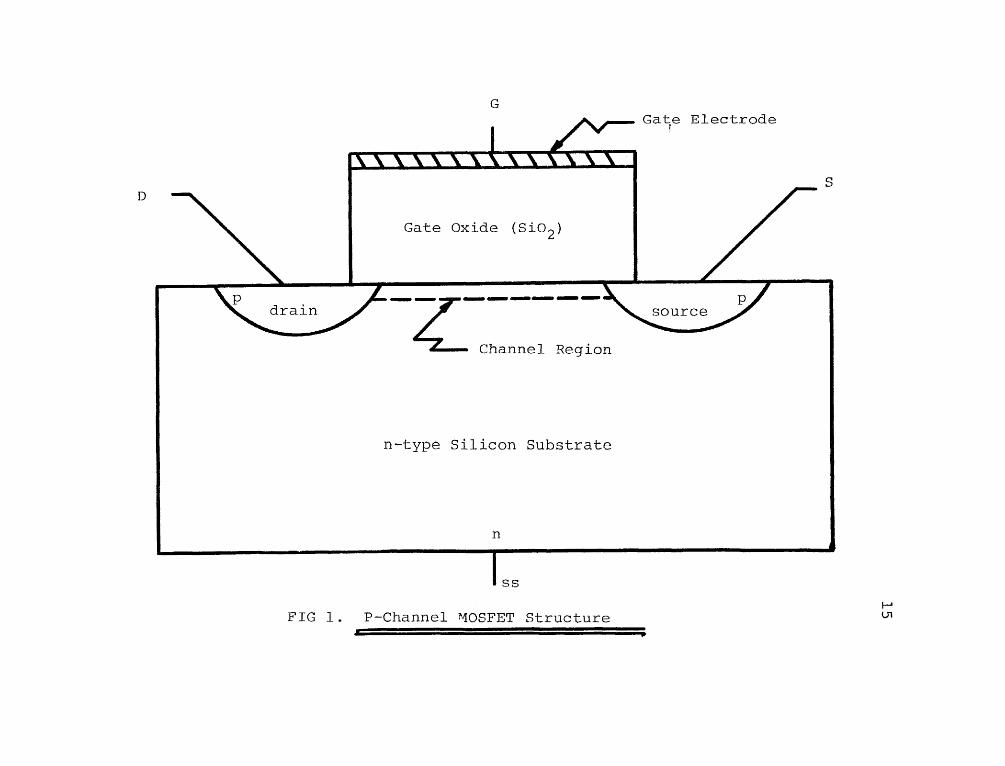
F-'5FIG 1. P-Channel MOSFET Structure •

16
the surface is greater than, less than, or of the
opposite type to that in the bulk silicon.
2.2. The Mechanism of Conduction in MOSFET's:
Figure 2a shows the energy band diagram
of the device with no gate voltage applied. A pos-
itive surface state charge +Q ss always exists in
thermally grown silicon dioxide 90 . Hence electrons
are attracted from within the n-type bulk and
accumulate at the surface. This results in the
downward bending of the conduction and the valence
bands as shown in the figure. In this and the
following diagrams, the intrinsic energy level Ei
is assumed to be midway between the conduction and
the valence bands, while the Fermi level EF is shown
closer to the conduction band, as the material is
of n-type. The Fermi potential is also shown as OF.
The charge density distribution, approximated by
6 functions is shown in figure 2b. The positivesurface charge density +Q ss is balanced by the nega-
tive charge density -QA of the elctrons accumulated
at the silicon surface.
If a negative gate voltage is now applied to
the gate electrode (gate charge = -QG ) such that it
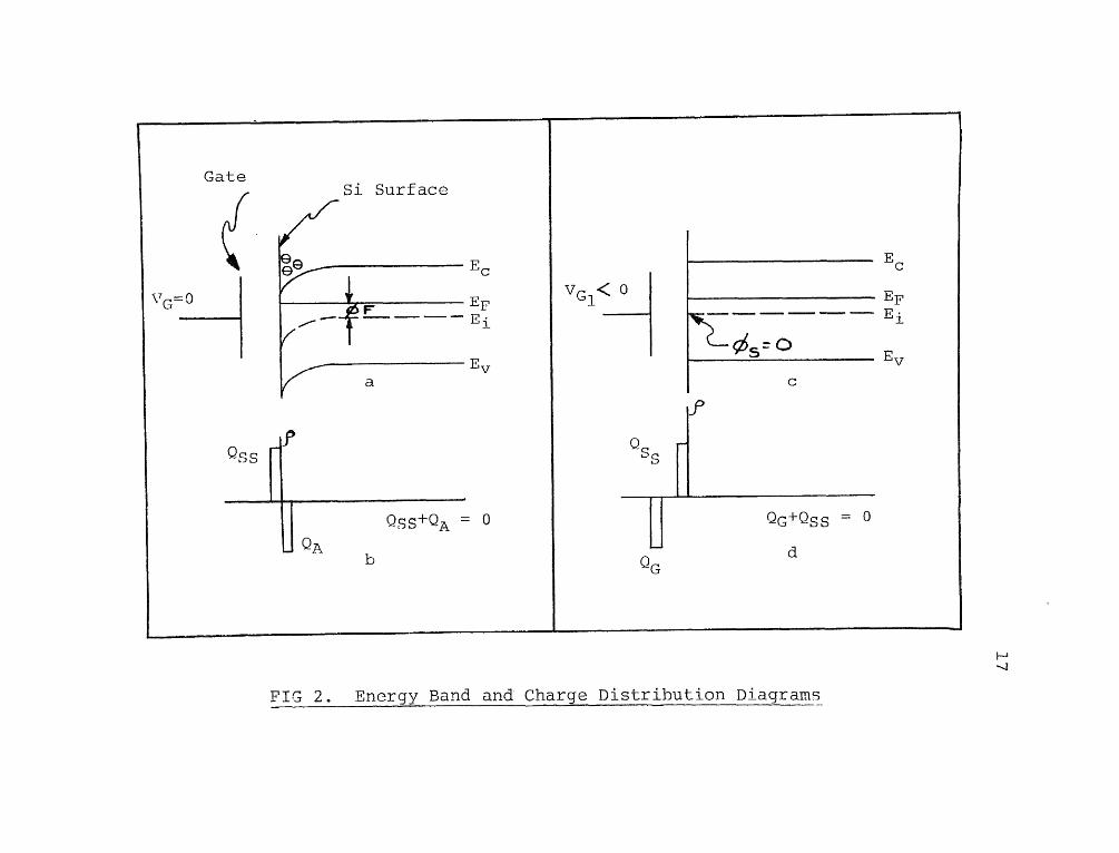
H
FIG 2. Energy Band and Charge Distribution Diagrams
Nco
FIG 2. continued

19
just balances the effect of +Qss , the accumulation
of the electrons near the silicon surface disappears,
and there is no longer any bending of the bands.
The surface potential Os = 0. This condition is
illustrated in figures 2c and 2d, and is known
as the flat band case.
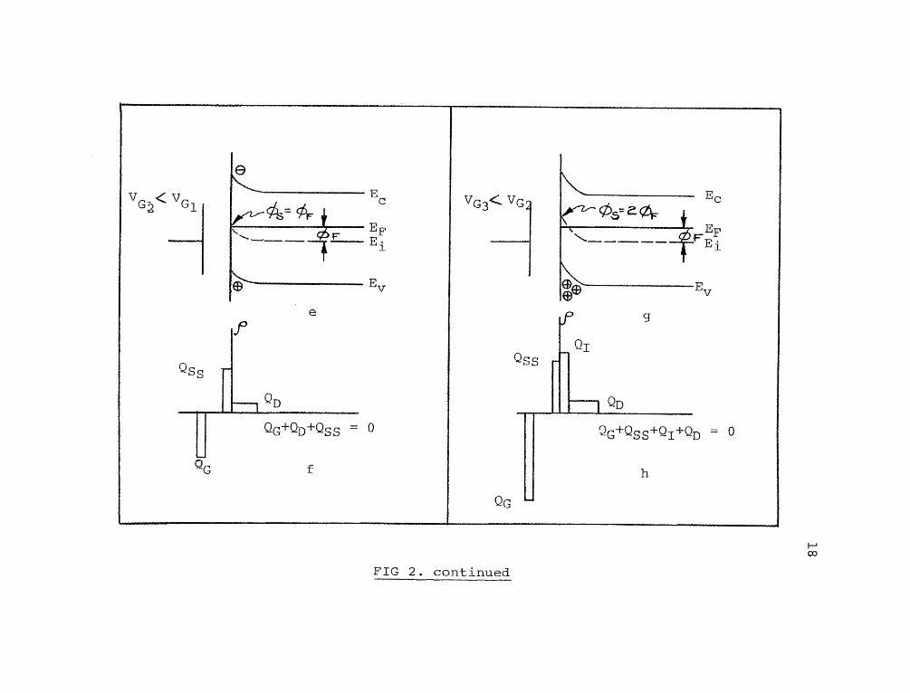
If the negative voltage at the gate is further
increased, the mobile electrons at the donor centers
in the channel region are repelled, and a depletion
region is formed. The charge density +QD in this
depletion region is hence positive. Figures 2e
and 2f depict the energy bands and the charge dis-
tributions respectively under these conditions.
When Ei is bent just sufficiently to intersect
EF at the surface (such that Øs=Ø F) , the surface
has become intrinsic from its initial n-type concen-
tration. In other words, the mobile holes just
equal the mobile electrons at the surface. Under
this condition, the gate charge -Q G must just balance
out the surface state charge +QSS and the depletion
region charge +QD.
When negative gate bias is still further in-
creased, mobile positive holes are attracted towards
the surface, and an increasing percentage of the

20
charge in the channel region is contributed by
holes. At E = EF , mobile electrons still
outnumber holes in the channel region; but as the
gate bias is made more negative, Ei rises above
EF at the surface and the density of holes becomes
more than that of electrons. The surface is now
said to be "inverted". When Ei is sufficiently
greater than EF at the surface to make Øs= 20F,
the surface has become as much p in nature as the
bulk is n. Under these conditions, conduction is
deemed to have commenced between the source and the
drain through the channel. In other words, the
channel region has been inverted and has a positive
charge density +Q 1 . These conditions are shown in
figures 2g and 2h.
The gate voltage at which the conduction thus
commences is called the "Threshold Voltage" of the
device*. Or, the threshold voltage is that voltage
at the gate that produces a gate charge -QG, just
sufficient to counteract the surface state charge
±QSS, and the charge +QD of a depletion region
that supports a potential of 20 F .
* A- practical engineering definition of threshold voltageis given in section 4.1. See also Appendix
21
To summarize, in order to effect conduction in
a p-channel device, a sufficiently negative gate
voltage must be applied so as to produce enough
negative gate charge -QG to
i) counteract +Q SS and undo the accumulation ofelectrons at the surface.
ii) repel mobile electrons from the donor centersin the channel region.
iii) attract into this region sufficient numberof mobile holes, so that the number of holesdominate over the number of electrons. (i.e.)to invert the channel region into a p region.
Finally, it is appropriate to remark that the
onset of conduction is a gradual process of trans-
ition from depletion to inversion, during which there
is a continuous increase of hole concentration in
the channel region, as the electron concentration
simultaneously and continuously decreases.
2.3. Expression for Threshold Voltage:
Based on the discussion in the previous section,
an expression for the threshold voltage can easily
be derived. Let the terms be defined as below:
VT - threshold voltage of the device
QG - charge density on the gate metal
°SS - surface state charge density at thesilicon-silicon dioxide interface
QB - charge density in the bulk
9(x) - impurity ion density at a distance x

22
from the gate electrode (see figure 3)
tox - thickness of the gate oxide
Єox - relative permittivity of silicon dioxide
o - absolute permittivity of vacuum
Øms - work function difference between siliconand the gate metal
The algebraic sum of all the charges in the MOS system
should be zero. The gate oxide region of the MOS
system constitutes in effect a capacitor, charged
by the voltage applied to the gate metal. Under
threshold conditions, the charge on this capacitor
per unit area is
If an additional charge in the oxide contributed by
a distributed impurity ion density (x) as shown
in figure 3 is considered,
Note that the fourth term in the above expression
is obtained by considering the distributed impurity
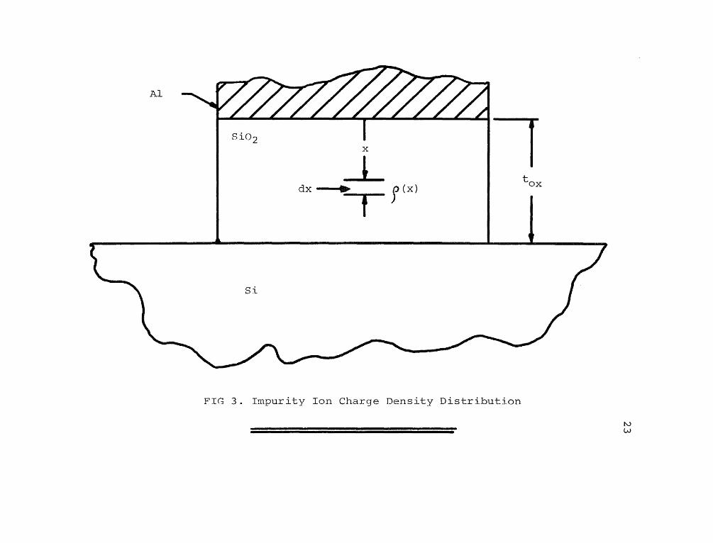
FIG 3. Impurity Ion Charge Density Distribution
24
ion density as an equivalent charge density located
at the gate electrode.
The above equation can now be rearranged and
written conveniently as
Finally, if the gate voltage necessary to counter-
balance the work function difference between the
gate metal and the silicon substrate is also
considered, the expression for the threshold volt-
age stands modified as below:
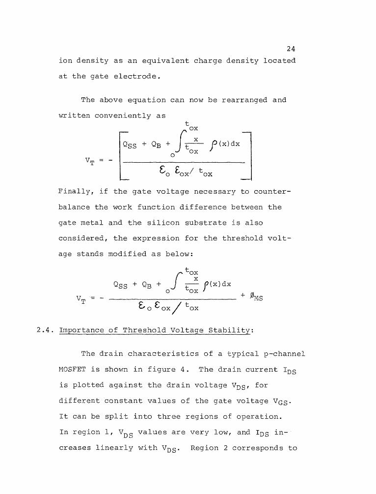
2.4. Importance of Threshold Voltage Stability:
The drain characteristics of a typical p-channel
MOSFET is shown in figure 4. The drain current ' Ds
is plotted against the drain voltage ADS, for
different constant values of the gate voltage VGS.
It can be split into three regions of operation.
In region 1, VDS values are very low, and 'Ds in-
creases linearly with VDS . Region 2 corresponds to
FIG 4. Drain Characteristics of a P-Channel MOSFET
25
26higher values of but saturation has not
commenced. In this region, IDS can be expressed 91
approximately as:
where μp = average mobility of holes in the channel
cox = oxide capacitance
w = width of the channel
1 = length of the channel
In region 3, saturation sets in and I ris is given
by the expresion
In amplifier applications, the load line is so set
to have the operating point well into the saturation
region. The transconductance gm in this region can
be derived as shown below:
From the above expression, it can be seen that any
drift in AT will correspondingly alter gm , thereby
affecting the circuit operation, unless the circuit

27is designed taking this into account.
In switching circuits, the instant of turn-on,
when conduction commences, is directly dependent on
VT . So any drift in VT tends to affect switching
directly.
28CHAPTER III
CONSTRUCTION AND RELIABILITY FACTORS
3.1. Construction:
The discussion here will be confined to the
p-channel device, which is fabricated from a thin
single crystal n-type substrate. Silicon crystal
growth is the first step. The crystal is pulled from
molten silicon containing an appropriate concentra-
tion of a n-type dopant, usually phosphorus. The
crystal orientation commonly used is either (111)
or (100) , and this orientation is identified by
providing a flat in the cylindrical ingot rod. The
rod is then "zone-cut" into different resistivity
ranges. The appropriate resistivity range selected
for the MOSFET fabrication is then sliced into thin
wafers about 8 mils thick, the thickness just suffic-
ient to handle without breakage in subsequent process-
ing. These wafers vary in diameter from an inch to
several inches.
The wafers are then checked for substrate dis-
locations, so as to ensure proper oxide growth in
later processing. They are then lapped and polished
to a high degree, in order that the carrier traps
may be minimized92.

29
The typical "thick oxide" process discussed
hereunder has about 15,000 angstroms thick final
oxide over the diffused p-regions.
The wafers are first thoroughly cleaned before
initial oxidation. They are then placed on a quartz
boat and loaded into the open-ended quartz tube of
an oxidation furnace held at a controlled temperature
(900°C to 1200 °C). An oxide layer of 5000 to 6000angstroms thickness is grown as shown in figure 5a.
This oxide acts as a mask against subsequent
diffusion.
After initial oxidation, comes the first masking
step. Liquid photoresist is spin-coated on the wafer,
which is baked to remove the resist solvents. An
appropriately designed mask is applied and exposed
to a light source. The photo-resist is further
developed by dipping in a suitable solvent. After a
second bake to drive off the residual developer, the
oxide is selectively etched with a solution of hydro-
fluoric acid and ammonium fluoride. The mask pattern
used in this step is to define the source and drain
regions, and to etch off the oxide in those defined
regions (see figure 5b). This operation determines
the critical source-to-drain length, and must be
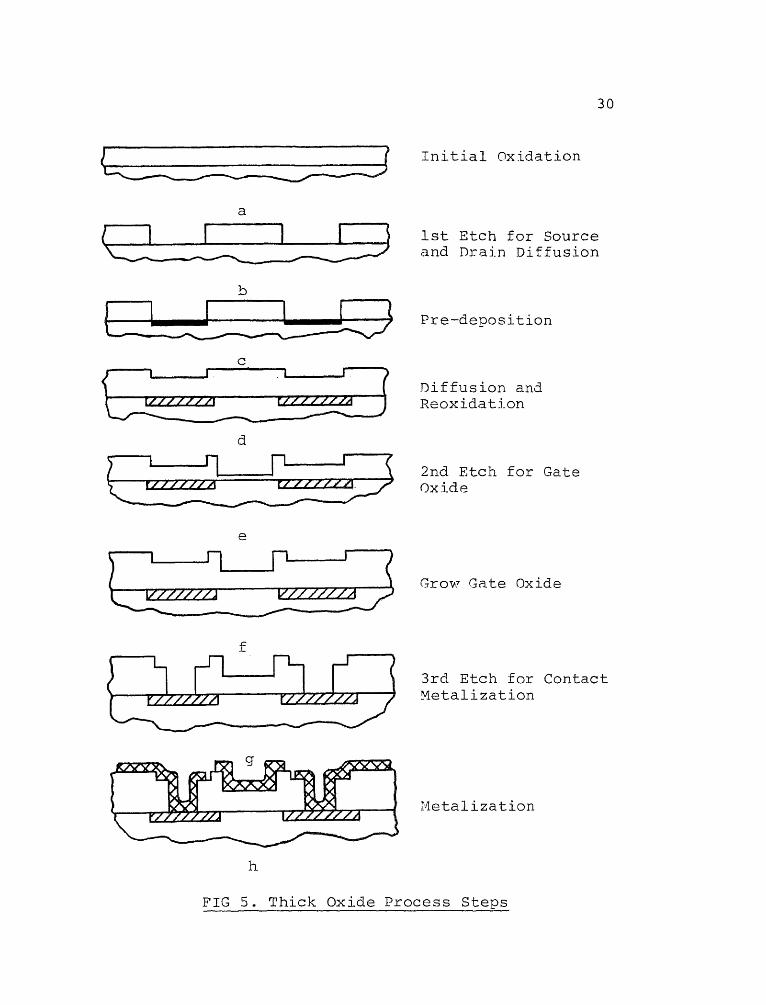
FIG 5. Thick Oxide Process Steps
30

31
tightly controlled.
The next step, namely the p-diffusion of the
source and the drain, is effected in two stages
(figure 5c and 5d). In the first stage, a layer
of the p-type impurity (usually boron) is
deposited on by placing the wafers in a predeposition
furnace tube (at 1000 0C to 1100 °C) using an appropriate
source like diborane (B 2H 6 ) or boron trichloride
(BC13). In the second stage, the wafers are
transfered to a driving furnace, where the p-type
dopant impurity is diffused into the silicon to form
the drain and source regions. A thick oxide layer
of about 15,000 angstroms is again grown over the
surface.
By using a second mask (gate mask), followed
by an etching operation, substantially the entire
thickness of the oxide at the gate region is etched
off as shown in figure 5e. A small amount of over-
lapping of the source and the drain regions by the
gate is designed into this mask. The wafer is now
ready for the gate oxidation, which is done usually
in a dry oxygen atmosphere in an oxidation furnace
at an appropriate temperature. The gate oxide
grown is typically about 1,500 angstroms thick.
This step is shown in figure 5f.
32A third photo-masking and etching step is
performed as shown in figure 5g, in order to remove
the oxide over the drain and source regions, so
that contact metalization can be done. Aluminum
is the most common metalization used. Ultrapure
film of aluminum, 5,000 to 10,000 angstroms
thick, is evaporated on the wafer by using an
evaporator usually of the electron beam type.
This contact metalization is shown in figure 5h.
Finally, the finished wafer is sintered at an
appropriate temperature to ensure proper alloying of
the aluminum with the silicon so as to make the
contact resistance as low as possible.
It can be noted that since (100) oriented
silicon typically gives lower Q ss values as compared
to (111) oriented silicon, lower threshold voltage
values can be obtained with the (100) orientation.
However, as the field oxide threshold voltage is
also correspondingly reduced, compensatory measures
such as increasing the field oxide thickness have
to be taken.
After aluminization, very often the wafers go
through a glass passivation step. A layer of
amorphous SiO2, about 5,000 angstroms thick is vapor
33deposited on top of the aluminum. This is usually
done at 300° to 500°C, temperatures much lower than
the melting point of aluminium, in a resistance heat-
ed reactor using silane (SiH4) and oxygen as the
reactants. Another photomasking and etching oper-
ation is required to remove this oxide from the
bonding pad areas, before the wafers are ready for
assembly.
3.2.Reliability Factors:
Some of the reliability factors involved in the
fabrication of MOS devices are described below:
1. The thick oxide method described in section
3.1 reduces the possibility of pinholes in
the oxide. Apart from the thickness of the
oxide, it can be noted that all areas, except
where the gate overlaps the source and the drain,
the oxide has been grown in two layers. This
minimizes the propagation of pinholes complete-
ly through the oxide.
2. A very high degree of polish in the lapping
operation is essential. Since the MOSFET is a
surface-controlled device, carrier traps should
be reduced to a minimum. This is ensured by
making the surface as evenly flat as possible by
34polishing.
3. Proper alignment of masks used in the photoresist
and etching operations is critically important.
Frequent replacement of photomasks is mandatory.
It is common practice in the industry to replace
masks after 10 to 15 uses.
4. Super clean conditions, particularly in the
photoresist and diffusion areas, are essential.
Dust-free dehumified air flow, use of laminar
flow hoods, use of pure deionized water in the
cleaning operations, use of high purity
"electronic" or "reagent" grade etchant solutions,
and prevention of contamination from extraneous
sources including the operating personnel are very
important.
5. Before the aluminum metalization is done, it is
good practice to etch off 50 to 150 angstroms of
the gate oxide, in order to remove any sodium
contamination due to the photoresist residues.
6. The electron beam evaporater for metalization
is preferred, as it gives cleaner metalization
free from alkaline ion contamination. In order
to ensure uniform thickness of deposited aluminum,
35special fixtures have been designed to
planetarily rotate the wafers, so as to provide
varying angles of incidence between the wafers
and the evaporater source.
7. Where stepping of the oxide is involved under
the metalization, they are appropriately sloped
to ensure that metalization cracks do not develop,
creating a reliability problem due to reduced
crosssection of metalization.
8. Passivation of the wafer surface greatly helps
in eliminating or at least, minimizing the
possibilities of scratches on the metalization, in
addition to reducing surface ion migration. The
presence of a small amount of phosphorus oxide
in the passivating layer acts as a "getter" to
trap and immobilize alkali ions, which contribute
to instability. 93
9. Over-alloying of aluminum into base silicon on the
p-region contact cutouts should be avoided.
Though this alloying is done by sintering at closely
controlled temperatures, further alloying does
occur in several subsequent operations such as
die-attaching, wire-bonding etc., where temperatures
about 400°C are used. The time duration for which
36
the die is exposed to this temperature
during assembly should be minimum, subject
of course to the requirements of good die-
attach and wire-bond. For the same reason,
ultrasonic wire-bonding is preferred to
thermocompression bonding.
10. Freedom from contamination is as important
for the package as it is for the die. The
package bases as well as caps should be effect-
ively cleaned before use in the assembly line.
Between such cleaning and their actual use in the
assembly, they should be stored under clean and
inert conditions.
3.3 Gate Protection:
The fact that the gate of a MOSFET acts as a
capacitor makes the device very sensitive to damage
by stray electrostatic charges, that can be generated
during normal handling. A typically 1500 Angstroms
thick gate oxide would require at most 150 volts
to break down, assuming a high quality oxide with a
breakdown strength of 107 volts/cm. Assuming a gate
capacitance of 4 pf, this voltage would need only a
small charge of (4 x 10 -12 ) (150) Coulomb or 0.6
nCoulomb. Hence protective devices are very often

37
incorporated into the construction of MOS devices.
The most common form of protection is a diffused
diode in parallel with the gate 94 . The breakdown
voltage of this diode is designed to be just above
the maximum operating gate voltage of the device.
Its dynamic resistance in breakdown should also be
low. Another form of protection is the incorporation
of also a diffused resistor in series with the gate,
which helps to limit the current during breakdown 95 .
3.4 Reliability Assurance Methods:
In conjunction with production, it is also import-
ant to provide reliability assurance. Most quality
assurance specifications include references to the
following documents:
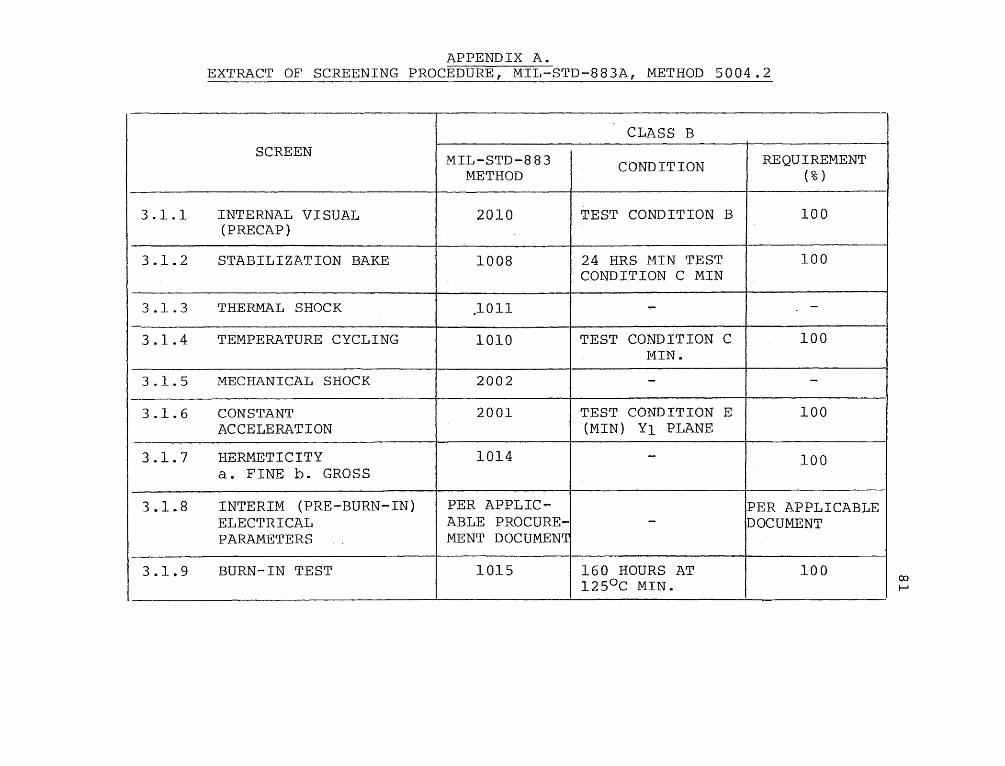
MIL - STD - 883A Test Methods and Procedures forMicroelectronics.
MIL - M - 38510 Microcircuits, General Specifica-tions for.
Uniform methods for testing are established by
MIL - STD - 883A. These tests include environmental,
mechanical, and electrical screening tests. A typical
screening procedure is shown in tabular form in Appendix
A.

38
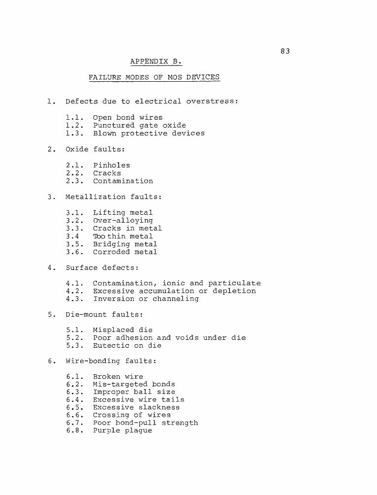
3.5 Failure Modes and Analysis:
Some of the common modes of failure of MOS devices
are listed in Appendix B. These include wafer-
processing and assembly related failures, mechanical
defects, and surface failures.
Failure analysis is a useful tool to discern
from the failed unit the extent of its deterioration
and cause of failure, so that corrective measures to
improve reliability can be instituted based on the
study. The proper sequence of individual tests
is very critical, in order not to destroy evidence.
The recommended sequence of individual steps and
a summary of basic failure analysis techniques are
given in Appendix C and Appendix D respectively.
39CHAPTER IV
EXPERIMENTAL PROGRAMS AND TEST RESULTS
4.1. Engineering Definition of Threshold Voltage:
As explained in chapter II, section 2,2, the
threshold voltage of a p-channel enhancement mode
MOSFET is the gate voltage required for the onset
of conduction from source to drain through the
inverted channel. For practical measurement
purposes howver, engineering practice more specific-
ally defines the threshold voltage (VT) for
p-channel devices as the gate-to-source voltage
(VGS) required to generate a drain-to-source
current (/DS) through the channel of a specified
value, under the condition VDS = VGS (i.e. with
the drain and gate terminals connected together).
The specified IDS value for the devices tested in
this study was -l0uA.
4.2. Measurement of Threshold Voltage:
The circuit used for the measurement of thres-
hold voltage is shown in figure 6. A General Radio
D.C. amplifier and electrometer, type 1230A, was
used for monitoring the drain current, while a
Hewlett Packard A.C. - D.C. differential voltmeter,
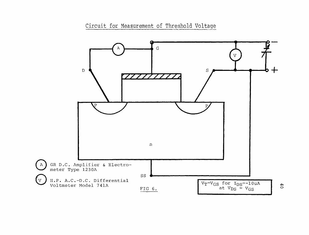
Circuit for Measurement of Threshold Voltage
FIG 6.
41
model 741A, was used to measure the threshold
voltage. The latter instrument enabled the
measurement of VT upto the 4th decimal (0.1 mV).
As already explained in Chapter III,
section 3.3, the inadvertent application of even
a small electrostatic charge to the gate of an
MOS device can cause a large enough voltage
gradient in the gate oxide to damage it. Hence
extreme precautions were taken in handling these
devices, A metal wrist strap connected to a
good ground connection was worn by the operator
while taking measurements. When the devices were
not under test, they were always kept with all
leads connected together to avoid any possible
damage, unless otherwise required.
4.3. Experimental Program:
Several p-channel MOSFETs were put under life
test under different high temperature stresses as
well as temperature and bias stresses for several
thousand hours. The threshold voltages were
measured initially and at appropriate intervals of
time. Their means and standard deviations were
calculated and the drifts in threshold voltage
with time studied and analyzed. Special care was

42taken to ensure the accuracy of measurements.
The several categories of life tests undertaken
and the results obtained therefrom are explained
in the following sections.
The devices used for the tests were DD07P,
DDO8P, and DD08K type MOSFETs, manufactured by
American. Microsystems Inc. These 3 types were of
identical construction and ratings, except that
DD07P had a protective gate zener, absent in the
DD08P and DD08K types. The detailed specifications
of these devices are given in appendix E,
4,4. High Temperature Life Tests:
97 DD07P type devices were used for these tests.
The different storage temperatures and the number
of devices under each condition are listed below:
Category Storage Conditions # of Devices
Ia Temperature of 80° + 3°C 40with all leads tied together
Ib Temperature of 100° + 3 °C 40with all leads tied together
Ic Room temperature (22° + 2 0C) 17with all leads tied together
TOTAL 97

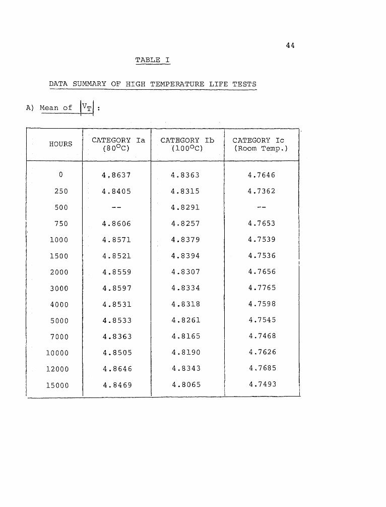
43These life tests were carried out upto
15,000 hours, and VT measurements were taken
at peiodic intervals. A summary of the data
is presented in table I (A & B), and charts I&II.
The drift from 0 hours to 15,000 hours in the
mean value as well as the standard deviation of
the threshold voltage of the units of all these
three categories were well under 1%, and hence
considered insignificant.
4.5. High Temperature and Negative Bias Life Tests;
A second group of 235 devices, consisting of
98 DD08P units and 137 DD08K units, were used
for these tests. The life test conditions and
quantities were as shown below:
Category Storage Conditions # of DevicesDD08P DD08K
IIa
IIb
IIc
Room temperature (22 0+2°C) 20 26with all leads tied together
Temperature of 140 °C+5 °C 40 55with all leads together
Temperature of 140 °C+ 5°CBias VCS = -56V; source, 38 56drain, and substrate tiedtogether
TOTAL 98 137
44
TABLE I
DATA SUMMARY OF HIGH TEMPERATURE LIFE TESTS
A) Mean of |VT| :
HOURS CATEGORY Ia(80°C)
CATEGORY Ib(100°C)
CATEGORY Ic(Room Temp.)
0 4,8637 4.8363 4.7646
250 4.8405 4.8315 4.7362
500 -- 4.8291 --
750 4.8606 4.8257 4.7653
1000 4.8571 4.8379 4.7539
1500 4.8521 4.8394 4.7536
2000 4.8559 4.8307 4.7656
3000 4.8597 4.8334 4.7765
4000 4.8531 4.8318 4.7598
5000 4.8533 4.8261 4.7545
7000 4.8363 4.8165 4.7468
10000 4.8505 4.8190 4.7626
12000 4.8646 4.8343 4,7685
15000 4.8469 4.8065 4.7493

45TABLE I (continued)
B) Standard. Deviation of VT :
HOURSCATEGORY Ia
(80°C)CATEGORY Ib
(100°C)CATEGORY Ic(Room Temp.)
0 0.1530 0.1678 0.2852
250 0.1497 0.1640 0.2785
500 _ _0.1609 --
750 0.1478 0.1612 0.2792
1000 0.1482 0.1599 0.2765
1500 0.1495 0.1602 0.2770
2000 0.1491 0.1595 0.2773
3000 0.1496 0.1628 0.2792
4000 0.1549 0.1625 0.2876
5000 0.1540 0.1647 0.2869
7000 0.1537 0.1632 0.2887
10000 0.1538 0.1630 0.2868
12000 0.1569 0.1627 0.2870
15000 0.1558 0.1638 0.2881

110111-
6Chart Mean of Threshold Voltage - AMI DD07P MOSFET's

fl.Chart I. continued 47
Chart II. S.D. of Threshold Voltage - AMI DDO7P MOSFET's co

Chart II - continued ,4...1)
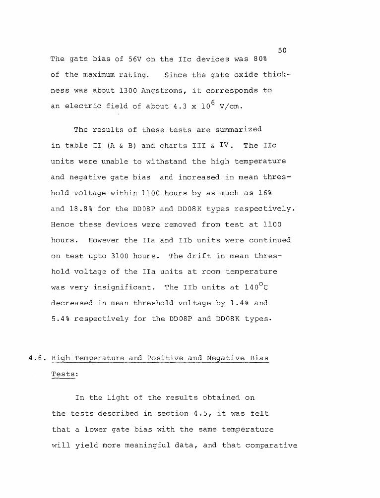
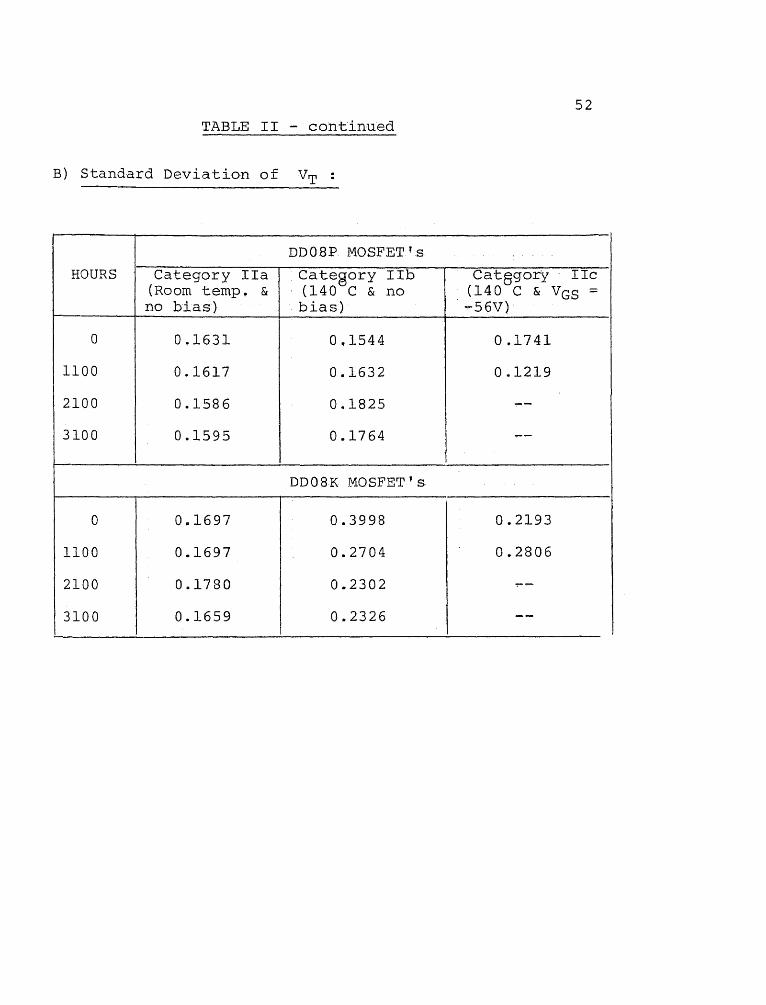
50The gate bias of 56V on the IIc devices was 80%
of the maximum rating. Since the gate oxide thick-
ness was about 1300 Angstroms, it corresponds to
an electric field of about 4.3 x 10 6 V/cm.
The results of these tests are summarized
in table II (A & B) and charts III & IV. The IIc
units were unable to withstand the high temperature
and negative gate bias and increased in mean thres-
hold voltage within 1100 hours by as much as 16%
and 18.8% for the DD08P and DD08K types respectively.
Hence these devices were removed from test at 1100
hours. However the IIa and IIb units were continued
on test upto 3100 hours. The drift in mean thres-
hold voltage of the IIa units at room temperature
was very insignificant. The IIb units at 140 ° C
decreased in mean threshold voltage by 1.4% and
5.4% respectively for the DD08P and DD08K types.
4.6. High Temperature and Positive and Negative Bias
Tests:
In the light of the results obtained on
the tests described in section 4.5, it was felt
that a lower gate bias with the same temperature
will yield more meaningful data, and that comparative

51TABLE II
DATA SUMMARY OF HIGH TEMPERATURE AND NEGATIVE BIAS LIFE
TESTS
A) Mean of I VTI:
HOURS
DD08P MOSFET'sCategory IIa T Category IIb Category IIc(Room temp. & (140°C & no bias) (140°C & VGS = no bias) -56V)
0 4.2755 4.3412 4.2988
1100 4.2695 4.3018 4.9847
2100 4.2928 4.2914 --
3100 4.2846 4.2795 --
1DD08K MOSFET's
0 4.3353 4.4932 4,3957
1100 4.3013 4.3593 5.2215
2100 4.3422 4.2660 --
3100 4.3527 4.2488 --
52
TABLE II - continued
B) Standard Deviation of VT :
HOURS
DD08P MOSFET's
Category IIa Category lib Category IIc(Room temp. & (140 C & no (140 C & VCS =no bias) bias) -56V)
0
1100
2100
3100
0.1631 0.1544 0.1741
0.1617 0.1632 0.1219
0.1586 0.1825
0.1595 0.1764 --
DDO8K MOSFET's
0 0.1697 0.3998 0.2193
1100 0.1697 0.2704 0.2806
2100 0.1780 0.2302
3100 0.1659 0.2326 --
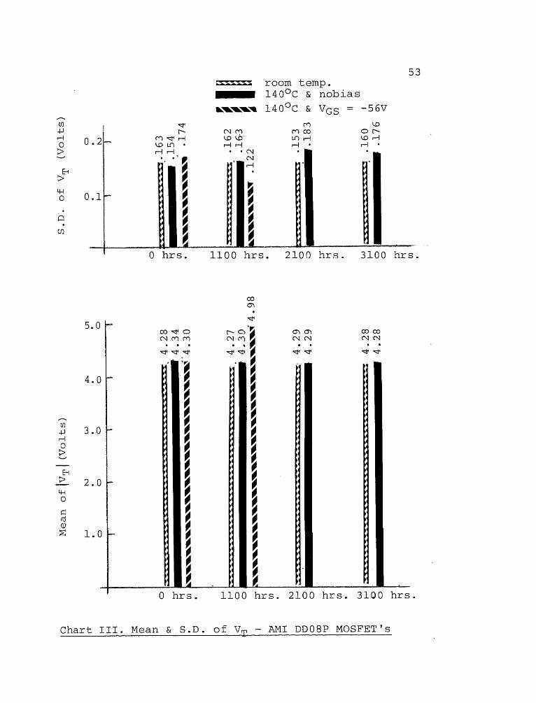
Chart III. Mean & S.D. of VT AMI DD08P MOSFET's
53
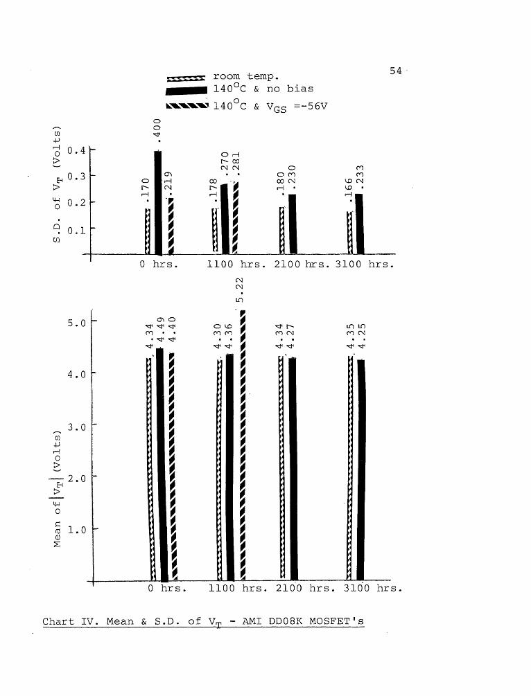
Chart IV. Mean & S.D. of VT AMI DD08K MOSFET's
54
55data on the effect of positive and negative gate
bias will be useful. Hence 47 more devices of the
DD08K type were life-tested under the following
new conditions:
Category Storage Conditions # of Devices
IIIao
Temperature of l40+ 5°C 23and VGS = -28V; source, drain,and substrate tied together
IIIb Temperature of 140 °+5 °C and 24VGS = +28V; source, drain, andsubstrate tied together
Gate bias of 28V was 40% of the maximum rating,
contributing an electric field in the gate oxide
of about 2.15 x 10 6 v/cm.
The data obtained on these devices upto 260
hours is summarized in table III. All the IIIb
units (with positive bias) showed an increasedIV T I
within 260 hours, the increase in meanIV T Ibeing 8.7%.
But, out of the 23 IIIa units (with negative bias),
13 showed an average increase inIVTIof 7.7%, while
the other 10 showed an average decrease of 4.5%.
If all the IIIa units are taken together, mean |V.TI
showed an increase of 2.3%. Histograms on

56
TABLE III
DATA SUMMARY OF HIGH TEMPERATURE POSITIVE AND NEGATIVE
BIAS TESTS ON DD08K MOSFETS:
Mean and Standard Deviation of |VT|
I
CategoryIIIa
(140°C & VGS = -28V)IIIb(140°C & VG S = +28V)
Hours 0 260 0 260
Mean 4.3654 4.4670 4.5265 4.9211
StandardDeviation 0.3996 0.5303 0.3904 0.4355
57the percentage drift in IVT I of these devices
are presented in figures 7 and 8.
11 of the IIIa units were continued on test
upto 1,500 hours. The unit which had shown
increase in FT ' continued to increase upto about
480 hours and then stabilized. But those units which
had shown decrease in IVT I began later to increase
and eventually stabilized within 1,500 hours.
In order to confirm the validity of the above
results, an additional larger sample of 22 DD08K
type devices were tested under category IIIa
conditions (140 °+5°C and VGS
= -28V). Threshold
voltage measurements were taken this time at more
frequent time intervals (0 hours, 46, 75, 120,
195, 390, 580, 840, 1200, and 1500 hours). Except
for 1 unit, all the rest drifted in IV T I to a
lower value at 46 hours. But the IVT I values startedincreasing on all units at least within 390 hours,
and continued to increase beyond 390 hours. The
VT drift eventually stabilized within 1500 hours.
The data summary on these units is presented in Table
IV and Chart V.
The data on all individual units of category
IIIa, IIIb, and the additional IIIa units are pre-
58
sented in appendix F.
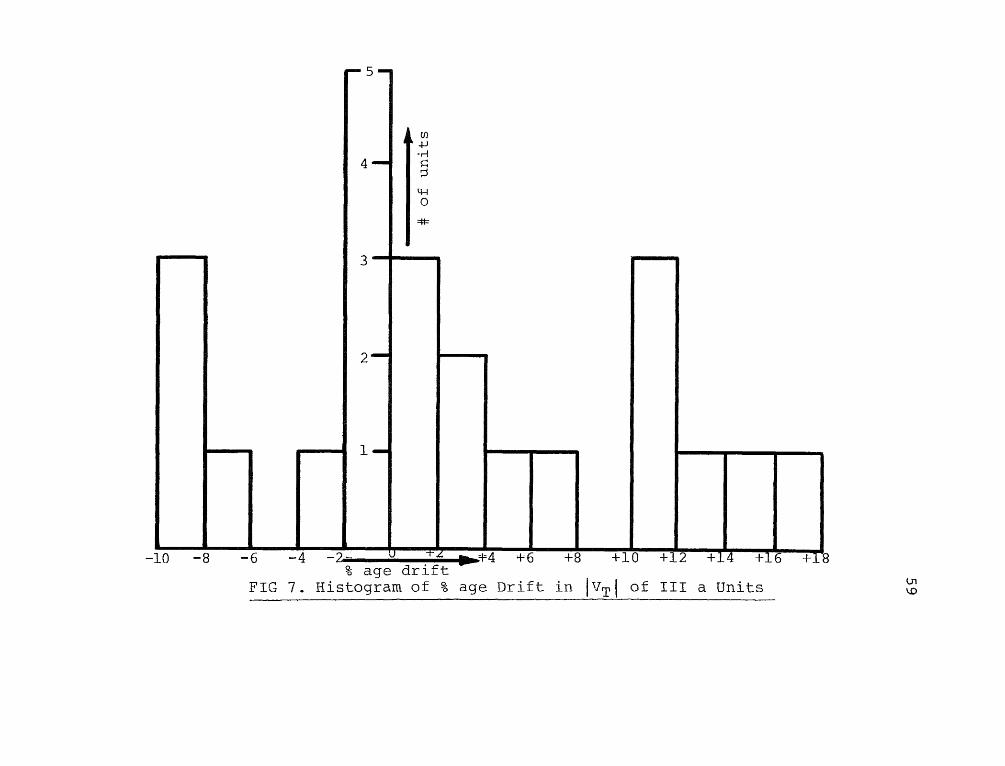
o age driftFIG 7. Histogram of % age Drift in 'VT ' of III a Units

Y5 age drift 6
FIG 8. Histogram of % age Drift in |VT| of IIIb Units
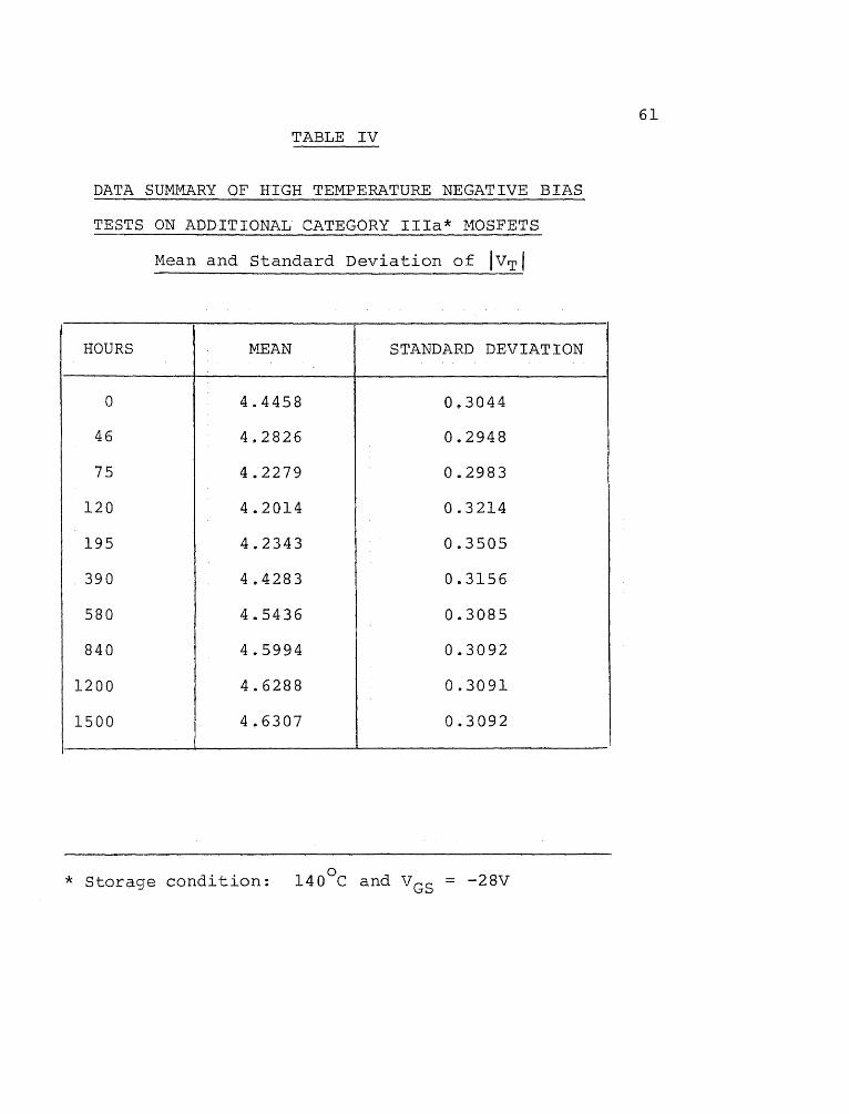
61TABLE IV
DATA SUMMARY OF HIGH TEMPERATURE NEGATIVE BIAS
TESTS ON ADDITIONAL CATEGORY IIIa* MOSFETS
Mean and Standard Deviation of |VT|
HOURS MEAN STANDARD DEVIATION
0 4.4458 0.3044
46 4.2826 0.2948
75 4.2279 0.2983
120 4.2014 0.3214
195 4.2343 0.3505
390 4.4283 0.3156
580 4.5436 0.3085
840 4.5994 0.3092
1200 4.6288 0.3091
1500 4.6307 0.3092
* Storage condition: 140°C and VGS = -28V
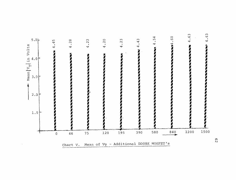
Chart V. Mean of VT - Additional DDO8K MOSFET's
63
CHAPTER V
EXPLANATION OF TEST RESULTS AND PROPOSED
THEORY ON THE EFFECT OF NEGATIVE BIAS
5.1. Ionic Contamination of the Oxide:
As has often been reported 96,97,98 , the gate
oxide layer of a MOSFET has extraneous ionic
impurities, which have been mostly stated to be
those of alkali metals. Sodium can easily get
introduced into the oxide during the manufacturing
process at any process step. Any process material,
solvent or the ambient can act as a source of sodium.
In addition, hydrogen atoms, when ionized, are
electropositive in nature. Under high enough
electric fields, not only ionization, but also
migration of these ions takes place100,101. This
migration however is at a slow rate, and is depend-
ant on temperature as well as size, weight, and
binding energy of the particular ionic impurity
involved. While the hydrogen ions are mobile even
at room temperature, the sodium ions drift occurs at
above 100°C or lower102 . Some negative charges
have been also noted under certain conditions,
but they do not drift at temperatures much below
300°C, as observed by Deal102.
64The results of life tests presented in chapter
IV show that, while high temperature alone do not
cause the threshold voltage to drift very much,
high temperature along with positive or negative
gate bias cause considerable shifts in C T .
5.2. Effects of Positive Gate Bias and Temperature:
Under positive gate bias and elevated
temperature, the elctropositive impurity ions in
the gate oxide tend to migrate towards the oxide-
silicon interface, as shown in figure 9. The
increased positive ionic charge density near the
oxide-silicon interface tends to oppose channel
inversion (see figure), and hence necessitates a
higher applied negative gate voltage to invert
the channel. In other words, the threshold volt-
age of the device becomes more negative. This
can also be seen directly from the expression for
CT given in section 2.3., and is consistent with
the test results obtained on category IIIb units
(140°C & CGS = +28C). Figure 10 shows the condi-tions under VT measurements for this case.
5.3. Effects of Negative Gate Bias and Temperature:
Under negative gate bias of CGS = -56V and
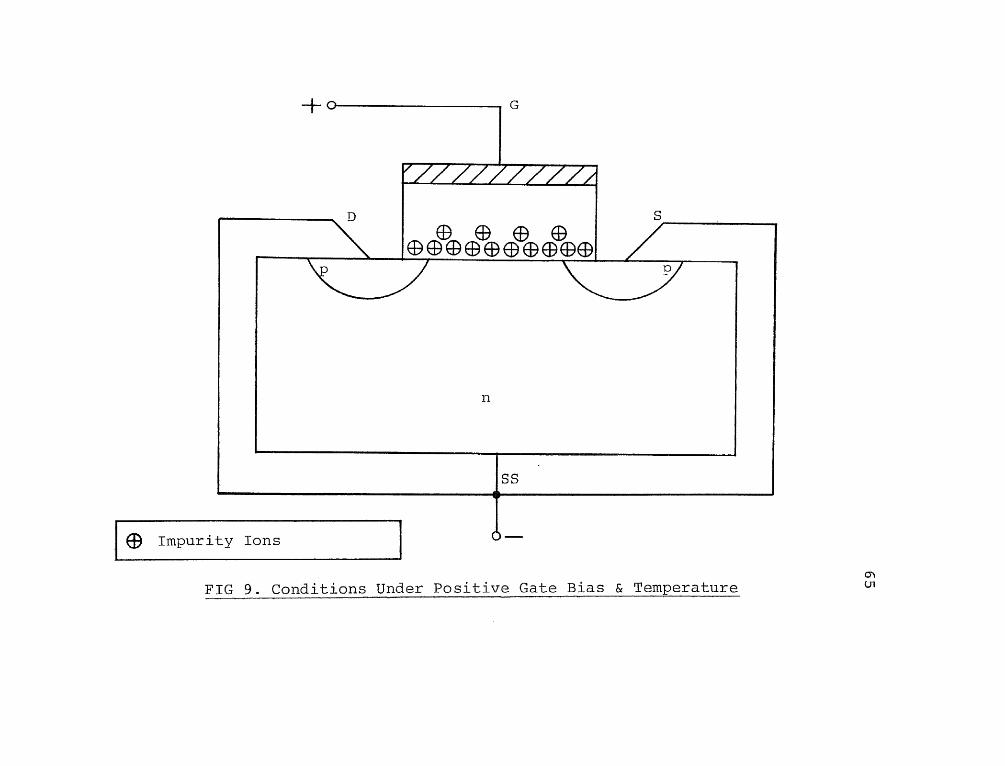
FIG 9, Conditions Under Positive Gate Bias & Temperature

Conditions at VT Measurement (+ve Gate Bias & Temp.)
FIG 10.
67temperature of 140 °C, the threshold voltage
of all the IIc units were found to drift towards
more negative values when the tests were
carried to 1100 hours. But tests at VGS = -28C
and 140°C (IIIa units) revealed CT drifts in
both directions upto 260 hours, but between
260 hours and the next set of readings taken
at 360 hours, all the units had drifted towards
more negative CT values. They continued to
do so beyond 360 hours also, and the drift even-
tually stabilized within 1200 hours. The same
pattern of drift was exhibited by the additional
IIIa units also.
A survey of the literature revealed that;
the papers of Deal et al103, Hofstein 104 , Reynolds
et al 105 , and Kim106 are relevant to the phenomena
observed, though none of them bring out explicity
the theoretical factors causing the observed thres-
hold voltage shifts. But taking the contents of
these four papers together and the experimental
results of this investigation, the occurence of
the following two competing mechanisms is herein
postulated:
1. Impurity ion migration: Under negative gate
68
bias, the electropositive impurity ions tend
to migrate towards the metal-oxide interface.
The consequent decrease in the positive ionic
charge density near the oxide-silicon inter-
face helps channel inversion, and hence
only a lower applied negative gate voltage is
required for channel inversion, or |VT| tends
to decrease. This can also be seen from the
expression for VT given in section 2.3. This
migration phenomenon should saturate, if the
bias stress is continued for sufficient
length of time, once all the available impurity
ions have migrated to the metal-oxide inter-
face.
2. Augmentation of positive charge density at the
oxide-silicon interface: Since the thermal
oxidation process itself takes place by the
inward diffusion of oxygen through the silicon
dioxide already formed in the outer layers, it
is inevitable that the last two hundred ang-
stroms or so of the oxide layer near the oxide-
silicon interface are only partially oxidized,
leaving some SiO atoms and some unoxidized Si
atoms. If a high enough negative field at
elevated temperature is applied across
the oxide, these unoxidized Si atoms are
69positively ionized. The silicon in the partially
oxidized zone could also be considered as
providing traps for holes. A high enough negative
gate bias at high temperature can also attract
into the oxide layer more positively ionized Si
from the substrate regions near the interface. The
net effect of all these is to cause an increase
in the positive ionic charge density at the oxide-
semiconductor interface. Such an augmentation of
positive charge density at the oxide-silicon inter-
face tends to oppose channel inversion. In other
words, |VT| will tend to increase.
Figures 11 and 12 depict the combined picture of the
conditions under negative gate bias and temperature,
and the conditions under VT measurement respectively.
Considering the ion migration mechanism, Marciniak
and Przewlocki 107 obtained drift time constants for
positive bias and temperature one or two orders of
magnitude higher than those for the opposite polarity,
and attributed their results to a possible trapping of
mobile ions at the metal-oxide interface. If this
theory is valid, it would follow that the increase in
|VT| due to ion migration in the negative bias case wouldbe less in magnitude and saturate faster, than in the
case of positive bias. This is consistent with the
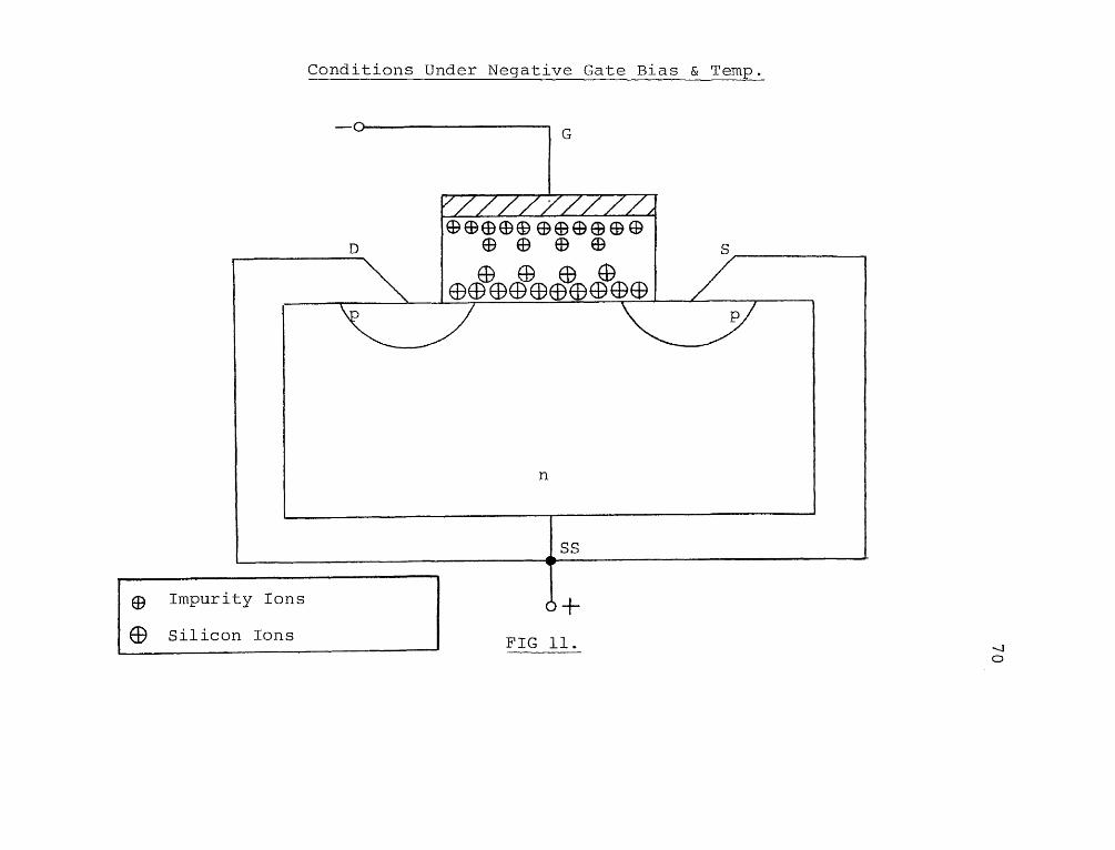
Conditions Under Negative Gate Bias & Temp.
FIG 11.

Conditions at VT Measurement (-ye Gate Bias & Temp.)
FIG 12.
72results obtained on the 260 hours test of category
IIIa and IIIb units.
Considering the latter mechanism, the presence of
the unoxidized silicon is believed also to be the
cause of QSS108. Under negative bias, the positive
charging of the unoxidized silicon increases the
threshold voltage magnitude. Deal 109 found that
at 300°C, the drift with time reached 90 percent of
the saturation value within 10 minutes and the
remaining 10 percent took 8 hours, when the applied
field was between 0.5 x 10 6 to 3.0 x 10 -6 V/cm. At
the 140 °C temperature and 2.3 x 10 -6 C/cm field used
in the tests of this study, this period can be expected
to be much longer.
The period required for the saturation of the
drift due to the second mechanism is much longer than
that required for the stabilization of the drift due
to the first mechanism. Thus, when the test duration
is small, either of the two competing mechanisms could
dominate; while for longer test duration, the second
effect becomes dominant at least after a few tens or
hundreds of hours. Thus, the threshold voltage drifts
eventually towards more negative values. The postulation
set forth is thus consistent with the test results
7 3presented in chapter IV.
74CHAPTER VI
CONCLUSIONS AND RECOMMENDATIONS
6.1. Conclusions:
P-channel MOSFET's under negative gate bias
and temperature stress may often show a downward
drift in IVT 1I initially, meaning a few tens to
a few hundreds of hours, depending on the field,
temperature, and impurity concentration. But
after this period, the drift in |VT| is upward.
The reason for this is that the migration of
impurity ions in the oxide layer predominates
initially over the positive ion augmentation
effect, while as time progresses, the latter
has the dominant effect.
For the positive gate bias and temperature
stress however, the drift in IVT I is upward through-out.
6.2. Recommendations:
During the manufacturing process, contamina-
tion by ionic impurities should be eliminated or
reduced to a minimum. Advances have been made
by the industry in this direction, but sustaining
the necessary process controls can not be over-

75emphasized.
Further studies are required to determine what
part of the augmentation of positive charge density
at the silicon-silicon dioxide interface is due
to the infusion of additional silicon ions into
the oxide from the substrate, and what part is
due to additional charging of ionized silicon
responsible for QSS.

76REFERENCES
1. Shockley,W., bibliography 52-1
2. Dacey,G.C. and Ross,I.M., bibliogrpahy 55-1
3. Schwartz,B. and Levy,M., bibliography 60-1
4. Weimer,P.K., bibliography 62-1
5. Ihantola,H.K.J. bibliography 61-1
6. Hofstein,S.R. and Heiman,F.P., bibliography 63-9
7. Wallmark,J.T., bibliography 64-13
8. Bockemuehl,R.R., bibliography 63-3
9. Evans,A.D., bibliography 63-7
10. Sah,C.T., bibliography 64-10
11. Sah,C.T., and Pao,H.C., bibliography 66-23
12. Wallmark,J.T., and Johnson,H., bibliography 66-7
13. Przybylski, et al, bibliography 66-19
14. Carr,W.N. and Mize,J.P., bibliography 72-1
15. Penney,W.M. and Lau,L., bibliography 72-13
16. Polinsky,M. and Graf,S., bibliography 73-7
17. Seely,J.L., bibliography 67-20
18. Mai,C.C. and Looney,J.C., bibliography 66-17
19. Powell,R.J., et al, bibliography 74-9
20. Gaind,A.K., et al, bibliography 76-4
21. Cocca,F.J. and Carrol,K.G., bibliography 68-4
22. Zak Zouk,A.K., et al, bibliography 76-20
23. Deal,B.E., bibliography 74-4
77
24. Richman,P., bibliography 73-9
25. Nicollian,E.H. and Goetzberger,A.bibliography 67-14
26. Brown,D.M. and Gray,P.V., bibliography 68-3
27. Gray,P.V. and Brown,D.M., bibliography 66-11
28. Castro,P.L. and Deal,B.E., bibliography 71-1
29. Zaininger,K.H. and Warfield.G.G. bibliography 64-14
30. Olmstead,J., et al, bibliography 65-16
31. Grove,A.S., et al, bibliography 65-4
32. Nicollian,E.H., et al, bibliography 69-15
33. Deal,B.E., et al, bibliography 67-5
34. Revesz,A.G. and Zaininger,K.H.,bibliography 66-20
35. Hofstein,S.R., bibliography 66-13
36. Yon,E., et al, bibliography 66-27
37. Sugano,T., et al, bibliography 68-16
38. Snow,E.H., et al, bibliography 65-21
39. Goetzberger,A., bibliography 66-8
40. Hofstein,S.R., bibliography 67-10
41. Lindmeyer,J., bibliography 66-16
42. Schlegel,E.S., et al, bibliography 68-15
43. Kriegler,R.J., et al, bibliography 72-9
44. Vincoff,M.N. and Schnable,G.L.,bibliography 75-11
45. Andre,B., et al, bibliography 69-1
46. Grove,A.S., et al, bibliography 64-4
47. Deal,B.E., et al, bibliography 65-3
7848. Revesz,A.G., bibliography 65-18
49. Berger,W.M., et al, bibliography 66-1
50. Lindmeyer,J., bibliography 66-16
51. Black,J.R., bibliography 69-3
52. Faggen,F. and Klein,T., bibliography 70-2
53. McMillan,R.E. and Misra,R.P., bibliography 70-14
54. Hu,S.M. and Gregor,L.V., bibliography 67-11
55. Frieser,R.G., bibliography 68-10
56. Curry,J.J. and Nigh,H.E., bibliography 70-5
57. Chau,N.J., et al, bibliography 72-2
58. Lundstrom,K.I.and Svensson,C.M., bibliography 72-10
59. Dockerty,R.C., et al, bibliography 75-4
60. Bower,R.W., et al, bibliography 68-2
61. Faggen,F. and Klein,T., bibliography 70-6
62. Laughton,W.J., bibliography 71-7
63. Mavor,J., bibliography 73-6
64. Mayer,J., et al, bibliography 70-12
65. Shannon,J.M., et al, bibliography 69-22
66. Bower,R.W., et al, bibliography 68-2
67. Nishimatsu,S., et al, bibliography 71-11
68. Sansbury,J.D., bibliography 73-11
69. Douglas,E.C. and Dingwall,G.F., bibliography 74-5
70. Pocha,M.D., et al, bibliography 74-8
71. Misra,R.P., bibliography 64-9

7972. Eliot,C.C., bibliography 67-6
73. Philco Ford Report, bibliography 67-16
74. Rand,H.T. and Kelem,L.S., bibliography 69-17
75. Vincoff,M.N. and Schnable,G.L.,bibliography 75-11
76. Hawkins,R., bibliography 76-7
77. Clark,L., et al, bibliography 67-4
78. Workman,W., bibliography 68-17
79. Schnable,G.L. and Keen,R.S., bibliography 69-20
80. Rand,H.T., bibliography 70-17
81. Workman,W., bibliography 65-23
82. Thornton,P.R., et al, bibliography 69-24
83. Goetzberger,A., bibliography 66-9
84. Reinhartz,K.K., et al, bibliography 65-17
85. Berger,W.M., et al, bibliography 66-1
86. Ficchi,R.F., bibliography 66-6
87. Bast,G.E., et al, bibliography 65-2
88. Reynolds,F.H., et al, bibliography 70-18
89. Carr,W.N. and Mize,J.P., bibliography 72-1
90. Deal,B.E., et al, bibliography 67-5
91. Carr,W.N. and Mize,J.P., bibliography 72-1
92. Rand,H.T. and Kelem,L.S., bibliography 69-17
93. Grove,A.S., bibliography 67-8
94. Iyer,R.R., bibliography 68-11
95. Lenzlinger,M., bibliography 71-8
8096. Gregor,L.V., bibliography 66-12
97. Snow,E.H., et al, bibliography 65-21
98. Deal,B.E., bibliography 74-4
99. Hofstein,S.R., bibliography 66-13
100. Misra,R.P., bibliography 64-9
101.McMillan,R.E. and Misra,R.P. bibliography 70-14
102. Deal,B.E., bibliography 74-4
103. Deal,B.E., et al, bibliography 67-5
104. Hofstein,S.R., bibliography 67-10
105. Reynolds,F.H., et al, bibliography 70-18
106. Kim,M.J. bibliography 69-13
107. Marciniak, and Przewlocki, bibliography 76-12
108. Deal,B.E., et al, bibliography 67-5
109. Personal Correspondence with Bruce E. Deal, June 1972.
APPENDIX A. EXTRACT OF SCREENING PROCEDURE, MIL-STD-883A, METHOD 5004.2
SCREENCLASS B
MIL-STD-883 REQUIREMENTCONDITIONMETHOD (% )
3.1.1 INTERNAL CISUAL(PRECAP)
2010 TEST CONDITION B 100
3.1.2 STABILIZATION BAKE 1008 24 HRS MIN TEST 100CONDITION C MIN
3.1.3 THERMAL SHOCK 1011 -
3.1.4 TEMPERATURE CYCLING 1010 TEST CONDITION C 100MIN.
3.1.5 MECHANICAL SHOCK 2002 - -
3.1.6 CONSTANTACCELERATION
2001 TEST CONDITION E 100(MIN) Yl PLANE
3.1.7 HERMETICITYa. FINE b. GROSS
1014 - 100
3.1.8 INTERIM (PRE-BURN-IN)ELECTRICALPARAMETERS
PER APPLIC- PER APPLICABLEABLE PROCURE- - DOCUMENTMENT DOCUMENT
3.1.9 BURN-IN TEST 1015 160 HOURS AT 100125°C MIN.
CO

SCREEN
CLASS B
MIL-STD-883 CONDITION REQUIREMENTMETHOD (% )
3.1.10 INTERIM(POST-BURN-IN)ELECTRICALPARAMETERS
PER APPLICABLEPROCUREMENT - -DOCUMENT
3.1.11 REVERSE-BIAS BURN-IN 1015 TEST CONDITION AOR C, WHEN SPECI- -FIED 72 HRS. AT150°C MIN.
3.1.12 FINAL ELECTRICALTEST a. STATIC TESTS1. 25°C 2. MAX ANDMIN RATED OPERATINGTEMPERATUREb. DYNAMIC TESTS25°C
PER APPLICABLE - 100PROCUREMENTDOCUMENT
3.1.13 RADIOGRAPHIC - - -
3.1.14 QUALIFICATION ORQUALITY CONFORMANCEINSPECTION TESTSAMPLE SELECTION
5005 - PERAPPLICABLEDOCUMENT
3.1.15 EXTERNAL VISUAL 2009 - 100 OD
83APPENDIX B.
FAILURE MODES OF MOS DEVICES
1. Defects due to electrical overstress:
1.1. Open bond wires1.2. Punctured gate oxide1.3. Blown protective devices
2. Oxide faults:
2.1. Pinholes2.2. Cracks2.3. Contamination
3. Metallization faults:
3.1. Lifting metal3.2. Over-alloying3.3. Cracks in metal3.4 Too thin metal3.5. Bridging metal3.6. Corroded metal
4. Surface defects:
4.1. Contamination, ionic and particulate4.2. Excessive accumulation or depletion4.3. Inversion or channeling
5. Die-mount faults:
5.1. Misplaced die5.2. Poor adhesion and voids under die5.3. Eutectic on die
6. Wire-bonding faults:
6.1. Broken wire6.2. Mis-targeted bonds6.3. Improper ball size6.4. Excessive wire tails6.5. Excessive slackness6.6. Crossing of wires6.7. Poor bond-pull strength6.8. Purple plaque
84
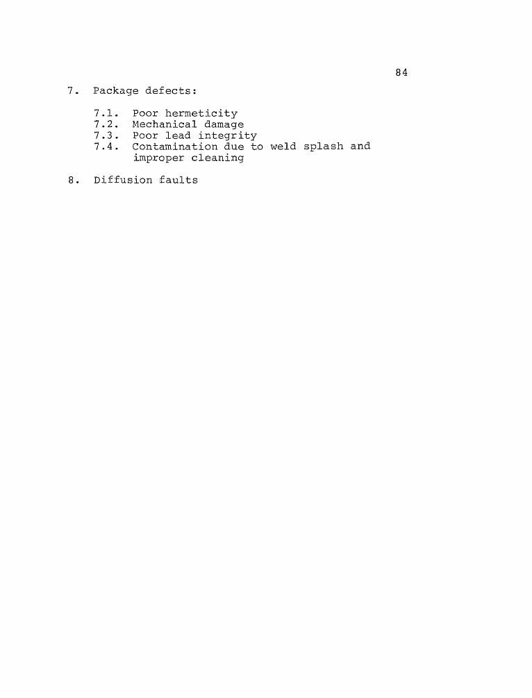
7. Package defects:
7.1. Poor hermeticity7.2. Mechanical damage7.3. Poor lead integrity7.4. Contamination due to weld splash and
improper cleaning
8. Diffusion faults
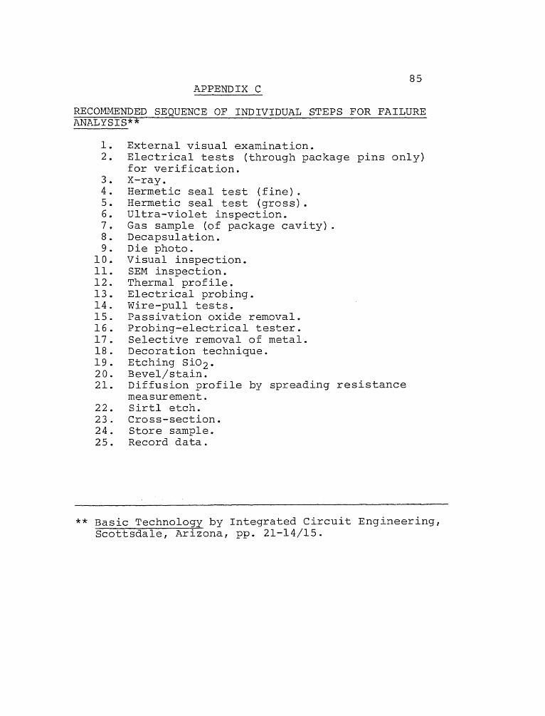
85APPENDIX C
RECOMMENDED SEQUENCE OF INDICIDUAL STEPS FOR FAILURE ANALYSIS**
1. External visual examination.2. Electrical tests (through package pins only)
for verification.3. X-ray.4. Hermetic seal test (fine).5. Hermetic seal test (gross).6. Ultra-violet inspection.7. Gas sample (of package cavity).8. Decapsulation.9. Die photo.
10. Visual inspection.11. SEM inspection.12. Thermal profile.13. Electrical probing.14. Wire-pull tests.15. Passivation oxide removal.16. Probing-electrical tester.17. Selective removal of metal.18. Decoration technique.19. Etching Si02.20. Bevel/stain.21. Diffusion profile by spreading resistance
measurement,22. Sirtl etch.23. Cross-section.24. Store sample.25. Record data.
** Basic Technology by Integrated Circuit Engineering,Scottsdale, Arizona, pp. 21-14/15.
86
APPENDIXD
SUMMARY OF BASIC FAILURE ANALYSIS TECHNIQUES ***
*** Basic Technology by Integrated Circuit Engineering,Scottsdale, Arizona, pp. 21-36/37.
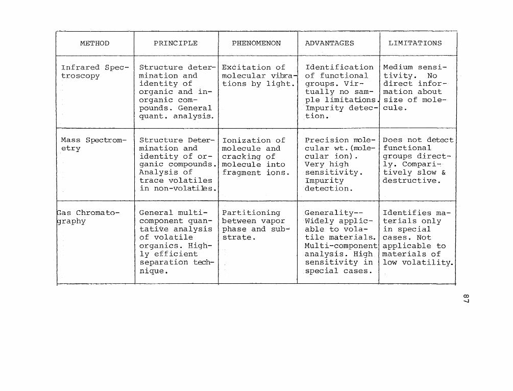
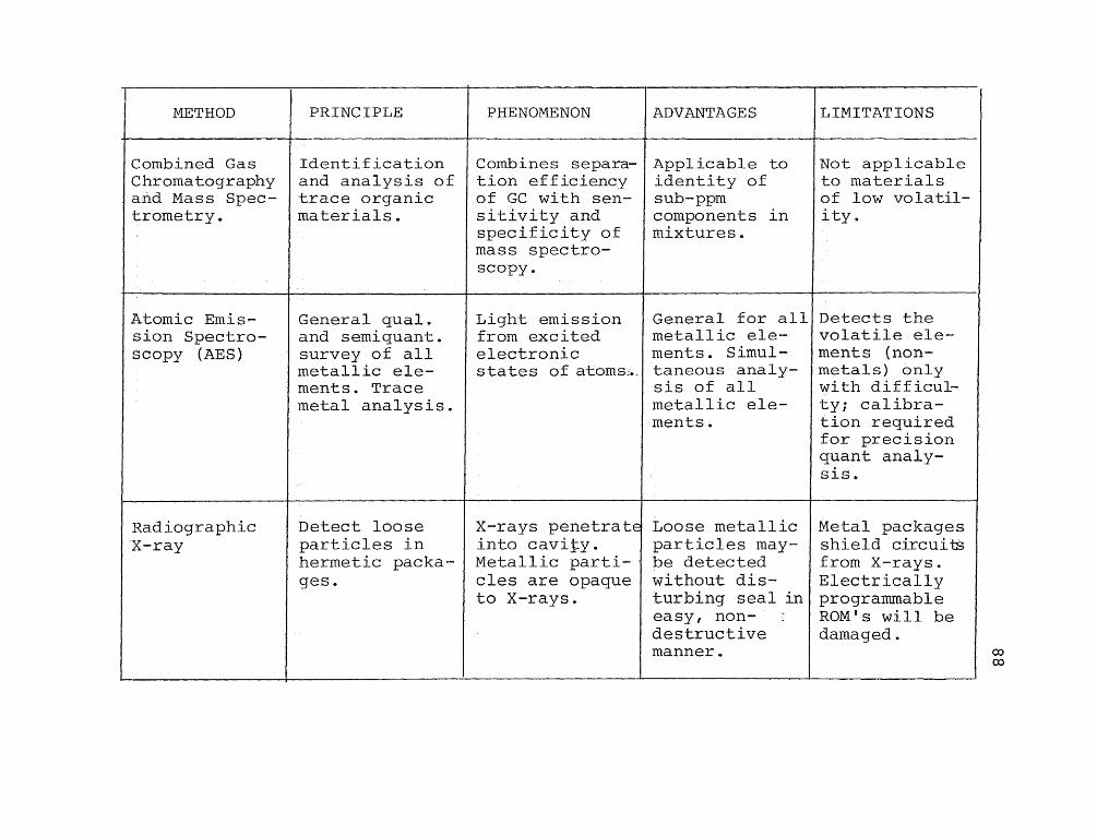
METHOD PRINCIPLE PHENOMENON ADVANTAGES LIMITATIONS
Infrared Spec-troscopy
Structure deter-mination andidentity oforganic and in-organic com-pounds. Generalquant. analysis.
Excitation ofmolecular vibrations by light.
Identificationof functionalgroups. Cir-tually no sam-ple limitations.Impurity detec-tion.
Medium sensi-tivity. Nodirect infor-mation aboutsize of mole-cule.
Mass Spectrom-etry
Structure Deter-mination andidentity of or-ganic compounds.Analysis oftrace volatilesin non-volatiles.
Ionization ofmolecule andcracking ofmolecule intofragment ions.
Precision mole-cular wt.(mole-cular ion).Very highsensitivity.Impuritydetection.
Does not detectfunctionalgroups direct-ly. Compari-tively slow &destructive.
Gas Chromato-graphy
General multi-component quan-tative analysisof volatileorganics. High-ly efficientseparation tech-nique.
Partitioningbetween vaporphase and sub-strate.
Generality--Widely applic-able to vola-tile materials.Multi-componentanalysis. Highsensitivity inspecial cases.
Identifies ma-terials onlyin specialcases. Notapplicable tomaterials oflow volatility.
CO
METHOD PRINCIPLE PHENOMENON ADVANTAGES LIMITATIONS
Combined GasChromatographyand Mass Spec-trometry.
Identificationand analysis oftrace organicmaterials.
Combines separa-tion efficiencyof GC with sen-sitivity andspecificity ofmass spectro-scopy.
Applicable toidentity ofsub-ppmcomponents inmixtures.
Not applicableto materialsof low volatil-ity.
Atomic Emis-lion Spectro-scopy (AES)
General qual.and semiquant.survey of allmetallic ele-ments. Tracemetal analysis.
Light emissionfrom excitedelectronicstates of atoms-.
General for allmetallic ele-ments. Simul-taneous analy-sis of allmetallic ele-ments.
Detects thevolatile ele-ments (non-metals) onlywith difficul-ty; calibra-tion requiredfor precisionquant analy-sis.
RadiographicX-ray
Detect looseparticles inhermetic packa-ges.
X-rays penetrateinto cavity.Metallic parti- -
Iles are opaqueto X-rays.
Loose metallicparticles may-be detectedwithout dis-turbing seal ineasy, non-destructivemanner.
Metal packagesshield circuitsfrom X-rays.ElectricallyprogrammableROM's will bedamaged.
OD03

METHOD PRINCIPLE PHENOMENON ADVANTAGES LIMITATIONS
Leak Test Determine her-miticity ofpackages.
Fine leak testsforce detect-able materialin package anddetects itsescape.
Eliminatespossible fieldfailures anddeterminespossible causeof faileddevices.
Correlationbetween leakrate and fail-ure rate notdocumented.
Spreading Re-sistance
Measures resis -
tivity.Resistance be-tween two probesis function ofproble charac-teristics,resistivity &geometry ofmaterial
High spatialresolution canbe obtained.
Calibration ofprobe charac-teristics andproper surfacepreparation ofchip is essen-tial.
Plasma Etching Remove glassi-vation. Alsoused to removesilicon,
Ionized fluorineetch attacksSi02 and Si ¬ aluminum
Removes glass-ivation with-out damagingaluminum metal-lization oradding othercontaminants.
Requires addit-Tonal equipment
00
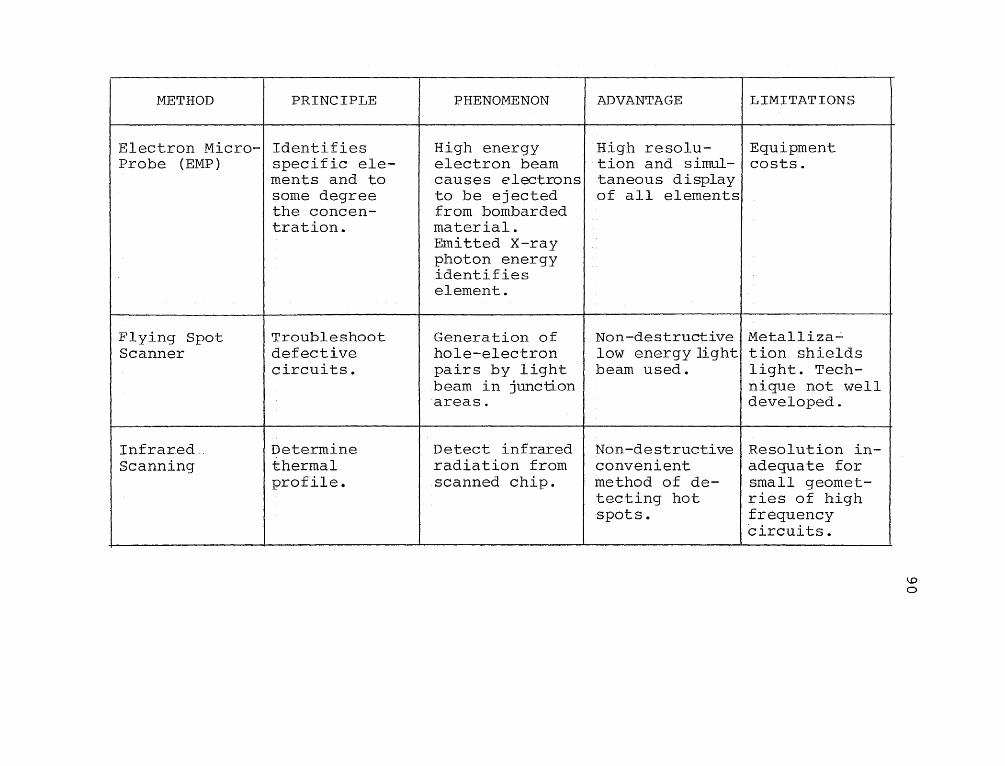
METHOD PRINCIPLE PHENOMENON ADVANTAGE LIMITATIONS
Electron Micro-Probe (EMP)
Identifiesspecific ele-ments and tosome degreethe concen-tration.
High energyelectron beamcauses electronsto be ejectedfrom bombardedmaterial.Emitted X-rayphoton energyidentifieselement.
High resolu-tion and simul-taneous displayof all elements
Equipmentcosts.
Flying SpotScanner
Troubleshootdefectivecircuits.
Generation ofhole-electronpairs by lightbeam in junctionareas.
Non-destructivelow energy lightbeam used.
Metalliza-tion shieldslight. Tech-pique not welldeveloped.
InfraredScanning
Determinethermalprofile.
Detect infraredradiation fromscanned chip.
Non-destructiveconvenientmethod of de-tecting hotspots.
Resolution in-adequate forsmall geomet-ries of highfrequencycircuits.

91APPENDIX E
SPECIFICATIONS OF AMI DD07P, DD07K, DD08P, AND DD08K MOSFETs
General Description: Medium Conductance P-channel
Enhancement Mode MOSFET's in
TO-72 Package.
Terminal Diagrams - Bottom View
Absolute Maximum Ratings (TA = 25 °C, Body Grounded)

SYMBOLI
CHARACTERISTICS MIN. TYP. MAX. UNITS TEST CONDITIONS
VT Threshold Voltage -3.5 -4.3 5.5 V VGS = VDS , IDS = -10 uA
BCDSS Drain-Source Breakdown -30 -41 - V IDS = -10 uA, VGS = 0
BVSDS Source-Drain Breakdown -30 -41 - V IsD = -10uA, VGD = 0
BVPNG Body Breakdown -30 -41 - V IDB = -10uA, VGS = 0,Source Open
BVGSS* Gate-Source Breakdown -30 -41 - V IGs = -10uA, VDS = 0
IDSS Drain Leakage - 0.05 1.0 nA VDS = -15V, VGS = 0
ISDS Source Leakage - 0.07 1.0 nA VSD = 15V, VGD = 0
I GSS* Gate Leakage - 0.01 1.0 nA VGS = -15V, VDS = 0
IGSS Gate Leakage - 0.1 - pA VGS = -30V, VDS = 0
IDSon ON Drain Current 15.5 44.0 - mA VGS = VDS = -15V
RON DC ON Resistance - 125 200 ohms VGS = -15V, VDS =--010V
Yfs Forward Transadmittance 14000 5400 - umho VGS = -15V, VDs=-15V,F = 1.0 kHz
rd Dynamic Drain Resistance - 2.0 - kohm VGS = -15V, VDs=-15V,F = 1.0 kHz
Ciss Input Capacitance - 4.4 6.0 pF VGS = 0, VDS = 0
Coss1
Output Capacitance - 4.6 6.0 pF VGS = 0 , VDS = 0

SYMBOL CHARACTERISTICS MIN. TYP. MAX. UNITS I TEST CONDITIONS
Crss Reverse TransferCapacitance
- 0.60 1.00 pF VGS = 0, VDS = 0,Crss = Cgd
Cgs Gate-to-Source Capaci-tance
- 3.8 5.0 pF VGS = 0, VDS = 0
Cds Drain-to-Source Cap-acitance
- 4.0 5.0 pF VGS = 0, VDS= 0
Fi Input Gain Bandwidth
Frequency- 195 MHz. Fi = Yfs/2π Ci ss
Fo Output Gain BandwidthFrequency
187 - MHz Fo = Yfs/2π Coss
* With gate protective zener (DD07P, DD07K)
CU

9 4
APPENDIX F
TEST DATA ON ALL INDIVIDUAL DEVICES
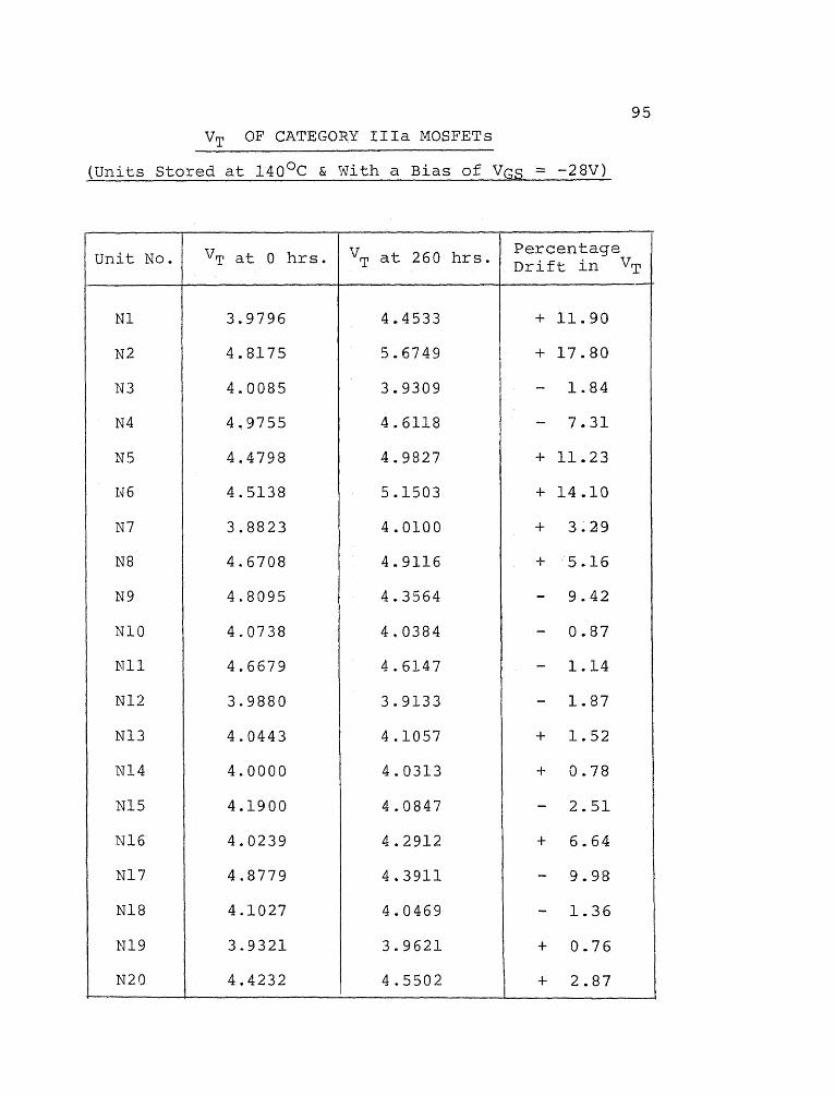
95
VT OF CATEGORY IIIa MOSFETs
(Units Stored at 140 °C & With a Bias of VGs = -28V)
Unit No. VT at 0 hrs. VT at 260 hrs.PercentageDrift in VT
N1 3.9796 4.4533 + 11.90
N2 4.8175 5.6749 + 17.80
N3 4.0085 3.9309 - 1.84
N4 4.9755 4.6118 - 7.31
N5 4.4798 4.9827 + 11.23
N6 4.5138 5.1503 + 14.10
N7 3.8823 4.0100 + 3.29
N8 4.6708 4.9116 + 5,16
N9 4.8095 4.3 .564 - 9.42
N10 4.0738 4.0384 - 0.87
N11 4.6679 4.6147 - 1.14
N12 3.9880 3.9133 1.87
N13 4.0443 4.1057 + 1.52
N14 4.0000 4.0313 + 0.78
N15 4.1900 4.0847 - 2.51
N16 4.0239 4.2912 + 6.64
N17 4.8779 4.3911 - 9.98
N18 4.1027 4.0469 - 1.36
N19 3.9321 3.9621 + 0.76
N20 4.4232 4.5502 + 2.87

96VT OF CATEGORY IIIa MOSFETS - continued
Unit No. at 0 hrs. VT at 260 hrs.PercentageDrift in CT
N21 5.2145 5.9066 + 13.27
N22 4.7600 4.3421 - 8.78
N23 3.9721 4.3820 + 10.32
Mean = 4.3654 4,4670
S.D. = 0.3996 0.5303
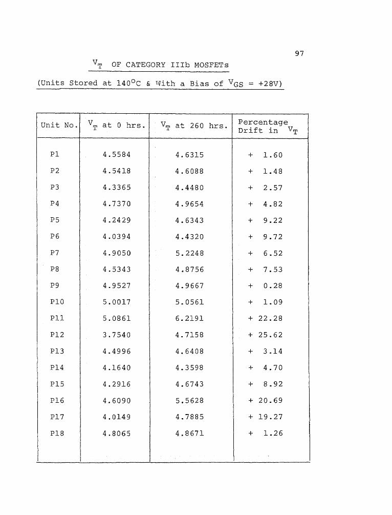
97
VT OF CATEGORY Mb MOSFETs
(Units Stored at 140 00 & With a Bias of VGS = +28C)
Unit No. VT at 0 hrs. at 260 hrs. Pe r centageDrift in VT
P1 4.5584 4.6315 + 1.60
P2 4.5418 4.6088 + 1.48
P3 4.3365 4.4480 + 2.57
P4 4.7370 4.9654 + 4.82
P5 4.2429 4.6343 + 9.22
P6 4.0394 4.4320 + 9.72
P7 4.9050 5.2248 + 6.52
P8 4.5343 4.8756 + 7.53
P9 4.9527 4.9667 + 0,28
P10 5.0017 5.0561 + 1.09
P11 5.0861 6.2191 + 22.28
P12 3.7540 4.7158 + 25.62
P13 4.4996 4.6408 + 3.14
P14 4.1640 4.3598 + 4.70
P15 4.2916 4.6743 + 8.92
P16 4.6090 5.5628 + 20.69
P17 4.0149 4.7885 + 19.27
P18 I 4.8065 4.8671 + 1.26
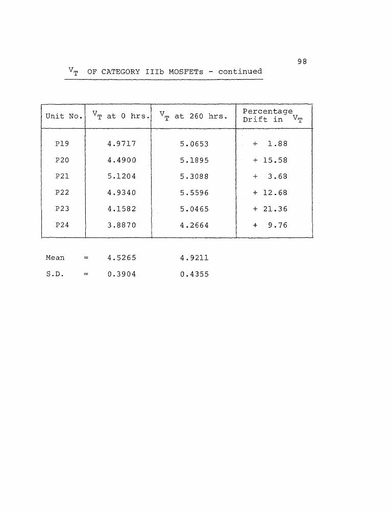
98VT OF CATEGORY IIIb MOSFETs - continued
Unit No. at 0 hrs. at 260 hrs .PercentageDrift in CT
P19 4.9717 5.0653 + 1.88
P20 4.4900 5.1895 + 15.58
P21 5.1204 5.3088 + 3.68
P22 4.9340 5.5596 + 12.68
P23 4.1582 5.0465 + 21.36
P24 3.8870 4.2664 + 9.76
Mean = 4.5265 4.9211
S.D. = 0.3904 0.4355
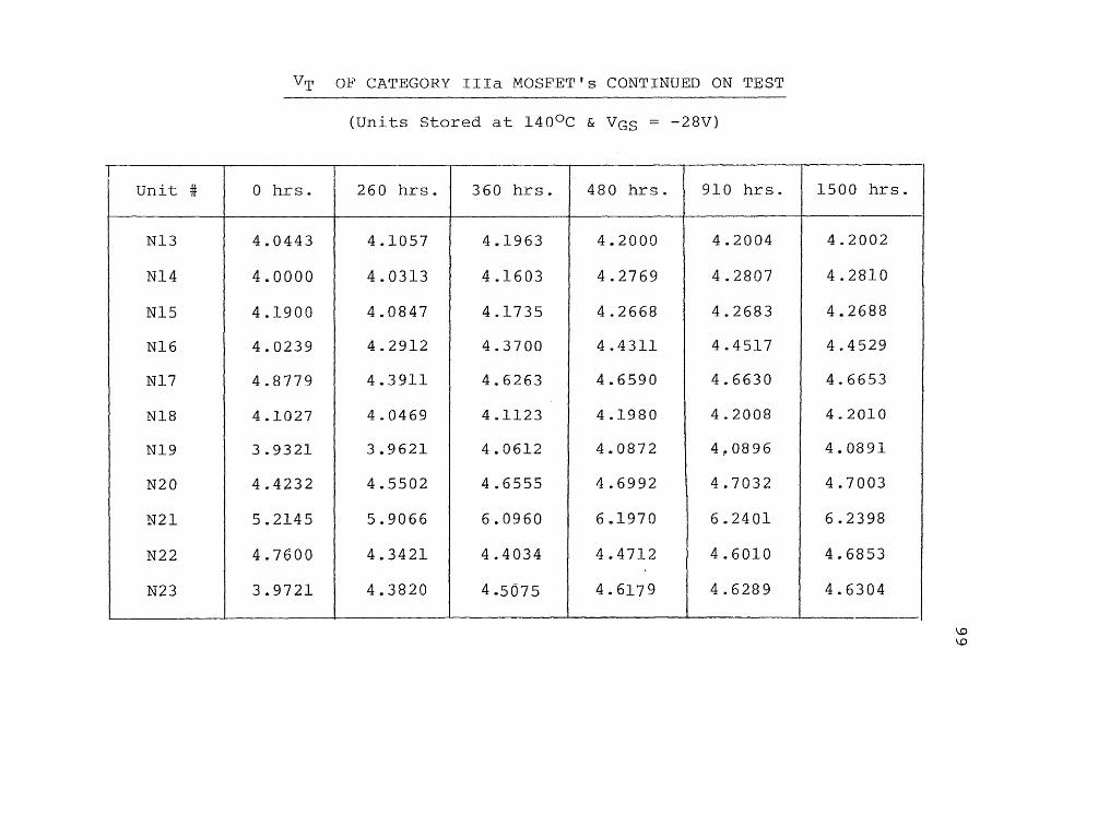
VT OF CATEGORY IIIa MOSFET's CONTINUED ON TEST
(Units Stored at 140 0C & VGS = -28V)
Unit # 0 hrs. 260 hrs. 360 hrs. 480 hrs. 910 hrs. 1500 hrs.
N13 4.0443 4.1057 4.1963 4.2000 4.2004 4.2002
N14 4.0000 4.0313 4.1603 4.2769 4.2807 4.2810
N15 4.1900 4.0847 4.1735 4.2668 4.2683 4.2688
N16 4.0239 4.2912 4.3700 4.4311 4.4517 4.4529
N17 4.8779 4.3911 4.6263 4.6590 4.6630 4.6653
N18 4.1027 4.0469 4.1123 4.1980 4.2008 4.2010
N19 3.9321 3.9621 4.0612 4.0872 4,0896 4.0891
N20 4.4232 4.5502 4.6555 4.6992 4.7032 4.7003
N21 5.2145 5.9066 6.0960 6.1970 6.2401 6.2398
N22 4.7600 4.3421 4.4034 4.4712 4.6010 4.6853
N23 3.9721 4.3820 4.5075 4.6179 4.6289 4.6304
9
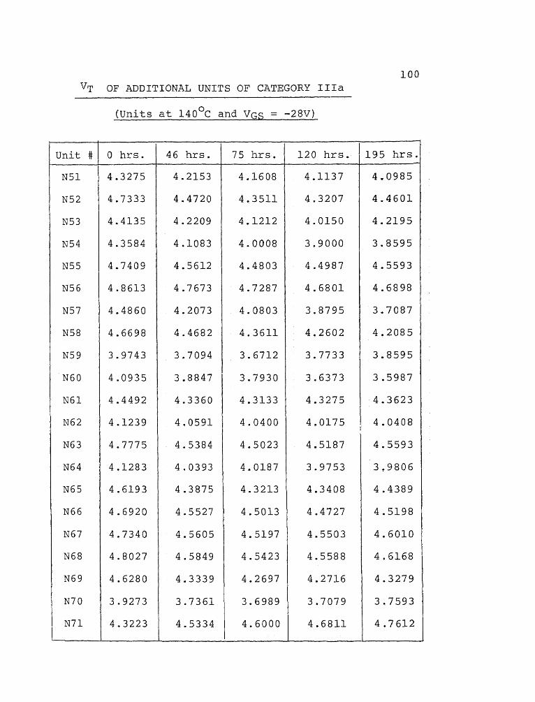
100VT OF ADDITIONAL UNITS OF CATEGORY IIIa
(Units at 140 °C and VGA -28C)
Unit #
N51
0 hrs.
4.3275
46 hrs.
4.2153
75 hrs.
4.1608
120 hrs.
4.1137
195 hrs.
4.0985
N52 4.7333 4.4720 4.3511 4,3207 4.4601
N53 4.4135 4.2209 4.1212 4.0150 4.2195
N54 4.3584 4.1083 4.0008 3.9000 3.8595
N55 4.7409 4.5612 4.4803 4.4987 4.5593
N56 4.8613 4.7673 4.7287 4.6801 4.6898
N57 4.4860 4.2073 4.0803 3.8795 3.7087
N58 4.6698 4.4682 4.3611 4,2602 4.2085
N59 3.9743 3.7094 3.6712 3.7733 3.8595
N60 4.0935 3.8847 3.7930 3.6373 3.5987
N61 4.4492 4.3360 4.3133 4.3275 4.3623
N62 4.1239 4,0591 4.0400 4,0175 4.0408
N63 4.7775 4.5384 4.5023 4.5187 4.5593
N64 4.1283 4.0393 4.0187 3.9753 3.9806
N65 4.6193 4.3875 4.3213 4.3408 4.4389
N66 4.6920 4.5527 4.5013 4.4727 4.5198
N67 4.7340 4.5605 4.5197 4.5503 4.6010
N68 4.8027 4.5849 4.5423 4.5588 4,6168
N69 4.6280 4.3339 4.2697 4.2716 4.3279
N70 3.9273 3.7361 3.6989 3.7079 3.7593
N71 4.3223 4.5334 4.6000 4.6811 4.7612
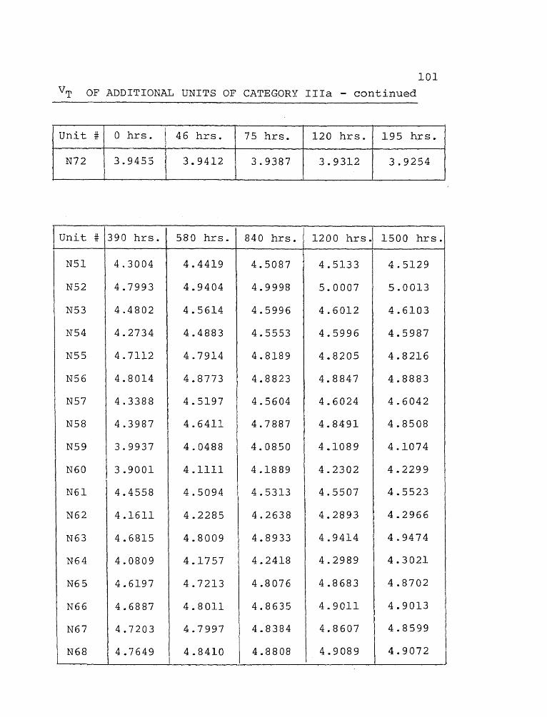
101
VT OF ADDITIONAL UNITS OF CATEGORY IIIa - continued
Unit # 0 hrs. 46 hrs. 75 hrs. 120 hrs. 195 hrs.
N72 3.9455 3.9412 3.9387 3.9312 3.9254
Unit # 390 hrs. 580 hrs. 840 hrs. 1200 hrs. 1500 hrs.
N51 4,3004 4.4419 4.5087 4.5133 4.5129
N52 4.7993 4.9404 4.9998 5.0007 5.0013
N53 4.4802 4.5614 4.5996 4.6012 4.6103
N54 4.2734 4.4883 4.5553 4.5996 4.5987
N55 4.7112 4.7914 4.8189 4.8205 4.8216
N56 4.8014 4.8773 4.8823 4.8847 4.8883
N57 4.3388 4.5197 4.5604 4.6024 4.6042
N58 4.3987 4.6411 4.7887 4.8491 4.8508
N59 3.9937 4.0488 4.0850 4.1089 4.1074
N60 3.9001 4.1111 4.1889 4.2302 4.2299
N61 4.4558 4.5094 4.5313 4.5507 4.5523
N62 4.1611 4.2285 4.2638 4.2893 4.2966
N63 4.6815 4.8009 4.8933 4.9414 4.9474
N64 4.0809 4.1757 4.2418 4.2989 4.3021
N65 4.6197 4.7213 4.8076 4.8683 4.8702
N66 4.6887 4.8011 4.8635 4.9011 4.9013
N67 4.7203 4.7997 4.8384 4.8607 4.8599
N68 4.7649 4.8410 4.8808 4.9089 4.9072
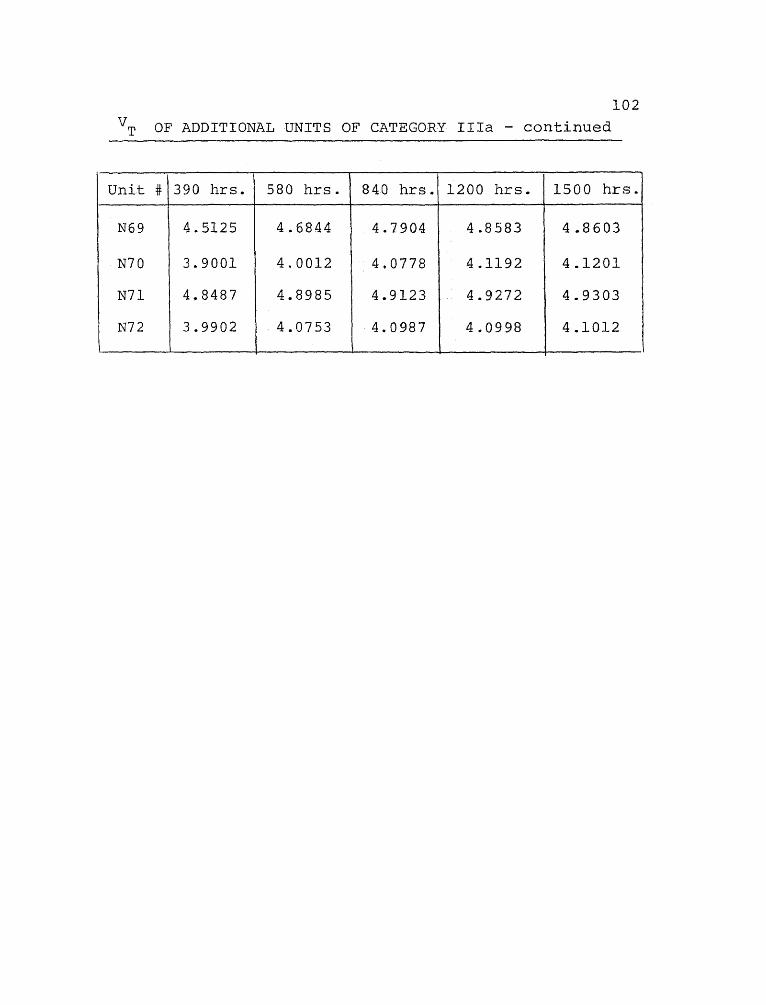
102
VT OF ADDITIONAL UNITS OF CATEGORY IIIa - continued
Unit # 390 hrs. 580 hrs. 840 hrs. 1200 hrs. 1500 hrs.
N69 4.5125 4.6844 4.7904 4.8583 4.8603
N70 3.9001 4.0012 4.0778 4.1192 4.1201
N71 4.8487 4.8985 4.9123 4.9272 4.9303
N72 3.9902 4.0753 4.0987 4.0998 4.1012
103
APPENDIX G
THRESHOLD VOLTAGE DEFINITIONS
The definitions and expressions for C T , given in
chapter II, are based on the assumption that conduction
is deemed to have commenced, when the channel surface
has become as much p in nature as the bulk is n. In
section 2.2, VT is hence defined as the gate voltage
required to produce sufficient Q G to counteract the
surface state charge QSS and the charge QD of a
depletion region that supports a potential of 2.4.
In figure 2, the same definition is expressed in terms
of charge distributions as below:
In the expression for VT given in section 2.3, the term
QB (charge density in the bulk silicon) is equal to
(QD + Q 1 ), the total hole charge in the depletion region
and the inverted channel, due to the applied gate volt-
age. This expression also includes terms to take into
account the effects of (i) the work function difference
between the gate metal and the silicon and (ii) any ionic
contamination in the gate oxide.
104
BIBLIOGRAPHY
(arranged in reverse chronological order)
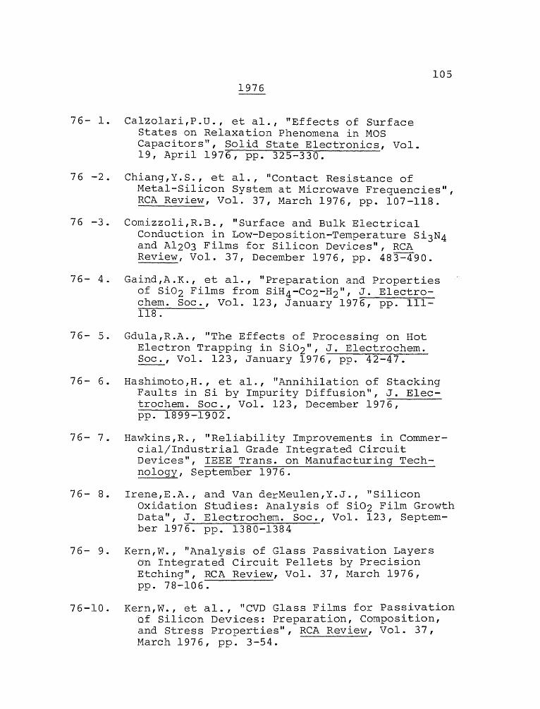
1051976
76- 1. Calzolari,P.U., et al., "Effects of SurfaceStates on Relaxation Phenomena in MOSCapacitors", Solid State Electronics, Col.19, April 1976, pp. 325-330.
76 -2. Chiang,Y.S., et al., "Contact Resistance ofMetal-Silicon System at Microwave Frequencies",RCA Review, Vol. 37, March 1976, pp. 107-118.
76 -3. Comizzoli,R.B., "Surface and Bulk ElectricalConduction in Low-Deposition-Temperature Si3N4and Al203 Films for Silicon Devices", RCAReview, Vol. 37, December 1976, pp. 483-490.
76- 4. Gaind,A.K., et al., "Preparation and Propertiesof Si02 Films from SiH4-Co2-H2", J. Electro-chem. Soc., Vol. 123, January 1976, pp. 111-118.
76- 5. Gdula,R.A., "The Effects of Processing on HotElectron Trapping in Si02", J. Electrochem. Soc., Vol. 123, January 1976, pp. 42-47.
76- 6. Hashimoto,H., et al., "Annihilation of StackingFaults in Si by Impurity Diffusion", J. Elec-trochem. Soc., Vol. 123, December 1976,pp. 1899-1902.
76- 7. Hawkins,R., "Reliability Improvements in Commer-cial/Industrial Grade Integrated CircuitDevices", IEEE Trans. on Manufacturing Tech-nology, September 1976.
76- 8. Irene,E.A., and Van derMeulen,Y.J., "SiliconOxidation Studies: Analysis of Si02 Film GrowthData", J. Electrochem. Soc., Vol. 123, Septem-ber 1976. pp. 1380-1384
76- 9. Kern,W., "Analysis of Glass Passivation Layerson Integrated Circuit Pellets by Precision
Etching", RCA Review, Vol. 37, March 1976,pp. 78-106.
76-10. Kern,W., et al., "CVD Glass Films for PassivationOf Silicon Devices: Preparation, Composition,and Stress Properties", RCA Review, Col. 37,March 1976, pp. 3-54.

10676-11. Kroell,K.E., and Ackerman,G.K., "Threshold
Voltage of Narrow Channel Field Effect Trans-istors", Solid State Electronics, Vol. 19,January 1976, pp. 77-82.
76-12. Marciniak,W., and Przewlocki,H.M., "On theBehavior of Mobile Ions in Dielectric Layersof MOS Structures", J. Electrochem. Soc.,Vol. 123, August 1976, pp. 1207-1212.
76-13. Nakhmanson,R.S., "On the Theory of MIS Capaci-tance", Solid State Electronics, Vol.19,September 1976, pp. 745-758.
76-14. Pierret,R.F., "Photo-Thermal Probing of Si-Si02Surface Centers, I. Theory and II. Experiment",Solid State Electronics, Vol. 19, July 1976,pp. 577-604.
76-15. Raymond,R.K., and Das,M.B., "Fabrication andCharacteristics of MOS-FET's IncorporatingAnodic Aluminum Oxide in the Gate Structure",Solid State Electronics, Vol. 19, March 1976,pp. 181-190.
76-16. Simmons,J.G., and Wei,L.S., "Non-Steady-StateBulk-Generation Processes in Pulsed Metal-Insulator-Semiconductor Capacitors", Solid State Electronics, Vol. 19, February 1976,pp. 153-158.
76-17. Stapper,C.H., "LSI Yield Modeling and ProcessMonitoring", IBM J. Research and Development,Vol. 20, May 1976, pp. 228-234.
76-18. Tsao,K.Y., and Leenov,D., "On Nonequilibrium C-VCharacteristics of MOS Inversion Region", Solid State Electronics, Vol. 19, January 1976,pp. 27-30.
76-19. Uranwala,J.S., et al., "The Determination ofthe Energy Distribution of Interface Traps inMetal-Nitride-Oxide-Silicon (memory) DevicesUsing Non-Steady-State Techniques", Solid State Electronics, Vol. 19, May 1976, pp. 375-380.
76-20. Zak Zouk,A.K., et al., "The Nature of Defects inSilicon Dioxide", J. Electrochem, Soc., Vol. 123,October 1976, pp. 1551-1555.

107
1975
75- 1. Arai,M., "Charge-Storage Junction Field-EffectTransistor", IEEE Trans. on Electron Devices,Vol. ED-22, April 1975, pp. 181-185.
75- 2. Berger,J., "Deep Channel MOS Transistor", IEEE Trans. on Electron Devices, Vol. ED-22, June1975, pp. 314-318.
75- 3. Clemens,J.T., et al., "Aluminum Oxide/SiliconDioxide, Double-Insulator MOS Structure", TheBell System Technical Journal, Vol. 54, April1975, pp. 687-720.
75- 4. Dockerty,R.C., et al., "Low-Leakage n- and p-channel Silicon-Gate FET's with an Si02-Si3N4-Gate Insulator", IEEE Trans. on Electron Devices,Vol. ED-22, February 1975, pp. 33-39.
75- 5. Hopper,M.A., et al., "Thermal Oxidation of Sil-icon: In Situ Measurement of the GrowthRate Using Ellipsometry", J. Electrochem. Soc.,Vol. 122, September 1975, pp. 1216-1221.
75- 6. Horiuchi,S., "Threshold Voltage Shift ofrechannel Si-Gate MOSFET's", IEEE Trans. on Elec-tron Devices, Col. ED-22, November 1975,pp. 1038-1043.
75- 7. Kominiak,G.J., "Silicon Nitride Films by DirectR.F. Sputter Deposition", Technical Notes,J. Electrochem. Soc., Col. 122, 'September 1975,pp. 1271-1272.
75- 8. Rozgonyi,G.A., et al., "Elimination of Oxidation-Induced Stacking Faults by Pre-Oxidation Get-tering of Silicon Wafers", J. Electrochem. Soc.,Vol. 122, December 1975, pp. 1725-1728.
75- 9. Schnable,G.L., et al., "Passivation Coatings onSilicon Devices", J. Electrochem. Soc., Vol. 122,August 1975, pp. 1092-1102.
75-10. Van Overstraeten,R.J., et al., "Theory of the MOSTransistor in Weak Inversion - New Method toDetermine the Number of Surface States", IEEE Trans. on Electron Devices, Vol. ED-22, May1975, pp. 282-288.
10875-11. Vincoff,M.N., and Schnable,G.L., "Reliability
of Complementary MOS Integrated Circuits",IEEE Trans. on Reliability, Vol. R-24,October 1975, pp. 255-259.
75-12. Wang,P.P., and Specer,O.S., "Threshold VoltageCharacteristics of Double-Boron-ImplantedEnhancement Mode MOSFET's", IBM J. Research and Development, Vol. 19, November 1975,pp. 530-538.
75-13. Watanabe,Y., et al., "Formation and Propertiesof Porous Silicon and its Application",J. Electrochem. Soc., Vol. 122, October 1975,pp. 1351-1355.
75-14. Wojtowicz, P.J., "Two Dimensional Phase Transi-tions of Mobile Ions at Si02-Si Interfaces",RCA Review, Vol. 36, March 1975, pp. 132-148.

109
1974
74- 1. Cooper, J .A . , and Schwartz ,R. J , "ElectricalCharacteristics of the S102-Si Interface nearMidgap and in Weak Inversion", Solid State Electronics, Vol. 17, July 1974, pp. 641-654.
74- 2. Darwish,M.Y,, "Measurement of the Mobility andConcentration of Carriers in Diffused Zonesin Si with a Gate Controlled Structure", IEEE Trans. on Electron Devices, Vol. ED-21, July1974, pp. 397-402.
74- 3. Das,M.B., and Moore,J.M., "Measurements andInterpretations of Low-Frequency Noise inFET's°', IEEE Trans. on Electron Devices,Vol. ED-21, April 1974, pp. 247-257.
74- 4. Deal.B.E., "The Current Under standing of Chargesin the Thermally Oxidized Silicon Structure",J. Electrochem. Soc., Vol.. 121, June 1974,pp. 198C-205C.
74- 5. Douglas,E.C., and Dingwall,G.F., "Ion Implanta-tion for Threshold Control in COSMOS Circuits",IEEE Trans. on Electron Devices, Col. ED-21,June 1974, pp. 324-331.
74- 6. Kyser,D.F., and Murata,K., "Quantitative ElectronMicroprobe Analysis of Thin Films on Substrates",IBM J. Research and Development, Col. 18,July 1974, pp. 352-363.
74- 7. Lecrosmier,D.P., and Pelons,G.P. , "Ion ImplantedFET for Power Applications" , IEEE Trans. on Electron Devices, Vol. ED-21, January 1974,pp. 113-117.
74- 8. Pocha,M.D., et al., "Threshold Voltage Controll-ability in Double-Diffused-MOS Transistors",IEEE Trans. on Electron Devices, Vol. ED-21,December 1974, pp. 778-784
74- 9. Powell,R.J., et al., "Selective Oxidation ofSilicon in Low-Temperature High Pressure Steam",IEEE Trans. on Electron Devices, Vol. ED-21,October 1974, pp. 636-640.

110
74-10. Sato,S., and Yamaguchi,T., "Study of ChargeStorage Behavior in Metal-Alumina-SiliconDioxide-Silicon (MAOS) Field-Effect Trans-istor", Solid State Electronics, Vol. 17,April 1974, pp. 367-376.
74-11. Simmons,J.G., and Wei,L.S., "Theory of TransientEmission Current in MOS Devices and theDirect Determination Interface Trap Parameters",Solid State Electronics, Vol. 17, February1974, pp. 117-124.
74-12. Yau,L.D., "A Simple Theory to Predict theThreshold Voltage of Short-Channel IGFET's",Solid State Electronics, Vol, 17, October 1974,pp. 1059-1064.
111
1973
73- 1. Bauer,L.O., et al., "Properties of SiliconImplanted with Boron Ions Through ThermalSilicon Dioxide", Solid State Electronics,Vol. 16, March 1973, pp. 289-301.
73- 2. Csabay,O., and Frank,H., "Influence of SurfaceTreatment of Silicon on the Effective ImpurityCharge Density in Surface States of MOSStructures", Solid State Electronics, Vol. 16,September 1973, pp. 961-972.
73- 3. Eaton,D.H., and Sah,C.T., "Series EquivalentCircuit Representation of Si02-Si Interfaceand Oxide Trap States", Solid State Electronics,Vol. 16, August 1973, pp. 841-846.
73- 4. Gosney,W.M., and Hall,L.H., "The Extension ofSelf-Registered Gate and Doped-Oxide DiffusionTechnology to the Fabrication of ComplementaryMOS Transistors", IEEE Trans. on Electron Devices, Vol. ED-20, May 1973, pp. 469-473,
73- 5. Kobayashi,I., et al., "Study of the Si-Si02 Inter-face State with the Negative Bias-Heat Treat-ment Approach", Proceedings IEEE, Vol. 61,February 1973, pp. 249-250.
73- 6. Mavor,J., (Editor), M.O.S.T. Integrated-Circuit Engineering, Peter Peregrinus Ltd., Herts,England, 1973.
73- 7. Polinsky,M., and Graf,S., "MOS-Bipolar Mono-lithic Integrated Circuit Technology", IEEE Trans. on Electron Devices, Vol. ED-20, March1973, pp. 239-244.
73- 8. Reiser,M., "A Two-Dimensional FET Model for DC,AC, and Large Signal Analysis", IEEE Trans. on Electron Devices, Vol. ED-20, January 1973,pp. 35-45.
73- 9. Richman.P., MOS Field-Effect Transistors andIntegrated Circuits, John Wiley, 1973.
11273-10. Roberts,P.C.T., and Beynon,J.D.E., "An Experi-
mental Determination of the Carrier Lifetimenear the Si-SiO2 Interface", Solid State Electronics, Vol. 16, January 1973, pp. 221-228.
73-11. Sansbury,J.D., "MOS Field Threshold Increase byPhosphorus Implanted Field", IEEE Trans. on Electron Devices, Vol. ED-20, May 1973, pp.473-476.
73-12. Sigmon,T.W., and Swanson,R., "MOS ThresholdShifting by Ion Implantation", Solid State Electronics, Col. 16, November 1973, pp. 1217-1232.
113
1972
72- 1. Carr,W.N., and Mize,J.P., MOS/LSI Design and H. Application, Edited by Sawyer,R.E., and Miller,J.R., McGraw-Hill Book Company, 1972.
72- 2. Chau,N.J., et al., "Effects of Insulation Thick-ness Fluctuations on MNOS Charge StorageCharacteristics", IEEE Trans. on Electron Devices, Vol. ED-19, February 1972, pp.198-203.
72- 3. Deuling,H., et al., "Interface States in Si-Si02Interfaces", Solid State Electronics, Vol. 15,May 1972, pp. 559-572.
72- 4. Gosney,W.M., "Subthreshold Drain Leakage Currentsin MOS Field Effect Transistors", IEEE Trans. on Electron Devices, Vol. ED-19, February 1972,pp. 213-219.
72- 5. Haslett,J.W., and Trofirnenkoff,F.N., "Effectsof the Substrate on Surface State Noise inSilicon MOSFET's", Solid State Electronics,Col. 15, January 1972, pp. 117-132.
72- 6. Hswe,M., et al., "Characteristics of p-channelMOS Field Effect Transistors with Ion-ImplantedChannels", Solid State Electronics, Vol, 15,November 1972, pp. 1237-1244.
72- 7. Jutzi,W., and Reiser,M., "Threshold Voltage ofNormally Off MESFET's", IEEE Trans. on Electron Devices, Vol. ED-19, March 1972, pp. 314-321.
72- 8. Kar,S., and Dhalke,W.E., "Interface States in MOSStructures with 20-40 A° thick Si02 Films onNon-degenerate Si", Solid State Electronics,Vol. 15, February 1972, pp. 221-238.
72- 9. Kriegler,R.J., et al., "The Effect of HC1 and C12on the Thermal Oxidation of Silicon", J. Elec-trochem. Soc., Col. 119, March 1972, pp. 382-392.
72-10. Lundstrom,K.I., and Svensson,C.M., "Propertiesof MNOS Structures", IEEE Trans. on Electron Devices, Vol. ED-19, June 1972, pp. 826-836.

114
72-11. Macpherson,M.R., "Threshold Shift Calculationsfor Ion Implanted MOS Devices", Solid State Electronics, Vol. 15, December 1972,pp. 1319-1326.
72-12. Mansour,I.R.M., et al., "Investigations on theEffect of Drift-Field-Dependant Mobility onMOST Characteristics-Part I and. Part II",IEEE Trans, on Electron Devices, Vol. ED-19,August 1972, pp. 899-916.
72-13. MOS Integrated Circuits-Theory, Fabrication,Design, and Systems Applications of MOSLSI - Engineering Staff of American Micro-Systems,Edited by Penney,W.M., and Lau,L., VanNostrand Reinhold Co., 1972.
72-14. Richman,P., and Hayes,J., "Coplamos Keepsn-channel in Line", Electronics, Vol. 45,May 1972, pp. 111-114.
72-15. Schnable,G.L., et al., "MOS Integrated CircuitReliability", IEEE Trans. on Reliability, Col. R-21, February 1972, pp. 12-19.
72-16. White,M.H., and Cricchi,J.R., "Characterizationof Thin Oxide MNOS Memory Transistors", IEEE Trans. on Electron Devices, Vol. ED-19,December 1972, pp. 1280-1287.
72-17. Wilson,P.R., "The Diffusion of Boron in theSi-Si02 System", Solid State Electronics,Vol. 15, September 1972, pp. 961-970.
1151971
71- 1. Castro,P.L., and Deal,B.E., "Low TemperatureReduction of Fast Surface States Associatedwith Thermally Oxidized Silicon", J. Electro-chem. Soc., Vol. 118, 1971, pp.280-286.
71- 2. Fu,H.S., and Sah,C.T., "A Distributed GateBistable MOS Transistor", Solid State Elec-tronics, Vol. 14, September 1971, pp. 799-804.
71- 3. Kassabov,J., and Velchev,N., "Magneto-ElectricalProperties of Silicon MOST Structures",Solid State Electronics, Vol. 14, November1971, pp. 1159-1166.
71- 4. Klaussen,F.M., "Characterization of Low 1/fNoise in MOS Transistors", IEEE Trans. on Electron Devices, Vol. ED-18, October 1971,pp. 887-891.
71- 5. Kleppinger,D.D., and Lindholm,F.A., "ImpurityConcentration Dependance of the Density ofStates in Semiconductors", Solid State Electronics, Vol. 14, March 1971, pp.199-206.
71- 6. Koomen,J., "The Measurement of Interface StateCharge in the MOS System", Solid State Elec-tronics, Vol. 14, July 1971, pp. 571-580.
71- 7. Laughton,W.J., "Molybdenum Gates Open the Doorto Faster MOS Memories", Electronics, April1971, pp. 68-73.
71- 8. Lenzlinger,M., "Gate Protection of MIS Devices",IEEE Trans. on Electron Devices, Vol. ED-18,April 1971, pp. 249-257.
71- 9. Lewis,E.T., "The Application of an Analog Com-puter for the Determination of Charge Centersin the Gate Structure of the Variable Thres-hold FET", Solid State Electronics, Vol. 14,June 1971, pp. 475-480.
71-10. Macpherson,M.R., "The Adjustment of MOS Trans-istor Threshold Voltage by Ion Implantation",Appl. Physics Letters, Vol. 18, June 1971,pp. 502-504.
116
71-11. Nishimatsu,S., et al., "Ion Implanted MOSFET",Supplement to J. Japanese Soc. Appl. Physics, Vol. 40, 1971, pp. 29-35.
71-12. Richman,P., "Suppression of Parasitic Thick-Field Conduction Mechanisms in Silicon-GateM.O.S. Integrated Circuits", Electronics Letters, Vol. 7, January 1971, pp. 12-13.
71-13. Shannon,J.M., "D.C. Measurement of the SpaceCharge Capacitance and Impurity ProfileBeneath the Gate of a MOST", Solid State Electronics, Col. 14, July 1971, pp. 1099-1106.
71-14. Temple,V.A.K., and Shewchun,J.,"The ExactLow-Voltage Capacitance-Voltage Character-istics of Metal-Oxide-Semiconductor (MOS)and Semiconductor-Insulator-Semiconductor(SIS) Structures", IEEE Trans. on Electron Devices, Vol. ED-18, April 1971, pp.235-242.
71-15. Valkof,S.A., "Temperature Stabilization of MOSTransistor Gain", Proceedings IEEE, Vol. 59,September 1971, pp. 1374-1375.
71-16. Van der Ziel,A., and Rao,P.S., "Noise andy-Parameters in MOS FET's", Solid State Elec-tronics, Vol. 14, October 1971, pp. 939-944.
71-17, Wang,R., et al., "Threshold Voltage Variationswith Temperature in MOS Transistors", IEEE Trans. on Electron Devices, Vol. ED-18,June 1971, pp. 386-388.
117
1970
70- 1. Altman,L., "New MOS Technique Points Way toJunctionless Devices", Electronics, Vol. 43,May 1970, pp. 112-119.
70- 2. Angello,S.J., "The Growing Use of ElectronBeams for Processing in Microelectronics",IEEE Trans. on Electron Devices, Vol. ED-17,June 1970, pp. 442-445.
70- 3. Boyle,W.S., and Smith,G.E., "Charge CoupledSemiconductor Devices", Bell Systems Technical Journal, April 1970, P. 587.
70- 4. Cherry,E.M., "Small-Signal High-FrequencyResponse of the Insulated-Gate Field-EffectTransistor", IEEE Trans. on Electron Devices,Vol. ED-17, August 1970, pp. 569-576.
70- 5. Curry,J.J., and Nigh,H.E., "Bias Instability inTwo-Layer MIS Structures", IEEE Reliability Physics Symposium, Las Cegas, Nevada, April1970.
70- 6. Faggen,F. and Klein,T., "Silicon Gate Tech-nology", Solid State Electronics, Vol. 13,pp. 1125-1144.
70- 7. Frohman-Bentchkowsky,D., "The Metal-Nitride-Oxide-Silicon (MNOS) Transistor-Character-istics and Applications", Proceedings IEEE,Vol. 58, August 1970, pp. 1207-1219.
70- 8. Hsu,S.T., "Surface State Related 1/f Noise inMOS Transistors", Solid State Electronics,Col. 13, November 1970, pp. 1451-1460.
70- 9. Kassabov,J., "Long Channel MOS Transistor as aCurrent Stabilizer", Solid State Electronics,Col. 13, February 1970, pp. 161-164.
70-10. Kuhn,M., "A Quasi-static Technique for MOSC-V and Surface State Measurements", Solid State Electronics, Vol. 13, June 1970,pp. 873-886.
118
70-11. Lindner,E.R., "Limitations of the MISCapacitance Method Resulting from Semi-conductor Properties", Solid State Elec-tronics, Vol. 13, 1970, pp. 1597-1605.
70-12. Mayer,J., et al., Ion Implantation in Semi-conductors Silicon and Germanium, AcademicPress, New York 1970.
70-13. McCarthy,J., "Failure of Aluminum Contacts toSilicon in Shallow Diffused Transistors",Microelectronics and Reliability, Vol. 9,March 1970, pp. 187-188.
70-14. McMillan,R.E., and Misra,R.P., "InsulatingMaterials for Semiconductor Surfaces",IEEE Trans. on Electrical Insulation, Vol.EI-5, March 1970, pp. 10-18.
70-15. McMillan,R.E., "Reliability Aspects of SurfaceProtective Coatings on Semiconductors",Doctoral Dissertation, Newark College of Engineering, Newark, N.J., 1970.
70-16. Mohr,T.O., "Silicon and Silicon DioxideProcessing for High-Frequency MOSFET Pre-paration", IBM J. Res. and Dev., Vol. 14,March 1970, pp. 142.
70-17. Rand,H.T., "Failure Mechanisms Associated withMOS Integrated Circuits", M.S. Thesis submitted to Newark College of Engineering,Newark, N.J., June 1970.
70-18. Reynolds,F.H., et al., "The Use of Tests andElevated Temperatures to Accelerate theLife of an MOS Integrated Circuit, Type no.MEM 2008", Research Department Report no. 152,U.K. Post Office, September 1970.
70-19. Sakaki,H., et al., "Determination of Interface-State Density and Mobility Ratio in SiliconSurface Inversion Layers", IEEE Trans. onElectron Devices, Vol. ED-17, October 1970,pp. 892-896.
11970-20. Schlacter,M.M., et al., "Advantages of Vapor-
Plated Phosphosilicate Films in Large-ScaleIntegrated Circuit Arrays", IEEE Trans. on Electron Devices, Col. ED-17, December 1970,pp. 1077-1083.
70-21. Schroeder,D.K., and Nathanson,H.C., "On theSeparation of the Bulk and Surface Componentsof Life-time Using the Pulsed MOS Capacitor",Solid State Electronics, Vol. 13, May 1970,pp. 577-582.
70-22. Sugano,T., et al., "Effect of Heat Treatments onInterface Mobility of Carriers in MOS Struc-tures", Supplement to the J. Japanese Soc. of Appl. Physics, Vol. 39, 1970, pp. 192-202.

1201969
69- 1. Andre,B., et al., "Effect of Ionizing Radiationon MOS Devices", Solid State Electronics,Vol. 12, 1969, pp. 123-131.
69- 2. Balk,P., and Eldridge,J.M., "Phophosilicate GlassStabilization of FET Devices", Proceedings IEEE, Vol. 57, September 1969, pp. 1558-1564.
69- 3. Black,J.R., "Electra-migration A BriefSurvey and Some Recent Results", IEEE Trans. on Electron Devices, Vol. ED-16, April 1969,pp. 338-347.
69- 4. Buck,R.H., "Particulate Contamination of Vacuum-evaporated Films", Microelectronics and Reliability, Vol. 8, August 1969, pp. 235-256.
69- 5. Cheroff,G., et al., "IGFET Circuit Performancen- channel Versus p- channel", IEEE J. Solid State Circuits, Col. SC-4, October 1969, pp.267-271.
69- 6. Das,M.B., "Physical Limitations of MOS Struc-tures", Solid State Electronics, Vol. 12, 1969,pp. 305-336.
69- 7. Frohman-Bentchkowsky,D., and Grove,A.S.,"Conductance of MOS Transistors in Saturation",IEEE Trans. on Electron Devices, Vol. ED-16,January 1969, pp. 100-103.
69- 8. Frohman-Bentchkowsky,D., and Lenzlinger,M.,"Charge Transport and Storage in Metal-Nitride-Oxide-Silicon (MNOS) Structures", J. Appl. Physics, Vol. 10, 1969, p. 3307.
69- 9. Gray,P.C., "The Silicon-Silicon Dioxide System",Proceedings IEEE, Vol. 57, September 1969, pp.1543-1551.
69-10. Jeong,E.W., et al., "Micropower IntegratedCircuits Study Program, Final Report onContract DAAA21-69-C-0559", American Micro-systems Inc., August 1969, pp. 58-76.
12169-11. Kano,K., and Kunig,H., "Effect of Thermal
Instability on Ultra-high Frequency Perfor-mance of Insulated-Gate Field-EffectTransistors", Solid State Electronics, Vol. 12,December 1969, p. 719.
69-12. Kesavan,R., and Ratnavathi,V., "Chemical VapourDeposition of Silicon Dioxide Films", Indian Journal of Technology, Vol. 7, September 1969,pp. 282-285.
69-13. Kim, M.J., "MOS-FET Fabrication Problems", Solid State Electronics, Col. 12, 1969, pp. 557-571.
69-14. Murphy,N.St.J., "Carrier Mobility in SiliconMOST", Solid State Electronics, December 1969,pp. 775-777.
69-15. Nicollian,E.H., et al., "Expedient Method ofObtaining Interface State Properties from MISConductance Measurements", Solid State Electronics, Vol. 12, 1969, pp. 937-944.
69-16. Poirier,R., and Oliver,J., "Hot Electron Emissionfrom Silicon into Silicon Dioxide by SurfaceAvalanche", Applied Physics Letters, Vol. 15,November 1969, pp. 364-365.
69-17. Rand,H.T., and Kelem,L.S., "Reliability Consid er
eration of MOSFET Integrated Circuits", Tech-nical Report #3877, Picatinny Arsenal, DoverN.J., March 1969.
69-18. Richman,P., "Modulation of Space-Charge-LimitedCurrent Flow in Insulated-Gate Field-EffectTetrodes", IEEE Trans. on Electron Devices,Vol. ED-16, September 1969, pp. 759-766.
69-19. Sah,C.T., et al., "Exact Analytical Solutionof High Frequency Lossless MOS Capacitance-Voltage Characteristics and Calidity of ChargeAnalysis", Solid State Electronics, 1969,Vol. 12, pp. 681-688.
69-20. Schnable,G.L., and Keen,R.S., "Failure Mechanismsin Large Scale Integrated Circuits", IEEE Trans. on Electron Devices, Vol. ED-16, April 1969,pp. 322-332.

122
69-21. Selikson,B. "Void Formation Failure Mechanismsin Integrated Circuits", Proceedings IEEE,Vol. 57, September 1969, p. 1594.
69-22. Shannon,J.M., et al., "MOS Frequency Soars withIon-Implanted Layers", Electronics, Vol. 42,February 1969, pp. 96-100.
69-23. Thornton,P.R., et al., "Device Failure Analysisby Scanning Electron Microscopy', Micro-electronics and Reliability, Vol. 8, February1969, pp. 33-54.
69-24. Thornton,P.R., et al., "Scanning Electron Micros-copy in Device Diagnostics and ReliabilityPhysics", IEEE Trans. on Electron Devices, Vol. ED-16, April 1969, pp. 360-371.
69-25. Zaininger,K.H., and Waxman,A.S., "RadiationResistance of Al203 MOS Devices", IEEE Trans. on Electron Devices, Vol ED-16, April 1969,pp. 333-338.

123
1968
68- 1. Arnold,E., "Surface Charges and SurfacePotential in Silicon Surface Inversion Layers",IEEE Trans. on Electron Devices, Vol. ED-15,December 1968, pp. 1003-1008.
68- 2. Bower,R.W., et al„ "MOS Field Effect TransistorsFormed by Gate Masked Ion Implantation", IEEE Trans. on Electron Devices, Vol. ED-15,October 1968, pp. 757-764.
68- 3. Brown,D.M., and Gray,P.V., "Si-S102 Fast Inter-face State Measurements", J. Electrochem. Soc.,Vol. 115, 1968, pp. 760-766.
68- 4. Cocca,F.J., and Carrol,K.G., "Electron MicroprobeAnalysis of Impurity Heterogeneities in Ther-mally Grown Silicon Oxide", IEEE Trans. onElectron Devices, Vol. ED-15, December 1968,pp. 962-966.
68- 5. Collins,D.R., "The Effect of Gold on the Proper-ties of the Si-Si02 System", J. Appl. Physics,Vol. 39, August 1968, pp. 4133-4143.
68- 6. Das,M.B., "Dependance of the Characteristics ofMOS Transistors on the Substrate Resistivity",Solid State Electronics, November 1968, pp.305-322.
68- 7. Deal,B.E., et al., "Electrical Properties ofVapor-deposited Silicon Nitride and SiliconOxide Films on Silicon", J. Electrochem. Soc.,Vol. 115, March 1968, pp. 300-307.
68- 8. Drum,C.M., and Rand,M.J., "A Low-Stress Insulat-ing Film on Silicon by Chemical Vapor Deposi-tion", J. Applied Physics, Vol. 39, August 1968,pp. 4458-4459.
68- 9. Farley,J.L., "Function Life-Test Analysis:MOSLarge Scale Arrays", American Microsystems Inc., Santa Clara, California, April 1968.
68-10. Frieser,R.G., "Direct Nitridation of Silicon Sub-strates", J. Electrochem. Soc., Vol. 115,October 1968, pp. 1092-1094.

12468-11. Iyer,R.R., "Protective Device for MOS
Integrated Circuits", Proceedings IEEE (Lett), Vol. 56, July 1968, pp. 1223-1224.
68-12. Lane,C.H., "Stress at the Si-Si0 2 Interfaceand Its Relationship to Interface States",IEEE Trans. on Electron Devices, Vol. ED-15,December 1968, pp. 998-1003.
68-13. Reddy,C.G.K., "Majority Carrier Surface Mobili-ties in Thermally Oxidized Silicon", IEEE Trans. on Electron Devices, Vol. ED-15,March 1968, pp. 151-160.
68-14. Schlegel,E.S., "Additional Bibliography ofMetal-Insulator Semiconductor Studies",IEEE Trans. on Electron Devices,Vol. ED-15, December 1968, pp. 951-954.
68-15. Schlegel,E.S., et al., "Behaviour of SurfaceIons on Semiconductor Devices", IEEE Trans. on Electron Devices, Vol. ED-15, December 1968,pp. 973-979.
68-16. Sugano,T., et al., "Ordered Structure and IonMigration in Silicon Dioxide Films", Japanese J. of Appl. Physics, Vol. 7, July 1968,pp. 715-730.
68-17. Workman,W., "Failure Modes of Integrated Circuitsand Their Relationship to Reliability", Micro-electronics and Reliability, Vol. 7, August1968, pp. 257-264.
68-18. Wright,G.T., "Space-Charge Limited Insulated-GateSurface-Channel Transistor", Electronics Letters, Vol. 4, October 1968, pp. 462-464.

125
1967
67- 1. Brotherton,S.D., "Dependence of MOS TransistorThreshold Voltage on Substrate Resistivity",Solid State Electronics, Vol. 10, 1967,pp. 611-616.
67- 2. Burger,R.M., and Donovan,R.P., Silicon Integrated Device Technology, Vol. 1, Prentics Hall,Englewood Cliffs, N.J., 1967.
67- 3. Cagnina,S.F., and Snow,E.H., "Properties of Gold-doped MOS Structures", J. Electrochem. Soc., Vol. 114, November 1967, pp. 1165-1172.
67- 4. Clark,L., et al., "Failure Mechanisms in MOSTransistors", Final Report, Contract AF30(602)- 4064, RADC-TR-67-470, December 1967.
67- 5. Deal,B.E., et al., "Characteristics of theSurface State Charge (Qss) of Thermally OxidizedSilicon", J. Electrochem. Soc., Vol. 114,March 1967, pp. 266-274.
67- 6. Eliot,C.C., "Microelectronics Reliability",Proceedings: Symposium on Reliability, Washing-ton D.C., 1967, pp. 349-358.
67- 7. Frankl,D.R., Electrical Properties of Semi-conductor Surfaces, Pergamon Press, London,1967.
67- 8. Grove,A.S., Physics and Technology of Semi-conductor Devices, John Wiley and Sons,New YOrk, 1967.
67- 9. Grove,A.S., et al., "Effect of Surface Fieldson the Breakdown Voltage of Planar Siliconp-n Junctions", IEEE Trans. on Electron Devices, Vol. ED-l4, March 1967, pp. 157-168.
67-10. Hofstein,S.R., "Stabilization of MOS Devices".Solid State Electronics, Vol. 10, 1967, pp.657-670.
67-11. Hu,S.M., and Gregor,L.V., "Silicon Nitride Filmsby Reactive Sputtering", J. Electrochem. Soc.,Vol. 114, August 1967, pp. 826-833.
12667-12. Kooi,E., The Surface Properties of Oxidized
Silicon, Philips Technical Library, NewYork, 1967.
67-13. Li Chu,T., et al., "The Preparation and C-VCharacteristics of Si-Si3N4 and Si-Si02-Si3N4Structures", Solid State Electronics, Vol. 10,1967, pp. 897-905.
67-14. Nicollian,E.H., and Goetzberger,A., "The Si-Si02Interface Electrical Properties as Determinedby the Metal-Insulator-Silicon ConductanceTechnique", Bell System Technical Journal,Vol. 46, 1967, pp. 1055-1133.
67-15. Petritz,R.L., "Current Status of Large ScaleIntegration Technology", IEEE J. Solid State Circuits, Vol. SC-2, December 1967, pp. 130-147.
67-16. Reliability Report, MOS Integrated Circuits,Philco-Ford Corporation, MicroelectronicsDivision, November 1967.
67-17. Revesz,A.G., et al., "Interface States andInterface Disorder in the Si-S102 System'; J.of Physics and Chemistry of Solids, Vol. 28,1967, pp. 197-204.
67-18. Richman,P., "Theoretical Threshold Voltage forMOS Field Effect Transistors", Research Center, General Telephone and Electronics Lab. Techni-cal Report, TR67-440.2, 1967.
67-19. Schlegel,E.S., "A Bibliography of Metal-Insulator-Semiconductor Studies", IEEE Trans. on Elec-tron Devices, Vol. ED-14, November 1967,pp. 728-749.
67-20. Seely,J.L., "Advances in the State-of-the-Artof MOS Device Technology", Semicond, Prod. and Solid State Tech., Vol. 10, 1967.
67-21. Van Nielen,J.A., and Memelink,O.W.,"The Influenceof the Substrate upon the DC Characteristics ofSilicon MOS Transistors', Philips Research Reports, Vol. 22, 1967, pp. 55-71.
1271966
66- 1. Berger,W.M., et al., "Reliability Phenomenain Aluminum Metallizations on Silicon Dioxide",Physics of Failure in Electronics, Vol. 4,1966, pp. 1-31.
66- 2. Burkhardt,P.J., "Dielectric Relaxation inThermally Grown Si02 Films", IEEE Trans. on Electron Devices, Vol. ED-13, February1966, pp. 268-275.
66- 3. Das,M.B., "Charge-Control Analysis of MOS andJunction-Gate Field-Effect Transistors",Proceedings IEEE, Vol. 113, October 1966,pp. 1565-1570.
66- 4. Donovan,R.P., "The Oxide-Silicon Interface",Physics of Failure in Electronics, Vol. 5,RADC, 1966, pp. 199-231.
66- 5. Doo,V.Y., et al., "Preparation and Properties ofPyrolitic Silicon Nitride", J. Electrochem. Soc., Vol. 113, December 1966, pp. 1279-1281.
66- 6. Ficchi,R.F., "How Long Term Storage AffectsReliability", Electronic Industries, Vol. 25,March 1966, pp. 42-50.
66- 7. Field Effect Transistors: Physics, Technology, and Applications, edited by Wallmark,J.T., andJohnson,H., Prentice Hall Inc., 1966.
66- 8. Goetzberger,A., "Ion Drift in the Fringing Fieldof MOS Capacitors", Solid State Electronics, Vol. 9, 1966, pp. 871-878.
66- 9. Goetzberger,A., "Failure Effects in Si-Si0 2Interfaces", Seventh Annual Conference on Electronic Reliability, IEEE, May 1966.
66-10. Goetzberger,A., and Nigh,H.E., "Surface ChargeAfter Annealing of Al-Si02-Si StructuresUnder Bias", Proceedings IEEE, October 1966,pp. 1454.

128
66-11. Gray,P.V., and Brown,D.M., "Density of Si-Si02Interface States", Applied Physics Letters,Vol. 8, 1966, pp. 31-33.
66-12. Gregor,L.V., "Solvent-Induced Polarization inMOS Devices", paper presented at Electrochem. Soc. meeting, Cleveland, Ohio, May 1966.
66-13. Hofstein,S.R., "An Investigation of Instabilityand Charge Motion in Metal-Silicon Oxide-Silicon Structures", IEEE Trans. on Electron Devices, Col. ED-13, February 1966, pp. 222-237.
66-14. Jaccodine,R.J., and Schlegel,W.A., "Measurementof Strains at Si-Si02 Interface", J. Applied Physics, Vol. 37, May 1966, pp. 2429-2434.
66-15. Kooi,E., "Influence of Heat Treatments andIonizing Irradiations on the Charge Distribu-tions and the Number of Surface States in theSi-Si02 System", IEEE Trans. on Electron Devices,Vol. ED-13, February 1966, pp. 238-245.
66-16. Lindmeyer,J., "Field Effect Studies of theOxidized Silicon Surface", Solid State Elec-tronics, Vol. 9, 1966, pp. 225-235.
66-17. Mai,C.C., and Looney,J.C., "Thermal Growth andChemical Etching of Silicon Dioxide Films",Semiconductor Products and Solid StateTechnology, Vol. 9, January 1966, pp. 19-24.
66-18. Pao,H.C., and Sah,C.T., "Effects of DiffusionCurrent on Characteristics of Metal-Oxide(Insulator)-Semiconductor Transistors,"Solid State Electornics, Vol. 9, 1966,pp. 927-937.
66-19. Przybylski, et al., Engineering Course in P-MOS Technology, American Micro-Systems. Inc., 1966.
66-20. Revesz,A.G., and Zaininger,K.H., "The Influenceof Oxidation and Heat Treatment on the Si Sur-face Potential in the Si-Si02 System", IEEE Trans. on Electron Devices, Vol. ED-13,February 1966, pp. 246-255.
129
66-21. Rosier,L.L., "Surface State and SurfaceRecombination Velocity Characteristicsof Si-Si02 Interfaces", IEEE Trans.on Electron Devices, Vol. ED-13, February1966, pp. 260-268.
66-22. Ross,E.C., and Mueller,C.W., "Extremely LowCapacitance Silicon Film MOS Transistors",IEEE Trans. on Electron Devices', Vol. ED-13,March 1966, pp. 379-384.
66-23. Sah,C.T., and Pao,H.C., "The Effects of FixedBulk Charge on the Characteristics of Metal-Oxide Semiconductors", IEEE Trans. onElectron Devices, Vol. ED-13, April 1966,pp. 393-409.
66-24. Shoji,M., "Analysis of High Frequency ThermalNoise of Enhancement Mode MOS Field-EffectTransistors", IEEE Trans. on Electron Devices, Vol. ED-13, June 1966, pp. 520-524.
66-25. Vedeneyev, V.I., et al., Bond Energies, Ion-ization Potentials and Electron Affinities,St. Martin's. Press, New York 1966.
66-26. Yamin,M., "Observation on Phosphorus StabilizedSi-02 Films", IEEE Trans. on Electron Devices,Vol. ED-13, February 1966, pp. 256-259.
66-27. Yon,E., et al., "Sodium Distribution in ThermalOxide on Silicon by Radio-Chemical and MOSAnalysis", IEEE Trans. on Electron Devices, Vol. ED-13, February 1966, pp. 276-280.
1301965
65- 1. Becke,H.W., et al., "Gallium Arsenide MOSTransistors", Solid State Electronics, Vol. 8, 1965, pp. 812-823.
65- 2. Best,G.E., et al., "The Determination andAnalysis of Aging Mechanisms in AcceleratedTesting of Semiconductors", Physics of Failure in Electronics, Vol. 3, April 1965, RADC,Pp. 61-80.
65- 3. Deal,B.E., et al., "Observation of ImpurityRedistribution During Thermal Oxidation ofSilicon Using the MOS Structure", J. Electro-chem. Soc., Vol. 112, 1965, pp. 308-314.
65- 4. Grove,A.S., et al., "Investigation of ThermallyOxidized Silicon Surfaces Using Metal OxideSemiconductor Structures", Solid State Electronics, Vol. 8, 1965, pp. 145-163.
65- 5. Grove,A.S., et al., "Stable MOS Transistors",Electro-Technology, Vol. 74, December 1965,pp. 40-43.
65- 6. Hall,R., and White,J.P., "Surface Capacity ofOxide Coated Semiconductors", Solid State Electronics, Vol. 8, 1965, pp. 211-226.
65- 7. Heiman,F.P., and Warfield,G., "The Effects ofOxide Traps on the MOS Capacitance", IEEE Trans. on Electron Devices, Vol. ED-12, April1965, pp. 167-178.
65- 8. Hilbourne,R.A., and Miles,J.F., "The Metal OxideSemiconductor Transistor", Electronic Engineer,Vol. 37, No. 445, March 1965, pp. 156-160.
65- 9. Hofstein,S.R., and Warfield,G., "Carrier Mobil-ity and Current Saturation in the MOS Trans-istor", IEEE Trans. on Electron Devices, Vol.ED-12, March 1965, pp. 97-102.
65-10. Hofstein,S.R., and Warfield,G., "PhysicalLimitations on the Frequency Response of aSemiconductor Surface Inversion Layer",Solid State Electronics, Vol. 8, 1965, pp.321-341.

13165-11. Jordan,A.G., and Jordon,N.A., "Theory of
Noise in Metal Oxide Semiconductor Devices",IEEE Trans. on Electron Devices, Vol. ED-12,March 1965, pp. 148-156.
65-12. Leistike,O.Jr., et al., "Electron and HoleMobilities in Inversion Layers on ThermallyOxidized Silicon Surfaces", IEEE Trans. on Electron Devices, Vol. ED-12, May 1965,pp. 248-254.
65-13. Lindmayer,J., "Heterojunction Properties ofthe Oxidized Semicondcutor," Solid State Electronics, Vol. 8, 1965, pp. 523-528.
65-14. Many,A., Goldstein,Y., and Grover,N.B.,Semiconductor Surfaces, North HollandPublishing Company, 1965.
65-15. Messenger,G.C., et al., "Displacement Damagein MOS Transistors", IEEE Trans. on Nuclear Science, Vol. NS-12, October 1965, pp. 78-82.
65-16. Olmstead,J., et al., "Hydrogen Induced SurfaceSpace-Charge Regions in Oxide-Protected Silicon':IEEE Trans. on Electron Devices, Vol. ED-12,March 1965, pp. 104-107.
65-17. Reinhartz,K.K., et al., "Failure Mechanisms atSurface and Interfaces", Physics of Failure in Electronics, Vol. 3, Edited by Goldberg,M.F., and Caccaro,J., RADC, 1965, pp. 122-141.
65-18. Revesz,A.G., "Defect Structure of Grown SiliconDioxide Films", IEEE Trans. on Electron Devices, Vol. ED-12, March 1965, pp. 97-102.
65-19. Schmidt,P.F., "Electronic Interaction BetweenImpurities in the Oxide Film and the Semi-conductor Substrate", IEEE Trans. on ElectronDevices, Vol. ED-12, March 1965,pp. 102-104.
65-20. Selikson,D.B., "The Role of Compound Formationon Semiconductor Device Reliability", Physics of Failure in Electronics, Vol. 3, RADC,May 1965, pp. 365-377.

13265-21. Snow,E.H., et al., "Ion Transport Phenomena
in Insulating Films", J. Appl. Physics, Vol. 36, May 1965, pp. 1664-1673.
65-22. Warner,R.M.Jr., and Fordemwalt, Integrated Circuits, Design Principles and Fabrica-tion, McGraw-Hill, 1965.
65-23. Workman,W., "Failure Anaylsis Techniques",Physics of Failure in Electronics,Vol.. 3,April 1965, RADC, pp. 238-263.
65-24. Yamin,M., "Charge Storage Effects in SiliconDioxide Films", IEEE Trans. on Electron Devices, Vol. ED-12, March 1965, pp. 88-96.

133
1964
64- 1. Castrucci,P.O. and Logan,J.S., "Electrode controlof SiO2 Passivated Planar Junctions", IBMJournal, September 1964, pp. 416-426.
64- 2. Fang,F., and Triebwasser, "Carrier SurfaceScattering in Silicon Inversion Lavers",IBM Journal, September 1964, pp. 410-415.
64- 3. Fowler,A.B., et al., "Hall Measurements inSilicon Field Effect Structures", IBM Journalof Research and Development, Vol. 8, September1964, pp. 427-429.
64- 4. Grove,A.S., et al., "Redistribution of Acceptorand Donor Impurities During Thermal Oxidationof Silicon", Journal of Appl. Physics, Vol. 35,1964, p. 2695.
64- 5. Heiman,F.P., and Hofstein,S.R., "Metal OxideSemiconductor Field Effect Transistors",Electronics, November 1964, pp. 50-61.
64- 6. Hofstein,S.R., "Physical Limitations Associatedwith Some Surface Effect Devices", Ph.D.dissertation, Princeton University, Prince-ton, N.J., 1964.
64- 7. Ihantola,H.K.J., and Moll,J.L., "Design Theoryof a Surface Field-Effect Transistor", SolidState Electronics, Vol. 7, June 1964, pp. 423-430.
64- 8. Metz,E.D., "Silicon Transistor Failure Mech-anisms Caused by Surface Charge Separation",RADC Seminar on Reliability, Phys. Failure in Electronics, Vol. 2, 1964, pp. 163-172.
64- 9. Misra,R.P., "Basic Failure Mechanisms in Semi-conductors and Dielectric Type Devices", paperpresented at the 5th Annual Conference onBasic Failure Mechanisms and Reliability inElectronics at N.C.E., Newark, N.J., June 1964.
64-10. Sah,C.T., "Characteristics of the Metal OxideSemiconductor Transistors", IEEE Trans. onElectron Devices, Vol. ED-11, July 1964,pp. 324-344.

13464-11. Schmidt,P.F., and Owen,A.E., "Anodic Oxide
Films for Device Fabrication in Silicon",J. Electrochem, Soc., Col. 111, June 1964,pp. 682-688.
64-12. Van der Ziel,A., and Ero,J.W., "Small-SignalHigh-Frequency Theory of Field-EffectTransistors", IEEE Trans. on Electron Devices, Vol. ED-11, April 1964, pp. 128-135.
64-13. Wallmark,J.T., "The Field Effect Transistor-An Old Device With New Promise", IEEE Spectrum, March 1964, pp. 182-191.
64-14. Zaininger,K.H., and Warfield,G.G., "HydrogenInduced Surface States at a Si-SiO2 Inter-face", Proceedings IEEE, Vol. 52, August 1964,pp. 972-973.
135
1963
63- 1. Balk,P., "Production and Properties of Si02Films on Silicon: Literature Survey andDiscussion", Research Note, Thomas J. Watson Research Center, IBM. 1963.
63- 2. Bechtel,G.N., "A Circuit and Model of the FieldEffect Transistor", Technical Report No.1612-1, Stanford Electronics Labs., April 1963.
63- 3. Bockemuehl,R.R., "Analysis of Field-EffectTransistors with Arbitrary Charge Distribution",IEEE Trans. on Electron Devices, Vol. ED-10,January 1963, pp. 31-34.
64- 4. Borken,H. and Weimer,K., "An Analysis of theCharacteristics of Insulated-Gate ThinFilm Transistors", RCA Review, Vol. 24,June 1963, pp. 153-165.
63- 5. Claussen,B.H., "Optical Properties and theGrowth of Oxide Films on Silicon", J. Electro-chem. Soc., Vol. 110, September 1963,pp. 983-987.
63- 6. Edagawa,H., et al., "Growth and Structureof Si Oxide Films on Si Surface", JapaneseJ. Appl. Physics, Vol. 2, December 1963,pp. 765-775.
63- 7. Evans,A.D., "Characteristics of Unipolar Field-Effect Transistors", Electronic Industries,Vol. 22, March 1963, pp. 98-108.
63- 8. Grosvalet,J., et al., "Physical Phenomenon Res-ponsible for Saturation Current in Field-Effect Devices", Solid State Electronics,Vol. 16, January-February 1963, p. 65.
63- 9. Hofstein,S.R., and Heiman,F.P., "The SiliconInsulated-Gate Field-Effect Transistor",Proceedings IEEE, Vol. 51, September 1963,pp. 1190-1202.
63-10. Karnbe,N., et al., "Thermal Oxidation of Silicon",Japanese J. ofAppl. Physics Vol. 2, January1963, pp. 11-18.
13663-11. Lindholm,F.A., and Latham,D.C., "Junction
Capactiance of Field-Effect Transistors",(letter), Proceedings IEEE, Vol. 51, February1963 4 p. 378.
63-12. Olsen,D.R., "Equivalent Circuit for a Field-Effect Transistor", (letter), Proceedings IEEE, January 1963, p. 254.
63-13. Van der Ziel,A., "Gate Noise in Field-EffectTransistors at Moderately High Frequencies",Proceedings IEEE, Vol. 51, March 1963,pp. 461-467.
63-14. Warner,R.M., "Epitaxial PET Cut-Off Voltage",(letter), Proceedings IEEE, Vol. 51, June 1963,p. 939.
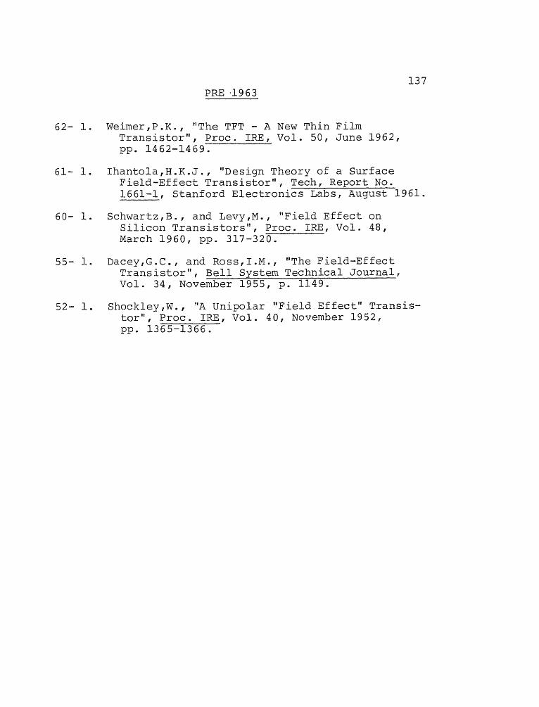
137PRE 1963
62- 1. Weimer,P.K., "The TFT - A New Thin FilmTransistor", Proc. IRE, Vol. 50, June 1962,pp. 1462-1469.
61- 1. Ihantola,H.K.J., "Design Theory of a SurfaceField-Effect Transistor", Tech, Report No. 1661-1, Stanford Electronics Labs, August 1961.
60- 1. Schwartz,B., and Levy,M., "Field Effect onSilicon Transistors", Proc. IRE, Vol. 48,March 1960, pp. 317-320.
55- 1. Dacey,G.C., and Ross,I.M., "The Field-EffectTransistor", Bell System Technical Journal,Vol. 34, November 1955, p. 1149.
52- 1. Shockley,W., "A Unipolar "Field Effect" Transis-tor", Proc. IRE, Vol. 40, November 1952,pp. 1365-1366.