copyright warning &...
TRANSCRIPT

Copyright Warning & Restrictions
The copyright law of the United States (Title 17, United States Code) governs the making of photocopies or other
reproductions of copyrighted material.
Under certain conditions specified in the law, libraries and archives are authorized to furnish a photocopy or other
reproduction. One of these specified conditions is that the photocopy or reproduction is not to be “used for any
purpose other than private study, scholarship, or research.” If a, user makes a request for, or later uses, a photocopy or reproduction for purposes in excess of “fair use” that user
may be liable for copyright infringement,
This institution reserves the right to refuse to accept a copying order if, in its judgment, fulfillment of the order
would involve violation of copyright law.
Please Note: The author retains the copyright while the New Jersey Institute of Technology reserves the right to
distribute this thesis or dissertation
Printing note: If you do not wish to print this page, then select “Pages from: first page # to: last page #” on the print dialog screen
The Van Houten library has removed some of the personal information and all signatures from the approval page and biographical sketches of theses and dissertations in order to protect the identity of NJIT graduates and faculty.

ABSTRACT
EXTENSION TO PV OPTICS TO INCLUDE FRONT ELECTRODE DESIGN IN SOLAR CELLS
by
Debraj Guhabiswas
Proper optical designing of solar cells and modules is of paramount importance
towards achieving high photovoltaic conversion efficiencies. Modeling softwares
such as PV OPTICS, BIRANDY and SUNRAYS have been created to aid such
optical designing of cells and modules; but none of these modeling packages
take the front metal electrode architecture of a solar cell into account
A new model, has been developed to include the front metal electrode
architecture to finished solar cells for optical calculations. This has been
implemented in C++ in order to add a new module to PV OPTICS (NREL’s
photovoltaic modeling tool) to include front metallization patterns for optical
design and simulation of solar cells. This new addition also calculates the
contribution of light that diffuses out of the illuminated (non-metallized) regions to
the solar cell current. It also determines the optical loss caused by the
absorption in the front metal and separates metallic losses due to front and back
contacts. This added capability also performs the following functions:
calculates the total current that can be generated in a solar cell due to optical absorption in each region, including the region beneath the front metal electrodes for the radiation spectrum of AM 1.5,
calculates various losses in the solar cell due to front electrode shading, metal absorption, and reflectance,
makes a plot of how light is absorbed in the metal as well as silicon under the shaded region in the solar cell.
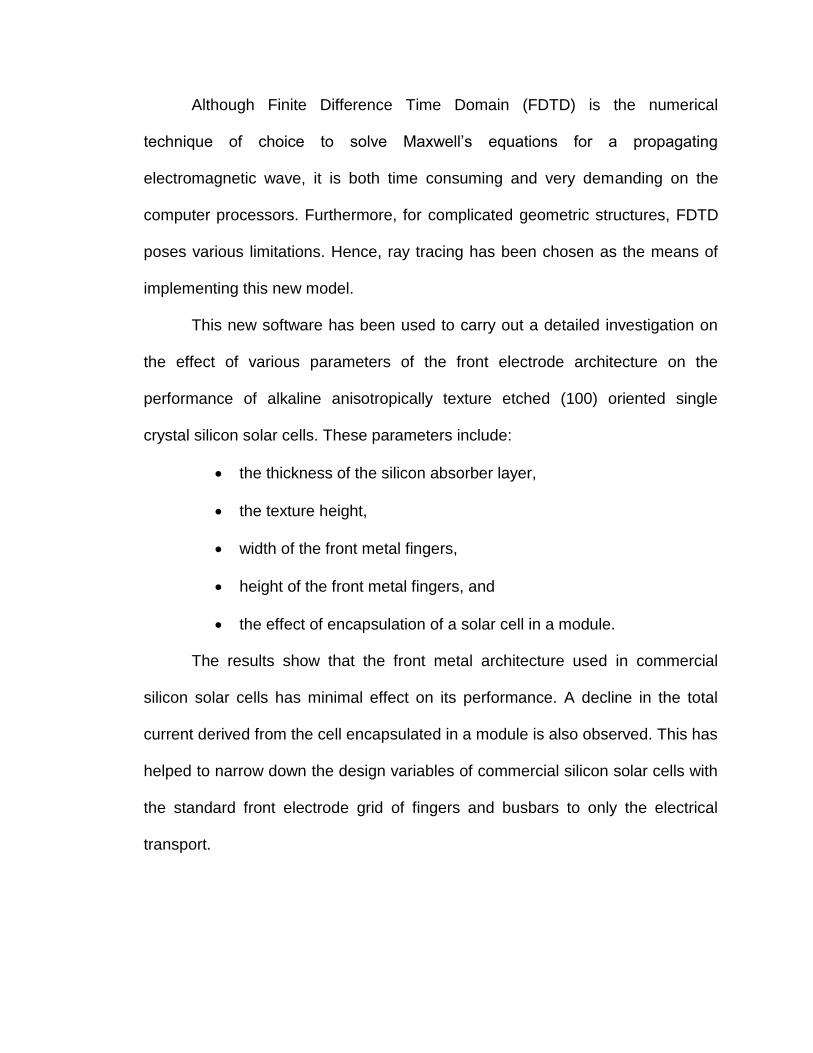
Although Finite Difference Time Domain (FDTD) is the numerical
technique of choice to solve Maxwell’s equations for a propagating
electromagnetic wave, it is both time consuming and very demanding on the
computer processors. Furthermore, for complicated geometric structures, FDTD
poses various limitations. Hence, ray tracing has been chosen as the means of
implementing this new model.
This new software has been used to carry out a detailed investigation on
the effect of various parameters of the front electrode architecture on the
performance of alkaline anisotropically texture etched (100) oriented single
crystal silicon solar cells. These parameters include:
the thickness of the silicon absorber layer,
the texture height,
width of the front metal fingers,
height of the front metal fingers, and
the effect of encapsulation of a solar cell in a module.
The results show that the front metal architecture used in commercial
silicon solar cells has minimal effect on its performance. A decline in the total
current derived from the cell encapsulated in a module is also observed. This has
helped to narrow down the design variables of commercial silicon solar cells with
the standard front electrode grid of fingers and busbars to only the electrical
transport.
EXTENSION TO PV OPTICS TO INCLUDE FRONT ELECTRODE DESIGN IN SOLAR CELLS
by Debraj Guhabiswas
A Dissertation Submitted to the Faculty of
New Jersey Institute of Technology and Rutgers, the State University of New Jersey-Newark
in Partial Fulfillment of the Requirements for the Degree of Doctor of Philosophy in Applied Physics
Federated Department of Physics
January 2013

Copyright © 2013 by Debraj Guhabiswas
ALL RIGHTS RESERVED .

APPROVAL PAGE
Debraj Guhabiswas
Dr. N.M. Ravindra, Dissertation Advisor Date Professor and Chair, Department of Applied Physics, NJIT
Dr. B. Sopori, Dissertation Co-advisor Date Principal Engineer, NCPV, NREL, CO
Dr. Anthony Fiory, Committee Member Date Research Professor of Physics, NJIT
Dr. Tao Zhou, Committee Member Date Associate Professor of Physics, NJIT
Dr. Martin Schaden, Committee Member Date Associate Professor of Physics, Rutgers, Newark
Dr. Ken Ahn, Committee Member Date Assistant Professor in Physics, NJIT
EXTENSION TO PV OPTICS TO INCLUDE FRONT ELECTRODE DESIGN IN SOLAR CELLS

BIOGRAPHICAL SKETCH
Author: Debraj Guhabiswas
Degree: Doctor of Philosophy
Date: January 2013
Undergraduate and Graduate Education:
• Doctor of Philosophy in Applied Physics,New Jersey Institute of Technology and Rutgers, Newark, NJ, 2012
• Master of Science in Material Science and Engineering,New Jersey Institute of Technology, Newark, NJ, 2007
• Bachelor of Engineering in Polymer Science and Chemical Technology,Delhi College of Engineering, New Delhi, India, 2004
Major: Applied Physics
Peer Reviewed Publications
Guhabiswas, D., Sopori, B. A Ray-trace Analysis for Calculating Reflectance ofIndividual Grains and the Total Reflectance of a Textured MulticrystallineSilicon Wafer. (Submitted to EMR)
Guhabiswas, D., Sopori, B., Ravindra, N.M. The Effect of Front ElectrodeArchitecture on the Optical Performance of Silicon Solar Cells . (submittedto Progress in Photovoltaics)
Sopori, B., Guhabiswas, D., Rupnowski, R., Shet, S., Devayajanam, S.,Moutinho, M . An Optical Technique for Measurement of Grain Orientationand Sizes in Multicrystalline Silicon Wafers . (To be submitted Progress inPhotovoltaics)
Conference Presentations/Proceedings
Guhabiswas, D., Sopori, B., Rivero, R., Ravindra, N.M. Extension of PV Optics toinclude front electrode design . Poster Presentation delivered at 22 nd
Workshop on Crystalline Silicon Solar Cells & Modules: Materials andProcesses , Vail, CO, July, 2012.
iv

v
Sopori, B., Guhabiswas, D., Rupnowski, P.; Moutinho, H. New Method for Rapid Measurement of Orientations and Sizes of Grains in Multicrystalline Silicon Wafers. Conference Proceedings, 37th IEEE PVSC ; 2011, page(s) 001680 – 001685. Poster Presentation delivered at IEEE PVSC, Seattle, WA, June 2011.
Sopori, B., Guhabiswas, D., Rupnowski, P., Shet, S., Devayajanam, S., Helio Moutinho, H., and Ravindra, N.M. Rapid measurement of orientations and sizes of grains in multicrystalline silicon wafers: A new technique. Poster presentation delivered at 21st Workshop on Crystalline Silicon Solar Cells & Modules: Materials and Processes, Breckenridge, CO, August, 2011.
Sopori, B., Guhabiswas, D., Rupnowski, P., Shet, S., Devayajanam, S., Helio Moutinho, H., and Ravindra, N.M. Characterization of Grains in Multicrystalline Si Wafers Using an Optical Reflectance Technique. Poster presented at the 2nd MRS workshop on Photovoltaic Materials and Manufacturing Issues II, Denver, CO, October, 2011.
Sopori, B., Sahoo, S., Mehta, V, Guhabiswas, D., Moutinho, H. High Quality Cross-Sectioning Method: Examples of Applications in Optimizing Solar Cell Contact Firing. Conference Proceedings, 37th IEEE PVSC; 2011, page(s) 001674 – 001679. Poster Presentation delivered at IEEE PVSC, Seattle, WA, June 2011.
Sopori, B., Sahoo, S., Mehta, V, Guhabiswas, D., Sean Spiller, S., Helio Moutinho, H.; A method for cross-sectioning large lengths of Solar Cells. 2nd MRS workshop on Photovoltaic Materials and Manufacturing Issues II, Denver, CO, October 2011.
Sopori, B.; Devayajanam, S.; Shet, S.; Guhabiswas, D., Sahoo, S.; Characterizing Damage on Si Wafer Surfaces. 22nd Workshop on Crystalline Silicon Solar Cells & Modules: Materials and Processes, Vail, CO, July, 2012.
Sopori, B.L.; Sahoo, S.; Mehta, V.; Guhabiswas, D.; Spiller, S.; Moutinho, H. Cross-Sectioning Silicon Solar Cell. Poster presented at 21st Workshop on Crystalline Silicon Solar Cells & Modules: Materials and Processes, Breckenridge, CO, August, 2011.
Sopori, B., Rupnowski, P., Guhabiswas, D., Devayajanam, S., Shet, S., Khattak, C. P., Albert, M. (2010). Reflectance Spectroscopy-Based Tool for High-Speed Characterization of Silicon Wafers and Solar Cells in Commercial Production. Conference Proceedings, 35th IEEE PVSC, June, 2010, pp. 002238-002241.
Sopori, B.; Mehta, V.; Guhabiswas, D.; Reedy, R.; Moutinho, H.; To, B.; Shaikh, A.; Rangappan, A. (2009). Formation of a Back Contact by Fire-Through Process of Screen-Printed Si Solar Cells. Conference Proceedings, 34th IEEE PVSC, June, 2009, pp. 001963-001968.
Young, J.L., Mehta, V., Guhabiswas, D., Moutinho, H., Bobby To, Ravindra, N.M., & Sopori, B. (2009 August). Back contact formation in Silicon solar
vi
cells: Investigations using a novel cross-sectioning technique. 19th Workshop on Crystalline Silicon Solar Cells & Modules and Processes, Vail, CO, August, 2009.
Mehta, V., Sopori, B., Guhabiswas, D., Reedy, R., Moutinho, H., To, B., Liu, F., Shaikh, A., Young, H., & Rangappan, A. (2009, August). A new approach to overcome some limitations of back Al contact formation of screen printed silicon solar cells. 19th Workshop on Crystalline Silicon Solar Cells & Modules: Materials and Processes, Vail, CO, August, 2009.
Sopori, B.; Rupnowski, P.; Appel, J.; Guhabiswas, D.; Anderson-Jackson, L. (2009). Light-Induced Passivation of Si by Iodine Ethanol Solution. Materials Research Society Symposium Proceedings, Vol. 1123. Warrendale, PA: Materials Research Society, pp. 137-144

vii
To my beloved family

viii
ACKNOWLEDGMENT
I am deeply grateful to my advisors, Dr. Bhushan Sopori at NREL and Dr. N.M.
Ravindra at NJIT for suggesting and supervising the work presented in this
dissertation. They have been enormously supportive of me throughout the course
of my PhD. I would extend a special thanks to Dr. Bhushan Sopori for sharing his
wide range of knowledge and experience with me during my work at NREL.
This work was supported by the U.S. Department of Energy under
Contract No. DE-AC36-08-GO28308. I am also very grateful to Robert White at
NREL for patiently helping me out with computer programming. Marty Scott at
NREL also deserves a special acknowledgement for teaching me how to use
various optical characterization instruments.
I am especially grateful to my colleagues- Przemyslaw Peter Rupnowski,
Vishal Mehta, Sudhakar Shet, Srinivasmurthy Devayajanam, and Vinay
Budhraja, for all their support at various stages during my stay at NREL.
I benefitted greatly from the advice and insights of the members of my
Dissertation and Oral Examination Committees- Dr. Anthony Fiory, Dr. Tao Zhou,
and Dr. Ken Ahn of NJIT, and Dr. Martin Schaden of Rutgers.
I would like to acknowledge my deepest gratitude towards my family for
supporting me all this while. I owe all this to my dear parents, Mr. Debashish
Guhabiswas and Mrs. Anita Guhabiswas.
Last, but not the least, I would especially like to thank my dear wife, Mrs.
Garima Guhabiswas, for being my greatest support and source of
encouragement.

ix
TABLE OF CONTENTS
Chapter
Page
1
INTRODUCTION…………………………………………………………… 1
1.1 Background…………………………………………………………….
1
1.2 Introduction to Solar Cells……………………………………………
3
1.2.1 Semiconductors……………………………………………….. 4
1.2.2 P-N Junction…………………………………………………… 9
1.2.3 The Solar Spectrum…………………………………………… 13
1.2.4 Solar Cells……………………………………………………… 15
1.3 Introduction to Ray Tracing………………………………………….. 19
1.3.1 Maxwell’s Equations…………………………………………… 20
1.3.2 Plane Waves…………………………………………………… 21
1.3.3 Reflection and Refraction in Non-Absorbing Media……….. 23
1.3.4 Total Reflection………………………………………………… 25
1.3.5 Optics of Absorbing Media…………………………………… 26
1.3.6 Ray Tracing…………………………………………………….. 28
1.4 Dissertation Outline……………………………………………………
29
2
OPTICAL CALCULATIONS AND LIGHT TRAPPING IN SOLAR CELLS: INTRODUCTION AND LITERATURE REVIEW………………
31
2.1 Texturing Based Light Trapping Schemes for Silicon- A Review... 32
2.1.1 Anisotropic Etching of Silicon…………………………………
33
x
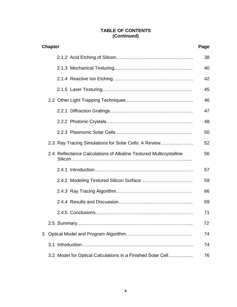
TABLE OF CONTENTS (Continued)
Chapter
Page
2.1.2 Acid Etching of Silicon………………………………………….. 38
2.1.3 Mechanical Texturing………………………………………..…. 40
2.1.4 Reactive Ion Etching……………………………………………. 42
2.1.5 Laser Texturing…………………………………………………. 45
2.2 Other Light Trapping Techniques…………………………………….. 46
2.2.1 Diffraction Gratings……………………………………………... 47
2.2.2 Photonic Crystals……………………………………………….. 48
2.2.3 Plasmonic Solar Cells………………………………………….. 50
2.3 Ray Tracing Simulations for Solar Cells: A Review………………… 52
2.4 Reflectance Calculations of Alkaline Textured Multicrystalline Silicon …………………….……………………………………….........
56
2.4.1 Introduction………………………………………………………. 57
2.4.2 Modeling Textured Silicon Surface …………………………... 59
2.4.3 Ray Tracing Algorithm…………………………………………. 66
2.4.4 Results and Discussion………………………………………… 69
2.4.5 Conclusions……………………………………………………… 71
2.5 Summary………………………………………………………………... 72
3
Optical Model and Program Algorithm……………………………………. 74
3.1 Introduction………………………………………………………………
74
3.2 Model for Optical Calculations in a Finished Solar Cell…………….
76

xi
TABLE OF CONTENTS (Continued)
Chapter
Page
3.2.1 3D Structure Transformation to 2D……………………………
78
3.2.2 Effect of Photon Flux Incident Angle…………………………..
85
3.2.3 Symmetry in the Solar Cell Structure and Computation Regions…………………………………………………………...
87
3.2.4 Integration of Calculations Over the Entire Solar Cell………. 90
3.3 Conclusions……………………………………………………………..
91
4 Summary of Results: Solar Cell…………………………………………….
93
4.1 Introduction……………………………………………………………… 93
4.2 Simulation Results……………………………………………………... 96
4.2.1 Variation in Silicon Absorber Layer Thickness………………. 96
4.2.2 Variation in Metal Finger Width……………………………….. 103
4.2.3 Effect of Texture Height………………………………………... 111
4.3 Conclusions…………………………………………………………….. 115
5
Summary of Results: Solar Cell Encapsulated in Module………………. 116
5.1 Introduction………………………………………………………………
116
5.2 Simulation Results……………………………………………………... 118
5.2.1 Variation in Silicon Absorber Layer Thickness………………. 119
5.2.2 Variation in Metal Finger Width………………………………..
125
5.2.3 Variation in Front Metal Height………………………………... 130
5.3 Conclusion………………………………………………………………
134
xii
TABLE OF CONTENTS (Continued)
Chapter Page
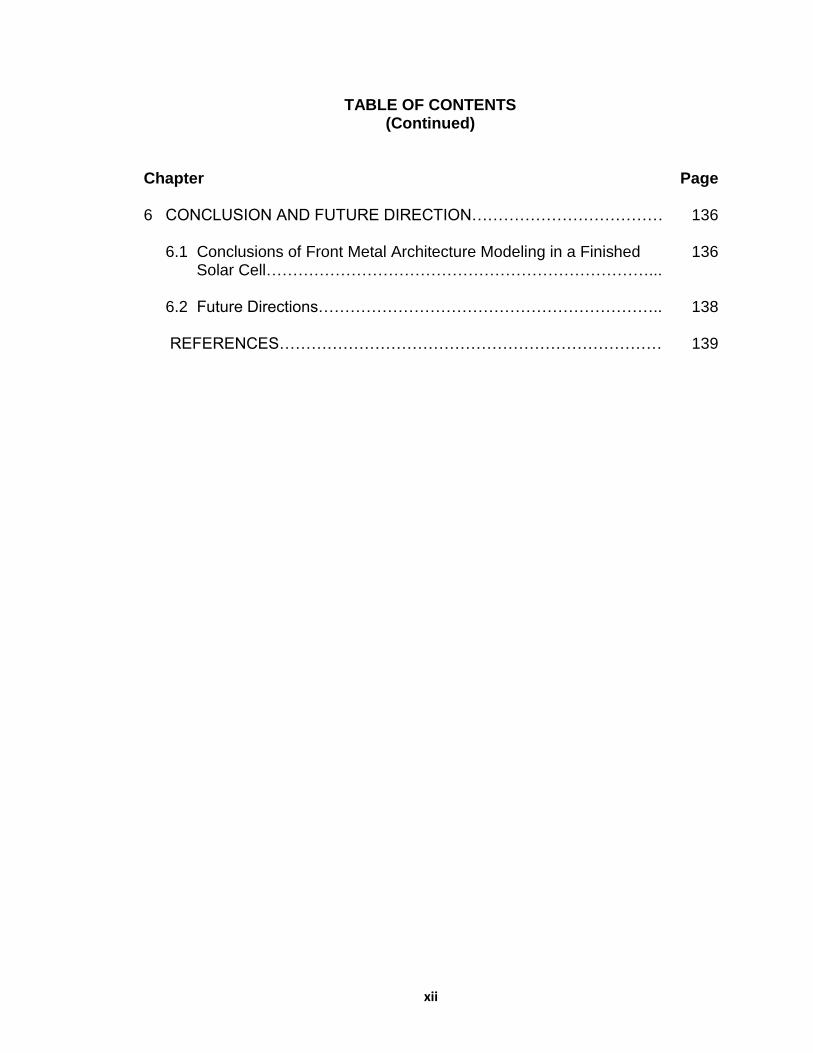
6
CONCLUSION AND FUTURE DIRECTION……………………………… 136
6.1 Conclusions of Front Metal Architecture Modeling in a Finished Solar Cell………………………………………………………………...
136
6.2 Future Directions……………………………………………………….. REFERENCES………………………………………………………………
138
139

xiii
LIST OF TABLES
Table
Page
2.1 θ and φ for some low index crystallographic orientations……………
61
4.1 The various structural parameters of a solar cell that have been maintained constant for calculations..................................................
95
4.2 Parameters kept constant to study the effect of thickness on the performance of a solar cell………………………………………………
97
4.3 Summary of calculated results for different absorber layer thicknesses and metal finger width of 100 µm ……………………….
98
4.4 Summary of calculated results for different absorber layer thicknesses and metal finger width of 75 µm …………………………
107
4.5
Summary of calculated results for different absorber layer thicknesses and metal finger width of 50 µm …………………………
108
4.6
Summary of calculated results for different absorber layer thicknesses and metal finger width of 25 µm …………………………
108
4.7
MAOC values and the percentage current generated in a solar cell with two different texture heights ………………………………………
113
5.1
Properties of glass and encapsulant layers used for simulations….. 118
5.2
Summary of calculated results for different absorber layer thicknesses and metal finger with of 100 µm …………………………
120
5.3
Summary of calculated results for different absorber layer thicknesses and metal finger width of 25 µm …………………………
125
5.4
Summary of calculated results for different absorber layer thicknesses and metal finger width of 50 µm …………………………
126
5.5
Summary of calculated results for different absorber layer thicknesses and metal finger width of 75 µm …………………………
126
5.6 Summary of calculated results for different absorber layer thicknesses and metal finger height of 10 µm ………………………
131
xiv
LIST OF TABLES (Continued)
Table
Page
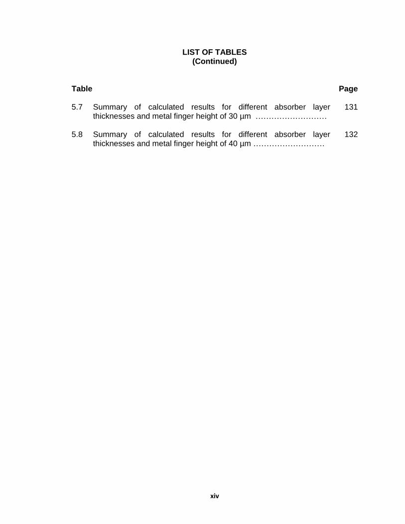
5.7
Summary of calculated results for different absorber layer thicknesses and metal finger height of 30 µm ………………………
131
5.8 Summary of calculated results for different absorber layer thicknesses and metal finger height of 40 µm ………………………
132

xv
LIST OF FIGURES
Figure
Page
1.1
Silicon bond structure an “n-type” dopant Phosphorous and with a “p-type” dopant Boron…………………………………………………..
5
1.2
Band diagram of (a) n-type semiconductor, and (b) p-type semiconductor…………………………………………………………...
6
1.3
Trends of the carrier concentration, the direction of the electric field, and the direction of the drift and diffusion currents for both holes and electrons across an unbiased p-n junction……………….
11
1.4
A p-n junction with the depletion region, carrier concentration across the junction, and the electric field at thermal equilibrium….
12
1.5
Standard J-V curve for an ideal diode………………………………... 13
1.6
Spectral distribution of sunlight for a black body at 6000K, AM 0 and AM 1.5……………………………………………………………….
14
1.7
A standard single junction solar cell structure………………………..
16
1.8
The idealized equivalent circuit of a solar cell………………………..
16
1.9
(a) I-V characteristics curve for a solar cell, (b) the curve in the first quadrant………………………………………………………………….
18
1.10 Oblique view of a 3D plane wave. The blue planes are minima and the red planes are the maxima of the wave amplitude. The black arrow shows the propagation vector of the wave……………………
23
1.11 The refraction and reflection of light at an interface………………...
24
1.12
A rendering of the ray tracing from the eyes of the viewer to the surroundings…………………………………………………………….
29
2.1 The top and angular side view of an SEM image of texture etched (100) silicon wafer surface……………………………………………..
34
2.2 A simulated unit textures on (100) oriented silicon surface…………
35
2.3 Reflection of light from a textured surface and a planar surface......
35

xvi
LIST OF FIGURES (Continued)
Figure Page
2.4 Reflectance for planar and textured silicon. Y-axis is the reflectance X-axis is wavelength of light……………………………...
36
2.5
Unit cell for a diamond crystal lattice, e.g. Silicon…………………… 38
2.6
SEM image of the surface of an acid etched silicon wafer…………. 40
2.7
Standard solar cell made from mechanically grooved multicrystalline silicon…………………………………………………..
41
2.8
Mechanically grooved structures at (a) 35° and (b) 60°……………. 42
2.9
Setup for Reactive Ion Etching………………………………………... 43
2.10
SEM pictures of surface structures on silicon wafers after RIE using (a) SF6/O2~ 1:0.7, (b) SF6/O2~ 1:1, (c) SF6/O2/Cl2 mixture and (d) SF6/O2/Cl2 mixture top view…………………………………..
44
2.11
SEM image of the surface of a laser textured silicon wafer………... 46
2.12
A solar cell design with diffraction grating at the back. ‘p ‘is the period of the grating, ‘si’ is silicon while +1 and -1 are the respective order reflections from the back surface ………………..
48
2.13
Illustration of three solar cell designs: (a) a simple design with a distributed Bragg reflector (DBR), which displays only spectral reflection, (b) a DBR plus a periodically etched grating, displaying spectral reflection and diffraction, and (c) a photonic crystal consisting of a triangular lattice of air holes, displaying simultaneous reflection, diffraction and refraction from the photonic crystal layer. Crystalline silicon is in the light green, low dielectric in light grey and the air is transparent……………………..
50
2.14
A schematic of the plasmonic effect………………………………..... 51
2.15
SEM results and surface reflectance properties of the structure with different densities of Ag nanoparticles on the surface. (a) SEM image of sample with higher particle density. (b) SEM image of sample with smaller particles density. (c) Surface reflectance with different particle densities…………………………………………
52

xvii
LIST OF FIGURES (Continued)
Figure
Page
2.16
Unit cell. In regular textures the ray reenters through a point which is symmetrical to the incident point……………………………………
55
2.17
Random pyramid surface using Rodriguez’s model………………… 56
2.18
The family of eight (111) planes with respect to the X, Y and Z-axes. The eight planes are ABE, ADE, CDE, BCE, ABF, ADF, CDF and BCF. The planes are symmetric about each of the six vertices, A, B, C, D, E and F…………………………………………...
59
2.19
The angles θ and φ for the unit normal to crystallographic plane………………
61
2.20
Part of θ and Φ coordinate system used for calculations. Some low index crystal orientations are marked for reference ……………
62
2.21
(a) Intersection of the family of (111) planes with the (210) crystal plane, (b) top view of unit texture thus formed ………………………
63
2.22
SEM images of textured surfaces on the left (taken from [86]) and calculated periodic surface textures on the right for: a. (100), b. (311) and c. (321) crystal orientations………………………………...
65
2.23
Calculated periodic textures for anisotropically etched a. (211), b. (210) and c. (310) silicon ………………………………………………
66
2.24
The full structure including the sidewalls for periodic boundary condition for a (100) silicon wafer ……………………………………
67
2.25
(A) Calculated reflectance curves for a few alkaline texture-etched low index crystallographic orientation and polished silicon, (B) Reflectance in air for the texture etched wafers (initial thickness ~525 µm) compared to polished 100 µm silicon. (a) (111), (221) & (110), (b) (311) & (210) orientations………………………………….
70
2.26 The reflectance graphs for numerous alkaline texture etched silicon crystal orientations………………………………………………
71
2.27 Flowchart for ray tracing computation……………………………….. 73

xviii
LIST OF FIGURES (Continued)
Figure
Page
3.1 (a) Top view of an array of 2X2 pyramids, (b) side view of the textures…………………………………………………………………...
79
3.2 A 3D image of the front and back sides of an alkaline texture etched (100) silicon substrate………………………………………….
79
3.3 The standard structure 2D used for calculations…………………….
80
3.4
(a) The standard structure used for calculations (marked in blue dashed lines in Figure 3.3), and (b) deduction of this structure from 3D…………………………………………………………………...
80
3.5
The front electrode architecture of a standard solar cell…………… 82
3.6
The 2D cross-sectional construction of fingers on textured silicon substrate………………………………………………………………….
83
3.7
2D cross-sectional rendering of a busbar for the complete device structure…………………………………………………………………..
84
3.8
The pyramidal texture on (100) silicon surface. Note the pair of blue and black lines denoting the plane of propagation of reflected and transmitted light…………………………………………………….
84
3.9
The incident photon flux at an angle with respect to the vertical (Y-axis)……………………………………………………………………
86
3.10
2D structure of the cross-section of a finished solar cell with no front metal. The blue arrows denote the incident rays while the red arrows denote the transmitted rays……………………………………
88
3.12
The region perpendicular to the metal fingers. ‘dF’ is the region in between two metal fingers……………………...................................
89
3.13
The top view of the meshing of a solar cell with a few pyramids shown for reference……………………………………………………..
91
4.1
The interaction of normally incident light with front metal………….. 96

xix
LIST OF FIGURES
(Continued)
Chapter
Page
4.2 Plot of MAOC with respect to silicon thickness………………………
99
4.3
Plots of Reflectance Loss and Back Metal Loss with respect to silicon thickness…………………………………………………………
99
4.4
Plot of percentage current generated in the shaded region……….. 100
4.5
Optical absorption under the busbar in (a) Silicon, (b) Back Metal, and (c) Front Metal for silicon thickness of 40 µm plotted in log scale………………………………………………………………………
104
4.6
Optical absorption under a metal finger in (a) Silicon, (b) Back Metal, and (c) Front Metal for silicon thickness of 40 µm…………...
105
4.7
Plot of MAOC values with respect to silicon thickness for metal finger width of (a) 100 µm, (b) 75 µm, (c) 50 µm, and (d) 25 µm…..
109
4.8
Plot of back metal loss with respect to silicon thickness for metal finger width of (a) 100 µm, (b) 75 µm, (c) 50 µm, and (d) 25 µm…..
109
4.9
Plot of reflectance loss with respect to silicon thickness for metal finger width of (a) 100 µm, (b) 75 µm, (c) 50 µm, and (d) 25 µm…..
110
4.10
Plot of percentage current generated in the shaded region for various silicon absorber layer thickness and front metal contact width………………............................................................................
111
4.11
The 2D cross-sectional structure of a textured (100) silicon solar cell without front metal electrode. The texture height is marked for reference…………………………………………………………………..
112
4.12
Comparison of MAOC values for solar cells with texture height 3 µm and 2 µm……………………………………………………………...
114
4.13
Comparison between the current generated in the shaded region for solar cells with texture height 3 µm and 2 µm……………………..
114
5.1
The various constituents of a solar module and a solar panel……… 117

xx
LIST OF FIGURES
(Continued)
Chapter
Page
5.2
Optical effects in a module……………………………………………... 117
5.3
Plot of MAOC of (a) cell, and (b) module with respect to silicon thickness…………………………………………………………………..
120
5.4 Plots of Reflectance Losses for (a) cell, and (b) module…………….
121
5.5
Plots of Back Metal Losses for (a) cell, and (b) module…………….. 121
5.6
Plot of percentage current generated in the shaded region………… 122
5.7
Absorption under busbar in (a) Silicon, (b) Back Metal, and (c) Front Metal for a module with a 40 µm thick silicon absorber layer...
123
5.8
Absorption under a finger in (a) Silicon, (b) Back Metal, and (c) Front Metal for a module with a 40 µm thick silicon absorber layer...
124
5.9
Plot of MAOC values for module with respect to silicon thickness for metal finger width of (a) 100 µm, (b) 75 µm, (c) 50 µm, and (d) 25 µm………………………………………………………………………
127
5.10
Plot of reflectance loss values for module with respect to silicon thickness for metal finger width of (a) 100 µm, (b) 75 µm, (c) 50 µm, and (d) 25 µm………………………………………………………..
127
5.11
Plot of reflectance loss values for module with respect to silicon thickness for metal finger width of (a) 100 µm, (b) 75 µm, (c) 50 µm, and (d) 25 µm………………………………………………………..
127
5.12
Plot of percentage current produced in shaded region for module with respect to silicon thickness for metal finger width of (a) 100 µm, (b) 75 µm, (c) 50 µm, and (d) 25 µm……………………………..
128
5.13
Plot of MAOC values for cell and module with respect to silicon thickness for metal finger width of (a) 100 µm, (b) 75 µm, (c) 50 µm, and (d) 25 µm…
128

xxi
LIST OF FIGURES
(Continued)
Chapter
Page
5.14
Plot of reflectance loss for cell and module with respect to silicon thickness for metal finger width of (a) 100 µm, (b) 75 µm, (c) 50 µm, and (d) 25 µm............................................................................
129
5.15
Effect of metal height on module optics……………………………… 130
5.16 MAOC plots for metal height thicknesses of (a) 10 µm, (b) 20 µm, (c) 30 µm, and (d) 40 µm……………………………………………….
132
5.17
Reflectance loss plots for metal height thicknesses of (a) 10 µm, (b) 20 µm, (c) 30 µm, and (d) 40 µm…………………………………..
133
5.18
Back metal loss plots for metal height thicknesses of (a) 10 µm, (b) 20 µm, (c) 30 µm, and (d) 40 µm…………………………………..
133
5.19
Percentage current generated in the shaded region of a module plots for metal height thicknesses of (a) 10 µm, (b) 20 µm, (c) 30 µm, and (d) 40 µm............................................................................
134

1
CHAPTER 1
INTRODUCTION
1.1 Background
Can you imagine a world without energy? Each and every scientific and
technological development that helps us to improve our standard of living, to
connect to people around us via smart-phones or do the most basic things in our
lives such as travelling would be meaningless if we did not have the energy to
make it work. At present, the staple sources of energy for mankind are fossil
fuels. We burn fossil fuels to drive our cars, to generate electricity and to do
every thing that requires energy. The major side effect of burning such huge
amounts of fossil fuels each day is the exhaust of many harmful gases such as
carbon dioxide, carbon monoxide, sulphur oxides etc. into the earth’s
atmosphere. These man-made additions to our atmosphere have led to air
pollution and global warming. It is common knowledge that global warming, over
the period of next many years, will have catastrophic effects on our ecosystems.
This, along with the fact that fossil fuels will not last forever, makes it imperative
for us to look for clean and renewable sources of energy and technologies to
harness them efficiently.
The Sun contains the largest reservoir of energy that can be used by
mankind. It is abundant, freely available and renewable in nature. The interaction
of light with matter has long been studied with enormous interest. Becquerel, in
1839, first reported the photovoltaic effect when he observed an increase in the

2
electricity generation rate in an electrolytic cell made up of two metal electrodes
placed in an electrically conducting solution upon exposure to light. Willoughby
Smith discovered photoconductivity of selenium in 1873. William Grylls Adams
and Richard Evans Day, in 1876, were the first to discover that selenium
produced electricity when exposed to light while an American inventor, Charles
Fritts, described the first solar cells made out of selenium wafers in 1883. In
1887, Heinrich Hertz observed that ultraviolet light altered the lowest voltage
capable of causing a spark to jump between two metal electrodes. Albert Einstein
first proposed the photoelectric effect in 1905, which was experimentally verified
later by Robert Millikan in 1916. 1932 was a defining period when Audobert and
Stora discovered the photovoltaic effect in cadmium sulfide (CdS). The first
silicon solar cell was reported in 1941; but it was only in 1954 when Daryl
Chapin, Calvin Fuller, and Gerald Pearson, at Bell Labs, developed the
forerunner of the present silicon solar cells. Since then, the use of solar cells has
expanded from space to terrestrial applications. All this has been accompanied
by a huge reduction in the manufacturing cost of commercial solar cells. The
complete timeline on the discoveries and developments relating to solar energy
can be found at the US Department of Energy’s website cited in reference [1]
while a comprehensive history on the development of solar cells can be found in
reference [2].
The ability to utilize the energy from the Sun is the key to the future well-
being of mankind. In this respect, the solar cell is considered to be the most

3
promising technology that can help use this form of energy efficiently and in a
meaningful manner. Hence, it is essential that a brief introduction to the physics
of semiconductors and the p-n junction in both dark and illuminated conditions be
discussed. This will lead to a much better understanding of the technology of
solar cells. A brief introduction to the fundamentals of optics used in this work
including ray-tracing will be provided in this chapter to facilitate a better
understanding of the model developed in this dissertation.
1.2 Introduction to Solar Cells
A brief introduction to the functioning of solar cells will be given in this section. In
order to highlight the concepts of photovoltaics used in this dissertation, this
section will be broken up into the following sub-sections:
1) Semiconductors
2) P-N Junction
3) The Solar Spectrum
4) Solar Cells: Functioning and Structure
The first topic will give an overview of the physics of the building block of solar
cells: semiconductors. Basically, a solar cell is a large area diode with metal
contacts at both ends to extract the photo-generated carriers that flow due to a
concentration gradient within it. The second topic will focus on a basic
explanation of a p-n junction, without which there would be no solar photovoltaic
technology. The third topic will outline the characteristics of the solar irradiance
received on earth. This is most vital since all the optical modeling in this

4
dissertation is based on the solar irradiance. The fourth topic will enunciate the
functioning of solar cells along with a brief description of the structure of a
standard crystalline solar cell that has been used for calculations in this thesis.
For those interested in other technologies as well, relevant references to review
articles pertaining to those topics will be provided for further reading.
1.2.1 Semiconductors
Solid-state materials are classified into three groups according to their electrical
properties- insulators, semiconductors, and conductors. Insulators are materials
that have very low conductivities while conductors are materials that have very
high conductivities. Semiconductors are materials that have conductivities in
between those of insulators and conductors. It is important to note that the
conductivity of a semiconductor is generally sensitive to illumination, impurities,
and magnetic field. This sensitivity of the conductivity of a semiconductor to
illumination and impurities is exploited in a solar cell through what is called as the
photovoltaic effect.
Semiconductors can be elements, e.g. silicon and germanium, as well as
compounds, e.g. GaAs, CdTe, CdS etc. in nature. Such pure semiconductors are
also called intrinsic semiconductors. When impurities, also called dopants, are
added to a semiconductor, they introduce excess electrons or holes in the crystal
lattice. For example, Group V elements from the periodic table, such as
phosphorus or arsenic are added to silicon, silicon behaves as an “n-type”
semiconductor with electrons being the majority charge carriers. Introduction of
impurities that makes a semiconductor deficient in electrons, e.g. Group III

5
elements from the periodic table such as boron, aluminum or gallium in silicon,
makes it “p-type” with “holes” being the majority carriers. Such semiconductors
are also called extrinsic semiconductors. Extrinsic or doped semiconductors have
much larger conductivity compared to the intrinsic semiconductors. Their
conductivity is proportional to the concentration of impurities in it. Doping plays
an essential role in all semiconductor devices.
Figure 1.1 shows the bond diagram of silicon lattice with an n-type dopant,
and a p-type dopant. Note the valence electrons in the yellow regions and the
dopant-introduced conduction electron outside of that region in the n-type silicon
doped with phosphorous in Figure 1.1, and the dopant-introduced mobile hole in
the p-type silicon doped with boron in the same Figure. Both of them, being more
mobile than the valence electrons, conduct more easily. A band structure
diagram, shown in Figure 1.2, can also represent the bond structure shown
below.
Figure 1.1 Silicon bond structure with an “n-type” dopant phosphorous and with a “p-type” dopant boron [3].

6
Figure 1.2 shows a simplified band diagram of intrinsic, n-type and p-type
silicon. The electrons bound to the silicon atom lie in the valence band while the
conduction electrons lie in the conduction band with Eg, the “Band Gap” between
the valence band and the conduction band, being the “Forbidden Region”
because no electrons can occupy these energy states. In the case of an undoped
or intrinsic semiconductor, there is just the right number of electrons to fill the
valence band completely. It is only when some of the valence band electrons are
excited to the conduction band, due to thermal or optical excitation, that the
semiconductor can start to conduct electricity. As can also be seen from Figure
1.2, introduction of impurities changes the effective gap between the conduction
band and the valence band due to the introduction of a new Donor Level (Ec), the
energy level of an n-type dopant, and the Acceptor Level (Ev), the energy level of
a p-type dopant. This is of vital importance to not only to the functioning of solar
cells but all semiconductor devices.
Figure 1.2 Band diagram (a) n-type semiconductor, and (b) p-type semiconductor [4].

7
The electron carrier density in an extrinsic semiconductor is given by:
⁄ (1.1)
and similarly, the hole carrier density in an extrinsic semiconductor is given by
⁄ (1.2)
where n is the electron density, p is the hole density, EF is the intrinsic Fermi
level, NC and NV are constants at fixed T known as the effective density of states
in the conduction band and the effective density of states in the valence band,
respectively, k is the Boltzmann constant and T is the temperature of the
semiconductor in Kelvin.
The electron density, n, and the hole density, p, are related to each other
in terms of the intrinsic carrier concentration, ni, by:
(1.3)
The resistivity and conductivity of a semiconductor is given by:
( ) (1.4)
8
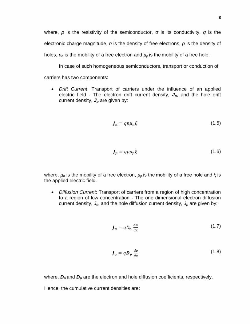
where, ρ is the resistivity of the semiconductor, σ is its conductivity, q is the
electronic charge magnitude, n is the density of free electrons, p is the density of
holes, µn is the mobility of a free electron and µp is the mobility of a free hole.
In case of such homogeneous semiconductors, transport or conduction of
carriers has two components:
Drift Current: Transport of carriers under the influence of an applied electric field - The electron drift current density, Jn, and the hole drift current density, Jp are given by:
(1.5)
(1.6)
where, µn is the mobility of a free electron, µp is the mobility of a free hole and ξ is the applied electric field.
Diffusion Current: Transport of carriers from a region of high concentration to a region of low concentration - The one dimensional electron diffusion current density, Jn, and the hole diffusion current density, Jp are given by:
(1.7)
(1.8)
where, Dn and Dp are the electron and hole diffusion coefficients, respectively.
Hence, the cumulative current densities are:

9
(1.9)
(1.10)
(1.11)
where, Jtot is the total conduction current density.
The continuity equations for minority carriers are:
(1.12)
where, G is the generation rate while R is the recombination rate. A rigorous
solution of these equations can be achieved throughout the semiconductor
sample.
1.2.2 pn Junction
A pn junction results when a p-type semiconductor is doped with an n-type
impurity or vice versa. Due to carrier concentration gradients between both the
sides, excess electrons from the n-type side flow into the p-type side while
excess holes from the p-type side flow into the n-type side, giving rise to the
diffusion component of the current density. This migration of charges leaves
behind charged ion cores near the junction of both the semiconductors creating
the pn junction. The charged ion cores give rise to an electric field directed from

10
the n-doped region to the p-doped region, which in turn creates the drift
component of the current. The charged region at the junction, also called the
space charge region, is deficient in free carriers. At equilibrium, the drift current
exactly cancels out the diffused current. Solving the continuity equations along
with the Poisson equation for the material gives the thickness of the pn junction
and the built-in voltage. The Poisson’s equation is:
(1.13)
where, εs is the relative permittivity of the medium.
The built-in potential (Vbi) due to the space charge region is given by:
(
) (1.14)
where, NA is the acceptor dopant concentration and ND is the donor dopant
concentration.
The width of an abrupt pn junction width is given by:
√
(
)
(1.15)
The formation of the pn junction is also accompanied by the bending of
the valence and conduction energy bands near the junction. This bending is

11
proportional to the electric field across the pn junction. Figure 1.3 shows the
direction of the electric field, the direction of the drift and diffusion currents for
holes and electrons, the band bending and other details across an unbiased pn
junction.
Figure 1.3 Trends of the carrier concentration, the direction of the electric field, and the direction of the drift and diffusion currents for both holes and electrons across an unbiased pn junction [5].
Figure 1.4 shows the effect of biasing on the bending of valence and
conduction bands. In the Figure, VJ is the junction voltage and V is the applied
voltage. The insets at the bottom also show the circuits for reverse and forward
biasing. As can be seen, the depletion region increases during reverse biasing
and it decreases during forward biasing.
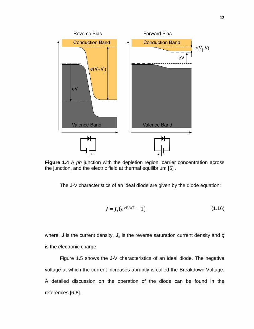
12
Figure 1.4 A pn junction with the depletion region, carrier concentration across the junction, and the electric field at thermal equilibrium [5] .
The J-V characteristics of an ideal diode are given by the diode equation:
( ⁄ ) (1.16)
where, J is the current density, Js is the reverse saturation current density and q
is the electronic charge.
Figure 1.5 shows the J-V characteristics of an ideal diode. The negative
voltage at which the current increases abruptly is called the Breakdown Voltage.
A detailed discussion on the operation of the diode can be found in the
references [6-8].

13
Figure 1.5 Standard J-V curve for an ideal diode [9].
1.2.3 The Solar Spectrum
The effective temperature on the surface of the Sun is 5778 K [10]. Figure 1.6
shows the radiation spectrum expected from a black body at 6000 K. The
incident radiant power from the Sun, perpendicular to its direction, per unit area,
outside the earth’s atmosphere is constant for all practical purposes. This
radiation intensity was measured to be 1.353 kW/m2 [11] and is called air mass
zero (AM0) radiation. As can be seen from Figure 1.6, the incident radiation from
the sun is different from that of a black body at 6000K. This is attributed to the
effects such as differing transmissivity of the sun’s atmosphere at various
wavelengths [12].
The radiation reaching the surface of the earth is reduced by more than
30% while travelling through the earth’s atmosphere. This attenuation is due to
Rayleigh scattering, scattering by aerosols and dust particles and absorption by

14
the atmosphere and its constituent gases [13, 14]. The total incident power
reaching any point on the earth, at a given time under clear conditions, is
dependent on the length of the light path through the atmosphere.
Figure 1.6 Spectral distribution of sunlight for a black body at 6000K, AM 0 and AM 1.5 [15].
The ratio of the actual path length to the minimum, i.e., when the sun is
directly overhead, is called the optical air mass. Hence, when the sun is directly
overhead, the optical air mass is 1. This is also denoted as air mass one (AM 1)
radiation. This is written mathematically as:
(1.17)
where, θ is the angle of the sun with the vertical overhead.

15
This implies that, with increasing air mass but keeping all the other
variables constant, the incident radiation decreases as the air mass increases.
The most commonly used air mass for solar cell calculations and characterization
is AM 1.5. In 1977, the U.S. government’s photovoltaic program standardized this
to a total power density of 1 kW/m2 [16]. The ideal solar cell efficiencies at 300 K
have also been calculated as a function of energy bandgap under one sun AM
1.5 irradiance [17]. Hence, all calculations in this dissertation have been done for
an irradiance of AM 1.5.
1.2.4 Solar Cells
A solar cell is a semiconductor device that converts sunlight directly to electricity.
It has the potential to provide power nearly permanently with low operating costs
and create almost no pollution at all [18, 19]. Even though silicon solar cells have
been the workhorse of the photovoltaic industry over the last many decades,
other materials and technologies have also become relevant now [20-31].
The simplest design for a solar cell consists of a single shallow pn junction
on the surface, a front ohmic contact stripe and fingers, a back ohmic contact
covering the entire back surface, and an antireflection coating on the front [32] as
shown in Figure 1.7. When a solar cell is illuminated with light, photons with
energy higher than the band gap, Eg, are absorbed producing an electron-hole
pair while photons with energy less than the band gap are not absorbed, thereby,
making no contribution to the output current.
The output of a solar cell can be approximated using the one diode model.
Figure 1.8 shows this circuit where IL is the source current resulting from the

16
excitation of excess carriers by solar radiation, Is is the diode saturation current,
and RL is the load resistance. This model can be made more complicated for
better approximation. But the one diode model has proven to be quite
satisfactory.
Figure 1.7 A standard single junction silicon solar cell structure [33].
Figure 1.8 The idealized equivalent circuit of a solar cell.

17
The ideal I-V characteristics of such a single junction solar cell is given by:
( ⁄ ) (1.18)
(
√
√
) ⁄
(1.19)
(1.20)
where, A is the device area, Dn and Dp are the diffusivities of electron and hole in
p and n-type regions respectively, Le and Lh are the minority carrier diffusion
length in the p and n-type regions respectively and W is the depletion region
width.
During the functioning of a solar cell, the I-V curve passes through the
fourth quadrant allowing power to be extracted from the device. Generally, this
curve is inverted and represented in the first quadrant. Figure 1.9(a) shows the
general I-V curve for a solar cell and Figure 1.9(b) shows the inverted curve in
the first quadrant. From Figure 1.9, the yellow triangle shows the maximum
power (Pmax) rectangle of a solar cell.
(1.21)

18
(a) (b)
Figure 1.9 (a) I-V characteristics for a solar cell [34], (b) the curve in the first quadrant [35].
The I-V curve provides important parameters about a solar cell that have a
significant effect on its performance.
Open Circuit Voltage (Voc): This is the voltage across a solar cell when I=0. Its expression can be evaluated from Eq. 1.18 by equating IL=0. As can be seen from the equation above, Voc is inversely proportional to IS.
(
) (1.22)
Short Circuit Current (ISC): This is the current across the solar cell at zero voltage. The short circuit current depends on the minority carrier lifetimes and the total number of photo-generated carriers in the cell.
Fill Factor (FF): The higher the fill factor of a solar cell, the higher is its efficiency. The fill factor of a solar cell can be calculated by the following formula:

19
(1.23)
Efficiency of energy conversion (η):
(1.24)
where, Pin is the incident optical power on the solar cell. As can be seen from Eq.
(1.24), the higher the short circuit current (ISC) and the open circuit voltage VOC,
the higher is the efficiency of the solar cell. Other than the above-mentioned
parameters, two types of resistances: series (RS) and shunt (RSH) are also
important parameters affecting the performance of a solar cell. A thorough
discussion on the topic of solar cells can be found in reference [36].
1.3 Introduction to Ray-Tracing
Ray-tracing is the solution of Maxwell’s equations for the propagation of an
electromagnetic wave within the regime of geometrical optics, i.e., the
wavelength of the incident ray is much smaller than the object dimensions. The
following is a brief introduction to the relevant optics. This includes optics of non-
absorbing media, absorbing media, the concept of total reflection and an
introduction to 3- dimensional plane waves.

20
1.3.1 Maxwell’s Equations
Maxwell’s equations form the backbone of electrodynamics as well of optics. This
calls for a brief review of these equations and their significance. The Maxwell’s
equations, in SI units, are given by [37]:
(1.25)
(1.26)
(1.27)
(1.28)
where, j is the electric current density, D is the electric displacement, E is the
electric field, B is the magnetic induction, and H is the magnetic vector.
These variables are further related to each other by:
(1.29)
(1.30)

21
(1.31)
where, σ is the specific conductivity, ε is the dielectric constant or permittivity and
µ is the magnetic permeability. In a homogeneous medium, the Maxwell’s
equations reduce to [38]:
(1.32)
(1.33)
Eq. (1.32) and Eq. (1.33) are standard equations of a wave travelling with a
velocity:
√ ⁄ (1.34)
Optical waves are also governed by the same set of equations. The wave that
has the least complicated field evolution pattern is a plane wave.
1.3.2 Plane Waves
If V(r, t) to represents each rectangular component of the field vectors in a
region free of currents and charges, the solution to the Maxwell’s field equations
yield the following wave equation [39]:

22
0 (1.35)
The simplest solution to the above equation of the form is a plane
wave because at each instant of time, V is a constant over each of the planes
and
r . s=constant (1.36)
where, r is the position vector of the point in consideration and s is the unit vector
in the direction of propagation of the wave. The solution to Eq. (1.35) yields [39]:
(1.37)
where, V1 and V2 are arbitrary functions. V1 represents a disturbance travelling in
the positive direction while V2 represents a disturbance travelling in the negative
direction. The solution to Eq. (1.35), for E and H, yields:
E=E0 (r.s-vt) and H=H0 (r.s-vt) (1.38)
The solution of the Maxwell’s field equations with the above expressions for E
and H and setting ⁄ √ ⁄ results in:

23
√
, √
(1.39)
On closer inspection, it is found that E.s = H.s = 0 implying that the fields
in this case are transversal in nature, i.e., electric and magnetic field vectors lie in
planes normal to the direction of propagation. Fig 1.10 shows a graphical
representation of a travelling 3D plane wave. The blue planes are the minima
positions and red planes are the maxima positions of the amplitude of the plane
wave. All the points on each plane have the same amplitude and propagation
direction.
Figure 1.10 Oblique view of a 3D plane wave. The blue planes are minima and the red planes are the maxima of the wave amplitude. The black arrow shows the propagation vector of the wave [40].
1.3.3 Reflection and Refraction in Non-Absorbing Media On solving the plane wave equations at the boundary between two media with
different but real refractive indices gives [41]:

24
√
(1.40)
(1.41)
Eq. (1.40) is the law of refraction and Eq. (1.41) is the law of reflection, also
called Snell’s law, of light at a surface. Figure 1.11 shows the refraction of light
from one medium to the other.
Figure 1.11 The refraction and reflection of light at an interface [42].
Similarly, solving the wave equations at the boundary gives the reflection
and transmission coefficient of the wave, also called the Fresnel formulae [43]:
(1.42)

25
(1.43)
⁄ (1.44)
(1.45)
(1.46)
⁄ (1.47)
(1.48)
where, R is the reflection coefficient, T is the transmission coefficient, AS is the
amplitude component perpendicular to the propagation direction and AP is the
amplitude component in the parallel direction. The amplitude can be complex.
1.3.4 Total Reflection
The condition for total reflection can be deduced from the Snell’s law [44]. When
a wave is moving from an optically denser medium to an optically rarer medium,
i.e., from Figure 1.11:

26
√
(1.49)
If the sine of angle of refraction becomes more than 1, there is no transmittance
and all the light is reflected back.
1.3.5 Optics of Absorbing Media
Till now, the propagation of a light wave in a non-absorbing medium has been
discussed. It would be very pertinent to look at the case in which the medium is
absorbing. In this case, Eq. (1.25) from the Maxwell’s field equations can be
written as [45]:
(1.50)
The wave equation for this case then becomes:
(1.51)
where, the second term on the right hand side implies a damped wave suffering
progressive attenuation. On taking E and H of the form and
, Eq. (1.51) becomes [46]:
(1.52)

27
In the above equation, is complex. It is given by:
(
)
(1.53)
The dielectric constant, ε, in the above equation is the same as in the case
of non-absorbing media. But for the case of absorbing media, Eq. (1.53) is
replaced by:
(1.54)
√ ,
√
(1.55)
The refractive index, in this case, becomes [46]:
(1.56)
where ‘k’ is the extinction coefficient. The loss in the intensity of a plane wave in
an absorbing medium is given by:
(1.57)

28
where,
is the absorption coefficient. The reflection coefficient now
becomes [47]:
(1.58)
(1.59)
Whenever a highly absorbing medium such as a metal is encountered by a plane
wave, the above-mentioned equations are used.
1.3.6 Ray Tracing
The equations given in the preceding sections lay the foundations for ray-tracing
simulations. Although ray tracing is mainly used for rendering computer graphics
[48] and lens design [49], it has been used in solar cell calculations as well [50].
Figure 1.12 shows a schematic of the ray-tracing process. The tracking and
labeling of the rays should be noted.
In this scheme of calculations, the incident optical wave is denoted by a
large number of rays travelling in the same direction as the propagation vector
and with the same intensity as that of the plane wave around that location. Each
incident ray has a relative intensity of 1.0 at the start of the calculation. As these
rays progress in space, they are tracked till their intensity is all absorbed or if
they are captured by one of the detectors. The reflection and transmission
coefficients are calculated at each interface in the path of the wave. The intensity

29
of the wave is updated at each interface and while it is absorbed. ‘Daughter rays’
are created each time a ray splits up into the reflected and the transmitted ray.
Once all the rays have travelled their respective paths, the accumulated
intensities for absorption, reflection and transmission are integrated and
averaged over the entire spatial area of the calculations and over the entire
wavelength range. The complications of ray tracing are not only limited to the
optical effects but also include the geometric and material features of the region
of interest.
Figure 1.12 A rendering of the ray tracing from the eyes of the viewer to the surroundings. The state of the ray is updated all along till it is completely absorbed or captured [51].
1.4 DISSERTATION OUTLINE
Optical modeling of solar cells and modules is a very important process in
optimizing cell efficiency by adjusting the cell architecture, and finding a
compromise between efficiency and the production cost. Till now, all the
softwares commercially available do not have the option to include front metal

30
electrode architecture during optical modeling. Due to this, no thorough
investigations have been carried out to ascertain the effect of the front metal
architecture on the optical performance of solar cells. This work has been
successful in:
Developing a new model to incorporate front metal structure under the purview of ray-tracing,
Developing a new algorithm to incorporate into a software program,
Writing a new code in C++ to handle these complex calculations, and
Carrying out a detailed investigation into the effect of front metal architecture on the optical performance of solar cells.
The dissertation consists of a total six chapters. It will be organized as follows:
The second chapter will present a review of the work done in this field till now and the approach taken by various groups.
The third chapter will present the model and algorithm used in this work in detail.
The fourth chapter will present the results for calculations done on single crystal, anisotropic texture etched, single junction and commercial silicon solar cells.
The fifth chapter will present the results for calculations done with these cells encapsulated in a complete module and outline the effect of encapsulation on solar cells.
The sixth chapter will outline the conclusions and future direction of work.

31
CHAPTER 2
OPTICAL CALCULATIONS AND LIGHT TRAPPING IN SOLAR CELLS:
INTRODUCTION AND REVIEW
Optical calculations for solar cells, FDTD [52] or ray tracing [53], are done to
examine their light trapping characteristics [54-56]. Since solar Cells work by
capturing a part of the radiation incident on them and converting them to
electricity, it means that any technology which helps a solar cell to increase the
amount of light it captures would in turn increase the amount of power that we
derive from it. The process of confining as much light as possible in a solar cell is
termed as Light Trapping. The first suggestion of using light trapping by total
internal reflection to increase the effective absorption in crystalline silicon were
motivated by the prospect of increasing the response speed of silicon
photodiodes while maintaining high quantum efficiency in the near infrared region
[57, 58]. Many different techniques have been tried to make light trapping as
efficient as possible. This chapter will present an overview of the various light
trapping schemes that have been tried and adopted in the field of solar cells. The
review will only focus on silicon based solar cell devices and will not digress into
other material based technologies as that is not the focus of this dissertation.
As will be seen during the review of various light trapping schemes in
silicon solar cells, surface roughening is a very important method of reducing the
reflectance of light and increasing absorption in a solar cell. Hence, the first
section of this chapter will present a review of the many methods used to

32
artificially roughen the surface of silicon wafers or films, also called Texturing.
These methods include chemical texturing process as well as laser texturing
processes. The second part of this chapter will be based on light trapping
schemes that are not based on the texturing of the silicon substrate.
The last part of this chapter will be a review of the methodologies used in
ray tracing calculations for solar cells and their results. The main reason for
performing ray-tracing calculations is to understand the efficiency of light trapping
schemes and the various optical losses taking place in a solar cell. They are also
used to optimize the design and architecture of not just a solar cell but also of a
complete module. This section will also investigate the various ray tracing optical
modeling softwares presently available to specifically model solar cells. Lastly, a
new method to calculate the reflectance of a potassium hydroxide etched
complete multi-crystalline silicon wafer will be explained. This work was done by
Guhabiswas during the course of his doctoral work and has led to the
development of a new and ultra-fast grain orientation characterization technique
[59].
2.1 Texturing Based Light Trapping Schemes for Silicon: A Review
It has been shown that texturization can increase the short circuit current in a
solar cell due to three main reasons [60] :
By reduction in reflectance of the solar cell,
Light trapping in the volume of the device,

33
Higher light absorption closer to the junction in comparison to a planar
surface.
Hence, texturing of silicon has become an inseparable part of silicon solar cell
manufacturing [61-67]. Following are the texturing processes that will be
reviewed in this chapter:
Anisotropic Etching
Acid Etching
Mechanical Texturing
Reactive Ion Etching
Laser Etching
2.1.1 Anisotropic Etching of Silicon
Even though wet chemical isotropic etching has been used in the silicon
semiconductor industry during processing since the 1950’s [68, 69], it took a little
while longer for anisotropic etching of silicon to follow suit [70, 71]. But it was only
during the mid-1970’s that this process was first introduced for silicon solar cell
processing [72].
The anisotropic etching process of silicon is orientation dependent, i.e.,
different crystal orientations have different etch rates. The most common
chemical used for this is potassium hydroxide (KOH) [72], although other
hydroxides such as sodium hydroxide (NaOH) and lithium hydroxide [73] as well
as tetramethyl ammonium hydroxide (TMAH) [74] can be used. It is known that
the (111) crystal plane has the minimum etch rate towards alkaline etching while
etch rate along (331) is the fastest [69]. The planes, (100) and (110), have
34
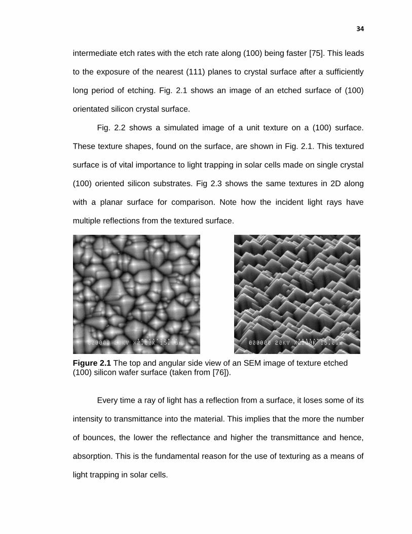
intermediate etch rates with the etch rate along (100) being faster [75]. This leads
to the exposure of the nearest (111) planes to crystal surface after a sufficiently
long period of etching. Fig. 2.1 shows an image of an etched surface of (100)
orientated silicon crystal surface.
Fig. 2.2 shows a simulated image of a unit texture on a (100) surface.
These texture shapes, found on the surface, are shown in Fig. 2.1. This textured
surface is of vital importance to light trapping in solar cells made on single crystal
(100) oriented silicon substrates. Fig 2.3 shows the same textures in 2D along
with a planar surface for comparison. Note how the incident light rays have
multiple reflections from the textured surface.
Figure 2.1 The top and angular side view of an SEM image of texture etched (100) silicon wafer surface (taken from [76]).
Every time a ray of light has a reflection from a surface, it loses some of its
intensity to transmittance into the material. This implies that the more the number
of bounces, the lower the reflectance and higher the transmittance and hence,
absorption. This is the fundamental reason for the use of texturing as a means of
light trapping in solar cells.

35
Figure 2.2 A simulated unit texture on (100) oriented silicon surface (taken from [77]).
Figure 2.3 Reflection of light from a textured surface and a planar surface.
Fig. 2.4 shows the reflectance of total 200 micron thick silicon wafers for
two cases (a) both sides planar, (b) both sides textured with a texture height of 3
microns, simulated in the new version of PV Optics. Note the large difference in
reflectance in both the cases. Due to this very reason, potassium hydroxide
etching has become an inseparable part of the production process of solar cells
based on single crystal (100) silicon substrates. But, in the case of solar cells
made on multicrystalline silicon substrates, a new surface texturing process has
to be used due to the random orientation of the each grain.

36
Figure 2.4 Reflectance for planar and textured silicon. Y-axis is the reflectance; X-axis is the wavelength of light.
It is generally believed that the active etching species for this process is
the hydroxyl (OH-) group [73, 78], derived from water in the etching solution. This
group reacts with the hydrogen terminated silicon surface molecules [79-81] to
form ionized hydroxyl terminated silicon complexes in water [73]. This step is
achieved by the breaking of the back bonds of the surface silicon atom, which it
forms with other silicon atoms in the crystal lattice. Thereupon, a silicate is
formed which can then leave the crystal lattice into the etching solution and
release hydrogen gas in the process [78, 82, 83].
Alcoholic moderators like isopropyl alcohol (IPA) have also been
incorporated in the etching solution [84]. IPA causes a reversal in etch rates
along the (100) directions and the (110) directions compared to the case when
no IPA is added to the etch solution [85]. It has also been observed that the
addition of IPA results in a higher density of textures on the silicon surface
compared to without the addition of IPA [86]. The main problem while adding IPA
to the etch solution is its low boiling point of 80°C. This is the temperature around

37
which texture etching is performed and hence, leads to the evaporation of IPA
with time leading to a variable etch solution. The way to circumvent this problem
is to conduct the etching process in a closed vessel with a condenser plate at the
top.
Following is the electrochemical reaction for the etching process with the
hydroxyl group as the reacting species [73]:
Si + 4OH- → Si(OH)4 (2.1)
Si(OH)4 + 2OH- → SiO2(OH)2-- + 2H20 (2.2)
4H20 + 4e- → 4OH- + 2H2 (2.3)
Even though the above reactions spell out the surface chemistry of the
etching process, there is no mention of the reasons for the anisotropic nature of
the reaction itself. This can only be found out by considering the silicon crystal
lattice itself. A detailed discussion on this can be found in ref [87] and the
references therein. Fig 2.5 shows a ball and stick model for a diamond crystal
unit cell.
It should be noted that the arrangement of the atoms in the silicon crystal
lattice is of ultimate importance when it comes to defining the anisotropic nature
of the etching process. The density of atoms on the surface, the number of
nearest neighbor surface bonds, number of nearest neighbor bulk back bonds

38
and the number of secondary neighbor atoms has an impact on the etch rates
[87].
Figure 2.5 Unit cell for a diamond crystal lattice, e.g. Silicon (taken from [88]).
2.1.2 Acid Etching of Silicon
Multicrystalline solar cells, with lesser efficiencies than single crystal solar cells,
have become the most important base material for solar cell production [89].
These cells need a texturing etchant that is not anisotropic. Since the crystal
orientations of various grains in a multicrystalline silicon wafer are random,
anisotropic etchants do not produce satisfactory light trapping properties [90].
Texturing with isotropic etchants have been found to produce much better light
trapping properties for these solar cells [91].
Acidic etchants which are based on HF:HNO3 systems are isotropic in
nature. The etching reaction is an oxidation-reduction reaction in which the
silicon is oxidized by HNO3 (nitric acid), and HF serves to remove the oxide. The
rate limiting factors are different for the HF rich regions and the HNO3 rich
regions. The oxidation of silicon by HNO3 limits the etch rate in the HF rich

39
regions while the removal of oxygen by HF is the rate limiting step in the HNO3
rich regions [86].
The texture shapes produced by acid etching include rough surfaces,
concave tub shaped pits, and smooth surfaces. The rough surfaces, produced,
have been of great utility and interest for the solar cell community as it can be
used as a means for reflection reduction from the cell surfaces [91-93]. Since this
etch is not orientation dependent, it results in the uniform texturization of the
complete surface of a multicrystalline silicon wafer compared to only the near
(100) oriented grains, as in the case of KOH etching.
The acid etching solution is made by diluting the HF:HNO3 system either
in water or acetic acid (CH3COOH). Since this reaction is an oxidation-reduction
reaction, i.e., it depends on electron transfer processes, the etch rate varies for n
and p-type materials, and for different doping densities [69, 94-96]. HNO2 is the
active oxidizing species with the reaction being:
4 HNO2 + Si → SiO2 + 2 H2O + 4 NO (2.4)
HNO2 in the above reaction forms by an autocatalytic, two-step process,
i.e., HNO3 reduces to form HNO2. This is the slow rate-determining step. The
second reaction generates more HNO2 by:
HNO2 + HNO3 ↔ N2O4 + H2O (2.5)

40
N2O4 + 2 NO + 2H2O ↔ 4 HNO2 (2.6)
The overall chemical reaction can be summarized as:
4 HNO3 + 2 Si → 2 SiO2 + 4 HNO2 (2.7)
Figure 2.6 SEM image of the surface of an acid etched silicon wafer (taken from [97]).
Crystal imperfections and defects can also initiate the etching process. A
detailed discussion on the surface morphology of acid etched wafers can also be
found in [86]. Fig. 2.6 shows an SEM image of the surface of an acid etched
silicon wafer [97].
2.1.3 Mechanical Texturing
Mechanical texturing of silicon wafers has been tried for light trapping purposes
[98-102]. In this process, as the name suggests, the surface of a silicon wafer is
grooved into V-shaped structures using a dicing saw with beveled blades. The

41
texturing can produce V grooves of various angles depending on the placement
and angle of the blades. Fig 2.7 shows a standard structure of a mechanically
grooved solar cell substrate [100].
This process was envisaged as an alternative to KOH and NaOH texture
etching as potassium and sodium are detrimental to the performance of a
semiconductor device and need subsequent cleaning steps. But with this
advantage, this process has its own set of limitations as well. These
disadvantages include low processing speed, tool wear, kerf loss and the sawing
damage issues [99].
Figure 2.7 Standard solar cell made from mechanically grooved multicrystalline silicon (taken from [100]).
The mechanical grooving process, in many cases, is also followed by a
one-step etching treatment of the substrate with HF:HNO3:CH3COOH [102]
solution to remove mechanically-damaged regions and to form porous silicon
layers; or a step of isotropic etching for damage removal [99]. Fig. 2.8 shows a
highly magnified SEM image of (a) 35° and (b) 60° mechanically grooved V
structures on a silicon substrate [99].

42
(a) (b)
Figure 2.8 Mechanically grooved structures at (a) 35° and (b) 60° (taken from [99]).
2.1.4 Reactive Ion Etching
Reactive ion etching (RIE), like acid etching, is also an isotropic etching process
that produces uniform surface texture irrespective of the crystal orientation of the
silicon substrate (e.g., [103]). In this process, a gas glow discharge is used to
dissociate and ionize relatively stable molecules to form highly reactive chemical
and ionic species [104]. Hence, unlike the acid or KOH etching, this is a dry
etching process. These reactive species are then directed to the substrate
surface where the etching takes place forming volatile products in the process.
The etch gas consists of a chemical etchant for etching the substrate, a
passivator for blocking the etching of sidewalls and an ion source for local
removal of passivator at the bottom of the etch trenches [105]. In the case of
silicon, a mixture of SF6, O2, and CHF3 is widely used [106]. SF6 provides F-
radicals for etching the silicon that leads to the formation of volatile SiF6 as a
reaction product. O2 gives O* radicals which passivate the silicon substrate with

43
SiOXFY, while CHF3 gives CFX+ ions which remove the passivating SiOXFY to give
COXFY. Fig 2.9 shows the setup for RIE.
Figure 2.9 Setup for Reactive Ion Etching (taken from [107]).
Following are the steps that take place during RIE [108]:
The gas mixture stated above is passed through a plasma chamber where a glow discharge, by electron-impact dissociation/ionization, creates the etching environment consisting of neutrals, electrons, photons, radicals (e.g. F*) and positive (e.g. SF5
+) and negative (e.g. F-) ions. Low energy ions (20-90eV) are used for a high etch selectivity and for low damage to the substrate and passivating layers.
As shown in Fig. 2.9, silicon wafers are placed on an r.f. driven capacitatively coupled electrode. After ignition of the plasma, the electrode acquires a negative charge, i.e., the d.c. self-bias voltage, because the mobility of electrons is much greater than the mobility of ions.
Due to diffusion, the reactive intermediates are transported from the bulk of the plasma to the silicon wafer surface. The positive ions too are forced to the surface from the glow region by the d.c. self-bias. These assist in the etching process as well.
The reactive radicals adsorb on the silicon surface.
Reaction between the adsorbed species and silicon takes place. SiF6, a volatile compound, is produced as a byproduct of this reaction.

44
The volatile byproduct is desorbed from the silicon surface into the gas phase.
The desorbed species diffuse from the etching surface into the bulk of the plasma and are pumped out of the system.
Figure 2.10 SEM pictures of surface structures on silicon wafers after RIE using (a) SF6/O2~ 1:0.7, (b) SF6/O2~ 1:1, (c) SF6/O2/Cl2 mixture and (d) SF6/O2/Cl2 mixture top view (taken from [109]).
This process leads to the formation of needle-like structures. The
diameters of these structures and the separation between them are small
compared to the useful solar wavelengths. Their heights are also comparable
with or larger than these wavelengths [110]. This provides the adequate surface
roughness to function effectively to trap light. Fig 2.10 shows an SEM image of
these structures [109].
45
Even though this process is very potent in reducing the reflectivity of a
silicon substrate and, thereby, increasing the absorbance, it increases the
surface area by orders of magnitude. This creates a big challenge to passivate
such a large surface area. Surface recombination of carriers can be a major
problem in this case.
2.1.5 Laser Texturing
The method of using lasers to texture the surface of a silicon wafer was first
published by Zolper et al [111]. This technique exploits the ablative properties of
textures to remove small amounts of materials from the silicon wafer surface to
produce grooves [111] or pits [112]. The pulse widths of these lasers are
extremely small: generally in the range of tens of nanoseconds although
femtosecond lasers have also been used for such texturing [113-117].
Laser texturing is a two-step process [112]. In the first step, the silicon
surface is first sculpted by laser ablation. This gets rid of the bulk of the silicon
required for texturing. The depth of the grooves or pits can be controlled by the
power of the laser. In the second step, the surface is chemically etched to
remove the slag. This leads to the smoothening of the surface and etching away
of any residual layer of laser damage.
The etching process must remove all of the ablation slag from the textured
surface and remove laser-damaged silicon to prevent the propagation of
dislocations into the bulk of the wafer [118]. This etching is done first by an
anisotropic etch (NaOH solution) followed by isotropic etching [113], although UV
lasers have been used recently where this etching step is not required [119]. Fig.

46
2.11 shows the surface of a silicon wafer after laser texturing. Note the uniform
spikes formed on the surface.
Figure 2.11 SEM image of the surface of a laser textured silicon wafer ( taken from [120]).
2.2 Other Light Trapping Techniques Light trapping techniques, discussed in the previous section, are based on
roughening the surface of the silicon substrate to maximize absorption.
Randomly roughened surfaces can theoretically enhance the path length of light
by fifty [121] times while the best realized result around ten times [122]. These
enhancements are sufficient for thick wafer based silicon solar cells. But due to
the indirect band gap of silicon and hence, the low absorbance, this
enhancement is entirely inefficient for thin film silicon solar cells.

47
Many light trapping techniques other than texturing have been developed
for thin film silicon solar cells. This section will give a brief overview and review of
these technologies relevant for silicon photovoltaics.
2.2.1 Diffraction Gratings
A repetitive array of diffracting elements, either apertures of obstacles, that has
the effect of producing periodic alterations in the phase, amplitude, or both of an
emergent wave is said to be a diffraction grating [123]. The grating equation
states that:
, (2.8)
where, m is the diffraction order in integers, λ is the incident wavelength, n is the
refractive index of the material, p is the period of the grating, α and θ are the
incidence and the diffraction angles, respectively.
In the case of rectangular gratings, for grating etch depth t=λ/4nSi, nSi
being the refractive index of silicon, the zeroth order reflection is strongly
suppressed while the 1-order diffractions are left intact, bent by 90°. Proper
designing of diffraction gratings at the back side of a solar cell can bend the first
order reflection exceeding the critical angle of total internal reflection of silicon
(16.6°). This leads to total internal reflection at the front surface of the cell,
thereby, enhancing the absorption in the active region.

48
Figure 2.12 A solar cell design with diffraction grating at the back. ‘p ‘is the period of the grating, ‘si’ is silicon while +1 and -1 are the respective order reflections from the back surface.
This technique has been employed by many research groups to enhance
the absorption in thin film silicon solar cells (e.g.,[124-126]). Fig. 2.12 shows a
standard structure with diffraction gratings at the back surface.
2.2.2 Photonic Crystals
A photonic crystal is a periodic arrangement of dielectric or metallic material with
a lattice constant comparable to the wavelength of an electromagnetic wave. A
detailed description on this can be found in [127]. This category of materials
came into limelight after the publications by Yablanovitch [128, 129] and John
[129]. Photonic crystals are regularly repeating areas of high and low dielectric
constants. Photons, behaving as waves, either propagate through this structure
or they do not, depending on their wavelength. Wavelengths of light that are
allowed to travel are known as modes, and groups of allowed modes form bands.
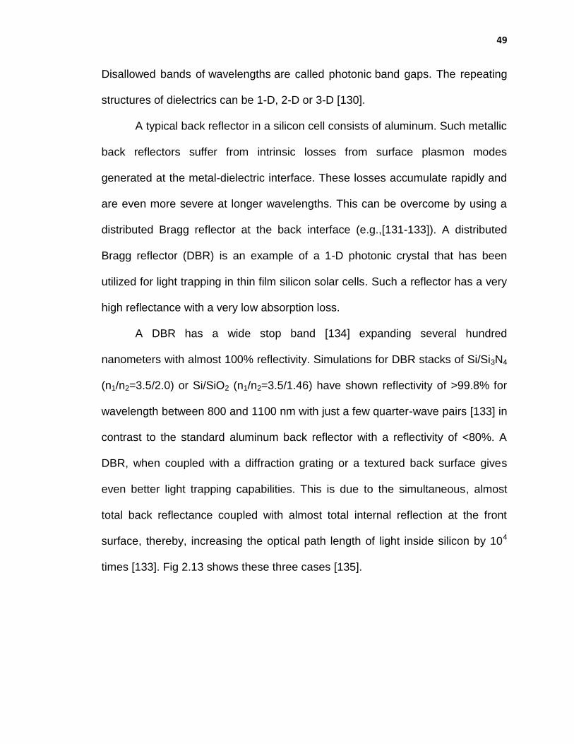
49
Disallowed bands of wavelengths are called photonic band gaps. The repeating
structures of dielectrics can be 1-D, 2-D or 3-D [130].
A typical back reflector in a silicon cell consists of aluminum. Such metallic
back reflectors suffer from intrinsic losses from surface plasmon modes
generated at the metal-dielectric interface. These losses accumulate rapidly and
are even more severe at longer wavelengths. This can be overcome by using a
distributed Bragg reflector at the back interface (e.g.,[131-133]). A distributed
Bragg reflector (DBR) is an example of a 1-D photonic crystal that has been
utilized for light trapping in thin film silicon solar cells. Such a reflector has a very
high reflectance with a very low absorption loss.
A DBR has a wide stop band [134] expanding several hundred
nanometers with almost 100% reflectivity. Simulations for DBR stacks of Si/Si3N4
(n1/n2=3.5/2.0) or Si/SiO2 (n1/n2=3.5/1.46) have shown reflectivity of >99.8% for
wavelength between 800 and 1100 nm with just a few quarter-wave pairs [133] in
contrast to the standard aluminum back reflector with a reflectivity of <80%. A
DBR, when coupled with a diffraction grating or a textured back surface gives
even better light trapping capabilities. This is due to the simultaneous, almost
total back reflectance coupled with almost total internal reflection at the front
surface, thereby, increasing the optical path length of light inside silicon by 104
times [133]. Fig 2.13 shows these three cases [135].

50
Figure 2.13 Illustration of three solar cell designs: (a) a simple design with a distributed Bragg reflector (DBR), which displays only spectral reflection, (b) a DBR plus a periodically etched grating, displaying spectral reflection and diffraction, and (c) a photonic crystal consisting of a triangular lattice of air holes, displaying simultaneous reflection, diffraction and refraction from the photonic crystal layer. Crystalline silicon is in the light green, low dielectric in light grey and air is transparent (taken from [135]).
2.2.3 Plasmonic Solar Cells
A novel method for increasing light absorption in thin film silicon solar cells that
has emerged comparatively recently is the use of scattering from noble metal
nanoparticles excited at their surface plasmon resonance. This is called the
Plasmonic Effect.
Interest in the plasmonic effect has intensified over the last few decades,
mainly due to the discovery that Raman scattering can be magnified many times
through the use of metal nanostructures [136, 137]. Stuart and Hall [138] did
pioneering work in the field of plasmonic enhancement of light-sensitive devices

51
when they showed that an enhancement in the photocurrent by a factor of 18
could be achieved for a 165 nm thick silicon-on-insulator photo-detector at a
wavelength of 800nm using silver nanoparticles on the device surface. Later,
Schaadt et al. [139] obtained enhancements of up to 80% at around 500nm
wavelength of light in highly doped wafer based silicon solar cells deposited with
gold nanoparticles. Derkacs et al. [140] also achieved an overall increase in
conversion efficiency of 8% in thin-film amorphous silicon solar cells by
depositing gold nanoparticles on the surface. Pillai et al. [141] reported a
sevenfold enhancement for wafer-based cells at λ=1200 nm and up to 16-fold
enhancement at λ=1050 nm for 1.25 µm thin silicon-on-insulator (SOI) cells when
deposited with Ag. Figure 2.14 shows a schematic of the plasmonic effect.
The photocurrent enhancement by metal particles incorporated into or on
solar cells has been explained by two main basic mechanisms:
Light scattering by metal nanoparticles, and
Near-field concentration of incident light.
Figure 2.14 A schematic of the plasmonic effect (taken from [141]).

52
Figure 2.15 SEM results and surface reflectance properties of the structure with different densities of Ag nanoparticles on the surface. (a) SEM image of sample with higher particle density. (b) SEM image of sample with smaller particles density. (c) Surface reflectance with different particle densities. (taken from [142])
Out of these two, scattering by metal particles has been the main
mechanism for enhancement of most reported experimental work. A detailed
description of the theory behind the scattering of light by plasmonic effect can be
found in ref. [143]. Figure 2.15 shows SEM images of silver nanoparticles on
silicon along with the optical reflectance curves.
2.3 Ray Tracing Simulations for Solar Cells: A Brief Review
For solar cells to become economically competitive with the conventional sources
of energy, optimizing their cost of production and efficiencies are of vital
importance. Proper optical and electrical design of solar cells and modules is one

53
of the major methods of achieving a harmony between cost and efficiency. While
there exist established commercial photovoltaic electrical modeling tools such as
PC1D [144] and AFORE-HET [145, 146], such optical modeling tools that can
handle complete solar cell structures do not exist. Some important photovoltaic
optical modeling tools available include: ray tracing softwares such as PV Optics
[50], BIRANDY [147], SUNRAYS [148], Texture [149], and APSYS [150, 151].
The first four software models can only handle 2-D structures using ray tracing
and lack options to include front metal architecture. APSYS, on the other hand,
integrates electrical and optical modeling for semiconductor devices including
solar cells, integrating Finite Element Analysis for electrical modeling with ray
tracing for optical modeling. Since this software is not photovoltaic specific, it is
not widely used by the PV community. This leaves a lot of room for introducing
front metal architecture into existing photovoltaic software packages.
Even though, as explained in the first chapter of this dissertation, ray
tracing has been used extensively for rendering computer graphics and lens
design, it has also found several applications in optical modeling of solar cells.
The first mention of ray tracing to study absorption of light in solar cells was
made by Redfield [152], which was followed by Yablanovitch [153] stating that an
enhancement of 4n2 (n is the refractive index) could be achieved by efficient light
trapping. The first study on light trapping of pyramidal textured silicon surfaces
was done by Campbell et al [55]. This was preceded by a ray tracing study on
light trapping of anisotropically etched III-V solar cells [154].

54
Texture, the ray tracing photovoltaic software mentioned in the beginning
of this section was released subsequently [149]. Wang et al subsequently used
ray tracing to study the light trapping capabilities of a PERL cell [155]. Smith et
al. later conducted a ray trace study of inverted pyramid texturing geometry and
reported its higher path length enhancement compared to pyramids and slats
[53].
SUNRAYS was released later which was used by Brendel to study the
light coupling into mechanically textured silicon solar cells [156]. Thorp et al. also
studied the light trapping in thin-film crystalline silicon solar cells deposited on
glass with a range of metal and detached reflectors at the back along with bifacial
modules which led them to conclude that a Jsc of 34-35 mA/cm2 could be
achieved under real conditions for a 10µm thick silicon film [147].
During this time, PV Optics was released as well [157]. This revolutionized
the field of software related to photovoltaics as it provided many more features
than any others in the market. Along with many new features, PV Optics added
the capability to model textured surfaces of varying angles with a two layer anti-
reflection (AR) coating [158]. This was followed by Nishimoto et al. conducting an
investigation into the light trapping characteristics of acid textured multicrystalline
silicon solar cells and found that the reflectance is directly dependent on the
quotient of the depth and the width of the texture [159].
Rodriguez et al. [160] were the first to propose a model for ray tracing
calculations on random pyramidal textured surfaces, using it to find that no metal
coating was necessary for a strong confinement of light within the silicon layer.

55
This model has been used extensively over the years. Figure 2.16 shows one
unit texture made using this model, where α is the fraction of the untextured area,
LT is the side of the enclosing cell and L is the base of the pyramid. Figure 2.17
shows a random pyramidal surface obtained using this model. This model was
recently used by Baker-Finch et al. to include polarization effects to optimize
refractive index of AR coatings for randomly textured silicon solar cells [161].
Figure 2.16 Unit cell. In regular textures, the ray reenters through a point that is symmetrical to the incident point. Reconstructed from [160].
Alkaline texture etching of (100) oriented silicon wafers is a standard
procedure for manufacturing single crystal silicon solar cells to reduce
reflectance and increase their efficiency. This kind of etching, being anisotropic in
nature, results in unique textures for each orientation. In the case of
multicrystalline silicon wafers, since the grains are randomly oriented, it leads to
texture shapes on the surface of each grain that directly correspond to its crystal
orientation leading to a unique reflectance value for each crystal orientation. This

56
provides an opportunity to ascertain the orientation of each grain by the shape of
the textures formed on its surface and its corresponding reflectance value.
Figure 2.17 Random pyramid surface using Rodriguez’s model. Reconstructed from [160].
2.4 Reflectance Calculations of Alkaline Textured Multicrystalline Silicon The random texturing model given by Rodriguez et al. [160] is extended to
handle textures for all crystal orientations. A rigorous 3D ray tracing computation
is carried out for multiple low index orientations to calculate their reflectance
leading to a model for calculation of the total reflectance of a complete 6”X6”
multicrystalline silicon wafer. Calculations have also been done for all crystal
orientations at a wavelength of 633 nm for a He-Ne laser source to make a one-
to-one orientation-to-reflectance map to aid in ascertaining the crystal orientation
of each grain by optical reflectance rather than by X-ray Laue patterns or EBSD
(Electron Back Scattering Diffraction). The calculated results have been verified

57
experimentally for each grain along with their crystal orientations. The
simulations and experimental results show an excellent agreement [86, 162].
2.4.1 Introduction Multicrystalline silicon has become the most important base material for silicon
solar cells in recent years [89]. This has led to a huge interest in ways to improve
the electronic properties of this material. Multicrystalline silicon consists of grains
of varying sizes and crystal orientations. It is known that grain boundaries act as
carrier recombination centers with the recombination activity dependent on the
grain boundary angles [163]. Hence, decreasing the grain boundary area and
angles in a multicrystalline silicon wafer is of vital importance in order to improve
performance of devices made on these substrates. This makes it imperative for
crystal growers to control and optimize the growth parameters of multicrystalline
silicon for better material quality and electrical performance. A thorough
knowledge of the correlation between crystal growth conditions and grain
orientations and grain boundary angles is also desirable. A fast and accurate
technique to determine these parameters for a multicrystalline silicon wafer
becomes even more important. As has been recently shown [59], the orientation
dependence of anisotropic etchants like potassium hydroxide solutions can be
exploited towards this end. The difference in reflectance of various grains can
also be utilized to increase the contrasts between grains in an optical image and,
thereby, used to calculate grain sizes and their distributions by employing image
processing techniques [59].

58
Even though wet chemical isotropic etching has been used in the silicon
semiconductor industry during processing since the 1950’s [68, 69], it took a little
while longer for anisotropic etching of silicon to follow suit [70, 71]. But it was only
during the mid-1970’s that this process was first introduced for silicon solar cell
processing [72]. It is known that the (111) direction has the slowest etch rates
[69] to alkaline etches compared to all other orientations. The comparative etch
rates of the basic orientations are R100>R110>R111, where Rhkl is the etch rate in a
specific crystallographic direction. This phenomenon results in the exposure of
the family of (111) planes nearest to the surface of the silicon substrate, when
etched anisotropically for a suitable duration of time.
In order to exploit the anisotropicity of alkaline etches towards silicon to
the fullest, a computer program, written in C++, has been developed to model the
textured surfaces of any arbitrarily oriented grain and perform rigorous ray tracing
simulations to calculate their reflectance. This model is based on the one given
by Rodriguez et al [160] for random textures on a (100) silicon surface after
anisotropic etching, which has been extended to handle textures on silicon
surface of any arbitrary crystal orientation after an alkaline etching process. This
model is presented here in detail, as there exist nothing in the literature that
handles this topic satisfactorily. Furthermore, the technique of ray tracing, being
a standard process for optical computations in solar cells [50], is not elaborated
in depth. The results of the calculations are also compared with the experimental
data available in the literature.

59
2.4.2 Modeling Textured Silicon Surface
The anisotropic etching of silicon using KOH exposes the family of (111) planes
nearest to the crystal surface. The vectors binding these planes are used to
define these (111) planes. Fig. 2.18 shows this family of planes in the orthogonal
coordinate system. The texture shape is completely dependent on the orientation
of the grains in a multicrystalline silicon wafer relative to these planes.
Fig. 2.18: The family of eight (111) planes with respect to the X, Y and Z-axes. The eight planes are ABE, ADE, CDE, BCE, ABF, ADF, CDF and BCF. The planes are symmetric about each of the six vertices, A, B, C, D, E and F.
The blue lines signify the edges of each plane. It should be noted that
these planes form two pyramids, one inverted while the other vertical. The set of
binding lines for each plane are used as reference to ascertain the texture shape
for any given crystal orientation. The points of intersection in Figure 2.18 are
marked from A-F. The lines are defined as follows for a texture of unit height of:
60
(2.9)
(2.10)
(2.11)
(2.12)
(2.13)
(2.14)
(2.15)
(2.16)
In order to define the surface textures, the crystallographic plane parallel
to the wafer surface is also defined mathematically. These planes are denoted in
terms of the angle that the normal to the surface of a plane from the origin makes
with the X-Y plane and the azimuth. Figure 2.19 shows these two angles used for
calculations.

61
Fig 2.19 The angles θ and φ for the unit normal to the crystallographic plane.
Thus, the surface of a grain of a known orientation can be expressed as a
3D plane passing through the origin and defined in terms of the angles and
using the equation:
(2.17)
Table 2.1 θ and φ for some low index crystallographic orientations.
Crystal Plane
(hkl)
θ φ
(100) 0° 0°
(310) 0° 18.435°
(210) 0° 26.565°
(311) 17.55° 18.435°
(211) 24.09° 26.565°
(321) 15.5° 33.69°
(110) 0° 45°
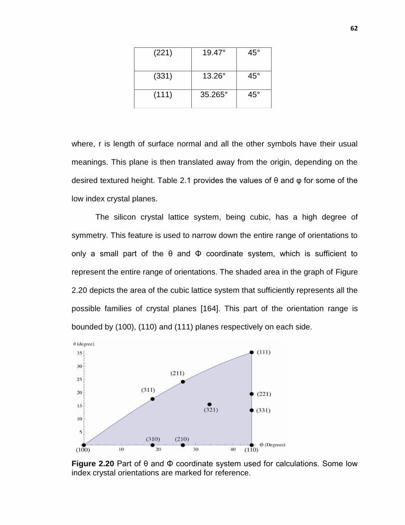
62
where, r is length of surface normal and all the other symbols have their usual
meanings. This plane is then translated away from the origin, depending on the
desired textured height. Table 2.1 provides the values of θ and φ for some of the
low index crystal planes.
The silicon crystal lattice system, being cubic, has a high degree of
symmetry. This feature is used to narrow down the entire range of orientations to
only a small part of the θ and Φ coordinate system, which is sufficient to
represent the entire range of orientations. The shaded area in the graph of Figure
2.20 depicts the area of the cubic lattice system that sufficiently represents all the
possible families of crystal planes [164]. This part of the orientation range is
bounded by (100), (110) and (111) planes respectively on each side.
Figure 2.20 Part of θ and Φ coordinate system used for calculations. Some low index crystal orientations are marked for reference.
(221) 19.47° 45°
(331) 13.26° 45°
(111) 35.265° 45°

63
The determination of the textured surface is based on what is defined as a
Unit Texture. A unit texture is one that is formed by the intersection of the nearest
(111) planes with the silicon crystal surface orientation plane. Such multiple unit
textures, when juxtaposed side-by-side, form a periodic anisotropically etched
silicon surface. The unit texture shape is calculated by the points of intersection
of the vectors forming the (111) planes with the equation of the crystallographic
planes, as given in Eq. 2.17. Figures 2.21(a) and (b) depict this process of unit
texture formation for (210) crystallographic plane.
(a) (b)
Figure 2.21 (a) Intersection of the family of (111) planes with the (210) crystal plane, (b) top view of unit texture thus formed.
The (210) plane calculated using Eq. 2.17 passes through the origin.
Hence, it is translated along the unit normal from the origin to the plane, so that it
intersects the (111) planes only on one side of the X-Y plane. This is shown in
Figure 2.21(a) where the surface (210) crystallographic plane is offset from the
origin by a unit length normal to it from the origin. Figure 2.21(b) shows the top
view of the part of the (111) planes above the (210) plane. The base of the unit
64
texture so calculated does not coincide with the X-Y plane. For ray tracing
computations, the complete silicon wafer structure is made parallel to the X-Y
plane. In order to make it lie on the horizontal, 3D rotation matrices [165] are
used to rotate the unit texture by θ and φ along the respective axes. Adjusting
the intersection points of the unit texture to get the desired texture height follows
this step. Once the unit texture is calculated, such multiple structures are placed
side by side to form a 4X4 array of surface texture. Figure 2.22 shows the
calculated textured surfaces for three low index orientations. These are
compared with the data from the literature in the same Figure. The calculated
unit textures are the same as those produced upon etching, even though texture
coverage area on the silicon surface is dependent on the etching solution and
conditions. Using proper etch masks along with etch conditions would lead to
surface textures resembling very closely to the calculated periodic textures.
Figure 2.23 shows the calculated periodic surface textures for a few other low
index crystallographic orientations.

65
Figure 2.22 SEM images of textured surfaces on the left (taken from [86]) and calculated periodic surface textures on the right for: a. (100), b. (311) and c. (321) crystal orientations.

66
2.4.3 Ray Tracing algorithm
Ray tracing computations have been done for hemispherical reflectance and
transmittance. The structure for reflectance computations consists of the wafer
structure constituted by (a) textured front surface, (b) textured back surface, (c)
the entire thickness of of the silicon wafer, and the detectors where rays are
captured when they leave the wafer, consisting of (d) detector plane on the top
to capture reflected rays and (e) detector plane at the bottom to capture the
transmitted rays. The wavelength range for computation is from 0.4 µm-1.1 µm.
Rays are incident on the middle portion of the texture array for these calculations.
Figure 2.23 Calculated periodic textures for anisotropically etched a. (211), b. (210) and c. (310) silicon.
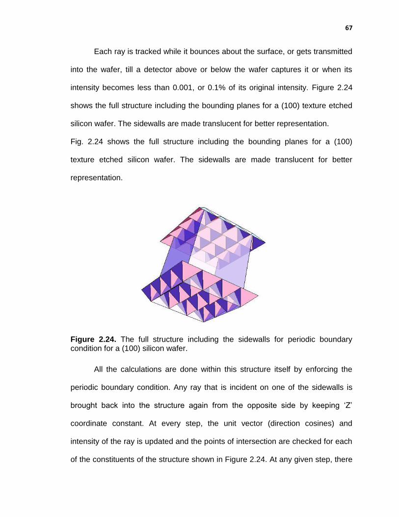
67
Each ray is tracked while it bounces about the surface, or gets transmitted
into the wafer, till a detector above or below the wafer captures it or when its
intensity becomes less than 0.001, or 0.1% of its original intensity. Figure 2.24
shows the full structure including the bounding planes for a (100) texture etched
silicon wafer. The sidewalls are made translucent for better representation.
Fig. 2.24 shows the full structure including the bounding planes for a (100)
texture etched silicon wafer. The sidewalls are made translucent for better
representation.
Figure 2.24. The full structure including the sidewalls for periodic boundary condition for a (100) silicon wafer.
All the calculations are done within this structure itself by enforcing the
periodic boundary condition. Any ray that is incident on one of the sidewalls is
brought back into the structure again from the opposite side by keeping ‘Z’
coordinate constant. At every step, the unit vector (direction cosines) and
intensity of the ray is updated and the points of intersection are checked for each
of the constituents of the structure shown in Figure 2.24. At any given step, there

68
will be multiple intersection points with many constituents of the wafer structure.
Each point of intersection is checked for validity, i.e., whether it lies within the
structure and not outside it, and whether it lies in a region shaded by another
structure, till the correct intersection point is identified. The reflection coefficient is
also calculated at every valid intersection point. If the ray hits one of the
bounding side planes, the reflection coefficient is taken to be 0 while the
transmission coefficient is taken to be 1. When the ray gets inside silicon, its
intensity is reduced depending on the absorption coefficient of silicon for the
wavelength of incident light under calculation.
The reflection and transmission coefficients formulae have already been
discussed in Chapter 1 of this dissertation. The intensity of the ray is diminished
upon absorbance by:
(2.18)
where,
is the absorption coefficient and is the extinction
coefficient. Finally, the reflectance for the entire surface is given by:
∑
(2.19)
where, Rfi is the final reflection coefficient of the ith ray, Rtot is the total
reflectance of the textured surface and n is total number of incident rays. This
entire sequence of calculations is carried out till all the incident rays have either

69
been absorbed by the substrate or captured by one of the two detectors. The
flowchart of the ray trace algorithm, implemented in C++, is shown at the end.
2.4.4 Results and discussion
Two types of calculations have been presented for different purposes:
(1) Complete reflectance curves are shown for seven low index crystallographic orientations due to constraint of space. These are: (100), (110), (111), (210), (310), (311), and (211). These reflectance values are compared with a polished silicon wafer.
(2) Calculations have also been done for silicon in the entire range of crystallographic orientations for a wavelength of 633 nm He-Ne laser source.
Figure 2.25(A) shows the calculated reflectance curves for periodically
textured wafers with thickness of 180 μm and texture height of 3 μm while Figure
2.25(B) shows the measured reflectance curves taken from the literature for
initial silicon thickness of 525 μm [86]. The trends in the reflectance curves are
very similar. The quality of texturing and the texture coverage on the surface of
silicon have a very important effect on the reflectance from silicon surface. The
variations in the reflectance between the calculated and measured values are
attributed to this. A more uniform texturing process than the one used in
reference [86] would result in very close match with the calculated values.
Figure 2.26 shows the 3D reflectance curve at a wavelength of 633 nm for
crystal orientations spread out in the region shown in Figure 2.20. Silicon, with an
orientation of (111), has the highest reflectance while the one at (100) has the
lowest reflectance with (110) having a reflectance value in between these two.
This is a unique curve where no two points have the same reflectance. The curve
increases monotonically from (100) to (111) and also from (110) to (111). This

70
provides a validation to the technique of using the hemispherical reflectance of
textured multicrystalline grains to ascertain their orientation.
Figure 2.25 (A) Calculated reflectance curves for a few alkaline texture-etched low index crystallographic orientation and polished silicon, (B) Reflectance in air for the texture etched wafers (initial thickness ~525 µm) compared to polished 100 µm silicon. (a) (111), (221) & (110), (b) (311) & (210) orientations [86].

71
2.4.5 Conclusions
A versatile algorithm to model the texture shapes on alkaline texture etched
silicon of any arbitrary (hkl) orientation has been developed. This model has
been implemented in a computer program written in C++ to calculate the
reflectance of individual grains of a texture etched multicrystalline silicon wafer.
Calculated results for various silicon crystal orientations show that the reflectance
of alkaline texture etched individual grains can be used to ascertain their crystal
orientation with a high degree of accuracy. This, however, would be dependent
on the quality of surface texture produced after the etching process.
Figure 2.26 The reflectance graphs for numerous alkaline texture etched silicon crystal orientations.

72
2.5 Summary In this chapter, a brief overview of various light trapping schemes have been
provided. This has been supplemented with an overview of the developments in
the field of ray tracing computations for solar cells. The work done by the author
of this dissertation to calculate the reflectance of alkaline texture etched
multicrystalline silicon wafers and its subsequent use to develop a new and ultra-
fast grain orientation mapping technique has also been presented in detail. It is
very clear from the literature that optical modeling, using ray tracing, is a powerful
tool for the design of solar cells and modules and this chapter will serve as a
prelude to the detailed explanation of the new optical model developed for
simulations in finished solar cells.

73
Figure 2.27 Flowchart for ray tracing computation
74
CHAPTER 3
DETAILED OPTICAL MODEL AND PROGRAM ALGORITHM
3.1 Introduction
There exist a quite a few ray-tracing programs and models that are capable of
handling complex surfaces and multiple device layers. Some of them, like PV
Optics, are excellent in giving meaningful and valuable information about light
trapping features for real world solar cell and module designs. However, they do
not have any provisions to add front metal architectures into the cell structure.
This serves as a major limitation for solar cell and module designers to optimize
front metal electrode structures and geometries. The main reason for this
shortcoming is the fact that no model has been developed yet to simulate the
interaction of light with a complete solar cell device structure including the front
metal electrodes.
Introduction of front metal electrodes to the standard device structures
renders the simple periodic boundary conditions used in models implemented in
various solar cell optical simulation software packages to be useless. Even the
most complicated of models like the ones that generate random textures on the
surface of a (100) textured silicon wafer in 3-dimensions (3D) deal with only the
air and silicon interface at the front end. With the introduction of front metal
electrodes, a new metal layer is superimposed on the front textured surface
leading to spatial non-uniformities and discontinuities in the cell structure. This
requires a new strategy to model the interaction between light and the complete
device structure. But before beginning to examine the complete

75
model, it would be pertinent to briefly explain the reason to use ray tracing over
other available numerical techniques.
Choosing the correct and appropriate numerical technique to solve a
complex problem like this can be a real challenge in itself. Finite Difference Time
Domain (FDTD) is one of the most widely used numerical techniques for optical
wave propagation simulations in solar cells and other structures [166-170]. It has
a very high rate of accuracy coupled with the ability to handle complex optical
wave phenomena. But its main drawback is the very high computing budget
required for calculations, which grows roughly as the fourth power of the grid
resolution [171]. This makes it challenging for solving large area problems with a
limited computing capacity, such as using a desktop or a laptop.
While developing the optical model for solar cells, explained in this
dissertation, there were a few clear-cut goals and targets that had to be
achieved. Two of the main objectives were: (a) that the model so developed
should be highly accurate and stand up to experimental scrutiny, and (b) the
software should require the minimum computing budget possible. Creating a
harmony between these two seemingly disparate goals was really challenging
indeed. The main reasons and motivation behind choosing ray tracing as the
preferred path were the following:
Since the dimensions involved in commercial wafer based silicon solar cells, like thickness, texture heights, front metal contact dimensions etc., are much larger than the wavelength of useful incident light from the sun, which renders ray tracing completely valid.
Ray tracing has a unique property whereby aspects of explicit wave nature of light, like behavior in anti-reflection coatings etc., can be

76
readily included without increasing the required computing budget and making this process highly accurate as well [158].
The computing budget required for this kind of an algorithm or program is smaller compared to other computing methods, as the mesh sizes are lot larger for ray tracing simulations. For example, for good accuracy, the mesh size for FDTD calculations has to be lesser than one-tenth the wavelength of the propagation optical wave (λ/10), also called the Courant Factor [166].
No need for fast, fancy and expensive computers, thereby enlarging the user base.
This chapter will explain, in detail, the model developed to implement the
introduction of front metal architecture in alkaline texture etched (100) single
crystal silicon solar cells and the program algorithm implemented in C++. This
will include strategies to use the inherent symmetry in surface texture and cell
design to reduce the computing area of the cell as well as the computing time
while maintaining high calculation accuracy.
3.2 Model for Optical Calculations in a Finished Solar Cell
At present, solar cell technology has matured to an extent where each
commercial solar cell is typically made on 6 in. X 6 in. semiconductor substrates.
Performing computation on such a large area in a full scale 3D model is both
time consuming and redundant. A simpler 2D model has been developed which
reduces the computational time by at least an order of magnitude without any
loss in accuracy. Furthermore, the software developed has the capability to
implement various structural parameters of the device for cell and module study
and design.

77
The starting point for the development of this model is to come up with a
way to reduce the 3D device structure to a 2D. This is of paramount importance
for two reasons: (a) there is practically no loss in computational accuracy due to
this transformation, and (b) the computation time and budget are reduced by at
least one order of magnitude.
Once the complex 3D structure is transformed to a corresponding 2D
structure, the incident photon flux needs to be defined in terms of ray optics. As
discussed in Chapter 1 of this dissertation, the AM 1.5 spectrum is used as the
standard for solar cell testing as well as modeling. We do the same in our
calculations. The formulation for the photon flux in terms of ray optics has to deal
with two issues: (a) the correlation between the intensity of a ray of light to the
total area illuminated, and (b) the effect of the angle of incidence on the photon
flux density reaching the surface of the solar cell. As will be explained in detail,
later, ray optics reduces an optical wave propagation problem to a problem of
sampling the surface and volume. This implies that the higher the density of rays
incident on the device surface, the higher is the accuracy of the calculations.
The next step in the modeling process is to (a) identify the inherent
symmetries in the device structure, and (b) understand the inherent differences
arising out of the introduction of front metal contacts. These are important to
reduce the computation time and, more importantly, to devise the final integration
step for complete device volume over the full range of incident wavelengths of
light. This integration step is of vital importance as it provides the final results for
the calculations.
78
In order to exploit the symmetry due to texture and device structure in
alkaline etched single crystalline solar cells, the complete device area is divided
into three regions for computational purpose, depending on their proximity to the
front fingers and bus bars. This calls for three separate computations, one for
each of these regions. Finally, once all the above-mentioned processes and
computations have been realized, the results are integrated for complete device
volume over the full range of incident wavelengths of light, giving the results for
the entire computation.
3.2.1 3D Structure Transformation to 2D
(100) oriented single crystalline substrates are textured by etching with alkaline
etchants to reduce reflectance from their surface. The resulting surface is filled
with four-sided pyramids with square bases. These pyramids are generally
randomly ordered with each of their four faces at an angle of 54.74° to the
horizontal. A regular array of these pyramids can also be formed with the use of
proper masking on substrate surface.
For the purpose of the new model, a regular array of pyramids is assumed
on the back as well as the front surface of a silicon wafer. It has been found to be
a very good approximation to a randomly textured surface. Figure 3.1 (a) shows
a 2X2 array of such pyramids from the top while Figure 3.2 (b) shows the array
from the one side.
As can be seen in the Figure 3.1, one pair of opposite faces of the 3D
texture in Figure 3.1(a) can be approximated with the 2D structure shown in
Figure 3.1(b), with a few modifications. Figure 3.2 shows the 3D view of the front

79
and the back side of an alkaline etched (100) silicon substrate. The complete
device structure for a standard commercial single crystalline solar cell also
consists of a back metal electrode. Figure 3.3 shows the side view of such a
device in 2D. The correlation between the 3D structure and the 2D structure in
Figures 3.2 and 3.3 is self-evident.
(a) (b)
Figure 3.1 (a) Top view of an array of 2X2 pyramids, (b) side view of the textures.
Figure 3.2 A 3D image of the front and backsides of an alkaline texture etched (100) silicon substrate.

80
As shown in Figure 3.3, the complete 2D structure is made up of Unit
Cells. A unit cell is a single mesh created for the calculations. In other words,
each of the square pyramids shown in Figure 3.1(a) makes up a unit cell, which
encompasses the full thickness of the device, as shown in Figure 3.4. The
dashed blue line in Figure 3.3 shows such a unit cell.
Figure 3.3 The standard structure 2D used for calculations without front metal.
(a) (b)
Figure 3.4 (a) The standard structure used for calculations (marked in blue dashed lines in Figure 3.3), and (b) deduction of this structure from 3D.

81
Note that the Figure 3.4 is a magnified view of one of the V-shaped
textures shown with dashed blue lines in Figure 3.3. This unit cell is the basis of
the calculations performed for the complete finished solar cell. This is the same
structure used in calculations for PV Optics.
The black rays shown in Figure 3.4 show the incident and reflected rays
while the red and blue rays show the transmitted light in the device structure.
Note that the texture angle equals that of a (100) textured surface shown in
Figure 3.1(b).
Figure 3.4(b) shows exactly how two adjacent faces of the pyramidal
surface constitute the corresponding 2D surface. The dark blue and the red
arrows show incident light on each of these two faces. As can also be seen, this
structure does not include the front metal fingers or busbars.
The side boundaries in this structure enforce the periodic boundary
conditions for calculations. Whenever a ray of light hits any one of these
boundaries, it is translated along the ‘X’ axis and brought into the cell structure
from the boundary on the opposite side. The reflection coefficient at these
boundaries is taken to be 0 while the transmission coefficient is taken to be 1,
i.e., the intensity of the ray does not change upon striking any of the boundaries
and then are brought back from the opposite side.
Whenever a ray of light is incident on any of these boundaries, it is
translated along the ‘X’ axis and brought into the cell structure from the boundary
on the opposite side. The reflection coefficient at these boundaries is taken to be
0 while the transmission coefficient is taken to be 1, i.e., the intensity of the ray

82
does not change upon striking any of the boundaries and is then brought back
from the opposite side.
The structure shown consists of only the silicon absorber layer and the
aluminum back contact. The black rays on the front surface denote the incident
sunlight while the red and blue rays denote the light that is transmitted into the
silicon substrate. The red rays explain the effect of the side boundaries. As can
be seen from the figure, once the red ray hits the left side wall, it is brought back
into the solar cell structure from the opposite side while keeping the Y coordinate
the same.
Figure 3.5 The front electrode architecture of a standard solar cell.
In order to include front metal contacts into this structure, it is necessary to
observe the structure for a complete solar cell. Figure 3.5 shows the top view of a
complete silicon solar cell. The thin white lines of the blue surface are called
Fingers while the two thick white lines running perpendicular to the fingers are
called Bus bars. They are made of silver and serve the purpose of extracting the
charged carriers generated in the bulk of the alkaline textured semiconductor

83
substrate lying below and placing them in the external circuit. This bulk
semiconductor region is shown in the same Figure in blue color. Figure 3.6
shows the 2D cross sectional view of the complete cell structure for fingers while
Figure 3.7 shows the same view for busbars. All these structures are made using
vectors. That is, each and every line segment in these structures is made using
vectors. Figures 3.4, 3.6 and 3.7 show the three areas that a solar cell is divided
into for the purpose of computations.
Figure 3.6 The 2D cross-sectional construction of fingers on textured silicon substrate.
In Figure 3.8, the 3D pyramidal structure is actually made up of two 2D
structures shown in Figure 3.4. When light is incident on each of the unit
textures, it is divided equally amongst each of the four faces. With the regular
pyramidal structure assumed for this model, incident light travels either parallel or
perpendicular to X and the Y-axes upon reflection as well as transmission into
the device structure. This leads to the possibility of modeling each of the unit
textures in 3D by two perpendicular structures shown in Figure 3.4. The rays

84
marked in black and blue in Figure 3.8 show each of these two perpendicular
directions.
Figure 3.7 2D cross-sectional rendering of a busbar for the complete device structure.
Figure 3.8 The pyramidal texture on (100) silicon surface. Note the pair of blue and black lines denoting the plane of propagation of reflected and transmitted light.
It is also assumed that the edges of each front metal contact starts and
ends at the tip of a pyramid. The width and the number of fingers on the front
surface vary from solar cell manufacturer to manufacturer. But, as a common rule

85
of thumb, the thinner and the lesser the number of fingers there are on a solar
cell, the better its optical performance should be. This is because the area
covered by the front metal electrode that shades the silicon substrate cannot see
any sunlight directly. It only has to depend on the diffused transmitted light
seeping into this region from the uncovered region.
It also has to be borne in mind that the bus bars and the fingers are lined
up perpendicular to each other. This implies that the 2D textured surfaces shown
below and on the sides of the fingers and the bus bar are perpendicular to each
other as well.
3.2.2 Effect of Photon Flux Incident Angle
After the complete solar cell structure has been defined mathematically, the next
step is to define the incident photon flux in terms of rays. The AM 1.5 spectrum,
as explained in Chapter 1 of this dissertation, is taken to be the standard photon
flux for the calculations. This is given in terms of per cm2. The incoming photon
flux is taken to be constant along the plane perpendicular to its direction of
incidence. Hence, this has to be weighed according to the incident angles of the
incoming rays. Figure 3.9 shows the relationship between the incident angle of
the photon flux and the incident photon flux density along the X-axis.
In Figure 3.9, θ is the angle of incidence of the photons, and hence also
the incoming rays. The intensity of the photon flux reaching the X-axis is given by
the following dot product:

86
(3.1)
where, IPh is the incident photon flux, IAM 1.5 is the AM 1.5 photon flux and is the
unit vector along Y- axis.
Eq. (3.1) translates to
(3.2)
where, is the angle of incidence of the incoming rays.
Figure 3.9 The incident photon flux at an angle with respect to the vertical (Y-axis).
The incident plane is divided up into a number of incident rays at equal
distances from each other. Each ray has an intensity of 1.0. As the rays move
about the computation structure, their intensity is reduced with each reflection
and by absorption in the silicon layer. In the end, once the computation for a
87
region is completed, the results are averaged for the total number of incident
rays.
3.2.3 Symmetry in a Solar Cell Structure and Computation Regions As has been mentioned earlier, the computational area is divided up into three
regions, depending on the proximity of each unit cell, under computation, to
either the front metal fingers or busbars. This can be understood by examining
the differences between calculations on a solar cell with and without the front
electrodes. In the case of no front electrodes, the incident rays only interact with
either of the two interfaces:
Air and silicon, and
Silicon and aluminum.
This is shown in Figure 3.10. The blue arrows denote the incident radiation from
the sun while the red arrows denote the transmitted rays into the device
structure. Note that the incident and transmitted light interacts with only the two
kinds of interfaces as mentioned above.
In the case of a structure with front metal electrodes, this is not quite the
case. The incident, reflected and the transmitted light can, in addition to the two
interfaces stated above, interact with two other interfaces depending on the
position and the direction of propagation: (a) air and silver, and (b) silicon and
silver. Figure 3.11 shows the other possibilities.
The incident light is drawn in blue rays while the transmitted light rays are
drawn in red and green. As can be seen, the red rays interact with the silicon and
silver interface while the green rays behave same way as shown in Figure 3.10.

88
‘d’ is the distance from the edge of a metal contact to the region where the last
transmitted ray interacts with silver-silicon interface. This difference in the two
calculation scenarios gives rise to the extra two regions for a structure with metal
contacts. The region shown in Figure 3.11 is one of those two regions. The
structure is scanned with incoming light rays till it reaches the point at a distance
‘d’ shown in the figure. The rest of the region perpendicular to the busbars
behaves exactly the same way as the case without any front metal contacts.
Figure 3.10 2D structure of the cross-section of a finished solar cell with no front metal. The blue arrows denote the incident rays while the red arrows denote the transmitted rays.
Figure 3.11 The progression of light rays in the case of a structure with front metal electrodes.

89
The same methodology is used for the area perpendicular to the fingers.
Figure 3.12 shows this region in greater detail. It has been found through
calculations that, in conventional commercial silicon solar cells, in the region
perpendicular to the fingers, light always interacts with the silicon-silver interface.
Hence, the scanning region encompasses the whole of the region in between two
consecutive fingers.
Figure 3.12 The region perpendicular to the metal fingers. ‘dF’ is the region in between two metal fingers.
The distance between two fingers is taken to be dF. By taking symmetry
into account, the scanning or computational area in between fingers is taken to
be dF/2 on each side of a metal finger. This is the region marked in between the
blue dashed lines in Figure 3.12. One such region is called a Master Cell which
in turn is made up of many unit cells. The fingers at either end of the horizontal
face of a solar cell are taken to be dF/2 distance away from the edges. This
means that once one such region is computed upon, the results can then be
multiplied by the number of total fingers in the solar cell under computation. In
summary, the three computation regions that a solar cell is broken down into are:

90
Region 1- The region where there is no interaction of transmitted light with the silicon-silver interface (Figure 3.10)
Region 2- The region near the busbars (perpendicular to the busbars) where the transmitted light interacts with the silicon-silver interface (Figure 3.11).
Region 3- The region in between the fingers denoted by the blue dashed lines as shown in Figure 3.12.
3.2.4 Integration of Calculations over the Entire Solar Cell
Once the calculations over the three regions have been completed, the results
have to be integrated over the entire volume of the solar cell to get the final
output. As has been mentioned before, the entire solar cell is divided into a mesh
for computational purposes. This process is known as meshing in numerical
calculations. Figure 3.13 shows the meshing pattern for a finished solar cell. Note
the array of 4X4 pyramids shown in the mesh for reference. Each unit pyramid
shown in Figure 3.1(a) constitutes one unit mesh, with the depth being the entire
thickness of the device.
All the structures and regions shown till now lie in this mesh. The
integration of the calculated regions is done for each of this mesh at the end. The
light incident on each of these meshes is divided into two equal parts: one
travelling in the direction of the blue rays, while the other half travelling in the
direction of the red rays. Each of these directions is portrayed by any of the three
regions explained above, depending on the placement of the unit mesh.
The total current generated in the complete volume of the solar cells is given by:
(3.3)

91
where, ISC is the current generated over the entire solar cell, IRegion1 to IRegion3 are
the currents generated in each unit mesh from region 1-region 3 while NRegion1 to
NRegion3 are the number of unit meshes in each of the three regions, respectively.
The back metal losses and the front metal losses are also calculated in the same
way as Eq. (3.3).
Figure 3.13 The top view of the meshing of a solar cell with a few pyramids shown for reference.
3.3 Conclusions
This chapter explains the full model, procedure and algorithm followed for
calculations in a finished solar cell upon the inclusion of front metal electrodes.
The complete 3D structure of the solar cell device is reduced to three subsequent
2D structures for computation. The entire volume of the solar cell is divided into
three separate 2D regions for the purpose of computation. The computation for
each region is done in series with the computation time reduced by at least an

92
order of magnitude as compared to full 3D computations. The results from each
of these regions are then integrated over the entire volume of the given solar cell
and over the entire range of useful wavelengths of incident sunlight. Refractive
indices and extinction coefficients for silicon, aluminum and silver are taken from
the existing database of PV Optics. The main values of interest from these
calculations are follows:
the total maximum current that can be generated from an entire finished solar cell assuming that each absorbed photon results in the generation of one electron-hole pair in the silicon bulk;
the maximum current that can be generated in the shaded region of the solar cell due to the diffusion of light;
the back and front metal optical losses over the entire solar cell;
the absorption profile beneath the shaded region, i.e., below the fingers and the busbars.
93
CHAPTER 4
SUMMARY OF RESULTS: SOLAR CELL
4.1 Introduction
The standard structure of a commercial solar cell, as explained in Chapter 3 and
Chapter 4 of this dissertation, consists of the following:
a semiconductor absorber layer with textured front and back surfaces to reduce reflectance and hence increase absorbance,
a p-n junction formed in the semiconductor absorber layer to aid in separation of the optically generated carriers,
a back metal contact to extract the optically generated charge carriers in the bulk of the absorber semiconductor layer.
a thin layer of anti-reflection coating on the front surface of the semiconductor absorber layer to further increase light trapping,
a front metal electrode grid pattern to complete the electrical circuit for carrier extraction from the absorber semiconductor layer.
As explained in Chapter 3 of this dissertation, the new model
incorporating all of the above structure components in solar cells has been
implemented in a computer program written in C++. This version of the software,
PV Optics 4.0, will soon be released for common usage. The user using this
program will have the freedom and option to vary various material as well as
structural parameters of a solar cell. The structural parameters that can be varied
by the user include the following:
the thickness of the silicon absorber layer,
texture angle and texture height with the option of having planar of textured back and front surfaces of the silicon absorber layer,

94
two layer anti-reflection coating at the front surface,
thickness and material of the back metal contact,
front metal electrode architecture:
i. width and height of a metal finger,
ii. spacing between metal fingers,
iii. thickness and height of the busbars,
iv. location of the busbars on the front silicon absorber layer
surface.
thickness and optical parameters of the solar cell encapsulant,
thickness and optical parameters of the glass enclosure.
These options provide the new software with flexibility and capability in
terms of choosing the solar cell structure. Calculations have been performed on
many solar cell structures using the new software. The main aim of these
calculations is to provide a trend in the optical performance of single crystal
texture etched solar cells made on (100) oriented silicon substrates while varying
various structural parameters. Table 4.1 specifies the structural parameters that
have been maintained constant for this study. This chapter provides the
simulation results for a stand-alone un-encapsulated solar cell while the next
chapter will summarize the effects of encapsulation of such a solar cell in a
module. All the calculations have been done for normally incident light on the cell
surface. This is the standard practice to optimize solar cell performance under
the effect of normally incident light. The optical parameters have been taken from
the existing database in the previous versions of PV Optics.

95
Table 4.1 The various structural parameters of a solar cell that have been maintained constant for calculations
Structure Parameters
Inputs Used in Calculations
Anti-reflection coating Two layers: (a) Native Silicon dioxide
(b) Silicon Nitride
Texture Angle 70.52° -For (100) texture etched silicon
Absorber Layer Material Silicon
Back Metal Contact Material Aluminum
Back Metal Contact Thickness 2 µm
Front Metal Contact Height 20 µm
Front Metal Contact Material Silver
As can be seen from the above table, the front metal contact height and
the back metal contact thickness are not varied for these calculations. In the case
of back metal contact thickness, because it is known that metals are highly
absorbing in nature, the variation in thickness of aluminum used in commercial
solar cells does not make any difference as all the light that is transmitted into the
metal is absorbed completely very close to the surface. For the case of front
metal contact height, any normally incident light would be reflected away from the
solar cell surface upon reflection from the sidewalls of front metal fingers. Figure
4.1 elucidates this more clearly. The rays signify the direction of the travelling
light. The case of encapsulation of a solar cell in a module and the effect of front
metal electrode height has been investigated in the next chapter.

96
Figure 4.1 The interaction of normally incident light with front metal.
4.2 Simulation Results
The effects of variation in the following structural parameters are investigated:
silicon absorber layer thickness,
finger thickness and spacing, and
texture height. 4.2.1 Variation in Silicon Absorber Layer Thickness Silicon, being an indirect band-gap semiconductor, has a low absorption
coefficient. This effect is especially pronounced as the wavelength of light
approaches the band-edge of silicon. Texture etching of silicon, using anisotropic
alkaline etches, is an effective method to increase absorption over the entire
useful solar spectrum. Hence, this has become a standard processing technique
for single crystal (100) oriented silicon solar cells. Thus, it also makes sense that
the more the thickness of the silicon absorber layer, the higher the optical
absorption, leading to more current being generated from the photovoltaic
device.

97
For the calculations, the thickness of the absorber layer has been varied
from 40 µm to 180 µm in five steps- 40 µm, 80 µm, 120 µm, 150 µm and180 µm.
Table 4.2 summarizes the various parameters that are kept constant for these
calculations and their corresponding values. These are not mentioned in Table
4.1.
Table 4.2 Parameters kept constant to study the effect of thickness on the performance of a solar cell
Parameters Kept Constant
Parameter Values
Texture Height
2 µm
Finger Width
100 µm
Busbar Width
2 mm
Number of Fingers
70
Number of Busbars
2
Solar Cell Dimensions
156 mm X 156 mm
For normal incidence, light is only shown on the exposed region of the
solar cell. Table 4.3 summarizes the results of these calculations. The Maximum
Achievable Output Current (MAOC) has the unit of Amperes (A) while the other
losses are given in terms of milli-Amperes (mA). MAOC is calculated assuming
that every photon generates one electron-hole pair and both these carriers have
a probability of 1.0 to be extracted from the solar cell bulk through the front and
back metal electrodes. Figure 4.2 shows the graphical plot of the calculated
MAOC results with respect to the absorber layer thickness. Figure 4.3 plots the
reflectance loss and the back metal absorption loss while Figure 4.4 plots the

98
percentage current generated in the shaded region of the solar cell with respect
to the absorber layer thickness. The reflectance loss shown in Table 4.3 is
calculated in terms of the number of photons reflected back from the solar cell
surface assuming that each photon, if absorbed, would have contributed one
electron-hole pair to the MAOC.
Table 4.3 Summary of calculated results for different absorber layer thicknesses and metal finger width of 100 µm
Absorber Layer
Thickness (µm)
Maximum Achievable
Output Current (A)
Reflectance Loss (mA)
Back Metal Absorption Loss (mA)
Front Metal
Absorption Loss (mA)
% age current
generated in the
shaded region
40
8.46 932.56 674.09 1.02 0.175
80
8.73 771.11 571.56 1.15 0.24
120
8.83 769.94 474.84 1.21 0.30
150
8.94 689.26 445.61 1.14 0.325
180
9.04 614.77
421.69 1.11 0.34
Figures 4.2 and 4.3 provide insight into the effect of the absorber layer
thickness on the optics of a solar cell. The plot in Figure 4.2 and the Table 4.3
show that there is a constant increase in the MAOC as the thickness of the
silicon absorber layer increases. It is also important to note that the increase in
current from 40 µm to 180 µm, an increase of 350%, results in the increase in the
MAOC by only 6.855%. This indicates that, with better wafer handling and light
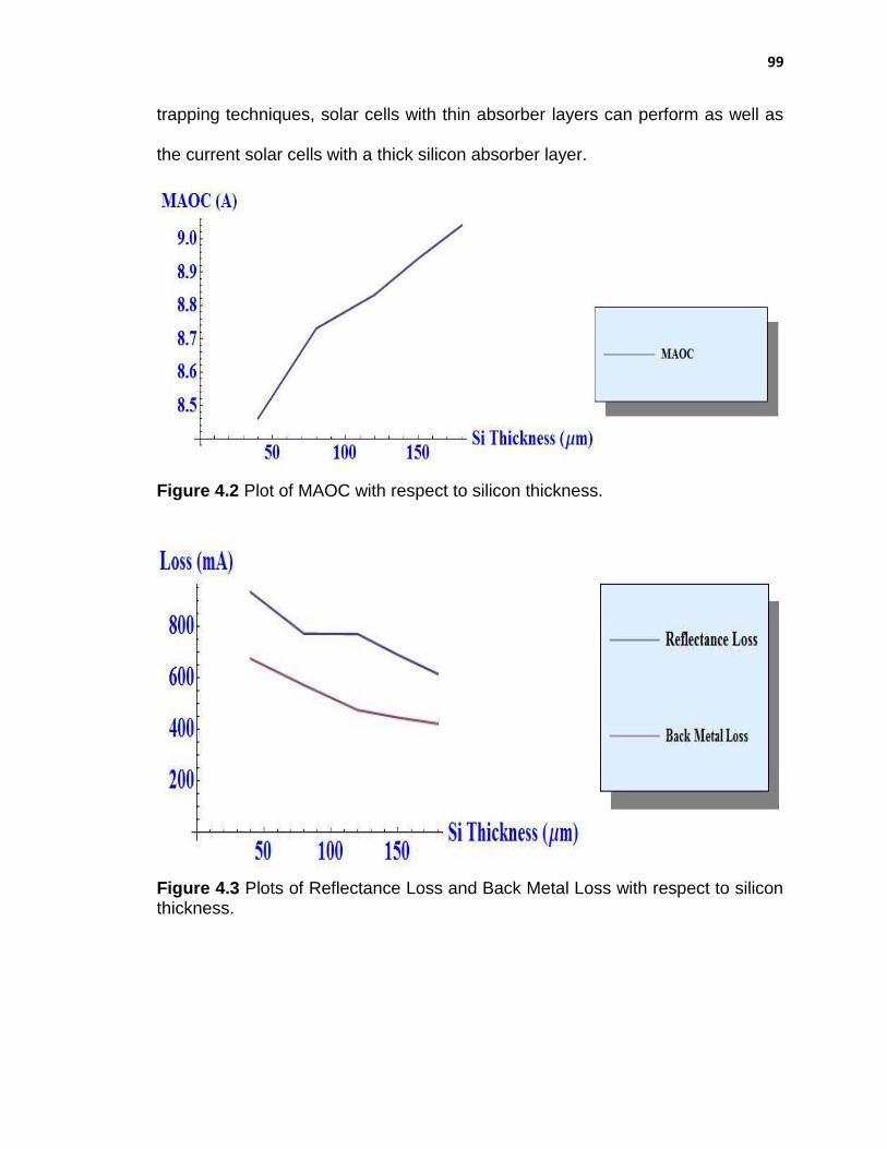
99
trapping techniques, solar cells with thin absorber layers can perform as well as
the current solar cells with a thick silicon absorber layer.
Figure 4.2 Plot of MAOC with respect to silicon thickness.
Figure 4.3 Plots of Reflectance Loss and Back Metal Loss with respect to silicon thickness.

100
Figure 4.4 Plot of percentage current generated in the shaded region.
Another important set of numbers to be taken into account while designing
a solar cell are the various losses accrued during its functioning. Some of the
various optical losses have been summarized in Table 4.3. These losses are:
Reflectance Loss: This is caused by the reflection of light from the solar cell and
air interface. The plot in Figure 4.3 shows the change in the amount of loss due
to reflectance with respect to the change in thickness of the silicon absorber
layer. Note that there is a constant decline in the reflectance loss from a solar cell
with an increase in the silicon thickness. This should imply that the reduction in
reflectance should yield a subsequent gain in the generated current. But on
closer examination, it becomes clear that the savings from the reflectance loss
add up to an increment in the current generated in the solar cell. This is due to
fact that, as the wavelength of light approaches the band edge of silicon, the
absorption coefficient decreases exponentially. Hence, the light that is

101
transmitted into the absorber layer at these wavelengths is not highly absorbed
which leads to the light travelling great lengths within the silicon substrate. Due to
the texturing of the silicon surfaces and the application of an anti-reflection
coating at the front end of the solar cell, the optical path-lengths within the silicon
absorber layer at these wavelengths is highly enhanced, leading to higher
absorption and hence an increase in the total current generated. As has been
stated earlier, better light trapping techniques would mean that this loss can be
reduced substantially for thinner silicon substrates than what is achieved
commercially at present. This light, upon travelling the entire thickness of the
silicon substrate, strikes the silicon-aluminum or the silicon-silver interfaces and
is absorbed by the metal at the contacts leading to what is called the Metal Loss.
Table 4.3 mentions two of these metal losses: back metal loss and the front
metal loss.
Back Metal Loss: This is the optical loss that occurs due to the parasitic
absorption of light by the metal at the back contact interface without actually
resulting in the generation of any electron-hole pairs. Figure 4.3 shows that the
amount of light lost due to this loss decreases as the thickness of the silicon layer
is increased. This is due to the increase in the optical path-length of light. Any
savings in this loss leads to an increase in the current generated by the solar cell.
Note that the amount of the back contact loss is at least two orders of magnitude
greater than the front metal loss. This is due to two reasons:
The entire backside of the silicon substrate is covered by metal while only a fraction of the front side of the silicon is covered with metal.

102
It is clearly visible from Figure 4.1 that the light travels half the distance in silicon to reach the back metal compared to the front metal. Hence, by the time the light reaches the front metal interface, its intensity is highly reduced.
Front Metal Loss: Front metal loss is caused by light travelling the entire
thickness of the silicon twice and then getting absorbed by the front silver
contacts. As can be seen from Figure 4.3, this loss is negligible compared to the
other losses and any reduction in this will have no perceptible improvement in the
performance of a solar cell.
The one loss that has not been stated in Table 4.3 is the Shading Loss.
This is the optical loss that takes place in a solar cell due to the shading of the
semiconductor absorber layer due to the front metal contacts. As the front metal
hinders the direct interaction of photons with the absorber layer in the shaded
regions, only the uncovered part of the silicon can be considered to be optically
active. This is clearly visible in Table 4.3 and the plot in Figure 4.4, where, for a
40 µm thick silicon solar cell, only about 0.175% of the total current generated is
due to the optical absorption in the shaded region. But it is also visible that as the
thickness of the silicon absorber layer is increased, the percentage of the total
current generated in the shaded region keeps on increasing. This is because of
the following two reasons:
light travels a greater distance within the silicon layer before reaching the back metal or the front interfaces, and
the subsequent reduction in the metal losses.
Figures 4.5 and 4.6 show the pattern of absorption of light in the shaded
region of (a) fingers, and (b) busbars for a silicon solar cell with an absorber layer

103
thickness of 40 µm. In these plots, the absorption is in terms of milli-Amperes in
the Y-axis and the distance below a metal finger or the bus bar in the shaded
region in X-axis. The distance in the shaded region is in terms of unit cells
explained in Chapter 3 of this dissertation. The absorption under the busbars in
the silicon, back metal and front metal are plotted in the logarithmic scale on the
Y-axis while the absorption under the fingers for the same are plotted in the
normal scale. It would be further beneficial to recall that the width of each metal
finger is approximately 100 µm while the width of each busbar is about 2 mm.
As can be seen in Figure 4.5, there is a gradual decrease in the
absorption and the loss values from the edges towards the center. This is due to
comparatively thick nature of the busbars due to which light entering from one
end of the shaded region does not get out from the other side. The absorption
under the fingers does not follow such a simple pattern. This is due to the
relatively thin nature of the fingers, where light can travel from one end and
escape from the other side resulting in interesting absorption patterns.
4.2.2 Variation in Metal Finger Width Front metal electrode architecture is not only important for optical performance of
a solar cell but also for its electrical performance. It is known that, as the
thickness of a metal contact is increased, its current carrying capacity increases
while its resistance decreases. Increasing the thickness of the metal fingers has
some major disadvantages though. Thicker fingers would mean a larger shaded
area in a solar cell, which in turn would have an adverse effect on its efficiency.

104
(a)
(b)
(c)
Figure 4.5 Optical absorption under the busbar in (a) Silicon, (b) Back Metal, and (c) Front Metal for silicon thickness of 40 µm plotted in log scale.

105
(a)
(b)
(c)
Figure 4.6 Optical absorption under a metal finger in (a) Silicon, (b) Back Metal, and (c) Front Metal for silicon thickness of 40 µm.

106
On the other hand, increasing the thickness of fingers and decreasing
their total number would mean that the fingers would be farther apart from each
other. This would result in the carriers having to travel farther to be captured by
the front electrode grid, thereby increasing the probability of them recombining in
the silicon bulk or the surface. Hence, the metal finger width and the spacing
between them are of vital importance to the performance of a solar cell.
In this section, optical simulation results for three different metal finger
widths and the corresponding spacing between them are provided. Calculations
have been done for four thickness values for each case in order to see the effect
of silicon absorber layer thickness variations along with the variation in metal
contact thickness. While varying the finger thickness, it is made sure that the total
shaded region in the solar cell remains the same as in the case presented in the
previous section. The finger thickness values used for calculations are (a) 75 µm,
(b) 50 µm, and (c) 25 µm. This is in addition to the calculations with 100 µm
metal finger thickness presented in the earlier section. The four silicon absorber
layer thickness, used here, are (a) 40 µm, (b) 80 µm, (c) 120 µm, and (d) 180
µm.
Table 4.4 presents the results for metal fingers of thickness 75 µm for the
above mentioned silicon absorber layer thicknesses. Table 4.5 shows the same
results for metal finger thickness of 50 µm while Table 4.6 shows the calculated
results for metal thickness of 25 µm. Figure 4.7 presents the plots of the MAOC
values for all the calculated metal finger widths. Figure 4.8 presents the plots for
back metal absorption loss and Figure 4.9 shows the reflectance losses for all

107
the silicon absorber layer thickness and metal finger width values for comparison.
The plot in Figure 4.10 shows the change in the percentage of current generated
under the shaded area for all the thicknesses and widths.
Table 4.4 Summary of calculated results for different absorber layer thicknesses and metal finger width of 75 µm
Absorber Layer
Thickness (µm)
Maximum Achievable
Output Current (A)
Reflectance Loss (mA)
Back Metal Absorption Loss (mA)
Front Metal
Absorption Loss (mA)
% current generated
in the shaded region
40
8.44 928.45 672.46 1.15 0.22
80
8.69 768.16 569.88 1.25 0.3
120
8.82 767.05 473.48 1.25 0.36
180
9.01 612.33 420.5 1.14 0.4
Table 4.4 shows the same trend in all the calculated values for the ones
shown in Table 4.3. The MAOC and the loss values are almost the same as
previously stated as well. The only real difference is in the case of percentage
current generated in the shaded region of the solar cell. This is because, as the
thickness of the metal fingers are decreased while keeping the total shaded area
constant, the distance between consecutive fingers decreases which leads to the
portion of AM 1.5 spectrum with low absorption in silicon to travel further into the
shaded regions as compared to the previous case.

108
Table 4.5 Summary of calculated results for different absorber layer thicknesses and metal finger width of 50 µm
Absorber Layer
Thickness (µm)
Maximum Achievable
Output Current (A)
Reflectance Loss (mA)
Back Metal Absorption Loss (mA)
Front Metal
Absorption Loss (mA)
% current generated
in the shaded region
40
8.46 929.99 675.46 1.33 0.305
80
8.73 770.05 571.94 1.33 0.38
120
8.83 768.77 475.28 1.29 0.43
180
9.04 614.26 421.87 1.15 0.47
Table 4.6 Summary of calculated results for different absorber layer thicknesses and metal finger width of 25 µm
Absorber Layer
Thickness (µm)
Maximum Achievable
Output Current (A)
Reflectance Loss (mA)
Back Metal Absorption Loss (mA)
Front Metal
Absorption Loss (mA)
% current generated
in the shaded region
40
8.46 927.72 676.62 1.57 0.48
80
8.73 769.14 572.29 1.31 0.57
120
8.83 768.68 475.27 1.41 0.62
180
9.04 614.17 421.87 1.17 0.64

109
Figure 4.7 Plot of MAOC values with respect to silicon thickness for metal finger width of (a) 100 µm, (b) 75 µm, (c) 50 µm, and (d) 25 µm.
Figure 4.8 Plot of back metal loss with respect to silicon thickness for metal finger width of (a) 100 µm, (b) 75 µm, (c) 50 µm, and (d) 25 µm.
As can be clearly seen in Figure 4.7, the variation in the width of the metal
fingers has minimal effect on the MAOC values for all the silicon absorber layer
thicknesses. This is to be expected, as the total shaded region on the solar cell is

110
kept constant in all the cases. The minute differences are because of the
difference in the mesh sizes for various metal contact widths.
Figure 4.9 Plot of reflectance loss with respect to silicon thickness for metal finger width of (a) 100 µm, (b) 75 µm, (c) 50 µm, and (d) 25 µm.
As for MAOC values, it is quite clear from the plots in Figure 4.8 and 4.9
that the change in the width of metal fingers has no effect on the losses either
due to reflectance or due to back metal absorbance. Hence, when it comes to
designing front electrode architectures, optical effects have minimal effect on the
output current of a solar cell.
The plots in Figure 4.10 show the current generated in the shaded region
of a solar cell with varying front metal contact width. As is clearly visible, the most
current generated in the shaded region is in the case of metal fingers of width 25
µm, which decreases as the front metal width increases.

111
The calculated results presented in this section can be summarized as
follows:
Variation in front metal electrode width has negligible effect on the total MAOC derived from a solar cell of any silicon absorber layer thickness.
There is negligible influence of the front metal electrode width on the reflectance, back metal, and front metal absorbance losses.
There is a perceptible difference in the amount of current generated in the shaded region of a solar with varying front electrode width. This current increases as the metal electrode width is reduced while keeping the total shaded region constant.
Figure 4.10 Plot of percentage current generated in the shaded region for various silicon absorber layer thickness and front metal contact width. 4.2.3 Effect of Texture Height
The anisotropic alkaline etching process, in practice, produces a textured surface
with varied texture height. Hence, it would be worthwhile to study the effect of the
texture height on the total MAOC generated in the solar cell and the percentage

112
of current generated in the shaded region. Figure 4.11 shows the 2D structure of
a textured solar cell discussed earlier in Chapter 3. The texture height is marked
in the figure for reference. Note that the increase in the texture height in the cell
structure has a direct effect of increasing the unit mesh size for calculations.
Everything else in the structure remains absolutely the same for any texture
height. The calculations in this section are done by taking the finger width to be
100 µm, the busbar width to be 2 mm and the texture height is taken to be 3 µm.
All the other variables are kept absolutely the same as in the previous batch of
calculations. Table 4.7 compares the total MAOC values and the percentage
current generated in a solar cell with the similar structure except for a different
texture height of 2 µm.
Figure 4.11 The 2D cross-sectional structure of a textured (100) silicon solar cell without front metal electrode. The texture height is marked for reference.

113
As can be seen in Table 4.7, the MAOC and percentage current
generated in the shaded region is almost the same for both the cases, with
textures height of 2 µm and 3 µm respectively. These values are plotted in Figure
4.12 and Figure 4.13.
Table 4.7 MAOC values and the percentage current generated in a solar cell with two different texture heights
Cell Thickness (µm) MAOC(A) % Current Generated in the Shaded Region
40
Texture=2 µm
8.46 Texture=2 µm
0.175
Texture=3 µm
8.48 Texture=3 µm
0.175
120
Texture=2 µm
8.83 Texture=2 µm
0.3
Texture=3 µm
8.85 Texture=3 µm
0.3
180
Texture=2 µm
9.04 Texture=2 µm
0.34
Texture=3 µm
9.02 Texture=3 µm
0.35
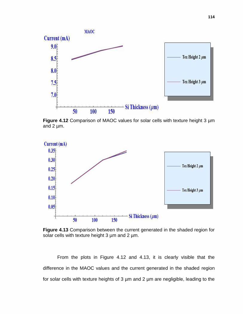
114
Figure 4.12 Comparison of MAOC values for solar cells with texture height 3 µm and 2 µm.
Figure 4.13 Comparison between the current generated in the shaded region for solar cells with texture height 3 µm and 2 µm.
From the plots in Figure 4.12 and 4.13, it is clearly visible that the
difference in the MAOC values and the current generated in the shaded region
for solar cells with texture heights of 3 µm and 2 µm are negligible, leading to the

115
conclusion that the effect of texture height can be ignored while designing the
structure for a solar cell, as long as the texture size is larger than the wavelength
of the incident light.
4.3 Conclusions
The new version of PV Optics has been used to carry out simulations for different
solar cell structures in order to identify their optical performance. Calculations
were carried out for:
various silicon absorber layer thicknesses,
different front metal electrode widths, and
texture heights.
The results for these calculations have also been summarized to give the effect
of each of these parameters on the performance of solar cells.

116
CHAPTER 5
SUMARY OF RESULTS: SOLAR CELL ENCAPSULATED IN A MODULE
5.1 Introduction
Solar cells, by nature, are very brittle and cannot handle a lot of stress. They
have to be packaged in a module, also called solar panels, before installation in
order to make them sturdy enough to endure all stresses during installation and
functioning. Modules also contain an array of solar cells connected together
electrically to give the desired current output. So they contain all the electrical
wiring and connections that would lead to proper current extraction from the
encapsulated array of solar cells. Modules are generally made using the
following constituents:
top glass enclosure,
top encapsulant,
array of solar cells,
a back sheet for support,
a junction box, and
an enclosing fame for mechanical support.
Figure 5.1 shows all these constituents of a solar module and also a
finished solar panel. Sunlight is incident from the top of the module. Hence,
before reaching the surface of the cell, sunlight has to first pass through the glass
and the encapsulant layers. These extra intermediate layers on top of a cell
result in the increase in the reflectance losses in the module compared to a stand

117
alone solar cell. This is accompanied by a saving in further optical losses due to
the light trapping capabilities of the intermediate layers. Figure 5.2 elucidates
both these optical effects clearly. It is of utmost importance that the refractive
indices of the glass layer and the encapsulant layer are matched as closely as
possible in order to inhibit any reflectance loss from the glass-encapsulant
interface. Figure 5.2 takes this refractive index matching into account.
Figure 5.1 The various constituents of a solar module and a solar panel [172].
Figure 5.2 Optical effects in a module.

118
This chapter presents the simulation results of the effect of encapsulation
on the performance of solar cells. The glass and encapsulant thicknesses have
been kept constant for all calculations in order to spot general trends in module
performances depending on the front metal architecture. Table 5.1 spells out the
various properties of the glass and encapsulant layers.
Table 5.1 Properties of glass and encapsulant layers used for simulations
Layer Properties
Glass
Thickness
100 µm
Refractive Index
1.52
Extinction Coefficient
0.0
Encapsulant
Thickness
50 µm
Refractive Index
1.50
Extinction Coefficient
0.0
5.2 Simulation Results
In order to make a systematic study of the effect of encapsulation on the
performance of solar cells, calculations in this chapter are a continuation from
Chapter 4. The cell structures are the same as before with the exception that
glass and encapsulant layers have been added on top. One difference from the
previous chapter is that the effect of texture height, upon encapsulation, has not
been presented here due to the previous observation that this makes no

119
observable difference in the performance of the cell. Another difference is the
addition of calculation results for various finger and busbar heights under
encapsulation. This has been done to investigate whether metal height variation
has any effect on the light trapping characteristics of the glass-air interface.
Two important points have to be noted at the outset in order to make a
meaningful study of the effect of encapsulation. Firstly, as shown in Table 5.1,
refractive indices of the glass and encapsulant materials have a very close
match. This means that, for all practical purposes, there is no optical loss at this
interface. Secondly, for the refractive index of glass used for the calculations, at
normal incidence, there is a direct loss of 4.258% of the incident light at the air-
glass interface. This would lead to the supposition that the total current
generated in a cell encapsulated in a module should be reduced by the same
amount compared to the case with no encapsulation. But as shown in Figure 5.1,
the reduction in current from a solar cell placed in a module would be slightly less
than this value of 4.258% because of the inherent light trapping characteristics of
the module.
5.2.1 Variation in Silicon Absorber Layer Thickness Calculations are presented for thicknesses of 40 µm, 80 µm, 120 µm, and 180
µm. All the other structural parameters have been kept the same as for the case
of without encapsulation for comparison. Table 5.2 summarizes the results of
these calculations. Figures 5.3-5.6 presents all the above results in graphical
form along with the results for only a solar cell to elucidate the effect of
encapsulation of a solar cell.

120
Table 5.2 Summary of calculated results for different absorber layer thicknesses and metal finger with of 100 µm
Silicon Thickness
(µm)
MOAC (A)
Ref. Loss (mA)
Back Metal Abs. Loss
(mA)
Front Metal Abs. Loss (mA)
%age change in MAOC in
module
40
8.13 1209.16 681.31 2.55
0.16
80
8.4 1081.5 552.63 2.59
0.22
120
8.55 993.16 496.46 2.73
0.27
150
8.63
964.82 450.05 2.66 0.295
180
8.72 918.4
411.27 2.47
0.32
Figure 5.3 Plot of MAOC of (a) cell, and (b) module with respect to silicon thickness.

121
.
Figure 5.4 Plots of Reflectance Losses for (a) cell, and (b) module.
Figure 5.5 Plots of Back Metal Losses for (a) cell, and (b) module.
The total current produced in a solar cell upon encapsulation in a module
is always lesser than when un-encapsulated. This change in the current is almost
entirely due to the increase in the reflectance loss of a cell upon encapsulation.
This is borne out of the plots in Figure 5.5 which shows that there is negligible

122
change in back metal loss in a cell upon encapsulation. This can be explained by
taking into account the light trapping properties of a module.
Some of the photons, which have low absorption coefficient in silicon,
upon leaving the cell surface are reflected back in the silicon absorber layer from
the glass-air interface. These reflected photons then add to the overall current in
the module as well as the back metal loss. This aids in keeping the back metal
loss practically the same for a solar cell, within or without a module.
Figure 5.6 Plot of percentage current generated in the shaded region.
Another aspect of encapsulation that is also worth mentioning is the
reduction in the total current generated under the shaded region in a module.
This is simply an artifact of the increase in the reflectance loss from a cell upon
encapsulation due to which less light diffuses into the shaded region of the solar
cell. Figures 5.7 and 5.8 show the photon absorption pattern under the shaded
region of a module with 40 µm silicon thickness to illustrate this point.
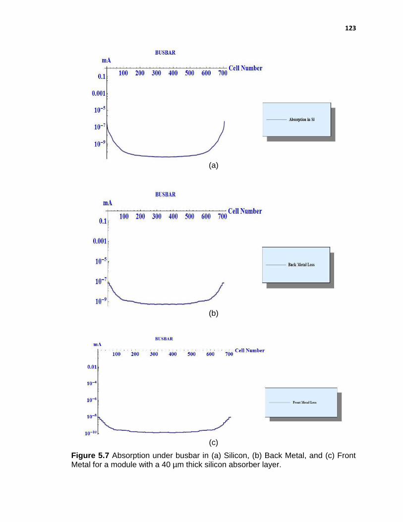
123
(a)
(b)
(c)
Figure 5.7 Absorption under busbar in (a) Silicon, (b) Back Metal, and (c) Front Metal for a module with a 40 µm thick silicon absorber layer.

124
(a)
(b)
(c)
Figure 5.8 Absorption under a finger in (a) Silicon, (b) Back Metal, and (c) Front Metal for a module with a 40 µm thick silicon absorber layer.

125
5.2.2 Variation in Metal Finger Width
As in the last chapter, results of the calculation are presented for three
different metal finger widths of (a) 25 µm, (b) 50 µm, and (c) 75 µm for silicon
thickness of (a) 40 µm, (b) 80 µm, (c) 120 µm, and (d) 180 µm. Tables 5.3-5.5
show the summary of these results. There are two points that are of interest
concerning the results shown above. The first one is to see if a change in metal
finger height makes any difference in the MAOC, the losses or the amount of
current generated in the shaded region in the module. The second point of
interest is to compare the above results with the case of an un-encapsulated
solar cell. Figures 5.9-5.12 show comparative plots for the first point.
Table 5.3 Summary of calculated results for different absorber layer thicknesses and metal finger width of 25 µm
Absorber Layer
Thickness (µm)
Maximum Achievable
Output Current (A)
Reflectance Loss (mA)
Back Metal Absorption Loss (mA)
Front Metal
Absorption Loss (mA)
% age current
generated in the
shaded region
40
8.13 1222.69 683.54 3.98 0.46
80
8.4 1098.13 553.15 3.23 0.53
120
8.55 1011.301 496.58 2.9 0.565
180
8.72 937.44 411.281 2.48 0.605

126
Table 5.4 Summary of calculated results for different absorber layer thicknesses and metal finger width of 50 µm
Absorber Layer
Thickness (µm)
Maximum Achievable
Output Current (A)
Reflectance Loss (mA)
Back Metal Absorption Loss (mA)
Front Metal
Absorption Loss (mA)
% age current
generated in the
shaded region
40
8.13 1212.78 682.52 3.29 0.28
80
8.4 1085.76 553.26 3.22 0.35
120
8.55 998.88 496.63 2.89 0.39
180
8.72 924.76 411.27 2.48 0.44
Table 5.5 Summary of calculated results for different absorber layer thicknesses and metal finger width of 75 µm
Absorber Layer
Thickness (µm)
Maximum Achievable
Output Current (A)
Reflectance Loss (mA)
Back Metal Absorption Loss (mA)
Front Metal
Absorption Loss (mA)
% age current
generated in the
shaded region
40
8.11 1208.02 680.74 2.9 0.202
80
8.36 1080.75 552.01 2.93 0.275
120
8.54 992.8 495.88 2.94 0.32
180
8.69 918.93 410.58 2.5 0.37

127
Figure 5.9 Plot of MAOC values for module with respect to silicon thickness for metal finger width of (a) 100 µm, (b) 75 µm, (c) 50 µm, and (d) 25 µm.
Figure 5.10 Plot of reflectance loss values for module with respect to silicon thickness for metal finger width of (a) 100 µm, (b) 75 µm, (c) 50 µm, and (d) 25 µm.
Figure 5.11 Plot of reflectance loss values for module with respect to silicon thickness for metal finger width of (a) 100 µm, (b) 75 µm, (c) 50 µm, and (d) 25 µm.

128
Figure 5.12 Plot of percentage current produced in shaded region for module with respect to silicon thickness for metal finger width of (a) 100 µm, (b) 75 µm, (c) 50 µm, and (d) 25 µm.
Figure 5.13 Plot of MAOC values for cell and module with respect to silicon thickness for metal finger width of (a) 100 µm, (b) 75 µm, (c) 50 µm, and (d) 25 µm.

129
Figures 5.12-5.14 clearly show that there is negligible change in the
MAOC values as well as the reflectance and the back metal loss values upon
varying the width of the metal fingers. It would be pertinent to remember here
that while changing their width, the total area under shading was kept constant to
facilitate a meaningful comparison. This means that, as the width decreases, the
distances between the metal fingers decrease as well. Figure 5.10 shows the
plots of the current generated in the shaded region for the various widths of metal
fingers in a module.
Figure 5.13 shows the clear segregation of the cell and module MAOC
values for different metal finger widths. Figure 5.14 shows a similar plot for
reflectance losses for cell and module for reference.
Figure 5.14 Plot of reflectance loss for cell and module with respect to silicon thickness for metal finger width of (a) 100 µm, (b) 75 µm, (c) 50 µm, and (d) 25 µm.
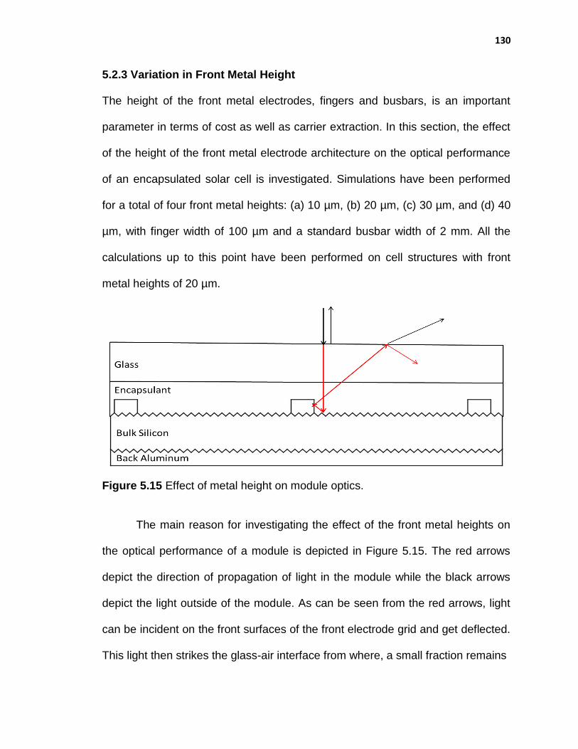
130
5.2.3 Variation in Front Metal Height The height of the front metal electrodes, fingers and busbars, is an important
parameter in terms of cost as well as carrier extraction. In this section, the effect
of the height of the front metal electrode architecture on the optical performance
of an encapsulated solar cell is investigated. Simulations have been performed
for a total of four front metal heights: (a) 10 µm, (b) 20 µm, (c) 30 µm, and (d) 40
µm, with finger width of 100 µm and a standard busbar width of 2 mm. All the
calculations up to this point have been performed on cell structures with front
metal heights of 20 µm.
Figure 5.15 Effect of metal height on module optics.
The main reason for investigating the effect of the front metal heights on
the optical performance of a module is depicted in Figure 5.15. The red arrows
depict the direction of propagation of light in the module while the black arrows
depict the light outside of the module. As can be seen from the red arrows, light
can be incident on the front surfaces of the front electrode grid and get deflected.
This light then strikes the glass-air interface from where, a small fraction remains

131
Table 5.6 Summary of calculated results for different absorber layer thicknesses and metal finger height of 10 µm
Absorber Layer
Thickness (µm)
Maximum Achievable
Output Current (A)
Reflectance Loss (mA)
Back Metal Absorption Loss (mA)
Front Metal
Absorption Loss (mA)
% age current
generated in the
shaded region
40
8.13 1209.251 681.34 2.56 0.16
80
8.4 1081.51 552.69 2.61 0.22
120
8.55 993.11 496.52 2.76 0.27
180
8.72 918.43 411.27 2.47 0.32
Table 5.7 Summary of calculated results for different absorber layer thicknesses and metal finger height of 30 µm
Absorber Layer
Thickness (µm)
Maximum Achievable
Output Current (A)
Reflectance Loss (mA)
Back Metal Absorption Loss (mA)
Front Metal
Absorption Loss (mA)
% age current
generated in the
shaded region
40
8.13 1209.01 681.27 2.56 0.16
80
8.4 1081.29 552.62 2.61 0.22
120
8.55 992.99 496.43 2.76 0.27
180
8.72 918.33 411.3 2.47 0.32
inside the module while the rest is lost as reflectance loss. The amount of light
incident on the front metal is related to their height. This might have an effect on
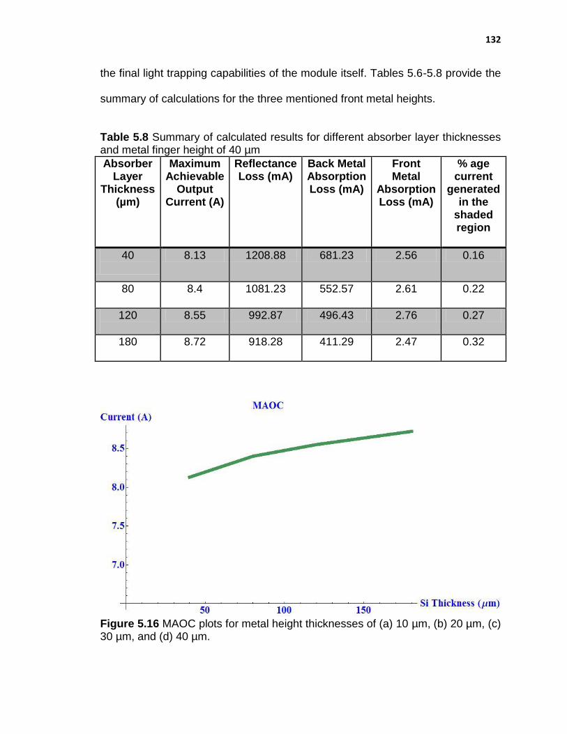
132
the final light trapping capabilities of the module itself. Tables 5.6-5.8 provide the
summary of calculations for the three mentioned front metal heights.
Table 5.8 Summary of calculated results for different absorber layer thicknesses and metal finger height of 40 µm
Absorber Layer
Thickness (µm)
Maximum Achievable
Output Current (A)
Reflectance Loss (mA)
Back Metal Absorption Loss (mA)
Front Metal
Absorption Loss (mA)
% age current
generated in the
shaded region
40
8.13 1208.88 681.23 2.56 0.16
80
8.4 1081.23 552.57 2.61 0.22
120
8.55 992.87 496.43 2.76 0.27
180
8.72 918.28 411.29 2.47 0.32
Figure 5.16 MAOC plots for metal height thicknesses of (a) 10 µm, (b) 20 µm, (c) 30 µm, and (d) 40 µm.

133
It is again interesting to note that the MAOC values for various front metal
heights for each silicon absorber layer thickness is unchanging to second
decimal. Any change in current due to the heights in silver metal is only beyond
this point. Silver, being such a good reflector, does not absorb a huge amount
light that is incident on it. This again stresses the point that the optical effects,
due to the above mentioned changes in solar cell structure, are minimal and
hence, the electrical properties take precedence over the optical effects.
Figure 5.17 Reflectance loss plots for metal height thickness of (a) 10 µm, (b) 20 µm, (c) 30 µm, and (d) 40 µm.
Figure 5.18 Back metal loss plots for metal height thickness of (a) 10 µm, (b) 20 µm, (c) 30 µm, and (d) 40 µm.

134
Figure 5.19 Percentage current generated in the shaded region of a module plots for metal height thickness of (a) 10 µm, (b) 20 µm, (c) 30 µm, and (d) 40 µm.
Figures 5.13-5.16 also show that the effect of the front metal is minimal on
the optical performance of solar cells.
5.3 Conclusions
All the results of simulations using the new ray tracing C++ code for PV Optics
4.0 have been presented in this Chapter. The structural parameters used for
these calculations have been kept the same as in Chapter 4 except for the
change that the cells have been encapsulated in a module. Calculations have
also been done to see the effect of front metal height on the optical performance
of a module. The results show that there is minimal effect of the front metal
electrode architecture used presently in commercial single crystal (100) silicon
solar cell modules. This emphasizes the fact that carrier transport is the main

135
factor that should be taken into account while designing the front metal electrode
architecture in cells and modules.

136
CHAPTER 6
CONCLUSIONS AND FUTURE DIRECTIONS
The objective of this dissertation was to develop a new and complete model to
incorporate the front metal electrode architecture that are used in commercial
single crystal (100) orientation silicon solar cells for optical simulations. This new
model was implemented in a computer program written in C++ to be added as a
new module to PV Optics Ver. 4.0. Investigations have been carried out on
various front metal architecture and solar cell structures to study their effect on
the performance of solar cells from a purely optics point of view.
6.1 Conclusions on Front Metal Architecture Modeling
It has been established during the course of this research that a simpler 2D
structural as well as procedural model can be used to carry out simulations on a
3D structure of single crystal (100) oriented silicon solar cells. Reducing such a
complex 3D model into a 2D model has the following advantages:
The 2D model has the same accuracy as the corresponding 3D model,
This new model reduces the calculation time and the computing budget for a finished 156 mm X 156 mm solar cell by at least one order of magnitude from the corresponding 3D computation.
The computational budget required to do the optical simulations using the new model and computer program is also substantially reduced.
The use of this model to study the effect of the front metal architecture of a
solar cell on its performance has shown some very interesting results. The total
current generated in a finished 156 mm X 156 mm solar cell increases with the

137
subsequent increase in the silicon absorber layer thickness. It is found that the
increase in current, upon increasing the silicon thickness from 40 µm to 180 µm
(change in thickness of 350%), results in the increase in the MAOC by only
6.855%. This is a clear indicator that use of better light trapping and wafer
handling technologies will lead to a decrease in silicon wafer thickness for solar
cell production. The potential to cut production costs due to this is immense and
can eventually lead solar energy to become competitive with other forms of
energy in the near future.
This research also establishes, for the first time, that there is a very
minimal effect of the front metal architecture on the performance of commercial
single crystal silicon solar cell structures. Solar cell designers have a simpler task
with one less variable, i.e., optical design, to come up with new solar cell
architecture. But it is also relevant to mention that the main challenge in
designing solar cells would be to keep the shaded region as small as possible to
be able to use the maximum volume of the device for current generation.
It has been firmly established that, for optical calculations, 2D models can
be used with great accuracy to tackle a 3D problem. This work should act as a
catalyst for the incorporation of many other front and back metal electrode
architectures for optical simulations. The effect of other metal geometries and
architectures are still open to investigation.

138
6.2 Future Directions
This work should be extended further in order to study the effect of novel front
and back metal electrode structures on solar cell performance. Following is the
scope for expanding and improving the present research:
1) this model can be expanded to include texture etched multicrystalline silicon solar cells; No such model exists as yet,
2) introduction of novel light trapping technologies, discussed in Chapter 3, into the existing model;
3) extension of this model to also handle thin film solar cells;
4) introduction of new metal architectures such as inter-digitated contacts in the existing model;
5) incorporate parallel processing into the existing C++ code to further reduce the simulation time.

139
REFERENCES
1. D.O.E., U.S. The History of Solar. 2012 [cited 2012 11/06]; Available from: http://www1.eere.energy.gov/solar/pdfs/solar_timeline.pdf.
2. M.Wolf, Historical Development of Solar Cells. Solar Cells, ed. C.E.
Backus1976, New York: IEEE Press. 3. A.Carr, et al. How are Solar Cells made? 1999 [cited 2012 11/06];
Available from: http://www.esdalcollege.nl/eos/vakken/na/zonnecel.htm. 4. B.Averill and P.Eldredge. General Chemistry: Principles, Patterns, and
Applications. 2007 [cited 2012 11/05]; Available from: http://images.flatworldknowledge.com/averillfwk/averillfwk-fig12_027.jpg.
5. W.U.Boeglin. P-N Junction. 2011 [cited 2012 11/05]; Available from:
http://wanda.fiu.edu/teaching/courses/Modern_lab_manual/pn_junction.html.
6. N.W.Ashcroft and N.D.Mermin, Solid State Physics, 1976, Thompson
learning. 7. L.V.Azaroff and J.J.Brophy, Electronic Processes in Materials1963:
McGraw-Hill. 8. S.Wang, Solid State Electronics, 1996, McGraw-Hill: New York. 9. AllAboutCircuits.com. Diodes. 2012 [cited 2012 11/05]; Available from:
http://solarwiki.ucdavis.edu/The_Science_of_Solar/1._Basics/A._Introductory_Physics_for_Solar_Application/II._Electricity/5._Diodes.
10. D.R.Williams. Sun Fact Sheet. 2012 [cited 2012 11/05]; Available from:
http://nssdc.gsfc.nasa.gov/planetary/factsheet/sunfact.html. 11. M.P.Thekackara, The Solar Constant and the Solar Spectrum Measured
form a Research Aircraft, 1970, NASA Technical Report No. R-351. 12. M.A.Green, Solar Cells: Operating Principles, Technology, and System
Applications 1982, Prentice-Hall: New Jersey. p. 5. 13. P.R.Gast, Solar Radiation, in Handbook of Geophysics, C.F. Campen,
Editor 1960, Macmillan: New York. p. 14-16. 14. Gast, P.R., Solar Radiation, in Handbook of Geophysics, C.F. Campen,
Editor 1960, Macmillan: New York. p. 16-30.

140
15. F-J.Haug. Irradiation spectrum. [cited 2012 11/05]; Available from: http://www.superstrate.net/pv/illumination/spectrum.html.
16. Terrestrial Photovoltaic Measurement Procedure, 1977, NASA Report
ERDA/NASA/1022-77/16. 17. Principal Conclusion of the American Physical Society Study Group on
Solar Photovoltaic Energy Conversion, 1979, American Physical Society: New York.
18. D.M.Chapin, C.S.Fuller, and G.L.Pearson, A New Silicon p-n Junction
Photocell for Converting Solar Radiation into Electrical Power. Journal of Applied Physics, 1954. 25(5): p. 676.
19. M.S.Green, Solar Cells, in Modern Semiconductor Device Physics,
S.M.Sze, Editor 1998, Wiley Interscience: New York. 20. M.A.Green, Thin-film solar cells: review of materials, technologies and
commercial status. J Mater Sci: Mater Electron, 2007. 18: p. S15–S19. 21. A.V.Shah, R.Platz, and H.Keppner, Thin-film silicon solar cells: A review
and selected trends. Solar Energy Materials and Solar Cells, 1995. 38(1-4): p. 501-520.
22. M.Gratzel, Dye-sensitized solar cells. Jounal of Photochemistry and
Photobiology C: Photochemistry Reviews, 2003. 4(2): p. 145-153. 23. M.Gratzel, Solar Energy Conversion by Dye-Sensitized Photovoltaic Cells.
Inorg. Chem., 2005. 44(20): p. 6841-6851. 24. K.L.Chopra, P.D.Paulson, and V.Dutta, Thin-Film Solar Cells: An
overview. Prog. Photovolt: Res. Appl., 2004. 12(2-3): p. 69-92. 25. M.Pagliaro, R.Ciriminna, and G.Palmisano, Flexible Solar Cells.
ChemSusChem, 2008. 1(11): p. 880-891. 26. A.Romeo, et al., Development of Thin-film Cu(In,Ga)Se2 and CdTe Solar
Cells. Prog. Photovolt: Res. Appl., 2004. 12(2-3): p. 93-111. 27. X.Wu, High-efficiency polycrystalline CdTe thin-film solarcells. Solar
Energy, 2004. 77(6): p. 803-814. 28. A.Shah, et al., Photovoltaic Technology: The Case for Thin-Film Solar
Cells. Science, 1999. 285(5428): p. 692-698.
141
29. J.H.Bang and P.V.Kamat, Quantum Dot Sensitized Solar Cells. A Tale of Two Semiconductor Nanocrystals: CdSe and CdTe. ACS Nano, 2009. 3(6): p. 1467–1476.
30. R.W.Birkmire and E.Eser, POLYCRYSTALLINE THIN FILM SOLAR
CELLS:Present Status and Future Potential. Annual Review of Materials Science, 1997. 27: p. 625-653.
31. Dobson, K.D., et al., Stability of CdTe/CdS thin-film solarcells. Solar
Energy Materials and Solar Cells, 2000. 62(3). 32. S.M.Sze, Semiconductor Devices: Physics and Technology, 1985, John
Wiley & Sons. p. 320. 33. solar-is-future.com. How Photovoltaics Work: From Light to Electricity.
2012 [cited 2012 11/05]; Available from: http://www.solar-is-future.com/solar-energy-source/how-photovoltaics-work/from-light-to-electricity/index.html.
34. A.B.Banful, A.Liu, and E.Rodriguez. How a solar cell works. 2002 [cited
2012 11/06]; Available from: http://stuff.mit.edu/afs/athena.mit.edu/course/3/3.082/www/team2_f02/Pages/background.html.
35. Key Solar Cell Parameters and Measurement Techniques. 2012 [cited
2012 11/06]; Available from: http://www.keithley.nl/solar_cell. 36. M.A.Green, Solar Cells: Operating Principles, Technology, and System
Applications 1982, New Jersey: Prentice-Hall. 37. M.Born and E.Wolf, Principles of Optics, 1999, Cambridge University
Press. p. 1-3. 38. M.Born and E.Wolf, Principles of Optics, 1999, Cambridge University
Press. p. 11. 39. M.Born and E.Wolf, Principles of Optics, 1999, Cambridge University
Press. p. 14-25. 40. A representation of a plane wave's electric field shown from an oblique
angle. 2010 [cited 2012 11/05]; Available from: http://commons.wikimedia.org/wiki/File:Plane_Wave_Oblique_View.jpg.
41. M.Born and E.Wolf, Principles of Optics, 1999, Cambridge University
Press. p. 38-40.

142
42. Diagram of reflection and refraction. 2012 [cited 2011 11/06]; Available from: http://www.glossary.oilfield.slb.com/DisplayImage.cfm?ID=255.
43. M.Born and E.Wolf, Principles of Optics, 1999, Cambridge University
Press. p. 40-43. 44. M.Born and E.Wolf, Principles of Optics, 1999, Cambridge University
Press. p. 49-53. 45. M.Born and E.Wolf, Principles of Optics, 1999, Cambridge University
Press. p. 736. 46. M.Born and E.Wolf, Principles of Optics, 1999, Cambridge University
Press. p. 737. 47. M.Born and E.Wolf, Principles of Optics, 1999, Cambridge University
Press. p. 739-749. 48. A.S.Glassner, An Introduction to Ray tracing 1989: Morgan Kaufmann. 49. W.J.Smith, Modern Optical Engineering. 4 ed2008: McGraw-Hill. 50. B.Sopori, PV Optics: A software package for solar cell and module design,
in Optical Modeling and Measurements for Solar Energy Systems2007, SPIE: San Diego, CA. p. 665206
51. Ray-Tracing. 2012 [cited 2012 11/06]; Available from: http://www.ice.rwth-
aachen.de/research/tools-projects/grace/ray-traycing/. 52. F.J.Beck, A.Polman, and K.R.Catchpole, Tunable light trapping for solar
cells using localized surface plasmons. Journal of Applied Physics, 2009. 105(11): p. 114310- 114317.
53. A.W.Smith and A. Rohatgi, Raytracing analysis of the inverted pyramid
texturing geometry for high efficiency silicon solarcells. Solar Energy Materials and Solar Cells, 1993. 29(1): p. 37–49.
54. M.A.Green, Lambertian Light Trapping in Textured Solar Cells and Light-
Emitting Diodes: Analytical Solutions. Prog. Photovolt: Res. Appl. , 2002. 10: p. 235–241.
55. P.Campbell and M.A.Green, Light trapping properties of pyramidally
textured surfaces. Journal of Applied Physics, 1987. 62: p. 243.

143
56. B.L.Sopori, et al., Light-Trapping in a-Si Solar Cells: A Summary of the Results from PV Optics, in National Center for Photovoltaics Program Review Meeting 1998, NREL: Denver, CO.
57. A.E.St.John, Multiple internal reflection structure in a silicon detector
which is obtained by sandblasting, 1969: U.S. Patent No. 3,487,223. 58. O.Krumpholz and S.Maslowski, Schnelle Photodioden mit
wellenlagnenunabhangigen Demodulatonseigenschaften. Z. Angew. Phys., 1968. 25: p. 156.
59. B.Sopori, et al., A new method for rapid measurement of orientations and
sizes of grains in multicrystalline silicon wafers, in 37th IEEE PVSC 2011, IEEE: Seattle, WA. p. 001680- 001685
60. J.A.Rand and P.A.Basore, Light-trapping in silicon solar cells-experimental
results and analysis, in 22nd IEEE PVSC1991. p. 192-197. 61. P.Campbell, Light trapping in textured solar-cells. Solar Energy Materials
1990. 21: p. 165-172. 62. P.Campbell, Enhancement of light-absorbing from randomizing and
geometric textures. J. Opt. Soc. Am. B, 1993. 10: p. 2410-2415. 63. P.Campbell and M.A.Green, High performance light trapping textures for
monocrystalline silicon solar cells. Solar Energy Materials and Solar Cells, 2001. 65: p. 369-375.
64. V.Y.Yerokhov, et al., Cost-effective methods of texturing for silicon solar
cells. Solar Energy Materials and Solar Cells, 2002. 72: p. 291-298. 65. J.D.Hylton, A.R.Burgers, and W.C.Sinke, Light trapping in alkaline texture
etched crystalline silicon wafers, in 16th European Photovoltaic Solar Energy Conference, H. Scheer, et al., Editors. 2000: Glasgow, UK. p. 1434-1437.
66. J.W.Mueller, A.Metz, and R.Hezel. A new and simple approach for
fabricating inverted pyramids on crystalline silicon solar cells. in 17th European Photovoltaic Solar Energy Conference. 2001. Munich.
67. P.Panek, M.Lipinski, and J.Dutkiewicz, Texturization of multicrystalline
silicon by wet chemical etching for silicon solar cells. Journal of Material Science, 2005. 40(6): p. 1459-1463.
68. D.R.Turner, Electropolishing of siilcon in hydroflouric acid solutions.
Journal of the Electrochemical Society, 1958. 105: p. 402-408.

144
69. B.Schwartz and H.Robbins, Chemical etching of silicon, Part I, The system HF, HNO3, H2O, HC2H3O2. Journal of Electrochemical Society, 1959. 106(6): p. 505-508.
70. K.E.Bean, Anisotropic etching of silicon Electron Devices, IEEE
Transactions, 1978. 25(10): p. 1185-1193. 71. P.J.Holmes, The Electrochemistry of Semiconductors, 1962, Academic
Press: London. p. 329. 72. W.L.Bailey, et al., Texture Etching of Silicon: Method, 1979: U.S. Patent
No. 4,137,123. 73. H.Seidel, et al., Anisotropic Etching of Crystalline Silicon in Alkaline
Solutions I. Orientation Dependence and Behavior of Passivation Layers. Journal of Electrochemical Society, 1990. 137(11): p. 3612-3626.
74. P.Papet, et al., Pyramidal texturing of silicon solar cell with TMAH
chemical anisotropic etching. Solar Energy Materials and Solar Cells, 2005. 90(15): p. 2319–2328.
75. A.J.Nijdam, et al., Etching of silicon in alkaline solutions: a critical look at
the {111} minimum. Journal of Crystal Growth, 1999. 198/199: p. 430-434. 76. Theory, technology, diagnostics and application of silicon solar cells.
[cited 2012 11/10]; Available from: http://cellstester.narod.ru/technology_en.html.
77. C.Honsberg and S.Bowden. Surface Texturing. [cited 2012 11/08];
Available from: http://www.pveducation.org/pvcdrom/design/surface-texturing.
78. E.D.Palik, H.F.Gray, and P.B.Klein, A Raman Study of Etching Silicon in
Aqueous KOH. J. Electrochem. Soc. , 1983. 130: p. 956-959. 79. V.A.Burrows, et al., Infrared spectroscopy of Si (111) surfaces after HF
treatment: hydrogen termination and surface morphology. Appl. Phys. Lett., 1998. 53: p. 998-1000.
80. G.S.Higashi, et al., Ideal hydrogen termination of the Si (111) surface.
Appl. Phys. Lett., 1990. 56: p. 656-658. 81. N.Hirashita, et al., Effects of surface hydrogen on the air oxidation at room
temperature of HF-treated Si (100) surfaces. Appl. Phys. Lett., 1990. 56: p. 451-453.

145
82. R.M.Finne and D.L.Klein, A Water-Amine-Complexing Agent System for “Etching Silicon. J. Electrochem. Soc., 1967. 114(9): p. 965-970.
83. E.D.Palik, V.M.Bermudez, and O.J.Glembocki, Ellipsometric Study of OrientationDependent Etching of Silicon in Aqueous KOH. J. Electrochem. Soc. (Solid-State Science & Technology), 1998. 132: p. 871-884.
84. W-J.Cho, W-K.Chin, and C-T.Kuo, Effect of alcoholic moderators on
anisotropic etching of silicon in aqueous potassium hydroxide solutions. Sensors and Actuators A: Physical, 2004. 118(2): p. 357-368.
85. J.B.Price, Anisotropic Etching of Silicon with KOH-H20-Isopropyl Alcohol.
Semiconductor Silicon, ed. R.R. Burfess and H.R. Huff1973, Princeton, NJ: The Electrochemical Society Softbound Proceedings Series.
86. J.D.Hylton, Light coupling and light trapping in alkaline etched
multicrystalline silicon wafers for solar cells, in Department of Physics 2006, Universitiet Utrecht: Netherlands.
87. Z-f.Zhou, et al., A cellular automaton-based simulator for silicon
anisotropic etching processes considering high index planes. J. Micromech. Microeng., 2007. 17: p. S38–S49.
88. B.Mills, Ball-and-stick model of the unit cell of silicon, Silicon-unit-cell-3D-
balls.png, Editor 2007, Wikipedia: USA. 89. P.Maycock, Renewable Energy World, 2003. 7(PV marked update): p. 84-
111. 90. D.L.King and M.E.Buck, Experimental Optimisation of an Anisotropic
Etching Process for Random Texturisation of Silicon Solar Cells, in 22nd IEEE PVSC1991. p. 303-308.
91. R.Einhaus, et al., Isotropic texturing of multicrystalline silicon wafers with
acidic texturing solutions, in 26th IEEE PVSC1997: Anaheim. p. 167-170. 92. M.J.Stocks, A.J.Carr, and A.W.Blakers, Texturing of polycrystalline silicon,
in 1st WCPEC1994: Hawaii. p. 1551-1554 93. M.J.Stocks, A.J.Carr, and A.W.Blakers, Texturing of polycrystalline silicon.
Solar Energy Materials and Solar Cells, 1996. 40: p. 33-42. 94. H.Robbins and B.Schwartz, Chemical Etching of Silicon: II . The System
HF, HNO3, H2O, and HC2H3O2. J.Electrochem. Soc., 1960. 107(2): p. 108-111

146
95. B.Schwartz and H.Robbins, Chemical Etching of Silicon: III . A Temperature Study in the Acid System. J. Electrochem. Soc., 1961. 108(4): p. 365-372.
96. B.Schwartz and H.Robbins, Chemical Etching of Silicon: IV . Etching
Technology. J. Electrochem. Soc., 1976. 123(12): p. 1903-1909. 97. S.Zhou, et al., Experimental study on the elimination of over-plating
problems in industrial manufacturing of large-area acidic-textured laser-doped multicrystalline solar cells. Solar Energy Materials and Solar Cells, 2013. 108: p. 44-49.
98. T.Nunoi, et al., Cast polycrystalline silicon solar cell with grooved surface,
in 21st IEEE PVSC1990: Kissimmee p. 664-665. 99. G.Willeke, et al., A simple and effective light trapping technique for
polycrystalline silicon solar cells. Solar Energy Materials and Solar Cells, 1992. 26: p. 345-356.
100. H.Nakaya, et al., Polycrystalline silicon solar cells with V-grooved surface.
Solar Energy Materials and Solar Cells, 1994. 34: p. 219-225. 101. Y.Hayashi, et al., in 10th EC PVSEC 1991, Kluwer Academic Publishers:
Lisbon. p. 254. 102. M.B.Rabha, et al., Optoelectronic enhancement of monocrystalline silicon
solar cells by porous silicon-assisted mechanical grooving. Phus. Status Solidi C, 2011. 8(3): p. 887-890.
103. W.A.Nositschka, et al., Texturisation of multicyrstalline silicon wafers for
solar cells by reactive ion etching through colloidal masks. Solar Energy Materials & Solar Cells, 2003. 76: p. 155-166.
104. H.Jansen, et al., A survey on the reactive ion etching of silicon in
microtechnology. J. Micromech. Microeng., 1996. 6: p. 14-28. 105. H.Jansen, et al., The black silicon method: a universal method for
determining the parameter setting of a fluorine-based reactive ion etcher in deep silicon trench etching with profile control. J. Micromech. Micoreng. , 1995. 5: p. 115-120.
106. A.R.Burgers and J.H.Bultman, SIlicon Solar Cells Textured By Reactive
Ion Etching With Natural Lithography, in 16th European Photovoltaic Solar Energy Conference and Exhibition2000: Glasgow.
147
107. Dry etching. [cited 2012 11/10]; Available from: https://http://www.mems-exchange.org/MEMS/processes/etch.html.
108. H.F.Winters, The role of chemisorption in plasma etching. J. Appl. Phys. ,
1978. 49: p. 5165-5170. 109. K.-s.Lee, et al., Damage-free reactive ion etch for high-efficiency large-
area multi-crystalline silicon solar cells. Solar Energy Materials and Solar Cells, 2011. 95(1): p. 66–68.
110. G.Willeke and P.Faith, Texturisation methods for multicrystalline silicon
solar cells, in 13th EPVSEC1995: Nice. p. 399-402. 111. J.C.Zolper, et al., Applied Physics Letters. 16.7% efficient, laser textured,
buried contact, polycrystalline silicon solar cell, 1989. 55(22): p. 2363-2365.
112. M.Abbott and J.Cotter, Optical and Electrical Properties of Laser Texturing for High-efficiency Solar Cells. Prog. Photovolt: Res. Appl., 2006. 14: p. 225-235.
113. B.K.Nayak, V.V.Iyengar, and M.C.Gupta, Efficient light trapping in silicon
solar cells by ultrafast-laser-induced self-assembled micro/nano structures. Prog. Photovolt: Res. Appl., 2011. 19: p. 631-639.
114. T-H.Her, et al., Microstructuring of silicon with femtosecond laser pulses.
Appl. Phys. Lett., 1998. 73(12): p. 1673-1675. 115. A.J.Pedraza, J.D.Fowlkes, and D.H.Lowndes, Silicon micro-column arrays
grown by nanosecond pulsed-excimer laser irradiation. Appl. Phys. Lett., 1999. 74(16): p. 2322-2324.
116. B.K.Nayak, M.C.Gupta, and K.W.Kolasinski, Ultrafast-laser-assisted
chemical restructuring of silicon and germanium surfaces. Applied Surface Science, 2007. 253(15): p. 6580-6583.
117. M.Halbwax, et al., Micro and nano-structuration of silicon by femto-secon
laser: application to silicon photovoltaic cells fabrication. Thin Solid Films, 2008. 516(20): p. 6791-6795.
118. M.D.Abbott, et al., Laser-induced defects in crystalline silicon solar cells,
in 31st IEEE Photovoltaic Specialist ConferenceJanuary 2005: Orlando. p. 1241-1244.
119. K-R.Kima, et al., UV laser direct texturing for high efficiency
multicrystalline silicon solar cell. Applied Surface Science, 2012.

148
120. Using Nanotechnology to Improve Performance of Solar Cell. 2008 [cited 2012 10/11]; Available from: http://www.azonano.com/news.aspx?newsID=7055.
121. M.A.Green, in High Efficiency Solar Cells 1987, Trans Tech:
Aedermannsdorf, Switzerland/Brookfield, VT. p. 70. 122. J.Nelson, in The Physics of Solar Cells 2003, Imperial College: London. p.
279 and 282. 123. E.Hecht, The Diffraction Grating, in Optics1998, Addison Wesley
Longman: Reading, MA. p. 465. 124. C.Heine and R.H.Morf, Submicrometer gratings for solar energy
applications. Applied Optics, 1995. 34(14): p. 2476-2482. 125. C.Eisele, E.Nebel, and M.Stutzmann, Periodic light coupler gratings in
amorphous thin film solar cells. J. Appl. Phys., 2001. 89: p. 7722-7726. 126. F.Llopis and I.Tobías, The role of rear surface in thin silicon solar cells.
Solar Energy Materials and Solar Cells, 2005. 87(1-4): p. 481-492. 127. J.D.Joannopoulos, et al., Photonic Crystals: Modelling the Flow of Light.
2nd ed2007, Princeton and Oxford: Princeton University Press. 128. E.Yablonovitch, Inhibited Spontaneous Emission in Solid-State Physics
and Electronics Physical Review Letters, 1987. 58(20): p. 2059-2062. 129. S.John, Strong localization of photons in certain disordered dielectric
superlattices. Physical Review Letters, 1987. 58(23): p. 2486–2489. 130. R.B.Wehrspohn and J.Upping, 3D photonic crystals for photon
management in solar cells. J. Opt. , 2012. 14: p. 024003 (9pp). 131. D.C.Johnson, et al., Advances in Bragg stack quantum well solar cells.
Solar Energy Materials and Solar Cells, 2005. 87(1-4): p. 169-179. 132. M.Z.Shvarts, et al., Radiation resistant AlGaAs/GaAs concentrator solar
cells with internal Bragg reflector. Solar Energy Materials and Solar Cells, 2001. 68(1): p. 105-122.
133. L.Zeng, et al., Efficiency enhancement in Si solar cells by textured
photonic crystal back reflector. Appl. Phys. Lett., 2006. 89(11): p. 111111-111113.

149
134. Enhancement of Spontaneous Emission in Microcavities, in Vertical-Cavity Surface-Emitting Lasers: Design, Fabrication, Characerization, and Applications, C.W. Wilmsen, H. Temkin, and L.A. Coldren, Editors. 1999, Cambridge University Press: Cambridge. p. 72.
135. P.Bermel, et al., Improving thin-film cyrstalline silicon solar cell efficiencies
with photonic crystals. Optics Express, 2007. 15(25): p. 16986-14000. 136. S.Nie and R.Emory, Probing single molecules and single nanoparticles by
surface-enhanced Raman scattering. Science, 1997. 275: p. 1102-1106. 137. M.Moskovits, Surface-enhanced spectroscopy. Rev. Mod. Phys., 1985.
57(3): p. 783-826. 138. H.R.Stuart and D.G.Hall, Island size effect in nanoparticle-enhanced
photodetectors. Appl. Phys. Lett., 1998. 73(26): p. 3815-3817. 139. D.M.Schaadt, B.Feng, and E.T.Yu, Enhanced semiconductor optical
absorption via surface plasmon excitation in metal nanoparticles. Appl. Phys. Lett., 2005. 86(6): p. 063106-063108.
140. D.Derkacs, et al., Improved performance of amorphous silicon solar cells
via scattering from surface plasmon polaritons in nearby metallic nanoparticles. Appl. Phys. Lett., 2006. 89(9): p. 093103-093105.
141. M.A.Green and S.Pillai, Harnessing plasmonics for solar cells. Nature
Photonics, 2012. 6: p. 130–132. 142. H.Dai, et al., Effective light trapping enhancement by plasmonic Ag
nanoparticles on silicon pyramid surface. Optics Express, 2012. 7(9): p. A502-A509.
143. K.R.Catchpole and A.Polman, Plasmonic solar cells. Optics Express,
2008. 16(26): p. 21793-21800. 144. D.A.Clugston and P.A.Basore, PC1D version 5: 32-bit solar cell modeling
on personal computers, in 26th IEEE PVSC 1997: Anaheim, CA. p. 207-210.
145. R.Stangl, M.Kriegel, and M.Schmidt. AFORS-HET, Version 2.2, A
numerical Computer Program for Simulation of Heterojunction Solar Cells and Measurements. in Photovoltaic Energy Conversion, Conference Record of the 2006 IEEE 4th World Conference 2006. IEEE.
146. R.Stangl, C.Leendertz, and J.Haschke, Numerical simulation of solar and
solar cell characterization methods: the open source on demand program

150
AFORS-HET, in Solar Energy, INTECH, R.D.Rugescu, Editor 2010: Croatia. p. 319-352.\
147. D.Thorp and S.R.Wenham, Ray-tracing of arbitrary surface textures for light-trapping in thin silicon solar cells. Solar Energy Materials and Solar Cells, 1997. 48: p. 295-301.
148. R.Brendel. SUNRAYS: A versatile ray tracing program for photovoltaic
community. in 12th EPVSEC. 1994. Amsterdam. 149. A.W.Smith, A.Rohatgi, and S.C.Neel, Texture: A ray tracing program for
the photovoltaic community, in 21st IEEE PVSC1990, IEEE: Kissimmee, FL. p. 426-43.
150. CROSSLIGHT. APSYS. 2011 [cited 2012 11/11]; Available from:
http://crosslight.com/products/apsys.shtml. 151. Z.Q.Li, Y.G.Xiao, and Z.S.Li. Modeling of multi-juntion solar cells by
Crosslight APSYS. in SPIE. 2006. 152. D.Redfield, Multiple-pass thin-film silicon solar cell. Appl. Phys. Lett.,
1974. 25(11): p. 647-648. 153. E.Yablonovitch, Statistical ray optics. Opt. Soc. Am., 1982. 72(7): p. 899-
907. 154. R.J.Roedel and P.M.Holm, The design of anisotropically etched III-V solar
cells. Solar cells, 1984. 11(3): p. 221-239. 155. A.Wang, J.Zhao, and M.A.Green, 24% efficient silicon solar cells. Appl.
Phys. Lett., 1990. 57(6): p. 602-604. 156. R.Brendel, Coupling of light into mechanically textured silicon solar cells:
A ray tracing study. Prog. Photovolt: Res. Appl., 1995. 3(1): p. 25-38. 157. D.O.E., U.S. Industry Awards. 2012 [cited 2012 11/11]; Available from:
www1.eere.energy.gov/solar/sunshot/accomplishments.html. 158. B.L.Sopori, et al., Modeling Emissivity of Rough andTextured Silicon
Wafers. Journal of Electronic Materials, 1998. 27(12): p. 1341-1346. 159. Y.Nishimoto, T.Ishihara, and K.Namba, Investigation of Acidic
Texturization for Multicrystalline Silicon Solar Cells. J. Electrochem. Soc., 1999. 146(2): p. 457-461.

151
160. J.M.Rodriguez, I.Tobias, and A.Luque, Random pyramidal texture modelling. Solar Energy Materials and Solar Cells, 1995. 45(3): p. 241-253.
161. S.C.Baker-Finch and K.R.McIntosh, Reflection of normally incident light from silicon solar cells with pyramidal texture. Prog. Photovolt: Res. Appl., 2011. 19(4): p. 406-413.
162. B.Sopori, et al., An Optical Technique for Measurement of Grain
Orientation and Sizes in Multicrystalline Silicon Wafers. (Manuscript submitted for publication). 2012.
163. H.Seager, C., Grain boundary recombination: Theory and experiment in
silicon. J. Appl. Phys., 1981. 52(6): p. 3960-3968. 164. B.D.Cullity and S.R.Stock, Elements of X-Ray Diffraction. 3rd ed2001:
Prentice Hall. 165. G.Arfken, Mathematical Methods for Physicists 3rd ed1985, Orlando, FL:
Academic Press. 166. A.Taflove, Computational Electrodynamics: The Finite-Difference Time-
Domain Method. 3rd ed2005, Norwood, MA: Artech House. 167. P.Spinelli, et al., Plasmonic anti-reflection coating for thin film solar cells,
in Optical Nanostructions for Photovoltaics2010, Optical Society of America: Karlsruhe, Germany.
168. J.Lacombe, et al., Optical modeling of light trapping in thin film silicon
solar cells using the FDTD method, in 35th IEEE PVSC2010: Honolulu, HI. p. 001535-001539.
169. J.Buencuerpo, et al., 3D-FDTD analysis of absorption enhancement in
nanostructured thin film solar cells, in Optical Nanostructures and Advanced Materials for Photovoltaics2011, Optical Society of America: Austin, TX.
170. C-H.Poh, et al., FDTD modeling to enhancethe performance of an organic
solar cell emedded with gold nanoparticles. Optical Materials Express, 2011. 1(7): p. 1326-1331.
171. P.T.Kuruganti and J.Nutaro, A comparative study of wireless propagation
smulation methodologies: Ray tracing, GDTD, and event based TLM, in Huntsville Simulation Conf.2006.

152
172. Solar Energy 101: Introduction to Solar Energy. 2012 [cited 2012 11/30]; Available from: http://www.dowcorning.com/content/solar/solarworld/solar101.aspx.