advanced communication lab 01-01-14
TRANSCRIPT

ADVANCED COMMUNICATION LAB MANUAL
SUB. CODE: EC P81
YEAR: FINAL YEAR
SEMESTER: VIII
DEPARTMENT: ECE


TABLE OF CONTENTS
EXPT. NO DATE NAMEOF EXPERIMENTS MARKS SIGNATURE
1 STUDY OF MICROWAVE COMMUNICATION
SYSTEM
2 SIMULATION OF SATELLITE LINK BUDGET
3 DESIGN OF FILTER
4 SIMULATION OF FIBER OPTIC BUDGET
ANALYSIS
5 PC – PC COMMUNICATION
6 STUDY OF NETWORK ANALYZER
7 DESIGN AND ANALYSIS OF TV SIGNAL USING
SPECTRUM ANALYZER
8 DESIGN OF FOLDED DIPOLE USING NETWORK
ANALYZER
9 SPECTRUM ANALYSIS OF MODULATED SIGNAL USING SPECTRUM ANALYZER
10 RADAR TRAINER KIT
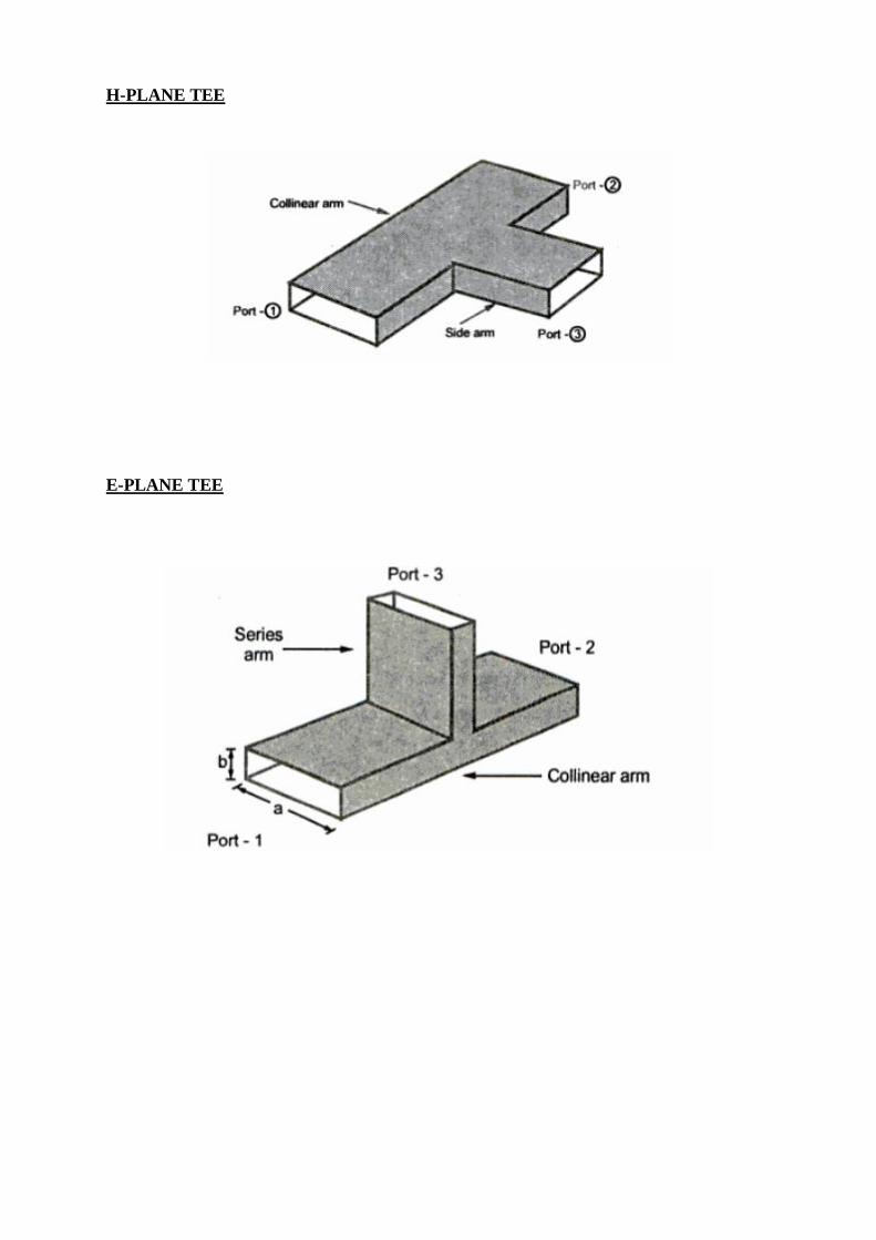
H-PLANE TEE
E-PLANE TEE

EXPT. NO. 1 STUDY OF MICROWAVE COMMUNICATION
DATE:
AIM:
To find the characteristics of given Magic Tee, E-plane and H-plane
COMPONENTS REQUIRED:
1. Micro wave source(klystron power supply)
2. Klystron Mount
3. Isolator
4. Variable Attenuator
5. Frequency meter
6. Magic – Tee
7. Power Detector
8. Matched termination ----- 2 No‘s
THEORY:
A T - junction is an intersection of three waveguides in the form of
English alphabet ‗T‘. There are several types of Tee Junctions.
TEE – JUNCTION:
In microwave circuits a wave guide line with three independent ports are
commonly referred to as Tee Junction.
Waveguide tees are three – port components. They are used to connect
branch (or) Section of the waveguide in series or parallel with the main
waveguide transmission Line for providing means of splitting and also of
combining power in a waveguide System.
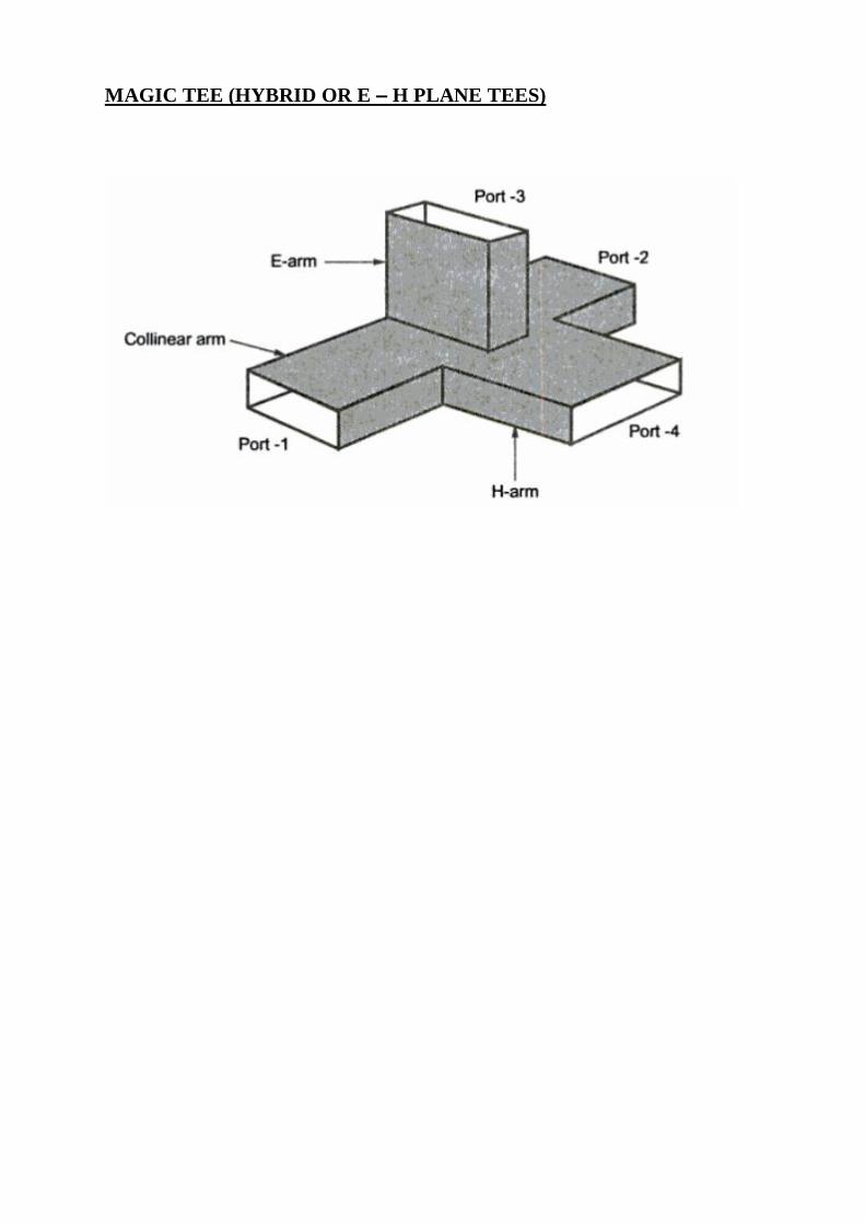
MAGIC TEE (HYBRID OR E – H PLANE TEES)

The basic types are
1. E – Plane Tee (series)
2. H - Plane Tee (shunt)
3. Magic Tees (Hybrid or E-H plane Tees).
E – PLANE TEE:
An E – plane tee is a waveguide tee in which the axis of its side arm is
parallel to the E – field of the main guide. A rectangular slot is cut along the
broader dimension of a Long waveguide and side arm is attached. Ports 1 and 2
are the collinear arms and port 3 is the E- arm.
When the waves are fed into the side arm (port 3), the waves appearing at
port 1 and Port 2 of the collinear arm will be in opposite phase and in the same
magnitude. If two input waves are fed into port 1 and port 2 of the collinear arm,
the output Wave at 3 will be opposite in phase and subtractive. Hence it is
called difference Arm
H – PLANE TEE:
An H –Plane Tee junction is formed by cutting a rectangular slot along
width of a main waveguide and attaching another waveguide, the side arm is
called the H-arm. Ports 1 and 2 are the collinear arms and port 3 is the H- arm.
If two input waves are fed into port 1 and port 2 of the collinear arm, the
output wave at port 3 will be in phase and additive. Because of this, the third
port is called the sum Arm. All three arms of H – Plane tee lie in the plane of
magnetic field, the magnetic field itself into the arms. This is also called as
current junction.
MAGIC TEES (HYBRID OR E – H PLANE TEES):
Here rectangular slots are cut both along the width and breadth of a long
waveguide and side arms are attached. Ports 1 and 2 are collinear arms, port 3 is
the H- arm, and port 4 is the E- arm. So Magic tee is the combinations of E and
H Plane Tee.
A wave incident at port 3 (E –arm) divides equally between ports 1 and 2
but opposite in phase with no coupling to port (H-ram).
A wave fed into collinear port 1 or 2 will not appear in the other collinear
port 2 or 1. Hence two collinear ports 1 and 2 are isolated from each other.


PROCEDURE:
1. Arrange the bench setup with out connecting magic – tee/E-plane/ H-Plane
and measure the input power.
2. Now connect the Tee junctions and note down the output power at port 2,
port 3 & port 4.
3. Substitute the value of the port currents to obtain the scattering parameters
of given magic – tee.
4. For various values of input power find the scattering matrix.
RESULT:
Thus the characteristics of given microwave devices characteristics was studied and
verified.
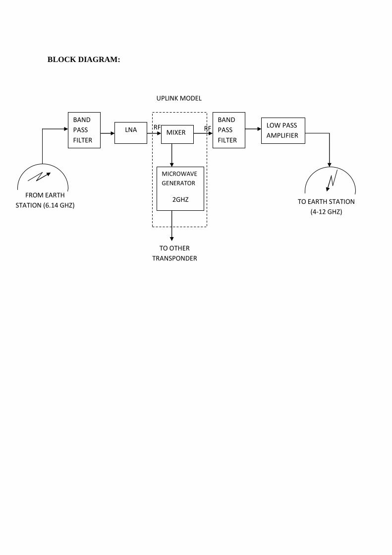
BLOCK DIAGRAM:
BAND
PASS
FILTER
LNA MIXER
BAND
PASS
FILTER
LOW PASS
AMPLIFIER
MICROWAVE
GENERATOR
2GHZ
TO OTHER
TRANSPONDER
FROM EARTH
STATION (6.14 GHZ) TO EARTH STATION
(4-12 GHZ)
UPLINK MODEL
RF RF
EXPT. No.:2 SIMULATION OF SATELLITE LINK BUDGET ANALYSIS
Date:
Aim
To Design and simulate the satellite link budget analysis.
Theory:
Uplink Model:
A satellite system has 3 basic reaction uplink, satellite transponder and downlink. The
primary component is earth station transmitter. A typically transmitter has IF modulator. A
typically transmitter IF-RF microwave up convertor and some band limiting the output
spectrum. If modulator converts input baseband to FN PSK/QAM intermediate frequency.
The up converter converts IF-RF the HPA provide adequate gain and output power to
propagate the signal to transponder. HPA‘s commonly used are krypton‘s and travelling wave
tubes.
Transponder:
It consists of input based limiting BPF, input LAN, frequency translators, LPA and output
BPF. It is a RF repeater. The input BPF limits the total noise applied to LAN (tuned diode).
The output of LNA is fed to frequency translator which converts high band uplink to low
band downlink frequency. The LPP amplifier RF signal for transmission through the
downlink to each earth station receiver.
Downlink Model:
An earth station receive includes, input BPF, LNA, RF-IF down converter. The LNA is
highly sensitive, Low noise device (Tunnel diode) parametric amplifier. The RF-IF down
converter is mixer that converts RF-IF frequency.
Satellite system parameter:
EIRP: Effective isotropic radiated power
It is defined as an equivalent transmits power.
EIRP=Pt*Gt
Where Pt=Antenna power input (w)
Gt= Transmitter antenna gain (unit less)
d=Distance between transmitter & receiver

SIMULATION OF SATELLITE LINK BUDGET ANALYSIS:
PROGRAM CODING:
#include<stdio.h>
#include<conio.h>
#include<math.h>
Void main()
{
float EIRP1, EIRP2, F_pathloss1, F_path loss2;
float G_Tel1,G-Tel2,Atm_loss1,Atm_loss2;
float C_N_up,C-N_down,C_N_overall;
clrscr();
printf(―\n Enter the uplink parameters:‖);
printf(―\n Enter the EIRP(dBw):‖);
scanf(―%f‖,& EIRP);
printf(―\n Enter the free space path loss (dB):‖);
scanf(―%f‖,&F_pathloss1);
printf(―\n Enter the G/Te ratio(dB/k):‖);
scanf(―%f‖,&G_Te1);
printf(―\n Enter the Atmospheric loss(dB):‖);
scanf(―%f‖,&Atm_loss1);
printf(―\n Enter the downlink parameters(dB):‖);
printf(―\n Enter the EIRP(dBw):‖);
scanf(―%f‖,& EIRP2);
printf(―\n Enter the free space path loss (dB):‖);
scanf(―%f‖,&F_pathloss2);
printf(―\n Enter the G/Te ratio(dB/k):‖);
scanf(―%f‖,&G_Te2);
printf(―\n Enter the Atmospheric loss(dB):‖);
scanf(―%f‖,&Atm_loss2);
C_N_up=EIRP_F-pathloss1+G-Te1-Atm_loss1+228.6;
C_N_down = EIRP2_F_pathloss2+G-Te2-Atm_loss2+228.6;
C_N_overall = ((1/C_N_up)+(1/C_N_down));
C_N_overall= 1/C_N_overall;
Printf(―C/N_uplink=%f‖,C_N_up);
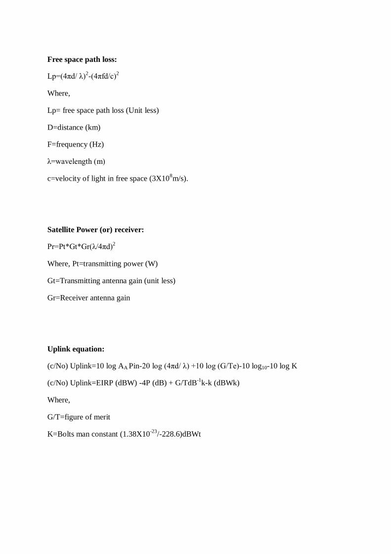
Free space path loss:
Lp=(4πd/ λ)2-(4πfd/c)
2
Where,
Lp= free space path loss (Unit less)
D=distance (km)
F=frequency (Hz)
λ=wavelength (m)
c=velocity of light in free space (3X10⁸m/s).
Satellite Power (or) receiver:
Pr=Pt*Gt*Gr(λ/4πd)2
Where, Pt=transmitting power (W)
Gt=Transmitting antenna gain (unit less)
Gr=Receiver antenna gain
Uplink equation:
(c/No) Uplink=10 log AA Pin-20 log (4πd/ λ) +10 log (G/Te)-10 log10-10 log K
(c/No) Uplink=EIRP (dBW) -4P (dB) + G/TdB-1
k-k (dBWk)
Where,
G/T=figure of merit
K=Bolts man constant (1.38X10⁻²³
/-228.6)dBWt

Printf(―C/N_downlink=%f‖,C_N_down);
Printf(―C/N_overall=%f‖,C_N_overall);
getch();
}
SAMPLE INPUT & OUTPUT:
Enter the uplink Parameter:
Enter the EIRP(dBw):90
Enter the free space path loss (dB):5.3
Enter the G/Te ratio (dB/k):206.5
Enter the atmospheric loss (dB):0.6
Enter the downlink parameter
Enter the EIRP(dBw):40.2
Enter the free space path loss (dB):205.6
Enter the G/Te ratio (dB/k):37.7
Enter the atmospheric loss (dB):4
C/N_uplink:579.799988
C/N_downlink:96.899994
C/N_overall:81.917374
The satellite link analysis is acceptable
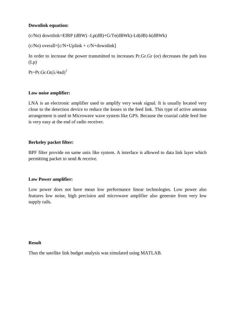
Downlink equation:
(c/No) downlink=EIRP (dBW) -Lp(dB)+G/Te(dBWk)-Ld(dB)-k(dBWk)
(c/No) overall=[c/N+Uplink + c/N+downlink]
In order to increase the power transmitted to increases Pr.Gr.Gr (or) decreases the path loss
(Lp)
Pt=Pr.Gr.Gt(λ/4πd)2
Low noise amplifier:
LNA is an electronic amplifier used to amplify very weak signal. It is usually located very
close to the detection device to reduce the losses in the feed link. This type of active antenna
arrangement is used in Microwave wave system like GPS. Because the coaxial cable feed line
is very easy at the end of radio receiver.
Berkeley packet filter:
BPF filter provide on same unix like system. A interface is allowed to data link layer which
permitting packet to send & receive.
Low Power amplifier:
Low power does not have mean low performance linear technologies. Low power also
features low noise, high precision and microwave amplifier also generate from very low
supply rails.
Result
Thus the satellite link budget analysis was simulated using MATLAB.

ALGORITHM:
IIR FILTER:
1. Start
2. Open a new .m file
3. Clear the screen
4. Get the value of alphap, alphas, omegap, omegas.
5. Compute the function for [n,wc], [nu,de],[nu1,de1] and [h,w] using the respective
function.
6. Display n,wc,nu,de,nu1,de1
7. Plot the graph for w versus abs(h)
8. Mark the title.
9. Mark the x-label and y-label
10. Stop
FIR FILTER:
1. Start
2. Open a new .m file.
3. Clear the screen and assume N as 25.
4. Compute the values for alphas, eps, wc, n, hd, wn, wr, hu ct and [h,w] using
respective formulae and function.
5. Compute wh using hanning (N) function
6. Compute hann using hann=hd*wh‘
7. Obtain the value of [hr,w] using frequency function
8. Plot the graph
9. Compute when using hamming (N) function
10. Compute hamm using hamm=hd*whm‘
11. Obtain the value of [h2,w] using frequency function
12. Plot the graph
13. Compute wb, using blackman (N) function
14. Compute a h black using hblack=hd*wb1
15. Obtain the value of [a3,w]using frequency function
16. Plot the graph
17. Mark the title
18. Give the X label and Y label
19. Mark the legend
20. Stop.
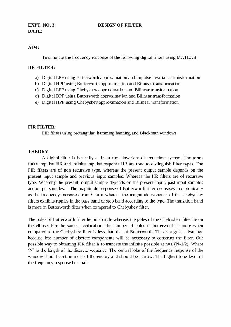
EXPT. NO. 3 DESIGN OF FILTER
DATE:
AIM:
To simulate the frequency response of the following digital filters using MATLAB.
IIR FILTER:
a) Digital LPF using Butterworth approximation and impulse invariance transformation
b) Digital HPF using Butterworth approximation and Bilinear transformation
c) Digital LPF using Chebyshev approximation and Bilinear transformation
d) Digital BPF using Butterworth approximation and Bilinear transformation
e) Digital HPF using Chebyshev approximation and Bilinear transformation
FIR FILTER:
FIR filters using rectangular, hamming hanning and Blackman windows.
THEORY:
A digital filter is basically a linear time invariant discrete time system. The terms
finite impulse FIR and infinite impulse response IIR are used to distinguish filter types. The
FIR filters are of non recursive type, whereas the present output sample depends on the
present input sample and previous input samples. Whereas the IIR filters are of recursive
type. Whereby the present, output sample depends on the present input, past input samples
and output samples. The magnitude response of Butterworth filter decreases monotonically
as the frequency increases from 0 to α whereas the magnitude response of the Chebyshev
filters exhibits ripples in the pass band or stop band according to the type. The transition band
is more in Butterworth filter when compared to Chebyshev filter.
The poles of Butterworth filter lie on a circle whereas the poles of the Chebyshev filter lie on
the ellipse. For the same specification, the number of poles in butterworth is more when
compared to the Chebyshev filter is less than that of Butterworth. This is a great advantage
because less number of discrete components will be necessary to construct the filter. Our
possible way to obtaining FIR filter is to truncate the infinite possible at n=± (N-1/2), Where
‗N‘ is the length of the discrete sequence. The central lobe of the frequency response of the
window should contain most of the energy and should be narrow. The highest lobe level of
the frequency response be small.
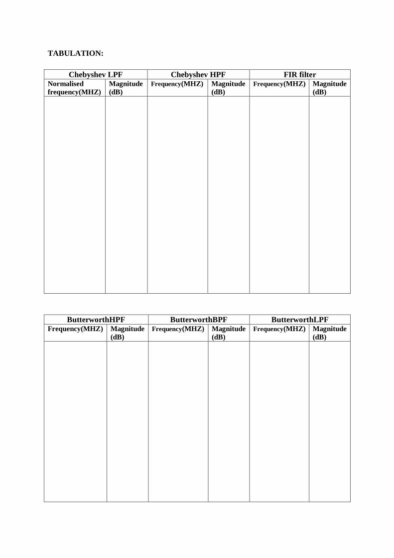
TABULATION:
Chebyshev LPF Chebyshev HPF FIR filter
Normalised
frequency(MHZ)
Magnitude
(dB)
Frequency(MHZ) Magnitude
(dB)
Frequency(MHZ) Magnitude
(dB)
ButterworthHPF ButterworthBPF ButterworthLPF
Frequency(MHZ) Magnitude
(dB)
Frequency(MHZ) Magnitude
(dB)
Frequency(MHZ) Magnitude
(dB)

FREQUENCY REPONSE OF CHEBYSHEV LPF USING BILINEAR TRANSFORMATION
clc;
alpap=2;
alphas=30;
omegap=0.5;
omegas=0.4;
[n,wc]=cheblord (omegap,omegas,alphap,alphas);
disp(n);
disp(wc);
[nu,de]=cheby1 (n,0.1,wc,‘s‘);
disp(nu);
disp(de);
[nu1,de1]=bilinear (nu, de, 1);
disp(nu1);
disp(de1);
[h,w]=freqz(nu1,de1);
plot(w,abs(h));
axis([0 3.5 0 2]);
title (‗frequency response of Chebyshev LPF using bilinear transformation‘);
xlabel (‗normalised frequency‘);
ylabel(‗magnitude(h(z)‘);
FREQUENCY REPONSE OF BUTTERWORTH LPF USING BILINEAR TRANSFORMATION
clc;
alpap=2;
alphas=30;
omegap=0.5;
omegas=0.4;
[n,wc]=buttord (omegap,omegas,alphap,alphas);
disp(n);
disp(wc);
[nu,de]=butter (n,0.1,wc,‘s‘);
disp(nu);
disp(de);
[nu1,de1]=impinvar (nu, de, 1);
disp(nu1);
disp(de1);
[h,w]=freqz(nu1,de1);
plot(w,abs(h));
axis([0 3.5 0 2]);
title (‗frequency response of Butterworth LPF using bilinear transformation‘);
xlabel (‗normalised frequency‘);
ylabel(‗magnitude(h(z)‘);

FREQUENCY REPONSE OF CHEBYSHEV HPF USING BILINEAR TRANSFORMATION
clc;
alpap=2;
alphas=70;
omegap=0.2;
omegas=0.4;
[N,wc]=cheblord (omegap,omegas,alphap,alphas);
disp(N);
disp(wc);
[Nu,De]=cheby1 (N,0.1,wc,‘high‘,‘s‘);
disp(Nu);
disp(De);
[Nu1,de1]=bilinear (Nu, De, 1);
disp(Nu1);
disp(De1);
[H,w]=freqz(Nu1,De1);
plot(w,abs(H));
axis([0 3.5 0 2]);
title (‗Frequency response of Chebyshev HPF using bilinear transformation‘);
xlabel (‗Normalised Frequency‘);
ylabel(‗Magnitude|H(z)|‘);
FREQUENCY REPONSE OF BUTTERWORTH HPF USING BILINEAR TRANSFORMATION
clc;
alpap=2;
alphas=30;
omegap=0.6;
omegas=0.2;
[n,wc]=buttord (omegap,omegas,alphap,alphas);
disp(n);
disp(wc);
[nu,de]=butter1 (n,wc,‘high‘,‘s‘);
disp(nu);
disp(de);
[nu1,de1]=bilinear (nu, de, 1);
disp(nu1);
disp(de1);
[h,w]=freqz(nu1,de1);
plot(w,abs(h));
axis([0 3.5 0 2]);
title (‗frequency response of Butterworth HPF using bilinear transformation‘);
xlabel (‗normalised frequency‘);
ylabel(‗magnitude(h(z)‘);

FREQUENCY REPONSE OF BUTTERWORTH BPF USING BILINEAR TRANSFORMATION
clc;
alpap=2;
alphas=30;
omegap=[0.2 0.8];
omegas=[0.4 0.6];
[n,wc]=buttord (omegap,omegas,alphap,alphas);
disp(n);
disp(wc);
[nu,de]=butter (n,wc,‘bandpass‘,‘s‘);
disp(nu);
disp(de);
[nu1,de1]=bilinear (nu, de, 1);
disp(nu1);
disp(de1);
[h,w]=freqz(nu1,de1);
plot(w,abs(h));
axis([0 3.5 0 2]);
title (‗frequency response of Butterworth BPF using bilinear transformation‘);
xlabel (‗normalised frequency‘);
ylabel(‗magnitude(h(z)‘);

FREQUENCY REPONSE OF LOW PASS FIR FILTERS FOR DIFFERENT WINDOWS
clear all;
clc;
hold on;
N=25;
alpha=(N-1)/2;
eps=0.001;
wc=3.14/2;
n=0:1:N-1;
hd=(sin ((n-alpha+eps)*3.14)-sin(wc*(n-alpha+eps)))/((n-alpha+eps)*3.14);
wn=0:0.001:3.14;
wr=boxcar(N);
hrect=hd.*wr‘;
[h,w]=freqz(hrect,1,wn);
plot(w/3.14,20*log(abs(h)),‘-k‘);
%HANNING WINDOW
wh=hanning (N);
hann=hd.*wh‘;
[h1,w]=freqz(hann,1,wn);
plot(w/3.14,20*log(abs(h1)),‘-k‘);
%HAMMING WINDOW
whm=hamming (N);
hamm=hd.*whm‘;
[h2,w]=freqz(hamm,1,wn);
plot(w/3.14,20*log(abs(h2)),‘--k‘);
%BLACKMAN WINDOW
wb1=blackman(N);
hblack=hd.*wb1‘;
[h3,w]=freqz(hblack,1,wn);
plot(w/3.14,20*log(abs(h3)),‘+k‘);
title(‗frequency response of low pass filters for different windows‘);
xlabel(‗NORMALISED FREQUENCY‘);
ylabel(‗MAGNITUDE |H(z)|‘);
disp(‗x,y‘);
legend(‗RECTANGULAR‘,‘HANNING‘,‘HAMMING‘,‘BLACKMAN‘);

Viva questions:
1. Define filter:
A filter is a reactive network that freely passes the desired bands of the frequency and
totally suppressing all other bands of frequencies.
2. Mention the types of filter:
Low pass filter, high pass filter, band pass filter and band stop filter
3. What is ideal filter?
An ideal filter offers zero attenuation in the pass band and infinite attenuation in stop
band.
Result:
Thus the frequency response of the digital filters was simulated using MATLAB.
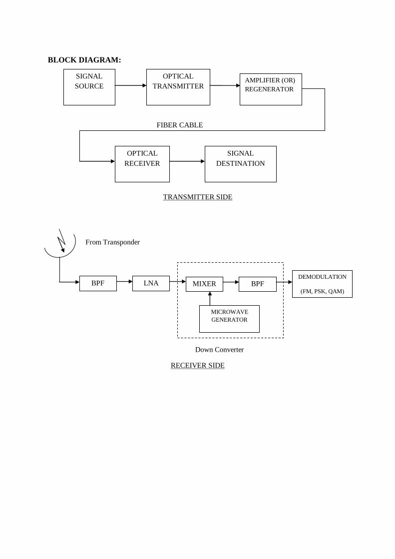
BLOCK DIAGRAM:
TRANSMITTER SIDE
RECEIVER SIDE
SIGNAL
SOURCE
OPTICAL
TRANSMITTER AMPLIFIER (OR)
REGENERATOR
OPTICAL
RECEIVER
SIGNAL
DESTINATION
FIBER CABLE
BPF LNA MIXER BPF DEMODULATION
(FM, PSK, QAM)
MICROWAVE
GENERATOR
From Transponder
Down Converter

EXPT. NO.4 SIMULATION OF FIBER OPTIC LINK POWER BUDGET ANALYSIS
Date:
Aim:
To design and simulate the fiber optic link power budget for the given link parameter
using MATLAB software.
Theory:
The 3 primary building blocks are Tr, Rr and optical fiber cable. The transmitter is
comprised of voltage current converter. Light source, source to fiber interface. The fiber
guide is transmission medium which is glass, plastic cable. The regenerator are used to
reconstruct the receiver include a fiber to interface detection and a current to voltage
convertor.The light source can be modulated by analog1 digital signal. The voltage current
converter serves as electrical interface between light source and circuitry. They are source of
LED or ILD. The light output of the source is proportional to magnitude of input voltage.
The source light coupler couple the light by light source into cable. The fiber light detector
coupling device is also a mechanical coupler. The light detectors are PIN and APD. A current
voltage controller transforms changes in detector current to change in voltages.
Link equation:
Pr=Pt-losses----------------(1)
(or)
Pt=Pt-Pr
Where
Pt=power transmitted (dBM)
Pr=power received (dBM)
Pt=Total power loss (dB)
Pt=2lc=α1+µs----------------(2)
Where, Pt=Total power loss(dB)
Lc=connector loss
L=length of cable
µs=external losses.
α=attenuator loss.

SIMULATION OF OPTIC FIBER LINK BUDGET ANALYSIS:
PROGRAM CODING:
#include<stdio.h>
#include<conio.h>
#include<math.h>
void main()
{
float con_loss, Att_loss, length, sys_mar, T_pow, R_Power,T_loss,Pt;
clrscr();
X;
printf(―\n Enter the losses:‖);
printf(―\n Enter the connector loss (dB):‖);
scanf(―%f‖,&Att_loss);
printf(―\n Enter the Attenuation loss (dB/km):‖);
scanf(―%f‖,&Att_loss);
printf(―\n Enter the length of the fiber(km):‖);
scanf(―%f‖,&length);
printf(―\n Enter the system margin(dB):‖);
scanf(―%f‖,&sys_mar);
printf(―\n Enter the power transmitted (dBW)‖)
scanf(―%f‖,&T_Pow);
printf(―\n Enter the received (dBW)‖)
scanf(―%f‖,&R_Pow);
T_loss=2*con_loss+Att_loss*length+sys_mar;
Pt=T_Pow-T_loss;
Printf(‗\n Total Power Loss=%f‘,T_loss);
Printf(―\n Transmitted Power=%f‖,Pt);


Printf(―\n Received Power=%f‖,R_Power);
if(Pt>=R_Power)
printf(―\n The optical fiber link analysis is acceptable‖):
else
goto X;
getch();
}
SAMPLE INPUT AND OUTPUT:
Enter the losses:
Enter the connector loss (dB):1
Enter the attenuation loss (dB/km):3
Enter the length of the fiber (km);5
Enter the system margin (dB):6
Enter the power transmitted (dBW):-69897
Enter the received power (dBM):23
Total Power loss (dB):23
Transmitted power—16.094379
Received power = -39.094379
The Optical fiber link analysis is acceptable
Optical source:
Solid state LED & ILD are primarily source for optical fiber transmission because their light
output can be rapidly controlled by varying their bias current.
Coupling loss must be considered for evolution of the source. Typically ILD‘s will launch in
18dB more power than the LED‘s are attractive for the use. Instead of ILD‘s because of
lower cost, longer life time and wide temperature range.
Optical Detector:
The optical receiver consists of an optical detector and amplifier that are provided for output
that reproduce the input signal.
The two types of solid state detector suited for moderate to high bit ratio. The optical fiber
receivers they are PIN layer. The diode and avalanche Photo diode together called as APD. It
requires more power and it is costly but it is more sensitive.
Power Margin:
Power margin ≥ 6dB (D0=10dB) for every link.
Dynamic ranges:
Dynamic range ≥ 20dB for Optical receiver.
Multimode graded index fiber:
A multimode graded index fiber has a core of radius (r). Unlike the step index fiber.
The value of m1 decreases as the distance (r) from the centre of fiber. The values of n1
decreases until it approach the value of refractive index of cladding n2. The value of n1 must
be higher than the value of n2.
Result:
Thus the fiber optic link budget analysis was simulated using MATLAB.
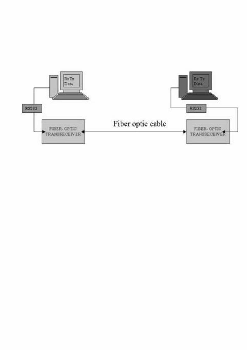
EXPT. NO.5 PC TO PC COMMUNICATION
Date:
Aim
To study the PC to PC communication by establishing an optical link.
Components Requirements:
1. Optical trainer kit
2. Personal computer
3. Optical fiber cable
4. RS-232 serial interface.
Theory:
Serial communication uses a transmitter to send one bit at a time, over a single
communication link line to the receiver. This method can be used, when the data rate is low
or when data need to transmit over a long distance. There is no need of extra hardware then a
cable to connect two PC‘s. Serial communication requires the following parameters.
a) Baud rate of transmitter
b) Number of data bits
c) Optical parity bits
d) Number of stop bits.
Baud rate is a measure of how fast data are moving between PC‘s. RS 232 uses only two
voltage state called ―MARK‖ and ―SPACE‖. A start bit signal the beginning of each other
characteristics frame. It is a transition from MARK to SPACE voltages.
If the instrument is transmitting each subsequent bit is 0.103ms. an optical or optimal parity
bit follows the data bit in the character. The transmission on any character frame handled by a
start bit means ‗SPACE‘ Voltage.
RS232:
It includes electrical signal character and mechanical characteristics. It mainly used
for serial communication between pc and printer, modem and other equipment.
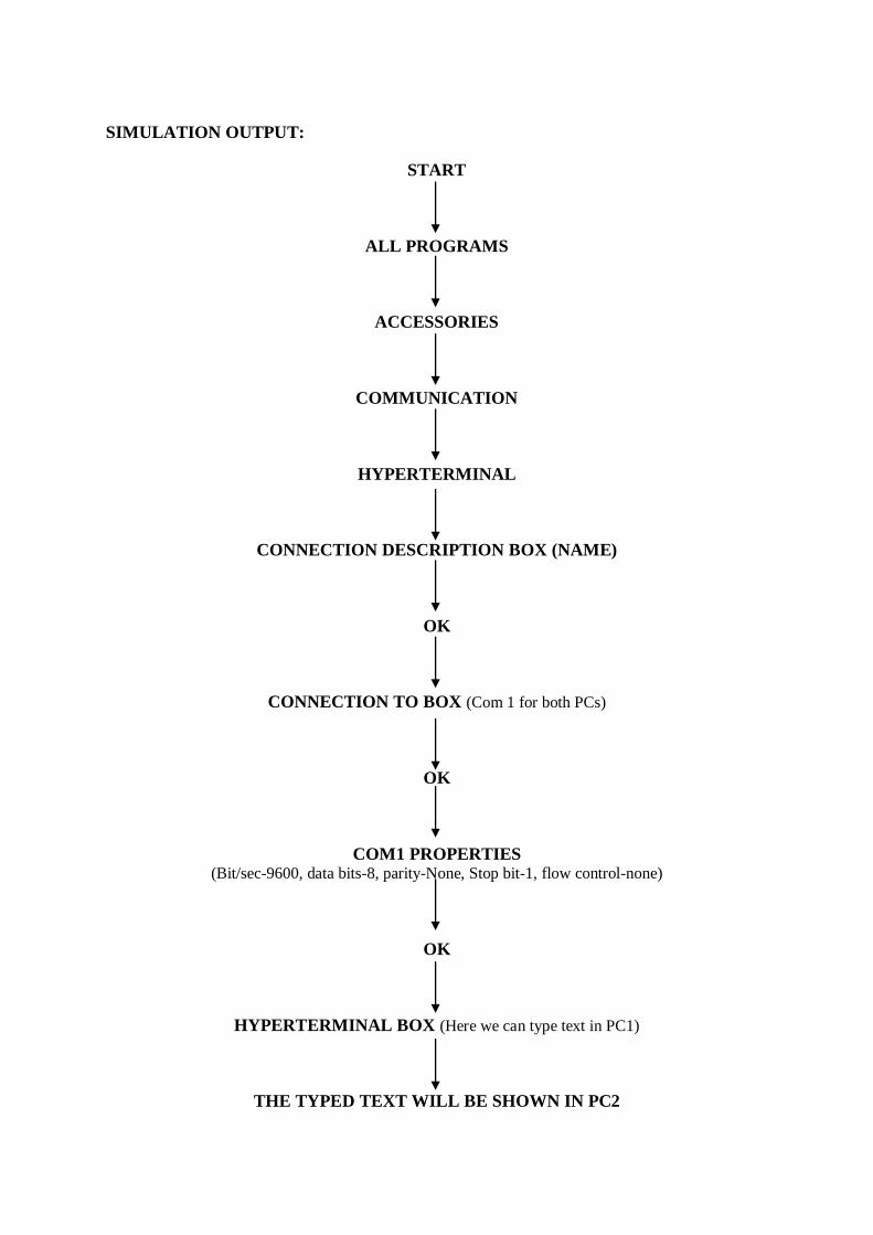
SIMULATION OUTPUT:
START
ALL PROGRAMS
ACCESSORIES
COMMUNICATION
HYPERTERMINAL
CONNECTION DESCRIPTION BOX (NAME)
OK
CONNECTION TO BOX (Com 1 for both PCs)
OK
COM1 PROPERTIES (Bit/sec-9600, data bits-8, parity-None, Stop bit-1, flow control-none)
OK
HYPERTERMINAL BOX (Here we can type text in PC1)
THE TYPED TEXT WILL BE SHOWN IN PC2

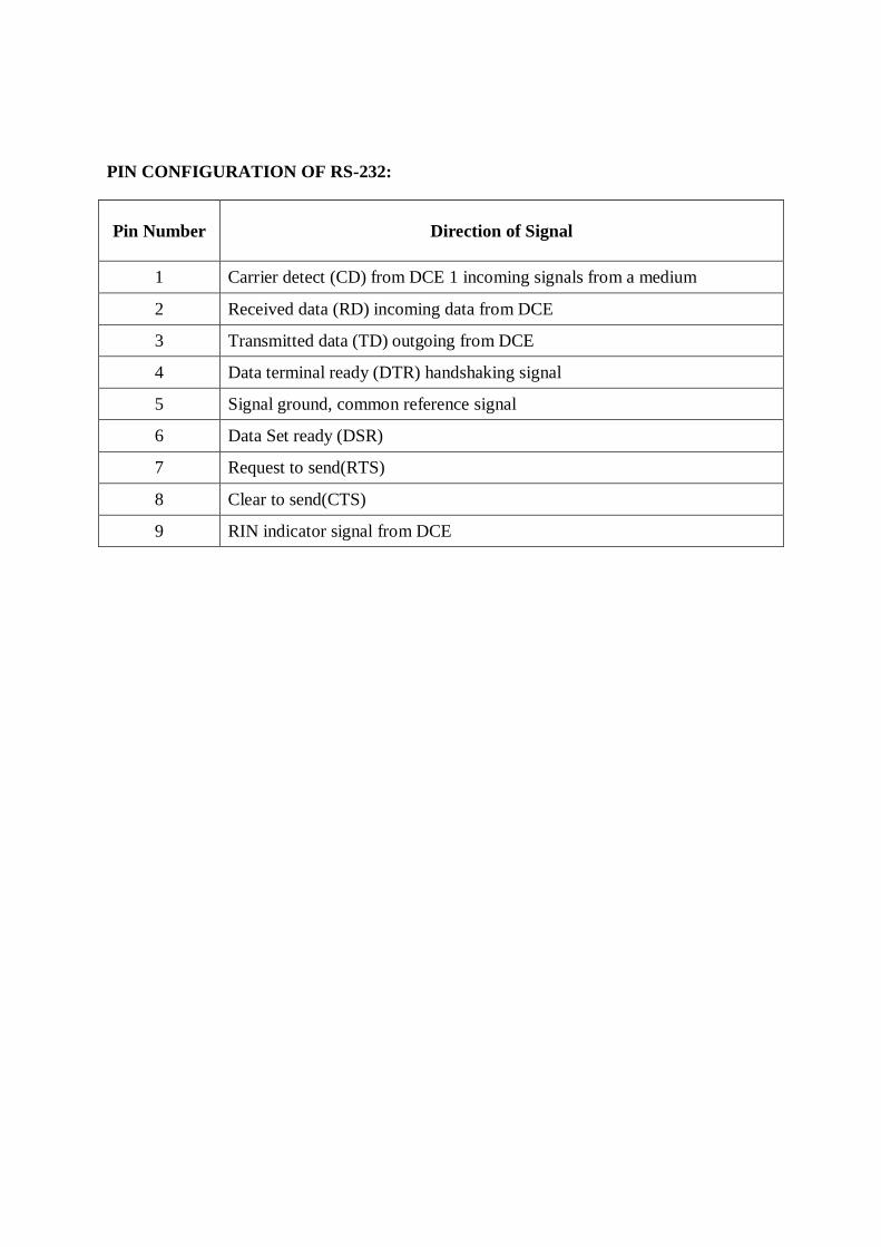
PIN CONFIGURATION OF RS-232:
Pin Number Direction of Signal
1 Carrier detect (CD) from DCE 1 incoming signals from a medium
2 Received data (RD) incoming data from DCE
3 Transmitted data (TD) outgoing from DCE
4 Data terminal ready (DTR) handshaking signal
5 Signal ground, common reference signal
6 Data Set ready (DSR)
7 Request to send(RTS)
8 Clear to send(CTS)
9 RIN indicator signal from DCE
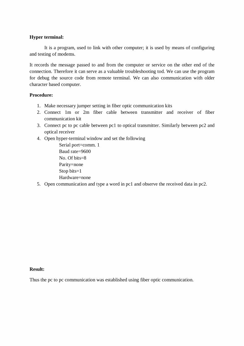
Hyper terminal:
It is a program, used to link with other computer; it is used by means of configuring
and testing of modems.
It records the message passed to and from the computer or service on the other end of the
connection. Therefore it can serve as a valuable troubleshooting tod. We can use the program
for debug the source code from remote terminal. We can also communication with older
character based computer.
Procedure:
1. Make necessary jumper setting in fiber optic communication kits
2. Connect 1m or 2m fiber cable between transmitter and receiver of fiber
communication kit
3. Connect pc to pc cable between pc1 to optical transmitter. Similarly between pc2 and
optical receiver
4. Open hyper-terminal window and set the following
Serial port=comm. 1
Baud rate=9600
No. Of bits=8
Parity=none
Stop bits=1
Hardware=none
5. Open communication and type a word in pc1 and observe the received data in pc2.
Result:
Thus the pc to pc communication was established using fiber optic communication.
SWEEP
SIGNAL
GENERATOR
POWER
DIVIDER
HARMONIC
FREQUENCY
CONVERTOR
AMPLITUDE
AND PHASE
METER
DEVICE
UNDER
TEST
LENGTH
EQUQLIZER
32.8 PF 32.8 PF
91.3nH
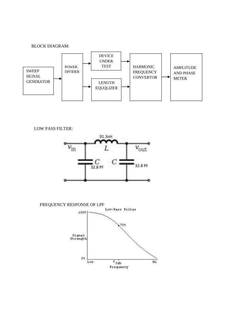
BLOCK DIAGRAM:
LOW PASS FILTER:
FREQUENCY RESPONSE OF LPF
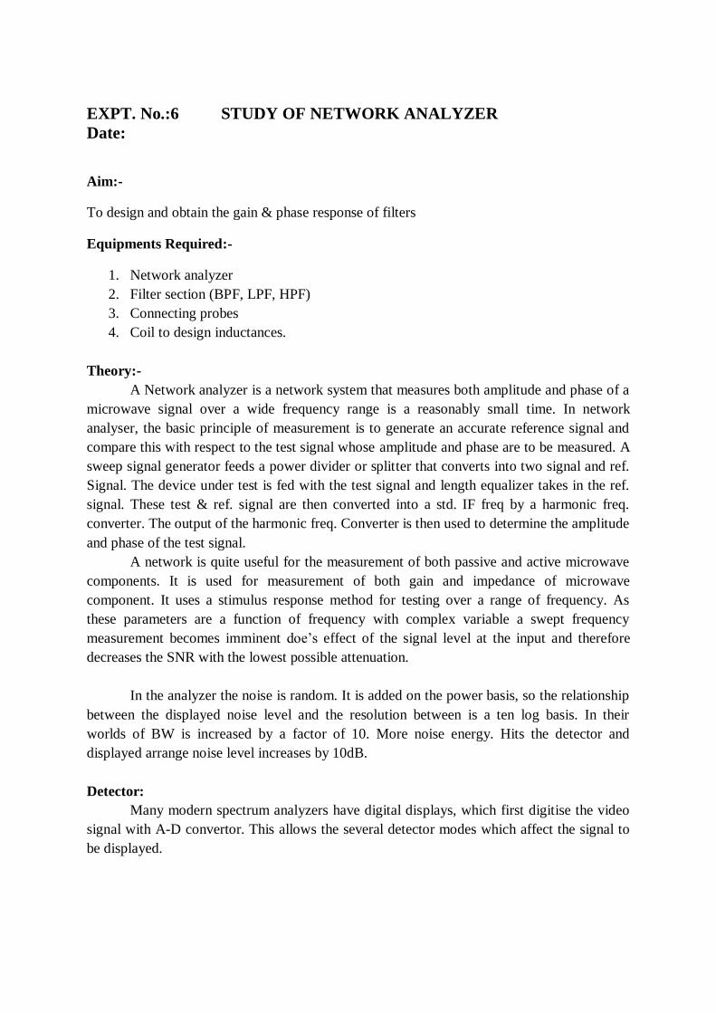
EXPT. No.:6 STUDY OF NETWORK ANALYZER
Date:
Aim:-
To design and obtain the gain & phase response of filters
Equipments Required:-
1. Network analyzer
2. Filter section (BPF, LPF, HPF)
3. Connecting probes
4. Coil to design inductances.
Theory:-
A Network analyzer is a network system that measures both amplitude and phase of a
microwave signal over a wide frequency range is a reasonably small time. In network
analyser, the basic principle of measurement is to generate an accurate reference signal and
compare this with respect to the test signal whose amplitude and phase are to be measured. A
sweep signal generator feeds a power divider or splitter that converts into two signal and ref.
Signal. The device under test is fed with the test signal and length equalizer takes in the ref.
signal. These test & ref. signal are then converted into a std. IF freq by a harmonic freq.
converter. The output of the harmonic freq. Converter is then used to determine the amplitude
and phase of the test signal.
A network is quite useful for the measurement of both passive and active microwave
components. It is used for measurement of both gain and impedance of microwave
component. It uses a stimulus response method for testing over a range of frequency. As
these parameters are a function of frequency with complex variable a swept frequency
measurement becomes imminent doe‘s effect of the signal level at the input and therefore
decreases the SNR with the lowest possible attenuation.
In the analyzer the noise is random. It is added on the power basis, so the relationship
between the displayed noise level and the resolution between is a ten log basis. In their
worlds of BW is increased by a factor of 10. More noise energy. Hits the detector and
displayed arrange noise level increases by 10dB.
Detector:
Many modern spectrum analyzers have digital displays, which first digitise the video
signal with A-D convertor. This allows the several detector modes which affect the signal to
be displayed.
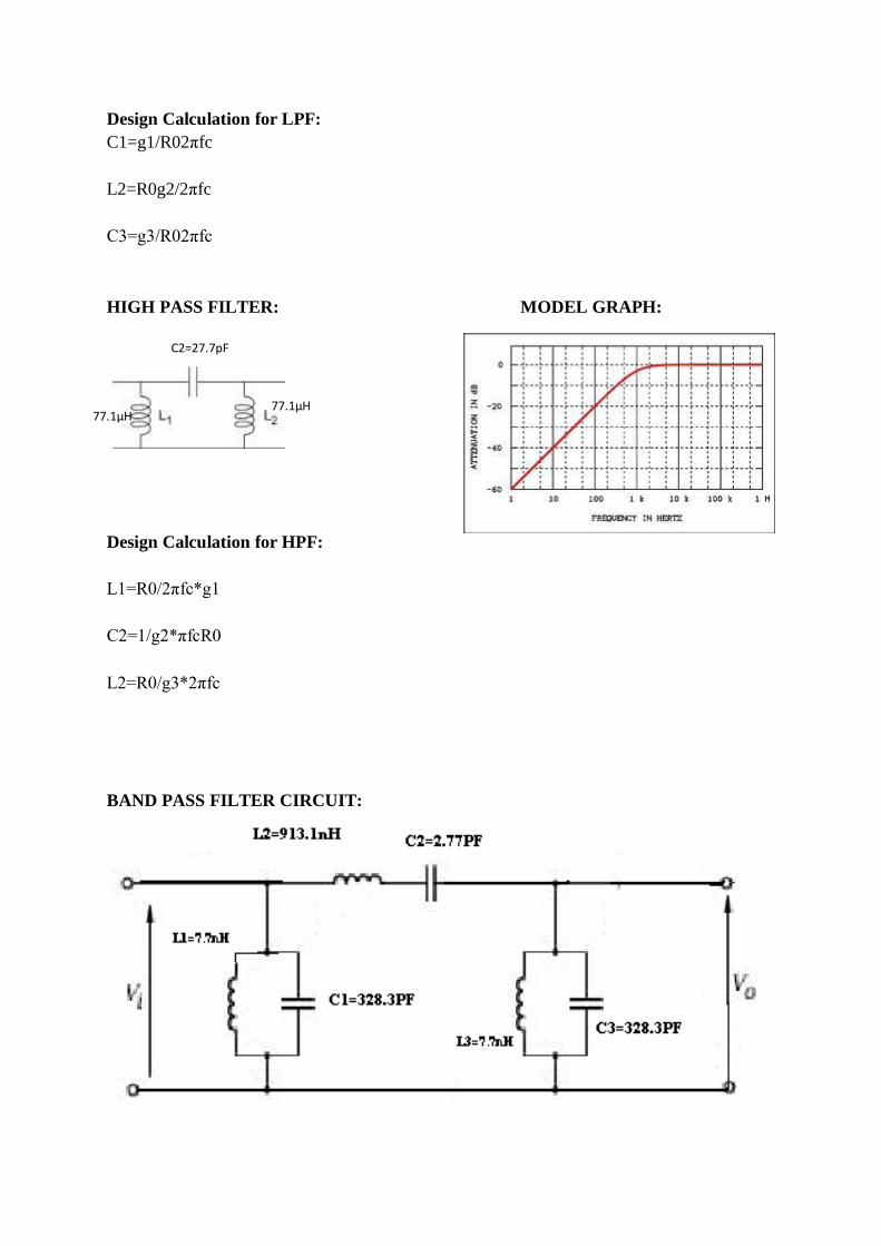
Design Calculation for LPF:
C1=g1/R02πfc
L2=R0g2/2πfc
C3=g3/R02πfc
HIGH PASS FILTER: MODEL GRAPH:
Design Calculation for HPF:
L1=R0/2πfc*g1
C2=1/g2*πfcR0
L2=R0/g3*2πfc
BAND PASS FILTER CIRCUIT:
77.1μH 77.1μH
C2=27.7pF
Video Filter:
It is a LPF located after the envelope detector and before the ADC. This filter
determines the BW of the video amplifier and also used to average or smoothen the trace seen
on the screen.
Network analyser:
It can be a scalar or vector. A scalar network analyzer provides only magnitude
characteristics of microwave device as a function of frequency. A vector network analyzer
can measure complex reflection (or) transmission characteristics of microwave devices. The
principle of measurement of both methods are same in that they compare the incident (or)
input power with the transmitted or reflected waves depending on the parameter to be
measured.
A vector network analyser can measure complex transmission reflection characteristics of
microwave devices as a function of frequency. In a scalar network analyser, a diode detector
is used, whereas in vector analyzer is a multi channel receiver used.
Filters:
Low pass prototype is the base for all types of filter such as HPF, BPF, and BSF scaling
information are used to design any filter from prototype. It can be scaled at any
characteristics impedance and cut off frequency.
Procedure:
1. Switch on the trainer and ensure the display ―TEST MENU‖
2. Select the filter test and press the ENTER key
3. Enter the values of start frequency and end frequency of filter (user select the start and
end frequency by using up, down, left, right key).
4. After selecting the desired frequency press ENTER key
5. For calculation purpose, connect the RF Out and DET in by using the probe.
6. After completion of calculation, press ENTER and remove the short & connect the filter
(LPF, HPF, BPF) between RF out and DET in.
7. After finishing the scanning process filter characteristics will be displayed.
8. Same procedure repeated for RF amplifier.
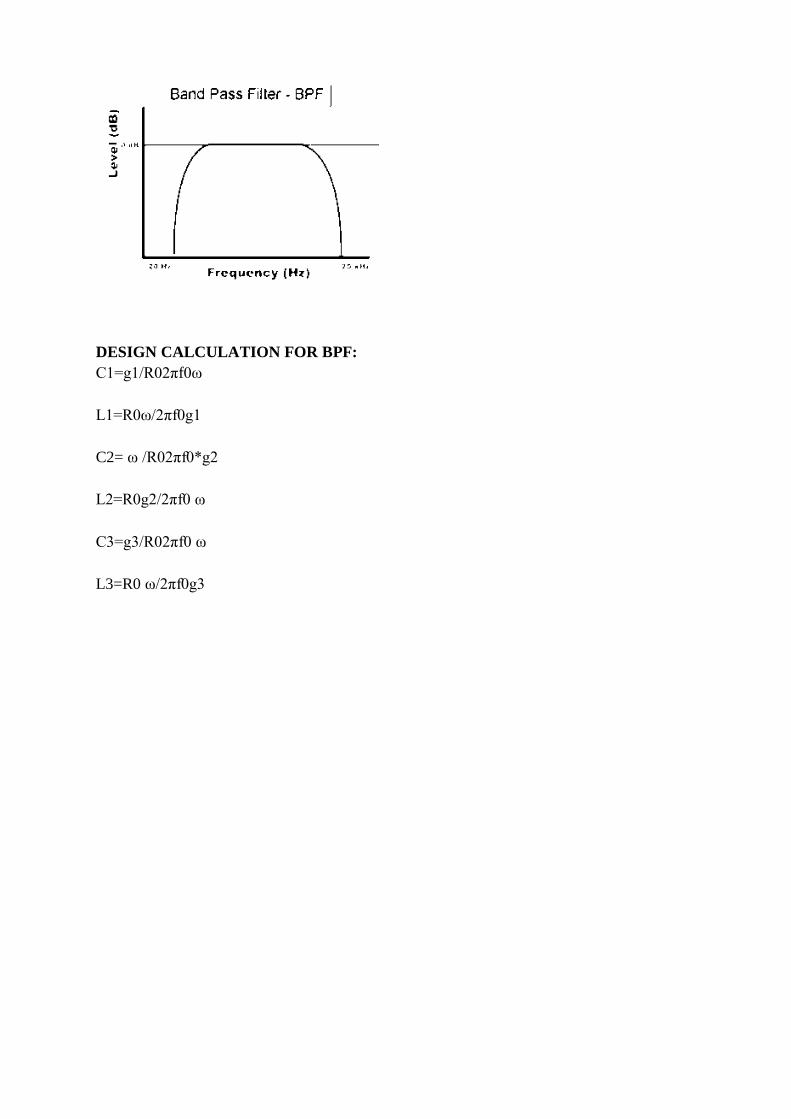
DESIGN CALCULATION FOR BPF:
C1=g1/R02πf0ω
L1=R0ω/2πf0g1
C2= ω /R02πf0*g2
L2=R0g2/2πf0 ω
C3=g3/R02πf0 ω
L3=R0 ω/2πf0g3


TABULATION:
Butterworth LPF Butterworth HPF Butterworth BPF
Normalised
frequency(MHZ)
Magnitude
(dB)
Normalised
frequency(MHZ)
Magnitude
(dB)
Normalised
frequency(MHZ)
Magnitude
(dB)

Result:
Thus the gain response and phase response of filters were determined by using network
analyser.
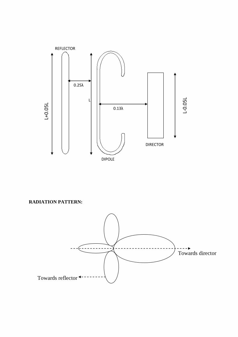
RADIATION PATTERN:
REFLECTOR L+
0.0
5L
0.25λ
DIPOLE
0.13λ
L-0
.05
L
DIRECTOR
L
Towards director
Towards reflector
EXPT. NO.7 DESIGN AND ANALYSIS OF TV SIGNAL USING SPECTRUM
ANALYZER
DATE:
AIM
To conduct and test the characteristics of yagi uda antenna for a given a given frequency
band.
COMPONENTS REQUIRED:
1. Spectrum analyzer
2. Twin cable
3. BNC cable
FORMULA
1. Centre frequency, fc=fs+fe/2
2. Length of dipole,λ=c/f, L=λ/2
3. Length of reflector, L+0.05L
4. Length of director,L-0.05L
5. Spacing between dipole and reflector=0.25λ
6. Spacing between dipole and director=0.13λ
THEORY:
Yagi uda antenna:
It is a high gain antenna and it is known after the professor S.Uda and H.Yagi who
invented it. It consists of a driven element reflector and one or more directors. The yagi uda
antenna is an array of driven element and called as active element where the power is fed
from the transistor. It is resonant half wave dipole and reflector and directors are called as
parasitic element. The parasitic element receives their excitation from the voltages induced in
them by current flow in the driven elements.
Reflector length =500/f (MHz)
Driven element length=475/ (MHz)
Director length = 455/f (MHz)
Spacing=0.1λ to 0.15λ
The parasitic element is clamped on a metallic support rod. The use of parasitic element in
conjunction with driven elements causes the dipole impedance to fall below 43Ω. It may be
also low as 25Ω. If these 3 elements are alone used, then such type of yagi uda antenna is
generally referred as beam antenna.
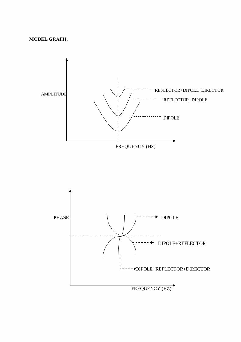
MODEL GRAPH:
FREQUENCY (HZ)
PHASE DIPOLE
DIPOLE+REFLECTOR
DIPOLE+REFLECTOR+DIRECTOR
FREQUENCY (HZ)
REFLECTOR+DIPOLE+DIRECTOR
REFLECTOR+DIPOLE
DIPOLE
AMPLITUDE

DESIGN CALCULATION:

TABULATION:
DIPOLE DIPOLE+REFLECTOR DIPOLE+REFLECTOR+DIRECTOR
Frequency
(MHZ)
Magnitude
(dB)
Frequency
(GHZ)
Magnitude
(dB)
Frequency
(GHZ)
Magnitude
(dB)

CHARACTERISTICS:
1. If three elements array is used then the antenna is called as beam antenna
2. It has unidirectional beam of moderate directivity with light weight, low cost and
simplicity in design.
3. With spacing of 0.1λ to 0.15λ a frequency bandwidth of the order of 12% obtained.
4. It provides a gain of order of 3dB
5. It also known as super directive due to its high gain or bandwidth per unit area of an
array.
6. Greater directivity is desired, more number of elements can be added for better TV
reception,
7. Fixed frequency device.
PROCEDURE:
1. The folded dipole length was made with respect to centre frequency ‗fc‘
2. The folded dipole was connected to the spectrum analyzer and the frequency pattern
was inferred.
3. The ‗fc‘ and the given values are checked and frequency curve was measured.
4. The ‗fc‘ was inferred for reflector and director.
5. The impedance of the folded dipole also noted.
RESULT:
Thus the design of yagi uda antenna for the given channel band was constructed and
the performance of antenna was determined using spectrum analyzer.
fc=_________GHz
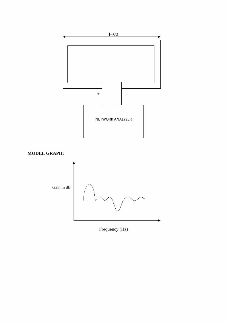
l=λ/2
+ -
MODEL GRAPH:
Frequency (Hz)
NETWORK ANALYZER
Gain in dB
EXPT. No.8 DESIGN OF FOLDED DIPOLE USING NETWORK ANALYZER
DATE:
AIM:
To design the folded dipole and check its frequency using network analyzer
REQUIREMENTS:
1. Folded dipole
2. Network analyzer
3. BNC cables
THEORY:
A folded dipole is made by 2 half wave dipole sections. One is continuous and
another split at the centre, folded dipoles mainly used for impedance matching. The radiation
pattern of folded dipole is same as the conventional half wave dipole. But the impedance
input of the forms is higher. A folded dipole differ from other dipoles by their directivity and
broadness in bandwidth, the directivity of the folded dipole is bidirectional because of the
distribution of the current in the parts of the folded dipole, input becomes higher as the ratio
of the two conductors are equal in magnitude and phase. The input terminals equal to the
square of the number of conductors comprising the antenna times the impedance at the
terminal of the conventional dipole.
The folded dipole is connected to the network analyzer to find the frequency
characteristics of the devices. The network analyzer graphically displays the gain VS
frequency characteristics and return loss. The sensitivity and wider range make the network
analyzer useful for communicating and measuring low level modulation.
TABULATION: For distance 8cm:
Return Loss (dB) VSWR (dB)
CALCULATION:


TABULATION: For distance 15cm:
Return Loss (dB) VSWR (dB)
CALCULATION:

PROCEDURE:
1. Switch on the network analyzer and select the mode of operation (option3)
2. Set the start frequency and stop frequency
3. Then fix the network analyzer for the internal calibration
4. Connect the micro strip in between network analyzer using BNC cable
5. The graphical representation of return loss and SWR shown in network analyzer
6. By changing the wavelength of dipole antenna we can measure the return loss for
different cut off frequency.
RESULT:
Thus the design of the folded dipole and its frequency characteristics analysis was
done by using network analyzer.
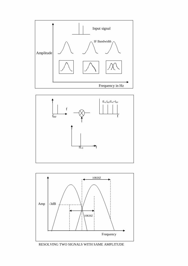
Input signal
Amplitude
Frequency in Hz
fL0 fRFfL0+fRF
f
fRF f
fL0 f
IF Bandwidth
-3dB
10KHZ
10KHZ
Frequency
Amp
RESOLVING TWO SIGNALS WITH SAME AMPLITUDE
EXPT. NO.9 SPECTRUM ANALYSIS OF MODULATED SIGNAL USING SPECTRUM
ANALYZER
DATE:
AIM:
To study the spectrum of communication circuits like AM, FM and FSK by using
spectrum analyzer.
EQUIPMENTS REQUIRED:
1. Spectrum Analyzer
2. Arbitrary waveform generator
3. 20 MHz dual oscilloscope
4. Multi meter
5. Connecting wires
THEORY:
The main components of spectrum analyzer are an RF input attenuator, input amplifier,
mixer, IF amplifier, IF filter, Envelope detector, video filter, CRT display, ramp generator.
Input section:
The input to the spectrum analyzer has a step attenuation followed by an amplifier.
The purpose of this input section is to control the signal level applied to the rest of the
instrument. If the signal level is too large, the analyzer circuit will saturate the mixer and
distort the signal, causing distorted products to appear along with the desired signal.
If the signal level is too small, it may be mashed by the noise present in the analyzer. Either
problem tends to reduce the dynamic range of the measurements. the new instruments
provide an auto range feature which automatically selects an appropriate input attenuation.
The input analyzer circuit is very sensitive and will not withstand much abuse. Careful
attention should be paid to the allowable signal level at the input particularly for microwave
analyzer.
Some instruments analyzer tolerate DC voltages at their inputs, but other require that no DC
be applied or be restricted to small amounts. The front end of the spectrum analyzer is made
with wide open, on the basis that we have no idea how many signals are involved in our
measurement in order to control somehow on the measured spectrum. It is necessary to add
LPF for image rejection.
A mixer is a device that converts a signal from one frequency to another. It is therefore,
sometimes called a frequency convertor device. The output of the two original signal consist
of f{L0} and f{RF} as well as the sum of these two signals IF filter and selectively.
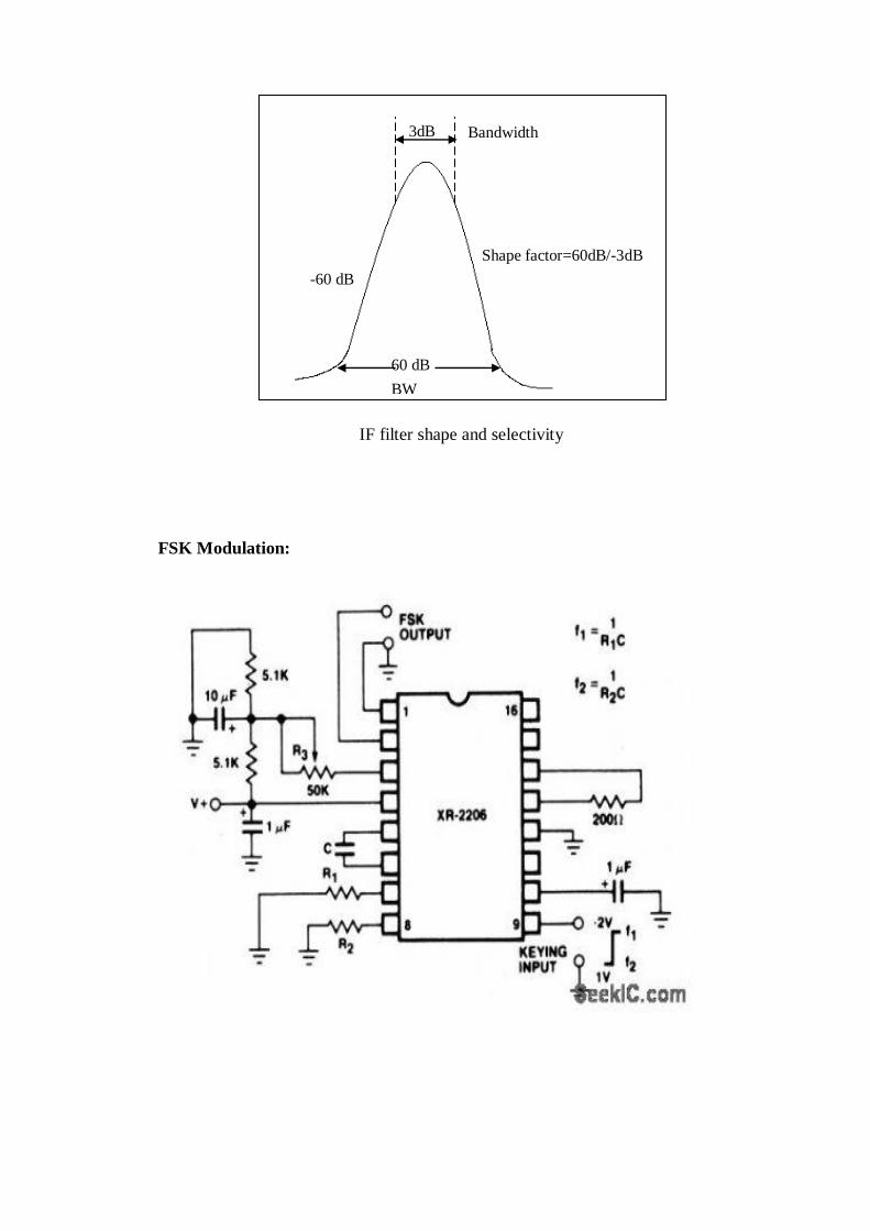
IF filter shape and selectivity
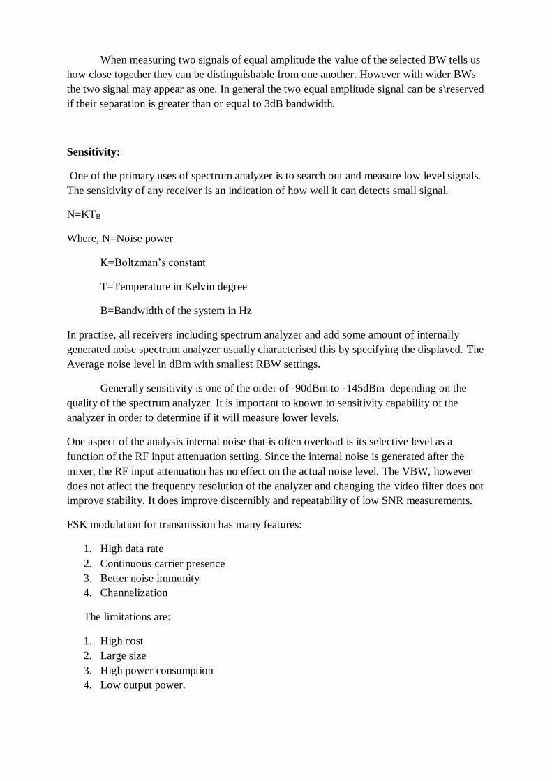
FSK Modulation:
Bandwidth 3dB
-60 dB
Shape factor=60dB/-3dB
60 dB
BW
When measuring two signals of equal amplitude the value of the selected BW tells us
how close together they can be distinguishable from one another. However with wider BWs
the two signal may appear as one. In general the two equal amplitude signal can be s\reserved
if their separation is greater than or equal to 3dB bandwidth.
Sensitivity:
One of the primary uses of spectrum analyzer is to search out and measure low level signals.
The sensitivity of any receiver is an indication of how well it can detects small signal.
N=KTB
Where, N=Noise power
K=Boltzman‘s constant
T=Temperature in Kelvin degree
B=Bandwidth of the system in Hz
In practise, all receivers including spectrum analyzer and add some amount of internally
generated noise spectrum analyzer usually characterised this by specifying the displayed. The
Average noise level in dBm with smallest RBW settings.
Generally sensitivity is one of the order of -90dBm to -145dBm depending on the
quality of the spectrum analyzer. It is important to known to sensitivity capability of the
analyzer in order to determine if it will measure lower levels.
One aspect of the analysis internal noise that is often overload is its selective level as a
function of the RF input attenuation setting. Since the internal noise is generated after the
mixer, the RF input attenuation has no effect on the actual noise level. The VBW, however
does not affect the frequency resolution of the analyzer and changing the video filter does not
improve stability. It does improve discernibly and repeatability of low SNR measurements.
FSK modulation for transmission has many features:
1. High data rate
2. Continuous carrier presence
3. Better noise immunity
4. Channelization
The limitations are:
1. High cost
2. Large size
3. High power consumption
4. Low output power.
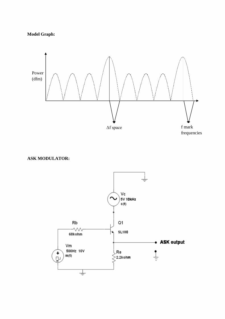
Model Graph:
ASK MODULATOR:
Δf space f mark
frequencies
Power
(dfm)

PROCEDURE:
1. Select the type of modulation for frequency shift keying
2. Set the carrier frequency which can range up to 20 MHz the carrier is a sine wave.
3. Set the hop frequency which is modulating signal a square wave range is limited.
4. Set the FSK rate which would mark the mark frequency and space frequency. It is
limited to 100 KHz.
5. The output performance in frequency domain can be viewed in spectrum analyzer.

TABULATION:
FREQUENCY (MHZ) GAIN IN dB

RESULT:
Thus the modulated signal was analyzed using spectrum analyzer.
fc=_________GHZ
EXPT NO. 10 STUDY OF RADAR TRAINER KIT
DATE:
AIM:
To study the RADAR trainer kit and study its working principle
THEORY:
RADAR is a system that uses electromagnetic waves to identify the range, altitude, direction
speed of both moving and fixed objects such as air crafts, ships, motor vehicle weather
information and terrain.
RADAR system has a transmitter that emits either microwave or radio waves that are
reflected by the largest and detected by a receiver, typically in the same location as the
transmitter.
PRINCIPLE OF RADAR:
Electromagnetic waves reflect from any large charge in the dielectric radar, absorbing
material containing resistive and some bodies magnetic substances is used on military vehicle
to reduces radar reflection.
Radar waves scatter in a variety of ways depending on the size of the radio wave and shape of
the target. Short radio waves reflect from curves and corners in a way similar to glut from a
rounded piece of glass. The most reflective targets for short wavelength have 900 angles
between reflective surfaces.
CONFIGURATIONS OF RADAR:
1. BISTATIC RADAR :
Bistatic radar in the r\name given to a radar system which comprises a transmitter and
receiver which are separated by a distance that is comparable to the expected target
distance.
2. CONTINUOS WAVE RADAR:
Continuous wave radar is system where known stable frequency continuous wave radio
energy is transmitted and received from any reflective objects.
3. DOPPLER RADAR:
Radar using the Doppler effect of the returned echoes from targets to measure their radial
velocity. It is used in air defence control, surrounding satellite etc

RADAR EQUATION:
The amount of power, a returning to the receiving antenna is given by the radar equation
Pr=Pt Gt Ar σFH/(4π)
2 Rt
2 Rr
2
Pt-transmitter power
Pr-Received Power
F-Pattern propagation
Rt-distance from the transmitter to the target
Rr-Distance from the target to the receiver.
4. FM-CW RADAR:
It is a radar system where known stable frequency continuous wave radio energy is
modulated by a triangular modulation signals so that is varies gradually and then mixes
with the signal reflected from a target object transmitter.
5. PLANAR ARRAY RADAR:
The planar array radar is a type of radar that uses a high planar array antenna a fixed
delay is established between horizontal arrays in the elevation plane.
6. PULSE DOPPLER RADAR:
It is a radar system capable of not only detecting target location. But also measuring its
radial velocity
DOPPLER EFFECT:
The Doppler Effect named after Austrian, physicist Christian Doppler who proposed
in 1842 is the change in frequency and wavelength of a wave for an observer moving
relative to the source of the waves. It is commonly used relative to the source of the
waves. It is commonly used when a vehicle surrounding a siren approaches passes and
needs from an observer.
F= [(V+Vr)/ (V+Vs)] F0
Where V-Velocity of waves in the medium
Vs-velocity of the source relative to the medium
Vr- velocity of the receiver relative to the medium
APPLICATION OF THE DOPPLER EFFECT:
1. Astronomy
2. Temperature
3. Radar
4. Medical imaging and blood flow measurement
5. Flow measurement
6. Velocity profile measurement.
Result:
Thus the radar trainer kit and its working principle were studied.