advanced communication lab 10ecl67 b.e - vi semester lab
TRANSCRIPT
QMP 7.1 D/F
Channabasaveshwara Institute of Technology
(An ISO 9001:2008 Certified Institution)
NH 206 (B.H. Road), Gubbi, Tumkur – 572 216. Karnataka.
Department of Electronics & Communication Engineering
Advanced Communication Lab
10ECL67
B.E - VI Semester
Lab Manual 2015-16
Name : _____________________________________
USN : _____________________________________
Batch : __________________ Section : ___________
Channabasaveshwara Institute of Technology
(An ISO 9001:2008 Certified Institution)
NH 206 (B.H. Road), Gubbi, Tumkur – 572 216. Karnataka.
Department of Electronics and Communication Engineering
Advanced Communication Lab
Version 1.0
February 2016
Prepared by: Reviewed by:
Pradeep N R Nagaraja P
Vidyarani K R Associate Professor
Harish S
Tejaswini S
Yashaswini T
Approved by:
Prof. Rajendra
Professor & Head,
Dept. of ECE
Channabasaveshwara Institute of Technology (An ISO 9001:2008 Certified Institution)
NH 206 (B.H. Road), Gubbi, Tumkur – 572 216. Karnataka.
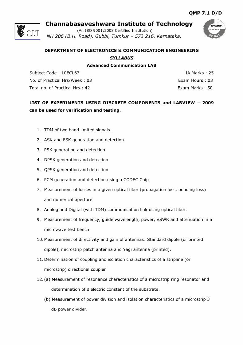
DEPARTMENT OF ELECTRONICS & COMMUNICATION ENGINEERING
SYLLABUS
Advanced Communication LAB
Subject Code : 10ECL67 IA Marks : 25
No. of Practical Hrs/Week : 03 Exam Hours : 03
Total no. of Practical Hrs.: 42 Exam Marks : 50
LIST OF EXPERIMENTS USING DISCRETE COMPONENTS and LABVIEW – 2009
can be used for verification and testing.
1. TDM of two band limited signals.
2. ASK and FSK generation and detection
3. PSK generation and detection
4. DPSK generation and detection
5. QPSK generation and detection
6. PCM generation and detection using a CODEC Chip
7. Measurement of losses in a given optical fiber (propagation loss, bending loss)
and numerical aperture
8. Analog and Digital (with TDM) communication link using optical fiber.
9. Measurement of frequency, guide wavelength, power, VSWR and attenuation in a
microwave test bench
10. Measurement of directivity and gain of antennas: Standard dipole (or printed
dipole), microstrip patch antenna and Yagi antenna (printed).
11. Determination of coupling and isolation characteristics of a stripline (or
microstrip) directional coupler
12. (a) Measurement of resonance characteristics of a microstrip ring resonator and
determination of dielectric constant of the substrate.
(b) Measurement of power division and isolation characteristics of a microstrip 3
dB power divider.
QMP 7.1 D/D
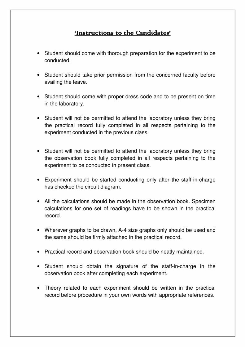
‘Instructions to the Candidates’‘Instructions to the Candidates’‘Instructions to the Candidates’‘Instructions to the Candidates’
• Student should come with thorough preparation for the experiment to be
conducted.
• Student should take prior permission from the concerned faculty before
availing the leave.
• Student should come with proper dress code and to be present on time
in the laboratory.
• Student will not be permitted to attend the laboratory unless they bring
the practical record fully completed in all respects pertaining to the
experiment conducted in the previous class.
• Student will not be permitted to attend the laboratory unless they bring
the observation book fully completed in all respects pertaining to the
experiment to be conducted in present class.
• Experiment should be started conducting only after the staff-in-charge
has checked the circuit diagram.
• All the calculations should be made in the observation book. Specimen
calculations for one set of readings have to be shown in the practical
record.
• Wherever graphs to be drawn, A-4 size graphs only should be used and
the same should be firmly attached in the practical record.
• Practical record and observation book should be neatly maintained.
• Student should obtain the signature of the staff-in-charge in the
observation book after completing each experiment.
• Theory related to each experiment should be written in the practical
record before procedure in your own words with appropriate references.
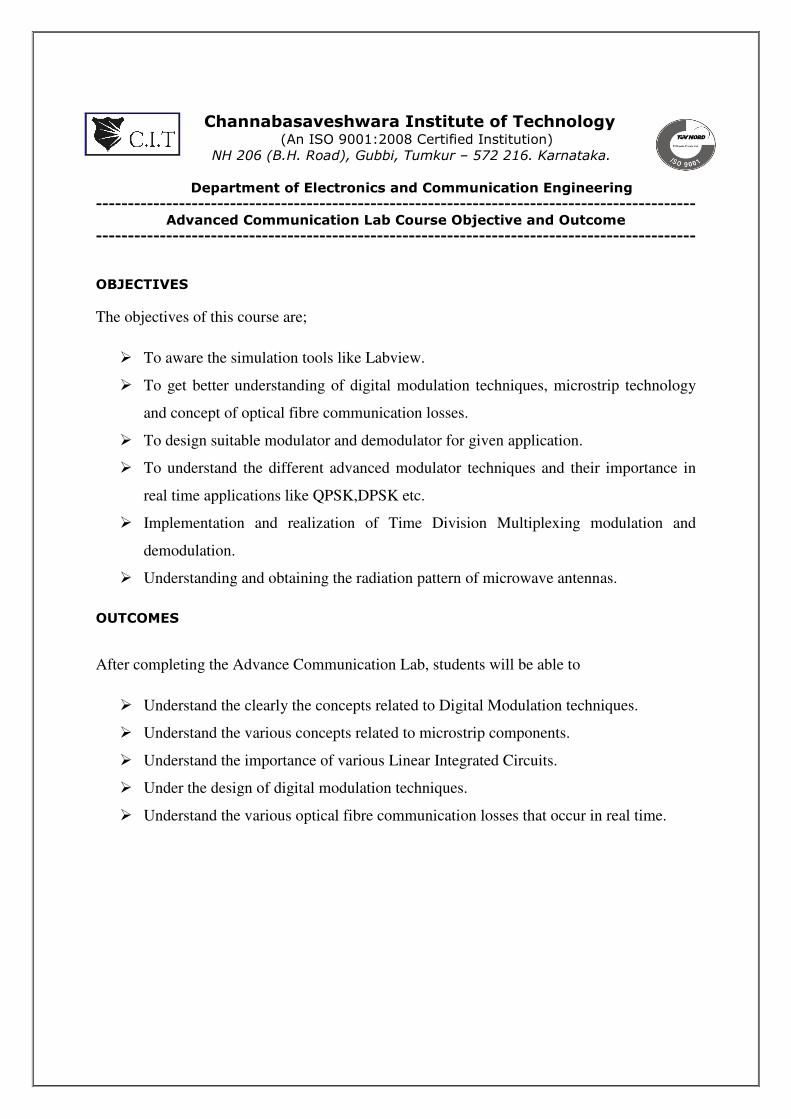
Channabasaveshwara Institute of Technology (An ISO 9001:2008 Certified Institution)
NH 206 (B.H. Road), Gubbi, Tumkur – 572 216. Karnataka.
Department of Electronics and Communication Engineering
----------------------------------------------------------------------------------------------
Advanced Communication Lab Course Objective and Outcome
----------------------------------------------------------------------------------------------
OBJECTIVES
The objectives of this course are;
To aware the simulation tools like Labview.
To get better understanding of digital modulation techniques, microstrip technology
and concept of optical fibre communication losses.
To design suitable modulator and demodulator for given application.
To understand the different advanced modulator techniques and their importance in
real time applications like QPSK,DPSK etc.
Implementation and realization of Time Division Multiplexing modulation and
demodulation.
Understanding and obtaining the radiation pattern of microwave antennas.
OUTCOMES
After completing the Advance Communication Lab, students will be able to
Understand the clearly the concepts related to Digital Modulation techniques.
Understand the various concepts related to microstrip components.
Understand the importance of various Linear Integrated Circuits.
Under the design of digital modulation techniques.
Understand the various optical fibre communication losses that occur in real time.
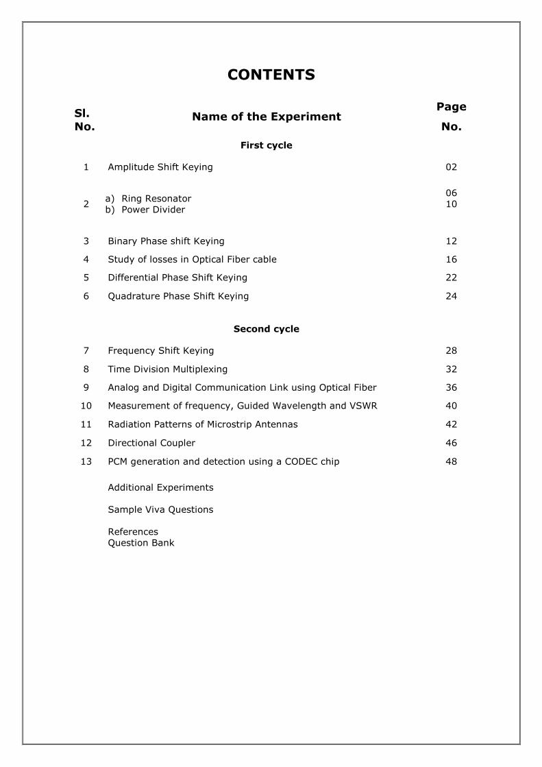
CONTENTS
Sl.
No. Name of the Experiment
Page
No.
First cycle
1 Amplitude Shift Keying 02
2 a) Ring Resonator
b) Power Divider
06
10
3 Binary Phase shift Keying 12
4 Study of losses in Optical Fiber cable 16
5 Differential Phase Shift Keying 22
6 Quadrature Phase Shift Keying 24
Second cycle
7 Frequency Shift Keying 28
8 Time Division Multiplexing 32
9 Analog and Digital Communication Link using Optical Fiber 36
10 Measurement of frequency, Guided Wavelength and VSWR 40
11 Radiation Patterns of Microstrip Antennas 42
12 Directional Coupler 46
13 PCM generation and detection using a CODEC chip 48
Additional Experiments
Sample Viva Questions
References
Question Bank
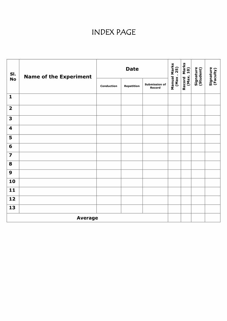
INDEX PAGEINDEX PAGEINDEX PAGEINDEX PAGE
Sl.
No Name of the Experiment
Date
Man
ual
Marks
(M
ax .
25
)
Reco
rd
M
arks
(M
ax.
10
)
Sig
natu
re
(S
tud
en
t)
Sig
natu
re
(Facu
lty)
Conduction Repetition Submission of
Record
1
2
3
4
5
6
7
8
9
10
11
12
13
Average
10ECL67-Advanced Communication Lab 2015-16
Dept. of ECE, CIT, Gubbi Page No. 1
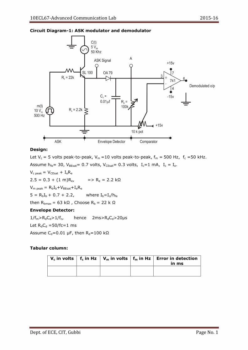
Circuit Diagram-1: ASK modulator and demodulator
Design:
Let Vc = 5 volts peak-to-peak, Vm =10 volts peak-to-peak, fm = 500 Hz, fc =50 kHz.
Assume hfe= 30, VBEsat= 0.7 volts, VCEsat= 0.3 volts, Ic=1 mA, Ic = Ie.
Vc peak = VCEsat + IeRe
2.5 = 0.3 + (1 m)Re, => Re = 2.2 kΩ
Vm peak = RbIb+VBEsat+IeRe
5 = RbIb + 0.7 + 2.2, where Ib=Ic/hfe
then Rbmax = 63 kΩ , Choose Rb = 22 k Ω
Envelope Detector:
1/fm>RdCd>1/fc, hence 2ms>RdCd>20µs
Let RdCd =50/fc=1 ms
Assume Cd=0.01 µF, then Rd=100 kΩ
Tabular column:
Vc in volts fc in Hz Vm in volts fm in Hz Error in detection in ms
10ECL67-Advanced Communication Lab 2015-16
Dept. of ECE, CIT, Gubbi Page No. 2
Experiment No. 1 Date: __ /__ / _____
AMPLITUDE SHIFT KEYING
Aim: To generate ASK signal and to demodulate it.
Apparatus Required:
Sl. No. Apparatus Range Quantity
1 Op-Amp IC 741 1
2 Transistor SL 100 1
3 Diode OA 79 1
4 Resistors As Per the design
5 Potentiometer 10KΩ 1
6 Capacitor 0.01µF 1
Procedure:
1. Connections are made as shown in the circuit diagram-1.
2. Apply a square wave modulating signal of 500 Hz (1000bits/sec) of 10VP-P
3. Apply a sine wave carrier signal of 50 kHz of 5V peak-to-peak amplitude.
4. Observe ASK waveform at point A.
5. Demodulate the ASK signal using the envelope detector.
6. To find minimum frequency of carrier signal for proper detection:
After Step 5 start reducing the frequency of the sine wave carrier signal from 50 kHz
gradually. At a particular frequency of carrier signal, the demodulated signal does not
tally with the modulating square wave. Note the carrier frequency just before the
mismatch.
10ECL67-Advanced Communication Lab
Dept. of ECE, CIT, Gubbi
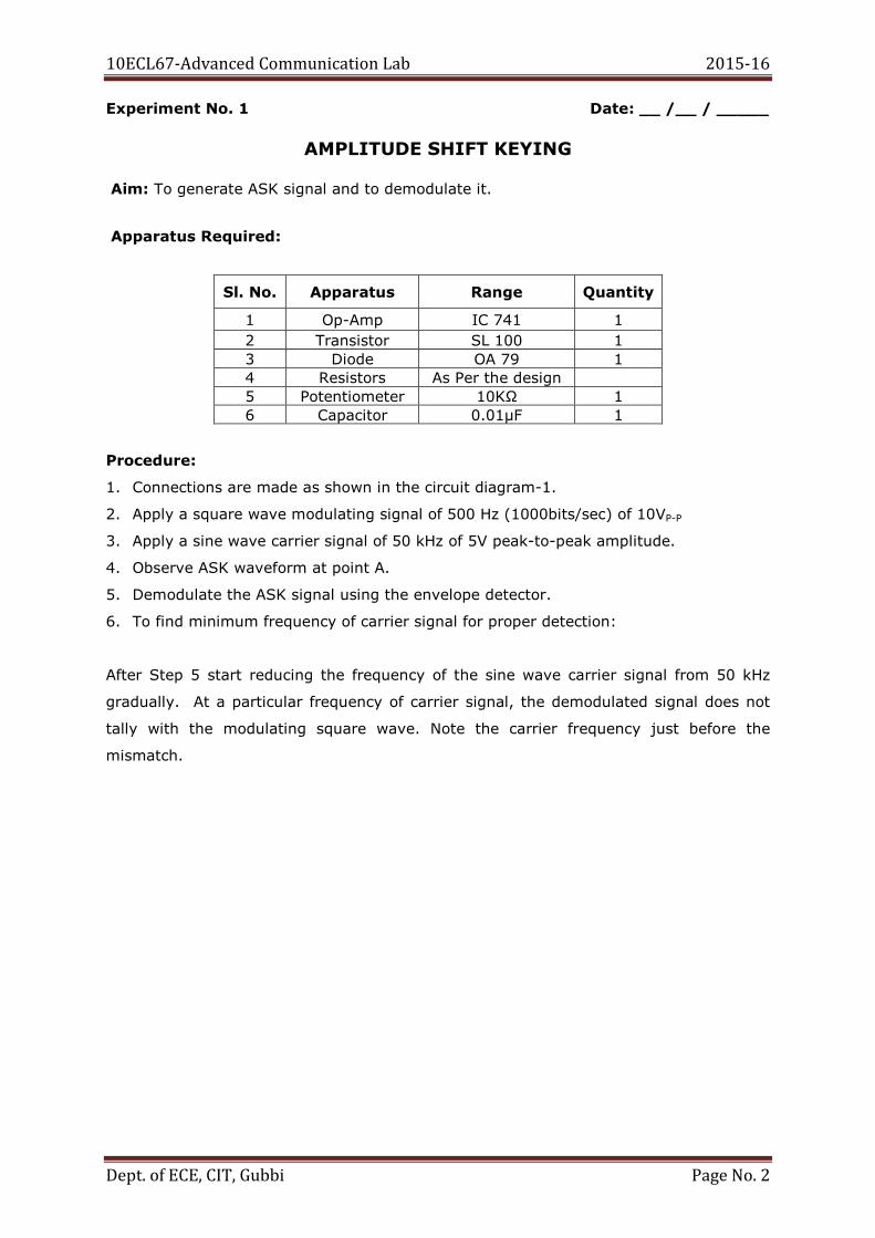
ASK modulation and demodulation waveforms
nced Communication Lab
ASK modulation and demodulation waveforms :
2015-16
Page No. 3
10ECL67-Advanced Communication Lab 2015-16
Dept. of ECE, CIT, Gubbi Page No. 4
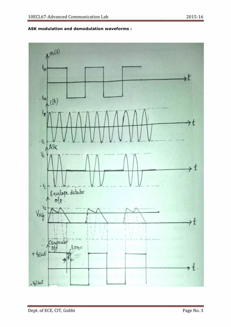
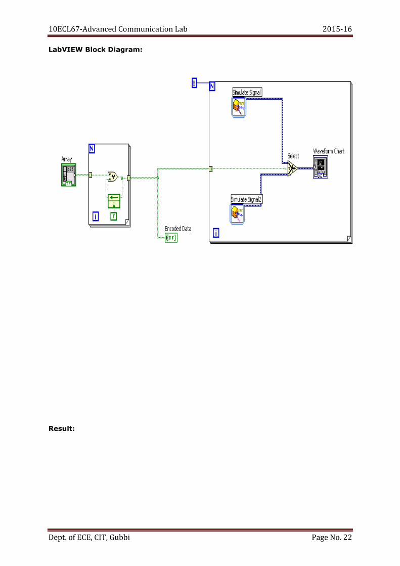
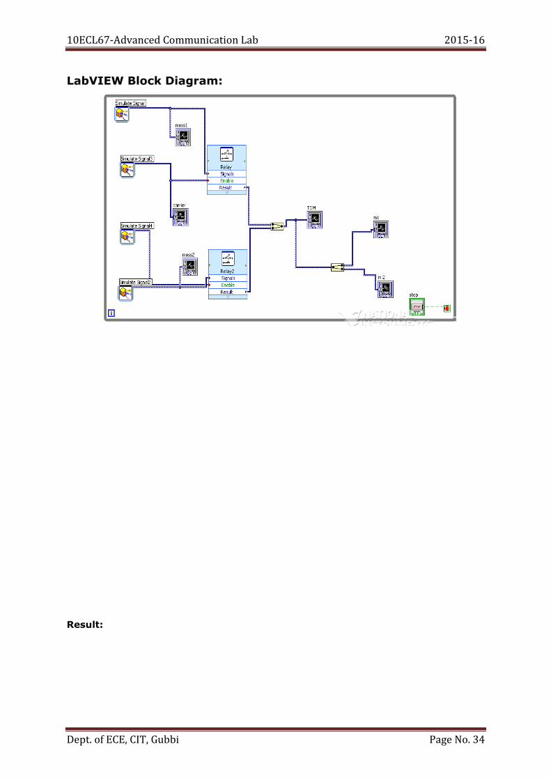
LabVIEW Block Diagram:
Result:
Error = ….….…. ms
Minimum frequency for proper detection: ………….Hz
10ECL67-Advanced Communication Lab
Dept. of ECE, CIT, Gubbi
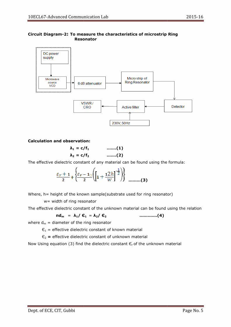
Circuit Diagram-2: To measure the characteristics of microstrip Resonator
Calculation and observation:
λ1 = c/f
λ2 = c/f
The effective dielectric constant of any material can be found using the formula:
Where, h= height of the known sample(substrate used for ring resonator)
w= width of ring resonator
The effective dielectric constant of the unknown material can be found using the relation
πdm = λ1/ Є
where dm = diameter of the ring resonator
Є1 = effective dielectric constant o
Є2 = effective dielectric constant of unknown material
Now Using equation (3) find the dielectric constant Є
nced Communication Lab
o measure the characteristics of microstrip esonator
Calculation and observation:
c/f1 …….(1)
= c/f2 …….(2)
The effective dielectric constant of any material can be found using the formula:
………(3)
Where, h= height of the known sample(substrate used for ring resonator)
width of ring resonator
The effective dielectric constant of the unknown material can be found using the relation
/ Є1 = λ2/ Є2 ………….(4)
= diameter of the ring resonator
= effective dielectric constant of known material
effective dielectric constant of unknown material
Now Using equation (3) find the dielectric constant Єr of the unknown material
2015-16
Page No. 5
o measure the characteristics of microstrip Ring
The effective dielectric constant of any material can be found using the formula:
Where, h= height of the known sample(substrate used for ring resonator)
The effective dielectric constant of the unknown material can be found using the relation
of the unknown material
10ECL67-Advanced Communication Lab 2015-16
Dept. of ECE, CIT, Gubbi Page No. 6
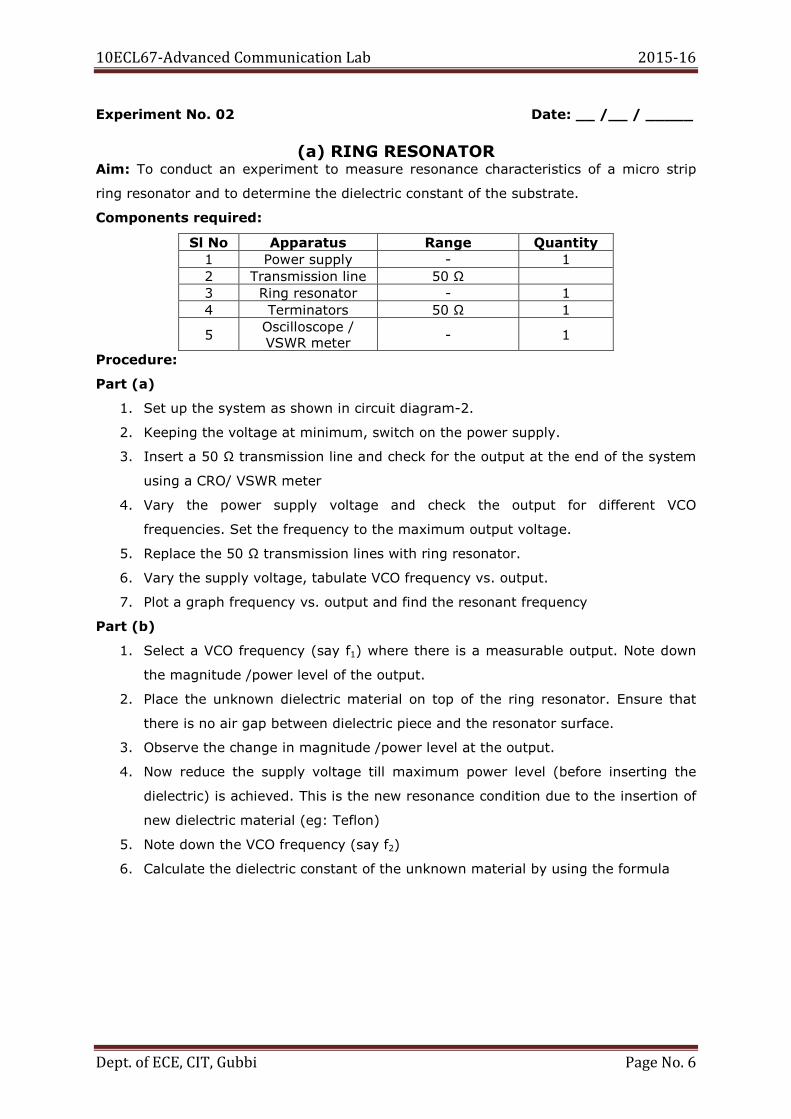
Experiment No. 02 Date: __ /__ / _____
(a) RING RESONATOR
Aim: To conduct an experiment to measure resonance characteristics of a micro strip
ring resonator and to determine the dielectric constant of the substrate.
Components required:
Sl No Apparatus Range Quantity 1 Power supply - 1
2 Transmission line 50 Ω
3 Ring resonator - 1
4 Terminators 50 Ω 1
5 Oscilloscope /
VSWR meter - 1
Procedure:
Part (a)
1. Set up the system as shown in circuit diagram-2.
2. Keeping the voltage at minimum, switch on the power supply.
3. Insert a 50 Ω transmission line and check for the output at the end of the system
using a CRO/ VSWR meter
4. Vary the power supply voltage and check the output for different VCO
frequencies. Set the frequency to the maximum output voltage.
5. Replace the 50 Ω transmission lines with ring resonator.
6. Vary the supply voltage, tabulate VCO frequency vs. output.
7. Plot a graph frequency vs. output and find the resonant frequency
Part (b)
1. Select a VCO frequency (say f1) where there is a measurable output. Note down
the magnitude /power level of the output.
2. Place the unknown dielectric material on top of the ring resonator. Ensure that
there is no air gap between dielectric piece and the resonator surface.
3. Observe the change in magnitude /power level at the output.
4. Now reduce the supply voltage till maximum power level (before inserting the
dielectric) is achieved. This is the new resonance condition due to the insertion of
new dielectric material (eg: Teflon)
5. Note down the VCO frequency (say f2)
6. Calculate the dielectric constant of the unknown material by using the formula
10ECL67-Advanced Communication Lab 2015-16
Dept. of ECE, CIT, Gubbi Page No. 7
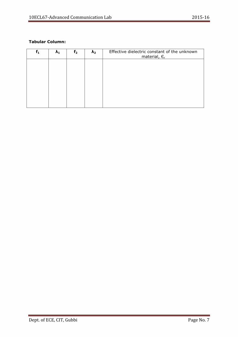
Tabular Column:
f1 λ1 f2 λ2 Effective dielectric constant of the unknown
material, Єr
10ECL67-Advanced Communication Lab 2015-16
Dept. of ECE, CIT, Gubbi Page No. 8
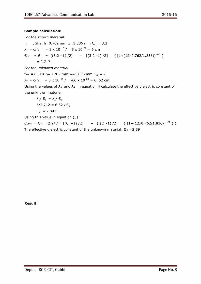
Sample calculation:
For the known material:
f1 = 5GHz, h=0.762 mm w=1.836 mm Єr1 = 3.2
λ1 = c/f1 = 3 x 10 10 / 5 x 10 09 = 6 cm
Єeff 1 = Є1 = [(3.2 +1) /2] + [(3.2 -1) /2] [1+(12x0.762/1.836)]-1/2
= 2.717
For the unknown material
f2= 4.6 GHz h=0.762 mm w=1.836 mm Єr2 = ?
λ2 = c/f2 = 3 x 10 10 / 4.6 x 10 09 = 6. 52 cm
Using the values of λ1 and λ2 in equation 4 calculate the effective dielectric constant of
the unknown material
λ1/ Є1 = λ2/ Є2
6/2.712 = 6.52 / Є2
Є2 = 2.947
Using this value in equation (3)
Єeff 2 = Є2 =2.947= [(Єr +1) /2] + ([(Єr -1) /2] [1+(12x0.762/1.836)]-1/2 )
The effective dielectric constant of the unknown material, Єr2 =2.59
Result:
10ECL67-Advanced Communication Lab
Dept. of ECE, CIT, Gubbi
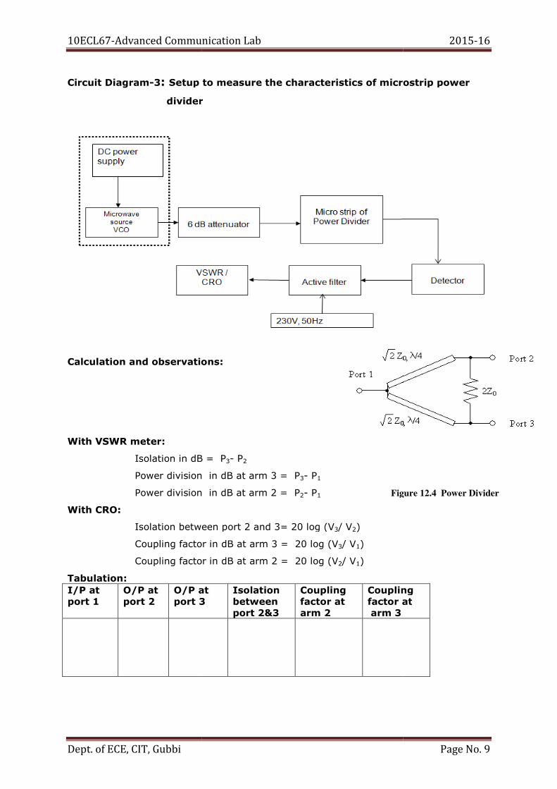
Circuit Diagram-3: Setup to measure the characteristics of
divider
Calculation and observations:
With VSWR meter:
Isolation in dB = P
Power division in dB at arm 3 = P
Power division in dB at arm 2 = P
With CRO:
Isolation between port 2 and 3= 20 log (V
Coupling factor in dB at arm 3 = 20 log (V
Coupling factor in dB at arm 2 = 20 log (V
Tabulation: I/P at port 1
O/P at port 2
O/P at port 3
nced Communication Lab
Setup to measure the characteristics of microstrip power
divider
Calculation and observations:
Isolation in dB = P3- P2
Power division in dB at arm 3 = P3- P1
Power division in dB at arm 2 = P2- P1
between port 2 and 3= 20 log (V3/ V2)
Coupling factor in dB at arm 3 = 20 log (V3/ V1)
Coupling factor in dB at arm 2 = 20 log (V2/ V1)
O/P at port 3
Isolation between port 2&3
Coupling factor at arm 2
Couplingfactor at arm 3
Figure 1
2015-16
Page No. 9
microstrip power
Coupling factor at
Figure 12.4 Power Divider
10ECL67-Advanced Communication Lab 2015-16
Dept. of ECE, CIT, Gubbi Page No. 10
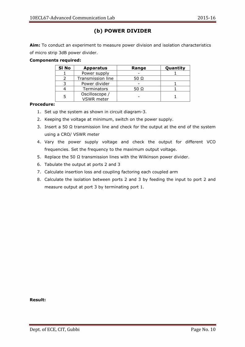
(b) POWER DIVIDER
Aim: To conduct an experiment to measure power division and isolation characteristics
of micro strip 3dB power divider.
Components required:
Sl No Apparatus Range Quantity 1 Power supply - 1
2 Transmission line 50 Ω
3 Power divider - 1
4 Terminators 50 Ω 1
5 Oscilloscope /
VSWR meter - 1
Procedure:
1. Set up the system as shown in circuit diagram-3.
2. Keeping the voltage at minimum, switch on the power supply.
3. Insert a 50 Ω transmission line and check for the output at the end of the system
using a CRO/ VSWR meter
4. Vary the power supply voltage and check the output for different VCO
frequencies. Set the frequency to the maximum output voltage.
5. Replace the 50 Ω transmission lines with the Wilkinson power divider.
6. Tabulate the output at ports 2 and 3
7. Calculate insertion loss and coupling factoring each coupled arm
8. Calculate the isolation between ports 2 and 3 by feeding the input to port 2 and
measure output at port 3 by terminating port 1.
Result:
10ECL67-Advanced Communication Lab 2015-16
Dept. of ECE, CIT, Gubbi Page No. 11
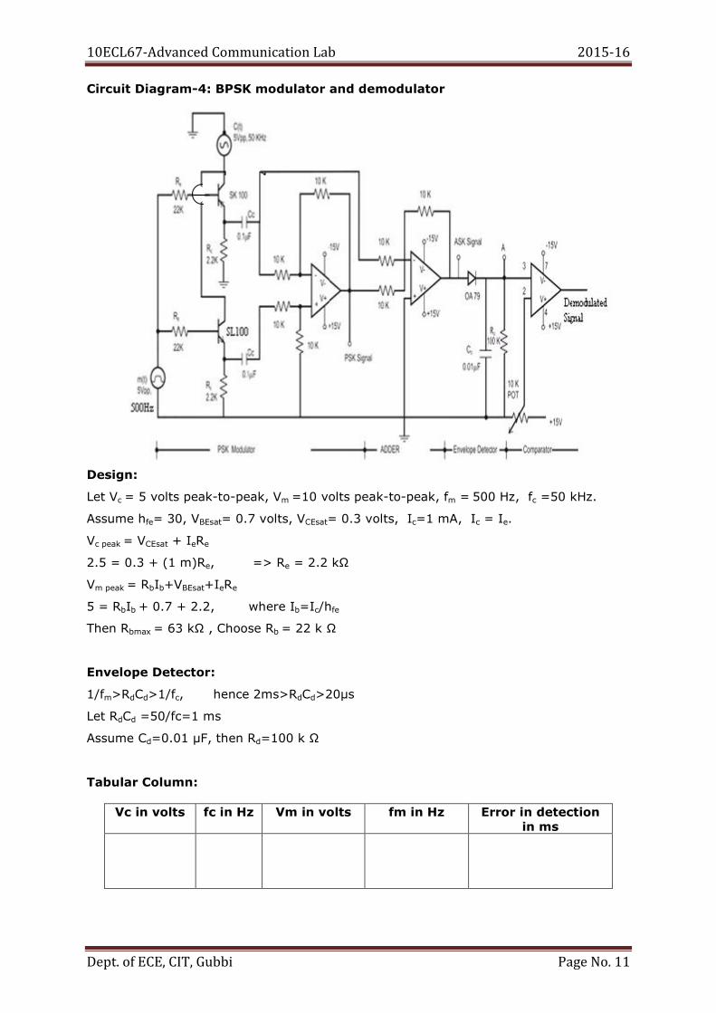
Circuit Diagram-4: BPSK modulator and demodulator
Design:
Let Vc = 5 volts peak-to-peak, Vm =10 volts peak-to-peak, fm = 500 Hz, fc =50 kHz.
Assume hfe= 30, VBEsat= 0.7 volts, VCEsat= 0.3 volts, Ic=1 mA, Ic = Ie.
Vc peak = VCEsat + IeRe
2.5 = 0.3 + (1 m)Re, => Re = 2.2 kΩ
Vm peak = RbIb+VBEsat+IeRe
5 = RbIb + 0.7 + 2.2, where Ib=Ic/hfe
Then Rbmax = 63 kΩ , Choose Rb = 22 k Ω
Envelope Detector:
1/fm>RdCd>1/fc, hence 2ms>RdCd>20µs
Let RdCd =50/fc=1 ms
Assume Cd=0.01 µF, then Rd=100 k Ω
Tabular Column:
Vc in volts fc in Hz Vm in volts fm in Hz Error in detection in ms
10ECL67-Advanced Communication Lab 2015-16
Dept. of ECE, CIT, Gubbi Page No. 12
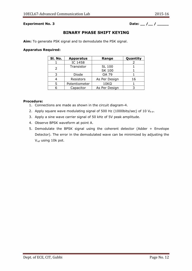
Experiment No. 3 Date: __ /__ / _____
BINARY PHASE SHIFT KEYING
Aim: To generate PSK signal and to demodulate the PSK signal.
Apparatus Required:
Sl. No. Apparatus Range Quantity 1 IC 1458 2
2 Transistor
SL 100
SK 100
1
1
3 Diode OA 79 1
4 Resistors As Per Design 16
5 Potentiometer 10KΩ 1
6 Capacitor As Per Design 3
Procedure:
1. Connections are made as shown in the circuit diagram-4.
2. Apply square wave modulating signal of 500 Hz (1000bits/sec) of 10 VP-P.
3. Apply a sine wave carrier signal of 50 kHz of 5V peak amplitude.
4. Observe BPSK waveform at point A.
5. Demodulate the BPSK signal using the coherent detector (Adder + Envelope
Detector). The error in the demodulated wave can be minimized by adjusting the
Vref using 10k pot.
10ECL67-Advanced Communication Lab
Dept. of ECE, CIT, Gubbi
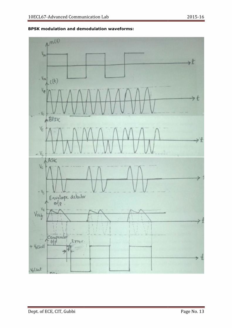
BPSK modulation and demodulation waveforms
nced Communication Lab
BPSK modulation and demodulation waveforms:
2015-16
Page No. 13
10ECL67-Advanced Communication Lab 2015-16
Dept. of ECE, CIT, Gubbi Page No. 14
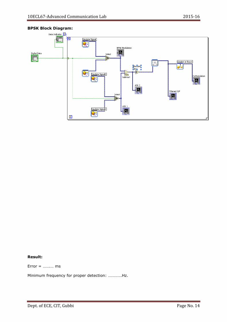
BPSK Block Diagram:
Result:
Error = …….… ms
Minimum frequency for proper detection: ………….Hz.
10ECL67-Advanced Communication Lab 2015-16
Dept. of ECE, CIT, Gubbi Page No. 15
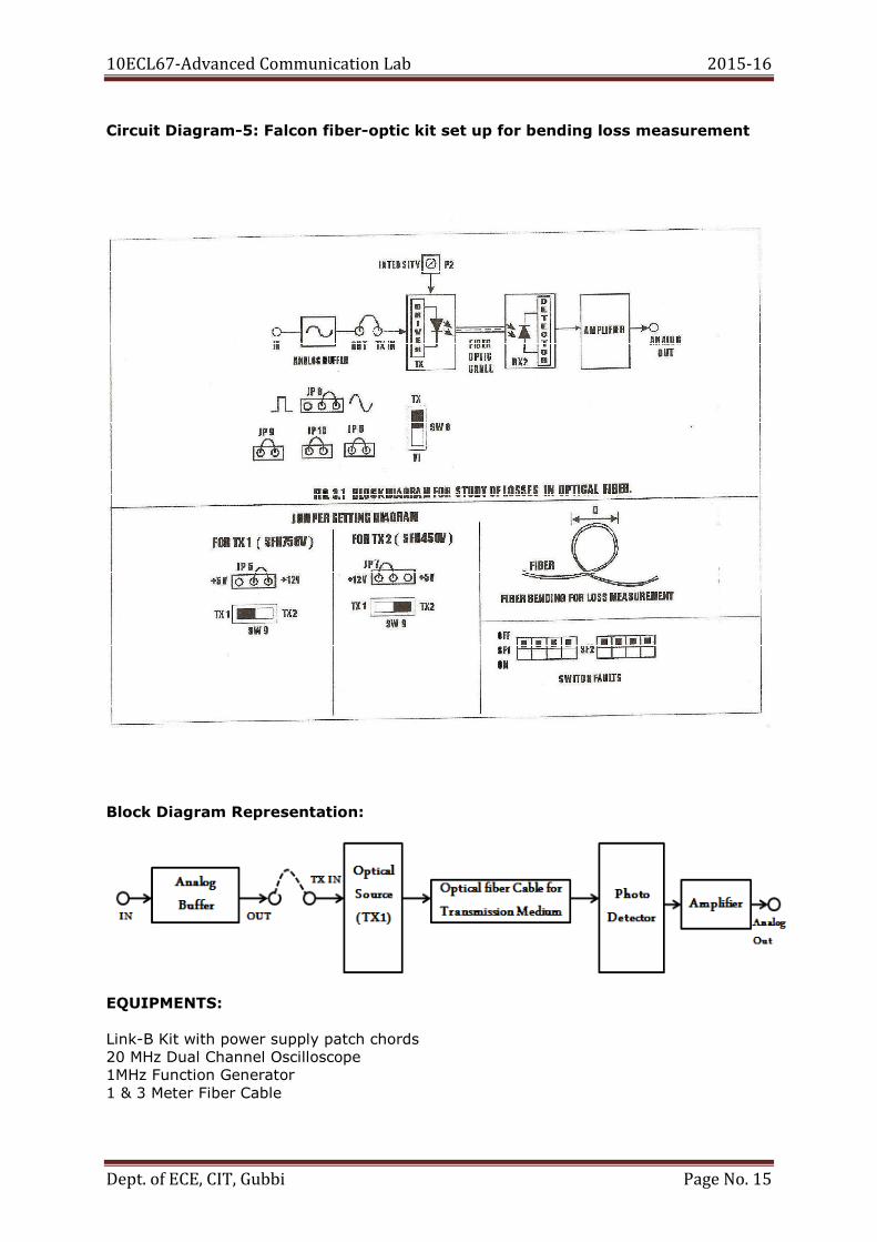
Circuit Diagram-5: Falcon fiber-optic kit set up for bending loss measurement
Block Diagram Representation:
EQUIPMENTS:
Link-B Kit with power supply patch chords
20 MHz Dual Channel Oscilloscope
1MHz Function Generator
1 & 3 Meter Fiber Cable
10ECL67-Advanced Communication Lab 2015-16
Dept. of ECE, CIT, Gubbi Page No. 16
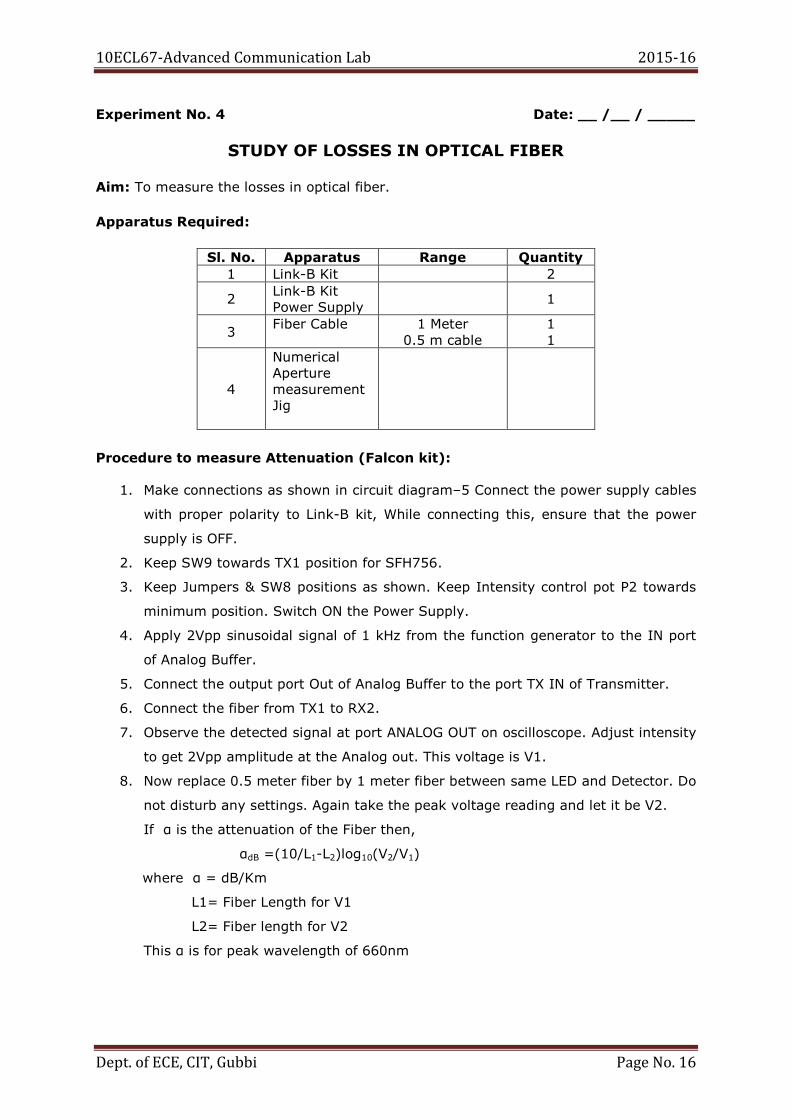
Experiment No. 4 Date: __ /__ / _____
STUDY OF LOSSES IN OPTICAL FIBER
Aim: To measure the losses in optical fiber.
Apparatus Required:
Sl. No. Apparatus Range Quantity 1 Link-B Kit 2
2 Link-B Kit
Power Supply 1
3 Fiber Cable
1 Meter
0.5 m cable
1
1
4
Numerical
Aperture
measurement
Jig
Procedure to measure Attenuation (Falcon kit):
1. Make connections as shown in circuit diagram–5 Connect the power supply cables
with proper polarity to Link-B kit, While connecting this, ensure that the power
supply is OFF.
2. Keep SW9 towards TX1 position for SFH756.
3. Keep Jumpers & SW8 positions as shown. Keep Intensity control pot P2 towards
minimum position. Switch ON the Power Supply.
4. Apply 2Vpp sinusoidal signal of 1 kHz from the function generator to the IN port
of Analog Buffer.
5. Connect the output port Out of Analog Buffer to the port TX IN of Transmitter.
6. Connect the fiber from TX1 to RX2.
7. Observe the detected signal at port ANALOG OUT on oscilloscope. Adjust intensity
to get 2Vpp amplitude at the Analog out. This voltage is V1.
8. Now replace 0.5 meter fiber by 1 meter fiber between same LED and Detector. Do
not disturb any settings. Again take the peak voltage reading and let it be V2.
If α is the attenuation of the Fiber then,
αdB =(10/L1-L2)log10(V2/V1)
where α = dB/Km
L1= Fiber Length for V1
L2= Fiber length for V2
This α is for peak wavelength of 660nm
10ECL67-Advanced Communication Lab 2015-16
Dept. of ECE, CIT, Gubbi Page No. 17
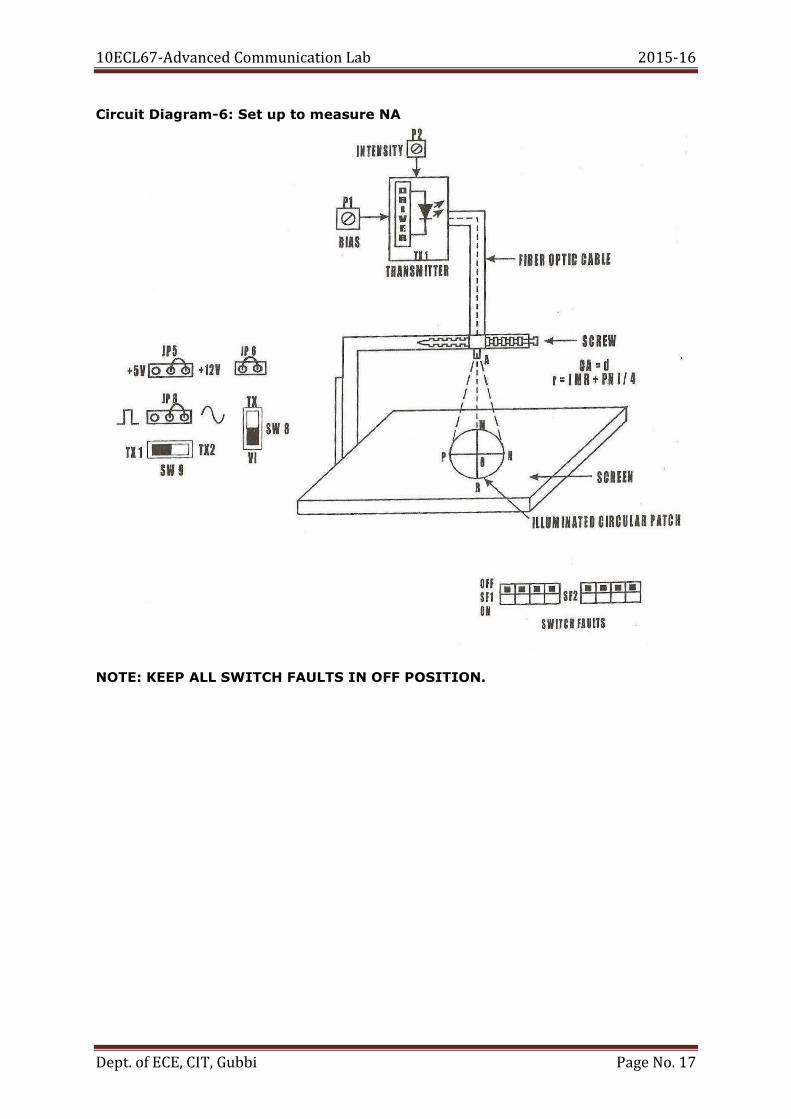
Circuit Diagram-6: Set up to measure NA
NOTE: KEEP ALL SWITCH FAULTS IN OFF POSITION.
10ECL67-Advanced Communication Lab 2015-16
Dept. of ECE, CIT, Gubbi Page No. 18
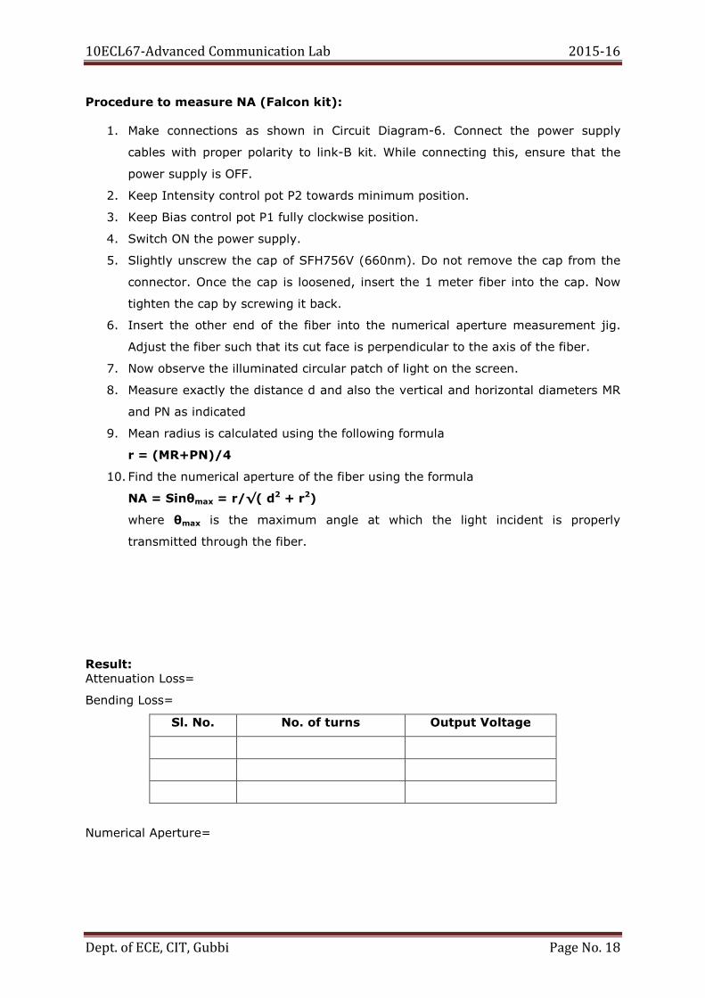
Procedure to measure NA (Falcon kit):
1. Make connections as shown in Circuit Diagram-6. Connect the power supply
cables with proper polarity to link-B kit. While connecting this, ensure that the
power supply is OFF.
2. Keep Intensity control pot P2 towards minimum position.
3. Keep Bias control pot P1 fully clockwise position.
4. Switch ON the power supply.
5. Slightly unscrew the cap of SFH756V (660nm). Do not remove the cap from the
connector. Once the cap is loosened, insert the 1 meter fiber into the cap. Now
tighten the cap by screwing it back.
6. Insert the other end of the fiber into the numerical aperture measurement jig.
Adjust the fiber such that its cut face is perpendicular to the axis of the fiber.
7. Now observe the illuminated circular patch of light on the screen.
8. Measure exactly the distance d and also the vertical and horizontal diameters MR
and PN as indicated
9. Mean radius is calculated using the following formula
r = (MR+PN)/4
10. Find the numerical aperture of the fiber using the formula
NA = Sinθmax = r/√( d2 + r2)
where θmax is the maximum angle at which the light incident is properly
transmitted through the fiber.
Result: Attenuation Loss=
Bending Loss=
Sl. No. No. of turns Output Voltage
Numerical Aperture=
10ECL67-Advanced Communication Lab 2015-16
Dept. of ECE, CIT, Gubbi Page No. 19
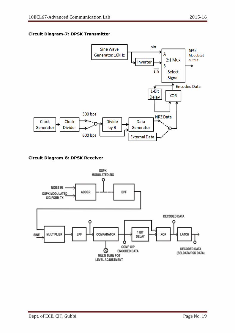
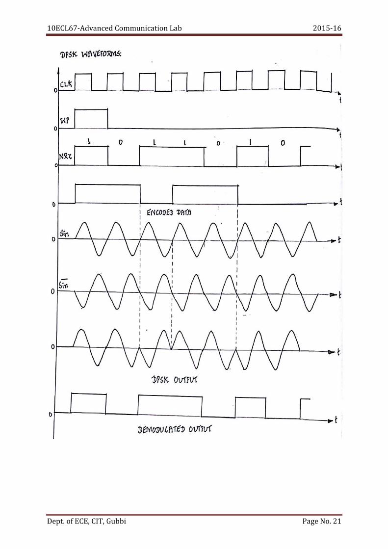
Circuit Diagram-7: DPSK Transmitter
Circuit Diagram-8: DPSK Receiver
10ECL67-Advanced Communication Lab 2015-16
Dept. of ECE, CIT, Gubbi Page No. 20
Experiment No. 5 Date: __ /__ / _____
DIFFERENTIAL PHASE SHIFT KEYING
Aim: Study of Carrier Modulation Techniques by DPSK.
Apparatus Required:
Sl. No. Apparatus Range Quantity 1 DPSK Kit Kit No. 1
2 Power Supply 1
3 Patch Cards
Procedure for Transmitter:
1. Switch on the power supply.
2. Connect either 300 or 600 bps clock to SEL CLK socket, connect measuring probe of
CRO to SEL CLK and WORDPULSE to observe the selected clock (300bps or 600bps).
3. Connect MARK (Sine) and MARK (SINE) Mux input.
4. Connect NRZ DATA to SEL DATA. Adjust the dip switch to any digital patterns of 8
bits by keeping them for ‘1’ or ‘0’ positions also observe selected data in CRO.
5. Connect DPSK data to Mux input, also observe DPSK data.
Procedure for Receiver:
1. Interconnect the Transmitter and Receiver modules through the interconnecting cable
required.
2. Connect Adder output to BPF input.
3. If external clock is required give from SEL CLK from Tx socket.
4. If External carrier is required, feed it from CARRIER FROM Tx socket.
5. Observe the modulated signal at DPSK IN, DPSK O/P in the CRO. The output should
match the data transmitted from the transmitter.
10ECL67-Advanced Communication Lab 2015-16
Dept. of ECE, CIT, Gubbi Page No. 21
10ECL67-Advanced Communication Lab 2015-16
Dept. of ECE, CIT, Gubbi Page No. 22
LabVIEW Block Diagram:
Result:
10ECL67-Advanced Communication Lab 2015-16
Dept. of ECE, CIT, Gubbi Page No. 23
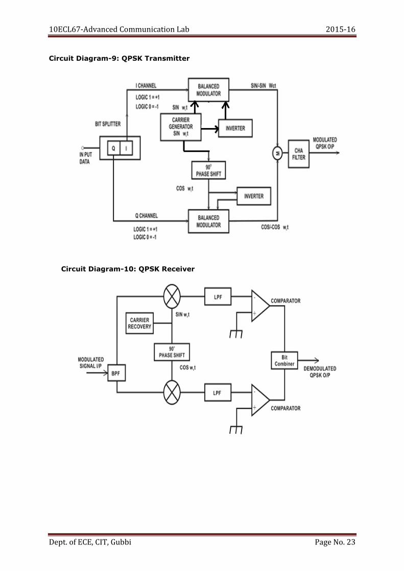
Circuit Diagram-9: QPSK Transmitter
Circuit Diagram-10: QPSK Receiver
10ECL67-Advanced Communication Lab 2015-16
Dept. of ECE, CIT, Gubbi Page No. 24
Experiment No. 6 Date: __ /__ / _____
QUADRATURE PHASE SHIFT KEYING
Aim: Study of Carrier Modulation Techniques by QPSK method.
Apparatus Required:
Sl. No. Apparatus Range Quantity 1 QPSK Kit Kit no. 1
2 Power Supply 1
3 Patch Cards
Procedure for Transmitter:
1. Switch on the power supply from power cord to module given.
2. Connect either 300 or 600 bps clock to SEL CLK Socket, connect measuring probe of
CRO to SEL CLK and WORDPULSE to observe the selected clock (300 or 600 bps).
3. Connect NRZ or EXT DATA to SEL DATA. Adjust the dip switch to any digital patterns
of 8 bits by keeping them for ‘1’ or ‘0’ positions. Observe the selected data in CRO.
4. Separately monitor the selected data, word pulse (WP) by connecting WP to A
Channel of CRO and selected data to B Channel of CRO.
5. Monitor selected data in channel A of CRO and Compare it with B∅ and B1 on
channel B. Observe QPSK output according to phase change on output according to
B∅ and B1.
Procedure for Receiver:
1. Connect Transmitter and Receiver with interconnecting cable required.
2. Check the WP, Sin, Cos, B∅, B1 and QPSK output on Transmitter.
3. Check the QPSK Signal at receiver at pin input SIGNAL.
4. Connecting SIGNAL to Channel A of CRO and verify the waveform by connecting the
Channel B to PRE B∅, PRE B1 and QPSK output. The waveform of PRE B∅ should
correspond to B∅ of Transmitter and the waveform of PRE B1 should correspond to
B1 of Transmitter. The QPSK output should correspond to NRZ (L) of transmitter.
10ECL67-Advanced Communication Lab
Dept. of ECE, CIT, Gubbi
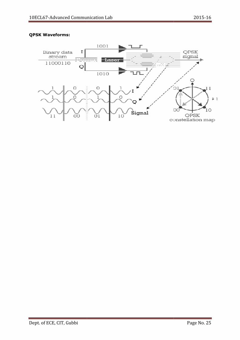
QPSK Waveforms:
nced Communication Lab
2015-16
Page No. 25
10ECL67-Advanced Communication Lab 2015-16
Dept. of ECE, CIT, Gubbi Page No. 26
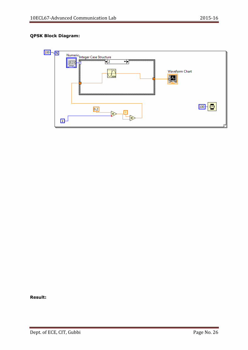
QPSK Block Diagram:
Result:
10ECL67-Advanced Communication Lab 2015-16
Dept. of ECE, CIT, Gubbi Page No. 27
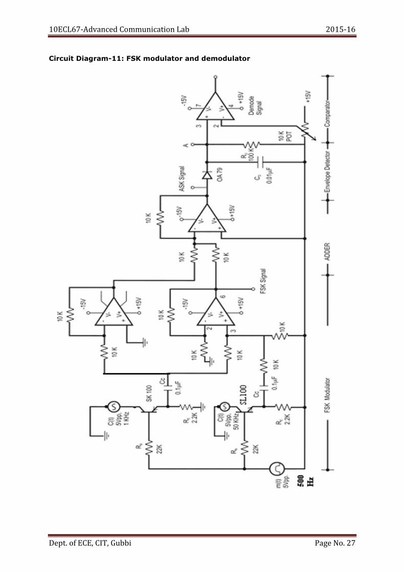
Circuit Diagram-11: FSK modulator and demodulator
10ECL67-Advanced Communication Lab 2015-16
Dept. of ECE, CIT, Gubbi Page No. 28
Experiment No. 7 Date: __ /__ / _____
FREQUENCY SHIFT KEYING
Aim: To generate FSK signal and to demodulate the FSK signal.
Apparatus Required:
Sl.No Apparatus Range Quantity 1 IC 1458 2
2 Transistor
SL 100
SK 100
1
1
3 Diode OA 79 1
4 Resistors As Per Design 16
5 Potentiometer 10KΩ 1
6 Capacitor As Per Design 3
Procedure:
1. Connections are made as shown in circuit diagram-11.
2. Apply a square wave modulating signal of 100 Hz (200bits/sec) and 10 VP-P
amplitude.
3. Apply a sine wave carrier signal-1 of 1 kHz, 5V peak to peak amplitude and signal-2
of 50 kHz, 5V peak to peak amplitude.
4. Observe FSK waveform at point A.
5. Demodulate the FSK signal using the coherent detector (Adder + Envelope Detector).
The error in the demodulated waveform can be minimized by adjusting the Vref using
10k POT.
10ECL67-Advanced Communication Lab
Dept. of ECE, CIT, Gubbi
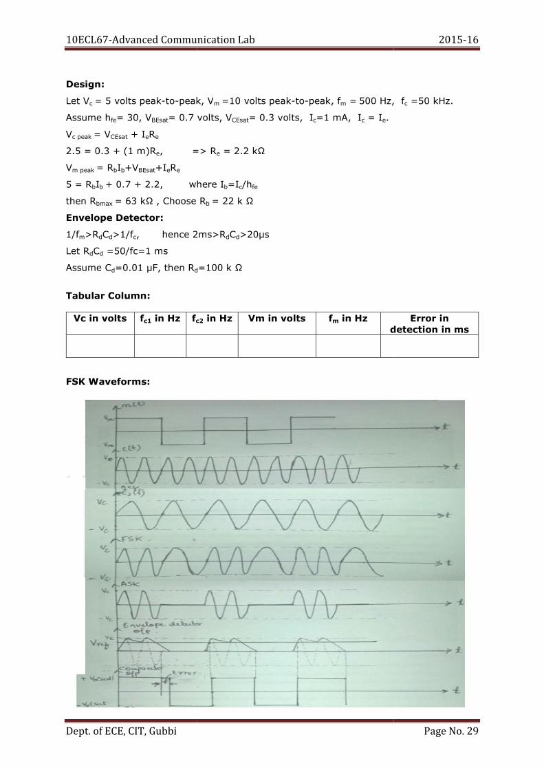
Design:
Let Vc = 5 volts peak-to-peak, V
Assume hfe= 30, VBEsat= 0.7 volts, V
Vc peak = VCEsat + IeRe
2.5 = 0.3 + (1 m)Re, => R
Vm peak = RbIb+VBEsat+IeRe
5 = RbIb + 0.7 + 2.2, where I
then Rbmax = 63 kΩ , Choose R
Envelope Detector:
1/fm>RdCd>1/fc, hence 2ms>R
Let RdCd =50/fc=1 ms
Assume Cd=0.01 µF, then Rd
Tabular Column:
Vc in volts fc1 in Hz fc2
FSK Waveforms:
nced Communication Lab
peak, Vm =10 volts peak-to-peak, fm = 500 Hz, f
= 0.7 volts, VCEsat= 0.3 volts, Ic=1 mA, Ic = Ie.
, => Re = 2.2 kΩ
+ 0.7 + 2.2, where Ib=Ic/hfe
= 63 kΩ , Choose Rb = 22 k Ω
, hence 2ms>RdCd>20µs
d=100 k Ω
c2 in Hz Vm in volts fm in Hz detection in ms
2015-16
Page No. 29
500 Hz, fc =50 kHz.
= 2.2 kΩ
Error in detection in ms
10ECL67-Advanced Communication Lab 2015-16
Dept. of ECE, CIT, Gubbi Page No. 30
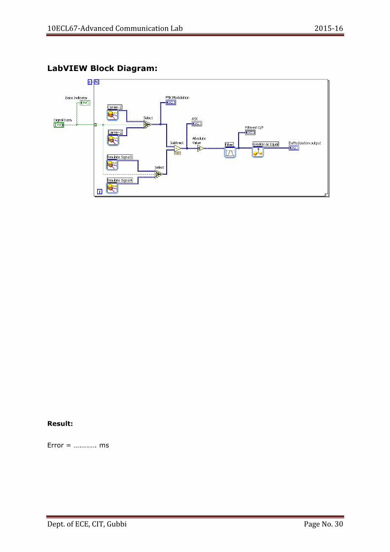
LabVIEW Block Diagram:
Result:
Error = ….….…. ms
10ECL67-Advanced Communication Lab 2015-16
Dept. of ECE, CIT, Gubbi Page No. 31
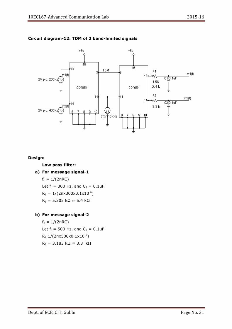
Circuit diagram-12: TDM of 2 band-limited signals
Design:
Low pass filter:
a) For message signal-1
fc = 1/(2πRC)
Let fc = 300 Hz, and C1 = 0.1µF.
R1 = 1/(2πx300x0.1x10-6)
R1 = 5.305 kΩ ≈ 5.4 kΩ
b) For message signal-2
fc = 1/(2πRC)
Let fc = 500 Hz, and C2 = 0.1µF.
R2 1/(2πx500x0.1x10-6)
R2 = 3.183 kΩ ≈ 3.3 kΩ
5.4 k
3.3 k
10ECL67-Advanced Communication Lab 2015-16
Dept. of ECE, CIT, Gubbi Page No. 32
Experiment No. 8 Date: __ /__ / _____
TIME DIVISION MULTIPLEXING
Aim: To study Time Division Multiplexing for 2 band-limited signals.
Apparatus Required:
Sl No Apparatus Range Quantity 1 IC CD 4051 2
2 Resistors As Per Design 2
3 Capacitor As Per Design 2
Procedure:
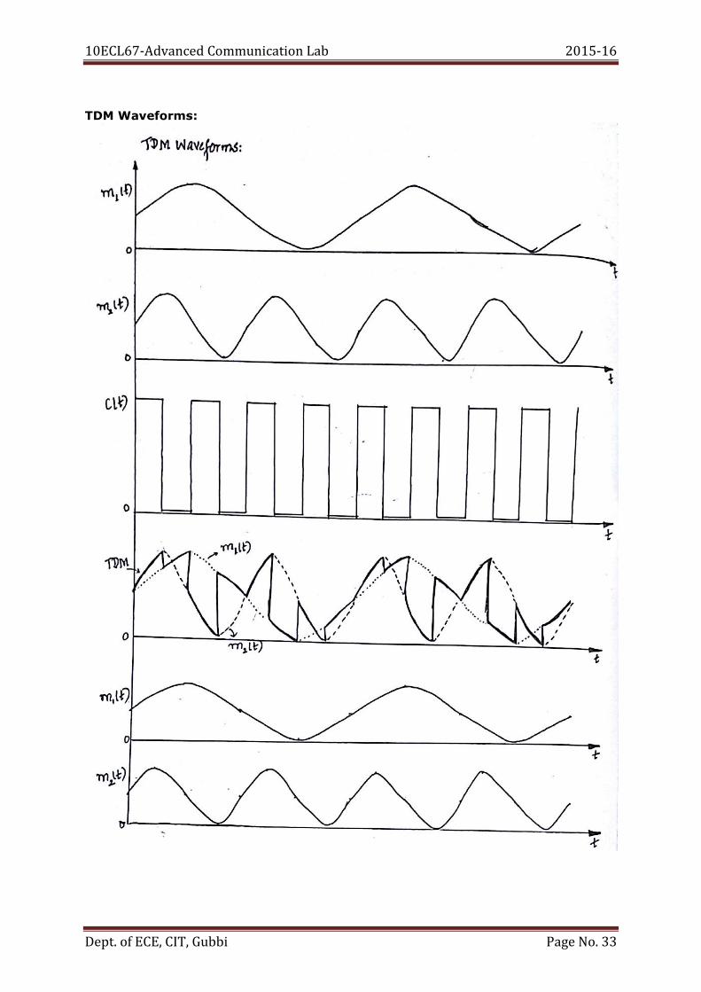
1. Connections are made as shown in the circuit diagram-12.
2. Apply a square wave (TTL) carrier signal of 2 kHz (or >2 kHz) of 5V amplitude.
3. Apply m1(t) and m2(t) whose frequencies are f1 (200 Hz, with DC offset) and f2 (400
Hz, with DC offset).
4. Observe TDM waveform at pin number 3 of IC CD4051.
5. Observe the reconstructed message waveforms m1(t) and m2(t) at pin numbers 13
and 14 of 2nd IC CD4051.
6. The ripples in the demodulated signals can be reduced by increasing the order of the
filter or by increasing the carrier frequency.
10ECL67-Advanced Communication Lab 2015-16
Dept. of ECE, CIT, Gubbi Page No. 33
TDM Waveforms:
10ECL67-Advanced Communication Lab 2015-16
Dept. of ECE, CIT, Gubbi Page No. 34
LabVIEW Block Diagram:
Result:
10ECL67-Advanced Communication Lab
Dept. of ECE, CIT, Gubbi
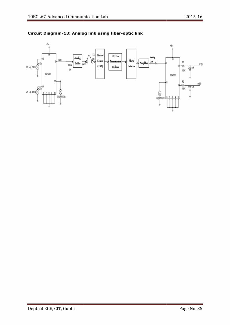
Circuit Diagram-13: Analog link using fiber
nced Communication Lab
Analog link using fiber-optic link
2015-16
Page No. 35
10ECL67-Advanced Communication Lab 2015-16
Dept. of ECE, CIT, Gubbi Page No. 36
Experiment No. 9 Date: __ /__ / _____
ANALOG AND DIGITAL COMMUNICATION LINK USING OPTICAL FIBER
Aim: The aim of this experiment is to establish analog and digital communication link
using optical fiber
Apparatus Required:
Sl No Apparatus Range Quantity
1 Link B Kit with
power supply - 1
2 Patch chords -
3 Dual trace
Oscilloscope 20MHz 1
4 Fiber cable 1 meter 1
NOTE: KEEP ALL SWITCH FAULTS IN OFF POSITION
PROCEDURE:
Make the connection as shown in circuit diagram-13. Before establishing the analog link,
obtain the TDM output from Analog 8:1 Mux.
a) ANALOG LINK
1. Make the connection as shown in the diagram, and adjust the jumper & switch
settings as shown in circuit diagram -13.
2. Keep the intensity control pot P2 towards minimum position.
3. Switch On the power supply.
4. Feed 2 Vpp sinusoidal signal of 1 kHz from the function generator to the IN port of
analog buffer.
5. Connect the OUT port of analog buffer to the TX IN of transmitter.
6. Slightly unscrew the cap of SFH756V (660 nm). Do not remove the cap from the
connector. Once the cap is loosened, insert the 1 meter Fiber into the cap. Now
tighten the cap by screwing it back.
7. Connect the other end of the fiber to the detector SFH350V (photo transistor
detector) carefully as per the instructions given in the above step.
8. Observe the detected signal at ANALOG OUT port on the oscilloscope.. adjust the
intensity control pot P2 so that a signal of a signal of 2 Vpp amplitude is received.
9. To measure the analog bandwidth of the photo transistor, vary the signal
frequency and observe the detected signal at various frequencies.
10. Plot the detected signal against applied signal frequency and determine the 3 dB
bandwidth.
10ECL67-Advanced Communication Lab 2015-16
Dept. of ECE, CIT, Gubbi Page No. 37
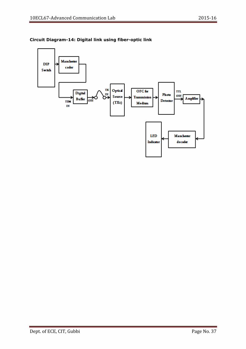
Circuit Diagram-14: Digital link using fiber-optic link
10ECL67-Advanced Communication Lab 2015-16
Dept. of ECE, CIT, Gubbi Page No. 38
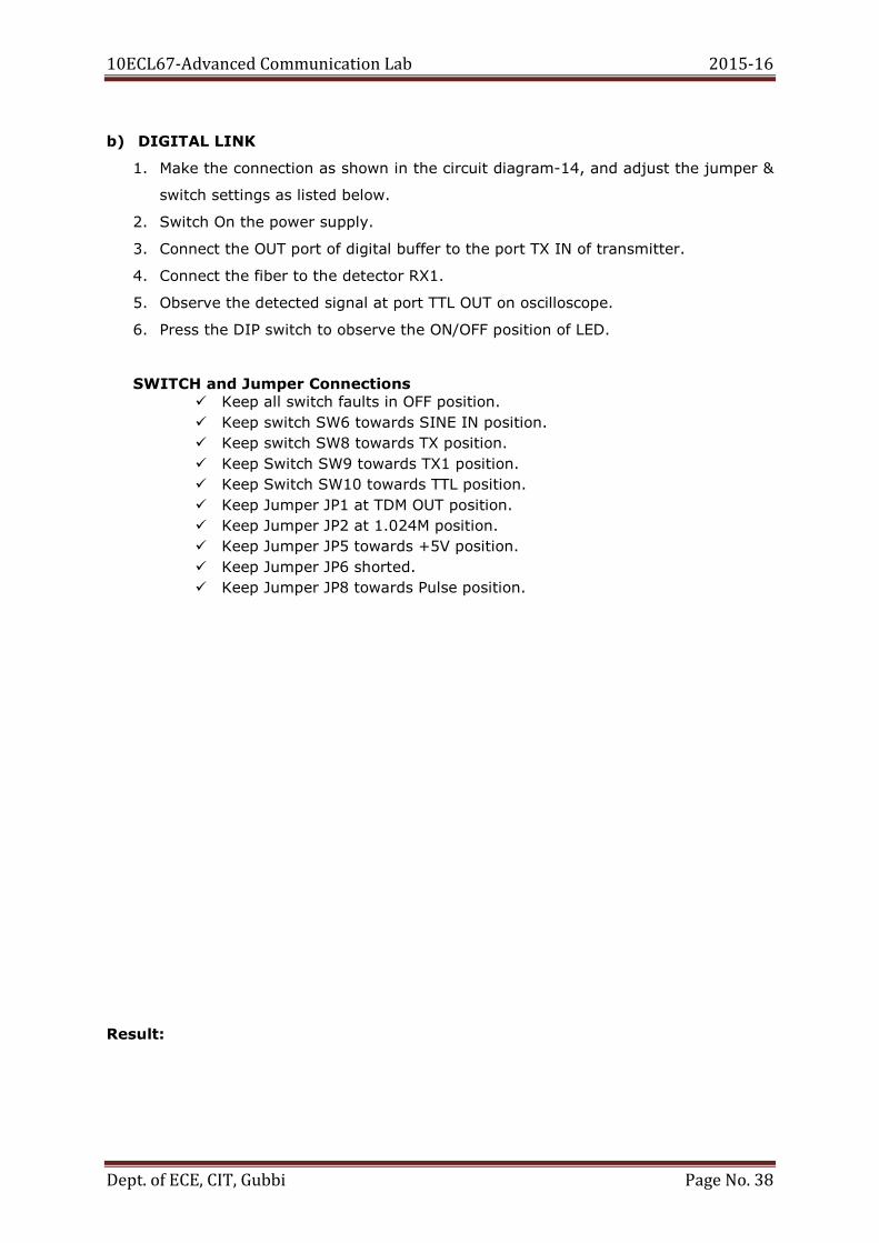
b) DIGITAL LINK
1. Make the connection as shown in the circuit diagram-14, and adjust the jumper &
switch settings as listed below.
2. Switch On the power supply.
3. Connect the OUT port of digital buffer to the port TX IN of transmitter.
4. Connect the fiber to the detector RX1.
5. Observe the detected signal at port TTL OUT on oscilloscope.
6. Press the DIP switch to observe the ON/OFF position of LED.
SWITCH and Jumper Connections Keep all switch faults in OFF position.
Keep switch SW6 towards SINE IN position.
Keep switch SW8 towards TX position.
Keep Switch SW9 towards TX1 position.
Keep Switch SW10 towards TTL position.
Keep Jumper JP1 at TDM OUT position.
Keep Jumper JP2 at 1.024M position.
Keep Jumper JP5 towards +5V position.
Keep Jumper JP6 shorted.
Keep Jumper JP8 towards Pulse position.
Result:
10ECL67-Advanced Communication Lab 2015-16
Dept. of ECE, CIT, Gubbi Page No. 39
Circuit Diagram-15: Microwave test bench set up
Waveform:
Tabular Column:
Load V max V min VSWR
Horn
Short Circuit
Open Circuit
Match Termination
X1= MSR + (CVD x LC) LC = 0.01 cm λg = 2(X1≈X2)cm = ………….,
λo = (λg x λc) 2
(λg2
+ λc2)
VSWR = Vmax/ Vmin
Load X1 X2 λg λc λ0 f0
GHz
Horn
Short Circuit
Open Circuit
Match
Termination
√
λc=2a a=2.54cm
10ECL67-Advanced Communication Lab 2015-16
Dept. of ECE, CIT, Gubbi Page No. 40
Experiment No. 10 Date: __ /__ / _____
MEASUREMENT OF FREQUENCY, λg, VSWR
Aim: To measure the frequency, guide wavelength, power and VSWR of a microwave
guide.
Procedure:
1. Set up the microwave bench as shown in circuit diagram-15.
2. With Reflector voltage in maximum position and beam voltage in minimum
position switch on the Klystron power supply (Both main and HT switch) wait until
current reaches 10 to 12mA.
3. Observe the signal at the output of the detector if it is not a square wave then
reduce the reflector voltage until a square wave signal is obtained.
4. Observe the standing wave pattern on SWG (Slotted Wave Guide), note the
maximum and minimum voltage levels of the standing wave pattern of the
connected load.
5. Note the positions of any 2 consecutive minima X1 and X2 (or maxima); twice the
difference between these will give the guide wavelength λg.
Result:
λg =…………… fo =…………….
10ECL67-Advanced Communication Lab 2015-16
Dept. of ECE, CIT, Gubbi Page No. 41
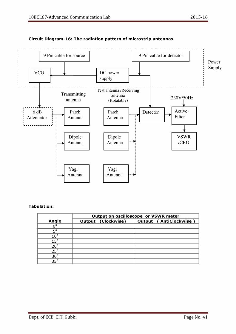
Circuit Diagram-16: The radiation pattern of microstrip antennas
Tabulation:
Angle
Output on oscilloscope or VSWR meter Output (Clockwise) Output ( AntiClockwise )
0o
5o
10o
15o
20o
25o
30o
35o
DC power
supply
Detector
VCO
Patch
Antenna
Dipole
Antenna
Dipole
Antenna
Patch
Antenna
Active
Filter
230V/50Hz
VSWR
/CRO
Yagi
Antenna
Transmitting
antenna
Test antenna /Receiving
antenna
(Rotatable)
Yagi
Antenna
9 Pin cable for source 9 Pin cable for detector
6 dB
Attenuator
Power
Supply
10ECL67-Advanced Communication Lab 2015-16
Dept. of ECE, CIT, Gubbi Page No. 42
Experiment No. 11 Date: __ /__ / _____
RADIATION PATTERN OF MICROSTRIP ANTENNAS
Aim: To conduct an experiment to obtain radiation pattern and to measure the
directivity and gain of the following antennas:
1) Standard dipole (or printed dipole)
2) Micro strip patch antenna,
3) Yagi antenna (printed)
Procedure:
1. Set up the system as shown in circuit diagram-16 for a standard dipole antenna.
2. Keeping the voltage at minimum, switch on the power the supply.
3. Vary the power supply voltage and check the output for different VCO frequencies.
The frequency at which the output becomes maximum is the resonant frequency.
4. At the resonant frequency, adjust the distance between the transmitting and receiving
antennas using the formula S=2d2 / λ
where d is the broader dimension of the antenna.
5. Keeping both the antennas in line of sight (0ο at the turn table), tabulate the output
(Et)
6. Rotate the turn table in clock-wise and anti clock-wise for different angles of
deflection and tabulate the output for every angle(Er).
7. Plot a graph of angle vs. output.
8. Find the half power beam width (HPBW) from the points where the power becomes
half (3 dB points or 0.707 V Points)
9. Calculate Directivity and gain of the antenna by using the formula.
10. Repeat the experiment for a patch antenna and a yagi antenna.
10ECL67-Advanced Communication Lab
Dept. of ECE, CIT, Gubbi
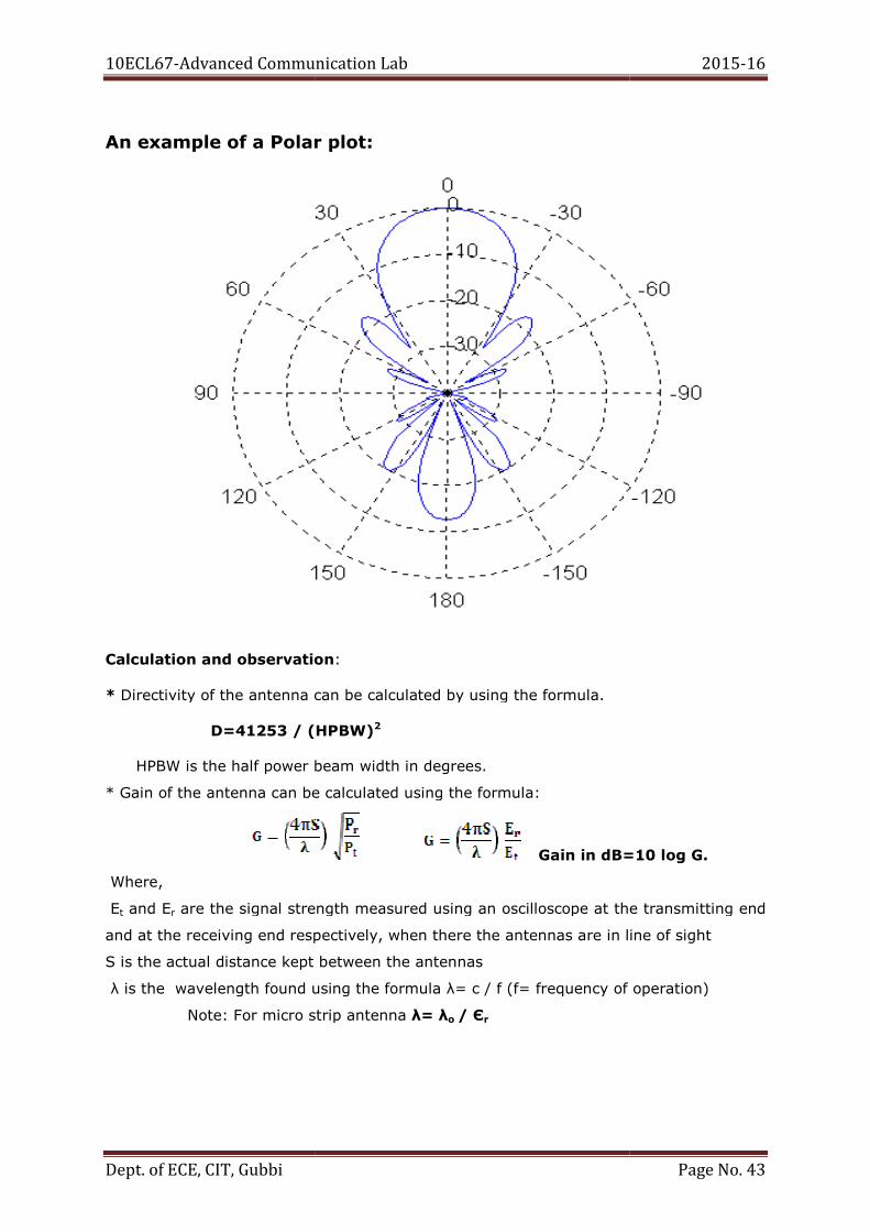
An example of a Polar plot:
Calculation and observation
* Directivity of the antenna can be calculated by using the formula.
D=41253 / (HPBW) HPBW is the half power beam width in degrees.
* Gain of the antenna can be calculated using the formula:
Where,
Et and Er are the signal strength measured using an oscilloscope at the transmitting end
and at the receiving end respectively, when there the antennas are in line of sight
S is the actual distance kept between the antennas
λ is the wavelength found using t
Note: For micro strip antenna
nced Communication Lab
An example of a Polar plot:
Calculation and observation:
Directivity of the antenna can be calculated by using the formula.
D=41253 / (HPBW)2
HPBW is the half power beam width in degrees.
* Gain of the antenna can be calculated using the formula:
Gain in dB=10 log G.
are the signal strength measured using an oscilloscope at the transmitting end
and at the receiving end respectively, when there the antennas are in line of sight
S is the actual distance kept between the antennas
λ is the wavelength found using the formula λ= c / f (f= frequency of operation)
Note: For micro strip antenna λ= λo / Єr
2015-16
Page No. 43
Gain in dB=10 log G.
are the signal strength measured using an oscilloscope at the transmitting end
and at the receiving end respectively, when there the antennas are in line of sight
he formula λ= c / f (f= frequency of operation)
10ECL67-Advanced Communication Lab 2015-16
Dept. of ECE, CIT, Gubbi Page No. 44
RESULT:
10ECL67-Advanced Communication Lab
Dept. of ECE, CIT, Gubbi
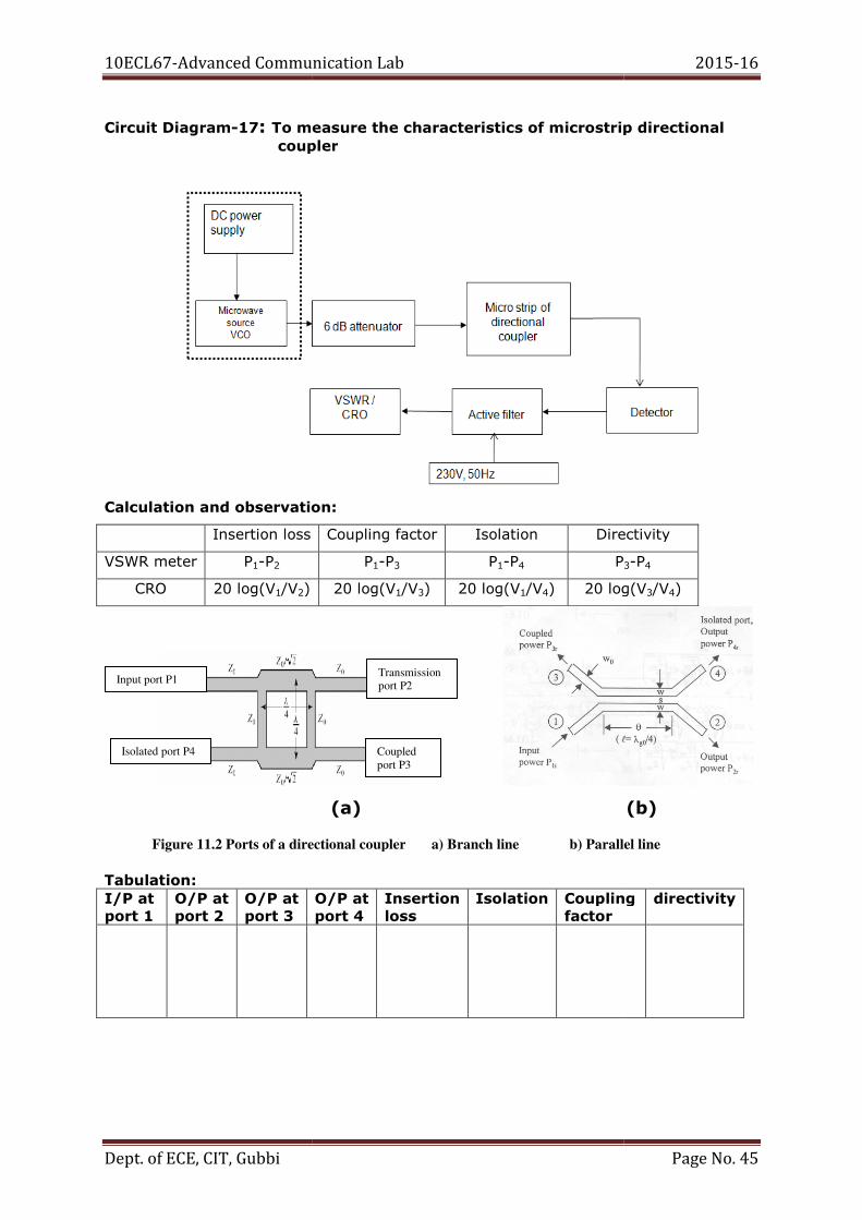
Circuit Diagram-17: To measure the characteristics of microstrip directional coupler
Calculation and observation:
Insertion loss
VSWR meter P1-P2
CRO 20 log(V1/V2)
Tabulation: I/P at port 1
O/P at port 2
O/P at port 3
Input port P1
Isolated port P4
Figure 11.2 Ports of a directional coupler
nced Communication Lab
measure the characteristics of microstrip directional coupler
Calculation and observation:
Coupling factor Isolation Directivity
P1-P3 P1-P4 P
20 log(V1/V3) 20 log(V1/V4) 20 log(V
(a)
O/P at port 4
Insertion loss
Isolation Coupling factor
Transmission
port P2
Coupled
port P3
directional coupler a) Branch line b) Parallel line
2015-16
Page No. 45
measure the characteristics of microstrip directional
Directivity
3-P4
20 log(V3/V4)
(b)
Coupling directivity
b) Parallel line
10ECL67-Advanced Communication Lab 2015-16
Dept. of ECE, CIT, Gubbi Page No. 46
Experiment No. 12 Date: __ /__ / _____
DIRECTIONAL COUPLER
Aim: To conduct an experiment to measure the coupling factor, directivity, isolation
characteristics of the directional coupler.
Components required:
Sl No Apparatus Range Quantity 1 Power supply - 1
2 transmission line 50 Ω
3 Directional
coupler 1
4 terminators 50 Ω 2
5 Oscilloscope /
VSWR meter - 1
Procedure:
1. Set up the system as shown in circuit diagram-17.
2. Keeping the voltage at minimum, switch on the power supply.
3. Insert a 50 Ω transmission line and check for the output at the end of the system
using a CRO/ VSWR meter.
4. Vary the power supply voltage and check the output for different VCO
frequencies.
5. Note down the output for different output frequencies.
6. Replace the 50 Ω transmission line with branch line coupler.
7. Check the output at port 2(throughput), 3(Coupled output), 4(isolated output).
8. Calculate insertion loss, coupling factor and isolation using the formulae given.
Note: The coupled and Isolated ports of branch line Directional Coupler are
respectively Isolated and Coupled ports in Parallel line Directional Coupler
Result:
10ECL67-Advanced Communication Lab
Dept. of ECE, CIT, Gubbi
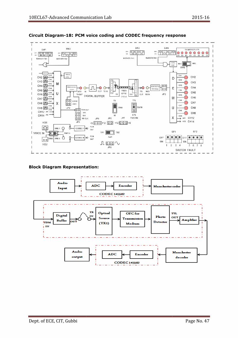
Circuit Diagram-18: PCM voice coding and
Block Diagram Representation:
nced Communication Lab
PCM voice coding and CODEC frequency response
Block Diagram Representation:
2015-16
Page No. 47
CODEC frequency response
10ECL67-Advanced Communication Lab 2015-16
Dept. of ECE, CIT, Gubbi Page No. 48
Experiment No. 13 Date: __ /__ / _____
PCM generation and detection using a CODEC Chip
Aim: To study the liberalized a law PCM coding, analog to digital conversion, the reverse
process and the filtering characteristics of the CODEC chip 145502.
Components required:
Sl No Apparatus Range Quantity 1 Power supply - 1
2 Link B Kit - 1
3 Patch cords -
4 Function
generator 1MHz 1
5 Dual Trace
Oscilloscope
20MHz
1
Procedure:
1. Make the connections as shown in circuit diagram-18. Connect the power supply
cables with proper polarity to Link B kit. While connecting this, ensure that the
power supply is OFF.
2. Now voice communication can be done between the audio channels using
telephone headset.
3. Observe the effect on the voice signal at various test points.
4. Keep the switch SW6 towards SINE IN position.
5. Feed a sinusoidal signal of 1KHz and the amplitude up to 2Vpp to SINE 1 and
SINE 2 input terminals. This gives an analog input to both the CODECs.
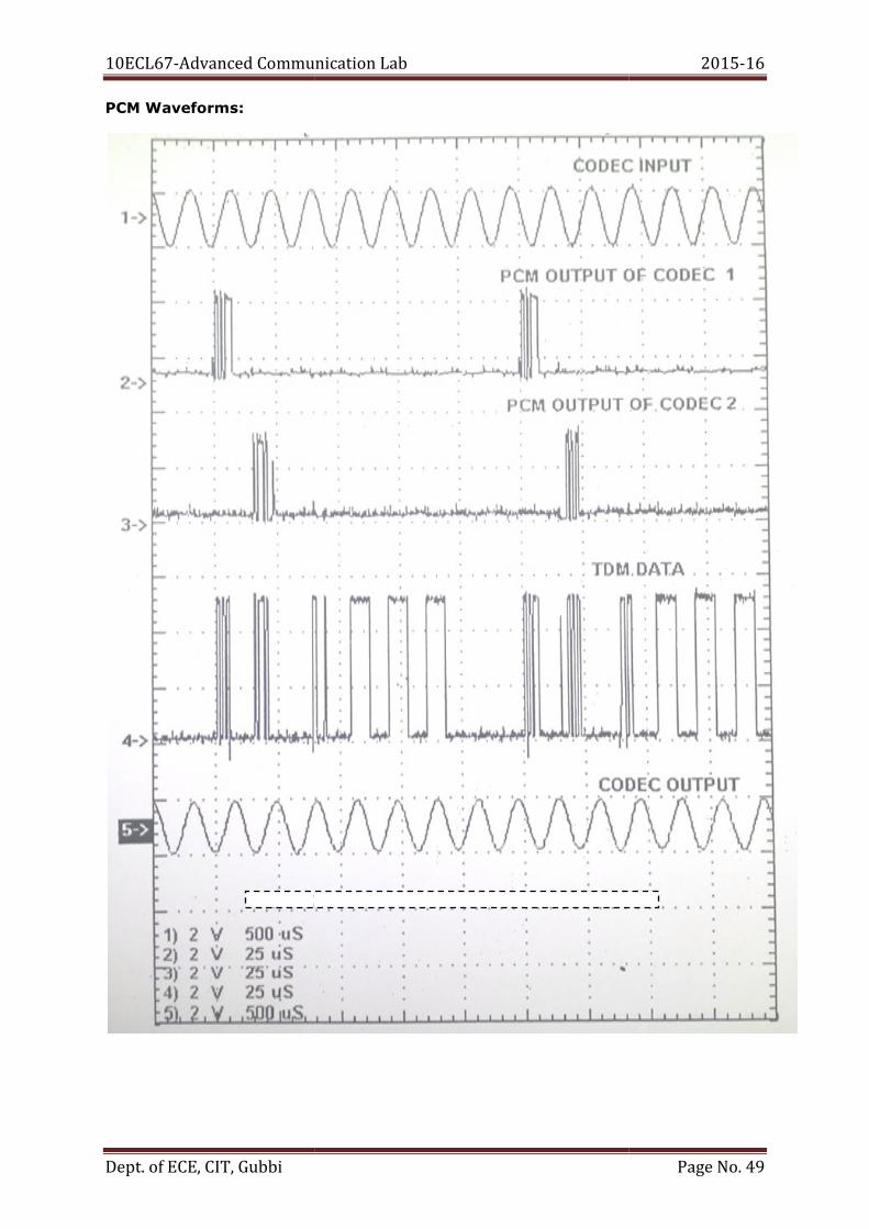
6. Observe the reconstructed waveform at OUT post of CODEC 1 RX and at OUT post
for CODEC II RX as shown PCM waveform. Compare both the applied input and
the reconstructed signal on the oscilloscope.
7. Observe the signal changes at various test points.
8. Vary the input signal frequency in steps and simultaneously observe the output
signal. Measure the amplitude of the output signal for each input frequency.
9. Find the frequency reading after which the response of the codec drops. This
gives the bandwidth of the codec.
10. Since it works for audio range we should get bandwidth around 3.4KHz.
SWITCH and Jumper Connections Keep all switch faults in OFF position.
Keep switch SW6 towards SINE IN position.
Keep switch SW8 towards TX position.
Keep Switch SW9 towards TX1 position.
Keep Switch SW10 towards TTL position.
Keep Jumper JP1 at TDM OUT position.
Keep Jumper JP2 at 1.024M position.
Keep Jumper JP5 towards +5V position.
Keep Jumper JP6 shorted.
Keep Jumper JP8 towards Pulse position.
10ECL67-Advanced Communication Lab
Dept. of ECE, CIT, Gubbi
PCM Waveforms:
nced Communication Lab
2015-16
Page No. 49
10ECL67-Advanced Communication Lab 2015-16
Dept. of ECE, CIT, Gubbi Page No. 50
Result:
10ECL67-Advanced Communication Lab 2015-16
Dept. of ECE, CIT, Gubbi Page No. 51
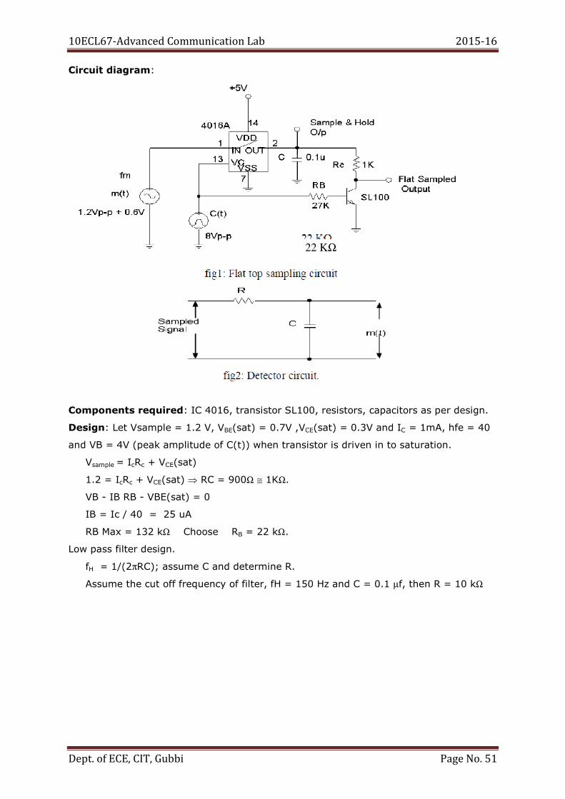
Circuit diagram:
Components required: IC 4016, transistor SL100, resistors, capacitors as per design.
Design: Let Vsample = 1.2 V, VBE(sat) = 0.7V ,VCE(sat) = 0.3V and IC = 1mA, hfe = 40
and VB = 4V (peak amplitude of C(t)) when transistor is driven in to saturation.
Vsample = IcRc + VCE(sat)
1.2 = IcRc + VCE(sat) ⇒ RC = 900Ω ≅ 1KΩ.
VB - IB RB - VBE(sat) = 0
IB = Ic / 40 = 25 uA
RB Max = 132 kΩ Choose RB = 22 kΩ.
Low pass filter design.
fH = 1/(2πRC); assume C and determine R.
Assume the cut off frequency of filter, fH = 150 Hz and C = 0.1 µf, then R = 10 kΩ
22 KΩ
10ECL67-Advanced Communication Lab 2015-16
Dept. of ECE, CIT, Gubbi Page No. 52
Additional Experiment 1:
Verification of Sampling Theorem using Flat Top Samples
Aim: To design a circuit for generating flat top samples and to verify Sampling theorem.
Procedure:
1. Rig up the circuit as shown in circuit diagram.
2. Apply a low frequency sine wave as the message signal say 100Hz (Apply dc
offset).
3. Apply a high frequency square wave as the carrier signal.
4. Without connecting the capacitor observe the output at pin no 2, the samples are
naturally sampled.
5. Now check the output for different cases by applying the signals at different
frequencies and verify the Nyquist rate.
6. Now connect the capacitor in the circuit and get the sample and hold samples and
flat top sampled output.
7. Connect the sampled output as a input to the demodulator input and reconstruct
the original message signal.
10ECL67-Advanced Communication Lab 2015-16
Dept. of ECE, CIT, Gubbi Page No. 53
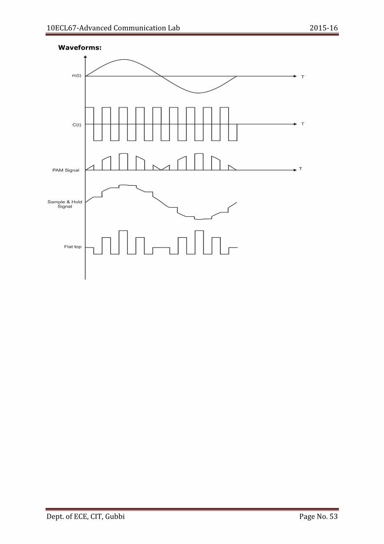
Waveforms:
10ECL67-Advanced Communication Lab 2015-16
Dept. of ECE, CIT, Gubbi Page No. 54
Result:
10ECL67-Advanced Communication Lab 2015-16
Dept. of ECE, CIT, Gubbi Page No. 55
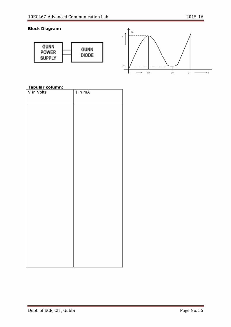
Block Diagram:
Tabular column: V in Volts I in mA
10ECL67-Advanced Communication Lab 2015-16
Dept. of ECE, CIT, Gubbi Page No. 56
Additional Experiment 2:
GUNN DIODE
Aim: To Conduct an experiment to obtain V-I characteristics of GUNN Diode. Theory:
The gunn oscillator is based on negative differential conductivity effecting bulk
semiconductors which has two conduction bands separated by energy gap (greater than
thermal energies). A disturbance at the cathode gives rise to high field region which
travels towards the anode. When this field domain reaches the anode, it disappears and
another domain is formed at the cathode and starts moving towards anode and so on.
The time required for domain to travel form cathode to anode (transit time) gives
oscillation frequency. In the gunn oscillator, the gunn diode is placed in a resonant
cavity. The oscillation frequency is determined by cavity dimensions.
Although gunn oscillator can be amplitude modulated with the bias voltage. We
have used a PIN modulator for square wave modulation of the signal coming from gunn
diode.
A measure of the square wave modulation capability is the modulation depth
i.e., the output ratio between the ON and OFF state.
Procedure:
To find V-I Characteristics of GUNN diode:
1) Set up the microwave bench as shown in block diagram 1.
2) Connect only the GUNN bias signal to the GUNN diode.
3) Witch GUNN bias voltage to minimum position switch ON the power supply.
4) Increase the bias voltage in steps of 1 volt and note down the voltage and
current by alternatively switching the indicator from V to I . Each time note the
value of V and I.
Note: [Up to the threshold voltage current increases with increase in voltage (+ve
resistance) and after threshold current decreases with increase in voltage (-ve
resistance)]
Result :
10ECL67-Advanced Communication Lab 2015-16
Dept. of ECE, CIT, Gubbi Page No. 57
Sample Viva questions
1. State the difference between Analog systems and digital systems.
2. Explain why digital systems are considered superior to Analog systems.
3. Mention the disadvantages of Analog communication.
4. Explain the basic steps involved in digitizing a signal.
5. Explain ASK operation.
6. State the difference between discrete and digital signals.
7. Define Quantizing.
8. Define Encoding.
9. Explain PCM encoding.
10. State the difference between pulse modulation and digital modulation.
11. Explain FSK circuit operation.
12. Explain different types of channels.
13. Mention the basic blocks of formatting and transmission of base band signals.
14. Mention the difference between broad band transmission and base band
transmission.
15. Explain PSK operation.
16. Define VSWR.
17. Define Characteristics impedance.
18. Define a Wave guide.
19. Give the S-Matrix for an ideal waveguide.
20. What is TDM?
21. What is FDM?
22. Compare TDM and FDM.
23. What are the applications of TDM?
24. What is an optical fiber? What are its advantages?
25. Explain the principle of total internal reflection
26. What is meant by numerical aperture?
27. What is a ring resonator?
28. Define the following: Isolation, Coupling factor, and Insertion loss.
29. Mention the range of microwave frequencies.
30. Explain the operation of a reflex klystron.
10ECL67-Advanced Communication Lab 2015-16
Dept. of ECE, CIT, Gubbi Page No. 58
References
1. Simon Haykin, “Digital Communications”, John Wiley & Sons, 2008.
2. K. N. Hari Bhat and D. Ganesh Rao, “Digital Communications”, Pearson , 3rd
edition.
3. K. Sam Shanmugam, “An introduction to Analog and Digital Communication”,
John Wiley India Pvt. Ltd, 2008.
4. John D. Krauss, “Antennas and Wave Propagation, 4th Edition, McGraw-Hill
International edition, 2010.
5. Annapurna Das, Sisir K. Das, “ Microwave Engineering”, Tata McGraw-Hill
Education, 2nd edition, 2000
10ECL67-Advanced Communication Lab 2015-16
Dept. of ECE, CIT, Gubbi Page No. 59
Question Bank
1. Design and simulate an ASK system to transmit digital data using a suitable carrier.
Demodulate the ASK signal with the help of suitable circuit. Determine the minimum
frequency of carrier for proper detection.
2. Design and simulate the working of FSK with a suitable circuit for _____ Hz and __
Hz carrier signals. Demodulate the FSK signal with the help of suitable circuit.
3. Design and simulate the working of BPSK modulated signal for a given carrier signal
of ______ Hz. Demodulate the BPSK signal to recover the digital data.
4. Design and simulate the working of TDM for PAM signals with _____ Hz and _____
Hz message signals. Also demultiplex the message signals.
5. Conduct a suitable experiment using slotted line carriage to obtain the following for
the given load. a) λg and λo b) VSWR
6. Conduct a suitable experiment using fiber optic trainer kit to determine the numerical
aperture of the optical fiber.
7. Conduct a suitable experiment using fiber optic trainer kit to determine:
a) Attenuation b) Bending loss
8. With the help of suitable circuit demonstrate the working of DPSK encoder and
Decoder for the specified input stream and carrier frequency simulate the same in
software.
9. With the help of a suitable circuit demonstrate the working of QPSK modulator and
demodulator.
10. Conduct an experiment using fiber optic trainer kit to establish analog link with TDM.
11. Conduct an experiment using fiber optic trainer kit to establish digital link and
measure the following: a) Attenuation, b) Bending loss and c) Numerical aperture.
12. Conduct an experiment to obtain the radiation pattern of micro strip patch antenna.
Also calculate the directivity and gain of the antenna.
13. Conduct an experiment to obtain radiation pattern of micro strip dipole antenna. Also
calculate the directivity and gain of the antenna.
10ECL67-Advanced Communication Lab 2015-16
Dept. of ECE, CIT, Gubbi Page No. 60
14. Conduct an experiment to obtain radiation pattern of micro strip yagi antenna. Also
calculate the directivity and gain of the antenna.
15. Conduct an experiment on a given micro strip directional coupler to determine the
following: a) Isolation b) Coupling factor c) Insertion Loss
16. Conduct an experiment on a given micro strip power divider to determine the
following: a) Isolation b) Coupling factor
17. Conduct an experiment to find the characteristics of micro strip ring resonator. Also
calculate the dielectric constant of the given dielectric material.
18. Conduct an experiment using fiber optic trainer kit to establish digital link for the
realization of PCM technique.
APPENDIX
Introduction to LabVIEW
LabVIEW (Laboratory Virtual Instrument Engineering Workbench) is a system-design
platform and development environment for a visual programming
language from National Instruments. Originally released for the Apple Macintosh in 1986,
LabVIEW is commonly used for data acquisition, instrument control, and industrial
automation on a variety of platforms including Microsoft Windows, various versions
of UNIX, Linux and Mac OS X. The latest version of LabVIEW is LabVIEW 2014.
Like C, JAVA, the LabVIEW software is known as ‘G’ language. Its interfacing is GUI
(Graphical User Interfacing) i.e. the complete program is represented in block diagrams
instead of having syntaxes.
Benefits
1. Interfacing to Devices
A key feature of LabVIEW is the extensive support for interfacing to devices such
as instruments, cameras, and other devices. Users can interface hardware by
either writing direct bus commands (USB, GPIB, Serial...) or using high-level,
device-specific drivers that provide native LabVIEW function nodes for controlling
the device.
2. Code Compilation
In terms of performance, LabVIEW includes a compiler that produces native code
for the CPU platform. The graphical code is translated into executable machine
code by interpreting the syntax and by compilation.
3. Large Libraries
Many libraries with a large number of functions for data acquisition, signal
generation, mathematics, statistics, signal conditioning, analysis, etc., along with
numerous graphical interface elements are provided in several LabVIEW package
options. The number of advanced mathematic blocks for functions such as
integration, filters, and other specialized capabilities usually associated with data
capture from hardware sensors is immense.
4. Code re-use
The fully modular character of LabVIEW code allows code reuse without
modifications: as long as the data types of input and output are consistent so
they are interchangeable.
5. Parallel Programming
LabVIEW is an inherently concurrent language, so it is very easy to program
multiple tasks that are performed in parallel by means of multithreading. This is,
for instance, easily done by drawing two or more parallel while loops.
FUNCTIONS IN LabVIEW
1. Acquiring Data and Processing Signals
Measure any sensor on any bus
Perform advanced analysis and signal processing
Display data on custom user interfaces
Log data and generate reports
2. Instrument Control
Automate data collection
Control multiple instruments
Analyze and display signals
3. Automating Test and Validation Systems
Automate the validation or manufacturing test of your product
Control multiple instruments
Analyze and display test results with custom user interfaces
4. Embedded Monitoring and Control Systems
Reuse ANSI C and HDL code
Integrate off-the-shelf hardware
Prototype with FPGA technology
Access specialized tools for medical, robotics, and more
5. Academic Teaching
Apply an interactive, hands-on approach to learning
Combine algorithm design with real-world data measurements
Increase application performance with multicore processing
6. Prototyping
SDR algorithm prototyping
LTE and 802.11 development frameworks
Single design environment for FPGAs
Steps to Create VI in LabVIEW
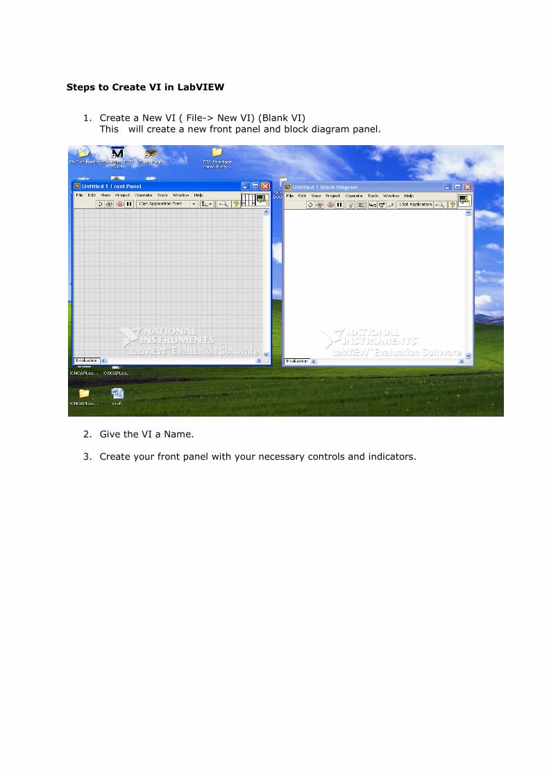
1. Create a New VI ( File-> New VI) (Blank VI)
This will create a new front panel and block diagram panel.
2. Give the VI a Name.
3. Create your front panel with your necessary controls and indicators.
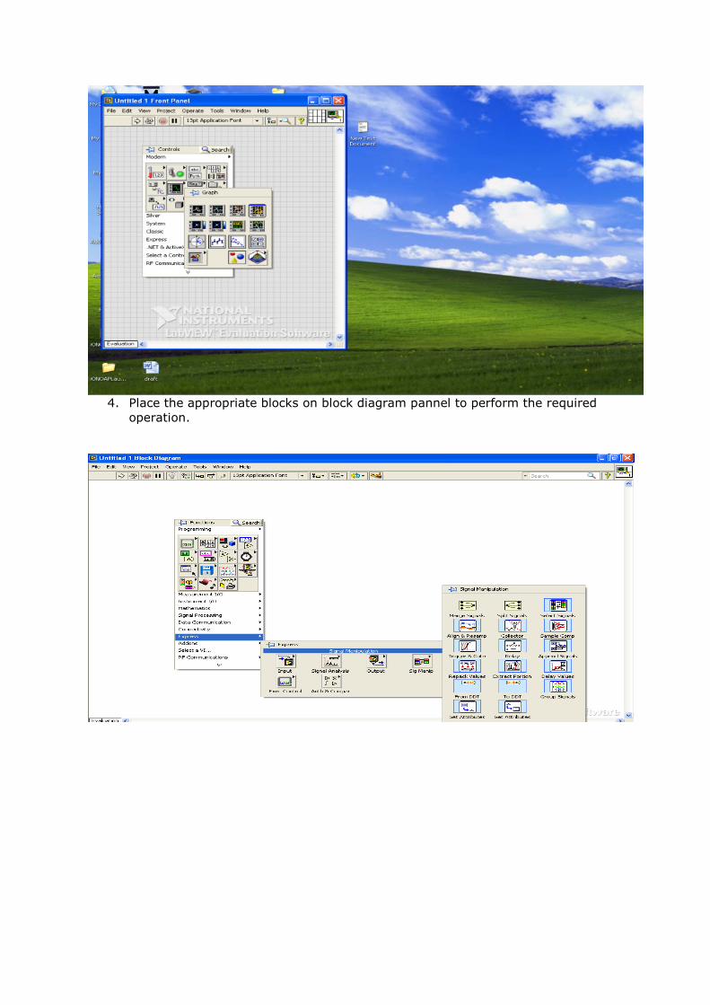
4. Place the appropriate blocks on block diagram pannel to perform the required
operation.
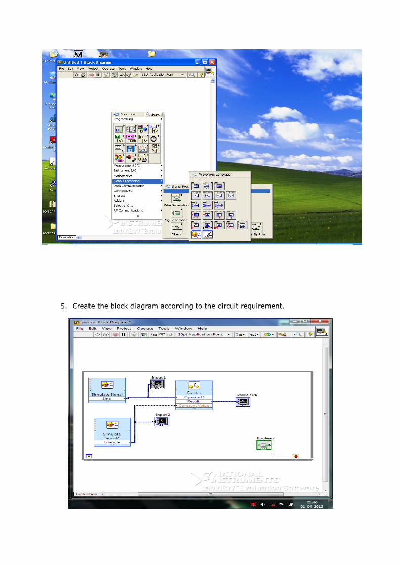
5. Create the block diagram according to the circuit requirement.
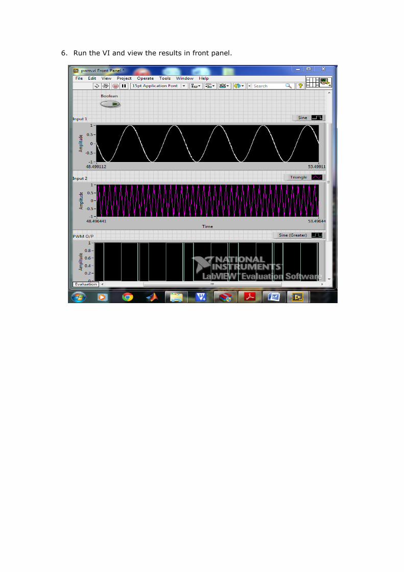
6. Run the VI and view the results in front panel.