a new general topology for cascaded multilevel inverters ... · volume 4, issue 4 july 2015 ijraet...
TRANSCRIPT

Volume 4, Issue 4 JULY 2015
IJRAET
A New General Topology For Cascaded Multilevel Inverters With Reduced Number Of Components Based
On Developed H-Bridge
MOIRANGTHEM SAMSON JNTUH, Hyderabad
E-Mail Id: [email protected]
Mr. MOHAMMED SALEEM JNTUH, Hyderabad
E-mail Id : [email protected]
ABSTRACT -In this paper, a new general cascaded multilevel inverter using developed H-bridges is proposed. The proposed topology requires a lesser number of dc voltage sources and power switches and consists of lower blocking voltage on switches, which results in decreased complexity and total cost of the inverter. These abilities obtained within comparing the proposed topology with the conventional topologies from aforementioned points of view. Moreover, a new algorithm to determine the magnitude of dc voltage sources is proposed. The performance and functional accuracy of the proposed topology using the new algorithm in generating all voltage levels for a 31-level inverter are confirmed by simulation . Also a slightly different topology with 49 level inverter is presented. The difference between the 49 level inverter and the other topology presented in this paper is that without increasing the number of voltage sources the number of levels is increased by increasing the number of switches. The 49 level inverter will be simulated
Index Terms— voltage source inverter, developed H-bridge, multilevel inverter, Cascaded multilevel inverter.
I. INTRODUCTION
With the advancement in inverters, multilevel inverters have received more attention because high-power and medium voltage ratings provides advantage in of high power quality, lower order harmonics, and better electromagnetic interference etc. By appropriately arranging the semi-conductor based switches the inverter will generate a stepped voltage waveform. The main structures of the multilevel inverters have been presented: “diode clamped multilevel inverter”, “flying capacitor multilevel inverter,” and “cascaded multilevel inverter”. Multilevel inverters is composed of
symmetric and asymmetric groups based on the dc voltage sources. The cascaded multilevel inverter is composed of a number of single-phase H-bridge inverters and is classified into symmetric and asymmetric groups based on the magnitude of dc voltage sources. In the symmetric types, the magnitudes of the dc voltage sources of all H-bridges are equal while in the asymmetric types, the values of the dc voltage sources of all H-bridges are different. In recent years, several topologies with various control techniques have been presented for cascaded multilevel inverters [5]–[8]. In [4] and [9]–[15], different symmetric cascaded multilevel inverters have been presented. The main advantage of all these structures is the low variety of dc voltage sources, which is one of the most important features in determining the cost of the inverter. On the other hand, because some of them use a high number of bidirectional power switches, a high number of insulated gate bipolar transistors (IGBTs) are required, which is the main disadvantage of these topologies. An asymmetric topology has been presented in [16]. The main disadvantage of this structure is related to its bidirectional power switches, which cause an increase in the number of IGBTs and the total cost of the inverter. In [15], a new topology with three algorithms have been presented, which reduce the number of required power switches but increase the variety of dc voltage sources. In [1], [4] and [17], and [18], several algorithms for determining the magnitudes of dc voltage sources for the conventional cascaded multilevel inverter have been presented. The major advantage of this topology and its algorithms is related to its ability to generate a considerable number of output voltage levels by using a low number of dc voltage sources and power switches but the high variety in the magnitude of dc voltage sources is their most remarkable disadvantage. In this paper, in order to increase the number of output

Volume 4, Issue 4 JULY 2015
IJRAET
voltage levels and reduce the number of power switches, driver circuits, and the total cost of the inverter, a new topology of cascaded multilevel inverters is proposed. It is important to note that in the proposed topology, the unidirectional power switches are used. Then, to determine the magnitude of the dc voltage sources, a new algorithm is proposed. Moreover, the proposed topology is compared with other topologies from different points of view such as the number of IGBTs, number of dc voltage sources, the variety of the values of the dc voltage sources, and the value of the blocking voltages per switch. Finally, the performance of the proposed topology in generating all voltage levels through a 49 -level inverter is confirmed by MATLAB simulation.
II. PROPOSEDTOPOLOGY
In Fig. 1, two new topologies are proposed for a seven-level inverter [19]. As shown in Fig. 1, the proposed topologies are obtained by adding two unidirectional power switches and one dc voltage source to the H-bridge inverter structure. In other words, the proposed inverters are comprised of six unidirectional power switches (푆 , 푆 , 푆 , , 푆 , ,푆 , , 푎푛푑 푆 , ) and two dc voltage sources (푉 , 푎푛푑푉 , ). In this paper, these topologies are called developed H-bridge. As shown in Fig. 1, the simultaneous turn-on of 푆 , 푎푛푑 푆 , (표푟 푆 , 푎푛푑 푆 , )
Fig. 1. Proposed seven-level inverters. (a) First proposed topology. (b) Second proposed topology. No. 푆 , 푆 , 푆 , 푆 , 푆 푆 푣 (퐹푖푔 .1(푎)) 푣 (퐹푖푔 .1(푏))
1 1 0 0 1 0 1 푉 , 푉 , 2 1 0 0 1 1 0 푉 , −푉 , 3 1 0 1 0 0 1 푉 , − 푉 , 푉 , + 푉 ,
4 1 0 1 0 1 0 0 0 0 1 0 1 0 1
5 0 1 1 0 1 0 −푉 , −푉 , 6 0 1 1 0 0 1 −푉 , 푉 , 7 0 1 0 1 1 0 -(푉 , − 푉 , ) -(푉 , + 푉 , )
causes the voltage sources to short-circuit. Therefore, the simultaneous turn-on of the mentioned switches must be avoided. In addition, 푆 and 푆 should not turn on, simultaneously. The difference in the topologies illustrated in Fig. 1 is in the connection of the dc voltage sources polarity. Table I shows the output voltages of the proposed inverters for different states of the switches. In this table, 1 and 0 indicate the 푂푁 − and 푂퐹퐹 − states of the switches, respectively. As it is obvious from Table I, if the values of the dc voltage sources are equal, the number of voltage levels decreases to three. Therefore, the values of dc voltage sources should be different to generate more voltage levels without increasing the number of switches and dc voltage sources. Considering Table I, to generate all voltage levels (odd and even) in the proposed topology shown in Fig. 1(a), the magnitudes of 푉 , and 푉 , should be considered 3푝푢 and 1푝푢, respectively. Similarly, for the topology shown in Fig. 1(a), the magnitudes of 푉 , and 푉 , should be considered 2푝푢 and 1푝푢, respectively. Considering the aforementioned explanations, the total cost of the proposed topology in Fig. 1(b) is low because dc voltage sources with low magnitudes are needed. By developing the seven-level inverter shown in Fig. 1(b), the 31-level inverter shown in Fig. 2 can be proposed. This topology consists of ten unidirectional power switches and four dc voltage sources. According to Fig. 2, if the power switches of (푆 , ,푆 , ), (푆 , ,푆 , ), (푆 , ,푆 , ), and (푆 , ,푆 , ) turn on simultaneously, the dc voltage sources of푉 , ,푉 , ,푉 , , and 푉 , will be short-circuited, respectively. Therefore, the simultaneous turn-on of these switches should be avoided. In addition, 푆 and 푆 should not turn on simultaneously. It is important to note that the 31-level topology can be provided through the structure presented in Fig. 1(a), where the only difference will be in the polarity of the applied dc voltage sources. By developing the proposed 31 level inverter, a 127 -level inverter can be proposed as shown in Fig. 3. This topology

Volume 4, Issue 4 JULY 2015
IJRAET
Fig. 3. Proposed 127-level inverter.
Fig. 4. Proposed general topology. consists of 14 unidirectional power switches and 6 dc voltage sources. Similarly, by developing the proposed basic topology, a general topology, as shown in Fig. 4, can be proposed. The general topology consists of 2푛 dc voltage sources (푛 is the number of the dc voltage sources on each leg) and 4푛 + 2 unidirectional power switches. In the proposed general topology, the number of output voltage levels(푁 ), number of switches (푁 ), number of dc voltage sources(푁 ), and the
maximum magnitude of the generated voltage (푉 , ) are calculated as follows, respectively:
푁 = 2 − 1 ------------ (1)
푁 = 4푛 + 2 ----------- (2)
푁 = 2푛 ------------ (3)
푉 , = 푉 , + 푉 , ------------- (4)
The other important parameters of the total cost of a multilevel inverter for evaluation are the variety of the values of dc voltage sources and the value of the blocking voltage of the switches. As the variety of dc voltage sources and the value of the blocking voltage of the switches are low, the inverter’s total cost decreases [20]. The number of variety of the values of dc voltage sources 푁 is given by
푁 = 2푛 ----------- (5)
The following pattern is utilized to calculate the maximum magnitude of the blocking voltage of the power switches. As shown in Fig. 1(b), the blocking voltage of 푆 , and 푆 , are calculated as follows:
푉 , = 푉 , = 푉 , ----------- (6)
Where 푉 , and 푉 , indicate the maximum blocking voltages of 푆 , and 푆 , , respectively. The blocking voltage of 푆 , and 푆 , are as follows:
푉 , = 푉 , = 푉 ,
----------- (7) Where 푉 , and 푉 , indicate the maximum blocking voltages of 푆 , and 푆 , , respectively. Therefore, the maximum blocking voltage of all switches in the proposed seven-level inverter (푉 , )is calculated as follows: 푉 , = 푉 , + 푉 , + 푉 , + 푉 , + 푉 + 푉
= 4(푉 , + 푉 , ) ----------- (8)
Considering Fig. 2, the maximum blocking voltage of the switches is as follows:
푉 , = 푉 , = 푉 , ------------ (9)
푉 , = 푉 , = 푉 , − 푉 , ----------- (10)
푉 , = 푉 , = 푉 , --------------- (11)
푉 , = 푉 , = 푉 , − 푉 , ---------------(12)
푉 = 푉 = 푉 , + 푉 , ------- (13)

Volume 4, Issue 4 JULY 2015
IJRAET
Therefore, the maximum blocking voltage of all switches of the proposed 31-level inverter(푉 , )is as follows: 푉 , = 푉 , + 푉 , + 푉 , + 푉 , + 푉 ,
+ 푉 , + 푉 , + 푉 , + 푉 + 푉= 4(푉 , + 푉 , )
--------- (14) Similarly, the maximum blocking voltage of all switches of the 49-level inverter is calculated as follows:
푉 , = 4(푉 , + 푉 , ) ----------- (15)
Finally, the maximum blocking voltage of all the switches of the general topology 푉 , is calculated as follows:
푉 , = 4(푉 , + 푉 , ) ------------ (16)
III. PROPOSED ALGORITHM TO DETERMINE
THE MAGNITUDES OF DC VOLTAGE SOURCES
In this paper, the following algorithm is applied to determine the magnitude of dc voltage sources. It is important to note that all voltage levels (even and odd) can be generated.
A. Proposed Seven-Level Inverter
The magnitudes of the dc voltage sources of the seven-level inverter shown in Fig. 1(b) are determined as follows: VL,1 =Vdc (17) VR,1 =2Vdc. (18) Considering (17), (18), and Table I, the proposed seven-level inverter can generate 0, ±Vdc, ±2Vdc, and ±3Vdc at output .
B. Proposed 31-Level Inverter
The magnitudes of the dc voltage sources of the proposed 31-level inverter are recommended as follows: VL,1 =Vdc (19) VR,1 =2Vdc (20) VL,2 =5Vdc (21) VR,2 =10Vdc. (22) The proposed inverter can generate all negative and positive voltage levels from 0 to 15Vdc with steps of Vdc.
C. Proposed 127-Level Inverter
The magnitudes of the dc voltage sources of the proposed 127-level inverter are calculated as follows:
푉 , = 푉 ----------- (17)
푉 , = 2푉 ----------- (18)
푉 , = 5푉 ----------- (19)
푉 , = 10푉 ----------- (20)
푉 , = 25푉 ---------- (21)
푉 , = 50푉 ---------- (22)
By using this algorithm, the inverter can generate all negative and positive voltage levels from 0 to 63 푉 with steps of 푉 D. Proposed General Multilevel Inverter The magnitudes of the dc voltage sources of the proposed general multilevel inverter can be obtained as follows:
푉 = 5 푉 푓표푟 푗 = 1,2,3, … . ,푛 --------- (23)
푉 = 2 × 5 푉 푓표푟 푗 = 1,2,3, … . , 푛 ------------- (24)
Considering (4) and (16), the values of 푉 , and 푉 , of the proposed general multilevel inverter are as follows, respectively:
푉 , = 푉 , + 푉 , = 3 × 5 푉 ---------- (25)
푉 , = 4 푉 , + 푉 , = 12(5 )푉 ----------- (26)
IV. CALCULATION OF LOSSES
Mainly, two kinds of losses (i.e., conduction and switching losses) are associated with the switches. Since the switches include IGBTs and diodes, the conduction losses of an IGBT (푝 , (푡)) and a diode (푝 , (푡)) are calculated as follows, respectively [7], [22]:
푝 , (푡) = 푉 + 푅 푖 (푡) 푖(푡) ----------- (27)
푝 , (푡) = 푉 + 푅 푖 (푡) 푖(푡) ------------ (28)
Where 푉 and 푉 are the forward voltage drops of the IGBT and diode, respectively. 푅 and 푅 are the equivalent resistances of the IGBT and diode, respectively, and 훽 is a constant related to the specification of the IGBT. Considering that at instant 푡, there are 푁 transistors and 푁 diodes in the current path, the average value of the conduction

Volume 4, Issue 4 JULY 2015
IJRAET
power loss (푃 ) of the multilevel inverter can be written as follows:
푃 =12 [푁 (푡)푝 , (푡) + 푁 (푡)푝 , (푡)] 푑푡
------------ (29) The switching losses are calculated based on the energy loss calculation. The switching losses occur during the turn-off and turn-on periods. For simplicity, the linear variations of the voltage and current of the switches in the switching period are considered. Based on this assumption, the following relations can be written [7], [22]:
퐸 , = 푣(푡)푖(푡)푑푡 =16푉 , 퐼푡
---------- (28)
퐸 , = 푣(푡)푖(푡)푑푡 =16푉 , 퐼 푡
---------- (29) Where 퐸 , and 퐸 , are the turn-off and turn-on losses of the switch 푘, respectively.푡 and 푡 are the turn-off and turn-on times of the switch, respectively,퐼 is the current through the switch before turning off, 퐼 is the current through the switch after turning on, and 푉 , is the OFF-state voltage on the switch. The switching power loss (푃 ) is equal to the sum of all turn-on and turn-off energy losses in a fundamental cycle of the output voltage. This can be written as follows [7], [22]:
푃 = 푓 퐸 , + 퐸 ,
,,
----------- (30) Where 푓 is the fundamental frequency and 푁 , and 푁 , are the numbers of turn-on and turn-off of the switch 푘 during a fundamental cycle. Also, 퐸 , is the energy loss of the switch 푘 during the 푖푡ℎ turn-on and 퐸 , is the energy loss of the switch 푘 during the 푖푡ℎ turn-off. The total loss(푃 )of the multilevel converter is the sum of the conduction and switching losses as follows:
푃 = 푃 + 푃 -------- (31)
Finally, the efficiency (휂) of the inverter is calculated as follows:
휂 =푃푃 =
푃푃 + 푃
---------- (32) Where 푃 and 푃 denote the output and input powers of the inverter.
V. COMPARING THE PROPOSED GENERAL TOPOLOGY WITH THE CONVENTIONAL
TOPOLOGIES
In order to clarify the advantages and disadvantage of the proposed topology, it should be compared with the different kinds of topologies presented in literature. In [4], the conventional cascaded multilevel inverter with two different algorithms has been presented. These algorithms are known as the symmetric cascaded multilevel inverters and the asymmetric ones with the binary method for determining the magnitude of dc voltage sources. In the comparison, the conventional symmetric cascaded multilevel inverter is indicated by 푅 and the conventional binary asymmetric cascaded multilevel inverter is shown by 푅 . Three other algorithms have been presented for this topology in [1], [17], and [18], which are indicated by 푅 –푅 , respectively. Moreover, another topology with three different algorithms for determining the value of dc voltage sources has been introduced in [15], which are shown by 푅 –푅 in this comparison. In [9]–[12], four different structures for the cascaded multilevel inverter have been presented, and in this paper, they are indicated by 푅 –푅 and 푅 –푅 . It is important to note that the power switches in the aforementioned topologies are unidirectional. In addition, other topologies based on bidirectional switches have been presented in [13] and [14]. In [14], three different algorithms have been recommended, which are denoted as푅 –푅 , and the presented topology in [13] is indicated by 푅 in this comparison. Fig. 5 shows all of the aforementioned structures. Fig. 6 compares the number of IGBTs of the proposed general topology with the aforementioned cascaded multilevel inverters. It is obvious that the proposed inverter requires a lesser number of IGBTs in comparison with the other mentioned topologies to generate particular levels. Fig. 7 compares the number of dc voltage sources of the proposed inverter with the aforementioned cascaded multilevel inverter. As shown in Fig. 7, the proposed inverter has better performance in comparison with the other presented topologies except the topology presented in 푅 . However, the magnitude of the dc voltage sources in 푅 is a little more than that of the proposed topology. Fig. 8 compares the variety of magnitudes of the dc voltage sources of the proposed inverter with that of the aforementioned cascaded multilevel inverter. Obviously, the proposed inverter uses a wider variety of magnitudes of the dc voltage sources in comparison with those of all the aforementioned

Volume 4, Issue 4 JULY 2015
IJRAET
topologies. This feature is the most important disadvantage of the proposed topology because the variety of the values of dc voltage sources is as one of the remarkable factors in determining the cost of the inverter. However, this feature in the proposed topology is similar to the presented topologies of 푅 and 푅 . Fig. 9 compares the magnitude of the blocking voltage of the switches of the proposed inverter with that of the aforementioned cascaded multilevel inverter. This figure shows the reduction
of the magnitude of the blocking voltage of the proposed inverter in comparison with those of all the aforementioned multilevel inverters.
Fig. 5. Cascaded multilevel inverters presented in literature: (a) Conventional cascaded multilevel inverters R1 for V1 = V2 = · · · = Vn = Vdc, R2 for V1 = 2j−1Vdc (j = 1, 2, . . . , n), R3 for V1 = 3j−1Vdc (j = 1, 2, . . . , n), R4 for V1 = 0.5V2 = 0.5V3 = · · · = 0.5Vn = Vdc, and R5 for V1 = 2/3 =V3/3 = · · · = Vn/3 = Vdc. (b) Presented topology in [12], namely, R12 for V1 = V2 = · · · = Vn = Vdc. (c) Presented topology in [10], i.e., R7 for V1 = V2 = · · · = Vn = Vdc. (d) Presented topology in [9], i.e., R6 for V1 = V2 = · · · = Vn = Vdc. (e) Presented topologies in [14], i.e., R8 for V1 = V2 · · · = Vn = Vdc, R9 for V1 = 0.5V2 = 0.5V3 = · · · = 0.5Vn = Vdc, and R10 for V1 = 2j−1Vdc (j = 1, 2, . . . , n). (f) Presented topologies in [15], i.e. ,R13 for V1 = V2 = · · · = Vn = Vdc, R14 for V1 = 2j−1Vdc (j = 1, 2, . . . , n), and R15 for V1 = 0.5V2 = 0.5V3 = · · · = 0.5Vn = Vdc. (g) Presented topology in [13], i.e., R16 for V1 = V2 = · · · = Vn = Vdc. (h) Presented topology in [11], i.e., R11 for V1 = V2 = · · · = Vn = Vdc.

Volume 4, Issue 4 JULY 2015
IJRAET

Volume 4, Issue 4 JULY 2015
IJRAET
VI. SIMULATION RESULTS In order to verify the correct performance of the proposed multilevel inverter in generating all output voltage levels (even and odd), a 31-level inverter based on the topology shown in Fig. 2 has been used for the simulation. Table II shows the switching states of the 31-level inverter.
The simulation is done by using PSCAD software. According to 31level inverter, the maximum output voltage of this inverter will be 225 V. In this paper, the fundamental frequency switching control method has been used [21]. In this method, the sinusoidal reference voltage is compared with the available dc voltage levels and the level that is nearest to the reference voltage is chosen [22]. The main advantage of this control method is related to its low switching frequency, which leads to reduction of switching losses. The simulated output voltage and current waveforms are shown in Fig. 11. As Fig. 11(a) shows, the proposed topology is able to generate 31 levels (15 positive levels, 15 negative levels, and 1 zero level) with the maximum voltage of 225 V. Comparing the output voltage and current waveforms indicates that the output current waveform is more similar to the ideal sinusoidal waveform than the output voltage because the R–L load acts as a low-pass filter. In addition, there is a phase difference
between the output voltage and current waveforms, which is caused by the inductive feature of the load. The total harmonic distortions of the output voltage and current are equal to 0.94% and 0.19%, respectively. Fig. 12(a) and (b) shows the harmonic spectrum of the output voltage and current, respectively. The figure shows that the magnitudes of harmonics of both voltage and current waveforms are low. However, the harmonics of the current waveform are lower than the voltage
(a)
(b)
Fig. 12. Harmonic spectrum of (a) output voltage and (b) current. waveform. It is important to note that in Fig. 12, in order to show the magnitudes of the fundamental and high-order harmonics, the scale of the vertical axis is considered nonlinear. In the test condition, the measured input and output powers are about 1203 and 1112 W, respectively. Therefore, the efficiency is about 92.4%. Based on the loss calculations given before, the power loss is about 86 W. Therefore, the calculated loss has a good accordance with the measured efficiency. As mentioned before, the power switches in the proposed topology are unidirectional from the voltage viewpoint. In order to prove this issue, the voltages on the switches of a single leg of the inverter (푖. 푒. ,푆 , ,푆 , ,푆 , ,푆 , ,푎푛푑 푆 ) are
Volume 4, Issue 4 JULY 2015
IJRAET
shown in Fig. 13. As can be seen, the maximum blocking voltage by switches 푆 , ,푆 , ,푆 , ,푆 , ,푎푛푑 푆 are equal to 15, 15, 60, 60, and 225 V, respectively. Obviously, the voltage values are zero or equal to the positive ones, which is well in accordance to the unidirectional feature of the switches from the voltage view point. Considering the magnitude of the blocking voltage of the switches, the relations associated to the maximum voltage drop of the switches are well confirmed.
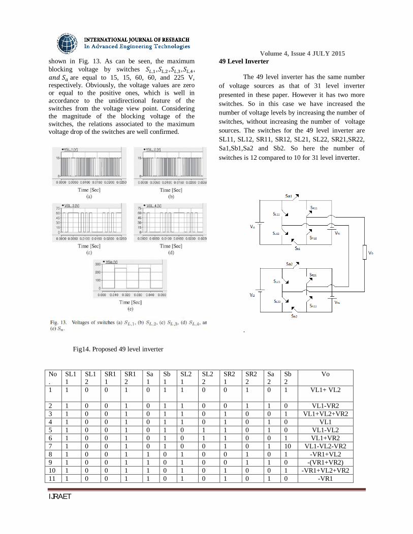
49 Level Inverter
The 49 level inverter has the same number of voltage sources as that of 31 level inverter presented in these paper. However it has two more switches. So in this case we have increased the number of voltage levels by increasing the number of switches, without increasing the number of voltage sources. The switches for the 49 level inverter are SL11, SL12, SR11, SR12, SL21, SL22, SR21,SR22, Sa1,Sb1,Sa2 and Sb2. So here the number of switches is 12 compared to 10 for 31 level inverter.
.
Fig14. Proposed 49 level inverter
No.
SL11
SL12
SR11
SR12
Sa1
Sb1
SL21
SL22
SR21
SR22
Sa2
Sb2
Vo
1 1 0 0 1 0 1 1 0 0 1 0 1 VL1+ VL2
2 1 0 0 1 0 1 1 0 0 1 1 0 VL1-VR2 3 1 0 0 1 0 1 1 0 1 0 0 1 VL1+VL2+VR2 4 1 0 0 1 0 1 1 0 1 0 1 0 VL1 5 1 0 0 1 0 1 0 1 1 0 1 0 VL1-VL2 6 1 0 0 1 0 1 0 1 1 0 0 1 VL1+VR2 7 1 0 0 1 0 1 0 0 1 0 1 10 VL1-VL2-VR2 8 1 0 0 1 1 0 1 0 0 1 0 1 -VR1+VL2 9 1 0 0 1 1 0 1 0 0 1 1 0 -(VR1+VR2) 10 1 0 0 1 1 0 1 0 1 0 0 1 -VR1+VL2+VR2 11 1 0 0 1 1 0 1 0 1 0 1 0 -VR1

Volume 4, Issue 4 JULY 2015
IJRAET
12 1 0 0 1 1 0 0 1 1 0 1 0 -VR1-VL2 13 1 0 0 1 1 0 0 1 1 0 0 1 -VR1+VR2 14 1 0 0 1 1 0 0 1 0 1 1 0 -
(VR1+VL2+VR2)
15 1 0 1 0 0 1 1 0 0 1 0 1 VL1+VR1+VL2 16 1 0 1 0 0 1 1 0 0 1 1 0 VL1+VR1-VR2 17 1 0 1 0 0 1 1 0 1 0 0 1 VL1+VR1+VL2
+VR2 18 1 0 1 0 0 1 1 0 1 0 1 0 VL1+VR1 19 1 0 1 0 0 1 0 1 1 0 1 0 VL1+VR1-VL2 20 1 0 1 0 0 1 0 1 1 0 0 1 VL1+VR1+VR2 21 1 0 1 0 0 1 0 1 0 1 1 0 VL1+VR1-VL2-
VR2 22 1 0 1 0 1 0 1 0 0 1 0 1 VL2 23 1 0 1 0 1 0 1 0 0 1 1 0 -VR2 24 1 0 1 0 1 0 1 0 1 0 0 1 VL2+VR2 25 1 0 1 0 1 0 1 0 1 0 1 0 0
No.
SL11
SL12
SR11
SR12
Sa1
Sb1
SL21
SL22
SR21
SR22
Sa2
Sb2
Vo
26 1 0 1 0 1 0 0 1 1 0 1 0 -VL2 27 1 0 1 0 1 0 0 1 1 0 0 1 VR2 28 1 0 1 0 1 0 0 1 0 1 1 0 -(VL2+VR2) 29 0 1 1 0 1 0 1 0 0 1 0 1 -VL1+VL2 30 0 1 1 0 1 0 1 0 0 1 1 0 -VL1-VR2 31 0 1 1 0 1 0 1 0 1 0 0 1 -VL1+VL2+VR2 32 0 1 1 0 1 0 1 0 1 0 1 0 -VL1 33 0 1 1 0 1 0 0 1 1 0 1 0 -VL1-VL2 34 0 1 1 0 1 0 0 1 1 0 0 1 -VL1+VR2 35 0 1 1 0 1 0 0 1 0 1 1 0 -VL1-(VL2+VR2) 36 0 1 1 0 0 1 1 0 0 1 0 1 VR1+VL2 37 0 1 1 0 0 1 1 0 0 1 1 0 VR1-VR2 38 0 1 1 0 0 1 1 0 1 0 0 1 VR1+VL2+VR2 39 0 1 1 0 0 1 1 0 1 0 1 0 VR1 40 0 1 1 0 0 1 0 1 1 0 1 0 VR1-VL2 41 0 1 1 0 0 1 0 1 1 0 0 1 VR1+VR2 42 0 1 1 0 0 1 0 1 0 1 1 0 VR1-(VL2+VR2) 43 0 1 0 1 1 0 1 0 0 1 0 1 -(VL1+VR1)+VL2 44 0 1 0 1 1 0 1 0 0 1 1 0 -(VL1+VR1)-VR2 45 0 1 0 1 1 0 1 0 1 0 0 1 -
(VL1+VR1)+VL2+VR2
46 0 1 0 1 1 0 1 0 1 0 1 0 -(VL1+VR1) 47 0 1 0 1 1 0 0 1 1 0 1 0 -(VL1+VR1)-VL1 48 0 1 0 1 1 0 0 1 1 0 0 1 -(VL1+VR1)+VR1 49 0 1 0 1 1 0 0 1 0 1 1 0 -(VL1+VR1)-
(VL2+VR2) The 49 level inverter can be understood
more clearly if we think it as two 7 level inverters connected in series. But the main difference is that
the output voltage or load is connected as shown in the figure 14. Whereas in case of seven level inverter the output voltage is connected in the middle of the

Volume 4, Issue 4 JULY 2015
IJRAET
circuit as shown in its figure. Here in 49 level inverter the magnitude of voltages sources are VL1= 10V, VL2=70V, VR1=20V and VR2=140V. The maximum voltage output is 240V. The 49 level inverter is basically two cascaded 7 level inverters, therefore its output is the sum of the two cascaded inverters. Lets us take that Vo1 is the output voltage of first seven level inverter and Vo2 is the output voltage of second seven level inverter, then the output of the 49 level inverter will be Vo1+ Vo2 . Keeping this in mind we can form the output table of the 49 level inverter as shown in Table III.
CONCLUSION In this paper, two basic topologies have been
proposed for multilevel inverters to generate seven voltage levels at the output. The basic topologies can be developed to any number of levels at the output where the 31-level, 127-level, and general topologies are consequently presented. In addition, a new algorithm to determine the magnitude of the dc voltage sources has been proposed. The proposed general topology was compared with the different kinds of presented topologies in literature from different points of view. According to the comparison results, the proposed topology requires a lesser number of IGBTs, power diodes, driver circuits, and dc voltage sources. Moreover, the magnitude of the blocking voltage of the switches is lower than that of conventional topologies. However, the proposed topology has a higher number of variety of dc voltage sources in comparison with the others. The performance accuracy of the proposed topology was verified through the PSCAD simulation and the experimental results of a 31-level inverter. Also a 49 level inverter with 12 swithces is proposed which has the same number of voltage sources as that of 31 level inverter to show that the number of levels can be increased without increasing the number of voltage sources. The same was verified through simulation.
REFERENCES [1] E. Babaei and S. H. Hosseini, “Charge balance control methods for asymmetrical cascade multilevel converters,” inProc. ICEMS, Seoul, Korea, 2007, pp. 74–79. [2] K. Wang, Y. Li, Z. Zheng, and L. Xu, “Voltage balancing and fluctuationsuppression methods of floating capacitors in a new modular multilevel
converter,”IEEE Trans. Ind. Electron., vol. 60, no. 5, pp. 1943–1954, May 2013. [3] J. Ebrahimi, E. Babaei, and G. B. Gharehpetian, “A new topology of cascaded multilevel converters with reduced number of components for high-voltage applications,”IEEE Trans. Power Electron., vol. 26, no. 11, pp. 3109–3118, Nov. 2011. [4] M. Manjrekar and T. A. Lipo, “A hybrid multilevel inverter topology for drive application,” inProc. APEC, 1998, pp. 523–529. [5] M. Narimani and G. Moschopoulos, “A novel single-stage multilevel type full-bridge converter,”IEEE Trans. Ind. Electron., vol. 60, no. 1, pp. 31– 42, Jan. 2013. [6] N. Abd Rahim, M. F. Mohamad Elias, and W. P. Hew, “Transistor-clamped H-bridge based cascaded multilevel inverter with new method of capacitor voltage balancing,”IEEE Trans. Ind. Electron., vol. 60, no. 8, pp. 2943–2956, Aug. 2013. [7] M. Farhadi Kangarlu and E. Babaei, “A generalized cascaded multilevel inverter using series connection of submultilevel inverters,” IEEE Trans. Power Electron., vol. 28, no. 2, pp. 625–636, Feb. 2013. [8] S. R. Pulikanti, G. Konstantinou, and V. G. Agelidis, “Hybrid seven-level cascaded active neutral-point-clamped-based multilevel converter under SHE-PWM,”IEEE Trans. Ind. Electron., vol. 60, no. 11, pp. 4794–4804, Nov. 2013. [9] Y. Hinago and H. Koizumi, “A single-phase multilevel inverter using switched series/parallel dc voltage sources,”IEEE Trans. Ind. Electron., vol. 57, no. 8, pp. 2643–2650, Aug. 2010. [10] G. Waltrich and I. Barbi, “Three-phase cascaded multilevel inverter using power cells with two inverter legs in series,”IEEE Trans. Ind. Appl., vol. 57, no. 8, pp. 2605–2612, Aug. 2010. [11] W. K. Choi and F. S. Kang, “H-bridge based multilevel inverter using PWM switching function,” inProc. INTELEC, 2009, pp. 1–5. [12] E. Babaei, M. Farhadi Kangarlu, and F. Najaty Mazgar, “Symmetric and asymmetric multilevel inverter topologies with reduced switching devices,”Elect. Power Syst. Res., vol. 86, pp. 122–130, May 2012. [13] J. Ebrahimi, E. Babaei, and G. B. Gharehpetian, “A new multilevel converter topology with reduced number of power electronic components,” IEEE Trans. Ind. Electron., vol. 59, no. 2, pp. 655–667, Feb. 2012. [14] E. Babaei, S. H. Hosseini, G. B. Gharehpetian, M. Tarafdar Haque, and M. Sabahi, “Reduction of DC voltage sources and switches in asymmetrical multilevel converters using a novel topology,”Elect.

Volume 4, Issue 4 JULY 2015
IJRAET
Power Syst. Res., vol. 77, no. 8, pp. 1073–1085, Jun. 2007.
Mr. MOHAMMED SALEEM , at present he is a Associate Professor in department of Electrical & Electronics Engineering, Aurora’s Scientific, Technological & Research Academy Hyderabad Andhra Pradesh, India. He received his B.Tech. degree in Electrical and Electronics Engineering from J.N.T.U Hyderabad in 2007, He recived his M.Tech(power electronics) Degree from J.N.T.U, Hyderabad India. His research interests accumulate in the area of Power Electronics, Drives, DC-DC Converters, AC-DC Converters and Renewable energy sources and Electrical Machines. Email Id : [email protected]
Mr. MOIRANGTHEM SAMSON completed his B.Tech in Electrical and Electronics Engineering in 2012 from RGCET, PONDICHERRY UNIVERSITY and is now persuing M.TECH in power system control and automation in JNTUH, hyderabad. His areas of interest includes power systems, renewable energy and robotics. E-mail id: [email protected]