cascaded multilevel converter based …etd.lib.metu.edu.tr/upload/12614941/index.pdf · cascaded...
TRANSCRIPT

CASCADED MULTILEVEL CONVERTER BASED TRANSMISSION
STATCOM: SYSTEM DESIGN METHODOLOGY AND DEVELOPMENT OF A
12kV ±12MVAr POWER-STAGE
A THESIS SUBMITTED TO
THE GRADUATE SCHOOL OF NATURAL AND APPLIED SCIENCES
OF
MIDDLE EAST TECHNICAL UNIVERSITY
BY
BURHAN GÜLTEKİN
IN PARTIAL FULFILLMENT OF THE REQUIREMENTS
FOR
THE DEGREE OF DOCTOR OF PHILOSOPHY
IN
ELECTRICAL AND ELECTRONICS ENGINEERING
SEPTEMBER 2012

ii
Approval of the thesis
CASCADED MULTILEVEL CONVERTER BASED TRANSMISSION
STATCOM: SYSTEM DESIGN METHODOLOGY AND DEVELOPMENT
OF A 12kV ±12MVAr POWER-STAGE
submitted by BURHAN GÜLTEKİN in partial fulfillment of the requirements for
the degree of Doctor of Philosophy in Electrical and Electronics Engineering
Department, Middle East Technical University by,
Prof. Dr. Canan ÖZGEN _________________
Dean, Graduate School of Natural and Applied Sciences
Prof. Dr. İsmet ERKMEN ________________
Head of Department, Electrical and Electronics Engineering
Prof. Dr. Muammer ERMİŞ ________________
Supervisor, Electrical and Electronics Engineering
Examining Committee Members :
Prof. Dr. H. Bülent ERTAN ____________________
Electrical and Electronics Engineering, METU
Prof. Dr. Muammer ERMİŞ ____________________
Electrical and Electronics Engineering, METU
Prof. Dr. Işık ÇADIRCI ____________________
Electrical and Electronics Engineering, Hacettepe University
Prof. Dr. Aydın ERSAK ____________________
Electrical and Electronics Engineering, METU
Prof. Dr.Arif ERTAŞ ____________________
Electrical and Electronics Engineering, METU
Date: 14-09-2012

iii
I hereby declare that all information in this document has been obtained and
presented in accordance with academic rules and ethical conduct. I also declare
that, as required by these rules and conduct, I have fully cited and referenced
all material and results that are not original to this work.
Name, Last name : Burhan GÜLTEKİN
Signature :
iv
ABSTRACT
CASCADED MULTILEVEL CONVERTER BASED TRANSMISSION
STATCOM: SYSTEM DESIGN METHODOLOGY AND DEVELOPMENT OF A
12kV ±12MVAr POWER-STAGE
GÜLTEKİN, Burhan
Ph.D., Department of Electrical and Electronics Engineering
Supervisor : Prof. Dr. Muammer ERMİŞ
September 2012, 177 pages
This research and development work deals with the design methodology for
Cascaded Multilevel Converter (CMC) based Transmission STATCOM (T-
STATCOM) and development of a ±12MVAR, 12kV line-to-line wye-connected,
11-level CMC. This CMC module constitutes the basic building block of T-
STATCOM systems. Sizing of the CMC module, number of H-Bridges in each phase
of the CMC, AC voltage rating of the CMC, the number of paralleled CMC modules
in the T-STATCOM system, optimum value of series filter reactors and
determination of busbar in the power grid to which the T-STATCOM system is
going to be connected are also discussed in the thesis in view of IEEE Std.519-1992,
current status of HV IGBT technology and the required reactive power variation
range for the T-STATCOM application. In the field prototype of the CMC module,
the AC voltages are approximated to sinusoidal waves by Selective Harmonic
Elimination Method (SHEM) and by the use of an optimized series input filter
reactor. The use of n number of HBs in each phase provides us n number of freedom
v
in the application of SHEM. One of them is allocated to the fundamental component
while n-1 is for the elimination of low order harmonics. Since n is chosen to five in
the prototype system, 5th, 7th,11th and 13th harmonic components are successfully
eliminated in the AC voltage waveforms of the CMC module. The equalization of
DC link capacitor voltages is achieved according to Modified Selective Swapping
(MSS) algorithm. MSS is applied every 400µs period if needed to obtain a perfect
equalization of DC link capacitor voltages at the expense of higher switching
frequency and hence switching losses. In this research work, an L-shaped laminated
bus has been designed and the HV IGBT driver circuit has been modified for
optimum switching performance of HV IGBT modules in each HB circuit. The
performances of the HB circuit and the resulting 11-level CMC module have been
obtained not only in the laboratory but also in the field. Design works for HB and the
CMC are based on MATLAB and PSCAD simulations. The laboratory and field
performance of the HB circuit and CMC module is found to be satisfactory and quite
consistent with the theoretical results and design objectives. In addition to these, 154
kV, ±50MVAr T-STATCOM prototype has been designed, implemented and
installed at Sincan Transformer Substation-Ankara primarily for the purposes of
reactive power compensation and terminal voltage regulation. The T-STATCOM
prototype is composed of five parallel operated CMC modules developed within the
scope of this PhD thesis research work. The T-STATCOM configuration permits the
operation of any number of CMC modules in the range from one to five for
experimental purposes. The performance of this T-STATCOM system is also
presented in this PhD thesis as a sample application.
Keywords: Transmission STATCOM, Cascaded Multilevel Converter (CMC),
Modified Selective Swapping (MSS)
vi
ÖZ
KASKAT ÇOK SEVİYELİ ÇEVİRGEÇ TABANLI İLETİM STATKOM:
SİSTEM TASARIM YÖNTEMİ VE BİR 12kV ±12MVAr GÜÇ KATI
GELİŞTİRİLMESİ
GÜLTEKİN, Burhan
Doktora, Elektrik Elektronik Mühendisliği Bölümü
Tez Yöneticisi : Prof. Dr. Muammer ERMİŞ
Eylül 2012, 177 sayfa
Bu araştırma ve geliştirme çalışması, H-Köprülü Çok Seviyeli Çevirgeç temelli
İletim STATCOM sistemleri için tasarım yöntemini ve bir adet ±12MVAR, 12 kV,
Y-bağlı, 11-seviyeli H-Köprülü Çok Seviyeli Çevirgeç yapısının geliştirilmesini
içermektedir. Geliştirilen bu çevirgeç modülü İletim STATCOM sistemleri için
temel bir yapı teşkil etmektedir. Ayrıca bu tezde, geliştirilen çok seviyeli çevirgecin
gücü, her fazında kullanılacak H-Köprü sayısı, çevirgecin tasarlanacağı AC gerilim
değeri, İletim STATCOM sisteminde kullanılacak paralel çevirgeç sayısı, modüle
bağlanacak en uygun seri filtre reaktörü değeri ve T-STATCOM’un güç sisteminde
bağlanacağı baranın belirlenmesi konuları IEEE 519-1992 standardı, YG IGBT’lerin
güncel teknolojisi ve uygulama için istenen reaktif gücün değişim aralağına göre
irdelenmiştir. Geliştirilen çok seviyeli çevirgecin AC gerilim şekilleri, Seçici
Harmonik Eleme Metodu (SHEM) ve en uygun değerdeki seri filtre reaktörünün
kullanılması ile sinüs dalgalarına yaklaştırılmıştır. Her faz için n tane H-Köprü
kullanımı SHEM uygulaması için n tane eşitliğin kullanım özgürlüğünü

vii
tanımaktadır. Bu eşitliklerden biri temel bileşen için kullanılırken geri kalan n-1
tanesi de düşük dereceli harmoniklerin yok edilmesi amacıyla kullanılabilmektedir.
Geliştirilen prototip sistem için n sayısı beş olarak seçildiğinden çevirgeç çıkış
gerilimlerinde 5., 7., 11. ve 13.harmonik bileşenleri başarılı bir şekilde elenmiştir.
Çevirgeçte kullanılan DA bağ kondansatör gerilimleri Düzenlemiş Seçici Yer
Değiştirmeli algoritması ile eşitlenmiştir. Gerektiğinde 400µs periyotlarla uygulanan
bu metod sayesinde yüksek anahtarlama frekansı ve daha fazla kayba rağmen DA
bağ gerilimleri için mükemmel bir eşitlik sağlanmıştır. Bu araştırma çalışmasında her
H-Köprü için L şeklinde bir lamine bara yapısı tasarlanmış ve YG IGBT’lerde
optimum anahtarlama performansı elde etmek için sürücü devreleri değiştirilmiştir.
H-Köprü ve elde edilen 11-seviyeli Çevrigeç performansları hem laboratuvarda hem
de sahada elde edilmiştir. H-Köprü ve çevirgeç için MATLAB ve PSCAD
benzetimleri ile tasarım çalışmaları yürütülmüştür. Laboratuvar ve sahada elde edilen
verilerin hem H-Köprü hem de çevirgeç için oldukça tatminkar olmasının yanısıra
teorik sonuçlar ve tasarım hedefleriyle gayet uyumlu olduğu gözlemlenmiştir.
Bunlara ek olarak, bir adet 154 kV, ±50MVAr İletim STATCOM prototipi tasarlanıp
geliştirilmiş ve Ankara’da bulunan Sincan Trafo Merkezinde reaktif güç
kompanzasyonu ve bara gerilim düzenlenmesi amaçları için kurulmuştur. Kurulan
sistem bu doktora tez çalışmasında geliştirilen beş adet çok seviyeli çevirgecin
paralel kullanımından oluşmaktadır. İletim STATCOM yapısı, birden beşe kadar
çevirgecin deneysel amaçla kullanılmasına olanak vermektedir. Bu İletim
STATCOM sisteminin performansı da ayrıca bir uygulama örneği olarak da tezde
verilmiştir.
Anahtar Kelimeler: İletim STATKOM, Çok Seviyeli Çevirgeçler, Düzenlenmiş
Seçici Yerdeğiştirme

viii
ACKNOWLEDGMENTS
I would like to express my deepest gratitude to my supervisor Prof. Dr. Muammer
Ermiş not only for his guidance, criticism, encouragements and insight throughout
this research but also for his continuous confidence in me, and his unforgettable and
valuable contributions to my career.
I would like to show my gratitude also to Prof. Dr. Işık Çadırcı for her guidance,
criticism, encouragements and insight throughout this research.
I would like to thank Prof. Dr. H. Bülent Ertan for his suggestions and comments in
my thesis progress committee.
The prototype system, developed within the scope of this research work, is a part of
the National Power Quality Project (Project No: 105G129). I would like to express
my special thanks to the Public Research Grant Committee (KAMAG) of TÜBİTAK
for their full financial support.
Special thanks to Turkish Electricity Transmission Co. (TEİAŞ) for their courage to
give us a chance to apply this novel technology. I am especially thankful to Yener
Akkaya, Semih Bideci and Hikmet Toygar and the other staff of TEİAŞ for their
great effort to design and installation of high voltage switchgears and to finish the
civil works of the system in a short time.
The assistance of the valuable staff in Power Electronics Department of TUBITAK
UZAY is gratefully acknowledged. I am especially thankful to all technical staff for
their substantial assistance and companionship during development and field tests of
prototype system.

ix
I would like to acknowledge my colleagues for their crucial contributions to this
research work: Cem Özgür Gerçek for his contribution to computer simulations,
Tevhid Atalık for his contribution to designing and programming the DSP Boards,
Mustafa Deniz for his contribution to designing and programming the FPGA Boards,
Erkan Koç for his contribution to design and implementation the PLC based
monitoring system, Nazan Biçer for her contribution to the power stage design and
production, Kemal Nadir Köse for his contribution to design and production of Water
Cooling System, Adnan Açık for his contribution to the design of capacitor
protection circuit and finally Cezmi Ermiş for his contribution to the design and
construction of the concrete platform of the developed STATCOM.
I would like to express my deepest gratitude to my family for their patience,
sacrifice, encouragement and continuous morale support.
Finally, I would like to express my deepest gratitude to my wife Şehnaz and my son
Birol Salih for their presence, patience, sacrifice, endless support and
encouragement.

x
TABLE OF CONTENTS
PLAGIARISM .................................................................................................... iii
ABSTRACT ......................................................................................................... iv
ÖZ ................................................................................................................... vi
ACKNOWLEDGEMENTS ................................................................................ viii
LIST OF TABLES .............................................................................................. xiii
LIST OF FIGURES ............................................................................................ xv
NOMENCLATURE ............................................................................................ xxiii
ABBREVIATIONS ............................................................................................. xxiv
CHAPTERS
1. INTRODUCTION ......................................................................................... 1
1.1.Overview ................................................................................................... 1
1.2.Scope of the Thesis ................................................................................... 11
2. OPERATING PRINCIPLES OF CMC BASED TRANMISSION
STATCOM .................................................................................................... 14
2.1.System Description ................................................................................... 14
2.2.Active and Reactive Power Control .......................................................... 16
2.3.Wave Shaping ........................................................................................... 22
2.4.Voltage Balancing of DC Link Capacitors ............................................... 31
2.4.1. Some Conventional Methods ........................................................ 31
2.4.2. Conventional Selective Swapping (CSS) Method ........................ 34
2.4.3. Modified Selective Swapping (MSS) Method .............................. 41
3. SYSTEM DESIGN AND SIZING ............................................................... 50
3.1. Introduction .............................................................................................. 50
3.2. Determination of Connection Point and Sizing of T-STATCOM ........... 50
3.3. Sizing of CMC Module ............................................................................ 53
3.4.Design of Series Filter Reactor ................................................................. 56
3.4.1. THD Values in AC Input Voltage of CMC .................................. 56
xi
3.4.2. Effect of Series Filter Inductance on THD and TDD ................... 58
3.4.3. Effect of Series Filter Inductance on DC Link Voltage
and Modulation Index Values ....................................................... 63
3.4.4. Effect of Series Filter Inductance on AC Input Voltage of CMC . 66
3.4.5. Conclusions ................................................................................... 67
4. DESIGN OF A CASCADED MULTILEVEL
CONVERTER (CMC) MODULE ............................................................... 70
4.1. Design of CMC Module........................................................................... 70
4.1.1. Design of the H-Bridge (HB) Circuit ............................................ 71
4.1.1.1.The structure and operation of HB Circuits ............................ 72
4.1.1.2.L-shaped Laminated Bus Design with 3-conducting Layers .. 79
4.1.1.3.Selection of Power Semiconductor Switches .......................... 82
4.1.1.4.Optimization of IGBT Switching Waveforms ........................ 89
4.1.1.5.Choice of DC Link Capacitor ................................................. 92
4.2. Design of Control System ........................................................................ 101
4.2.1. DSP Board ..................................................................................... 104
4.2.2. FPGA Board .................................................................................. 107
4.2.3. Programmable Logic Controller (PLC) ........................................ 108
4.3. Switching Strategies for the Application of Selective Swapping ............ 109
5. THE IMPLEMENTATION OF T-STATCOM SYSTEM AND
FIELD PERFORMANCE RESULTS ......................................................... 116
5.1.The Implementation of T-STATCOM System ......................................... 116
5.1.1. Power System Characteristics ....................................................... 120
5.2. Field Performance Results ....................................................................... 125
5.2.1. Field Performance of HB .............................................................. 125
5.2.1.1.Switching Waveforms of IGBT Modules ............................... 128
5.2.1.2.DC Link Current and Voltage Waveforms ............................. 129
5.2.2. Field Performance of CMC Module ............................................. 130
5.2.2.1.Voltage Waveforms at the Input of CMC ............................... 130
5.2.2.2.Transient Performance of CMC Module................................. 137
5.2.2.3.Performance of Selective Swapping Methods on

xii
Balancing DC Link Capacitor Voltages ................................... 139
5.2.3. Field Performance of T-STATCOM System ................................ 145
5.2.3.1.Voltage and Current Waveforms at MV (10.5 kV)
and HV (154 kV) sides ............................................................. 145
5.2.3.2.Voltage and Current Harmonics at PCC (154 kV).................. 147
5.2.3.3.Effects of Series Reactors on Voltage Harmonics .................. 148
5.2.3.4.Terminal Voltage Regulation (V-mode) ................................. 149
5.2.3.5.Reactive Power Compensation (Q-mode) ............................... 151
5.2.3.6.Transitions Between Full Capacitive
and Full Inductive Modes ......................................................... 153
6. CONCLUSIONS ........................................................................................... 155
REFERENCES .............................................................................................. 162
APPENDICES
A. SHEM EQUATIONS FOR 11-LEVEL CMC ........................................... 170
B. PERMISSIBLE REGINOS FOR THD AND TDD RECOMENDED
BY IEEE STD.519-1992 ........................................................................... 172
C. RATINGS OF COMMERCIALLY AVAILABLE HV IGBTS ................ 173
D. SOAS OF MITSUBISHI CM1200HC-66H HV IGBT MODULE ........... 174
CIRRICULUM VITAE ................................................................................ 175
xiii
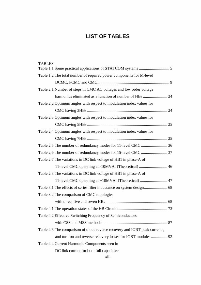
LIST OF TABLES
TABLES
Table 1.1 Some practical applications of STATCOM systems .............................. 5
Table 1.2 The total number of required power components for M-level
DCMC, FCMC and CMC ....................................................................... 9
Table 2.1 Number of steps in CMC AC voltages and low order voltage
harmonics eliminated as a function of number of HBs ........................ 24
Table 2.2 Optimum angles with respect to modulation index values for
CMC having 3HBs ............................................................................... 24
Table 2.3 Optimum angles with respect to modulation index values for
CMC having 5HBs ............................................................................... 25
Table 2.4 Optimum angles with respect to modulation index values for
CMC having 7HBs ............................................................................... 25
Table 2.5 The number of redundancy modes for 11-level CMC .......................... 36
Table 2.6 The number of redundancy modes for 15-level CMC .......................... 37
Table 2.7 The variations in DC link voltage of HB1 in phase-A of
11-level CMC operating at -10MVAr (Theoretical) ............................ 46
Table 2.8 The variations in DC link voltage of HB1 in phase-A of
11-level CMC operating at +10MVAr (Theoretical) ........................... 47
Table 3.1 The effects of series filter inductance on system design ....................... 68
Table 3.2 The comparison of CMC topologies
with three, five and seven HBs ............................................................. 68
Table 4.1 The operation states of the HB Circuit.................................................. 73
Table 4.2 Effective Switching Frequency of Semiconductors
with CSS and MSS methods ................................................................. 87
Table 4.3 The comparison of diode reverse recovery and IGBT peak currents,
and turn-on and reverse recovery losses for IGBT modules ................ 92
Table 4.4 Current Harmonic Components seen in
DC link current for both full capacitive

xiv
and full inductive operation modes ...................................................... 99
Table 4.5 Technical Specifications of IC Boards in Figure 4.24 ........................ 102
Table 5.1 The technical specifications of the installed T-STATCOM system ... 117
Table 5. 2 The electrical characteristics of the power system
at which T-STATCOM system is connected ...................................... 119
Table 5.3 The monthly maximum reactive power variations of
the PCC from Nov.2008 to June.2009 ................................................ 121
Table 5.4 CMC voltage harmonics at +10MVAr ............................................... 135
Table 5.5 CMC voltage harmonics at -10MVAr ................................................ 135
Table 5.6 Performance of selective swapping algorithms .................................. 142
Table 5.7 PCC line-to-ground voltage harmonics measured
by RCVT sensors ................................................................................ 146
Table 5.8 154kV side current harmonics at rated power
(IL=188A, ISC=20kA) .......................................................................... 147
Table 5.9 10.5kV voltage harmonics measured by RCVT sensors..................... 148
Table 5.10 CMC current harmonics at rated power ............................................ 148
Table 6.1 Effect of main system parameters on cost and performance .............. 161
Table 6.1 (Cont’d) Effect of main system parameters
on cost and performance ..................................................................... 162
xv
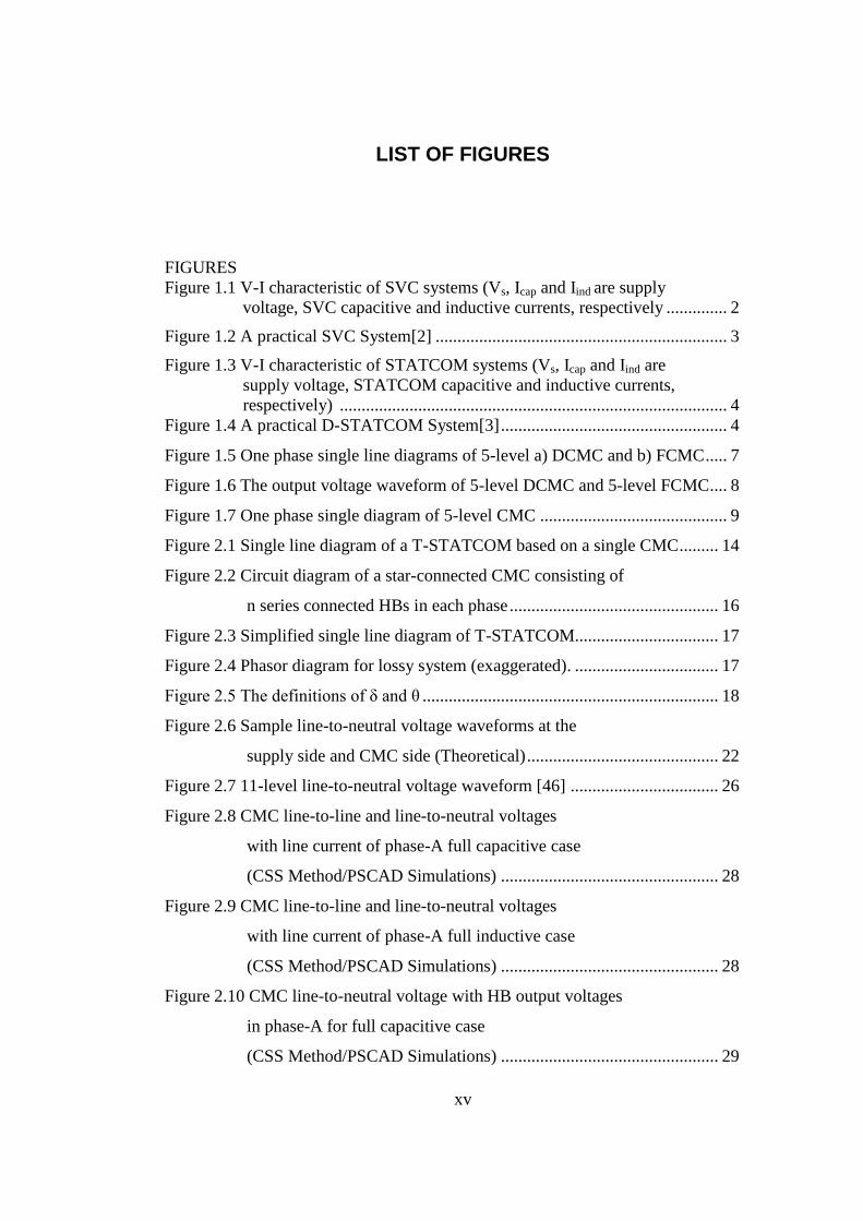
LIST OF FIGURES
FIGURES
Figure 1.1 V-I characteristic of SVC systems (Vs, Icap and Iind are supply
voltage, SVC capacitive and inductive currents, respectively .............. 2
Figure 1.2 A practical SVC System[2] ................................................................... 3
Figure 1.3 V-I characteristic of STATCOM systems (Vs, Icap and Iind are
supply voltage, STATCOM capacitive and inductive currents,
respectively) ......................................................................................... 4
Figure 1.4 A practical D-STATCOM System[3] .................................................... 4
Figure 1.5 One phase single line diagrams of 5-level a) DCMC and b) FCMC ..... 7
Figure 1.6 The output voltage waveform of 5-level DCMC and 5-level FCMC .... 8
Figure 1.7 One phase single diagram of 5-level CMC ........................................... 9
Figure 2.1 Single line diagram of a T-STATCOM based on a single CMC ......... 14
Figure 2.2 Circuit diagram of a star-connected CMC consisting of
n series connected HBs in each phase ................................................ 16
Figure 2.3 Simplified single line diagram of T-STATCOM................................. 17
Figure 2.4 Phasor diagram for lossy system (exaggerated). ................................. 17
Figure 2.5 The definitions of δ and θ .................................................................... 18
Figure 2.6 Sample line-to-neutral voltage waveforms at the
supply side and CMC side (Theoretical) ............................................ 22
Figure 2.7 11-level line-to-neutral voltage waveform [46] .................................. 26
Figure 2.8 CMC line-to-line and line-to-neutral voltages
with line current of phase-A full capacitive case
(CSS Method/PSCAD Simulations) .................................................. 28
Figure 2.9 CMC line-to-line and line-to-neutral voltages
with line current of phase-A full inductive case
(CSS Method/PSCAD Simulations) .................................................. 28
Figure 2.10 CMC line-to-neutral voltage with HB output voltages
in phase-A for full capacitive case
(CSS Method/PSCAD Simulations) .................................................. 29

xvi
Figure 2.11 CMC line-to-neutral voltage with HB output voltages
in phase-A for full inductive case
(CSS Method/PSCAD Simulations) .................................................. 30
Figure 2.12 The α/∆α method for DC link capacitor balancing [48] .................... 31
Figure 2.13 The rotational angle method for DC link capacitor balancing [49] ... 33
Figure 2.14 The rotational of switching angles [49] ............................................. 33
Figure 2.15 Redundant Modes of a)+3Vd and b) 0Vd levels ................................ 35
Figure 2.16 Redundant Modes of +1Vd level ....................................................... 35
Figure 2.17 Redundant Modes of +2Vd level ....................................................... 36
Figure 2.18 The variations in the instantaneous DC link voltages of
a) phase-A, b) phase-B and c) phase-C HBs of 11-level CMC
for full capacitive case (PSCAD Simulations) ................................... 39
Figure 2.19 The variations in the instantaneous DC link voltages of
a) phase-A, b) phase-B and c) phase-C HBs of 11-level CMC
for full inductive case (PSCAD Simulations) .................................... 40
Figure 2.20 The variations in the instantaneous DC link voltages of
1st HBs in three phases of 11-level CMC for
a) full inductive, b) full capacitive cases (PSCAD Simulations) ....... 41
Figure 2.21 The illustration of CSS and MSS ...................................................... 42
Figure 2.22 The flowchart for MSS method employed in M-level CMC ............. 43
Figure 2.23 The variations in the instantaneous DC link voltages of
the CMC under a) CSS, b) MSS with ∆ts=400 µs and
c) MSS with ∆ts=200 µs for full capacitive case
(PSCAD Simulations) ........................................................................ 44
Figure 2.24 The variations in the instantaneous DC link voltages of
the CMC under a) CSS, b) MSS with ∆ts=400 µs and
c) MSS with ∆ts=200 µs for full inductive case
(PSCAD Simulations) ........................................................................ 45
Figure 2.25 The performance of CSS and MSS methods on the instantaneous
peak-to-peak variations in the DC link voltage of an HB unit
(Theoretical) ....................................................................................... 48

xvii
Figure 3.1 Connection alternatives for T-STATCOM system ((a) and
(b) connection to the MV side of existing power transformer) .......... 51
Figure 3.2 Connection alternatives for T-STATCOM system ((a),(b),and (c)
connection to the power grid via a special coupling transformer) ..... 52
Figure 3.3 Maximum attainable CMC ratings calculated as a function of rated
AC voltage of CMC (Vc) for three different CMC topologies
(in view of HV IGBT technology by June 2012) ............................... 55
Figure 3.4 THD variations against series inductance for AC input voltage
of CMC Topologies ((a) Capacitive Case; (b) Inductive Case) ......... 58
Figure 3.5 THD variations against series inductance for CMC Topologies
at MV PCC ((a) Capacitive Case; (b) Inductive Case) ...................... 59
Figure 3.6 TDD variations against series inductance for CMC Topologies
at MV PCC ((a) Capacitive Case; (b) Inductive Case) ...................... 60
Figure 3.7 THD variations against total series inductance for CMC Topologies
at HV PCC ((a) Capacitive Case; (b) Inductive Case) ....................... 61
Figure 3.8 TDD variations against total series inductance for CMC Topologies
at HV PCC ((a) Capacitive Case; (b) Inductive Case) ....................... 62
Figure 3.9 Variations in DC link voltage against total series inductance
for different values of modulation index,
M in the case of CMC with 3HBs/Theoretical ................................... 64
Figure 3.10 Variations in DC link voltage against total series inductance
for different values of modulation index,
M in the case of CMC with 7HBs/Theoretical ................................... 64
Figure 3.11 Variations in DC link voltage against total series inductance
for different values of modulation index, M
in the case of CMC with 5HBs/Theoretical ....................................... 65
Figure 3.12 Effect of series filter inductance on CMC input voltage ................... 66
Figure 4.1 Designed and implemented 3-phase, 12kV, ±12 MVAr
Y-connected 11-level CMC module .................................................. 71
Figure 4.2 Single line diagram of (a) the HB Circuit
and (b) its typical output voltage ........................................................ 73

xviii
Figure 4.3 The operation modes of HB: a) Charging-1(CH1),
b) Charging-2(CH2) ,c) Discharging-1 (DCH1),
d) Discharging-2 (DCH2), e) By-pass-1 (BYP1),
f) By-pass-2 (BYP2), g) By-pass-3 (BYP3), h) By-pass-4 (BYP4) .. 74
Figure 4.4 11-level line-to-neutral voltage waveform
with definition and sequence of HB operation modes
for capacitive operation of the CMC .................................................. 75
Figure 4.5 11-level line-to-neutral voltage waveform
with definition and sequence of HB operation modes
for inductive operation of the CMC ................................................... 76
Figure 4.6 Voltage spikes superimposed on the line-to-neutral CMC
voltages with MSS method (∆ts =400µs, field data) ......................... 77
Figure 4.7 Line-to-neutral voltage and line current waveforms
recorded in the field at 154kV PCC ................................................... 78
Figure 4.8 General view (a) and structure (b) of the designed HB ....................... 79
Figure 4.9 Performance of HB in the Laboratory (a)Test Circuit,
and (b) switching waveforms of IGBT1, D1and IGBT2 ................... 81
Figure 4.10 Power semiconductors current, HB output voltage and CMC l-to-n
voltage waveforms for Q=-10MVAr at PCC with CSS method
(PSCAD Simulations) ........................................................................ 83
Figure 4.11 Power semiconductors current, HB output voltage and CMC l-to-n
voltage waveforms for Q=+10MVAr at PCC with CSS method
(PSCAD Simulations) ........................................................................ 83
Figure 4.12 Power semiconductors current, HB output voltage and CMC l-to-n
voltage waveforms for Q=-10MVAr at PCC with MSS method at
∆ts=400µs (PSCAD Simulations) ...................................................... 84
Figure 4.13 Power semiconductors current, HB output voltage and CMC l-to-n
voltage waveforms for Q=+10MVAr at PCC with MSS method at
∆ts=400µs (PSCAD Simulations) ....................................................... 84

xix
Figure 4.14 Power semiconductors current, HB output voltage and CMC l-to-n
voltage waveforms for Q=-10MVAr at PCC with MSS method
∆ts=200µs (PSCAD Simulations) ...................................................... 85
Figure 4.15 Power semiconductors current, HB output voltage and CMC l-to-n
voltage waveforms for Q=+10MVAr at PCC with MSS method at
∆ts=200µs (PSCAD Simulations) ...................................................... 85
Figure 4.16 Relationship of FIT values and applied DC link voltages for
CM1200HC-66H HV IGBT [55] ....................................................... 88
Figure 4.17 The switching waveforms during turn-on of IGBT2 with standard
gate driver circuit at nearly Ic(rated) .................................................. 90
Figure 4.18 The switching waveforms during turn-on of IGBT2 with modified
gate driver circuit at nearly Ic(rated) .................................................. 91
Figure 4.19 The variations in peak-to-peak voltage
ripple against capacitance value ......................................................... 93
Figure 4.20 The variations in DC link voltage and current of HB1
with its output voltage for Q=-10 MVAr at PCC
(PSCAD Simulations) ........................................................................ 95
Figure 4.21 The variations in DC link voltage and current of HB1
with its output voltage for Q=+10 MVAr at PCC
(PSCAD Simulations) ........................................................................ 96
Figure 4.22 The variations of harmonic components in DC link voltage
and current for Q=-10 MVAr at PCC (PSCAD Simulations) ............ 97
Figure 4.23 The variations of harmonic components in DC link voltage
and current for Q=+10 MVAr at PCC (PSCAD Simulations) ........... 98
Figure 4.24 The block diagram of the digital control system of CMC
with control panel ............................................................................. 101
Figure 4.25 The diagram of control system for the designed CMC module....... 103
Figure 4.26 Generation of Qref and Qc by DSP Board ........................................ 104
Figure 4. 27 PLL generation by the DSP Board ................................................. 105
Figure 4.28 Illustration of a) operation modes of IGBT modules in phase-A
of the CMC before (Mode-1), during (Mode-2) and
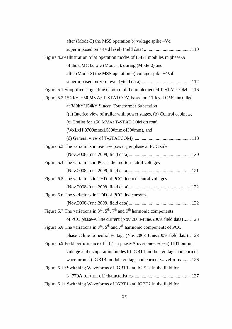
xx
after (Mode-3) the MSS operation b) voltage spike –Vd
superimposed on +4Vd level (Field data) ........................................ 110
Figure 4.29 Illustration of a) operation modes of IGBT modules in phase-A
of the CMC before (Mode-1), during (Mode-2) and
after (Mode-3) the MSS operation b) voltage spike +4Vd
superimposed on zero level (Field data) .......................................... 112
Figure 5.1 Simplified single line diagram of the implemented T-STATCOM ... 116
Figure 5.2 154 kV, ±50 MVAr T-STATCOM based on 11-level CMC installed
at 380kV/154kV Sincan Transformer Substation
((a) Interior view of trailer with power stages, (b) Control cabinets,
(c) Trailer for ±50 MVAr T-STATCOM on road
(WxLxH:3700mmx16800mmx4300mm), and
(d) General view of T-STATCOM) ................................................. 118
Figure 5.3 The variations in reactive power per phase at PCC side
(Nov.2008-June.2009, field data) ..................................................... 120
Figure 5.4 The variations in PCC side line-to-neutral voltages
(Nov.2008-June.2009, field data) ..................................................... 121
Figure 5.5 The variations in THD of PCC line-to-neutral voltages
(Nov.2008-June.2009, field data) ..................................................... 122
Figure 5.6 The variations in TDD of PCC line currents
(Nov.2008-June.2009, field data) ..................................................... 122
Figure 5.7 The variations in 3rd
, 5th
, 7th
and 9th
harmonic components
of PCC phase-A line current (Nov.2008-June.2009, field data) ...... 123
Figure 5.8 The variations in 3rd
, 5th
and 7th
harmonic components of PCC
phase-C line-to-neutral voltage (Nov.2008-June.2009, field data) .. 123
Figure 5.9 Field performance of HB1 in phase-A over one-cycle a) HB1 output
voltage and its operation modes b) IGBT1 module voltage and current
waveforms c) IGBT4 module voltage and current waveforms ........ 126
Figure 5.10 Switching Waveforms of IGBT1 and IGBT2 in the field for
Ic=770A for turn-off characteristics ................................................. 127
Figure 5.11 Switching Waveforms of IGBT1 and IGBT2 in the field for
xxi
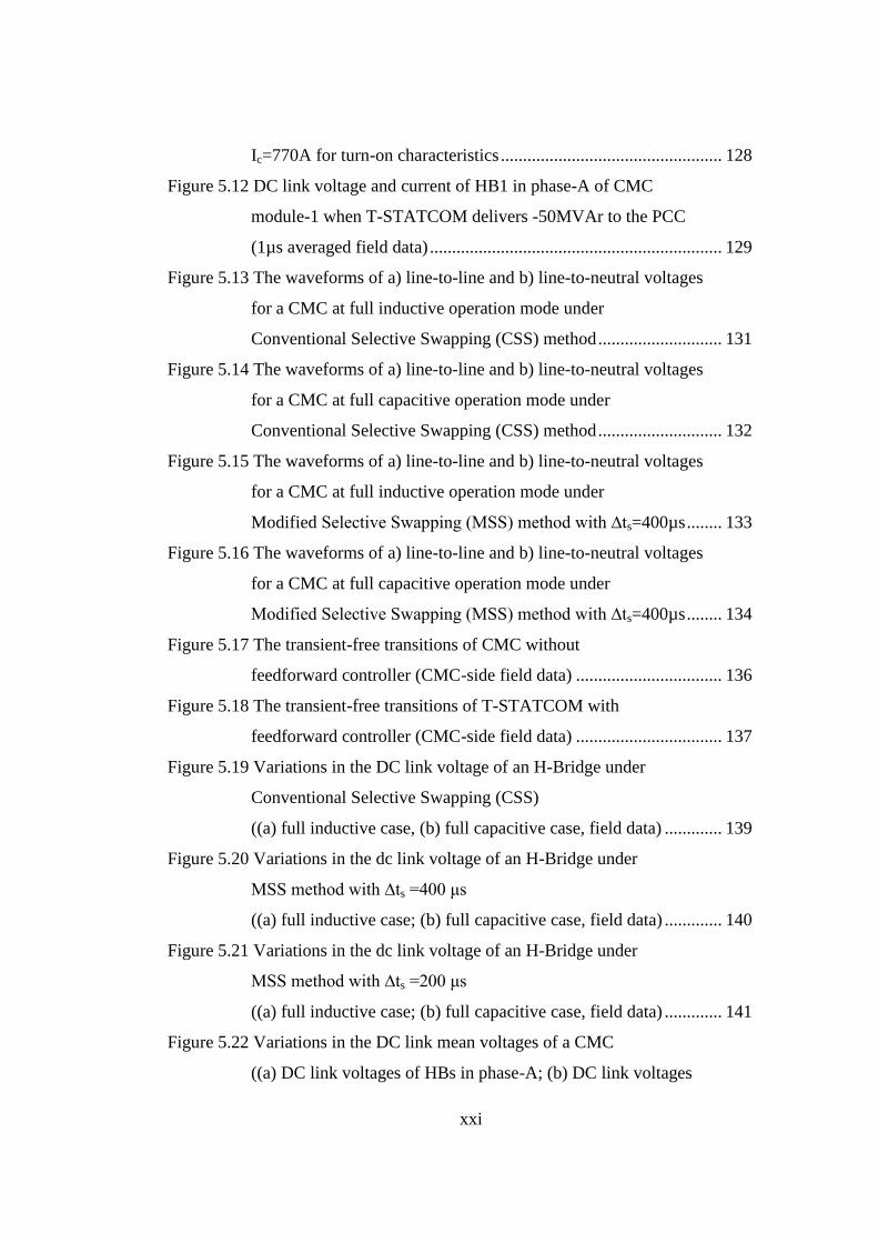
Ic=770A for turn-on characteristics .................................................. 128
Figure 5.12 DC link voltage and current of HB1 in phase-A of CMC
module-1 when T-STATCOM delivers -50MVAr to the PCC
(1µs averaged field data) .................................................................. 129
Figure 5.13 The waveforms of a) line-to-line and b) line-to-neutral voltages
for a CMC at full inductive operation mode under
Conventional Selective Swapping (CSS) method ............................ 131
Figure 5.14 The waveforms of a) line-to-line and b) line-to-neutral voltages
for a CMC at full capacitive operation mode under
Conventional Selective Swapping (CSS) method ............................ 132
Figure 5.15 The waveforms of a) line-to-line and b) line-to-neutral voltages
for a CMC at full inductive operation mode under
Modified Selective Swapping (MSS) method with ∆ts=400µs ........ 133
Figure 5.16 The waveforms of a) line-to-line and b) line-to-neutral voltages
for a CMC at full capacitive operation mode under
Modified Selective Swapping (MSS) method with ∆ts=400µs ........ 134
Figure 5.17 The transient-free transitions of CMC without
feedforward controller (CMC-side field data) ................................. 136
Figure 5.18 The transient-free transitions of T-STATCOM with
feedforward controller (CMC-side field data) ................................. 137
Figure 5.19 Variations in the DC link voltage of an H-Bridge under
Conventional Selective Swapping (CSS)
((a) full inductive case, (b) full capacitive case, field data) ............. 139
Figure 5.20 Variations in the dc link voltage of an H-Bridge under
MSS method with ∆ts =400 μs
((a) full inductive case; (b) full capacitive case, field data) ............. 140
Figure 5.21 Variations in the dc link voltage of an H-Bridge under
MSS method with ∆ts =200 μs
((a) full inductive case; (b) full capacitive case, field data) ............. 141
Figure 5.22 Variations in the DC link mean voltages of a CMC
((a) DC link voltages of HBs in phase-A; (b) DC link voltages

xxii
of HB1s in three phases, Field data) ................................................ 143
Figure 5.23 Line-to-neutral voltage and line current waveforms at MV side of
T-STATCOM ((a) full inductive; (b) full capacitive, field data) ..... 144
Figure 5.24 Line-to-neutral voltage and line current waveforms at HV side of
T-STATCOM ((a) full inductive; (b) full capacitive, field data) ..... 145
Figure 5.25 The performance of T-STATCOM in V-mode (Field data) ............ 149
Figure 5.26 The performance of T-STATCOM in Q-mode (Field data) ............ 151
Figure 5.27 Transition from a) from full inductive to full capacitive
(10.5 kV side, field data) b) full capacitive to
full inductive (154 kV side, field data) ............................................ 152
Figure 5.28 Variations in line-to-ground voltage and current during the transition
from full inductive to full capacitive (10.5 kV side, field data) ....... 153
Figure 5.29 Variations in line-to-ground voltage and current during the transition
from full capacitive to full inductive (10.5 kV side, field data) ....... 154
Figure B.1 Permissible regions for total harmonic distortion (THD) and total
demand distortion (TDD) as a function of rated voltage
at point of common coupling (PCC) as recommended
by IEEE Std.519, 1992 ..................................................................... 172
Figure C.1 Collector current and collector-emitter voltage ratings of commercially
available High Voltage Insulated Gate Bipolar Transistors
(HV IGBTs) by June 2012 with respect to
DC link voltages of HB .................................................................... 173
Figure D.1 Safe Operating Areas (SOA) of HV IGBT modules specified in
datasheet of MITSUBISHI CM1200HC-66H .................................. 174
xxiii
NOMENCLATURE
Es′: Internal source voltage referred to CMC side
Xs′: Internal source reactance referred to CMC side
PCC: Point of Common Coupling
Vs′: Fundamental voltage component at Point of Common Coupling (PCC)
referred to CMC side
X: Total series reactance including leakage reactance of the coupling transformer
referred to CMC side and reactance of input filter reactors
R: Total series resistance including internal resistance of the coupling
transformer referred to CMC side and internal resistance of the input filter
reactors
Vc: Fundamental component of the CMC AC voltage
Ic: Fundamental component of the CMC line current
θ: Phase angle between and
δ: Power angle between and .
Z: Impedance angle, tan-1
(X/R)
Ps, Qs: Active and reactive power inputs to T-STATCOM at PCC
Pc, Qc:Active and reactive power inputs to CMC

xxiv
ABBREVIATIONS
FACTS Flexible AC Transmission Systems
SVC Static VAr Compensators
STATCOM Static Synchronous Compensators
SC Synchronous Condensers
TCR Thyristor Controlled Reactor
D-STATCOM Distribution type STATCOM
GTO Gate Turn-off thyristors
IGBT Insulated Gate Bipolar Transistors
IEGT Injection Enhanced Insulated Gate Transistor
IGCT Integrated Gate Commutated Thyristors
MV Medium Voltage
T-STATCOM Transmission type STATCOM
MC Multilevel Converter
DCMC Diode Clamped Multilevel Converters
FCMC Flying Capacitor Multilevel Converters
CMC Cascaded Multilevel Converters
HB H-Bridge
THD Total Harmonic Distortion
PCC Point of Common Coupling
TDD Total Demand Distortion
SHEM Selective Harmonic Elimination Method
CSS Conventional Selective Swapping
MSS Modified Selective Swapping
ESL Equivalent Series Inductance
ESR Equivalent Series Resistance
RCVT RC Type Voltage Transformer

1
CHAPTER 1
INTRODUCTION
1.1 Overview
Flexible AC Transmission Systems (FACTS) has been defined by the IEEE [1] as a
power electronic based system and other static equipment that provide control of one
or more AC transmission system parameters to enhance controllability and increase
power transfer capability. Nowadays, FACTS are being increasingly used in power
systems, to enhance the system utilization and power transfer capacity as well as the
stability, security, reliability and power quality of AC system interconnections.
In general, FACTS controllers can be divided into three categories:
1. Series controllers,
2. Shunt controllers
3. Combined series-shunt controllers.
Among FACTS controllers, the shunt controllers have widely been used because of
their problem-solving capabilities from transmission to distribution levels. It is well
known that by using appropriate amount of compensated reactive current or power,
the transmitted power carrying capacity can be increased and the voltage profile of
the transmission line can be controlled. Also, shunt controllers can improve transient

2
stability, and damp power oscillations for the interconnected transmission networks.
For distribution networks, they are mainly used for the purposes of power factor
correction, flicker mitigation, load balancing and harmonic mitigation.
Shunt controllers can be classified as Static VAr Compensators (SVC) and Static
Synchronous Compensators (STATCOM). SVCs use synchronously connected
inductor and/or capacitor banks and absorb/generate controllable reactive power. The
reactive power is dependent upon the system parameters especially it is directly
proportional to the source voltage and any decrease in the source voltage reduce the
inductive and reactive current components as shown in Figure 1.1 and hence
decreases the reactive power compensation capability of SVC system Figure 1.2
shows a practical
Figure 1.1 V-I characteristic of SVC systems (Vs, Icap and Iind are supply
voltage, SVC capacitive and inductive currents, respectively)
IcapIcap1Icap2
IindIind1 Iind2
Vs
Vs1
Vs2
3
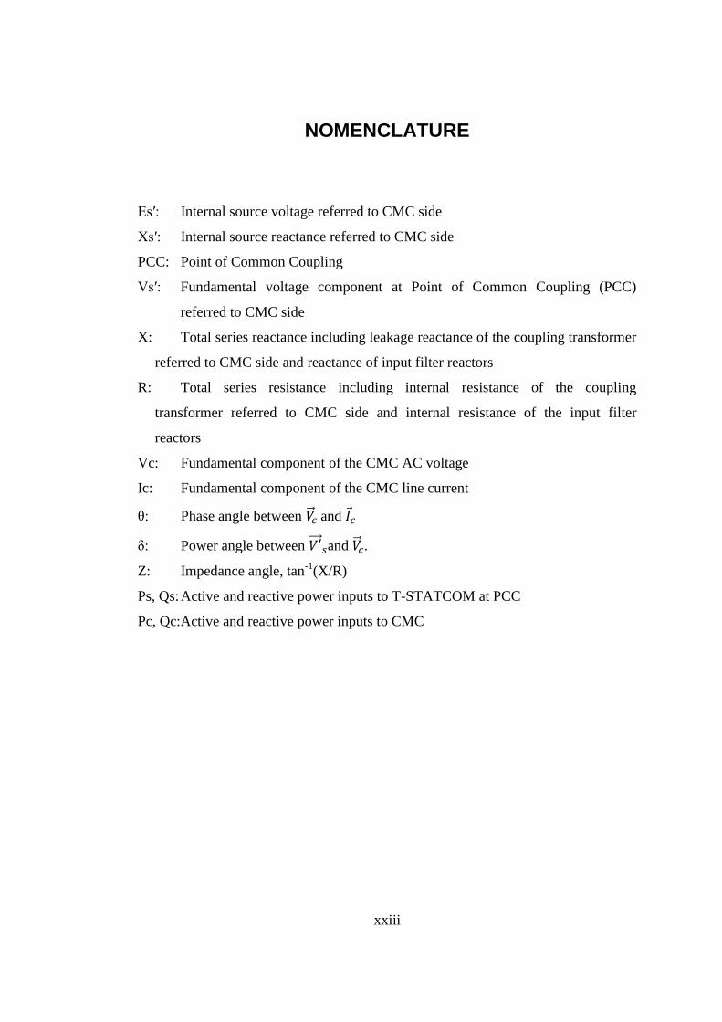
Figure 1.2 A practical SVC System [2]
application of an SVC system composed of Thyristor Controlled Reactor (TCR) and
fixed capacitor banks installed by TUBITAK-UZAY Power Electronics Department
for reactive power compensation of a ladle furnace.
The concept of STATCOM employing turn-off-capability semiconductor based
power converters instead of the use of inductor or capacitor banks for VAr
generation was firstly disclosed by Gyugyi [3]. In view of reactive power operation,
STATCOM systems look like Synchronous Condensers (SC) connected to the power
grids. SC is in fact a synchronous generator operating at no load. By changing field
current of the machine, the reactive power generated/absorbed is changed. If SC is
over-excited by the field current, it generates capacitive reactive power while it is
under-excited, it absorbs inductive reactive power. The major drawback of SCs is
their relatively slow transient response against rapid load changes. STATCOM may
give instant response to the rapidly changes of the power grid thanks to their power
converters. Unlike SVCs, their reactive power capability is independent from the
supply voltage variations and by switching power converters appropriately; reactive
power is manipulated for both capacitive and inductive operating regions. The V-I
4
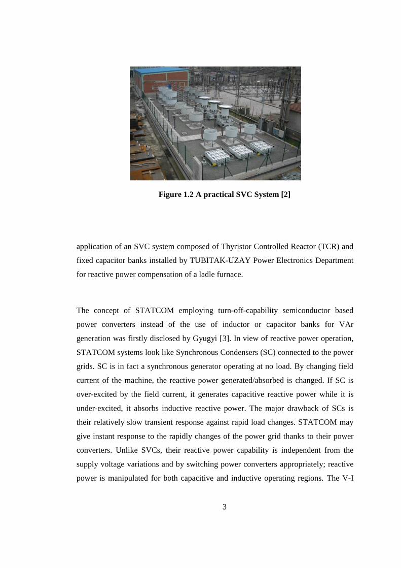
characteristics of STATCOM and a practical Distribution type STATCOM (D-
STATCOM) system are shown in Figure 1.3 and Figure 1.4, respectively.
Figure 1.3 V-I characteristic of STATCOM systems (Vs, Icap and Iind are supply
voltage, STATCOM capacitive and inductive currents, respectively)
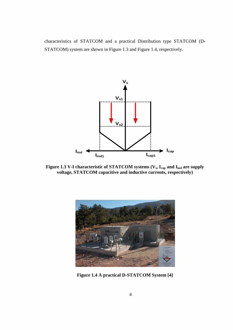
Figure 1.4 A practical D-STATCOM System [4]
Icap
Icap1
IindIind1
Vs
Vs1
Vs2
5
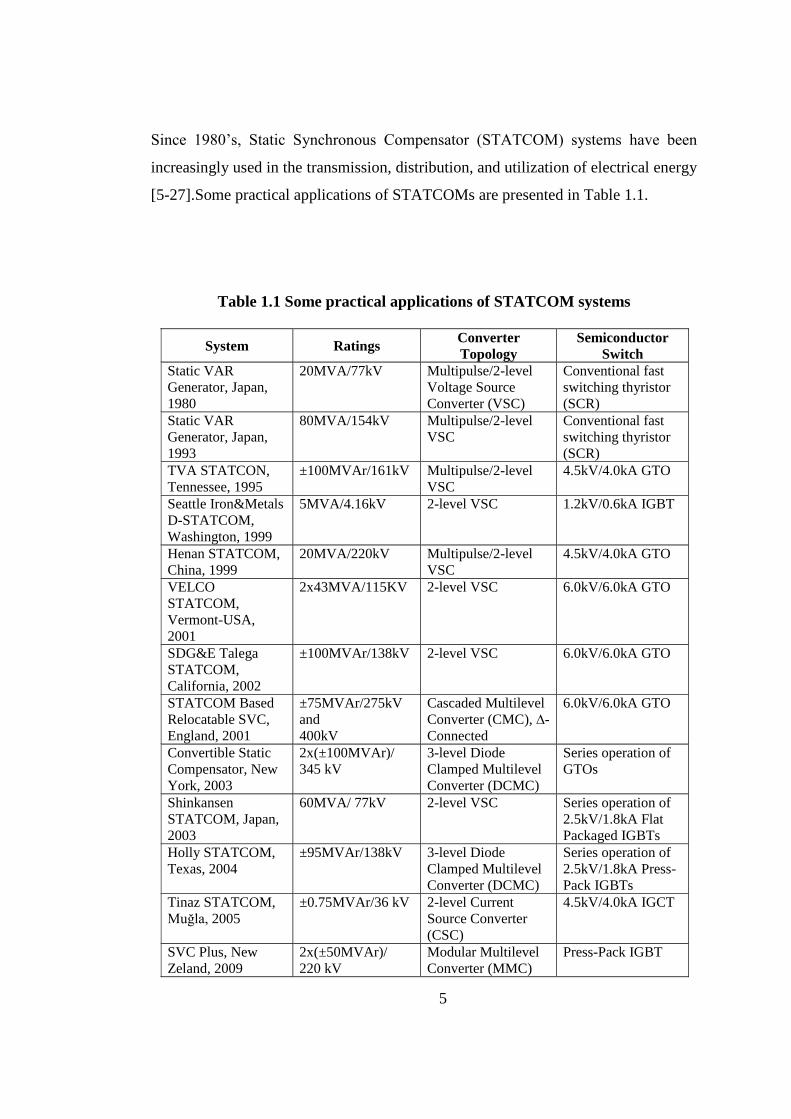
Since 1980’s, Static Synchronous Compensator (STATCOM) systems have been
increasingly used in the transmission, distribution, and utilization of electrical energy
[5-27].Some practical applications of STATCOMs are presented in Table 1.1.
Table 1.1 Some practical applications of STATCOM systems
System Ratings Converter
Topology
Semiconductor
Switch
Static VAR
Generator, Japan,
1980
20MVA/77kV Multipulse/2-level
Voltage Source
Converter (VSC)
Conventional fast
switching thyristor
(SCR)
Static VAR
Generator, Japan,
1993
80MVA/154kV Multipulse/2-level
VSC
Conventional fast
switching thyristor
(SCR)
TVA STATCON,
Tennessee, 1995
±100MVAr/161kV Multipulse/2-level
VSC
4.5kV/4.0kA GTO
Seattle Iron&Metals
D-STATCOM,
Washington, 1999
5MVA/4.16kV 2-level VSC 1.2kV/0.6kA IGBT
Henan STATCOM,
China, 1999
20MVA/220kV Multipulse/2-level
VSC
4.5kV/4.0kA GTO
VELCO
STATCOM,
Vermont-USA,
2001
2x43MVA/115KV 2-level VSC 6.0kV/6.0kA GTO
SDG&E Talega
STATCOM,
California, 2002
±100MVAr/138kV 2-level VSC 6.0kV/6.0kA GTO
STATCOM Based
Relocatable SVC,
England, 2001
±75MVAr/275kV
and
400kV
Cascaded Multilevel
Converter (CMC), ∆-
Connected
6.0kV/6.0kA GTO
Convertible Static
Compensator, New
York, 2003
2x(±100MVAr)/
345 kV
3-level Diode
Clamped Multilevel
Converter (DCMC)
Series operation of
GTOs
Shinkansen
STATCOM, Japan,
2003
60MVA/ 77kV 2-level VSC Series operation of
2.5kV/1.8kA Flat
Packaged IGBTs
Holly STATCOM,
Texas, 2004
±95MVAr/138kV 3-level Diode
Clamped Multilevel
Converter (DCMC)
Series operation of
2.5kV/1.8kA Press-
Pack IGBTs
Tinaz STATCOM,
Muğla, 2005
±0.75MVAr/36 kV 2-level Current
Source Converter
(CSC)
4.5kV/4.0kA IGCT
SVC Plus, New
Zeland, 2009
2x(±50MVAr)/
220 kV
Modular Multilevel
Converter (MMC)
Press-Pack IGBT
6
In these practical STATCOM systems implemented in the field, various power
semiconductors have been employed i.e., silicon-controlled rectifiers (conventional
fast switching thyristors) [5], Gate Turn-off thyristors (GTO) [6,7,9-11,14], Insulated
Gate Bipolar Transistors (IGBT) [8,12,13,15,16,19-22,26,27], Injection Enhanced
Insulated Gate Transistor (IEGT) [15] and Integrated Gate Commutated Thyristors
(IGCT) [18,23-25]. Two-level, six-pulse bridge converters with relatively high
switching frequencies and relatively low installed capacities are usually being the
characteristics of Distribution type STATCOM (D-STATCOM) systems [18, 23-25].
These are usually connected to the Medium Voltage (MV) load bus via a step-up
coupling transformer. However, Transmission type STATCOM (T-STATCOM)
systems have much higher installed capacities and therefore the power
semiconductors in their converter system/s should be switched at lower frequencies.
That is why in practical applications of T-STATCOM systems either multi-pulse
converters based on two-level six-pulse bridge [5-7,9,15] or three-level Neutral Point
Clamped (NPC) [17] converters with inter-magnetics or Multilevel Converter (MC)s
[10-14,16,18,19-21] are to be utilized. Cascaded Multilevel Converter (CMC)s
[12,20-22], and Diode Clamped Multilevel Converter (DCMC)s
[10,11,13,14,16,18,19] are generally employed in field prototypes or commercial
types of T-STATCOM applications. These systems are connected to the High
Voltage (HV) or extra high voltage (EHV) buses of the transmission systems via
coupling transformers.
Various topologies, modulation methods, control techniques and application areas of
MCs are reviewed in [28-33]. In literature, Multilevel Converters for T-STATCOM
applications are classified in three groups:
a) Diode Clamped Multilevel Converters (DCMC),
b) Flying Capacitor Multilevel Converters (FCMC),
c) Cascaded Multilevel Converters (CMC).
7
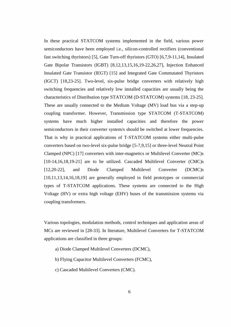
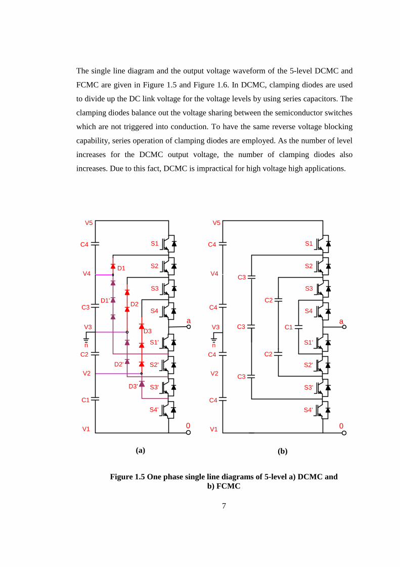
The single line diagram and the output voltage waveform of the 5-level DCMC and
FCMC are given in Figure 1.5 and Figure 1.6. In DCMC, clamping diodes are used
to divide up the DC link voltage for the voltage levels by using series capacitors. The
clamping diodes balance out the voltage sharing between the semiconductor switches
which are not triggered into conduction. To have the same reverse voltage blocking
capability, series operation of clamping diodes are employed. As the number of level
increases for the DCMC output voltage, the number of clamping diodes also
increases. Due to this fact, DCMC is impractical for high voltage high applications.
(a)
(b)
Figure 1.5 One phase single line diagrams of 5-level a) DCMC and
b) FCMC
S1
S2
S3
S4
S1'
S2'
S3'
S4'
D1
D2
D3
D1'
D2'
D3'
V5
V4
V3
V2
V1
a
0
n
C4
C3
C2
C1
S1
S2
S3
S4
S1'
S2'
S3'
S4'
C1
V5
V4
V3
V2
V1
a
0
n
C4
C4
C4
C4
C2
C2
C3
C3
C3
8
Figure 1.6 The output voltage waveform of 5-level
DCMC and 5-level FCMC
In FCMC, instead of clamping diodes in DCMC, clamping capacitors are used in
addition to the main DC link capacitors to obtain a staircase output voltage waveform
shown by Figure 1.6. By using proper clamping capacitor combinations, it is possible
to control the charging of clamping capacitors. As the number of level increases, the
number of clamping capacitors increases as well.
To obtain 5-level output voltage waveform shown in Figure 1.6, two series
connected H-Bridge (HB) circuits as shown in Figure 1.7 are used. The multilevel
converter topology based on the series connection of HBs is called Cascaded
Multilevel Converter (CMC). Since CMC topology is based on H-Bridge (HB)
circuits connected in series, it has the advantage of modularity and flexibility.
Modularized circuit layout and packaging is possible due to the usage of the same
structure for each level and there is no need to use clamping diodes or capacitors
required for DCMC and FCMC. The modular structure also gives the opportunity to
adjust the number of output voltage levels easily by changing only the number of
HBs in series.
wt
V5
Van
V4
V2
V1
V3

9
The comparison of M-level DCMC, FCMC and CMC is given in Table 1.2 in
accordance with the number of total power components needed for 3-phase
application. The voltage ratings of the devices are taken as equal to have a fair
comparison among the converter topologies.
Figure 1.7 One phase single diagram of 5-level CMC
Table 1.2 The total number of required power components
for M-level DCMC, FCMC and CMC
Although it requires more main DC link capacitors, the least number of needed
power components is achieved by the utilization of M-level CMC as can be seen
from Table 1.2. A very high amount of the total capacitance is required for the
Vout
+Vdc1
Vdc2
a
n
S1
S2
S3
S4
S1
S2
S3
S4
M-level Converter Topology
Converter Type DCMC FCMC CMC
Number of Switching Device 3x2x(M-1) 3x2x(M-1) 3x2x(M-1)
Number of DC Link Capacitors M-1 M-1 3x(M-1)/2
Number of Clamping Diodes 3x(M-1)x(M-2) 0 0
Number of Clamping Capacitors 0 3x(M-1)x(M-2)/2 0
10
FCMC topology. This is unacceptable for high voltage levels due to the equalization
problem of capacitors as well as the high cost. In DCMC topology with higher levels
than three-level configuration, oversized capacitors or complex balancing circuits
and methods should be employed in high voltage-high power applications for the
equalization problem of DC link capacitors. The usage of series connected clamping
diodes also yields the need of voltage sharing circuits which complicates the
packaging of practical applications. Due to its modularity, flexibility and less number
of power components, CMC topology is the most promising alternative for T-
STATCOM applications among the multilevel converters. It is possible to reach high
voltage levels by the use of more HBs in series for CMC topology. The only problem
is the balancing of the individual DC link capacitor voltages of each HB. This
problem can be overcome by employing some equalization methods.
The major operational problem of CMCs is the equalization of DC link capacitor
voltages. The equalization of DC link capacitor voltages are investigated and some
novel strategies are recommended in [34-52] for various CMC topologies.
Commercial CMC-based T-STATCOMs employ either GTO or GCT/IGCT devices
with inverse-parallel connected power diodes. To limit di/dt overvoltages on GTOs
during turn-off operation, bulky snubber circuits were used [12]. To equalize
individual capacitor voltages, high frequency IGBT based auxiliary circuits supplied
from low voltage side were employed. Specially designed isolating transformers
were used to isolate auxiliary circuits from the power stage of CMC.
An important contribution to the solution of voltage equalization problem of DC link
capacitors is known as the Selective Swapping Algorithm [50-52] which can be
embedded in the control algorithm of CMC, thus eliminating the need for bulky
auxiliary circuits. Although the effectiveness of voltage equalization algorithm
decreases as the number of H-bridges connected in series and/or peak-to-peak ripple
content of the capacitor voltage increase/s, it provides the lowest switching
frequency for the power semiconductors.
11
1.2 Scope of the Thesis
This research and technology development work deals with the sizing, system and
power-stage designs of an HV IGBT based CMC for T-STATCOM applications.
System design and the number of H-Bridge (HB)s in each phase of the Y-connected
CMC are achieved in view of Total Harmonic Distortion (THD) at Point of Common
Coupling (PCC), and also of Total Demand Distortion (TDD) of the line currents
and individual harmonic current limits recommended by IEEE Std.519-1992. A 12
kV, ±10 MVAr, 11-level CMC Module power stage with five HBs in each phase is
designed and then implemented to deliver ±10MVAr to 154kV transmission bus
(PCC) via a series filter reactor and 154/10.5kV coupling transformer. Therefore, the
CMC Module presented in this work constitutes the building block of large T-
STATCOM systems. The Selective Harmonic Elimination Method (SHEM) is
applied to synthesize T-STATCOM voltage waveforms at power frequency (50Hz)
and the Modified Selective Swapping (MSS) Algorithm is exercised to balance the
DC link capacitor voltages, perfectly at the expense of higher switching frequency,
and hence switching losses. The power stage is carefully designed and its
performance is optimized in view of the current HV IGBT technology.
A 154kV, ±50 MVAr, 11-level T-STATCOM system by the parallel use of five
CMCs built in this work has been implemented in the field primarily for the purposes
of reactive power compensation and terminal voltage regulation, and secondarily for
power system stability. Since the operating voltage of CMC is chosen to be 10.5 kV
(max.12 kV) line-to-line, it is connected to 154 kV line-to-line transmission bus
through a specially designed 50/62.5 MVA Y-Y connected (YNyn vector group)
coupling transformer and each CMC module is connected to the secondary side of
the coupling transformer via a series filter reactor bank.
This research work has made the following original contributions to the area of
Cascaded Multilevel Converter based Transmission STATCOM Systems:
12
Optimized design for the sizing, system and power stage of Cascaded
Multilevel Converter based T-STATCOM systems has been investigated.
A 12kV, ±10MVAr HV IGBT based CMC has been designed and implemented
as a building block of large T-STATCOM systems. Then, a 154kV, ±50MVAr
Transmission STATCOM system based on five of this CMC is implemented in
the field for the purposes of reactive power compensation and terminal voltage
regulation as well as power stability improvement [21].
The effect of total series inductance on system design has been investigated in
details.
The Conventional Selective Swapping (CSS) Method has been modified and
the effect of swapping time on the system performance has been exercised. The
comparison of Conventional and Modified Selective Swapping Algorithms has
also been presented by the computer simulations and field results.
The switching strategies have been discussed for Selective Swapping Methods
and alternatives for eliminating or reducing the voltage spikes as a result of
swappings have also been declared.
This is the first application of CMC based T-STATCOM with wire-bond HV
IGBTs and Modified Selective Swapping (MSS) Algorithm in the world.
Thanks to MSS method, the usage of bulky auxiliary circuits for equalization of
the DC link voltages has been eliminated and a compact H-Bridge (HB) unit
has been designed and implemented.
The outline of the thesis is given below:
In Chapter 2, operation principles of the Cascaded Multilevel Converter based T-
STATCOM systems have been discussed in detail. Active and Reactive power
control with waveform synthesizing used for STATCOM systems are clearly
presented. Moreover, the methods proposed in the literature for the equalization
13
problem of DC link capacitors used for CMCs have been reviewed with the details of
the Modified Selective Swapping Algorithm.
Chapter 3 presents the system design and sizing for CMC and T-STATCOM
systems. The major considerations for determining the connection point of T-
STATCOM systems are given in view of Total Harmonic Distortion (THD) at Point
of Common Coupling (PCC), Total Demand Distortion (TDD) of the line currents
and individual harmonic current limits recommended by IEEE Std.519- 1992. Also,
the effect of total series inductance on the system performance has been investigated
in detail.
The design issues including HB circuit, control system and switching strategies for
the application of selective swapping methods for Cascaded Multilevel Converters
have been presented in Chapter 4. The choice of power semiconductors and
capacitors used in each HB are given with the design details of the laminated busbar
with 3-conducting layer.
In Chapter 5, the system implementation with the field performance results have
been demonstrated. The waveforms and technical results of the system performance
have been given.
Conclusions and recommendations for the future work are given in Chapter 6. All the
theoretical and practical considerations of the thesis study is justified and concluded
in this chapter once more.

14
CHAPTER 2
OPERATING PRINCIPLES OF CMC BASED
TRANSMISSION STATCOM
2.1 System Description
Figure 2.1 shows single line diagram of a Transmission type Static Synchronous
Compensator (T-STATCOM) based on a single Cascaded Multilevel Converter
(CMC). It is shown to be connected to Extra High Voltage (EHV) or High Voltage
(HV) busbar of the transmission system via a medium voltage (MV) to EHV or HV
coupling transformer. Therefore, in Figure 2.1, Xr represents the total leakage
reactance of
Figure 2.1 Single line diagram of a T-STATCOM based on a single CMC
400 kV or
154 kV Bus
v’s vci jXr
vd1
iC1
+
C1
+
C2
+
Cn
vd1
vc iv’s iiC1
jXs
e’s
MV Bus
15
the coupling transformer and if needed the reactance of the series filter reactor.
Waveforms of EHV or HV bus voltage, vs’, line current of T-STATCOM, i, AC
voltage of the CMC, vc, voltage of each DC link capacitor, vd1 , and the current
through each DC link capacitor, iC1 are also sketched on Figure 2.1. es’, Xs’ and vs’
are respectively internal source voltage, source reactance and EHV or HV bus
voltage all referred to the CMC side.
Circuit diagram of star-connected CMC consisting of n number of series connected
H-Bridges (HBs) in each phase is as shown in Figure 2.2. n seriesly connected H-
Bridges give l=2n+1 steps in line-to-neutral voltage waveforms and l=4n+1 steps in
line-to-line voltage waveforms, where l is the number of levels from positive peak to
negative peak of the waveform under consideration. The DC link of each HB in the
CMC is equipped with a DC/DC converter controlled discharge resistor (R) to
discharge C when the CMC is disconnected from the supply for inspection or
maintenance purpose. Lr is the equivalent inductance of the total filter reactance, Xr,
in Figure 2.1. A T-STATCOM system operates at power frequency (50Hz or 60Hz)
as a shunt connected Flexible AC Transmission System (FACTS) device and
performs one or more than one of the following functions at the EHV or HV bus to
which the T-STATCOM is connected:
a. Terminal Voltage Regulation
b. Control of Reactive Power Flow in O/H Lines
c. Power System Stability Improvement
These are achieved by continuously varying the reactive power generated by the T-
STATCOM in both capacitive and inductive regions as will be described in the
forgoing sections.

16
N
Vsa
R+
Ca
1
R+
Cb
1R
+
Cc
1
R+
Ca2
R+
Ca
n
R+
Cb
2
R+
Cb
n
R+
Cc2
R+
Cc
n
Vca
Vsb
Vcb
Vsc
Vcc
Lr Lr Lr
Figure 2.2 Circuit diagram of a star-connected CMC consisting of n series
connected HBs in each phase
2.2 Active and Reactive Power Control
Single-phase Y-equivalent circuit model of the T-STATCOM and its phasor diagram
are given in respectively in Figure 2.3 and Figure 2.4, where:
Es′: Internal source voltage referred to CMC side
Xs′: Internal source reactance referred to CMC side
PCC: Point of Common Coupling
Vs′: Fundamental voltage component at Point of Common Coupling (PCC)
referred to CMC side
X: Total series reactance including leakage reactance of the coupling transformer
referred to CMC side and reactance of input filter reactors
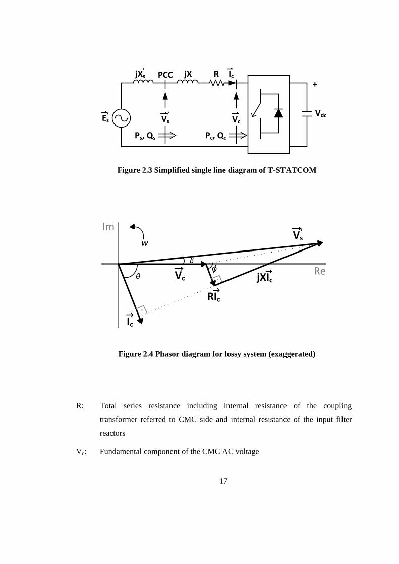
17
Figure 2.3 Simplified single line diagram of T-STATCOM
Figure 2.4 Phasor diagram for lossy system (exaggerated)
R: Total series resistance including internal resistance of the coupling
transformer referred to CMC side and internal resistance of the input filter
reactors
Vc: Fundamental component of the CMC AC voltage
Vdc
PCC+
R
Ps, Qs
jX
Es Vc
jXs
Vs
Pc, Qc
Ic
θ
Ic
δ
Re
Im
jXIc
RIc
Vc
wVs
18
Ic: Fundamental component of the CMC line current
θ: Phase angle between and
δ: Power angle between and
: Impedance angle, tan-1
(X/R)
Ps, Qs: Active and reactive power inputs to T-STATCOM at PCC
Pc, Qc: Active and reactive power inputs to CMC
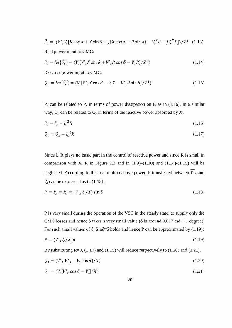
The definitions of θ and δ are expressed by the aid of Figure 2.5.
Figure 2.5 The definitions of δ and θ
In Figure 2.4, all voltages and currents are fundamental values and active and
reactive powers are per phase values. Ps, Pc, Qs and Qc in Figure 2.3 can be expressed
respectively as in (1.1)-(1.4), in terms of terminal quantities Vs′ and Vc and angles θ
and δ without consideration of harmonic components due to their negligible effects.
5Vd
π/20
π
3π/2 2π
vca
v'sa
-5Vd
δ
ia
θ

19
(1.1)
(1.2)
(1.3)
(1.4)
Since
;
T-STATCOM Current is . (1.5)
Complex power input to T-STATCOM:
(1.6)
(1.7)
Multiplying numerator and denominator by (R+jX):
(1.8)
where, Z = √(R2+X
2).
Real power input to T-STATCOM:
(1.9)
Reactive power input to T-STATCOM:
(1.10)
Complex power input to CMC:
(1.11)
(1.12)
Multiplying numerator and denominator by (R+jX):
20
(1.13)
Real power input to CMC:
(1.14)
Reactive power input to CMC:
(1.15)
Pc can be related to Ps in terms of power dissipation on R as in (1.16). In a similar
way, Qc can be related to Qs in terms of the reactive power absorbed by X.
(1.16)
(1.17)
Since Ic2R plays no basic part in the control of reactive power and since R is small in
comparison with X, R in Figure 2.3 and in (1.9)–(1.10) and (1.14)-(1.15) will be
neglected. According to this assumption active power, P transferred between and
can be expressed as in (1.18).
(1.18)
P is very small during the operation of the VSC in the steady state, to supply only the
CMC losses and hence δ takes a very small value (δ is around 0.017 rad ≡ 1 degree).
For such small values of δ, Sinδ≈δ holds and hence P can be approximated by (1.19):
(1.19)
By substituting R=0, (1.10) and (1.15) will reduce respectively to (1.20) and (1.21).
(1.20)
(1.21)

21
Since δ is very small, Cosδ≈1 holds. Hence (1.20) and (1.21) can be approximated to
(1.22) and (1.23), respectively.
(1.22)
(1.23)
Complex power input, to the T-STATCOM is defined according to
power sink convention. P is always positive in the steady-state to compensate for
coupling transformer, series filter reactor and CMC losses. However, the sign of Qs
depends upon the operation mode of the T-STATCOM, i.e. positive for inductive
mode of operation and negative for capacitive mode. θ is positive (≈+π/2) for
inductive mode of operation in the steady state while it is negative (≈-π/2) for
capacitive mode. The transition between capacitive and inductive mode of operations
occurs when , which corresponds to unity power factor (pf) operation of
the T-STATCOM at PCC.
Active power into the T-STATCOM is controlled by varying δ in order to keep the
DC link capacitor voltages constant at a pre-specified value over the entire operating
range in both transient-state and steady-state. δ is always positive in the steady-state
under the assumption of R=0. However, δ may have negative values for inductive
operation mode of the T-STATCOM (Vs′ > Vc) when R is not neglected. This occurs
for very small values of δ and even for a practical X/R ratio. This phenomenon is
apparent from (1.9) and (1.14). This small negative value for δ does not reverse the
direction of real power flow for the operation of the system given in Figure 2.3 in the
steady-state. For capacitive operation mode however, since Vs′ < Vc; δ is always
positive as can be understood from (1.9) and (1.14).
22
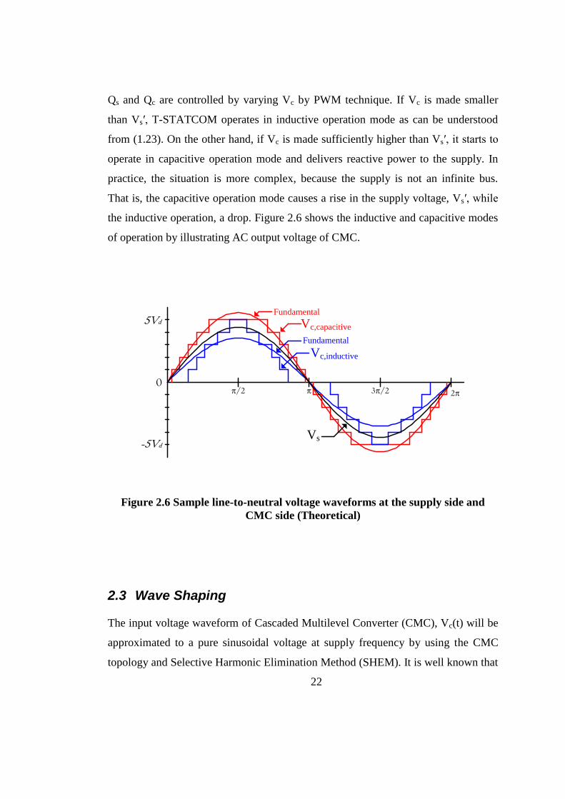
Qs and Qc are controlled by varying Vc by PWM technique. If Vc is made smaller
than Vs′, T-STATCOM operates in inductive operation mode as can be understood
from (1.23). On the other hand, if Vc is made sufficiently higher than Vs′, it starts to
operate in capacitive operation mode and delivers reactive power to the supply. In
practice, the situation is more complex, because the supply is not an infinite bus.
That is, the capacitive operation mode causes a rise in the supply voltage, Vs′, while
the inductive operation, a drop. Figure 2.6 shows the inductive and capacitive modes
of operation by illustrating AC output voltage of CMC.
Figure 2.6 Sample line-to-neutral voltage waveforms at the supply side and
CMC side (Theoretical)
2.3 Wave Shaping
The input voltage waveform of Cascaded Multilevel Converter (CMC), Vc(t) will be
approximated to a pure sinusoidal voltage at supply frequency by using the CMC
topology and Selective Harmonic Elimination Method (SHEM). It is well known that
5Vd
π/20
π 3π/2 2π
Fundamental
Vc,capacitive
-5Vd
Fundamental
Vc,inductive
Vs

23
the number of voltage levels, l, in the staircase voltage waveform in Figure 2.2
produced by CMC is defined by (1.24) and (1.25):
l=2n+1 in the line-to-neutral voltage (1.24)
l=4n+1 in the line-to-line voltage (1.25)
where, n is the number of HBs in one phase. As an example, in the CMC described
in this work, five HBs are connected in series in each phase to form a Y-connected
multilevel converter topology. This CMC yields 11 voltage levels in the line-to-
neutral voltage waveform and 21 voltage levels in the line-to-line voltage waveform.
The use of n number of HBs in each phase provides us n number of freedom in the
application of SHEM as can be seen in Appendix-A for CMC having 5 HBs in series.
One of them is allocated to the fundamental component while n-1 is for the
elimination of low order harmonics. For a star-connected CMC, the number of steps
in line-to-neutral voltage waveforms (l=2n+1), the number of steps in line-to-line
voltage waveforms (l=4n+1), and the odd harmonics that will be eliminated in line-
to-neutral voltage waveforms by SHEM are given in Table 2.1 as a function of
number of HBs, n in each phase. The optimum angles θ1,θ2,…,θn in [21],[48] which
define starting and end points of each pulse in the staircase line-to-neutral voltage
waveform of CMC to give minimum harmonic content and hence minimum THD
values are calculated off-line by using a hybrid algorithm . The hybrid algorithm is a
combination of the genetic algorithm [49], [53] and the gradient based method. First,
the genetic algorithm is used for determination of proper initial conditions. Then,
these initial conditions are applied to the gradient based method to reach the global
minima much faster than the use of genetic algorithm only. These calculations are
repeated several times for different modulation indices, M, to cover the whole
operating range of the CMC and then stored in a look-up table as described in [21].
Optimum values of θ1,θ2,...,θn are obtained for different modulation index values so
that -Q MVAr to +Q MVAr reactive power control range is divided into N steps and

24
corresponding results are arranged as a Nx6 Look-up Table. The hybrid algorithm is
applied for CMC with three, five and seven HBs to obtain optimum angles with
respect to M values to give minimum THD value of line-to-neutral voltages. The
obtained M ranges are [2.50-4.23], [1.15-2.52] and [3.26-5.73] with 0.01 resolution
for CMC with three, five and seven HBs, respectively. Some sample results of
optimum angles with respect to modulation index value, M for mentioned topologies
are given Table 2.2 - Table 2.4. As can be seen from Table 2.4 for CMC having
seven HBs, there are no solution for optimum angles corresponding to the M ranges
of [5.14-5.17] and [5.43-5.55].
Table 2.1 Number of steps in CMC AC voltages and low order voltage
harmonics eliminated as a function of number of HBs
Number of
HBs, n
Number of steps in voltage l-to-n voltage harmonics
eliminated, n-1 l-to-n,l=2n+1 l-to-l,l=4n+1
3 7 13 5th
, 7th
5 11 21 5th
, 7th
, 11th
, 13th
7 15 29 5th
, 7th
, 11th
, 13th
, 17th
, 19th
Table 2.2 Optimum angles with respect to
modulation index values for CMC having 3HBs
M θ1(rad) θ2(rad) θ3(rad)
1.15 0.717 1.165 1.570
1.16 0.715 1.159 1.566
1.17 0.713 1.153 1.563
... ... ... ...
2.50 0.239 0.375 0.930
2.51 0.252 0.356 0.922
2.52 0.273 0.327 0.915

25
As illustrated in Figure 2.7, five pulses with different widths and the same
magnitudes (Vd) are to be superimposed in order to create a half-cycle of an 11-level
line-to-neutral voltage waveform. This makes necessary assigning five different
Table 2.3 Optimum angles with respect to
modulation index values for CMC having 5HBs
M θ1(rad) θ2(rad) θ3(rad) θ4(rad) θ5(rad)
2.50 0.620 0.794 0.998 1.208 1.482
2.51 0.621 0.792 0.997 1.204 1.478
2.52 0.621 0.790 0.996 1.200 1.474
... ... ... ... ... ...
4.21 0.121 0.249 0.414 0.641 1.010
4.22 0.135 0.231 0.418 0.632 1.006
4.23 0.160 0.203 0.423 0.623 1.002
Table 2.4 Optimum angles with respect to
modulation index values for CMC having 7HBs
M θ1(rad) θ2(rad) θ3(rad) θ4(rad) θ5(rad) θ6(rad) θ7(rad)
3.26 0.592 0.735 0.877 1.033 1.199 1.397 1.571
3.27 0.591 0.735 0.876 1.032 1.196 1.393 1.569
3.28 0.591 0.734 0.875 1.030 1.194 1.390 1.568
... ... ... ... ... ... ... ...
5.14
No solution for optimum angles ...
5.17
5.18 0.156 0.334 0.446 0.653 0.890 1.014 1.167
... ... ... ... ... ... ... ...
5.43
No solution for optimum angles ...
5.55
... ... ... ... ... ... ... ...
5.71 0.077 0.243 0.313 0.469 0.626 0.885 1.098
5.72 0.072 0.248 0.305 0.469 0.621 0.880 1.096
5.73 0.067 0.256 0.293 0.469 0.615 0.876 1.095

26
angles θ1,θ2,…,θ5 in such a way that the harmonic distortion of line-to-neutral
voltage waveform will be minimum. 3rd
harmonic and its integer multiples will not
appear in the line-to-line voltage waveform. There remains only the elimination of
dominant voltage harmonics which are the 5th
, 7th
, 11th
and 13th
. In a staircase
waveform with odd-quarter symmetry, these are eliminated by using SHEM in the
work. If a lower harmonic content were allowed in line-to-line voltage waveform, a
larger series filter reactor would be needed at the expense of voltage regulation
problem.
Figure 2.7 11-level line-to-neutral voltage waveform [46]
The rms value of the fundamental component of CMC output voltage Vc can be
controlled by adjusting the modulation index, M according to (1.26)-(1.29):
5Vd
π/20
0π
3π/2
2π
-5Vd
Vd
0-Vd
Ea
Ea*
θ5
P5P5
P4P4
P3P3
P2P2
P1P1
π-θ5
π-θ4 θ4
θ3
θ2
θ1
π-θ3
π-θ2
π-θ1

27
Vc = Vc(ref) (1.26)
M = Vc(ref)/Vc(max) (1.27)
π (1.28)
Vd = (Vdc/n) (1.29)
where, Vc(ref) is the set value of fundamental line-to-line rms output voltage of the
CMC determined by the controller, Vc(max) denotes the maximum value of
fundamental line-to-line rms voltage of the quasi-square wave that can be produced
by an HB, Vd is the mean DC link voltage of each HB and Vdc is the total mean DC
link voltage of each CMC phase.
Since M has been defined with respect to the AC output voltage of each HB, the
above formulation yields M values greater than unity. As an example, for n=5 and
= ±10MVAr, M should be varied from 3.0 to 3.73 as will be described in
Chapter 3 in the prototype of T-STATCOM developed in this work. Some sample
results of EMTDC/PSCAD simulations carried out for a ±10MVAr, 10.5 kV CMC
under CSS method are shown in Figure 2.8 - Figure 2.9 for inductive and capacitive
operation modes, respectively. These waveforms show that 11-level line-to-neutral
voltage waveforms and 21-level line-to-line voltage waveforms are successfully
formed by the waveform synthesizing method used in this work. Morever, the line-
to-neutral voltage waveforms of the CMC with the output voltages of five HB units
in phase-A are shown in Figure 2.10 and Figure 2.11. A comparison of voltage
waveforms for capacitive mode of operation with those of inductive mode shows the
effects of M-control on the widths of all pulses and hence on the CMC output
voltage. The widths of the HB output voltages for capacitive operation mode are
wider than those for inductive operation mode. Therefore, by controlling the widths
of the HB output voltages, the required CMC output voltage is obtained for both
capacitive and inductive operation modes by M-control.
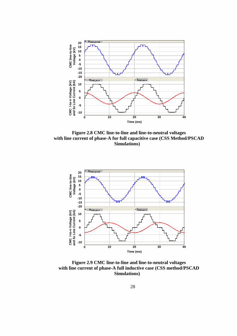
28
Figure 2.8 CMC line-to-line and line-to-neutral voltages
with line current of phase-A for full capacitive case (CSS Method/PSCAD
Simulations)
Figure 2.9 CMC line-to-line and line-to-neutral voltages
with line current of phase-A full inductive case (CSS method/PSCAD
Simulations)
ICMC,ph-A
VCMC,ph-AB
0 10 20 30 40
Time (ms)
-10
-5
0
5
10
20
15
10
5
0
-5
-10
-15
-20
CM
C lin
e-t
o-l
ine
Vo
lta
ge
(k
V)
VCMC,ph-A
CM
C l-
to-n
Vo
lta
ge
(k
V)
an
d 5
x L
ine
Cu
rre
nt
(kA
)
ICMC,ph-A
VCMC,ph-AB
0 10 20 30 40
Time (ms)
-10
-5
0
5
10
20
15
10
5
0
-5
-10
-15
-20
CM
C lin
e-t
o-l
ine
Vo
lta
ge
(k
V)
VCMC,ph-A
CM
C l-
to-n
Vo
lta
ge
(k
V)
an
d 5
x L
ine
Cu
rre
nt
(kA
)
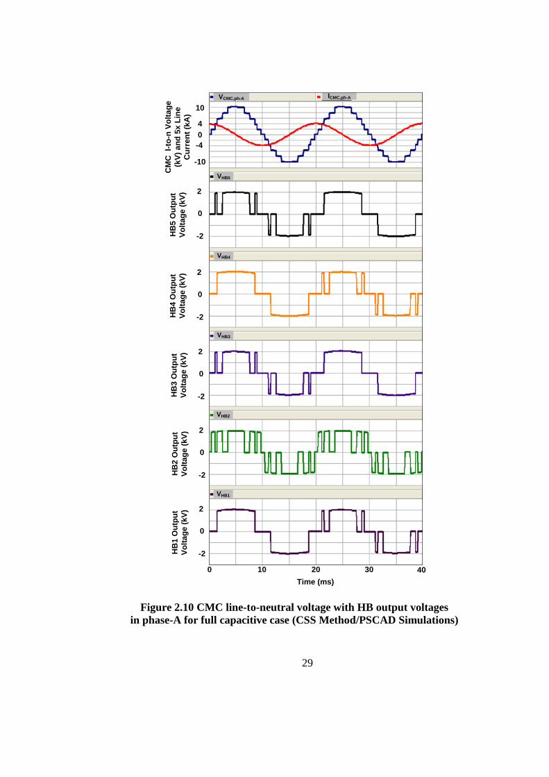
29
Figure 2.10 CMC line-to-neutral voltage with HB output voltages
in phase-A for full capacitive case (CSS Method/PSCAD Simulations)
Time (ms)
-10
-4
0
4
10
VCMC,ph-A ICMC,ph-A
VHB5
VHB4
VHB3
VHB2
VHB1
0 10 20 30 40
CM
C l-
to-n
Vo
lta
ge
(kV
) a
nd
5x
Lin
e
Cu
rre
nt
(kA
)2
0
-2HB
5 O
utp
ut
Vo
lta
ge
(k
V)
2
0
-2HB
4 O
utp
ut
Vo
lta
ge
(k
V)
2
0
-2HB
3 O
utp
ut
Vo
lta
ge
(k
V)
2
0
-2HB
2 O
utp
ut
Vo
lta
ge
(k
V)
2
0
-2HB
1 O
utp
ut
Vo
lta
ge
(k
V)

30
Figure 2.11 CMC line-to-neutral voltage with HB output voltages
in phase-A for full inductive case (CSS Method/PSCAD Simulations)
-10
-4
0
4
10
VCMC,ph-A ICMC,ph-A
VHB5
VHB4
VHB3
VHB2
VHB1
0 10 20 30 40
CM
C l-
to-n
Vo
lta
ge
(kV
) a
nd
5x
Lin
e
Cu
rre
nt
(kA
)2
0
-2HB
5 O
utp
ut
Vo
lta
ge
(k
V)
2
0
-2HB
4 O
utp
ut
Vo
lta
ge
(k
V)
2
0
-2HB
3 O
utp
ut
Vo
lta
ge
(k
V)
2
0
-2HB
2 O
utp
ut
Vo
lta
ge
(k
V)
2
0
-2HB
1 O
utp
ut
Vo
lta
ge
(k
V)
Time (ms)

31
2.4 Voltage Balancing of DC Link Capacitors
The major drawback of multilevel converters is the voltage balancing problem of DC
link capacitors [34-52]. For cascaded multilevel converters, there are many methods
proposed in the literature. In this work, the selective swapping method is modified
and then employed for the designed prototype of T-STATCOM system.
2.4.1 Some Conventional Methods
In [12], to equalize individual capacitor voltages, high frequency IGBT based
auxiliary circuits supplied from low voltage side were employed. Specially designed
isolating transformers were used to isolate auxiliary circuits from the power stage of
CMC. As a result, a bulky H-Bridge design were existed.
Figure 2.12 The α/∆α method for DC link capacitor balancing [48]

32
In order to equalize the capacitor voltages in each string, one of the conventional
methods adopted is to control the total DC capacitor voltage per phase by adjusting α
and individual DC capacitor voltages by shifting switching angles of each HB by an
amount of ±Δα [48] as shown in Figure 2.12.
The outer α control-loop is used for real power flow from supply to CMC to
compensate the related phase losses while the inner loop ±Δα control-loop is used to
shift the output voltage of each HB against line current to equalize the DC link
voltages. For M level CMC, there are numbers of inner loops to be
used for balancing and hence numbers of PI controllers should be used.
As the number of levels increases, the number of PI controllers also increases. This
yields control complexity since the corresponding PI parameters used to determine α
and Δα may be time-consuming, and difficult to find. Moreover, the PI controls of α
and Δα may interact with each other, resulting in instability.
Another conventional method proposed in [49] is to use α control only with just
measuring one DC link voltage as shown in Figure 2.13, and to rotate the switching
angles for HBs in every half-cycle as shown in Figure 2.14. The switching patterns
for the HBs are fixed during the half-cycle and they change in every half-cycle for
each HB. For M level CMC, the equalization for DC links is acheived after M half-
cycles of power frequency. Although, the advantage of this method to the α/Δα
proposed in [48] is no need for many inner control loops and hence PI controllers,
the duration for the equalization of DC link capacitors increases as the number of HB
increases, which may not be possible for fast changing loads.

33
Figure 2.13 The rotational angle method for DC link capacitor balancing [49]
Figure 2.14 The rotational of switching angles [49]

34
2.4.2 Conventional Selective Swapping (CSS) Method
An important contribution to the solution of voltage equalization problem of DC link
capacitors is known as the Selective Swapping Algorithm [50-51] which can be
embedded in the control algorithm of the CMC. This method is called the swapping
algorithm because at each level change (θ1 to θ5 in Figure 2.7), the previous set of
HB/s which are in operation is going to be interchanged with a new set in each phase
of each CMC module. It is called selective swapping algorithm because the swapping
operation is done according to the values of DC link capacitor voltages.
The method uses different redundant combinations of HBs at the instants of level
changes for DC link voltage balancing. The redundancy concept can be summarized
for a 7-level CMC as follows:
The method uses the redundancy combinations of HBs at each level changes of CMC
output voltage as shown in Figure 2.15 - Figure 2.17. As can be understood from the
Figure 2.15, for +3Vd and 0Vd levels, there is only one mode for these volatage
levels. Therefore, at these voltage levels, there is no any swapping operation due to
non-existence of a redundancy mode. Also, this is true for the -3Vd voltage level. At
+2Vd and +1Vd voltage levels, three different modes can be used as shown in Figure
2.16 and Figure 2.17. For example, from the transition from 0Vd to +1Vd level of
line-to-neutral voltage of CMC, one of Modes -1, -2 and -3 will be chosen. Also, for
the transition from +1Vd to +2Vd voltage level, one of three modes shown in Figure
2.17 will be used with at least one/at most two new incoming HBs. The choice of the
modes is determined by the charging or discharging states of the HBs as well as the
magnitudes of DC link capacitor voltages. The same conclusions can be drawn for -
1Vd and -2Vd voltage levels of CMC line-to-neutral voltages. That is respectively
three, three and one redundancy mode occur for -1Vd, -2Vd and -3Vd voltage levels.
Therefore, for a 7-level CMC, there are 15 modes (seven modes for positive voltage
levels, one mode for 0 level and seven modes for negative voltage levels) in total.
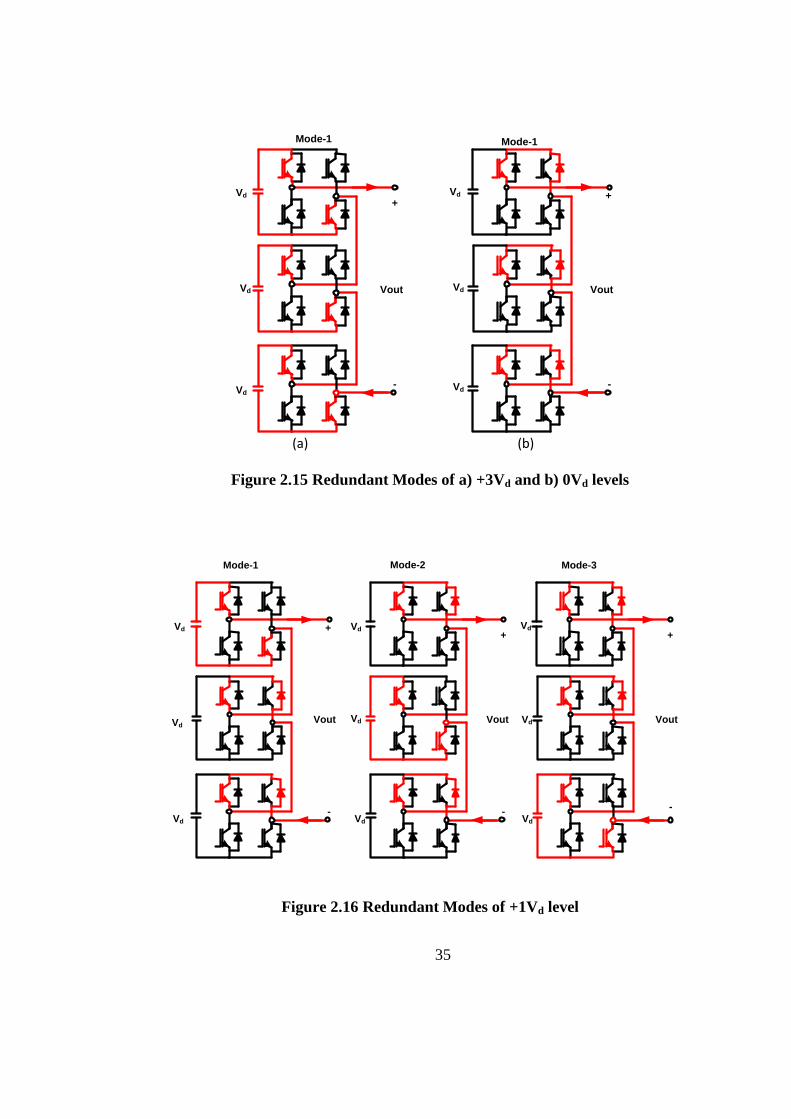
35
(a) (b)
Figure 2.15 Redundant Modes of a) +3Vd and b) 0Vd levels
Figure 2.16 Redundant Modes of +1Vd level
Vout
+
-
Vout
-
+Vd
Vd
VdVd
Vd
Vd
Mode-1 Mode-1
Vout
+
-
Vout
+
-
Vout
-
Vd +
Vd
Vd
Vd
Vd
Vd Vd
Vd
Vd
Mode-1 Mode-2 Mode-3

36
Figure 2.17 Redundant Modes of +2Vd level
The number of redundancy modes are directly proportional to the number of levels
for the CMC topology. For example for a 11-level CMC (n=5) and 15-level CMC
(n=7), the numbers of redundancy modes are shown in Table 2.5 and Table 2.6,
respectively.
Table 2.5 The number of redundancy modes for 11-level CMC
The Voltage Level Number of Redundancy Modes
0Vd 1
+1Vd,-1Vd 5,5
+2Vd,-2Vd 10,10
+3Vd,-3Vd 10,10
+4Vd,-4Vd 5,5
+5Vd,-5Vd 1,1
Total 63
Vout
+
-
Vout
+
-
Vout
+
-
Vd
Vd
Vd Vd
Vd
Vd Vd
Vd
Vd
Mode-1 Mode-2 Mode-3
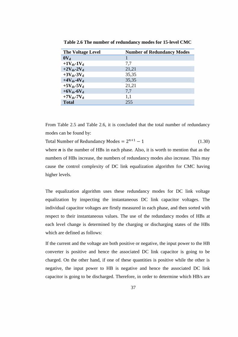
37
Table 2.6 The number of redundancy modes for 15-level CMC
The Voltage Level Number of Redundancy Modes
0Vd 1
+1Vd,-1Vd 7,7
+2Vd,-2Vd 21,21
+3Vd,-3Vd 35,35
+4Vd,-4Vd 35,35
+5Vd,-5Vd 21,21
+6Vd,-6Vd 7,7
+7Vd,-7Vd 1,1
Total 255
From Table 2.5 and Table 2.6, it is concluded that the total number of redundancy
modes can be found by:
(1.30)
where n is the number of HBs in each phase. Also, it is worth to mention that as the
numbers of HBs increase, the numbers of redundancy modes also increase. This may
cause the control complexity of DC link equalization algorithm for CMC having
higher levels.
The equalization algorithm uses these redundancy modes for DC link voltage
equalization by inspecting the instantaneous DC link capacitor voltages. The
individual capacitor voltages are firstly measured in each phase, and then sorted with
respect to their instantaneous values. The use of the redundancy modes of HBs at
each level change is determined by the charging or discharging states of the HBs
which are defined as follows:
If the current and the voltage are both positive or negative, the input power to the HB
converter is positive and hence the associated DC link capacitor is going to be
charged. On the other hand, if one of these quantities is positive while the other is
negative, the input power to HB is negative and hence the associated DC link
capacitor is going to be discharged. Therefore, in order to determine which HB/s are

38
going to be operated at each level change, the values of individual DC link capacitor
voltages, polarity of the HB output voltage and direction of the line current should be
measured.
The polarity of the output voltage to HBs is determined indirectly by using a PLL
circuit which is locked to line-to-neutral voltage at PCC. The digital signal produced
by PLL is phase advanced or delayed by power (load) angle, δ in Figure 2.5 to
determine the zero crossing point of the CMC module fundamental line-to-neutral
voltage. After determining the new status of DC link capacitors (charging or
discharging) by this way, HBs having the lowest DC link voltages will be put into
operation for charging and HBs having the highest DC link voltages, for discharging
mode of operations. This method is called the Conventional Selective Swapping
(CSS) in the work. The CSS gives minimum switching frequency for the power
semiconductors.
The CSS performance on the equalization of DC link capacitor voltages for a 12 kV,
±10MVAr, 11-level CMC having 9.2mF capacitance value for each HB has been
showed by the carried out computer simulations both for full inductive and
capacitive operation modes as given in Figure 2.18 - Figure 2.20. The individual DC
link voltages of five HBs in three phases of CMC for the case of full capacitive is
almost equal and circulates around 1900 V mean DC voltage as shown in Figure
2.18. However, the peak-to-peak ripple value of DC link voltage of HB1 in phase-A
of the CMC for inductive operation case is around 225V as shown in Figure 2.19
whereas those for capacitive operation mode is around 180V. The DC link voltages
of the 1st HBs in three phases are also almost equal as shown in Figure 2.20. These
results show that the CSS method is succesfull for the balancing of DC link voltages
of individual HBs in CMC in the expense of higher variations in peak-to-peak ripple
voltage.

39
(a)
(b)
(c)
Figure 2.18 The variations in the instantaneous DC link voltages of a) phase-A,
b) phase-B and c) phase-C HBs of 11-level CMC for full capacitive case
(PSCAD Simulations)
DC
Lin
k C
ap
ac
ito
r V
olt
ag
es
(V
)
1750
1775
1800
1825
1850
1875
1900
1925
1950
1975
2000
2025
0 100 200Time (ms)
Vd,1a Vd,2a Vd,3a Vd,4a Vd,5a
DC
Lin
k C
ap
ac
ito
r V
olt
ag
es
(V
)
1750
1775
1800
1825
1850
1875
1900
1925
1950
1975
2000
2025
0 100 200Time (ms)
Vd,1b Vd,2b Vd,3b Vd,4b Vd,5b
DC
Lin
k C
ap
ac
ito
r V
olt
ag
es
(V
)
1750
1775
1800
1825
1850
1875
1900
1925
1950
1975
2000
2025
0 100 200Time (ms)
Vd,1c Vd,2c Vd,3c Vd,4c Vd,5c

40
(a)
(b)
(c)
Figure 2.19 The variations in the instantaneous DC link voltages of a) phase-A,
b) phase-B and c) phase-C HBs of 11-level CMC for full inductive case (PSCAD
Simulations)
DC
Lin
k C
ap
ac
ito
r V
olt
ag
es
(V
)
1750
1775
1800
1825
1850
1875
1900
1925
1950
1975
2000
2025
0 100 200Time (ms)
Vd,1a Vd,2a Vd,3a Vd,4a Vd,5a
DC
Lin
k C
ap
ac
ito
r V
olt
ag
es
(V
)
1750
1775
1800
1825
1850
1875
1900
1925
1950
1975
2000
2025
0 100 200Time (ms)
Vd,1b Vd,2b Vd,3b Vd,4b Vd,5b
DC
Lin
k C
ap
ac
ito
r V
olt
ag
es
(V
)
1750
1775
1800
1825
1850
1875
1900
1925
1950
1975
2000
2025
0 100 200Time (ms)
Vd,1c Vd,2c Vd,3c Vd,4c Vd,5c

41
(a)
(b)
Figure 2.20 The variations in the instantaneous DC link voltages of 1st HBs in
three phases of 11-level CMC for a) full inductive, b) full capacitive cases
(PSCAD Simulations)
2.4.3 Modified Selective Swapping (MSS) Method
The major drawback of the CSS is the higher variations observed in the DC link
capacitor voltages as the number of HBs in each CMC is reduced. In order to
DC
Lin
k C
ap
ac
ito
r V
olt
ag
es
(V
)
1750
1775
1800
1825
1850
1875
1900
1925
1950
1975
2000
2025
0 100 200Time (ms)
Vd,1a Vd,1b Vd,1c
DC
Lin
k C
ap
ac
ito
r V
olt
ag
es
(V
)
1750
1775
1800
1825
1850
1875
1900
1925
1950
1975
2000
2025
0 100 200Time (ms)
Vd,1a Vd,1b Vd,1c

42
eliminate this drawback, the CSS is modified and then applied to T-STATCOM
described in the thesis. In the Modified Selective Swapping (MSS) algorithm,
selective swappings are applied not only at level changes but continuously at a pre-
specified frequency during the operation of the CMC. Figure 2.21 illustrates the
application of the MSS method proposed in the thesis in comparison with the CSS.
The only difference of MSS with CSS is the application of swappings for a specified
time not only the level changes but also during the levels. The flowchart of MSS
method proposed in the thesis is given in Figure 2.22.
Figure 2.21 The illustration of CSS and MSS
Some simulations are carrid out for a ±10MVAr CMC having five series HBs with
1900 V DC link voltages and 9.2mF capacitance values to compare the effects of
0
2
4
6
8
10
Line
-to-
Neu
tral
Vol
tage
(kV
)
CSS
t
MSS withΔts=400μs
Δts
MSS withΔts=200μs
Δts Δts Δts Δts
Δts
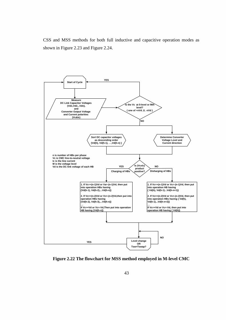
43
CSS and MSS methods for both full inductive and capacitive operation modes as
shown in Figure 2.23 and Figure 2.24.
Figure 2.22 The flowchart for MSS method employed in M-level CMC
Start of Cycle
Measure
DC Link Capacitor Voltages
(Vd1,Vd2,..Vdn),
and
Converter Output Voltage
and Current polarities
(Vc&Ic)
Sort DC capacitor voltages
as descending order
Vd(h), Vd(h-1), …,Vd(h-n)
Is (VcxIc)
product
positive?
YES NO
YES
NO
Level change
OR
Tsw=Tswap?
NO
YES
Is the Vc at 0-level or Mth
level?
( one of +nVd ,0, -nVd )
Charging of HBs Disharging of HBs
1. If Vc=+(n-1)Vd or Va=-(n-1)Vd, then put
into operation HBs having
Vd(h-1), Vd(h-2),...Vd(h-n)
2. If Vc=+(n-2)Vd or Vc=-(n-2)Vd,then put into
operation HBs having
Vd(h-2), Vd(h-3),...Vd(h-n)
…
If Vc=+Vd or Vc=-Vd,Then put into operation
HB having Vd(h-n)
n is number of HBs per phase
Vc is CMC line-to-neutral voltage
Ic is the line current
M is the voltage level
Vd is the DC link voltage of each HB
1. If Vc=+(n-1)Vd or Vc=-(n-1)Vd, then put
into operation HB having
Vd(h), Vd(h-1)...Vd(h-n+1)
2. If Vc=+(n-2)Vd or Vc=-(n-2)Vd, then put
into operation HBs having Vd(h),
Vd(h-1)...Vd(h-n+2)
…
If Vc=+Vd or Vc=-Vd, then put into
operation HB having Vd(h)
Determine Converter
Voltage Level and
Current direction

44
(a)
(b)
(c)
Figure 2.23 The variations in the instantaneous DC link voltages of the CMC
under a) CSS, b) MSS with ∆ts=400 µs and c) MSS with ∆ts=200 µs for full
capacitive case (PSCAD Simulations)
DC
Lin
k C
ap
ac
ito
r V
olt
ag
es
(V
)
1750
1775
1800
1825
1850
1875
1900
1925
1950
1975
2000
2025
0 100 200Time (ms)
Vd,1a Vd,2a Vd,3a Vd,4a Vd,5a
DC
Lin
k C
ap
ac
ito
r V
olt
ag
es
(V
)
1775
1800
1825
1850
1875
1900
1925
1950
1975
2000
0 100 200Time (ms)
Vd,1a Vd,2a Vd,3a Vd,4a Vd,5a
DC
Lin
k C
ap
ac
ito
r V
olt
ag
es
(V
)
1775
1800
1825
1850
1875
1900
1925
1950
1975
2000
0 100 200
Vd,1a Vd,2a Vd,3a Vd,4a Vd,5a
Time (ms)
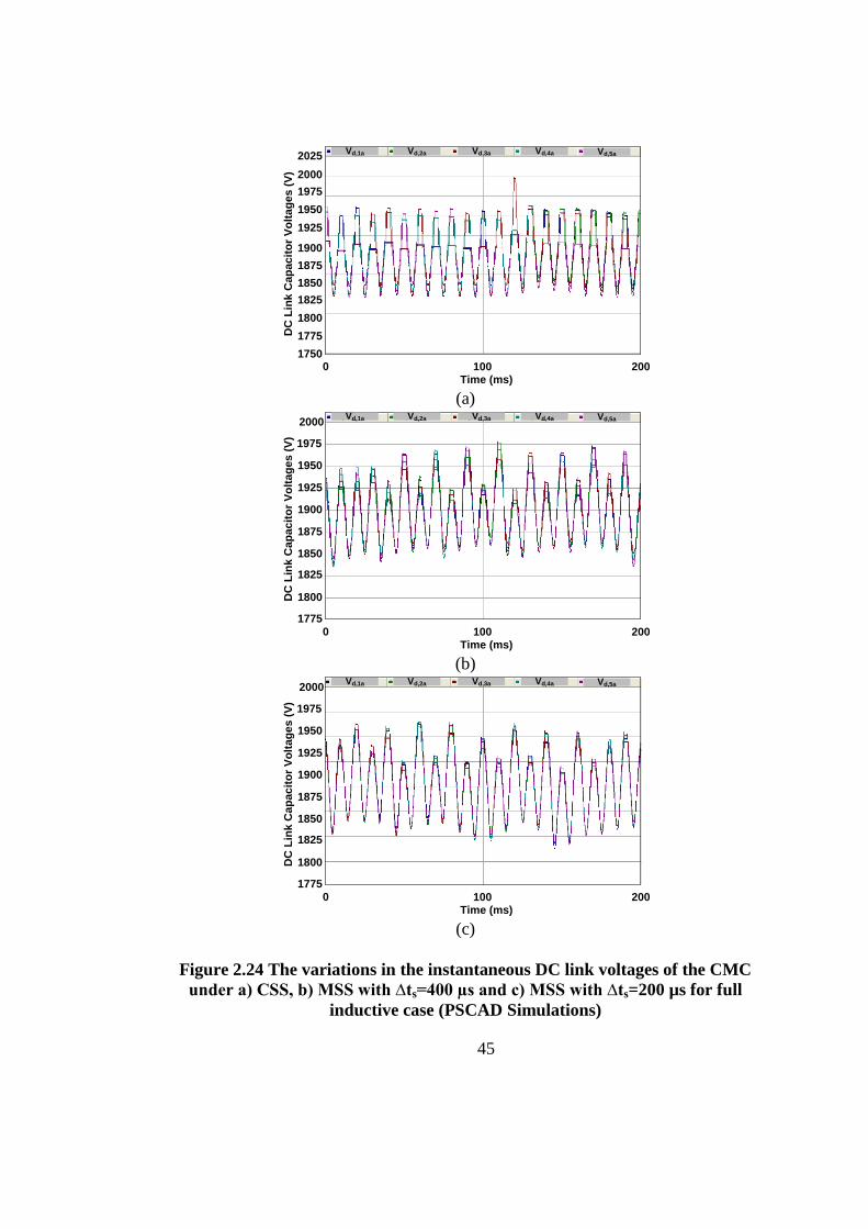
45
(a)
(b)
(c)
Figure 2.24 The variations in the instantaneous DC link voltages of the CMC
under a) CSS, b) MSS with ∆ts=400 µs and c) MSS with ∆ts=200 µs for full
inductive case (PSCAD Simulations)
DC
Lin
k C
ap
ac
ito
r V
olt
ag
es
(V
)
1750
1775
1800
1825
1850
1875
1900
1925
1950
1975
2000
2025
0 100 200Time (ms)
Vd,1a Vd,2a Vd,3a Vd,4a Vd,5a
DC
Lin
k C
ap
ac
ito
r V
olt
ag
es
(V
)
1775
1800
1825
1850
1875
1900
1925
1950
1975
2000
0 100 200
Vd,1a Vd,2a Vd,3a Vd,4a Vd,5a
Time (ms)
DC
Lin
k C
ap
ac
ito
r V
olt
ag
es
(V
)
1775
1800
1825
1850
1875
1900
1925
1950
1975
2000
0 100 200Time (ms)
Vd,1a Vd,2a Vd,3a Vd,4a Vd,5a
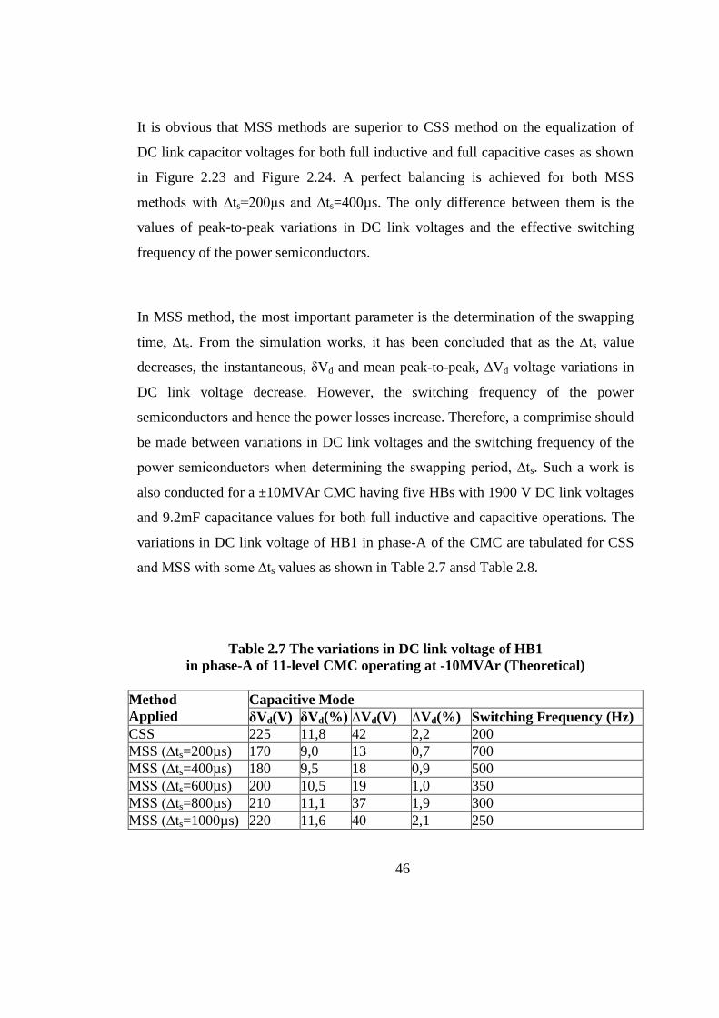
46
It is obvious that MSS methods are superior to CSS method on the equalization of
DC link capacitor voltages for both full inductive and full capacitive cases as shown
in Figure 2.23 and Figure 2.24. A perfect balancing is achieved for both MSS
methods with ∆ts=200µs and ∆ts=400µs. The only difference between them is the
values of peak-to-peak variations in DC link voltages and the effective switching
frequency of the power semiconductors.
In MSS method, the most important parameter is the determination of the swapping
time, ∆ts. From the simulation works, it has been concluded that as the ∆ts value
decreases, the instantaneous, δVd and mean peak-to-peak, ∆Vd voltage variations in
DC link voltage decrease. However, the switching frequency of the power
semiconductors and hence the power losses increase. Therefore, a comprimise should
be made between variations in DC link voltages and the switching frequency of the
power semiconductors when determining the swapping period, ∆ts. Such a work is
also conducted for a ±10MVAr CMC having five HBs with 1900 V DC link voltages
and 9.2mF capacitance values for both full inductive and capacitive operations. The
variations in DC link voltage of HB1 in phase-A of the CMC are tabulated for CSS
and MSS with some ∆ts values as shown in Table 2.7 ansd Table 2.8.
Table 2.7 The variations in DC link voltage of HB1
in phase-A of 11-level CMC operating at -10MVAr (Theoretical)
Method
Applied
Capacitive Mode
δVd(V) δVd(%) ∆Vd(V) ∆Vd(%) Switching Frequency (Hz)
CSS 225 11,8 42 2,2 200
MSS (∆ts=200µs) 170 9,0 13 0,7 700
MSS (∆ts=400µs) 180 9,5 18 0,9 500
MSS (∆ts=600µs) 200 10,5 19 1,0 350
MSS (∆ts=800µs) 210 11,1 37 1,9 300
MSS (∆ts=1000µs) 220 11,6 40 2,1 250

47
Table 2.8 The variations in DC link voltage of HB1
in phase-A of 11-level CMC operating at +10MVAr (Theoretical)
Method
Applied
Inductive Mode
δVd(V) δVd(%) ∆Vd(V) ∆Vd(%) Switching Frequency (Hz)
CSS 180 9,5 35 1,8 250
MSS (∆ts=200µs) 122 6,4 10 0,5 650
MSS (∆ts=400µs) 120 6,3 10 0,5 500
MSS (∆ts=600µs) 125 6,6 14 0,7 400
MSS (∆ts=800µs) 130 6,8 17 0,9 350
MSS (∆ts=1000µs) 160 8,4 28 1,5 300
The following conclusions can be drawn from the simulation works conducted for
11-level CMC at ±10MVAr ratings:
a. MSS methods are superior to CSS method on the equalization of DC link
capacitor voltages for both full inductive and full capacitive operation modes.
b. Although the effective switching frequency of the power semiconductors
under CSS method is less, the variations in instantaneous peak-to-peak and
mean voltages of DC link voltages for HBs are higher than those of under
MSS method. This is an important result since it gives a chance to choose a
lower capacitance value for MSS method than CSS method for the same
design value of DC link instantaneous peak-to-peak voltage. As an example,
the instantaneous peak-to-peak DC link voltage of HB1 under CSS method is
180 V while it is 120V when MSS with ∆ts=400µs is employed to the same
HB unit. There is a 33% decrease in variations in DC link voltages of each
HB under MSS method which may result in using the capacitance values of
0.67 times of those for HBs under CSS method. Therefore, it is economically
beneficial to apply MSS method especially for the CMCs having high number
of HBs in series for high voltage- high power applications.

48
c. The variations in instantaneous peak-to-peak and mean voltages decrease
with MSS methods with low values of ∆ts while the effective switching
frequency of power semiconductors increases. Therefore, for practical
applications, a compromise should be made between the instantaneous peak-
to-peak voltage and the effective switching frequency.
d. For full inductive operation mode, all CSS and MSS methods achieve the
percentage limit value for the variations in peak-to-peak DC link voltage for
an HB unit as shown in Figure 2.25.
e. The variations in the DC link instantaneous peak-to-peak voltage of an HB
unit is over the limit value for CSS method applied to the CMC at 10 MVAr
capacitive operation mode as shown in Figure 2.25. Also, MSS method with
∆ts=200µs and ∆ts=400µs can only achieve the design value for both full
capacitive and inductive operation modes.
f. Beyond a ∆ts value such as ∆ts=1000µs, no difference exists between CSS
and MSS methods for variations in DC link instantaneous peak-to-peak
voltages.
Figure 2.25 The performance of CSS and MSS methods on the instantaneous
peak-to-peak variations in the DC link voltage of an HB unit (Theoretical)
Limit Value
(Rule of Thumb)
CSS

49
In the field tests of the T-STATCOM, the MSS has been applied at a pre-specified
period of ∆ts=400µs and also of ∆ts=200µs, at the expense of higher switching
frequency and hence switching losses. The effects of MSS on voltage balancing
problem and switching frequency will be discussed in Chapter 5 of the thesis in
comparison with those of CSS by field test results.

50
CHAPTER 3
SYSTEM DESIGN AND SIZING
3.1 Introduction
This chapter of the thesis describes the general principles applicable to the design of
the T-STATCOM systems in view of:
a. IEEE harmonic standards,
b. supply conditions,
c. ratings of power semiconductors available in the market,
d. reactive power demand of the over-headline or transmission bus to which the
T-STATCOM is connected.
These design issues include:
a. the sizing of H-Bridge (HB) and Cascaded Multilevel Converter (CMC),
b. the determination of the number HBs in each phase of the CMC,
c. the determination of the number of parallel operated CMCs
d. the calculation of optimum value of total series filter reactance.
3.2 Determination of Connection Point and Sizing of T-
STATCOM
A T-STATCOM system may be connected to the power grid in two different ways as
summarized in Figure 3.1 and Figure 3.2. The existing parts of the power grid are
shown by grey-colored components in Figure 3.1 and Figure 3.2., while the major

51
components of the T-STATCOM by black-colored lines. If a power transformer
operating at partial loads is present in the area at which the T-STATCOM system
will be installed, the T-STATCOM may be connected to the MV side of this
transformer as shown in Figure 3.1. For this case, the Point of Common Coupling
(PCC) should be taken as the MV side of the power transformer.
(a)
(b)
Figure 3.1 Connection alternatives for T-STATCOM system ((a) and (b)
connection to the MV side of existing power transformer)
Alternatively, the T-STATCOM system may be connected to one of the EHV or HV
buses at the same location of the power grid via a specially designed coupling
transformer as shown in Figure 3.2.
MV(E)HV to
LOADS
PCC
Coupling
Reactor CMC Module
Power
Transformer
Po
we
r
Gri
d
MV(E)HV to
LOADS
PCC
Coupling
Reactor-1 CMC Module-1
Power
Transformer
CMC Module-m
Coupling
Reactor-m
...
Po
we
r
Gri
d
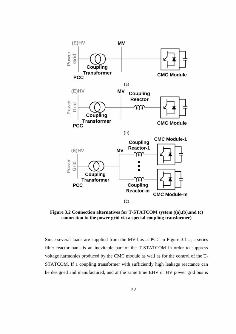
52
(a)
(b)
(c)
Figure 3.2 Connection alternatives for T-STATCOM system ((a),(b),and (c)
connection to the power grid via a special coupling transformer)
Since several loads are supplied from the MV bus at PCC in Figure 3.1-a, a series
filter reactor bank is an inevitable part of the T-STATCOM in order to suppress
voltage harmonics produced by the CMC module as well as for the control of the T-
STATCOM. If a coupling transformer with sufficiently high leakage reactance can
be designed and manufactured, and at the same time EHV or HV power grid bus is
MV(E)HV
PCCCMC Module
Coupling
TransformerP
ow
er
Gri
d
MV(E)HV
PCC
Coupling
Reactor
CMC Module
Coupling
Transformer
Po
we
r
Gri
d
MV(E)HV
PCC
Coupling
Reactor-1
CMC Module-1
Coupling
Transformer
CMC Module-m
Coupling
Reactor-m
...
Po
we
r
Gri
d
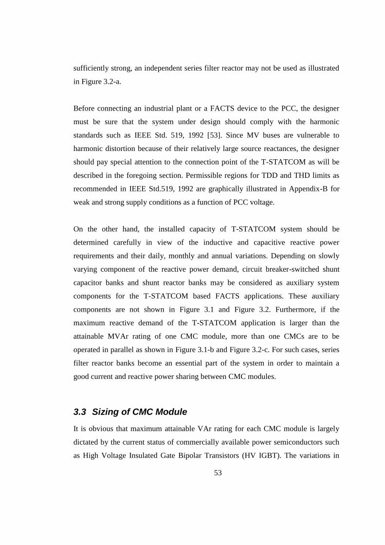
53
sufficiently strong, an independent series filter reactor may not be used as illustrated
in Figure 3.2-a.
Before connecting an industrial plant or a FACTS device to the PCC, the designer
must be sure that the system under design should comply with the harmonic
standards such as IEEE Std. 519, 1992 [53]. Since MV buses are vulnerable to
harmonic distortion because of their relatively large source reactances, the designer
should pay special attention to the connection point of the T-STATCOM as will be
described in the foregoing section. Permissible regions for TDD and THD limits as
recommended in IEEE Std.519, 1992 are graphically illustrated in Appendix-B for
weak and strong supply conditions as a function of PCC voltage.
On the other hand, the installed capacity of T-STATCOM system should be
determined carefully in view of the inductive and capacitive reactive power
requirements and their daily, monthly and annual variations. Depending on slowly
varying component of the reactive power demand, circuit breaker-switched shunt
capacitor banks and shunt reactor banks may be considered as auxiliary system
components for the T-STATCOM based FACTS applications. These auxiliary
components are not shown in Figure 3.1 and Figure 3.2. Furthermore, if the
maximum reactive demand of the T-STATCOM application is larger than the
attainable MVAr rating of one CMC module, more than one CMCs are to be
operated in parallel as shown in Figure 3.1-b and Figure 3.2-c. For such cases, series
filter reactor banks become an essential part of the system in order to maintain a
good current and reactive power sharing between CMC modules.
3.3 Sizing of CMC Module
It is obvious that maximum attainable VAr rating for each CMC module is largely
dictated by the current status of commercially available power semiconductors such
as High Voltage Insulated Gate Bipolar Transistors (HV IGBT). The variations in

54
maximum allowable peak current in commercially available HV IGBTs by June
2012 are given in Appendix-C as a function of the DC link voltage of HB. By using
these data, maximum attainable CMC ratings (± ) are calculated as a function of
rated AC voltage of CMC (Vc) for three different CMC topologies with three, five
and seven series connected HBs and given in Figure 3.3. Rated AC voltage of CMC
in Figure 3.3 can be chosen among the standard AC voltages specified in IEC
Standard Voltages [54]. This voltage is determined by the coupling transformer
secondary voltage to which CMC module is to be connected as described in
Subsection III-A. DC link voltages, Vd of each HB in the CMC are marked on Figure
3.3 for each CMC topology and for all CMC voltages. For these Vd values, rated
collector-emitter voltages and maximum rated collector currents of commercially
available HV IGBTs can be read from the figure given in Appendix-B. Therefore the
maximum attainable CMC ratings in Figure 3.3 are calculated by PSCAD
simulations by considering collector-emitter voltage ratings, maximum available
collector current ratings, Safe Operating Areas (SOAs) of the required HV IGBTs
and the number of HBs in each phase of associated CMC.
It is seen from Figure 3.3 that maximum ratings of each CMC module are
obtained for seven series connected HBs in each phase and utilizing 1700V, 3600A
and 6500V, 750A HV IGBTs respectively for 7.2 kV and 36 kV line-to-line CMC
voltage ratings. Although, this choice (seven HB in series, l=15 levels in line-to-
neutral voltages) yields minimum harmonic distortion in line-to-line voltages and
line currents, its major drawback is the complexity of the power stage and the control
system.
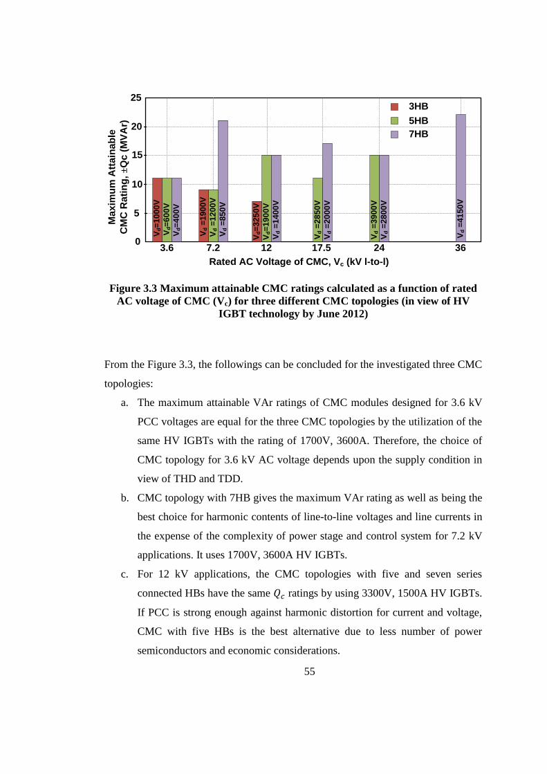
55
Figure 3.3 Maximum attainable CMC ratings calculated as a function of rated
AC voltage of CMC (Vc) for three different CMC topologies (in view of HV
IGBT technology by June 2012)
From the Figure 3.3, the followings can be concluded for the investigated three CMC
topologies:
a. The maximum attainable VAr ratings of CMC modules designed for 3.6 kV
PCC voltages are equal for the three CMC topologies by the utilization of the
same HV IGBTs with the rating of 1700V, 3600A. Therefore, the choice of
CMC topology for 3.6 kV AC voltage depends upon the supply condition in
view of THD and TDD.
b. CMC topology with 7HB gives the maximum VAr rating as well as being the
best choice for harmonic contents of line-to-line voltages and line currents in
the expense of the complexity of power stage and control system for 7.2 kV
applications. It uses 1700V, 3600A HV IGBTs.
c. For 12 kV applications, the CMC topologies with five and seven series
connected HBs have the same ratings by using 3300V, 1500A HV IGBTs.
If PCC is strong enough against harmonic distortion for current and voltage,
CMC with five HBs is the best alternative due to less number of power
semiconductors and economic considerations.
3.6
Rated AC Voltage of CMC, Vc (kV l-to-l)
Ma
xim
um
Att
ain
ab
le
CM
C R
ati
ng
, ±Q
c (
MV
Ar)
7.2
Vd=
10
00V
10
15
20
25
Vd=
40
0V
Vd=
60
0V
Vd =
85
0V
Vd =
19
00V
Vd =
12
00V
12
Vd =
14
00
V
Vd=
32
50
V
Vd=
19
00
V
17.5
Vd =
20
00
V
Vd =
28
50
V
24
Vd =
28
00
V
Vd =
39
00
V
36
Vd =
41
50V
5
0
3HB
5HB
7HB
56
d. CMC topologies with five and seven HBs are only the applicable alternatives
for 17.5kV and 24 kV AC rated voltages. The maximum rating is obtained
by CMC topology with seven HBs by the use of 4500V, 1200A HV IGBTs
for 17.5 kV applications. 6500V, 900A HV IGBTs are utilized in the power
stages of the CMC topologies with five and seven HBs for 24kV. Since both
topologies have the same MVAr capacity, TDD and THD considerations of
the power system at which T-STATCOM is connected determine the choice
among them.
e. The CMC with seven HBs is the only applicable solution for 36 kV
STATCOM applications by using 6500V, 900A HV IGBT modules.
The CMC topology with five series connected HBs is a compromise between system
complexity and maximization of the CMC VAr rating. In this work, a field prototype
of 12kV line-to-line, 11-level CMC is designed and implemented by using 3300V,
1200A HV IGBTs (MITSUBISHI CM1200HC-66H). This CMC can produce
successfully ±12MVAr at its terminals and the resulting T-STATCOM can deliver
10 MVAr capacitive to and absrob 14 MVAr inductive from 154kV PCC. These
practical values verify the findings for 12 kV line-to-line rated AC voltage of 11-
level CMC in Figure 3.3 (rated would be ±15 MVAr if 3300V, 1500A HV IGBT
were used).
3.4 Design of Series Filter Reactor
The performance of the T-STATCOM system at PCC in view of voltage and current
harmonic distortion limits specified in [53] is affected not only by the short-circuit
MVA of busbar to which the T-STATCOM is connected and the number of HBs in
each phase of the CMC but also by the inductance of the total series filter reactor.
Therefore, the choice of the series Lr is a critical issue in the system design. For the
whole results obtained in this subsection, it is assumed that PCC voltage is 12 kV

57
line-to-line, T-STATCOM rating is ±10MVAr and before the connection of the T-
STATCOM, voltage waveforms at PCC are purely sinusoidal.
3.4.1 THD Values in AC Input Voltage of CMC
The THD values in AC input voltage of CMC topologies with three, five and seven
HBs are given in Figure 3.4 for full inductive and full capacitive operating modes.
For capacitive operation mode, the THD values decreases as series filter inductance
value increases. However, only CMC topology with seven HBs is under the limit
value specified by IEEE 519-1992. The THD values of all three topologies
investigated in this work for full inductive operation mode increase and are over the
limit value as the series inductance value increases. This is due to lower modulation
index values corresponding to higher inductive reactive power consumed by large
inductances. As the modulation index values are getting smaller during inductive
mode of operation, the widths of the HBs output voltages are being narrowed, and
hence the AC input voltages of the CMC have more harmonic content. Therefore, the
THD value in AC input voltage of CMC rises when the series filter inductance takes
higher values. For capacitive case, when series filter inductance value rises, to
compansate the voltage drop on it, a higher modulation index value is used and the
widths of output voltages of HBs are being expanded. Therefore, the AC input
voltages of the CMC have less harmonic content than those for inductive operation
mode.
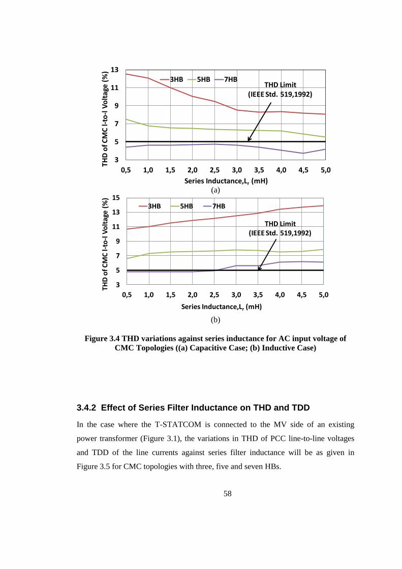
58
(a)
(b)
Figure 3.4 THD variations against series inductance for AC input voltage of
CMC Topologies ((a) Capacitive Case; (b) Inductive Case)
3.4.2 Effect of Series Filter Inductance on THD and TDD
In the case where the T-STATCOM is connected to the MV side of an existing
power transformer (Figure 3.1), the variations in THD of PCC line-to-line voltages
and TDD of the line currents against series filter inductance will be as given in
Figure 3.5 for CMC topologies with three, five and seven HBs.
3
5
7
9
11
13
0,5 1,0 1,5 2,0 2,5 3,0 3,5 4,0 4,5 5,0
THD
of C
MC
l-to
-l V
olt
age
(%
)
Series Inductance,Lr (mH)
3HB 5HB 7HBTHD Limit
(IEEE Std. 519,1992)
3
5
7
9
11
13
15
0,5 1,0 1,5 2,0 2,5 3,0 3,5 4,0 4,5 5,0
THD
of C
MC
l-to
-l V
olt
age
(%)
Series Inductance,Lr (mH)
3HB 5HB 7HB
THD Limit (IEEE Std. 519,1992)
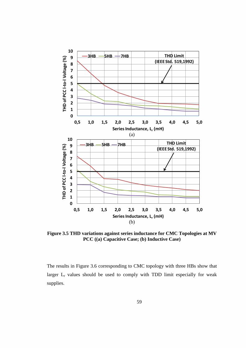
59
(a)
(b)
Figure 3.5 THD variations against series inductance for CMC Topologies at MV
PCC ((a) Capacitive Case; (b) Inductive Case)
The results in Figure 3.6 corresponding to CMC topology with three HBs show that
larger Lr values should be used to comply with TDD limit especially for weak
supplies.
0
1
2
3
4
5
6
7
8
9
10
0,5 1,0 1,5 2,0 2,5 3,0 3,5 4,0 4,5 5,0
THD
of P
CC
l-to
-l V
olt
age
(%
)
Series Inductance, Lr (mH)
3HB 5HB 7HB THD Limit (IEEE Std. 519,1992)
0
1
2
3
4
5
6
7
8
9
10
0,5 1,0 1,5 2,0 2,5 3,0 3,5 4,0 4,5 5,0
THD
of P
CC
l-to
-l V
olt
age
(%)
Series Inductance, Lr (mH)
3HB 5HB 7HB THD Limit (IEEE Std. 519,1992)
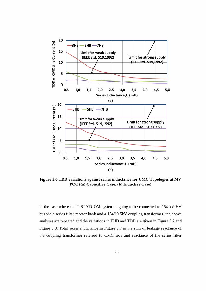
60
(a)
(b)
Figure 3.6 TDD variations against series inductance for CMC Topologies at MV
PCC ((a) Capacitive Case; (b) Inductive Case)
In the case where the T-STATCOM system is going to be connected to 154 kV HV
bus via a series filter reactor bank and a 154/10.5kV coupling transformer, the above
analyses are repeated and the variations in THD and TDD are given in Figure 3.7 and
Figure 3.8. Total series inductance in Figure 3.7 is the sum of leakage reactance of
the coupling transformer referred to CMC side and reactance of the series filter
0
5
10
15
20
0,5 1,0 1,5 2,0 2,5 3,0 3,5 4,0 4,5 5,0
TDD
of C
MC
Lin
e C
urr
en
t (%
)
Series Inductance,Lr (mH)
3HB 5HB 7HB
Limit for weak supply(IEEE Std. 519,1992) Limit for strong supply
(IEEE Std. 519,1992)
0
5
10
15
20
0,5 1,0 1,5 2,0 2,5 3,0 3,5 4,0 4,5 5,0
TD
D o
f C
MC
Lin
e C
urr
en
t (%
)
Series Inductance,Lr (mH)
3HB 5HB 7HB
Limit for strong supply(IEEE Std. 519,1992)
Limit for weak supply(IEEE Std. 519,1992)
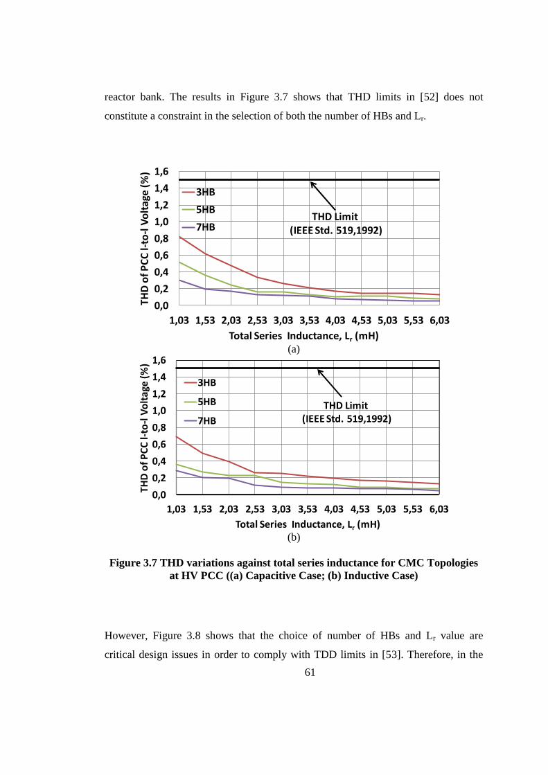
61
reactor bank. The results in Figure 3.7 shows that THD limits in [52] does not
constitute a constraint in the selection of both the number of HBs and Lr.
(a)
(b)
Figure 3.7 THD variations against total series inductance for CMC Topologies
at HV PCC ((a) Capacitive Case; (b) Inductive Case)
However, Figure 3.8 shows that the choice of number of HBs and Lr value are
critical design issues in order to comply with TDD limits in [53]. Therefore, in the
0,0
0,2
0,4
0,6
0,8
1,0
1,2
1,4
1,6
1,03 1,53 2,03 2,53 3,03 3,53 4,03 4,53 5,03 5,53 6,03
THD
of P
CC
l-to
-l V
olt
age
(%
)
Total Series Inductance, Lr (mH)
3HB
5HB
7HBTHD Limit
(IEEE Std. 519,1992)
0,0
0,2
0,4
0,6
0,8
1,0
1,2
1,4
1,6
1,03 1,53 2,03 2,53 3,03 3,53 4,03 4,53 5,03 5,53 6,03
THD
of P
CC
l-to
-l V
olt
age
(%
)
Total Series Inductance, Lr (mH)
3HB
5HB
7HB
THD Limit (IEEE Std. 519,1992)

62
design of the field prototype of the T-STATCOM system, a CMC with five HBs
should be preferred and a total series inductance greater than 2.75mH should be
chosen.
(a)
(b)
Figure 3.8 TDD variations against total series inductance for CMC Topologies
at HV PCC ((a) Capacitive Case; (b) Inductive Case)
0
2
4
6
8
10
12
14
16
18
20
1,03 1,53 2,03 2,53 3,03 3,53 4,03 4,53 5,03 5,53 6,03
TDD
of
CM
C L
ine
Cu
rre
nt
(%)
Total Series Inductance,Lr ( mH)
3HB 5HB 7HB
Limit for strong supply(IEEE Std. 519,1992)
Limit for weak supply(IEEE Std. 519,1992)
0
2
4
6
8
10
12
14
16
1,03 1,53 2,03 2,53 3,03 3,53 4,03 4,53 5,03 5,53 6,03
TDD
of C
MC
Lin
e C
urr
ent (
%)
Total Series Inductance,Lr (mH)
3HB 5HB 7HB
Limit for strong supply(IEEE Std. 519,1992)
Limit for weak supply(IEEE Std. 519,1992)
63
3.4.3 Effect of Series Filter Inductance on DC Link Voltage and
Modulation Index Values
Another factor affecting the choice of total series inductance, Lr is the design value
of DC link voltage. It is highly desirable to keep DC link voltage constant at the
design value from full inductive to full capacitive operation modes for an ideal T-
STATCOM system. The variations in DC link voltage, Vd, against total series
inductance, Lr, for different values of modulation index, M for the investigated CMC
topologies with three,five and seven HBs are shown in Figure 3.9 - Figure 3.11. The
optimum values of Lr and the associated M ranges are marked on the same figures. Lr
values for CMC topologies are chosen according to THD and TDD values explained
in Subsection 3.4.2.
The CMC with three HBs can achieve the TDD limit value only for Lr value greater
than 4.3mH as seen in Figure 3.8 when the CMC is installed at a strong supply for
full inductive operation mode. For weak supply conditions, this topology can comply
with harmonic standards specified in IEEE 519-1992 for very large Lr values which
may not be feasible. The maximum safe value of DC link voltage for the chosen HV
IGBTs was 3250V as seen in Figure 3.3. The optimum operation point for the CMC
with three HBs is marked on Figure 3.9 with the the choices of Lr=4.3mH and
Vd=3250 V. Therefore, the corresponding M range is [1.66-2.32] as shown in Figure
3.9.
The minimum Lr value to overcome THD and TDD limit values specified by IEEE
519-1992 for CMC having seven HBs is 1.4mH as shown in Figure 3.8. The
maximum safe value of DC link voltage for the chosen HV IGBTs was chosen
1400V as can be seen in Figure 3.3. A total series inductance value greater than
1.4mH should be applied to the CMC design to have a higher resolution in reactive
power variation against load changes. Therefore, Lr=2.53mH is chosen, and the M
value will vary between 4.16 and 4.93 as can be seen in Figure 3.10.

64
Figure 3.9 Variations in DC link voltage against total series inductance for
different values of modulation index, M in the case of CMC with
3HBs/Theoretical
Figure 3.10 Variations in DC link voltage against total series inductance for
different values of modulation index, M in the case of CMC with
7HBs/Theoretical
2500
3000
3500
4000
4500
5000
5500
1,03 1,53 2,03 2,53 3,03 3,53 4,03 4,53 5,03 5,53 6,03
DC
Lin
k V
olt
age
, Vd
(Vo
lts)
Total Series Inductance, Lr (mH)3HB Case
M=2.16
M=2.06
M=1.96
M=1.86
M=1.76
M=1.66
M=2.52
M=2.42M=2.32
M=2.22M=2.12
M=2.02 Capacitive
Inductive
Lr=4.4mH
Chosen M Range
1.66 ≤ M ≤2.32
M=3.96M=3.86
1100
1200
1300
1400
1500
1600
1700
1800
1900
1,03 1,53 2,03 2,53 3,03 3,53 4,03 4,53 5,03 5,53 6,03
DC
Lin
k V
olt
age
,Vd
(V)
Total Series Inductance, Lr (mH)7HB Case
M=5.73M=5.63M=5.53M=5.43M=5.33M=5.23M=5.13
M=5.03M=4.93
M=4.06
M=3.76
M=3.66M=3.56M=3.46
M=3.36
M=3.26
M=3.96M=3.86
Lr = 2.53mH
Chosen M Range
4.16 ≤ M ≤ 4.93
Capacitive
Inductive
M=4.93
M=4.16

65
For CMC topology with five HBs, as can be understood from this Figure 3.11, M can
be varied between 2.5 and 4.23 for the chosen CMC topology with SHEM. Although
such a wide variation range for M improves the resolution in VAr generation, this
choice needs a very large Lr resulting in very high CMC voltage regulation and
reactor losses. The minimum permissible value of Lr for the field prototype was
found to be 2.75mH (Figure 3.8) and maximum safe value of the mean DC link
voltage for the chosen HV IGBTs was 1900V (Figure 3.3). If Lr=2.75mH were
chosen in the design, M will vary in between 3.63 and 3.10 from full capacitive to
full inductive operation mode as shown in Figure 3.11. This is obviously a narrow
variation range for M.
Figure 3.11 Variations in DC link voltage against total series inductance for
different values of modulation index, M in the case of CMC with
5HBs/Theoretical
Therefore, in the design and implementation of the field prototype of the T-
STATCOM, a total series inductance of Lr = 3.53 mH (1.03 mH transformer leakage
1500
1600
1700
1800
1900
2000
2100
2200
2300
2400
2500
1,03 1,53 2,03 2,53 3,03 3,53 4,03 4,53 5,03 5,53 6,03
Ax
is T
itle
Axis TitleTotal Series Inductance, Lr (mH)
1.03 1.53 2.03 2.53 3.03 3.53 4.03 4.53 5.03 5.53 6.03
1500
1600
1700
1800
1900
2000
2100
2200
2300
2400
2500
DC
Lin
k V
olt
ag
e, V
d (
V)
M=2.5
M=2.6
M=2.7
M=2.8
M=2.9
M=3.0
M=3.1
M=4.23M=4.13M=4.03
M=3.93M=3.83M=3.73
M=3.63
Lr =3.53mH chosen
Chosen M range
3.0 ≤ M ≤ 3.73
Inductive
Capacitive
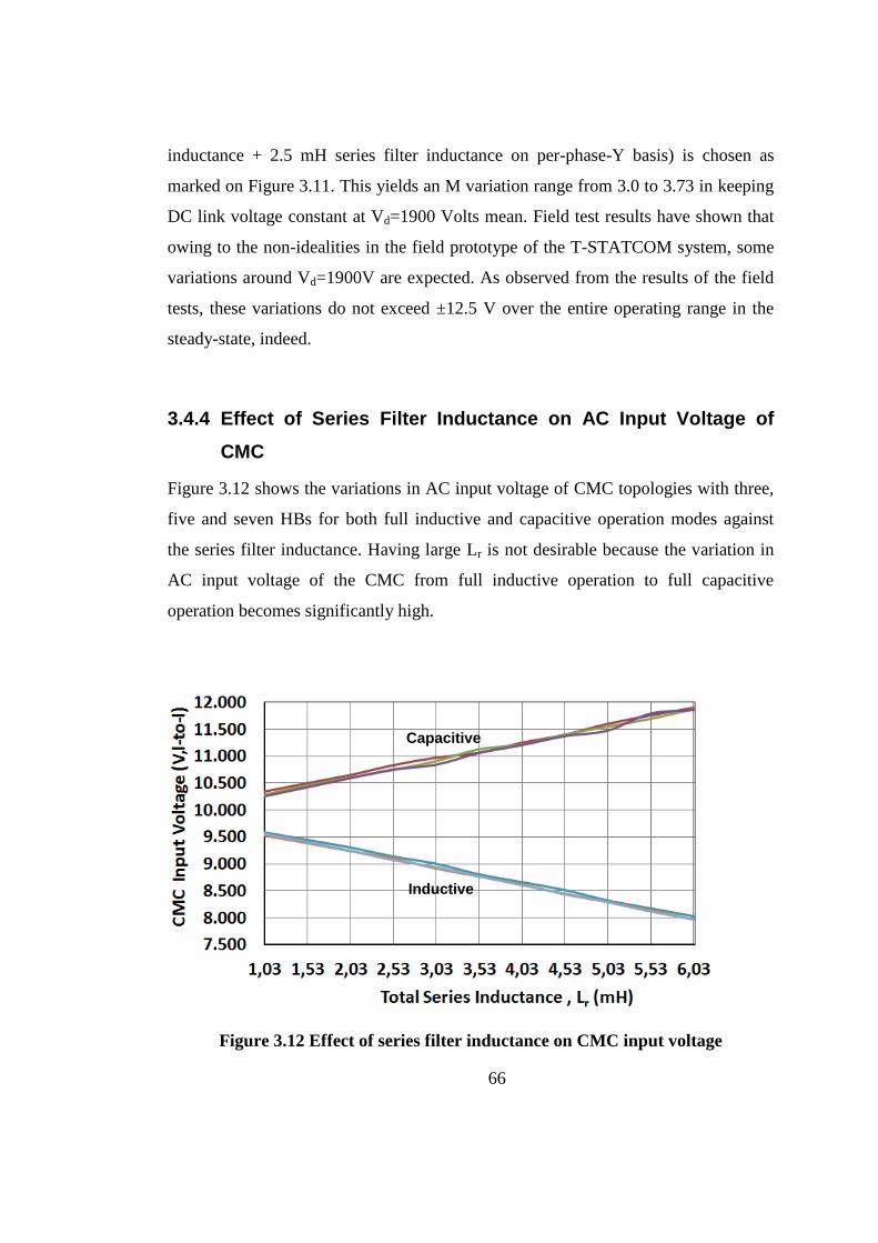
66
inductance + 2.5 mH series filter inductance on per-phase-Y basis) is chosen as
marked on Figure 3.11. This yields an M variation range from 3.0 to 3.73 in keeping
DC link voltage constant at Vd=1900 Volts mean. Field test results have shown that
owing to the non-idealities in the field prototype of the T-STATCOM system, some
variations around Vd=1900V are expected. As observed from the results of the field
tests, these variations do not exceed ±12.5 V over the entire operating range in the
steady-state, indeed.
3.4.4 Effect of Series Filter Inductance on AC Input Voltage of
CMC
Figure 3.12 shows the variations in AC input voltage of CMC topologies with three,
five and seven HBs for both full inductive and capacitive operation modes against
the series filter inductance. Having large Lr is not desirable because the variation in
AC input voltage of the CMC from full inductive operation to full capacitive
operation becomes significantly high.
Figure 3.12 Effect of series filter inductance on CMC input voltage
Capacitive
Inductive
67
Therefore, in order to keep voltage regulation of the CMC at a reasonable low value,
a series filter reactor bank with relatively small Lr should be chosen.
3.4.5 Conclusions
The followings can be concluded from the work carried out in this chapter:
a. When connecting a T-STATCOM system to an existing power transformer, a
series filter reactor bank/s should be used for both the use of a single and
paralleled CMCs.
b. When specially designed transformer is only used for a T-STATCOM
system, the series filter reactor bank may not be used for a single CMC
module if leakage reactance of the transformer is sufficient. When CMC
modules are used in parallel to reach higher MVAr ratings for T-STATCOM
systems, it is compulsory to use series filter reactor banks to share current
equally and for control purposes.
c. The maximum attainable VAr rating for CMC modules is largely dictated by
the current status of commercially available power semiconductors such as
High Voltage Insulated Gate Bipolar Transistors (HV IGBTs).
d. The number of HBs in series for CMC topology is not only the parameter on
complying with THD and TDD limits specified in IEEE 519-1992. The series
filter inductance value has also a great effect on THD and TDD limits.
Therefore, chosing Lr value for CMC topologies is a crucial issue when
designing the system.
e. As the value of series filter inductance rises, the THD and TDD values
decrease for CMC topologies with three, five and seven HBs while the
variations in AC input voltage of the CMC from full inductive operation to
full capacitive operation becomes significantly high.
f. There is an optimum point of DC link voltages and M-range values for each
CMC topology in view of complying with THD and TDD limits.
g. The effects of series filter inductance value on the system design are shown in
Table 3.1.
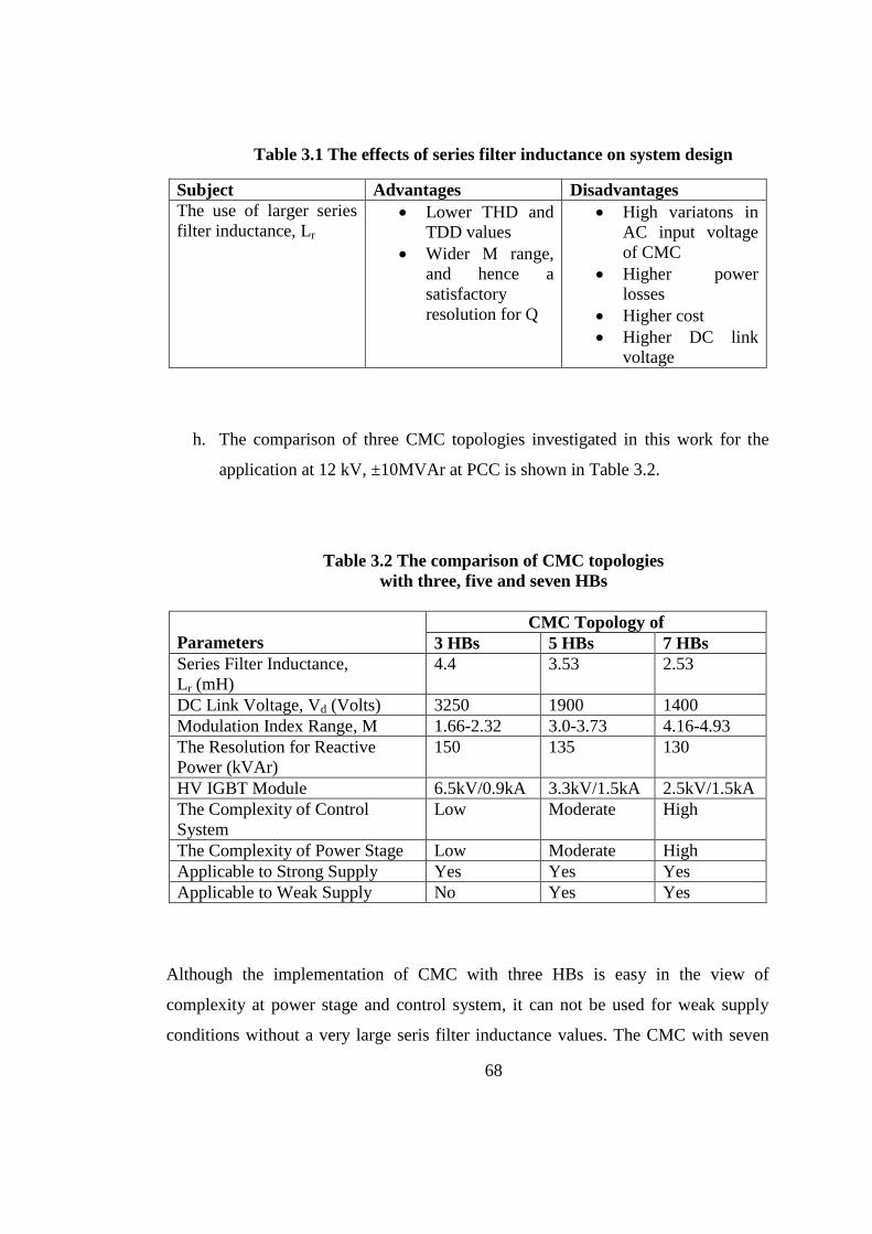
68
Table 3.1 The effects of series filter inductance on system design
Subject Advantages Disadvantages
The use of larger series
filter inductance, Lr Lower THD and
TDD values
Wider M range,
and hence a
satisfactory
resolution for Q
High variatons in
AC input voltage
of CMC
Higher power
losses
Higher cost
Higher DC link
voltage
h. The comparison of three CMC topologies investigated in this work for the
application at 12 kV, ±10MVAr at PCC is shown in Table 3.2.
Table 3.2 The comparison of CMC topologies
with three, five and seven HBs
Parameters
CMC Topology of
3 HBs 5 HBs 7 HBs
Series Filter Inductance,
Lr (mH)
4.4 3.53 2.53
DC Link Voltage, Vd (Volts) 3250 1900 1400
Modulation Index Range, M 1.66-2.32 3.0-3.73 4.16-4.93
The Resolution for Reactive
Power (kVAr)
150 135 130
HV IGBT Module 6.5kV/0.9kA 3.3kV/1.5kA 2.5kV/1.5kA
The Complexity of Control
System
Low Moderate High
The Complexity of Power Stage Low Moderate High
Applicable to Strong Supply Yes Yes Yes
Applicable to Weak Supply No Yes Yes
Although the implementation of CMC with three HBs is easy in the view of
complexity at power stage and control system, it can not be used for weak supply
conditions without a very large seris filter inductance values. The CMC with seven

69
HBs in the best solution for yielding minimum harmonic distortion in line-to-line
voltages and line currents, its major drawback is the complexity of the power stage
and the control system. Therefore, the CMC topology with five series connected HBs
is a compromise between system complexity and maximization of the CMC VAr
rating. In this work, a field prototype of 12kV line-to-line, ±10MVAr, 11-level CMC
module is designed and implemented by using 3300V, 1200A HV IGBTs.

70
CHAPTER 4
DESIGN OF A CASCADED MULTILEVEL
CONVERTER (CMC) MODULE
4.1 Design of CMC Module
In this work, a 3-phase, Y-connected, 11-level (n=5), ±12MVAr H-Bridge based
Cascaded Multilevel Converter (CMC) module shown in Figure 4.1 is designed and
implemented. AC voltage of the CMC is chosen to be Vc = 12 kV line-to- line and its
constant DC link voltage is Vdc=9500V. In each phase of the CMC, five HB circuits
are connected in series and the DC link voltage of the designed HB is Vd=1900Volts
mean. HB units used in each phase of CMC module have been placed on the shelves
which are built up of a specially designed Glass-fiber Reinforced Polyester (GRP)
with 3x5 matrix structure as shown in Figure 4.1.
In this section, the design considerations for CMC module and the HB circuit with
the selection of its major components like power semiconductors, laminated busbars,
and DC link capacitors have been presented. Moreover, the control system with its
structure and its major functions for a CMC module is also given in this section. The
designed and implemented 12kV, ±12MVAR, 11-level CMC module is the basic

71
building block for large T-STATCOM systems. It is possible to reach larger MVAr
ratings of T-STATCOM systems by parallel use of these CMC modules.
Figure 4.1 Designed and implemented 3-phase, 12kV, ±12 MVAr, Y-connected
11-level CMC module
4.1.1 Design of the H-Bridge (HB) Circuit
H-Bridge circuits are the basic units for the power stages of CMC modules. In fact, n
number of HBs can be connected in series for each phase of CMC to reach the

72
desired AC voltage at which CMC is implemented. This gives a modularized circuit
layout and packaging for CMC due to the usage of the same structure for each level.
4.1.1.1 The structure and operation of HB Circuits
Figure 4.2 shows the single line diagram of an H-Bridge (HB) circuit with its typical
output voltage. In an HB circuit, as power semiconductors, there are four
conventional wire-bond HV IGBT modules in which antiparallel diodes are used
with IGBT parts in the same packages. These IGBT modules are mounted on cold
plates for high power practical applications. The DC link capacitors are connected to
these IGBT modules via (+) and (-) DC buses which are designed generally as
laminated busbars. Gate Drive (GD) circuits are used to control each IGBT module
as shown in Figure 4.2.
The output voltage of an HB circuit have three voltage levels of the, namely +Vd, 0
and –Vd. The polarity of the output voltage of the HB is positive, and equal to the DC
link voltage, +Vd if HV IGBT modules of 1 and 3 are triggerred to conduction while
the polarity of output voltage is negative, and equal to –Vd if HV IGBT modules of 2
and 4 are triggerred to conduction as shown in Figure 4.2-b. The operation states of
the IGBT and diode parts of the HV IGBT modules are dependent upon the direction
of the current. As an example, if polarity of the current flowing through the HB
circuit is taken as positive, +Vd is obtained as ouput voltage of HB by the operation
of diodes, D1-D3. The same output voltage is also seen by the operation of S1-S3
when current flowing out of the HB. Zero voltage level exits when current is by-
passed through the DC link voltages. There are four different current paths formed
by the operation of one of the IGBT and diode parts of upper or lower HV IGBT
modules to reach zero voltage level as marked on Figure 4.2-b. The operation states
of the HB circuit is shown in Table 4.1. The direction of the current is taken as
positive when flowing through the HB circuit for the operation states in Table 4.1.
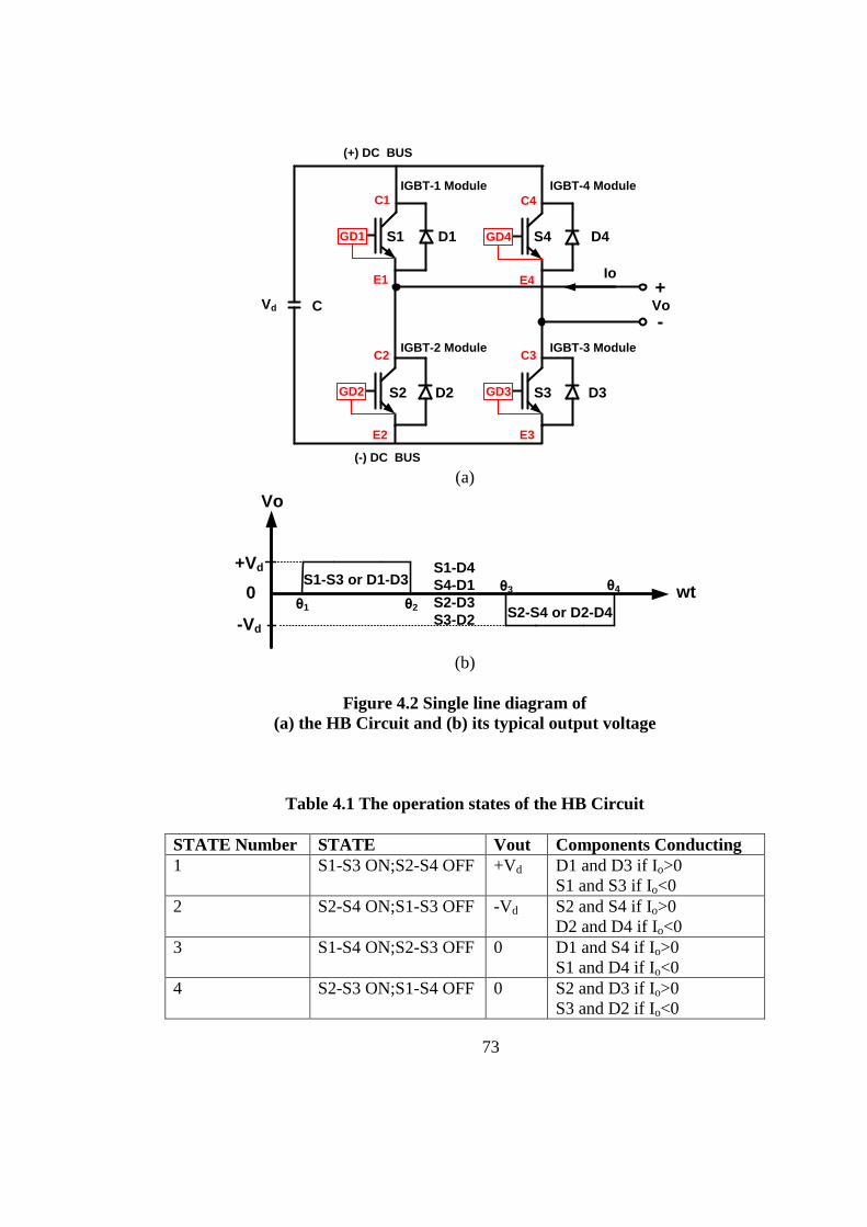
73
(a)
(b)
Figure 4.2 Single line diagram of
(a) the HB Circuit and (b) its typical output voltage
Table 4.1 The operation states of the HB Circuit
STATE Number STATE Vout Components Conducting
1 S1-S3 ON;S2-S4 OFF +Vd D1 and D3 if Io>0
S1 and S3 if Io<0
2 S2-S4 ON;S1-S3 OFF -Vd S2 and S4 if Io>0
D2 and D4 if Io<0
3 S1-S4 ON;S2-S3 OFF 0 D1 and S4 if Io>0
S1 and D4 if Io<0
4 S2-S3 ON;S1-S4 OFF 0 S2 and D3 if Io>0
S3 and D2 if Io<0
Io
(+) DC BUS
+
-VoVd
(-) DC BUS
S1
C1
E1
GD1
C2
E2
GD2
C4
E4
GD4
C3
E3
GD3
C
D1
S2 D2 S3
S4
D3
D4
IGBT-1 Module IGBT-4 Module
IGBT-2 Module IGBT-3 Module
wt
Vo
-Vd
0
+Vd
θ1 θ2
θ3 θ4S1-S3 or D1-D3
S2-S4 or D2-D4
S1-D4
S4-D1
S2-D3
S3-D2

74
(a)
(b)
(c)
(d)
(e)
(f)
(g)
(h)
Figure 4.3 The operation modes of HB: a) Charging-1(CH1), b) Charging-
2(CH2) ,c) Discharging-1 (DCH1), d) Discharging-2 (DCH2), e) By-pass-1
(BYP1), f) By-pass-2 (BYP2), g) By-pass-3 (BYP3), h) By-pass-4 (BYP4)
CH1
+Vc
Io+
Vd
IGBT-1
IGBT-2
IGBT-4
IGBT-3
C
+
-
Io+
IGBT-1
IGBT-2
IGBT-4
IGBT-3
C Vd Vc
CH2
+
-
Io
+
IGBT-1
IGBT-2
IGBT-4
IGBT-3
C VdVc
DCH1
Io+
IGBT-1
IGBT-2
IGBT-4
IGBT-3
C+
-Vd
Vc
DCH2
0
Io+
IGBT-1
IGBT-2
IGBT-4
IGBT-3
C Vd
BYP1 BYP2
0
Io
IGBT-1
IGBT-2
IGBT-4
IGBT-3
+C Vd
0
Io+
IGBT-1
IGBT-2
IGBT-4
C Vd
BYP3
0
Io
IGBT-1
IGBT-2
IGBT-4
IGBT-3
Vd
BYP4
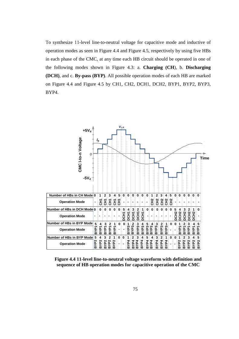
75
To synthesize 11-level line-to-neutral voltage for capacitive mode and inductive of
operation modes as seen in Figure 4.4 and Figure 4.5, respectively by using five HBs
in each phase of the CMC, at any time each HB circuit should be operated in one of
the following modes shown in Figure 4.3: a. Charging (CH), b. Discharging
(DCH), and c. By-pass (BYP). All possible operation modes of each HB are marked
on Figure 4.4 and Figure 4.5 by CH1, CH2, DCH1, DCH2, BYP1, BYP2, BYP3,
BYP4.
Figure 4.4 11-level line-to-neutral voltage waveform with definition and
sequence of HB operation modes for capacitive operation of the CMC
ia
vcA
+5Vd
-5Vd
Number of HBs in CH Mode 0
0
5
1
0
4
2
0
3
3
0
2
4
0
1
5
0
0
0
5
0
0
4
1
5 4 3 2 1 0 0 1
0
3
2
2
0
2
3
3
0
1
4
4
0
0
5
5
1
0
4
4
2
0
3
3
3
0
2
2
4
0
1
1
5
0
0
0
0
5
0
0
0
4
1
1
0
3
2
2
0
2
3
3
0
1
4
4
0
0
5
5
0
Operation Mode -
CH
1
CH
1
CH
1
CH
1
CH
1
- - - - - -
CH
2
CH
2
CH
2
CH
2
CH
2
- - - - - -
- - - - - -
DC
H1
DC
H1
DC
H1
DC
H1
DC
H1
- - - - - -
DC
H2
DC
H2
DC
H2
DC
H2
DC
H2
-
BY
P1
BY
P1
BY
P1
BY
P1
BY
P1
- -
BY
P3
BY
P3
BY
P3
BY
P3
BY
P3
BY
P3
BY
P3
BY
P3
BY
P3
- -
BY
P1
BY
P1
BY
P1
BY
P1
BY
P1
BY
P2
BY
P2
BY
P2
BY
P2
BY
P2
- -
BY
P4
BY
P4
BY
P4
BY
P4
BY
P4
BY
P4
BY
P4
BY
P4
BY
P4
- -
BY
P2
BY
P2
BY
P2
BY
P2
BY
P2
Number of HBs in DCH Mode
Operation Mode
Number of HBs in BYP Mode
Operation Mode
Number of HBs in BYP Mode
Operation Mode
CM
C l-t
o-n
Vo
lta
ge
Time
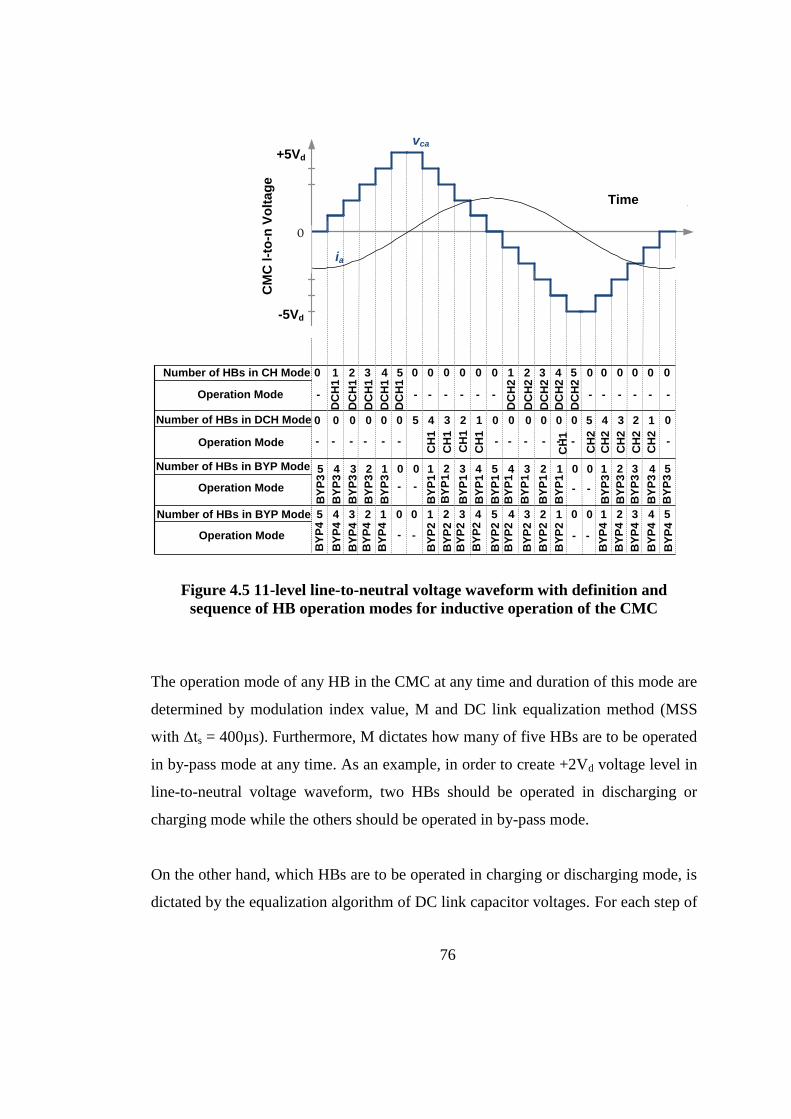
76
Figure 4.5 11-level line-to-neutral voltage waveform with definition and
sequence of HB operation modes for inductive operation of the CMC
The operation mode of any HB in the CMC at any time and duration of this mode are
determined by modulation index value, M and DC link equalization method (MSS
with ∆ts = 400µs). Furthermore, M dictates how many of five HBs are to be operated
in by-pass mode at any time. As an example, in order to create +2Vd voltage level in
line-to-neutral voltage waveform, two HBs should be operated in discharging or
charging mode while the others should be operated in by-pass mode.
On the other hand, which HBs are to be operated in charging or discharging mode, is
dictated by the equalization algorithm of DC link capacitor voltages. For each step of
ia
vca
+5Vd
-5Vd
Number of HBs in CH Mode 0
0
5
1
0
4
2
0
3
3
0
2
4
0
1
5
0
0
0
5
0
0
4
1
5 4 3 2 1 0 0 1
0
3
2
2
0
2
3
3
0
1
4
4
0
0
5
5
1
0
4
4
2
0
3
3
3
0
2
2
4
0
1
1
5
0
0
0
0
5
0
0
0
4
1
1
0
3
2
2
0
2
3
3
0
1
4
4
0
0
5
5
Operation Mode -
CH
1
DC
H1
DC
H1
DC
H1
DC
H1
- - - - - -
DC
H2
DC
H2
DC
H2
DC
H2
DC
H2
- - - - - -
- - - - - -
DC
H1
CH
1
CH
1
CH
1
CH
1
- - - - - -
CH
2
CH
2
CH
2
CH
2
CH
2
-
BY
P3
BY
P3
BY
P3
BY
P3
BY
P3
- -
BY
P1
BY
P1
BY
P1
BY
P1
BY
P1
BY
P1
BY
P1
BY
P1
BY
P1
- -
BY
P3
BY
P3
BY
P3
BY
P3
BY
P3
BY
P4
BY
P4
BY
P4
BY
P4
BY
P4
- -
BY
P2
BY
P2
BY
P2
BY
P2
BY
P2
BY
P2
BY
P2
BY
P2
BY
P2
- -
BY
P4
BY
P4
BY
P4
BY
P4
BY
P4
Number of HBs in DCH Mode
Operation Mode
Number of HBs in BYP Mode
Operation Mode
Number of HBs in BYP Mode
Operation Mode
Time
ia
CM
C l-t
o-n
Vo
lta
ge
0

77
the 11-level line-to-neutral voltage waveform, operation modes for all HBs and the
number of HBs in each mode are also marked in Figure 4.4 and Figure 4.5. In order
to avoid complexity in the explanations, the theoretical line-to-neutral voltage
waveform and associated table are prepared for Conventional Selective Swapping
(CSS) method. However, in this work Modified Selective Swapping (MSS) method
has been applied to prototype CMC in order to obtain a better equalization of DC
link capacitor voltages. Therefore, on ±Vd, ±2Vd, ±3Vd, and ±4Vd voltage levels, two
switchings from one HB to another HB on the average may take place according to
MSS algorithm with ∆ts =400µs as shown in Figure 4.6.
Figure 4.6 Voltage spikes superimposed on the line-to-neutral CMC voltages
with MSS method (∆ts =400µs, field data)
In other words, at each swapping instants, the operation mode of one HB is changed
from charging or discharging mode to by-pass mode while the operation mode of
another HB is from by-pass mode to charging or discharging mode. Voltage spikes
arising from the application of MSS method and superimposed on 11-level line-to-
neutral voltage waveforms do not lead to an operational problem for the T-
STATCOM and power system because they are successfully suppressed by the total
vs1vs2

78
series reactance as can be observed from line-to-neutral voltage waveforms in Figure
4.7 recorded by the Resistive-Capacitive voltage transformers at 154kV PCC.
Figure 4.7 Line-to-neutral voltage and line current waveforms recorded in the
field at 154kV PCC
The general view and structure of the HB unit designed in this work are shown in
Figure 4.8. The compact, and withdrawable, ±840 kVAr HB unit has a laminated L-
shape laminated busbar system with minimized stray inductance of Lstray=75nH and
two pairs of 3300V, 1200A, wire-bond HV IGBTs (Mitsubishi, CM1200HB-66H)
mounted on two cold plates (R-Theta). Fiber reinforced composites (FRC) were used
as the construction materials for HBs to keep clearances at a minimum, and to have a
strong mechanical structure. Further flexibility is achieved by quick couplings for
water connection to cold plates and by using some special connectors for connection
of fiber optics and the power supply cables entering to the front panel.
Time (ms)0 5 10 15 20
-150-125-100-75-50-25
0255075
100125
150
Lin
e-t
o-N
eu
tra
l V
olt
ag
e
-150-125-100-75-50-250255075100125
150
Lin
e C
urr
en
t
Inductive
Time (ms)0 5 10 15 20
-150-125-100-75-50-25
0255075
100125
150
Lin
e-t
o-N
eu
tra
l V
olt
ag
e
-150-125-100-75-50-250255075100125
150
Lin
e C
urr
en
t
Capacitive

79
1- L-Shaped Laminated Busbars
2- 3.3kV, 1.2kA HV IGBTs with drive circuits
3- Front Panel with optical connectors
4- Fiber Reinforced Composite based
structure
5- DC link capacitors connected in parallel
6- Flexible water hoses with quick couplings
(a)
(b)
Figure 4.8 General view (a) and structure (b) of the designed HB
4.1.1.2 L-shaped Laminated Bus Design with 3-conducting Layers
Minimization of stray inductance between HV IGBT modules and DC link is the
most critical part of the power stage design. During the turn-on period of an HV
IGBT part of the module, for example in the upper half of HB, the complementary
1
2
3
4
5
5 6
1- L shape Laminated Busbars
2- 3.3kV,1.2kA HV IGBTs with drive circuits
3- Front Panel with optical connectors
4- FRC-based structure
5- Two parallel-connected dc link capacitors
6- Water pipe pairs with quick couplings
1- DC Link Capacitors (MKP, 9.6mF, 2000VDC,260A-rms)
2- HV IGBT (3300V, 1200A), 3- Cold Plates
4- Incoming AC Copper Layer, 5- Outgoing AC Copper Layer
6- Isolation Layer (NOMEX, 0.46mm), 7- Negative DC Copper Layer
8- Isolation Layer (NOMEX, 0.46mm), 9- Positive DC Copper Layer
80
free-wheeling diode in the lower half turns off. If the total stray inductance can be
kept at a sufficiently low value (less than 100nH), the HV IGBT turns on in 500ns-
1.5µs, as given in manufacturer datasheets. On the other hand, it is advantageous to
have a large stray inductance during turn-on period in order to maintain a slower rise
of the collector current, ic, thus, reducing the reverse recovery current of the
complementary free-wheeling diode in the same leg and keeping the operating point
in its safe operating area. This will obviously increase turn-on losses. However, the
presence of a large stray inductance than the usual values leads to serious problems
in the turn-off period of the HV IGBT. In this period, voltage across the stray
inductance Lstray(dic/dt) which is superimposed on the DC link voltage, Vd will then
appear across collector-emitter terminals of outgoing HV IGBT. If Vce exceeds
2400V for the chosen 3.3kV/1.2kA HV IGBT Module, IGBT may enter to the active
region as a result of active clamping property of the standard IGBT drivers [26]. In
this work, a compromise is made between the turn-on and turn-off behaviors of the
HV IGBTs. This is achieved by the followings:
1. Using laminated bus technology, Lstray is reduced to 75nH for each HB;
2. By modifying the standard IGBT driver circuit, turn-on time is prolonged to
2.5µs;
3. Using DC link capacitors with very low equivalent series inductances
(Lself=50nH//50nH) and directly mounting them on the laminated bus to
minimize the wiring inductance.
Turn-on and turn-off performances of HV IGBT modules in the HB shown in Figure
4.9 are recorded in the laboratory by using the test circuit in Figure 4.9-a. The gate
signal applied to IGBT2 module is also marked on the same figure. During this test,
first IGBT2 and IGBT4 are turned on (current path-1 in Figure 4.9-a) and then
IGBT2 is turned off resulting in free-wheeling path-2 in order to obtain turn-off
behavior of IGBT2. Finally, IGBT2 is retriggered into conduction before reverse
recovery current ceases in order to obtain reverse recovery current of the anti-parallel
diode of the IGBT1 module. The variations in voltages and currents of two HV IGBT

81
modules in the same leg and their turn-on and turn-off losses are plotted in Figure
4.9-b. From the results of these tests, ∆Vce and dic/dt are measured to be 420V and
5600A/µs, respectively. These yield Lstray= ∆Vce/(dic/dt)=75nH. Since operating point
remains in the Safe Operating Area (SOA) of the IGBT part, no need to use a
snubber circuit.
(a)
(b)
Figure 4.9 Performance of HB in the Laboratory (a)Test Circuit, and (b)
switching waveforms of IGBT1, D1and IGBT2
Vdc
IGBT1
IGBT2
IGBT4
IGBT3
OFF ON
OFFT1
T2
T3
(0-400V)
TR 500VA,
400V/3000V
Lstray
Rload Lload
1
2
D3
D4D1
D2
Sw
itc
hin
g W
av
efo
rms
of
IGB
T1
an
d IG
BT
2
Time (µs)
∆Vce=420V
di/dt=5600A/µs
Lstray=∆V/(di/dt)=75nH
IGBT1 Module Current (A)
IGBT2 Module Current (A)
IGBT2 Module Voltage (V)
IGBT1 Module Voltage (V)
Eon*200 (J/P)
Eoff*200 (J/P)

82
4.1.1.3 Selection of Power Semiconductor Switches
The computer simulation results carried out by EMTDC/PSCAD program for
switching waveforms of power semiconductors have been showed in Figure 4.10 -
Figure 4.15 for the cases of full capacitive (-10 MVAr) and full inductive (+10
MVAr) operation modes at the Point of Common Coupling (PCC) during steady
state conditions. The DC link voltages of HBs in CMC are kept constant at
1900VDC for both cases. Conventional Selective Swapping (CSS) and Modified
Selective Swapping (MSS) Methods have been applied to the system to get familiar
about the effective switching frequencies of power semiconductors. The CSS is
applied at level changes while MSS is applied not only level changes but also mid
levels at a specified time of ∆ts.
The current waveforms of all power semiconductors, Isw1, Isw2, Isw3 and Isw4 are
shown with the output voltage of the AC voltage of HB1 of phase-A and 11-level
phase-A line-to-neutral voltage of CMC module under CSS method, MSS method
with ∆ts=200µs and MSS method with ∆ts=400µs for the equalization of DC link
capacitors. The power semiconductors of SW1 (upper half) and SW2 (lower half)
constitute one leg of HB circuit while the power semiconductors SW3 (lower half)
and SW4 (upper half) constitute the other leg.
For all current waveforms of power semiconductor switches showed in Figure 4.10 -
Figure 4.15, the inverse parallel diodes are operating at the positive cycles while the
IGBT parts are operating at the negative cycles. By inspecting the AC voltage of HB,
line-to-neutral voltage of CMC voltage and current waveforms of the switches as
shown in Figure 4.10 - Figure 4.15, it can be easily understood the charging (CH),
discharging (DCH) and By-pass (BYP) operation modes of HB circuit which are
marked as A, B and C, respectively as well as the instants of selective swapping
operation. For example, since the direction of current and the polarity of HB output

83
Figure 4.10 Power semiconductors current, HB output and CMC l-to-n voltages
waveforms for Q=-10MVAr at PCC with CSS method (PSCAD Simulations)
Figure 4.11 Power semiconductors current, HB output and CMC l-to-n voltages
waveforms for Q=+10MVAr at PCC with CSS method (PSCAD Simulations)
Isw1 Isw2 Isw3 Isw4
VHB VCMC,ph-A
0 10 20 30 40
Time (ms)
-1.0-0.8-0.6-0.4-0.2
00.20.40.60.81.0
1086420-2-4-6-8
-10CM
C, p
ha
se-A
(l-
to-n
)
an
d H
B V
olt
ag
es
(k
V)
Sw
itc
h C
urr
en
ts (
kA
)1
2
3
4
A B
C C
C C
A B
AC
B
A BC
Isw1 Isw2 Isw3 Isw4
VHB VCMC,ph-A
0 10 20 30 40
Time (ms)
-1.0-0.8-0.6-0.4-0.2
00.20.40.60.81.0
1086420-2-4-6-8
-10CM
C, p
ha
se-A
(l-
to-n
)
an
d H
B V
olt
ag
es
(k
V)
Sw
itc
h C
urr
en
ts (
kA
)
1
2
3
4
AB
C C
C C
AB
AC
B
ABCC

84
Figure 4.12 Power semiconductors current, HB output and CMC l-to-n voltages
waveforms for Q=-10MVAr at PCC with MSS method at ∆ts=400µs (PSCAD
Simulations)
Figure 4.13 Power semiconductors current, HB output and CMC l-to-n voltages
waveforms for Q=+10MVAr at PCC with MSS method at ∆ts=400µs (PSCAD
Simulations)
Isw1 Isw2 Isw3 Isw4
VHB VCMC,ph-A
0 10 20 30 40
Time (ms)
-1.0-0.8-0.6-0.4-0.2
00.20.40.60.81.0
1086420-2-4-6-8
-10CM
C, p
ha
se-A
(l-
to-n
)
an
d H
B V
olt
ag
es
(k
V)
Sw
itc
h C
urr
en
ts (
kA
)1
2
3
4
A B
C C
C C
A B
A
C
B
A BCC
Isw1 Isw2 Isw3 Isw4
VHB VCMC,ph-A
0 10 20 30 40
Time (ms)
-1.0-0.8-0.6-0.4-0.2
00.20.40.60.81.0
1086420-2-4-6-8
-10CM
C, p
ha
se
-A (
l-to
-n)
an
d H
B V
olt
ag
es
(k
V)
Sw
itc
h C
urr
en
ts (
kA
)
1
2
3
4
AB
C C
C C
AB
A
C
B
ABCC

85
Figure 4.14 Power semiconductors current, HB output and CMC l-to-n voltages
waveforms for Q=-10MVAr at PCC with MSS method ∆ts=200µs (PSCAD
Simulations)
Figure 4.15 Power semiconductors current, HB output and CMC l-to-n voltages
waveforms for Q=+10MVAr at PCC with MSS method at ∆ts=200µs (PSCAD
Simulations)
Isw1 Isw2 Isw3 Isw4
VHB VCMC,ph-A
0 10 20 30 40
Time (ms)
-1.0-0.8-0.6-0.4-0.2
00.20.40.60.81.0
1086420-2-4-6-8
-10CM
C, p
ha
se
-A (
l-to
-n)
an
d H
B V
olt
ag
es
(k
V)
Sw
itc
h C
urr
en
ts (
kA
)1
2
3
4
A B
C C
C C
A B
AC
B
A BCC
Isw1 Isw2 Isw3 Isw4
VHB VCMC,ph-A
0 10 20 30 40
Time (ms)
-1.0-0.8-0.6-0.4-0.2
00.20.40.60.81.0
1086420-2-4-6-8
-10CM
C, p
ha
se
-A (
l-to
-n)
an
d H
B V
olt
ag
es
(k
V)
Sw
itc
h C
urr
en
ts (
kA
)
1
2
3
4
AB
C C
C C
AB
A
C
B
ABCC

86
voltage is positive between 0 to 5ms at the point marked as A in Figure 4.10, the
investigated HB circuit is in charging (CH) mode from 2kV level which is +Vd to
10kV level which is +5Vd. However, the same HB circuit is in operation from 10kV
level to 2kV level while the direction of the current is negative and the polarity of
HB output voltage is positive. During that time, HB is in discharging (DCH) mode
and marked as B on the same figure. After that the AC voltage of HB becomes zero
which means it is in by-pass (BYP) mode and the operation of swapping occurs at
this instant.
The points of C marked on Figure 4.10 - Figure 4.15 are the instants of selective
swapping operations for both CSS and MSS methods. In CSS method, these instants
occur at the level changes as shown in Figure 4.10 and Figure 4.11, while for MSS
methods they may occur at mid levels as well as the level changes as shown in
Figure 4.12 - Figure 4.15. As the number of zero voltage levels marked by C in the
line-to-neutral voltage waveforms increases it means the power semiconductors are
frequently switched. Therefore, the effective switching frequency of semiconductors
under MSS method is more than those under CSS method as shown in Figure 4.10 -
Figure 4.15. Moreover, the effective switching frequency of power semiconductors
under MSS method with ∆ts=200µs is higher than those of MSS method with
∆ts=400µs for both inductive and capacitive operation modes as can be seen the
numbers of A, B and C marks on the Figure 4.12 - Figure 4.15.
Table 4.2 shows the number of swappings and the effective switching frequency of
power semiconductors of the HB1 of the CMC under CSS and MSS methods for
both full capacitive and full inductive operations during two power frequency cycles
(40 ms). The effective switching frequency for power semiconductors has been
calculated as the number of pulses for each switch in 1 second.

87
Table 4.2 Effective Switching Frequency of Semiconductors
with CSS and MSS methods
According to Table 4.2, the maximum effective frequency value has been obtained as
700Hz for SW1 during full inductive case of MSS method with ∆ts=200µs.
Therefore, the power semiconductor to be chosen for HB units should have ability to
be switched with this frequency. Since the DC link voltage has been chosen 1900V
and the maximum switch current is around 800A,peak as seen from the simulation
results given in Figure 4.10 - Figure 4.15, 3300V, 1200A HV IGBT can be used for
this application. In the literature [26], it is stated that HV IGBTs with the ratings of
3300V and 1200A can be used for the frequency range of 0.8 kHz - 2.0 kHz.
However, it is recommended to use these devices at most 1 kHz to reduce the
converter losses to 1% of total losses [26]. Since the maximum switching frequency
is below 1 kHz for designed CMC, 3.3kV/1.2kA HV IGBT modules can be safely
used.
There are different manufacturers producing 3300V, 1200A HV IGBT modules in
the market. HV IGBT modules produced by Mitsubishi (CM1200HC-66H) and
DYNEX (DIM1200ESM33-F000) have the best performance when comparing them
with others in view of both conduction and switching losses. However, Mitsubishi
Method Operation
Mode
The number
of swappings
The effective switching frequency of
power semiconductors
fsw1 fsw2 fsw3 fsw4
CSS Method Inductive 8 100 125 100 75
Capacitive 13 150 150 150 150
MSS Method
with ∆ts=400µs
Inductive 20 225 275 275 250
Capacitive 25 275 300 350 325
MSS Method
with ∆ts=200µs
Inductive 45 700 675 650 675
Capacitive 42 600 550 550 625
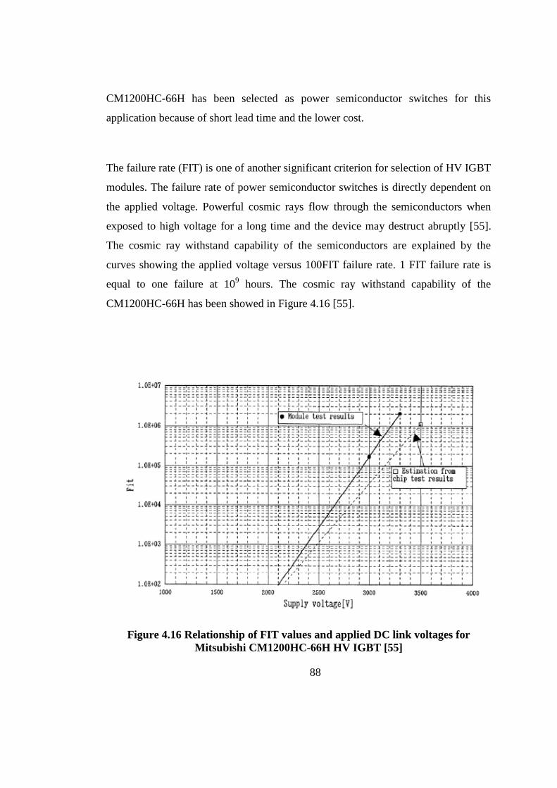
88
CM1200HC-66H has been selected as power semiconductor switches for this
application because of short lead time and the lower cost.
The failure rate (FIT) is one of another significant criterion for selection of HV IGBT
modules. The failure rate of power semiconductor switches is directly dependent on
the applied voltage. Powerful cosmic rays flow through the semiconductors when
exposed to high voltage for a long time and the device may destruct abruptly [55].
The cosmic ray withstand capability of the semiconductors are explained by the
curves showing the applied voltage versus 100FIT failure rate. 1 FIT failure rate is
equal to one failure at 109 hours. The cosmic ray withstand capability of the
CM1200HC-66H has been showed in Figure 4.16 [55].
Figure 4.16 Relationship of FIT values and applied DC link voltages for
Mitsubishi CM1200HC-66H HV IGBT [55]

89
It is seen that the DC link voltage at 100FIT is 2100V. FIT rate is increasing
drastically when exceeding this limit value. Therefore, 3300V, 1200A HV IGBTs
should not be exposed to the voltage over 2100V for all operating conditions to
extend their lifetime.
4.1.1.4 Optimization of IGBT Switching Waveforms
Figure 4.9-a in Subsection 4.1.1.2 has been used as the IGBT switching test circuitry
with the passive elements of Lstray=75nH, Rload=1Ω and Lload=200µH for HB units in
the laboratory. IGBT1 and IGBT 3 modules are turned off, and IGBT4 module is
turned on for the whole test duration. Consecutively, a turn-on signal of 1.2ms, a
turn-off signal of 30µs and second turn-on signal of 100µs have been applied to
IGBT2 module. During the first turn-on time, the current circulates through the path-
1 (DC link capacitors, IGBT4, Rload, Lload, IGBT2) and rises to a value of 2100A for
IGBT under a DC link voltage of 2100V. Applied turn-off signal to IGBT2 module,
the current flows through the diode part of IGBT1, D1 (current path-2) for a time of
30µs and then another turn-on signal is applied to IGBT2. Therefore, the turn-on and
turn-off waveforms are recorded for IGBT1 and IGBT2 modules. During the turn-on
of IGBT2 module, the reverse recovery characteristic of the inverse parallel diode of
IGBT1 is also obtained. Turn-on and turn-off performances of HV IGBT modules
used in the HB shown in Figure 4.8 are recorded in the laboratory by using the test
circuit in Figure 4.9-a.
The worst case in the transient state is taken to be the transition of the operating point
for T-STATCOM from full capacitive to full inductive or vice versa in nearly 80-
100ms. Moreover, if the standard IGBT driver circuit were not modified to prolong
the turn-on time to 2.5µs, IGBT module voltage and current waveforms would be as
in Figure 4.17 for the defined the worst case. By use of standard gate drive circuits,
diode reverse recovery current, Irr reaches 1500A and peak turn-on current of IGBT
tends to exceed 2400A. Although the actual SOAs are wider than those of datasheets

90
specified by the device manufacturer (APPENDIX-D), the use of a standard driver
circuit will shorten the economic life of HV IGBT modules. That is why the IGBT
driver circuit is modified in this research work.
Figure 4.17 The switching waveforms during turn-on of IGBT2 with standard
gate driver circuit at nearly Ic(rated)
For the purpose of the decreasing the Irr and hence peak turn-on currents of related
HV IGBT modules, the modification is made on the gate drive circuits by increasing
the turn-on control resistance, Rg(on) from 2.0 Ω to 3.2 Ω. After modifying gate
driver circuit, the turn-on time is found to be 2.5µs for HV IGBT modules. This
reduces reverse recovery current of anti-parallel diodes to Irr=1250A and hence peak
turn-on current of IGBT2 to 2250 A as shown in Figure 4.18 for the worst case in the
Sw
itc
hin
g W
av
efo
rms
of
IGB
T1
an
d IG
BT
2
-500
0
500
1000
1500
2000
2500
0 0.5 1.0 1.5 2.0 2.5 3.0 3.5 4.0 4.5 5.0
Time (µsec)
-1000
-1500
IGBT2 Module Current (A)
IGBT2 Module Voltage (V)
IGBT1 Module Current (A)
IGBT1 Module Voltage (V)Irr of D1
Peak Current
of IGBT2
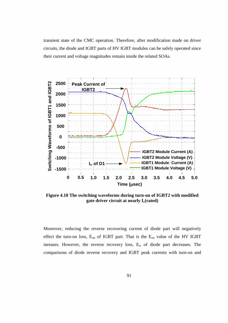
91
transient state of the CMC operation. Therefore, after modification made on driver
circuits, the diode and IGBT parts of HV IGBT modules can be safely operated since
their current and voltage magnitudes remain inside the related SOAs.
Figure 4.18 The switching waveforms during turn-on of IGBT2 with modified
gate driver circuit at nearly Ic(rated)
Moreover, reducing the reverse recovering current of diode part will negatively
effect the turn-on loss, Eon of IGBT part. That is the Eon value of the HV IGBT
inreases. However, the reverse recovery loss, Err of diode part decreases. The
comparisons of diode reverse recovery and IGBT peak currents with turn-on and
-500
0
500
1000
1500
2000
2500
0 0.5 1.0 1.5 2.0 2.5 3.0 3.5 4.0 4.5 5.0
-1000
-1500Sw
itc
hin
g W
av
efo
rms
of
IGB
T1
an
d IG
BT
2
IGBT2 Module Current (A)
IGBT2 Module Voltage (V)
IGBT1 Module Current (A)
IGBT1 Module Voltage (V)
Time (µsec)
Irr of D1
Peak Current of
IGBT2

92
reverse recovery losses for diode and IGBT parts of the modules have been given in
Table 4.1 for the use of standard and modified gate driver circuits.
Table 4.3 The comparison of diode reverse recovery and IGBT peak currents,
and turn-on and reverse recovery losses for IGBT modules
Although reverse recovery loss, Err of the diode part decreases by a percentage of
10.11%. the turn-on loss, Eon of the IGBT part increases by a percentage of 17.30%
as can be seen from Table 4.3.
4.1.1.5 Choice of DC Link Capacitor
In the DC link of each HB, low-ESR and -ESL power electronic capacitors are to be
used. In the design work, the variations in peak-to-peak ripple content of the
capacitor voltage, δVd against DC link capacitance are calculated by simulations and
the variations in δVd are given in Figure 4.19 when CMC is under CSS method for
the equalization of the DC link capacitor voltages of each HB unit. Among the DC
link equalization methods employed in this work, since it gives the maximum
percentage of peak-to-peak variation in DC link voltage for the same value of
capacitance as shown in Table 2.7 and Table 2.8 in Chapter-2, CSS method is
applied for the DC link capacitor voltage the equalization method for all simulations
The Parameters under investigation The use of Standard
Gate Driver Circuit
The use of Modified
Gate Driver Circuit
Turn-on Resistance, Rg(on)(Ω) 2.0 3.2
Diode Reverse Recorvery Current, Irr(A) 1500 1250
IGBT Peak Turn-on Current 2600 2250
Turn-on Loss, Eon (J/pulse) 2.08 2.44
Reverse Recovery Loss, Err (J/pulse) 0.69 0.62

93
carried out in this subsection as the worst case. Moreover, the total series filter
inductance has been taken as 3.53mH for the simulations.
For the chosen HV IGBT modules, the DC link voltage of each HB was taken to be
1900V DC. It is kept constant in the steady-state over the entire operating range of
the T-STATCOM by controlling the active power flow from the supply and also by
the DC link capacitor voltage equalization method applied to the CMC.
In view of the maximum allowable ripple content, 10% ripple content in DC link
voltage of 1900V is taken as a rule of thumb. Therefore, the DC link capacitance of
each HB is chosen to be 9.2mF to have peak-to-peak variations in DC link voltages
of the designed CMC lower than the specified limit both for inductive and capacitive
mode of operations as shown in Figure 4.19.
Figure 4.19 The variations in peak-to-peak voltage
ripple against capacitance value
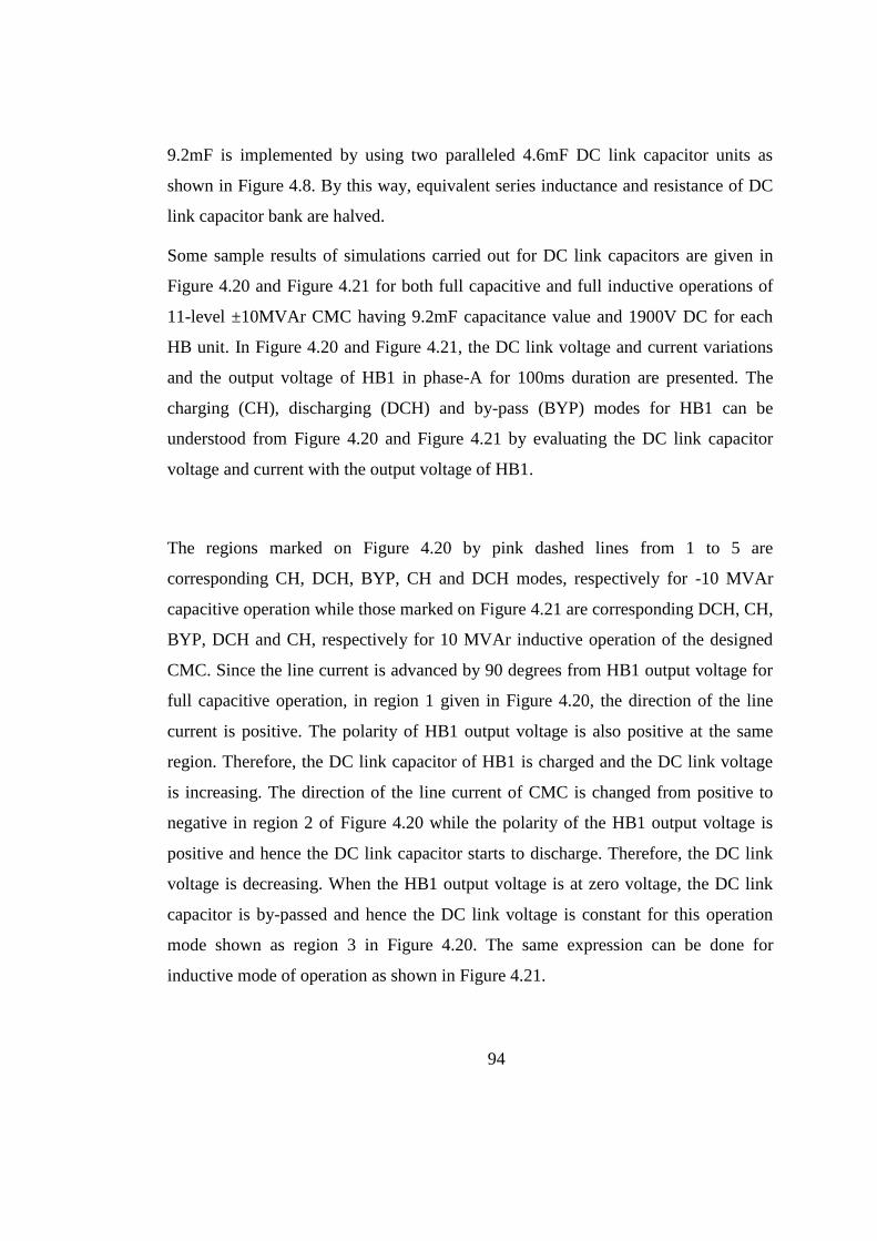
94
9.2mF is implemented by using two paralleled 4.6mF DC link capacitor units as
shown in Figure 4.8. By this way, equivalent series inductance and resistance of DC
link capacitor bank are halved.
Some sample results of simulations carried out for DC link capacitors are given in
Figure 4.20 and Figure 4.21 for both full capacitive and full inductive operations of
11-level ±10MVAr CMC having 9.2mF capacitance value and 1900V DC for each
HB unit. In Figure 4.20 and Figure 4.21, the DC link voltage and current variations
and the output voltage of HB1 in phase-A for 100ms duration are presented. The
charging (CH), discharging (DCH) and by-pass (BYP) modes for HB1 can be
understood from Figure 4.20 and Figure 4.21 by evaluating the DC link capacitor
voltage and current with the output voltage of HB1.
The regions marked on Figure 4.20 by pink dashed lines from 1 to 5 are
corresponding CH, DCH, BYP, CH and DCH modes, respectively for -10 MVAr
capacitive operation while those marked on Figure 4.21 are corresponding DCH, CH,
BYP, DCH and CH, respectively for 10 MVAr inductive operation of the designed
CMC. Since the line current is advanced by 90 degrees from HB1 output voltage for
full capacitive operation, in region 1 given in Figure 4.20, the direction of the line
current is positive. The polarity of HB1 output voltage is also positive at the same
region. Therefore, the DC link capacitor of HB1 is charged and the DC link voltage
is increasing. The direction of the line current of CMC is changed from positive to
negative in region 2 of Figure 4.20 while the polarity of the HB1 output voltage is
positive and hence the DC link capacitor starts to discharge. Therefore, the DC link
voltage is decreasing. When the HB1 output voltage is at zero voltage, the DC link
capacitor is by-passed and hence the DC link voltage is constant for this operation
mode shown as region 3 in Figure 4.20. The same expression can be done for
inductive mode of operation as shown in Figure 4.21.
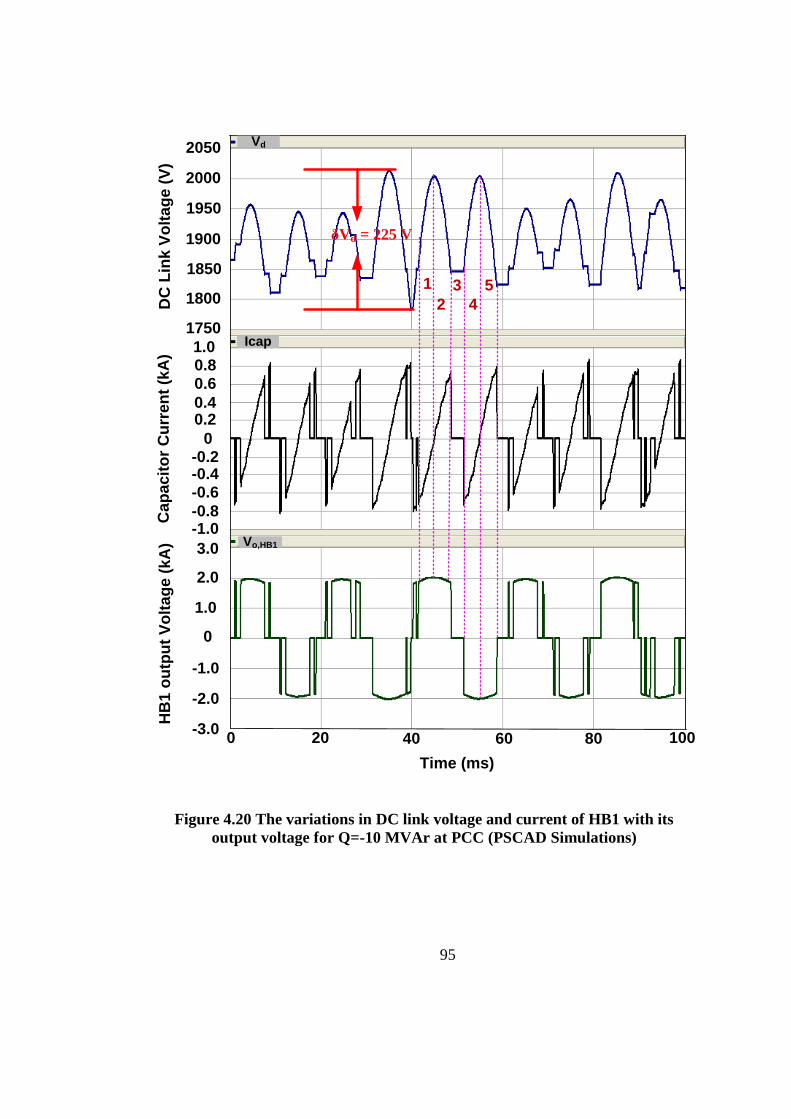
95
Figure 4.20 The variations in DC link voltage and current of HB1 with its
output voltage for Q=-10 MVAr at PCC (PSCAD Simulations)
Vd
Icap1750
1800
1850
1900
2000
2050
1950
DC
Lin
k V
olt
ag
e (
V)
0 20 40 60 80
Time (ms)
δVd = 225 V
-1.0-0.8
-0.6-0.4-0.2
0
0.20.4
0.60.81.0
Ca
pa
cit
or
Cu
rre
nt
(kA
)
-3.0
-2.0
-1.0
0
1.0
2.0
3.0
HB
1 o
utp
ut
Vo
lta
ge
(k
A) Vo,HB1
1 3
42
5
100

96
Figure 4.21 The variations in DC link voltage and current of HB1 with its
output voltage for Q=+10 MVAr at PCC (PSCAD Simulations)
Vd
Icap1825
1850
1875
1900
2000
2025
1950
DC
Lin
k V
olt
ag
e (
V)
0 20 40 60 80
Time (ms)
δVd = 180 V
-1.0-0.8
-0.6-0.4-0.2
0
0.20.4
0.60.81.0
Ca
pa
cit
or
Cu
rre
nt
(kA
)
-3.0
-2.0
-1.0
0
1.0
2.0
3.0
HB
1 o
utp
ut
Vo
lta
ge
(k
A) Vo,HB1
1 3 4
1925
1975
2
5
100

97
The peak-to-peak voltage variations for full inductive and full capacitive cases are
obtained as 225V and 180V, respectively as shown in Figure 4.22 and Figure 4.23.
In Figure 4.22 and Figure 4.23, the variations of harmonic content in DC link voltage
and current of HB1 in phase-A for 100ms duration are presented for both full
capacitive and full inductive operation modes.
Figure 4.22 The variations of harmonic components in DC link voltage and
current for Q=-10 MVAr at PCC (PSCAD Simulations)
Vd,dc
0
500
1000
1500
2000
DC
Lin
k V
olt
ag
e H
arm
on
ics
(V
)
0 20 40 60 80 100
Time (ms)
0
50
100
150
200
250
DC
Lin
k C
urr
en
t H
arm
on
ics
(A
)
Vd,1 Vd,2 Vd,3 Vd,4 Vd,5 Vd,6 Vd,7 Vd,8 Vd,9 Vd,10 Vd,11 Vd,12 Vd,13
Idc I1 I2 I3 I4 I5 I6 I7 I8 I9 I10 I11 I12 I13
300
350

98
Figure 4.23 The variations of harmonic components in DC link voltage and
current for Q=+10 MVAr at PCC (PSCAD Simulations)
The following conclusions have been found from the carried simulations for DC link
capacitor used in each HB circuit:
1) Although, the instantaneous DC link voltage exceeds 2000V, the mean DC
link voltage circulates around 1900V DC. Therefore, the choice of 2000V DC
mean for DC link capacitors is enough for the design. Also, a maximum true
rms current value of 475 A is obtained for full capacitive operation mode.
Vd,dc
0
500
1000
1500
2000
DC
Lin
k V
olt
ag
e H
arm
on
ics
(V
)
0 20 40 60 80 100
Time (ms)
0
50
100
150
200
250
DC
Lin
k C
urr
en
t H
arm
on
ics
(A
)
Vd,1 Vd,2 Vd,3 Vd,4 Vd,5 Vd,6 Vd,7 Vd,8 Vd,9 Vd,10 Vd,11 Vd,12 Vd,13
Idc I1 I2 I3 I4 I5 I6 I7 I8 I9 I10 I11 I12 I13
300
350

99
2) The peak-to-peak voltage value in DC link voltage at full capacitive operation
is δVd=225V which is higher than the obtained δVd=180 V for full inductive
Table 4.4 Current Harmonic Components seen in
DC link current for both full capacitive
and full inductive operation modes
Harmonic
Number
Full Capacitive
Currents (A)
Full Inductive
Currents (A)
1 78 77
2 370 252
3 66 34
4 140 30
5 19 48
6 102 16
7 60 49
8 25 47
9 48 67
10 64 60
11 39 66
12 129 43
13 18 35
14 75 17
15 14 31
16 4.5 28
17 10 17
18 27 6
19 7 15
20 58 21
21 6 15
22 51 28
23 8 18
24 28 7
25 12 5
26 5 22
27 12 16
28 38 12
29 14 8
30 55 16
31 14 5
TRUE
RMS
475 A 316 A

100
operation due to the higher modulation index. The same conclusion is true for
the peak-to-peak values of capacitor currents.
3) While the DC harmonic component is the highest one for the DC link
voltage, 2nd
harmonic component for the DC link current is the maximum
one, as expected. The voltage harmonic components other than DC are quite
low and can be disregarded.
4) Although the 2nd
harmonic current in DC link current is the highest for both
full capacitive and full inductive operation modes, some other components
apart from 2nd
harmonic component with relatively high magnitudes can also
be observed. Therefore, during the design of the DC link capacitors, these
harmonic components should also be considered when determining the rated
current value of DC link capacitors. Theese harmonic components in DC link
current up to 31 with true rms values for full capacitive and full inductive
operations have been listed in Table 4.4.
From carried out simulations, a pair of custom designed Metallized Polypropylene
Film (MKP) type DC link capacitors with ratings of 2000VDC, 4.6mF, 260A,rms
have been designed for each HB unit and produced by ELECTRONICON. These
MKP type DC capacitors are used for power electronics applications with nonlinear
currents and voltages with low equivalent self inductance (ESL) and equivalent
series resistance (ESR) values. The ESL value is very crucial for power
semiconductor switches due to peak voltages occurring during turn-off operations of
IGBT modules. The ESR value refers the losses of the capacitors. ESL and ESR
values are 50nH and 0.25mΩ for a unit of designed capacitor, respectively. Since a
pair of them is connected in parallel for each HB, these values halve to 25nH and
0.125 mΩ. Field test results given in Chapter-5 show that δVd does not exceed 9%
(170V) over the entire operating range of the T-STATCOM thus showing the success
of the choice of the DC link capacitance.

101
4.2 Design of Control System
The block diagram of the digital control system for a 154/10.5 kV, ±10MVAr T-
STATCOM based on an 11-level Cascaded Multilevel Converter is as shown in
Figure 4.24.
Figure 4.24 The block diagram of the digital control system of CMC with
control panel
11
5.2
kB
its/s
ec
RS
23
2
3 M
bit/s
ec
Industrial
Computer
11
5.2
kB
its/s
ec
SC
I
Comm.
Interface
Unit
19
.2k
Bits
/se
c
RS
48
5 C
om
m. L
ine
Dig
ital I/O
s
Digital
Interface
Unit
PLC
Dig
ital I/O
s
DSP Board
SP
I Co
mm
.
9.4
Mb
it/se
c
Dig
ital I/O
s
FPGA
Board
Protection
Relays
Power
Meter
Water
Cooling
System
Circuit
Breakers
RS485
Digital I/Os
19.2kBits/sec
CMC
DC_VM
DC_PD IGB
T G
ate
Dri
ve
rs
SC
I Co
mm
.
Dig
ital I/O
s
Fiber-Optic Cable Based Fiber-Optic Cable Based
Copper Wire Based Copper Wire Based
Communication Bus Digital I/O Bus
Commmunication Bus Digital I/O Bus
SC
I
External
Sub-Systems
PPI
19
.2k
Bits
/se
c
Ph-a,b,c / HB-1...n
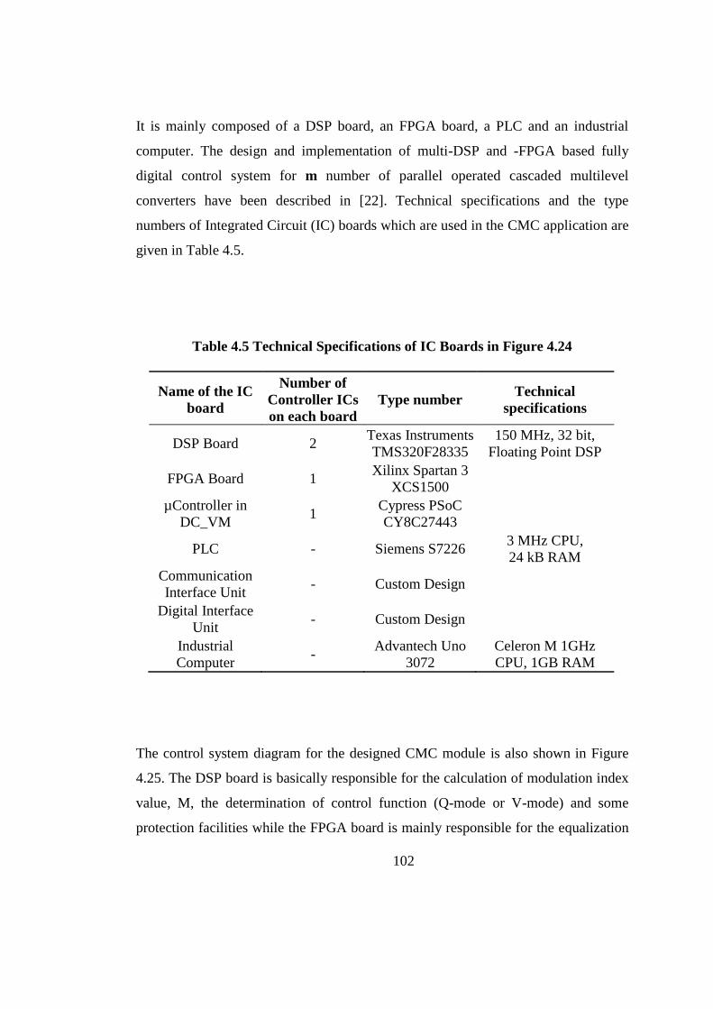
102
It is mainly composed of a DSP board, an FPGA board, a PLC and an industrial
computer. The design and implementation of multi-DSP and -FPGA based fully
digital control system for m number of parallel operated cascaded multilevel
converters have been described in [22]. Technical specifications and the type
numbers of Integrated Circuit (IC) boards which are used in the CMC application are
given in Table 4.5.
Table 4.5 Technical Specifications of IC Boards in Figure 4.24
The control system diagram for the designed CMC module is also shown in Figure
4.25. The DSP board is basically responsible for the calculation of modulation index
value, M, the determination of control function (Q-mode or V-mode) and some
protection facilities while the FPGA board is mainly responsible for the equalization
Name of the IC
board
Number of
Controller ICs
on each board
Type number Technical
specifications
DSP Board 2 Texas Instruments
TMS320F28335
150 MHz, 32 bit,
Floating Point DSP
FPGA Board 1 Xilinx Spartan 3
XCS1500
µController in
DC_VM 1
Cypress PSoC
CY8C27443
PLC - Siemens S7226 3 MHz CPU,
24 kB RAM
Communication
Interface Unit - Custom Design
Digital Interface
Unit - Custom Design
Industrial
Computer -
Advantech Uno
3072
Celeron M 1GHz
CPU, 1GB RAM

103
of DC link capacitor voltages, the determination of CSS or MSS method to applied
for equalization purpose and production of firing signals for IGBT modules used in
CMC as well as some protection facilities. The digital control system implemetation
of this work is applied by the project team as expressed in Acknowledgments.
Figure 4.25 The diagram of control system for the designed CMC module
PI+- MQload
(Vref)
Qstatcom
(Vpcc)
M
Vpcc
Limiter Modulation
Index
Block
Controller
Isupply ISTATCOM
DSP Board
Iconv
M
Limiter
M M
Phase Locked
Loop
Vpcc wt Iconv Idir
wt Idir
Selective
Swapping
Algorithm
Look-up
TableM Level
Generator
Switch
Firing
Unit Fir
ing
Sig
na
ls
PI +- Vdc,ref
Vdc,total
(Vdc,1+Vdc,2+…+Vdc,5)
Controller
Sign
Detector
FPGA
Board
θj HBj
wt ++
Limiter
Q-Mode V-Mode
δ
wt+δ CSS MSS
Idir
Firing Signals
154/10.5 kV
Coupling
Transformer
Power Grid
ST
AT
CO
M C
on
ve
rter+
++
++
C1
C2
C3
C4
C5
Vdc,1
Vdc,2
Vdc,3
Vdc,4
Vdc,5
Iconv
ISTATCOM
IsupplyPCC
Vpcc
Series Filter
Reactor

104
4.2.1.1 DSP Board
The DSP board contains two DSP chips: one for major control functions and serial
communication with PLC, while the other for major protection functions.
Operation mode of the T-STATCOM system is set by the operator and kept active by
the DSP Board . It can be operated in either reactive power compensation mode (Q-
mode) or terminal voltage regulation mode (V-mode) by using a selector switch as
shown in Figure 4.25.
Figure 4.26 Generation of Qref and Qc by DSP Board
Isupply
(isA,isB,isC)
DSP Board
vAB
ilC
vBC
ilAvCA
ibB
ql(k)
Σ1n
k = 1
n
Qload
(Qref)
ql(k)
isA
icA
ilA
isC
icC
ilC
isB
icB
ilB
vBf
vAfvAB
vCf
vBfvBC
vAf
vCfvCA
vAB
isC
vBC
isA
vCA
isB
qc(k)
Σ1n
k = 1
n
Qcqc(k)
IIR
IIR
IIR
Lead &
Lag
Comp.
Lead &
Lag
Comp.
Lead &
Lag
Comp.
vAN
vBN
vCN
vANf
vBNf
vCNf
LPF
LPF
LPF
IT-STATCOM
(icA,icB,icC)
VPCC
(VAN,VBN,VCN)
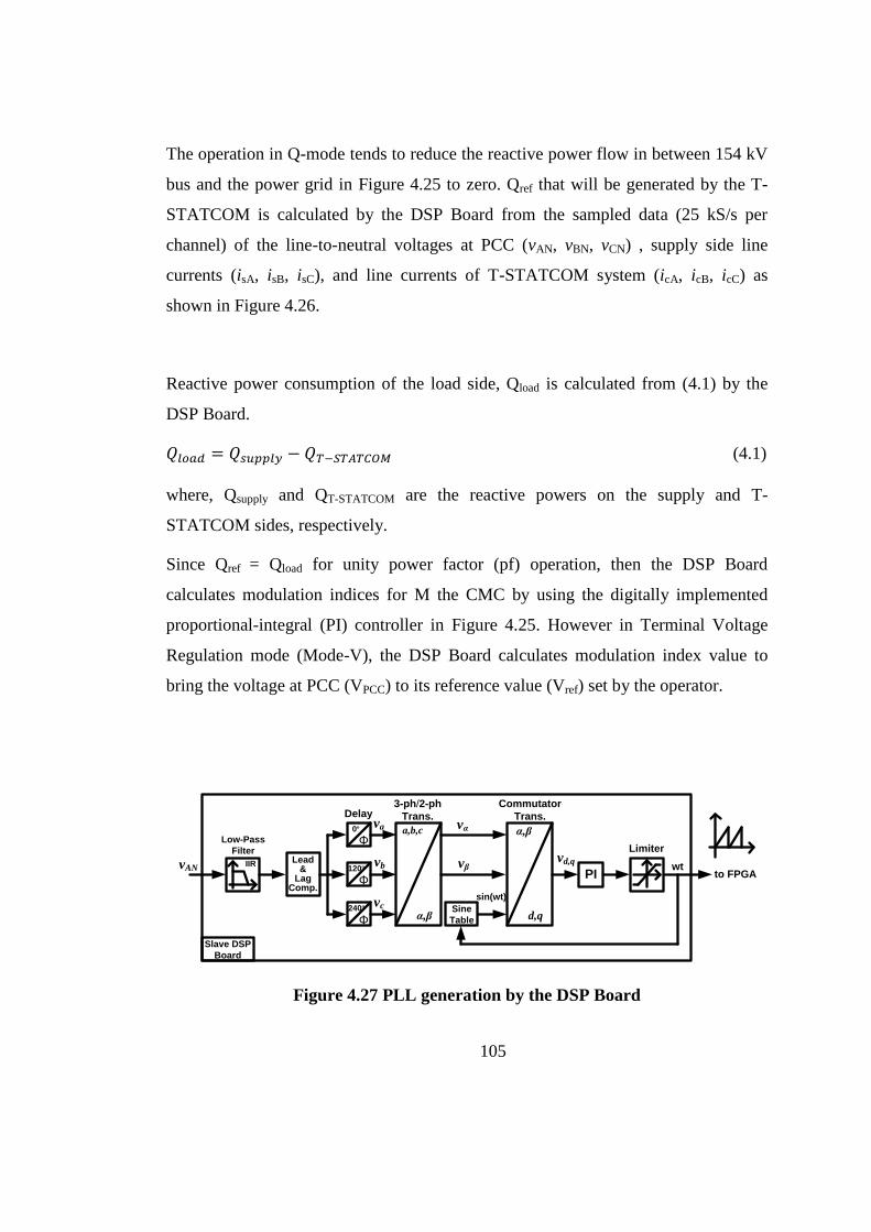
105
The operation in Q-mode tends to reduce the reactive power flow in between 154 kV
bus and the power grid in Figure 4.25 to zero. Qref that will be generated by the T-
STATCOM is calculated by the DSP Board from the sampled data (25 kS/s per
channel) of the line-to-neutral voltages at PCC (vAN, vBN, vCN) , supply side line
currents (isA, isB, isC), and line currents of T-STATCOM system (icA, icB, icC) as
shown in Figure 4.26.
Reactive power consumption of the load side, Qload is calculated from (4.1) by the
DSP Board.
(4.1)
where, Qsupply and QT-STATCOM are the reactive powers on the supply and T-
STATCOM sides, respectively.
Since Qref = Qload for unity power factor (pf) operation, then the DSP Board
calculates modulation indices for M the CMC by using the digitally implemented
proportional-integral (PI) controller in Figure 4.25. However in Terminal Voltage
Regulation mode (Mode-V), the DSP Board calculates modulation index value to
bring the voltage at PCC (VPCC) to its reference value (Vref) set by the operator.
Figure 4.27 PLL generation by the DSP Board
Slave DSP
Board
IIR Lead&
Lag Comp.
Φ120º
Φ0º
Φ240º
va
vb
vc
a,b,c
α,β
vα
vβ
α,β
d,q
PI
Limitervd,q
wt
Low-Pass
Filter
Delay3-ph/2-ph
Trans.
Commutator
Trans.
Sine
Table
sin(wt)
vANto FPGA
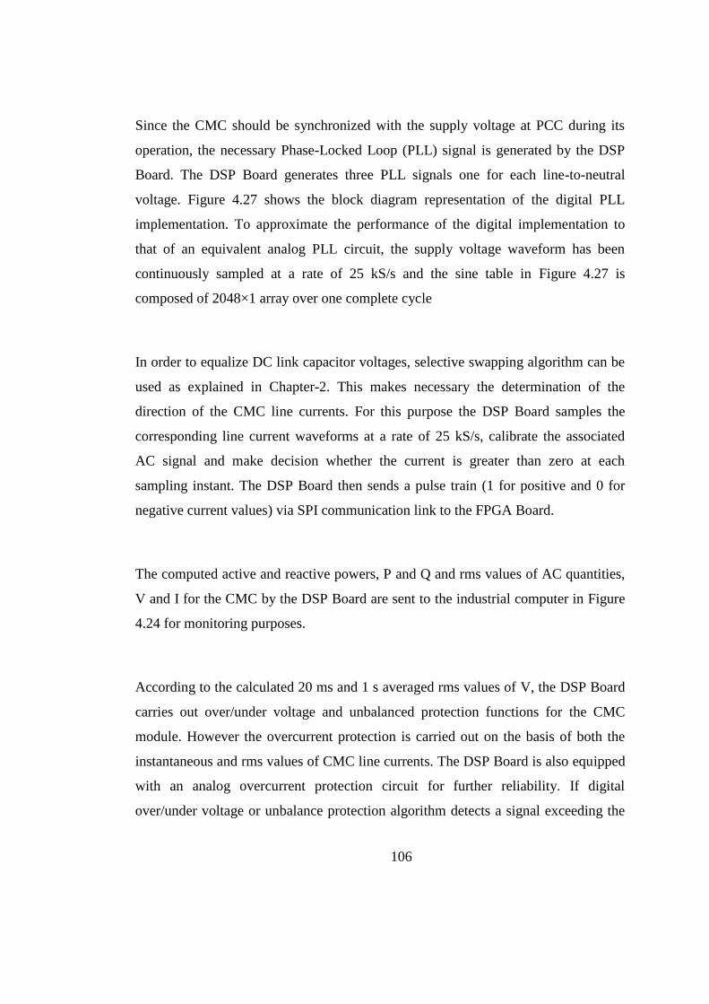
106
Since the CMC should be synchronized with the supply voltage at PCC during its
operation, the necessary Phase-Locked Loop (PLL) signal is generated by the DSP
Board. The DSP Board generates three PLL signals one for each line-to-neutral
voltage. Figure 4.27 shows the block diagram representation of the digital PLL
implementation. To approximate the performance of the digital implementation to
that of an equivalent analog PLL circuit, the supply voltage waveform has been
continuously sampled at a rate of 25 kS/s and the sine table in Figure 4.27 is
composed of 2048×1 array over one complete cycle
In order to equalize DC link capacitor voltages, selective swapping algorithm can be
used as explained in Chapter-2. This makes necessary the determination of the
direction of the CMC line currents. For this purpose the DSP Board samples the
corresponding line current waveforms at a rate of 25 kS/s, calibrate the associated
AC signal and make decision whether the current is greater than zero at each
sampling instant. The DSP Board then sends a pulse train (1 for positive and 0 for
negative current values) via SPI communication link to the FPGA Board.
The computed active and reactive powers, P and Q and rms values of AC quantities,
V and I for the CMC by the DSP Board are sent to the industrial computer in Figure
4.24 for monitoring purposes.
According to the calculated 20 ms and 1 s averaged rms values of V, the DSP Board
carries out over/under voltage and unbalanced protection functions for the CMC
module. However the overcurrent protection is carried out on the basis of both the
instantaneous and rms values of CMC line currents. The DSP Board is also equipped
with an analog overcurrent protection circuit for further reliability. If digital
over/under voltage or unbalance protection algorithm detects a signal exceeding the

107
pre-specified limits, an alarm signal will be generated and sent to FPGA to turn off
IGBTs. On the other hand, if the digital overcurrent algorithm detects a signal
exceeding pre-specified limits, a trip signal will be generated and sent to the Circuit
Breakers (CB) to isolate the T-STATCOM system and the associated FPGA to turn
off the IGBT modules of the CMC.
4.2.1.2 FPGA Board
FPGA Board is composed of an FPGA chip, a multiplexer circuit, fiber optic
transmitters/receivers and other peripheral devices. The major functions of the FPGA
board can be summarized as follows:
a. CMC losses are compensated by allowing active power flow from the supply
to the T-STATCOM system. Active power flow is controlled by load angle,
δ. To control the value of δ, FPGA Board first compares total DC link voltage
Vdc of the CMC with its reference value, then processes the error signal with
a PI controller as shown in Figure 4.25. This means that, the AC voltage
waveform synthesized by the FPGA should be shifted by δ with respect to
supply voltage at PCC. Therefore, the PLL signal sent by the DSP Board
should be shifted by angle δ during the implementation of the active power
control by the FPGA Board. To improve the waveform synthesizing task, the
discrete PLL signal is approximated to a continuous signal by applying linear
interpolation technique.
b. The optimum angles θ1,θ2,…,θ5 according to SHEM are calculated off-line as
a function of M and then stored in the memory of the FPGA in a look-up
table (204x6 matrix). The FPGA board extracts optimum angles from look-up
table once for every 40µs period by using M value sent by the control DSP
chip.
c. The DC link capacitor voltages are equalized by using MSS method during
the operation of the CMC. This will be achieved by FPGA board by using

108
current direction signal sent by protection DSP chip, and the instantaneous
DC link capacitor voltage signals sent by the DC_VM circuit.
d. Upon the request of control DSP chip, the FPGA board creates the necessary
turn-on and turn-off signals for IGBTs to charge the DC link capacitors
successfully during the pre-charging period. Upon the request of the PLC, the
FPGA board discharges the capacitors by activating the DC_PD circuit in
Figure 4.24. Each DC_PD Board is composed of power stage of a chopper
circuit supplying controlled power to an external discharge resistor and an
analog protection circuit. DC_PD Board receives controlled duty ratio signals
from FPGA in order to keep the power dissipation of the discharge resistor
constant during the discharge period.
e. A smooth transition between different Q or V settings is aimed at the design
of the control system. This will minimize the oscillations in current, voltage
and reactive power in transition periods and hence reduce the settling time.
The extreme operating condition is the transition from full capacitive to full
inductive operation mode, or vice versa. For this purpose, first, the changes in
the modulation index have been applied only at zero crossing points of the
CMC line current by the FPGA Board.
FPGA board also carries out some protection functions such as short circuit
protection of IGBTs, over temperature, overvoltage protection of DC link capacitors,
etc..
4.2.1.3 Programmable Logic Controller (PLC)
The Programmable Logic Controller (PLC) in Figure 4.24 achieves control actions
according to the signals received from the DSP Board and external sub-systems via
digital/analog I/Os and data acquisition and state monitoring actions received from

109
the same system elements via serial communication channels. The major operational
features of the PLC are as described below:
a. The PLC carries out data acquisition, state monitoring and fault diagnosis
actions according to the signals taken from the DSP Board and external sub-
systems.
b. The operation state of the T-STATCOM system (on/off operation of circuit-
breakers and the load-break switch) is commanded by the PLC according not
only to the protection signals received from the de-ionized water cooling
system but also to on/off or protective signals received from other system
elements.
c. Remote control signals can be actuated by the PLC.
d. Some of the fault/failure signals are received from other control system
elements and then classified by the PLC for the activation of automatic re-
closing system. The de-ionized water cooling system is therefore turned on by
the PLC before re-closing action of the main CB to provide cooling service
for power semiconductors. The classified and unclassified fault/failure data
are also sent to the industrial computer in Figure 4.24 for monitoring purpose.
4.3 Switching Strategies for the Application of Selective
Swapping
In this work, the switching strategy chosen in the application of both CSS and MSS
causes voltage spikes with magnitudes ±Vd, ±2Vd, ±3Vd and ±4Vd superimposed on
the 11-level line-to-neutral voltage waveform as given in Figure 4.6. As an example,
in Figure 4.6 the voltage spike marked by vs1 can be explained by the aid of Figure
4.28 which is drawn for the three transition modes of CMC phase-A. Initially, line-
to-neutral voltage is, +4Vd and the status of the switches are as marked in Figure
4.28 by Mode-1. At the MSS instant (∆ts=400µs), interchange HB5 by HB4 by
turning off both IGBT4 module of HB5 and IGBT3 module of HB4 and at the same
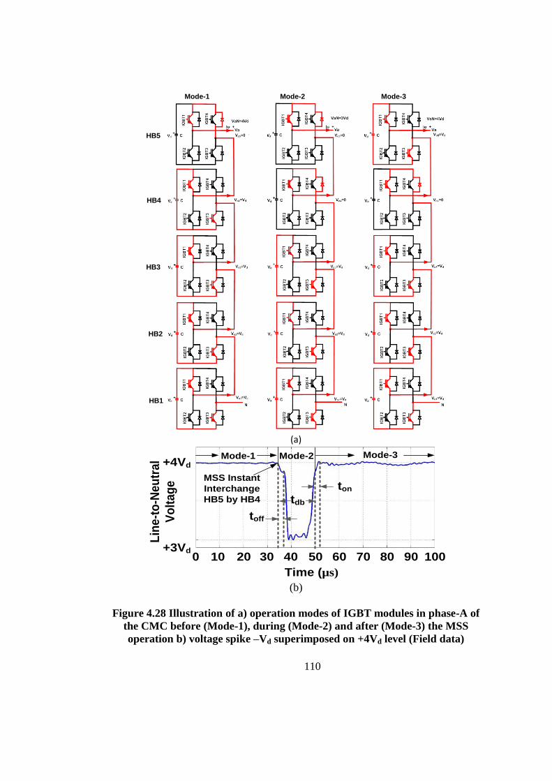
110
(a)
(b)
Figure 4.28 Illustration of a) operation modes of IGBT modules in phase-A of
the CMC before (Mode-1), during (Mode-2) and after (Mode-3) the MSS
operation b) voltage spike –Vd superimposed on +4Vd level (Field data)
Mode-1 Mode-2 Mode-3
HB5
HB4
HB3
HB2
HB1
0 10 20 30 40 50 60 70 80 90 100
Time (µs)
+3Vd
+4Vd
toff
tdb
ton
Mode-2 Mode-3Mode-1
MSS Instant
Interchange
HB5 by HB4
Lin
e-t
o-N
eu
tra
l
Vo
lta
ge

111
time initialize the dead-band period (tdb=13µs). This operation mode is illustrated by
Mode-2 in Figure 4.28. When IGBT3 module in HB4 is successfully turned off, the
negative AC current of HB4 starts to circulate through anti-parallel diode of IGBT4
module of HB4 resulting in BYP mode. At the end of the dead-band period, both
IGBT3 module of HB5 and IGBT4 module of HB4 are turned on resulting in DCH
mode for HB5. This operation mode is illustrated by Mode-3 in Figure 4.28.
The switching strategy described above causes a drop in line-to-neutral voltage
waveform from +4Vd to +3Vd and back to +4Vd for a period of nearly 15.5µs owing
to the operation of the incoming HB5. If the MSS operation takes place on ±3Vd
voltage level of line-to-neutral voltage waveform, depending upon the number of
incoming HBs, either ±Vd or ±2Vd voltage spike will be superimposed on the voltage
waveform. Similarly, MSS operations on ±2Vd and ±Vd may yield voltage spikes
either of ±Vd, ±2Vd, ±3Vd and ±Vd, ±2Vd, ±3Vd, ±4Vd, respectively.
An alternative switching strategy can reduce only the duration of voltage spikes to
turn-off time of IGBTs at the expense of a more complex control algorithm. This can
be achieved by sending the turn-off signal to the gate of the IGBT of outgoing HB
just at the end of the dead-band period. It is worth to note that these voltage spikes
can not reflect to PCC since they are successfully absorbed by the input filter reactor
of the CMC.
At the transition instants from 0 to ±Vd voltage level of line-to-neutral voltage
waveform, always a voltage spike of ±4Vd is superimposed on 0 voltage level
(Figure 4.6). As an example, in Figure 4.6 the voltage spike marked by vs2 can be
explained by the aid of Figure 4.29 which is drawn for the three transition modes of
CMC phase-A. In Mode-1 of Figure 4.29, all HBs are operating in BYP mode
resulting in 0 line-to-neutral voltage. In order to produce +Vd voltage level in the
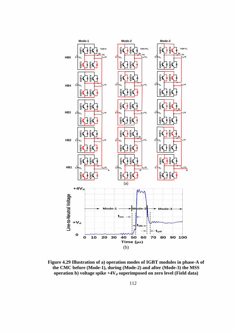
112
(a)
(b)
Figure 4.29 Illustration of a) operation modes of IGBT modules in phase-A of
the CMC before (Mode-1), during (Mode-2) and after (Mode-3) the MSS
operation b) voltage spike +4Vd superimposed on zero level (Field data)
N
Vo5=0
IoIGB
T1
IGB
T2
IGB
T4
IGB
T3
+C Vd
Vo4=0
IGB
T1
IGB
T2
IGB
T4
IGB
T3
+C Vd
Vo3=0
IGB
T1
IGB
T2
IGB
T4
IGB
T3
+C Vd
Vo2=0
IGB
T1
IGB
T2
IGB
T4
IGB
T3
+C Vd
Vo1=0
IGB
T1
IGB
T2
IGB
T4
IGB
T3
+C Vd
Va
VaN=0
Vo5=Vd
Vo4=Vd
Vo3=Vd
Vo2=Vd
Vo1=0
IGB
T1
IGB
T2
IGB
T4
IGB
T3
+C Vd
Va
VaN=4Vd
+C
IoIGB
T1
IGB
T2
IGB
T4
IGB
T3
Vd
+C
IGB
T1
IGB
T2
IGB
T4
IGB
T3
Vd
+C
IGB
T1
IGB
T2
IGB
T4
IGB
T3
Vd
+C
IoIGB
T1
IGB
T2
IGB
T4
IGB
T3
Vd
N
Mode-1 Mode-2 Mode-3
Vo5=0
Vo4=0
Vo3=0
Vo2=0
Vo1=Vd
IGB
T1
IGB
T2
IGB
T4
IGB
T3
+C Vd
Va
VaN=Vd
N
Io+
C
IGB
T1
IGB
T2
IGB
T4
IGB
T3
Vd
+C
IGB
T1
IGB
T2
IGB
T4
IGB
T3
Vd
Io+
C
IGB
T1
IGB
T2
IGB
T4
IGB
T3
Vd
Io+
C
IGB
T1
IGB
T2
IGB
T4
IGB
T3
Vd
HB5
HB4
HB3
HB2
HB1
0 10 20 30 40 50 60 70 80 90 100
Time (µs)
0
+4Vd
toff
tdb
ton
Mode-2 Mode-3Mode-1
+Vd
Line
-to-N
eutra
l Vol
tage
113
line-to-neutral voltage waveform, operation mode of HB1 is to be switched from
BYP mode to CH mode as illustrated in Mode-3 of Figure 4.29. This is achieved by
turning off IGBT2s and IGBT3s of HB2 to HB5 and at the same time IGBT2 of
HB1. Therefore, in Mode-2 of Figure 4.29, HBs from 2 to 5 produces a voltage spike
of +4Vd. At the end of dead-band period, IGBT1 of HB1, and IGBT2s and IGBT3s
of the remaining four HBs is turned on resulting +Vd voltage level in line-to-neutral
voltage waveform.
This switching strategy is preferred in order to equalize the utilization of IGBT
modules and to simplify the switching algorithm. In summary, this switching
strategy is applied by monitoring the zero crossings of the voltage waveforms by the
use PLL circuit and thus producing +4Vd voltage spike at the transition instant from
0 to +Vd on the positive half cycle and -4Vd at the transition from 0 to -Vd on the
negative half cycle for capacitive operation mode. The reverse is true for inductive
mode of operation.
An alternative to the above switching strategy is to monitor the line currents of CMC
instead of line to neutral voltage waveforms. On the negative half cycle of the CMC
current, IGBT2 of HB1 (Mode-1) is turned off and after dead-band period IGBT1 of
HB1 is turned on. This switching strategy will eliminate Mode-2 on Figure 4.29 and
associated voltage spike. This switching strategy may fail when CMC is producing
very small amounts of reactive power and hence fundamental current owing to the
presence of 17th
and 19th
current harmonic components.
A better but more complex switching strategy can be recommended based on the
line-to-neutral voltage waveforms and hence PLL signals. In this method, one
complete cycle of the voltage waveform is to be divided into two parts from π/2 to
3π/2 and from 3π/2 to 5π/2 and applying switchings at the positive peak and negative

114
peak of the line-to-neutral voltage waveforms for changing by-pass modes instead
zero crossing points. This strategy will eliminate ±4Vd voltage spikes in Figure 4.29.
115
CHAPTER 5
THE IMPLEMENTATION OF T-STATCOM SYSTEM
AND
FIELD PERFORMANCE RESULTS
5.1 The Implementation of T-STATCOM System
In this research and technology development work, a 154 kV, ±50 MVAr, H-Brdige
(HB) based Multilevel T-STATCOM composed of five 12 kV, ±12 MVAr Cascaded
Multilevel Converter (CMC) designed in Chapter 4 has been implemented primarily
for the purposes of reactive power compensation and terminal voltage regulation, and
secondarily for power system stability. Figure 5.1 shows the schematic diagram of
the implemented 154 kV, ±50 MVAr T-STATCOM system. Five 12 kV, ±12 MVAr
Cascaded Multilevel Converter (CMC) modules are connected in parallel via air-core
reactors. The combination of these five CMC modules is then connected to 154 kV
bus via a 154/10.5 kV, 50/62.5 MVA, Y-Y connected coupling transformer. The
neutral point of the primary is solidly grounded while that of the secondary is
grounded via a 6.93Ω grounding resistor to limit line-to-ground fault current to 1 kA.
The T-STATCOM system is equipped with a digital control system which uses the
basic control architecture described in Chapter 4 for an CMC. The only difference is
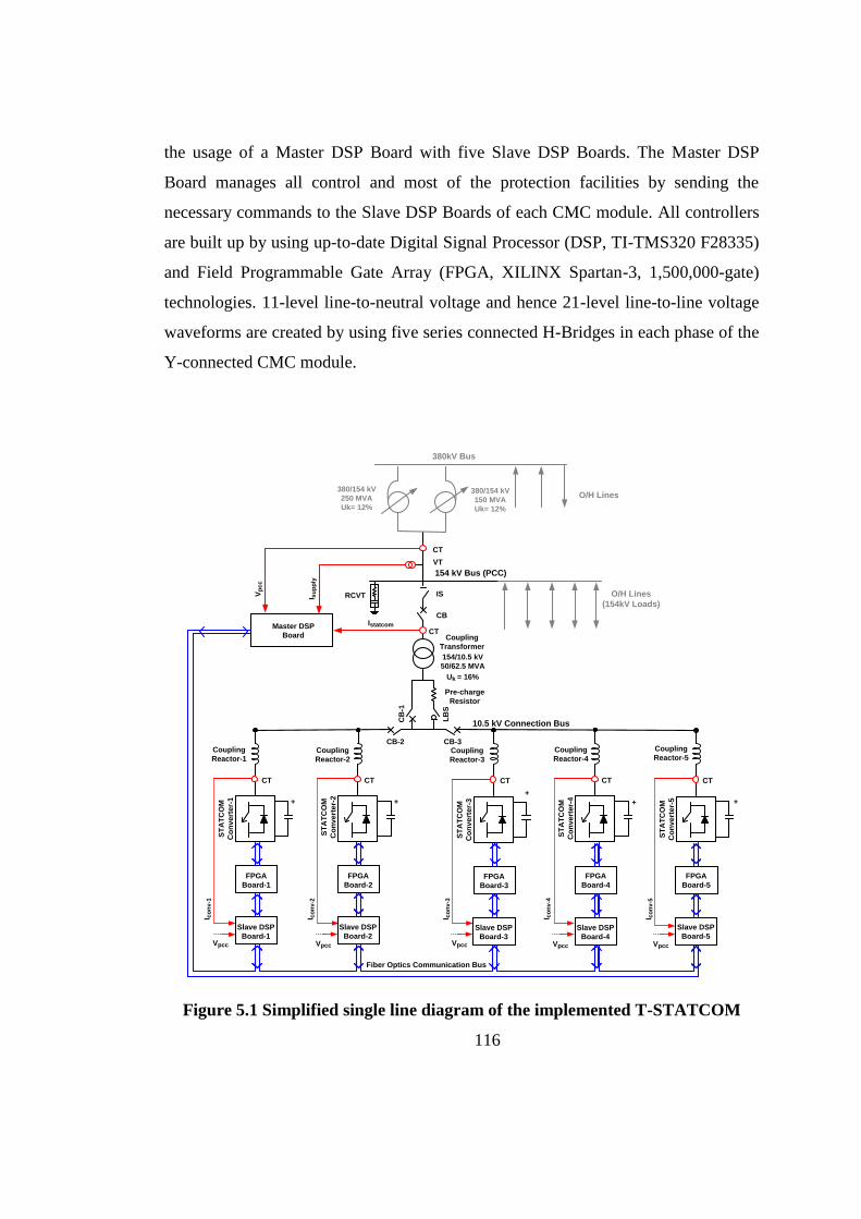
116
the usage of a Master DSP Board with five Slave DSP Boards. The Master DSP
Board manages all control and most of the protection facilities by sending the
necessary commands to the Slave DSP Boards of each CMC module. All controllers
are built up by using up-to-date Digital Signal Processor (DSP, TI-TMS320 F28335)
and Field Programmable Gate Array (FPGA, XILINX Spartan-3, 1,500,000-gate)
technologies. 11-level line-to-neutral voltage and hence 21-level line-to-line voltage
waveforms are created by using five series connected H-Bridges in each phase of the
Y-connected CMC module.
Figure 5.1 Simplified single line diagram of the implemented T-STATCOM
CT
VT
154/10.5 kV
50/62.5 MVA
Uk = 16%
Coupling
Transformer
10.5 kV Connection Bus
Pre-charge
Resistor
LB
S
Fiber Optics Communication Bus
CB
-1
CB-2 CB-3
154 kV Bus (PCC)
Master DSP
Board
CT
O/H Lines
(154kV Loads)
Vp
cc
I su
pp
ly
Istatcom
380kV Bus
IS
CB
380/154 kV
250 MVA
Uk= 12%
380/154 kV
150 MVA
Uk= 12%
O/H Lines
Coupling
Reactor-5
ST
AT
CO
M
Co
nv
ert
er-
5
CT
+
FPGA
Board-5
Slave DSP
Board-5
I co
nv
-5
Vpcc
Coupling
Reactor-4
ST
AT
CO
M
Co
nv
ert
er-
4
CT
FPGA
Board-4
Slave DSP
Board-4
I co
nv
-4
Vpcc
+
Coupling
Reactor-1
ST
AT
CO
M
Co
nv
ert
er-
1
CT
+
FPGA
Board-1
Slave DSP
Board-1
I co
nv
-1
Vpcc
Coupling
Reactor-3
ST
AT
CO
M
Co
nv
ert
er-
3
CT
+
FPGA
Board-3
Slave DSP
Board-3
I co
nv
-3
Vpcc
Coupling
Reactor-2
ST
AT
CO
M
Co
nv
ert
er-
2
CT
+
FPGA
Board-2
Slave DSP
Board-2
I co
nv
-2
Vpcc
RCVT

117
The developed 154kV, ±50 MVAr T-STATCOM system has been installed in 380
kV/154 kV Sincan Transformer Substation, Ankara as shown in Figure 5.2. Table 5.1
summarizes the technical specifications of each HB, CMC module and the resulting
T-STATCOM system. The coupling transformer (ONAN/ONAF), high voltage (HV)
and medium voltage (MV) switchgear equipment, input filter reactors and the water-
Table 5.1 The technical specifications of
the installed T-STATCOM system
T-STATCOM
Rated Power ±50 MVAr
Rated Voltage 154 kV
Coupling Transformer Y-Y, 154/11.1 kV,
50/62.5 MVA, 16% uk
Number of CMC Modules in Parallel 5
Cascaded Multilevel Converters (CMC)
Rated Power ±12 MVAr
Rated Voltage 10.5 kV (max.12kV)
Number of H-Bridges per phase 5
Number of Levels in Voltages 11 Levels Line-to-Neutral,
21 Levels Line-to-Line
Harmonics Eliminated by SHEM 5th
, 7th
, 11th
, 13th
Coupling Reactors 2.5mH, air core
Cooling System De-ionized water cooling
H-Bridges (HB)
Rated Power ±840 kVAr
Rated Voltage 1.8 kV rms
Power Semiconductor 3300V, 1200A HV IGBT with
parallel inverse diode
Effective Switching Frequency 500Hz
Design Value of DC Link Voltage 1900Vdc
DC Link Capacitor*
*Metallized Polypropylene (MKP)
9.2mF (4.6mF//4.6mF) ±10%
260A rms, 2000Vdc
250V peak-to-peak ripple

118
(a)
(b)
(c)
(d)
Figure 5.2 154 kV, ±50 MVAr T-STATCOM based on 11-level CMC installed at
380kV/154kV Sincan Transformer Substation
((a) Interior view of trailer with power stages, (b) Control cabinets, (c) Trailer
for ±50 MVAr T-STATCOM on road (WxLxH:3700mmx16800mmx4300mm),
and (d) General view of T-STATCOM)
119
to-air heat exchanger of this system are installed outdoor (Figure 5.2-d). The power
stages of five CMC modules, the control system cabinets and part of the de-ionized
water cooling system excluding water-to-air heat exchanger are placed into a non-
magnetic container mounted on a trailer (Figure 5.2-c). This makes possible easy
relocation of the T-STATCOM to another problematic point of the transmission
system whenever this is required.
5.1.1 Power System Characteristics
This subsection describes the electrical power system characteristics of the 154 kV
Point of Common Coupling (PCC) transmission bus at which the implemented
154kV, ±50MVAR T-STATCOM system is connected at Sincan Transformer
Substation, Ankara before installation of the system. The PCC side electrical
characteristics are given in Table 5. 2. The maximum SCMVA value is around
5300MVA at 154kV for PCC and the corresponding 3-phase solidly short circuit
current is 19.87 kA at rated voltage.
Table 5. 2 The electrical characteristics of the power system
at which T-STATCOM system is connected
Nominal Voltage 154 kV
Maximum Voltage 170 kV
Short Circuit Level (SCMVA) 5300MVA at 154 kV
Many overhead (O/H) lines longer than 100 km length in around Ankara are
connected to the 154kV bus at which the T-STATCOM system has been connected.
In the daytimes, the reactive power variation of the PCC is generally inductive-
reactive due to industrial loads fed by the O/H lines while during the nighttime the

120
variation in the reactive power changes to the capacitive-reactive due to Ferranti
Effect of the O/H lines because of light load condition.
Some measurements have been taken continuously from November of 2008 to June
of 2009 by the high accurate class Power Quality (PQ) analyzers. The all electrical
parameters of the power system described in this subsection are measured according
to IEC 61000-4-30 standard [56]. The variations in the reactive power and line-to-
neutral voltages of 154 kV bus are shown in Figure 5.3 and Figure 5.4. Also, the
maximum monthly inductive-reactive and capacitive-reactive variations from
November of 2008 to June of 2009 have also listed in Table 5.3. From Table 5.3, it is
obvious that the variations in the reactive power at PCC are between 60 MVAr
inductive-reactive and -40 MVAr capacitive-reactive in the year of 2009 before the
installation of the T-STATCOM system. Therefore, at least five 12kV, ±12MVAr
CMC modules should be operated in parallel to have +60MVAr inductive-reactive
and -40MVAr capacitive-reactive power. As can be seen from the Figure 5.4, the
line-to-neutral voltage of the PCC is over 89kV (root three of 154 kV) almost for the
whole measurement time period.
Figure 5.3 The variations in reactive power per phase at PCC side (Nov.2008-
June.2009, field data)
-15
-10
-5
0
5
10
15
20
25
Re
ac
tiv
e P
ow
er
(MV
Ar)
17.11.2008
11:59:17
06.01.2009
11:59:17
16.04.2009
11:59:17
25.02.2009
11:59:17
01.06.2009
11:59:17
Qa Qb Qc
Time

121
Figure 5.4 The variations in PCC side line-to-neutral voltages (Nov.2008-
June.2009, field data)
Table 5.3 The monthly maximum reactive power
variations of the PCC from Nov.2008 to June.2009
This is because of the dynamic operation of tap changers installed for
autotransformers used in the substation and the high SCMVA value of the PCC.
Therefore, the need of voltage regulation for the PCC is not needed so much for HV
PCC bus. However, to show effectiveness of T-STATCOM on voltage regulation,
Voltage Regulation Mode (V-Mode) is also inserted into the digital control of T-
STATCOM.
01.06.2009
11:59:17
88
89
90
91
92
93
94
95
96
PC
C L
ine
-to
-Ne
utr
al V
olt
ag
e (
kV
)
17.11.2008
11:59:17
06.01.2009
11:59:17
16.04.2009
11:59:17
25.02.2009
11:59:17
Time
Van Vbn Vcn
Time Max. Inductive
Reactive Power
Max. Inductive
Reactive Power
November 2008 +48 MVAr -22 MVAr
December 2008 +50 MVAr -25 MVAr
January 2009 +50 MVAr -22 MVAr
February 2009 +50 MVAr -27 MVAr
March 2009 +60 MVAr -27 MVAr
April 2009 +50 MVAr -35 MVAr
May 2009 +15 MVAr -40 MVAr
June 2009 +20 MVAr -30 MVAr
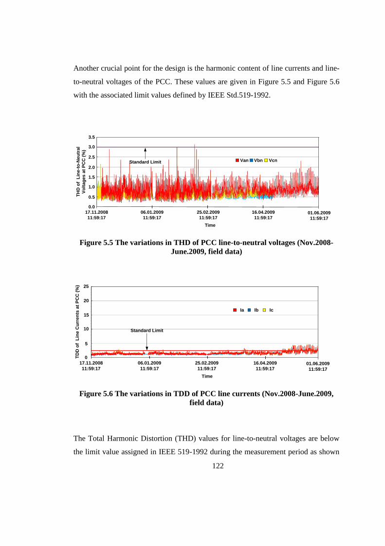
122
Another crucial point for the design is the harmonic content of line currents and line-
to-neutral voltages of the PCC. These values are given in Figure 5.5 and Figure 5.6
with the associated limit values defined by IEEE Std.519-1992.
Figure 5.5 The variations in THD of PCC line-to-neutral voltages (Nov.2008-
June.2009, field data)
Figure 5.6 The variations in TDD of PCC line currents (Nov.2008-June.2009,
field data)
The Total Harmonic Distortion (THD) values for line-to-neutral voltages are below
the limit value assigned in IEEE 519-1992 during the measurement period as shown
0.0
0.5
1.0
1.5
2.0
2.5
3.0
3.5
TH
D o
f L
ine
-to
-Ne
utr
al
Vo
lta
ge
s a
t P
CC
(%
)
17.11.2008
11:59:17
06.01.2009
11:59:17
16.04.2009
11:59:17
25.02.2009
11:59:17
Time
Van Vbn Vcn
01.06.2009
11:59:17
Standard Limit
0
5
10
15
20
25
TD
D o
f L
ine
Cu
rre
nts
at
PC
C (
%)
17.11.2008
11:59:17
06.01.2009
11:59:17
16.04.2009
11:59:17
25.02.2009
11:59:17
Time
Ia Ib Ic
01.06.2009
11:59:17
Standard Limit
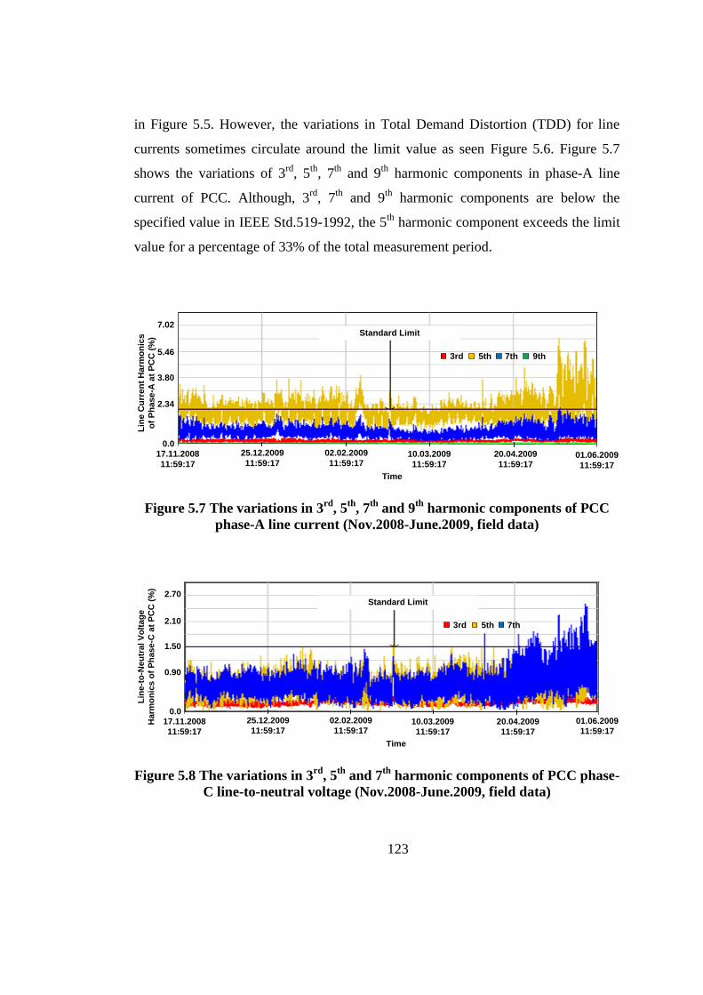
123
in Figure 5.5. However, the variations in Total Demand Distortion (TDD) for line
currents sometimes circulate around the limit value as seen Figure 5.6. Figure 5.7
shows the variations of 3rd
, 5th
, 7th
and 9th
harmonic components in phase-A line
current of PCC. Although, 3rd
, 7th
and 9th
harmonic components are below the
specified value in IEEE Std.519-1992, the 5th
harmonic component exceeds the limit
value for a percentage of 33% of the total measurement period.
Figure 5.7 The variations in 3rd
, 5th
, 7th
and 9th
harmonic components of PCC
phase-A line current (Nov.2008-June.2009, field data)
Figure 5.8 The variations in 3rd
, 5th
and 7th
harmonic components of PCC phase-
C line-to-neutral voltage (Nov.2008-June.2009, field data)
01.06.2009
11:59:17
0.0
Lin
e C
urr
en
t H
arm
on
ics
of
Ph
as
e-A
at
PC
C (
%)
17.11.2008
11:59:17
25.12.2009
11:59:1720.04.2009
11:59:17
02.02.2009
11:59:17
Time
3rd
Standard Limit
10.03.2009
11:59:17
2.34
3.80
5.46
7.02
5th 7th 9th
0.0
Lin
e-t
o-N
eu
tra
l V
olt
ag
e
Ha
rmo
nic
s o
f P
ha
se-C
at
PC
C (
%)
17.11.2008
11:59:17
25.12.2009
11:59:1720.04.2009
11:59:17
02.02.2009
11:59:17
Time
3rd
Standard Limit
10.03.2009
11:59:17
0.90
1.50
2.10
2.70
5th 7th
01.06.2009
11:59:17
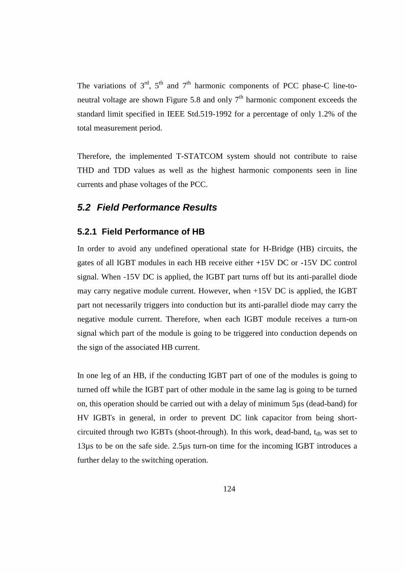
124
The variations of 3rd
, 5th
and 7th
harmonic components of PCC phase-C line-to-
neutral voltage are shown Figure 5.8 and only 7th
harmonic component exceeds the
standard limit specified in IEEE Std.519-1992 for a percentage of only 1.2% of the
total measurement period.
Therefore, the implemented T-STATCOM system should not contribute to raise
THD and TDD values as well as the highest harmonic components seen in line
currents and phase voltages of the PCC.
5.2 Field Performance Results
5.2.1 Field Performance of HB
In order to avoid any undefined operational state for H-Bridge (HB) circuits, the
gates of all IGBT modules in each HB receive either +15V DC or -15V DC control
signal. When -15V DC is applied, the IGBT part turns off but its anti-parallel diode
may carry negative module current. However, when +15V DC is applied, the IGBT
part not necessarily triggers into conduction but its anti-parallel diode may carry the
negative module current. Therefore, when each IGBT module receives a turn-on
signal which part of the module is going to be triggered into conduction depends on
the sign of the associated HB current.
In one leg of an HB, if the conducting IGBT part of one of the modules is going to
turned off while the IGBT part of other module in the same lag is going to be turned
on, this operation should be carried out with a delay of minimum 5µs (dead-band) for
HV IGBTs in general, in order to prevent DC link capacitor from being short-
circuited through two IGBTs (shoot-through). In this work, dead-band, tdb was set to
13µs to be on the safe side. 2.5µs turn-on time for the incoming IGBT introduces a
further delay to the switching operation.

125
In order to illustrate the successful operation of each HB in the field, the AC voltage
waveform of HB1 in phase-A, collector-emitter voltages and collector currents of
IGBT1 and IGBT4 modules in the upper half of HB1 are recorded in the field over
one complete cycle (20ms) and given in Figure 5.9. Charging, discharging and by-
pass periods of HB1 in phase-A are also marked on Figure 5.9-a. Conduction periods
for IGBT and anti-parallel diode parts of modules -1 and -4 are marked respectively
by S1, D1, S4 and D4 on Figure 5.9-b and -c. Output voltage polarity, current
direction, CH, DCH, and BYP modes of HB1 in phase-A of the CMC which are
shown in Figure 5.9 can be matched with those of previously constructed in Figure
4.5 and Figure 4.6 in Chapter 4.
In order to make the controller a memoryless system, a simple switching strategy is
applied at level changes and swapping instants. If a level change or swapping should
occur in the positive half-cycle of the HB voltage, IGBT modules in upper half of the
HB are controlled in order to provide a short circuit path to by-pass current (BYP1
and BYP3). However, on the negative half-cycle of the HB voltage, IGBT-2 and -3
modules of the lower half of the HB will carry the bypass current (BYP2 and BYP4
modes in Fig.13). Unfortunately, this operation strategy results in unequal utilization
IGBT modules. As an example, for the sample record given in Figure 5.9, IGBT3
and -4 modules are switched more frequently than IGBT1 and -2 modules. This is
because by-pass modes from BYP1 to BYP4 are not applied consecutively as can be
understood form Figure 5.9-a since the applied switching strategy is a memoryless
one. If a more complex control software were developed and then utilized in order to
keep the previous operation states of all IGBT modules continuously in the FPGA
memory, BYP1 mode in Figure 5.9-a would be followed by BYP2 mode sequentially
under the positive half-cycle of the HB current, however for the negative half-cycle
of the HB current BYP3 and BYP4 modes would be applied sequentially.
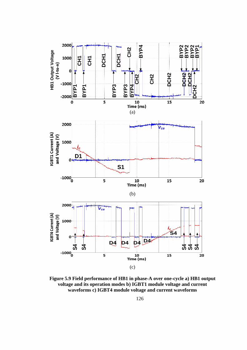
126
(a)
(b)
(c)
Figure 5.9 Field performance of HB1 in phase-A over one-cycle a) HB1 output
voltage and its operation modes b) IGBT1 module voltage and current
waveforms c) IGBT4 module voltage and current waveforms
BY
P1
BY
P1
CH
1
CH
1
DC
H1
DC
H1
BY
P3
BY
P3
CH
2B
YP
4C
H2
BY
P4
CH
2
DC
H2
BY
P2
DC
H2
BY
P2
DC
H2
BY
P2
DC
H2
BY
P1
HB
1 O
utp
ut
Vo
lta
ge
D1
S1
ic
vce
S4 D4 D4 D4 D4
S4
S4
S4
S4
S4
vce
ic
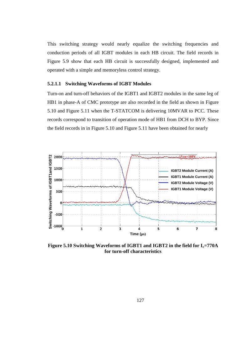
127
This switching strategy would nearly equalize the switching frequencies and
conduction periods of all IGBT modules in each HB circuit. The field records in
Figure 5.9 show that each HB circuit is successfully designed, implemented and
operated with a simple and memoryless control strategy.
5.2.1.1 Switching Waveforms of IGBT Modules
Turn-on and turn-off behaviors of the IGBT1 and IGBT2 modules in the same leg of
HB1 in phase-A of CMC prototype are also recorded in the field as shown in Figure
5.10 and Figure 5.11 when the T-STATCOM is delivering 10MVAR to PCC. These
records correspond to transition of operation mode of HB1 from DCH to BYP. Since
the field records in in Figure 5.10 and Figure 5.11 have been obtained for nearly
Figure 5.10 Switching Waveforms of IGBT1 and IGBT2 in the field for Ic=770A
for turn-off characteristics
∆Vce=160V
Time (µs)
IGBT2 Module Current (A)
IGBT1 Module Current (A)
IGBT2 Module Voltage (V)
IGBT1 Module Voltage (V)
Sw
itc
hin
g W
av
efo
rms
of
IGB
T1
an
d IG
BT
2

128
Figure 5.11 Switching Waveforms of IGBT1 and IGBT2 in the field for Ic=770A
for turn-on characteristics
rated current of Ic=770 A peak which is lower than the collector current of Ic=2175A
exercised in the laboratory switching test, a lower voltage spike of ∆Vce = 160V was
recorded (Figure 5.10). The diode reverse recovery and IGBT peak current values are
1000A and 1750, respectively as shown in Figure 5.11. The field test results of the
HB unit show that switching performances of HV IGBT modules are quite
satisfactory and consistent with design objectives.
5.2.1.2 DC Link Current and Voltage Waveforms
The variations in DC link voltage and current of HB1 in phase-A of CMC Module-1
of T-STATCOM system has been measured by an HV probe and a Rogowski coil for
a duration of 100 ms as seen in Figure 5.12 when T-STATCOM delivering -50
MVAr full capacitive to the PCC. The CMC Module-1 is under MSS method with
∆ts=400µs for the equalization of DC link capacitor voltages during the test and all
quantities are taken as 1 µs averaged data. Due to exposing high EMI/EMC
interference from the noisy environment of the test, the Rogowski coil could not
especially measure the current values at zero points accurately. The peak value of the
Sw
itc
hin
g W
av
efo
rms
of
IGB
T1
an
d IG
BT
2
Time (µs)
IGBT2 Module Current (A)
IGBT1 Module Current (A)
IGBT2 Module Voltage (V)
IGBT1 Module Voltage (V)
Irr of D2
Peak Current of IGBT1

129
DC link voltage is under 2000 V which is safe for DC link capacitors as seen from
Figure 5.12.
Figure 5.12 DC link voltage and current of HB1 in phase-A of CMC module-1
when T-STATCOM delivers -50MVAr to the PCC (1µs averaged field data)
5.2.2 Field Performance of CMC Module
5.2.2.1 Voltage Waveforms at the Input of CMC
In this subsection, line-to-line and line-to-neutral voltage waveforms at the AC input
terminals of a CMC will be given when it is producing rated MVAr in both the
inductive and capacitive regions. Figure 5.13 - Figure 5.16 show the voltage
waveforms when the CMC is operated with CSS and Modified Selective Swapping
with ∆ts=400µs. These waveforms show that the CMC successfully create 11-level
line-to-neutral and 21-level line-to-line voltage waveforms regardless of the selective
swapping technique applied.
Due to EMI/EMC Intereference of
Rogowski Coil

130
The conventional or modified selective swapping method applied to the CMC
module causes generation of voltage spikes superimposed on line-to-neutral voltage
waveforms as can be observed from Figure 5.13-b to Figure 5.16-b. These will also
reflect to the line-to-line voltage waveforms from Figure 5.13-a to Figure 5.16-a. The
cause of voltage spikes in line-to-neutral voltages is the swapping method
(conventional or modified selective swapping method) applied to the CMC module
as described in Chapter 4.1.3. During the swapping period, the conducting IGBT is
turned off and an appropriate IGBT in another HB is going to be turned on with a
delay of 13µs (deadband) in order to prevent the capacitor from being short-circuited
through two IGBTs (shoot-through) on the same leg in any HB.
Therefore in the swapping period, the current closes its path through the antiparallel
diodes of the HB whose capacitor is bypassed. This will impose +Vd or -Vd on the
line-to-neutral voltage of the associated CMC module depending upon the direction
of the current. These voltage spikes have a duration of nearly 15.5µs (13µs deadband
+ nearly 2.5µs turn-on time). Depending upon the voltage level in the line-to-neutral
voltage waveform at which the associated HBs are going to be interchanged for
swapping purpose, the magnitude of the overshoot or undershoot may be Vd, 2Vd,
3Vd or 4Vd.

131
(a)
(b)
Figure 5.13 The waveforms of a) line-to-line and b) line-to-neutral voltages for a
CMC at full inductive operation mode under Conventional Selective Swapping
(CSS) method
10 15 20 2550
Time (ms)
Line-t
o-Lin
e Volt
age (
kV)
-12
-8
-4
4
12
-16
8
0
16
20
-2030
Inductive
10 15 20 25 3050
Time (ms)
Line-t
o-Ne
utra
l Volt
age (
kV)
-8
-6
-4
0
4
-10
2
-2
6
8
10Inductive

132
(a)
(b)
Figure 5.14 The waveforms of a) line-to-line and b) line-to-neutral voltages for a
CMC at full capacitive operation mode under Conventional Selective Swapping
(CSS) method
10 15 20 2550
Time (ms)
Line-t
o-Lin
e Volt
age (
kV)
-12
-8
-4
4
12
-16
8
0
16
20
-2030
Capacitive
10 15 20 2550
Time (ms)
Line-t
o-Ne
utra
l Volt
age (
kV)
-8
-6
-4
0
4
-10
2
-2
6
8
10
30
Capacitive
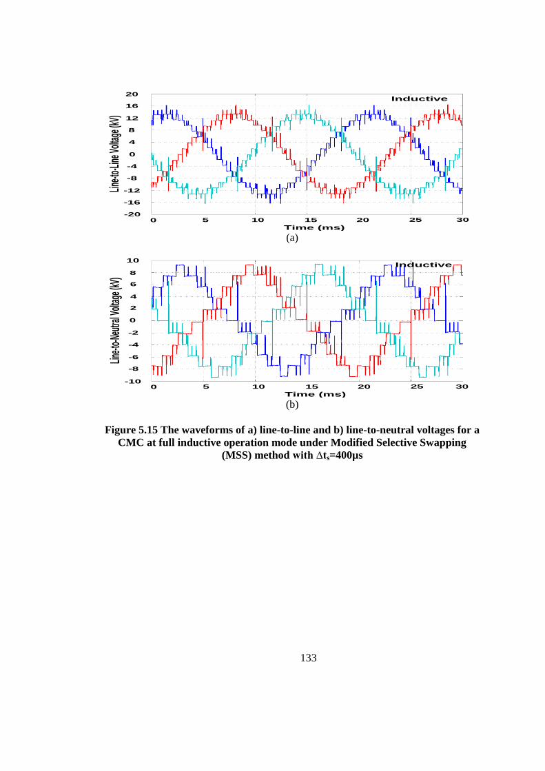
133
(a)
(b)
Figure 5.15 The waveforms of a) line-to-line and b) line-to-neutral voltages for a
CMC at full inductive operation mode under Modified Selective Swapping
(MSS) method with ∆ts=400µs
10 15 20 2550
Time (ms)
Line-t
o-Lin
e Volt
age (
kV)
-12
-8
-4
4
12
-16
8
0
16
20
-20
Inductive
30
10 15 20 25 3050
Time (ms)
Line-t
o-Ne
utra
l Volt
age (
kV)
-8
-6
-4
0
4
-10
2
-2
6
8
10Inductive

134
(a)
(b)
Figure 5.16 The waveforms of a) line-to-line and b) line-to-neutral voltages for a
CMC at full capacitive operation mode under Modified Selective Swapping
(MSS) method with ∆ts=400µs
The duration of these spikes can be reduced by choosing a smaller deadband in the
design at the expense of a lower safety factor against the risk of shoot-through.
Minimum value of the deadband is nearly 5µs. Spikes with magnitudes of ±3Vd and
±4Vd can be eliminated by optimum utilization of the switching devices at the
expense of more complex control software as described in Chapter 4.1.3. These
spikes do not reflect to the supply buses to which the T-STATCOM is connected
10 15 20 2550
Time (ms)
Line
-to-L
ine V
olta
ge (k
V)
-12
-8
-4
4
12
-16
8
0
16
20
-20
Capacitive
30
10 15 20 2550
Time (ms)
Line-t
o-Ne
utra
l Volt
age (
kV)
-8
-6
-4
0
4
-10
2
-2
6
8
10
30
Capacitive
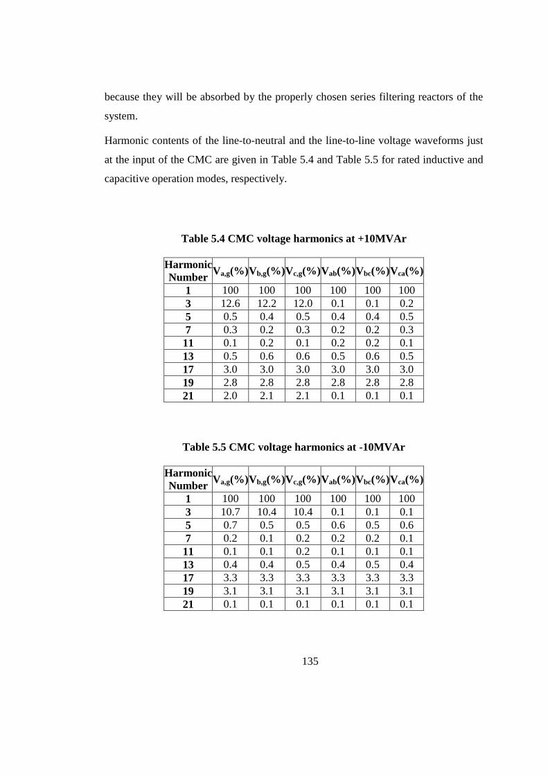
135
because they will be absorbed by the properly chosen series filtering reactors of the
system.
Harmonic contents of the line-to-neutral and the line-to-line voltage waveforms just
at the input of the CMC are given in Table 5.4 and Table 5.5 for rated inductive and
capacitive operation modes, respectively.
Table 5.4 CMC voltage harmonics at +10MVAr
Harmonic
Number Va,g(%) Vb,g(%) Vc,g(%) Vab(%) Vbc(%) Vca(%)
1 100 100 100 100 100 100
3 12.6 12.2 12.0 0.1 0.1 0.2
5 0.5 0.4 0.5 0.4 0.4 0.5
7 0.3 0.2 0.3 0.2 0.2 0.3
11 0.1 0.2 0.1 0.2 0.2 0.1
13 0.5 0.6 0.6 0.5 0.6 0.5
17 3.0 3.0 3.0 3.0 3.0 3.0
19 2.8 2.8 2.8 2.8 2.8 2.8
21 2.0 2.1 2.1 0.1 0.1 0.1
Table 5.5 CMC voltage harmonics at -10MVAr
Harmonic
Number Va,g(%) Vb,g(%) Vc,g(%) Vab(%) Vbc(%) Vca(%)
1 100 100 100 100 100 100
3 10.7 10.4 10.4 0.1 0.1 0.1
5 0.7 0.5 0.5 0.6 0.5 0.6
7 0.2 0.1 0.2 0.2 0.2 0.1
11 0.1 0.1 0.2 0.1 0.1 0.1
13 0.4 0.4 0.5 0.4 0.5 0.4
17 3.3 3.3 3.3 3.3 3.3 3.3
19 3.1 3.1 3.1 3.1 3.1 3.1
21 0.1 0.1 0.1 0.1 0.1 0.1

136
Following conclusions can be drawn from Table 5.4 and Table 5.5:
1. The SHEM applied in this research work successfully minimizes 5th
, 7th
, 11th
and 13th
harmonics in the line-to-neutral voltage waveforms.
2. Although the 3rd
harmonic component is significant in the line-to-neutral
waveforms, it becomes vanishingly small in line-to-line voltage waveforms.
5.2.2.2 Transient Performance of CMC Module
Figure 5.17 shows the the transient performance of the one of the CMC modules for
the transitifon from capacitive to inductive modes of operation.. These voltage and
current records are made at the AC input of one of the CMCs. The Qset is varied from
40 MVAr capacitive to 40 MVAr inductive. In both set of records, modulation
changes are made at zero crossing points of line current waveforms by the controller.
Figure 5.17 The transient-free transitions of CMC without feedforward
controller (CMC-side field data)
Lin
e C
urr
en
t (k
A)
Lin
e-t
o-N
eu
tra
l V
olt
ag
e (
kV
)
Time (ms)
0 20 40 60 80 100 120 140 160-10
-8
-6
-4
-2
0
2
4
6
8
10 1.0
0.8
0.6
0.4
0.2
0.0
-0.2
-0.4
-0.6
-0.8
-1.0
Ts=140ms
-40MVAr
+40MVAr

137
It is seen from Figure 5.17 that modulation index changes made at current zeros
provide a smooth transition between two operating points and no any extreme
changes in both current and voltage waveforms. A feedforward block based on the
power angle, δ against the modulation index value, M obtained by the field tests has
been applied to the closed-loop controller of DC link voltage for T-STATCOM
system. Figure 5.18 illustrates the benefits of the feedforward controller which
reduces the settling time from 140ms to 100ms.
Figure 5.18 The transient-free transitions of T-STATCOM with feedforward
controller (CMC-side field data)
Lin
e-t
o-N
eu
tra
l V
olt
ag
e (
kV
)
Lin
e C
urr
en
t (k
A)
Time (ms)
0 20 40 60 80 100 120 140 160-10
-8
-6
-4
-2
0
2
4
6
8
10 1.0
0.8
0.6
0.4
0.2
0.0
-0.2
-0.4
-0.6
-0.8
-1.0
Ts=100ms
-40MVAr
+40MVAr

138
5.2.2.3 Performance of Selective Swapping Methods on Balancing DC Link
Capacitor Voltages
The performance of MSS method in balancing the DC link voltages is investigated
by using field test results. MSS is also compared with CSS in view of the
instantaneous voltage peak-to-peak ripple, δVd, and peak-to-peak mean dc link
voltage ripple, ∆Vd, of DC link voltage and effective switching frequency, fsw(eff)
(number of turn-ons in 1 second per switch). Figure 5.19 - Figure 5.21 show the
variations in instantaneous values of DC link capacitor voltage for CSS and MSS
methods (sampling rate=1MHz). The variations in mean DC voltages (Vd,mean) are
also marked on the same waveforms (20ms averaged data).

139
(a)
(b)
Figure 5.19 Variations in the DC link voltage of an H-Bridge under
Conventional Selective Swapping (CSS) ((a) full inductive case, (b) full
capacitive case, field data)
1800
1820
1840
1860
1880
1900
1920
2000
2020
0.2 0.3 0.4 0.5 0.6 0.7 0.8 0.9 1.00.10.01760
1780
δVd
ΔVd
Vd (mean)
Time (seconds)
Cap
acit
or
Vo
ltag
e (V
olt
s)1940
1960
1980
δVd= 190 V, peak-to-peak
ΔVd= 30 V,peak-to-peak
Inductive
0.2 0.3 0.4 0.5 0.6 0.7 0.8 0.9 1.00.10.0
δVd= 205 V, peak-to-peak
ΔVd = 50 V, peak-to-peak
Vd (mean)
Time (seconds)
Cap
acit
or
Vo
ltag
e (V
olt
s)
1800
1820
1840
1860
1880
1900
1920
2000
2020
1760
1780
1940
1960
1980
δVd
ΔVd
Capacitive

140
(a)
(b)
Figure 5.20 Variations in the dc link voltage of an H-Bridge under MSS
method with ∆ts =400 μs
((a) full inductive case; (b) full capacitive case, field data)
0.2 0.3 0.4 0.5 0.6 0.7 0.8 0.9 1.00.10.0
Vd (mean)
Time (seconds)
Cap
acit
or
Vo
ltag
e (V
olt
s)
1800
1820
1840
1860
1880
1900
1920
2000
2020
1760
1780
1940
1960
1980
δVd= 145 V, peak-to-peakΔVd = 14 V,peak-to-peak
δVd
ΔVd
Inductive
0.2 0.3 0.4 0.5 0.6 0.7 0.8 0.9 1.00.10.0
δVd = 170 V, peak-to-peakΔVd = 23 V, peak-to-peak
Vd (mean)
Time (seconds)
Cap
acit
or
Vo
ltag
e (V
olt
s)
1800
1820
1840
1860
1880
1900
1920
2000
2020
1760
1780
1940
1960
1980
ΔVdδVd
Capacitive

141
(a)
(b)
Figure 5.21 Variations in the dc link voltage of an H-Bridge under MSS
method with ∆ts =200 μs
((a) full inductive case; (b) full capacitive case, field data)
These results are summarized in Table 5.6. MSS algorithm reduces considerably both
the instantaneous DC link voltage ripple and mean DC link voltage ripple at the
0.2 0.3 0.4 0.5 0.6 0.7 0.8 0.9 1.00.10.0
δVd = 130 V, peak-to-peak
ΔVd= 16 V,peak-to-peak
Vd (mean)
Time (seconds)
Cap
acit
or
Vo
ltag
e (V
olt
s)
1800
1820
1840
1860
1880
1900
1920
2000
2020
1760
1780
1940
1960
1980
δVd
ΔVd
Inductive
0.2 0.3 0.4 0.5 0.6 0.7 0.8 0.9 1.00.10.0
δVd = 190 V, peak-to-peak
ΔVd = 27 V, peak-to-peak
Vd (mean)
Time (seconds)
Cap
acit
or
Vo
ltag
e (V
olt
s)
1800
1820
1840
1860
1880
1900
1920
2000
2020
1760
1780
1940
1960
1980
δVd
ΔVd
Capacitive
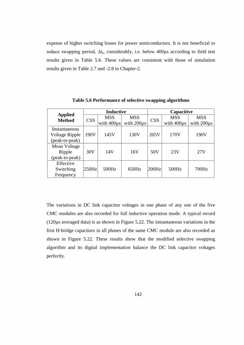
142
expense of higher switching losses for power semiconductors. It is not beneficial to
reduce swapping period, ∆ts, considerably, i.e. below 400µs according to field test
results given in Table 5.6. These values are consistent with those of simulation
results given in Table 2.7 and -2.8 in Chapter-2.
Table 5.6 Performance of selective swapping algorithms
Applied
Method
Inductive Capacitive
CSS MSS
with 400µs
MSS
with 200µs CSS
MSS
with 400µs
MSS
with 200µs
Instantaneous
Voltage Ripple
(peak-to-peak)
190V 145V 130V 205V 170V 190V
Mean Voltage
Ripple
(peak-to-peak)
30V 14V 16V 50V 23V 27V
Effective
Switching
Frequency
250Hz 500Hz 650Hz 200Hz 500Hz 700Hz
The variations in DC link capacitor voltages in one phase of any one of the five
CMC modules are also recorded for full inductive operation mode. A typical record
(120µs averaged data) is as shown in Figure 5.22. The instantaneous variations in the
first H-bridge capacitors in all phases of the same CMC module are also recorded as
shown in Figure 5.22. These results show that the modified selective swapping
algorithm and its digital implementation balance the DC link capacitor voltages
perfectly.

143
(a)
(b)
Figure 5.22 Variations in the DC link mean voltages of a CMC
((a) DC link voltages of HBs in phase-A; (b) DC link voltages of HB1s in
three phases, Field data)
Vd1,ph-A
Vd2,ph-A
Vd3,ph-A
Vd4,ph-A
Vd5,ph-A
0 0.32 0.64 0.96 1.28 1.60 1.92 2.24 2.60 2.92 3.24
Time (sec)
DC
Lin
k C
ap
ac
ito
rs M
ea
n V
olt
ag
es
(V
)
1000
1100
1200
1300
1400
1500
1600
1700
1800
1900
2000
1880
1890
1900
1910
1920
0 1.6 3.2Time (ms)
0 0.32 0.64 0.96 1.28 1.60 1.92 2.24 2.60 2.92 3.24
Time (sec)
DC
Lin
k C
ap
ac
ito
rs M
ea
n V
olt
ag
es
(V
)
1000
1100
1200
1300
1400
1500
1600
1700
1800
1900
2000
1880
1890
1900
1910
1920
0 1.6 3.2Time (ms)
Vd1,ph-A
Vd1,ph-B
Vd1,ph-C
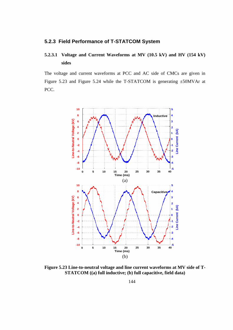
144
5.2.3 Field Performance of T-STATCOM System
5.2.3.1 Voltage and Current Waveforms at MV (10.5 kV) and HV (154 kV)
sides
The voltage and current waveforms at PCC and AC side of CMCs are given in
Figure 5.23 and Figure 5.24 while the T-STATCOM is generating ±50MVAr at
PCC.
(a)
(b)
Figure 5.23 Line-to-neutral voltage and line current waveforms at MV side of T-
STATCOM ((a) full inductive; (b) full capacitive, field data)
10 15 20 2550
Time (ms)
-6
-4
4
0
8
10
-8
Inductive
30 35 40
Lin
e C
urr
en
t (
kA
)
-3
-1
2
0
4
5
-5
2
-2
3
1
-2
-4
6
-10
Lin
e-t
o-N
eu
tra
l V
olt
ag
e (
kV
)
10 15 20 2550
Time (ms)
-6
-4
4
0
8
10
-8
Capacitive
30 35 40
Lin
e C
urr
en
t (
kA
)
-3
-1
2
0
4
5
-5
2
-2
3
1
-2
-4
6
-10
Lin
e-t
o-N
eu
tra
l V
olt
ag
e (
kV
)

145
(a)
(b)
Figure 5.24 Line-to-neutral voltage and line current waveforms at HV side of T-
STATCOM ((a) full inductive; (b) full capacitive, field data)
These waveforms have shown the success of digital implementation of the control
system as well as the Q and P control, waveform synthesizing, SHEM, Selective
Swapping and PLL techniques employed in the design and implementation of the
overall system.
10 15 20 2550
Time (ms)
Lin
e-t
o-N
eu
tra
l V
olt
ag
e (
kV
)
-100
-50
50
0
100
150
-150
Inductive
30 35 40
Lin
e C
urr
en
t (
A)
-200
-100
100
0
200
300
-300
10 15 20 2550
Time (ms)
-100
-50
50
0
100
150
-150
Capacitive
30 35 40
Lin
e C
urr
en
t (
A)
-200
-100
100
0
200
300
-300
Lin
e-t
o-N
eu
tra
l V
olt
ag
e (
kV
)

146
5.2.3.2 Voltage and Current Harmonics at PCC (154 kV)
Harmonic contents of the line-to-ground voltages at PCC with and without T-
STATCOM are as given in Table 5.7. These values are deduced from the
measurements of resistive-capacitive voltage transducers (RCVT by TRENCH). The
RCVT has a frequency bandwidth of 1MHz and can measure low order harmonic
components with unity gain. It is seen from Table 5.7 that the operation of T-
STATCOM at its rated capacity in both capacitive and inductive operation modes
does not affect the harmonic content of the PCC voltage.
Table 5.7 PCC line-to-ground voltage harmonicsmeasured by RCVT sensors
Harmonic
Number
STATCOM
Disconnected
Capacitive
Mode
Inductive
Mode IEEE
Std.519-1992
(%) Vb,g
(%)
Vc,g
(%)
Vb,g
(%)
Vc,g
(%)
Vb,g
(%)
Vc,g
(%)
1 100 100 100 100 100 100 100
3 0.6 0.5 0.6 0.5 0.6 0.5 1.0
5 0.5 0.4 0.5 0.4 0.4 0.2 1.0
7 0.4 0.3 0.4 0.3 0.3 0.2 1.0
11 0.1 0.1 0.1 0.1 0.1 0.1 1.0
13 0.1 0.1 0.1 0.1 0.1 0.1 1.0
17 0.1 0.1 0.1 0.1 0.1 0.1 1.0
19 0.1 0.1 0.1 0.1 0.1 0.1 1.0
21 0.1 0.1 0.1 0.1 0.1 0.1 1.0
THD 0.9 0.9 0.9 1.5
Harmonic contents of the coupling transformer line current waveforms on the HV
side (154 kV) are as given in Table 5.8. Both individual voltage and current
harmonic values, and THD and TDD values comply with IEEE Std. 519-1992. The
obtained field values are consistent with the desing values given in Chapter 3.

147
Table 5.8 154kV side current harmonics at rated power (IL=188A, ISC=20kA)
Harmonic
Number
Capacitive Mode Inductive Mode IEEE
Std.519-1992
(%) Ia
(%)
Ib
(%)
Ic
(%)
Ia
(%)
Ib
(%)
Ic
(%)
1 100 100 100 100 100 100 100
3 0.2 0.2 0.2 0.2 0.2 0.2 3.0
5 0.4 0.4 0.4 0.4 0.4 0.4 3.0
7 0.2 0.2 0.2 0.2 0.2 0.2 3.0
11 0.1 0.1 0.1 0.1 0.1 0.1 3.0
13 0.1 0.1 0.1 0.1 0.1 0.1 1.5
17 0.5 0.5 0.5 0.5 0.5 0.5 1.15
19 0.3 0.3 0.3 0.3 0.3 0.3 1.15
21 0.1 0.1 0.1 0.1 0.1 0.1 1.15
TDD 0.77 0.77 3.75
5.2.3.3 Effects of Series Reactors on Voltage Harmonics
Harmonic contents of the line-to-ground and line-to-line voltage waveforms on the
medium voltage side of the coupling transformer (after series connected input filter
reactor) are as given in Table 5.9.
Table 5.9 10.5kV side voltage harmonics measured by RCVT sensors
Harmonic
Number
Capacitive Mode Inductive Mode
Va,g(%) Vb,g(%) Vc,g(%) Va,g(%) Vb,g(%) Vc,g(%)
1 100 100 100 100 100 100
3 0.3 0.2 0.2 0.3 0.1 0.2
5 0.2 0.1 0.1 0.4 0.3 0.5
7 0.1 0.1 0.2 0.1 0.1 0.1
11 0.1 0.1 0.2 0.1 0.1 0.1
13 0.1 0.1 0.1 0.1 0.1 0.1
17 2.0 2.0 2.1 1.7 1.7 1.7
19 2.3 2.2 2.2 2.0 1.9 1.9
21 0.1 0.1 0.1 0.1 0.1 0.1
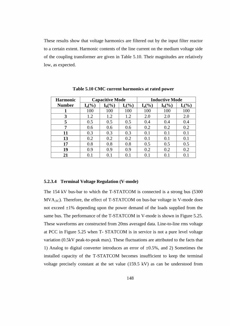
148
These results show that voltage harmonics are filtered out by the input filter reactor
to a certain extent. Harmonic contents of the line current on the medium voltage side
of the coupling transformer are given in Table 5.10. Their magnitudes are relatively
low, as expected.
Table 5.10 CMC current harmonics at rated power
Harmonic
Number
Capacitive Mode Inductive Mode
Ia(%) Ib(%) Ic(%) Ia(%) Ib(%) Ic(%)
1 100 100 100 100 100 100
3 1.2 1.2 1.2 2.0 2.0 2.0
5 0.5 0.5 0.5 0.4 0.4 0.4
7 0.6 0.6 0.6 0.2 0.2 0.2
11 0.3 0.3 0.3 0.1 0.1 0.1
13 0.2 0.2 0.2 0.1 0.1 0.1
17 0.8 0.8 0.8 0.5 0.5 0.5
19 0.9 0.9 0.9 0.2 0.2 0.2
21 0.1 0.1 0.1 0.1 0.1 0.1
5.2.3.4 Terminal Voltage Regulation (V-mode)
The 154 kV bus-bar to which the T-STATCOM is connected is a strong bus (5300
MVA,SC). Therefore, the effect of T-STATCOM on bus-bar voltage in V-mode does
not exceed ±1% depending upon the power demand of the loads supplied from the
same bus. The performance of the T-STATCOM in V-mode is shown in Figure 5.25.
These waveforms are constructed from 20ms averaged data. Line-to-line rms voltage
at PCC in Figure 5.25 when T- STATCOM is in service is not a pure level voltage
variation (0.5kV peak-to-peak max). These fluctuations are attributed to the facts that
1) Analog to digital converter introduces an error of ±0.5%, and 2) Sometimes the
installed capacity of the T-STATCOM becomes insufficient to keep the terminal
voltage precisely constant at the set value (159.5 kV) as can be understood from
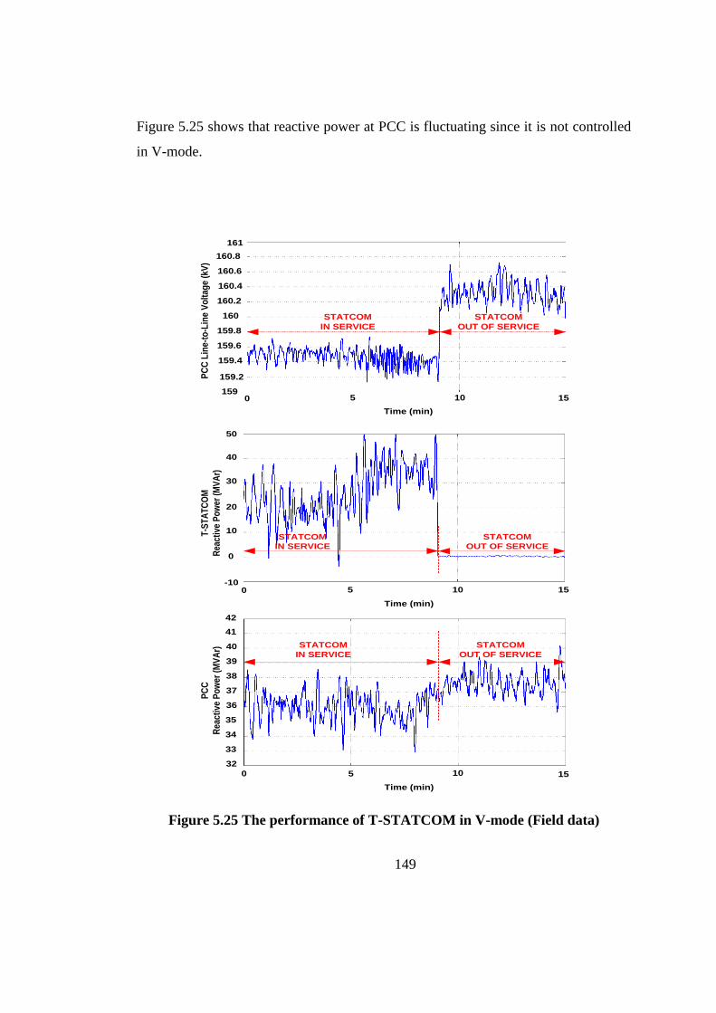
149
Figure 5.25 shows that reactive power at PCC is fluctuating since it is not controlled
in V-mode.
Figure 5.25 The performance of T-STATCOM in V-mode (Field data)
PC
C L
ine
-to
-Lin
e V
olt
ag
e (
kV
)
Time (min)
0 5159
159.2
159.4
159.6
159.8
160
160.2
160.4
160.6
160.8
10
161
STATCOM
IN SERVICE
STATCOM
OUT OF SERVICE
15
T-S
TA
TC
OM
Rea
ctiv
e P
ow
er (
MV
Ar)
-10
0
10
20
30
40
STATCOM
IN SERVICE
STATCOM
OUT OF SERVICE
50
Time (min)
0 5 10 15
PC
C
Rea
ctiv
e P
ow
er (
MV
Ar)
15
STATCOM
IN SERVICE
STATCOM
OUT OF SERVICE
Time (min)
0 105
32
33
34
35
36
37
38
39
40
41
42

150
5.2.3.5 Reactive Power Compensation (Q-mode)
The records in Figure 5.26 (20ms averaged data) show the performance of the T-
STATCOM in Q-mode. In the first 5-minute part of the record, the T-STATCOM
brings the power factor to unity as viewed from the 154 kV side of the
autotransformers. For this purpose, T-STATCOM produces nearly 45 MVAr-
inductive. When T-STATCOM is operated in standby mode to produce 0 MVAr,
nearly 27 MVAr-capacitive reactive power starts to flow to PCC via the
autotransformers. This reactive power flow is not equal to the 45 MVAr inductive
reactive power previously generated by T-STATCOM. This is attributed to the fact
that the bus voltage at PCC increases nearly 2 kV, owing to the non-linear
characteristics of power plants and loads connected to the same bus when T-
STATCOM is operating in standby mode.

151
Figure 5.26 The performance of T-STATCOM in Q-mode (Field data)
PC
C L
ine
-to
-Lin
e V
olt
ag
e (
kV
)
Time (min)
0 1 2 3 4 6158.5
159
159.5
160
160.5
161
161.5
162
162.5
163
5
163.5
STATCOM
IN SERVICESTATCOM
OUT OF SERVICE
7 8 9 10
Time (min)
0 1 2 3 4 65 7 8 9 10
T-S
TA
TC
OM
Rea
ctiv
e P
ow
er (
MV
Ar)
0
50
40
30
20
10
STATCOM
IN SERVICE
STATCOM
OUT OF SERVICE
0 1 2 3 4 65 7 8 9
PC
C
Rea
ctiv
e P
ow
er (
MV
Ar)
-40
10
0
-10
-20
-30
STATCOM
IN SERVICE
STATCOM
OUT OF SERVICE
Time (min)

152
5.2.3.6 Transitions Between Full Capacitive and Full Inductive Modes
The reactive power variations on the 10.5 kV side and 154 kV side of the coupling
transformer are given when Qset of T-STATCOM is varied from +50 MVAR
(inductive) to -50 MVAr (capacitive) in Figure 5.27-a and Figure 5.27-b,
respectively. There is a 10 MVAr (inductive) difference between the reactive power
values of 154 kV and 10.5 kV sides which is the reactive power consumption of the
coupling transformer.
(a)
(b)
Figure 5.27 Transition from a) from full inductive to full capacitive (10.5 kV
side, field data) b) full capacitive to full inductive
(154 kV side, field data)
0.0
Time (sec)
Re
ac
tiv
e P
ow
er
(MV
Ar)
0.5 1.0 1.5 2.0 2.5-60-50-40-30-20-100
10203040
-50MVAr
+50MVAr
Time (ms)20 100
-60
0
40
Ts=80ms
0.0
Time (sec)
Re
ac
tiv
e P
ow
er
(MV
Ar)
0.5 1.0 1.5 2.0 2.5-50-40-30-20-100
1020304050
Time (ms)20 120
-50
0
50
Ts=100ms
-50MVAr
+50MVAr

153
As can be seen from these waveforms in Figure 5.27-a, the settling time of the closed
loop control system is only 80ms. On the other hand, when Qset is varied from -50
MVAr (capacitive) to +50 MVAr (inductive), the response of the closed loop control
system will be as in Figure 5.27-b. For this case, the settling time is measured to be
100ms. It is worth to note that if the T-STATCOM were operated in open loop
control mode, the settling time would not exceed 45ms.
The line-to-neutral voltage waveform and the associated line current waveform on
the 10.5 kV side of the coupling transformer during transition from Qset = +50 MVAr
to -50 MVAr with the closed loop control system are given in Figure 5.28. The
associated waveforms from Qset= -50 MVAr to +50 MVAR are shown in Figure
5.29. The responses in Figure 5.28 and Figure 5.29 show the smooth and fast
response of the control system against changes in Qset from full inductive to full
capacitive, or vice versa.
Figure 5.28 Variations in line-to-ground voltage and current during the
transition from full inductive to full capacitive (10.5 kV side, field data)
10 10
Lin
e-t
o-N
eu
tra
l V
olt
ag
e (
kV
)
Lin
e C
urr
en
t (k
A)
Time (ms)
0 20 40 60 80 100 120 140 160-10
-8
-6
-4
-2
0
2
4
6
8 8
6
4
2
0
-2
-4
-6
-8
-10
Ts=80ms
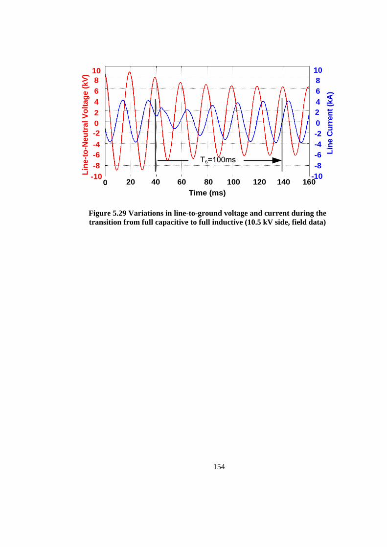
154
Figure 5.29 Variations in line-to-ground voltage and current during the
transition from full capacitive to full inductive (10.5 kV side, field data)
Lin
e-t
o-N
eu
tra
l V
olt
ag
e (
kV
)
Lin
e C
urr
en
t (k
A)
Time (ms)
0 20 40 60 80 100 120 140 160-10
-8
-6
-4
-2
0
2
4
6
8
10 10
8
6
4
2
0
-2
-4
-6
-8
-10
Ts=100ms
155
CHAPTER 6
CONCLUSIONS
Nowadays, FACTS are being increasingly used in power systems, to enhance the
system utilization and power transfer capacity as well as the stability, security,
reliability and power quality of AC system interconnections. Among FACTS
devices, the shunt controllers have shown feasibility in terms of in a wide range of
problem-solving abilities from transmission to distribution levels. For decades, it has
been realized that by manipulating the compensated reactive power, the transmittable
active power through the interconnected networks can be increased without installing
new transmission lines and the voltage profile of the buses can also be controlled
easily by the shunt controllers.
As a shunt controller, Static Synchronous Compensator (STATCOM) systems are
being installed for transmission and distribution levels. They are based on switching
power converters employing turn-off capable semiconductor switches and hence they
may operate under high switching frequency and provide faster response. Two-level,
six-pulse bridge converters with relatively high switching frequencies and relatively
low installed capacities are usually being the characteristics of Distribution type
STATCOM (D-STATCOM) systems. These are usually connected to the Medium
Voltage (MV) load bus via a step-up coupling transformer. However, Transmission
type STATCOM (T-STATCOM) systems have much higher installed capacities and
therefore the power semiconductors in their converter system/s should be switched at
156
lower frequencies. That is why in practical applications of T-STATCOM systems
either multi-pulse converters or Multilevel Converter (MC)s are to be utilized. These
systems are connected to the High Voltage (HV) or extra high voltage (EHV) buses
of the transmission systems via coupling transformers.
Among the mature multilevel converter topologies, due to its modularity, flexibility
and less number of power components, Cascaded Multilevel Converter (CMC)
topology is the most promising alternative for T-STATCOM applications. It is
possible to reach high voltage levels by the use of appropriate number of HBs
connected in series for CMC topology. By it modular structure, the CMC can
flexibly expand the output power capability if needed and is favorable to
manufacturing. Moreover, redundancy can be easily applied in the CMC to enhance
reliability for the entire system.
This research and technology development work deals with the sizing, system and
power-stage designs of an HV IGBT based CMC for T-STATCOM applications.
System design and the number of H-Bridge (HB)s in each phase of the Y-connected
CMC are achieved in view of Total Harmonic Distortion (THD) at Point of Common
Coupling (PCC), Total Demand Distortion (TDD) of the line currents and individual
harmonic current limits recommended by IEEE Std.519-1992. A 12 kV, ±10 MVAr,
11-level CMC Module power stage with five HBs in each phase is designed and then
implemented to deliver ±10MVAr to 154kV transmission bus (PCC) via a series
filter reactor and 154/10.5kV coupling transformer. Therefore, the CMC module
presented in this work constitutes a building block of large T-STATCOM systems.
The Selective Harmonic Elimination Method (SHEM) is applied to synthesize T-
STATCOM voltage waveforms at power frequency (50Hz) and the Modified
Selective Swapping (MSS) Algorithm is exercised to balance the DC link capacitor
voltages, perfectly at the expense of higher switching frequency, and hence switching
losses. The power stage is carefully designed and its performance is optimized in
view of the current HV IGBT technology.

157
A 154kV, ±50 MVAr, 11-level T-STATCOM system by the parallel use of five
CMCs built in this work has been implemented in the field primarily for the purposes
of reactive power compensation and terminal voltage regulation, and secondarily for
power system stability. Since the operating voltage of CMC is chosen to be 10.5 kV
(max.12 kV) line-to-line, it is connected to 154 kV line-to-line transmission bus
through a specially designed 50/62.5 MVA Y-Y connected (YNyn vector group)
coupling transformer and each CMC module is connected to secondary side of the
coupling transformer via a series filter reactor bank. This is the first industry
application of wire-bond HV IGBT based CMC in T-STATCOM applications. Five
±12 MVAr, 10.5 kV CMC modules are operated in parallel by the specially designed
fully digital control system composed of DSP and FPGAs.
In the thesis, it is found that the number of HBs in series for CMC topology is not the
only parameter on complying with THD and TDD limits specified in IEEE 519-
1992. The series filter inductance value has also a great effect on THD and TDD
limits. Therefore, choosing Lr value for CMC topology is a crucial issue when
designing the system. As the value of series filter inductance rises, the THD and
TDD values decrease for CMC topologies with three, five and seven HBs while the
variations in AC input voltage of the CMC from full inductive operation to full
capacitive operation becomes significantly high. Moreover, there is an optimum
point of DC link voltage and M-range value for each CMC topology in view of
complying with THD and TDD limits.
A Modified Selective Swapping (MSS) algorithm has been applied by the control
system to reduce the instantaneous DC link voltage ripple of H-Bridges by an
amount of 33%, and the mean DC link voltage ripple by an amount of 50%, as
compared to the Conventional Selective Swapping (CSS) algorithm, thus resulting in
perfect balancing of the H-bridge DC link voltages at the expense of higher
semiconductor switching losses. The variations in instantaneous peak-to-peak and
mean voltages decrease with MSS methods with low values of ∆ts while the effective
158
switching frequency of power semiconductors increases. Therefore, for practical
applications, a compromise should be made between the instantaneous peak-to-peak
voltage and the effective switching frequency. Beyond a ∆ts value such as
∆ts=1000µs, no difference exists between CSS and MSS methods for variations in
DC link instantaneous peak-to-peak voltages.
In this work, the switching strategy chosen in the application of both CSS and MSS
causes voltage spikes with magnitudes ±Vd, ±2Vd, ±3Vd and ±4Vd superimposed
on the 11-level line-to-neutral voltage waveform. However, the voltage spikes
arising from the application of MSS and CSS methods and superimposed on 11-level
line-to-neutral voltage waveforms do not lead to an operational problem for the T-
STATCOM and power system because they are successfully suppressed by the total
series reactance as can be observed from line-to-neutral voltage waveforms at 154kV
PCC. Also, the utilizations of the HV IGBTs used in each HB are not equal due to
the use of a simple memoryless control system. However, the switching strategies to
eliminate or decrease the duration of the superimposed voltage spikes and to equlize
the utilizations of the HV IGBTs are shown to be possible in this work by using more
complex control systems.
Moreover, a compromise is made between the turn-on and turn-off behaviors of the
HV IGBTs. This is achieved by the followings:
a. Using laminated bus technology, Lstray is reduced to 75nH for each HB;
b. By modifying the standard IGBT driver circuit, turn-on time is prolonged to 2.5µs;
c.Using DC link capacitors with very low equivalent series inductances
(Lself=50nH//50nH) and directly mounting them on the laminated bus to minimize
the wiring inductance. For the purpose of the decreasing the Irr and hence peak turn-
on currents of the HV IGBT modules, the modification is made on the gate drive
circuits by increasing the turn-on control resistance, Rg(on) from 2.0 Ω to 3.2 Ω.
After modifying gate driver circuit, the turn-on time is found to be 2.5µs for HV
IGBT modules. This reduces the reverse recovery current of anti-parallel diodes from
159
1500A to 1250A and hence decreases the peak turn-on current of IGBT2 from
2500A to 2250 A for the worst case in the transient state of the CMC operation.
Therefore, after modification, the diode and IGBT parts of HV IGBT modules can be
safely operated since their current and voltage magnitudes remain inside the related
SOAs. However, after this modification, the reverse recovery loss, Err of the diode
part decreases by a percentage of 10.11% and the turn-on loss, Eon of the IGBT part
increases by a percentage of 17.30%.
Furthermore, owing to the application of the Selective Harmonic Elimination Method
(SHEM), the 5th
, 7th
, 11th
, and 13th
voltage harmonics are successfully minimized. It
has been shown by field tests that the total harmonic distortion (THD) of the line-to-
neutral voltage waveform at the point of common coupling is as small as 0.9% with
respect to the fundamental component. The total demand distortion (TDD) has been
measured as 0.77%, in the 154 kV bus.
The transient response of the developed system is also found to be quite satisfactory.
The settling time of the T-STATCOM at full-load from inductive mode to capacitive
mode transition, and vice versa have been recorded as 80ms and 100ms, respectively
in the field, with a transient free transition between modes. The modularity of H-
Bridges for easy replacement in the case of a failure, and the mobility and flexibility
of the overall T-STATCOM for easy relocation when necessary are being further
advantages of the developed system.
Based on these operating principles described in this work, not only qualitative
but also quantative design criteria for developing a CMC based T-STATCOM have
been given. These are summarized in Table 6.1.
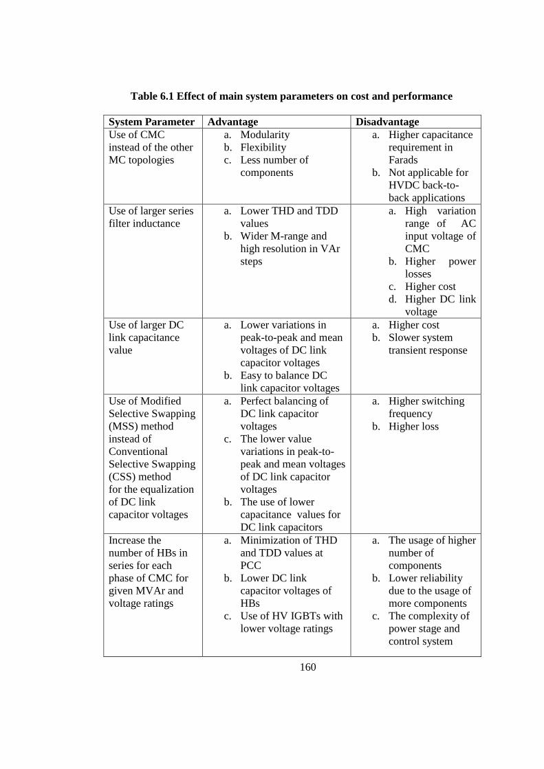
160
Table 6.1 Effect of main system parameters on cost and performance
System Parameter Advantage Disadvantage
Use of CMC
instead of the other
MC topologies
a. Modularity
b. Flexibility
c. Less number of
components
a. Higher capacitance
requirement in
Farads
b. Not applicable for
HVDC back-to-
back applications
Use of larger series
filter inductance
a. Lower THD and TDD
values
b. Wider M-range and
high resolution in VAr
steps
a. High variation
range of AC
input voltage of
CMC
b. Higher power
losses
c. Higher cost
d. Higher DC link
voltage
Use of larger DC
link capacitance
value
a. Lower variations in
peak-to-peak and mean
voltages of DC link
capacitor voltages
b. Easy to balance DC
link capacitor voltages
a. Higher cost
b. Slower system
transient response
Use of Modified
Selective Swapping
(MSS) method
instead of
Conventional
Selective Swapping
(CSS) method
for the equalization
of DC link
capacitor voltages
a. Perfect balancing of
DC link capacitor
voltages
c. The lower value
variations in peak-to-
peak and mean voltages
of DC link capacitor
voltages
b. The use of lower
capacitance values for
DC link capacitors
a. Higher switching
frequency
b. Higher loss
Increase the
number of HBs in
series for each
phase of CMC for
given MVAr and
voltage ratings
a. Minimization of THD
and TDD values at
PCC
b. Lower DC link
capacitor voltages of
HBs
c. Use of HV IGBTs with
lower voltage ratings
a. The usage of higher
number of
components
b. Lower reliability
due to the usage of
more components
c. The complexity of
power stage and
control system
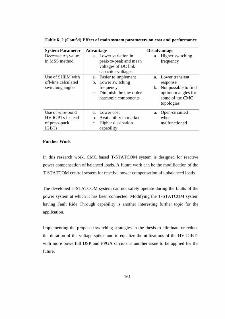
161
Table 6. 2 (Cont’d) Effect of main system parameters on cost and performance
System Parameter Advantage Disadvantage
Decrease ∆ts value
in MSS method
a. Lower variation in
peak-to-peak and mean
voltages of DC link
capacitor voltages
a. Higher switching
frequency
Use of SHEM with
off-line calculated
switching angles
a. Easier to implement
b. Lower switching
frequency
c. Diminish the low order
harmonic components
a. Lower transient
response
b. Not possible to find
optimum angles for
some of the CMC
topologies
Use of wire-bond
HV IGBTs instead
of press-pack
IGBTs
a. Lower cost
b. Availability in market
c. Higher dissipation
capability
a. Open-circuited
when
malfunctioned
Further Work
In this research work, CMC based T-STATCOM system is designed for reactive
power compensation of balanced loads. A future work can be the modification of the
T-STATCOM control system for reactive power compensation of unbalanced loads.
The developed T-STATCOM system can not safely operate during the faults of the
power system at which it has been connected. Modifying the T-STATCOM system
having Fault Ride Through capability is another interesting further topic for the
application.
Implementing the proposed switching strategies in the thesis to eliminate or reduce
the duration of the voltage spikes and to equalize the utilizations of the HV IGBTs
with more powerfull DSP and FPGA circuits is another issue to be applied for the
future.

162
REFERENCES
[1] “Proposed terms and definitions for flexible AC transmission system
(FACTS),” IEEE Trans. Power Delivery, vol. 12, no. 4, Oct. 1997, pp.
1848–1853.
[2] C.O. Gerçek, M. Ermis, A. Ertas, K.N. Kose, O. nsar, “Design,
Implementation, and Operation of a New C-Type 2nd Harmonic Filter for
Electric Arc and Ladle Furnaces”, IEEE Trans. Ind. Appl., vol.47,
pp.1545-1557, July/Aug.2011.
[3] N. G. Hingorani and L. Gyugyi, “Understanding FACTS: concepts and
technology of flexible AC transmission systems,” IEEE Press, 2000.
[4] H. F. Bilgin, M. Ermis, K. N. Kose, A. Cetin, I. Cadirci, A. Acik, T.
Demirci, A. Terciyanli, C. Kocak, M. Yorukoglu, “Reactive-Power
Compensation of Coal Mining Excavators by Using a New-Generation
STATCOM”, IEEE Trans. Ind. Appl., vol. 43, o. 1, pp. 97 – 110,
Jan/Feb.2007.
[5] Y. Sumi,Y. Harumoto, T. Hasegawa, M. Yano, K. Ikeda, T. Matsuura,
“New Static VAr Control Using Force-Commutated Inverters”, IEEE
Power Eng.Review, vol. PER-1, no. 9 , pp. 33 – 34, Sep.1981.
[6] S. Mori, K. Matsuno, T. Hasegawa, S. Ohnishi, M. Takeda, M. Seto, S.
Murakami, F. Ishiguro, “Development of a large static VAr generator
using self-commutated inverters for improving power system stability”,
IEEE Trans. Power Systems, vol. 8 ,pp. 371 – 377, Feb.1993.

163
[7] C. Schauder, M. Gernhardt, E. Stacey, T. Lemak, L. Gyugyi, T.W. Cease,
A. Edris, “Development of a ±100 MVAr static condenser for voltage
control of transmission systems”, IEEE Trans. Power Delivery, vol. 10 ,
no. 3 , pp. 1486 – 1496, July1995.
[8] G.F. Reed, J.E. Greaf, T. Matsumoto, Y. Yonehata, M. Takeda, T.
Aritsuka, Y. Hamasaki, F. Ojima, A.P. Sidell, R.E. Chervus, C.K.
Nebecker, “Application of a 5 MVA, 4.16 kV D-STATCOM system for
voltage flicker compensation at Seattle Iron and Metals”, IEEE Power
Eng. Society Summer Meeting 2000, vol. 3, pp. 1605 – 1611.
[9] L. Wenhua, L. Xu, L. Feng, L. Chenglian, G. Hang, “Development of 20
MVA static synchronous compensator”, IEEE Power Eng. Society Winter
Meeting 2000, vol. 4, pp. 2648 – 2653.
[10] G. Reed, J. Paserba, T. Croasdaile, M. Takeda, N. Morishima, Y.
Hamasaki, L. Thomas, W. Allard, “STATCOM application at VELCO
Essex substation”, IEEE/PES Trans. Dist. Conf. Exhibition 2001, vol. 2,
pp. 1133 – 1138.
[11] G. Reed, J. Paserba, T. Croasdaile, R. Westover, S. Jochi, N. Morishima,
M. Takeda, T. Sugiyama, Y. Hamasaki, T. Snow, A. Abed, “SDG&E
Talega STATCOM project-system analysis, design, and configuration”,
IEEE/PES Trans. Dist. Conf. Exhibition 2002: Asia Pacific, vol. 2, pp.
1393 – 1398.
[12] D.J. Hanson, C. Horwill, B.D. Gemmell, D.R. Monkhouse, “A
STATCOM-based relocatable SVC project in the UK for National Grid”,
IEEE Power Eng. Society Winter Meeting 2002, vol. 1, pp. 532 – 537.
[13] R. Grunbaum, T. Gustafsson, J.-P. Hasler, T. Larsson, M. Lahtinen,
“STATCOM, a prerequisite for a melt shop expansion-performance
experiences”, IEEE Power Tech Conf. Proceedings 2003, vol.2., 2003.
[14] J. Sun, L. Hopkins, B. Shperling, B. Fardanesh, M. Graham, M. Parisi,
S.MacDonald, S.Bhattacharya, S.Berkowitz, A.Edris, “Operating
164
characteristics of the convertible static compensator on the 345 kV
network”, IEEE PES Power Systems Conf. Expo. 2004, vol.2, pp. 732 –
738.
[15] K. Fujii, K. Kunomura, K. Yoshida, A. Suzuki, S. Konishi, M. Daiguji,
K. Baba, “STATCOM applying flat-packaged IGBTs connected in
series”, IEEE Trans. Power Electron., vol. 20, pp. 1125 – 1132,
Sep.2005.
[16] A. Oskoui, B. Mathew, J.-P. Hasler, M. Oliveira, T. Larsson, A.
Petersson, E. John, “Holly STATCOM - FACTS to Replace Critical
Generation, Operational Experience”, IEEE/PES Trans. Dist. Conf.
Exhibition, 2005/2006, pp. 1393 – 1398.
[17] K. Hidese, T. Ishizuka, F. Aoyama, S. Ota, K. Ogushi, “Development on
31.5MVA STATCOM and digital evaluation tool for voltage flicker
compensation”, 7th Int. Conf. on Power Electronics 2007, pp.1230 –
1234.
[18] T. Fujii, K. Temma, N. Morishima, T. Akedani, T. Shimonosono, H.
Harada, “450 MVA GCT- STATCOM for stability improvement and
over-voltage suppression”, 2010 Int. Power Electronics Conf., pp. 1766 –
1772, 2010.
[19] R. Gr nbaum, T. Gustafsson, J. Hasler, M. Osada, J. Rasmussen, K.
Thorburn, “STATCOM for flicker suppression from a steel plant
connected to a weak 66 kV grid”, 2010 Int. Power Electronics Conf., pp.
1773 – 177, 2010.
[20] M. Pereira, D. Retzmann, J. Lottes, M. Wiesinger, G. Wong, “SVC
PLUS: An MMC STATCOM for network and grid access applications”,
IEEE PowerTech, 2011 Trondheim, pp.1 – 5, 2011.
[21] B. Gultekin, C.O. Gercek, T. Atalik, M. Deniz, N. Bicer, M. Ermis, K.N.
Kose, C. Ermis, E. Koc, I. Cadirci, A. Acik, Y. Akkaya, H. Toygar, S.
Bideci, “Design and Implementation of a 154-kV, ±50-Mvar

165
Transmission STATCOM Based on 21-Level Cascaded Multilevel
Converter”, IEEE Trans. Ind. Appl., vol. 48 , no. 3, pp. 1030 – 1045,
May/June 2012.
[22] T. Atalik, M. Deniz, E. Koc, C.O. Gercek, B. Gultekin, M. Ermis, I.
Cadirci,” Multi-DSP and -FPGA-Based Fully Digital Control System for
Cascaded Multilevel Converters Used in FACTS Applications”, IEEE
Trans. Ind. Info., vol. 8 , no. 3, pp. 511 – 527, 2012.
[23] H.F. Bilgin, M. Ermis, “Design and Implementation of a Current-Source
Converter for Use in Industry Applications of D-STATCOM”, IEEE
Trans. Power Electron. , vol. 25 , no. 8 , pp. 1943 – 1957, Aug.2010.
[24] H.F. Bilgin, M. Ermis, “Current source converter based STATCOM:
Operating principles, design and field performance”, Elsevier Electric
Power Systems Research, vol.81, no.2, pp. 478-487, Feb.2011
[25] A. Cetin, M. Ermis, “VSC-Based D-STATCOM With Selective
Harmonic Elimination”, IEEE Trans. Ind. Appl., vol. 45, no. 3, pp 1000 –
1015,May/June 2009.
[26] A. Cetin, H.F. Bilgin, A. Acik, T. Demirci, K.N. Kose, A. Terciyanli, B.
Gultekin, N. Aksoy, B. Mutluer, I. Cadirci, M. Ermis, K. Ongan, N.
Akinci, “Reactive Power Compensation of Coal Conveyor Belt Drives by
Using D-STATCOMs” , IEEE Ind. Appl. Conf., 42nd IAS Annual
Meeting Conference Record of the 2007, pp. 1731 – 1740.
[27] M. Malinowski, K. Gopakumar, J. Rodriguez, M.A. P re , “A Survey on
Cascaded Multilevel Inverters”, IEEE Trans. Ind. Electron., vol. 57, no.
7, pp. 2197 – 220, July 2010.
[28] H. Abu-Rub, J. Holtz, J. Rodriguez, G. Baoming, “Medium-Voltage
Multilevel Converters—State of the Art, Challenges, and Requirements in
Industrial Applications”, IEEE Trans. Ind. Electron., vol. 57, no. 8, pp.
2581 - 2596, Aug.2010.

166
[29] J. Rodriguez, J.-S. Lai, F.Z. Peng, “Multilevel inverters: a survey of
topologies, controls, and applications”, IEEE Trans. Ind. Electron., vol.
49, no. 4, pp. 724 – 738, Aug.2002.
[30] H. Akagi, “Large static converters for industry and utility applications”,
Proceedings of the IEEE 2001, vol. 89, no. 6, pp. 976 – 983, 2011.
[31] H. Akagi, “Classification, Terminology, and Application of the Modular
Multilevel Cascade Converter (MMCC)”, IEEE Trans. Power Electron.,
vol.26, no. 11, pp. 3119 – 3130, Nov. 2011.
[32] P. Rodriguez, M.D. Bellar, R.S. Munoz-Aguilar, S. Busquets-Monge, F.
Blaabjerg, “Multilevel-Clamped Multilevel Converters (MLC 2)”, IEEE
Trans. Power Electron., vol. 27, no. 3, pp. 1055 – 1060, March 2012.
[33] L.A. Tolbert, F. Z. Peng; T. Cunnyngham, J.N. Chiasson, “Charge
balance control schemes for cascaded multilevel converter in hybrid
electric vehicles”, IEEE Trans. Ind. Electron., vol. 49, no. 5, pp.1058 -
1064, Oct.2002.
[34] J.A. Barrena, L.Marroyo, M.A.R. Vidal, J.R.T. Aprai , “Individual
Voltage Balancing Strategy for PWM Cascaded H-Bridge Converter-
Based STATCOM”, IEEE Trans. Ind. Electron., vol. 55, no. 1, pp.21 -
29, Jan.2008.
[35] Y. Liu, A.Q. Huang, W. Song, S. Bhattacharya, G. Tan, “Small-Signal
Model-Based Control Strategy for Balancing Individual DC Capacitor
Voltages in Cascade Multilevel Inverter-Based STATCOM”, IEEE
Trans. Ind. Electron., vol. 56 , no. 6 , pp. 2259 – 2269, June2009.
[36] S. Vazquez, J.I. Leon, J.M. Carrasco, L.G. Franquelo, E. Galvan, M.
Reyes, J.A. Sanchez, E. Domingue , “Analysis of the Power Balance in
the Cells of a Multilevel Cascaded H-Bridge Converter”, IEEE Trans.
Ind. Electron., vol. 57, no. 7, pp.2287 – 2296, July2010.
167
[37] Z. Liu, B. Liu, S. Duan, Y. Kang, “A Novel DC Capacitor Voltage
Balance Control Method for Cascade Multilevel STATCOM”, IEEE
Trans. Power Electron., vol. 27, pp.14 – 27, Jan.2012.
[38] J. Napoles, A. Watson, J. Padilla, J. Leon, L. Franquelo, W. Patrick, M.
Agirre, “Selective Harmonic Mitigation Technique for Cascaded H-
Bridge Converters with Non-Equal DC Link Voltages”, IEEE Trans. Ind.
Electron., Early Access Articles, 2012.
[39] S. Du, J. Liu, J. Lin, Y. He, “A Novel DC Voltage control method for
STATCOM based on Hybrid Multilevel H-bridge Converter”, IEEE
Trans. Power Electron., Early Access Articles, 2012.
[40] H. Sepahvand, J. Liao, M. Ferdowsi, K. Cor ine, “Capacitor Voltage
Regulation in Single-DC-Source Cascaded H-bridge Multilevel
Converters Using Phase-Shift Modulation”, IEEE Trans. Ind. Electron.,
Early Access Articles, 2012.
[41] K. Ilves, A. Antonopoulos, S. Norrga, H.- P. Nee, “A New Modulation
Method for the Modular Multilevel Converter Allowing Fundamental
Switching Frequency”, IEEE Trans. Power Electron., vol. 27, no. 8 ,
pp.3482 – 3494, Aug.2012.
[42] M. Hagiwara, R. Maeda, H. Akagi, “Control and Analysis of the Modular
Multilevel Cascade Converter Based on Double-Star Chopper-Cells
(MMCC-DSCC)”, IEEE Trans. Power Electron., vol. 26, no. 6, pp.1649
– 1658, June2011.
[43] M. Hagiwara, H. Akagi, “Control and Experiment of Pulse width-
Modulated Modular Multilevel Converters”, IEEE Trans. Power
Electron., vol. 24, no. 7, pp.1737 – 1746, July2009.
[44] H. Akagi, S. Inoue, T. Yoshii, “Control and Performance of a
Transformerless Cascade PWM STATCOM With Star Configuration”,
IEEE Trans. Ind. Appl., vol. 43, no. 4, pp.1041 – 1049, Aug.2007.
168
[45] J. -S. Lai, F. Z. Peng, “Multilevel Converters-A New Breed of Power
Converters,” IEEE Trans. Ind. App., vol. 32, no. 3, pp. 509–517,
May/June 1996.
[46] F. Z. Peng, J. W. McKeever, D. J. Adams, “Cascade Multilevel Inverters
for Utility Applications,” in 1997 Proc. IECON Conf., vol. 2, pp. 437–
442.
[47] F. Z. Peng, J. -S. Lai, J. W. McKeever, J. VanCoevering, “A Multilevel
Voltage-Source Inverter with Separate DC Sources for Static Var
Converters,” IEEE Trans. Ind. App., vol. 32, no. 5, pp. 1130–1138,
Sep./Oct. 1996.
[48] L. M. Tolbert, J. N. Chiasson, F. Z. Peng, “Modulation Index Regulation
of a Multilevel Inverter for Static Var Compensation,” in Conf. Rec. 2003
IEEE Power Eng. Society General Meeting, vol. 1, pp. 194–199, 2003.
[49] S. Sirisukprasert, J. -S. Lai, A. Q. Huang, “Modeling, Analysis and
Control of Cascaded Multilevel Converter Based STATCOM,” in Conf.
Rec. 2003 IEEE Power Eng. Society General Meeting, vol. 4, pp. 2561–
2568,2013.
[50] S. Sirisukprasert, “Modeling and Control of a Cascaded-Multilevel
Converter-Based STATCOM,” Ph.D. dissertation, Dept. Elect. and
Comp. Eng., Virginia Tech. Univ., Blacksburg, VA, Feb. 2004.
[51] L. M. Tolbert, F. Z. Peng, T. G. Habetler, “Multilevel Converters for
Large Electric Drives,” IEEE Trans. Ind. App., vol. 35, no. 1, pp. 36–44,
Jan./Feb. 1999.
[52] B. Ozpineci, L. M. Tolbert, J. N. Chiasson, “ Harmonic Optimi ation of
Multilevel Converters Using Genetic Algorithms,” IEEE Power
Electronics Letters, vol. 3, no. 3, pp. 92–95, Sep. 2005.
[53] Recommended Practices and Requirements for Harmonic Control in
Electrical Power Systems, IEEE Std.519, 1992.
[54] IEC Standard Voltages, IEC 60038, Edition 6-2, 2002-07.
169
[55] A. Cetin, “Design and Implementation of a voltage source converter
based STATCOM for reactive power compensation and harmonic
filtering”, Ph.D. dissertation, Dept. Elect. and Electron. Eng., METU.,
April 2007.
[56] Electromagnetic Compatibility (EMC)-Part 4-30: Testing and
Measurement Techniques-Power quality measurement method, IEC
61000-4-30

170
APPENDIX-A
SHEM EQUATIONS FOR 11-LEVEL CMC
The line-to-neutral waveform for 11-level CMC shown in Figure 2.7 of Chapter-2 can
be expressed by:
(A1.1)
Since the output voltage is odd-quarter wave;
(A1.2)
and
(A1.3)
Assuming DC link capacitor voltages are all balanced and equal to Vd;
(A1.4)
The fundamental component is below as shown in (A1.5).
(A1.5)
To eliminate low order harmonics of 5th, 7th, 11th and 13th in the phase-to-neutral
voltages of CMC by the switching angles of θ1, θ2,...., θ5, the following equations are to
be used:
(A1.6)

171
(A1.7)
(A1.8)
(A1.9)
(A1.10)

172
APPENDIX-B
PERMISSIBLE REGIONS FOR THD AND TDD
RECOMMENDED BY IEEE STD.519-1992
Figure B.1 Permissible regions for total harmonic distortion (THD) and total
demand distortion (TDD) as a function of rated voltage at point of common
coupling (PCC) as recommended by IEEE Std.519, 1992.
TD
D (
%)
PCC Voltage (kV)
69 1610
5.0
2.5
1.5
20.00
10.00
5.00
2.503.75
∫∫
Permissible Regions as
recommended by IEEE Std.519,1992
THD at PCC
TDD for strong supply
TDD for weak supply
TH
D (
%)
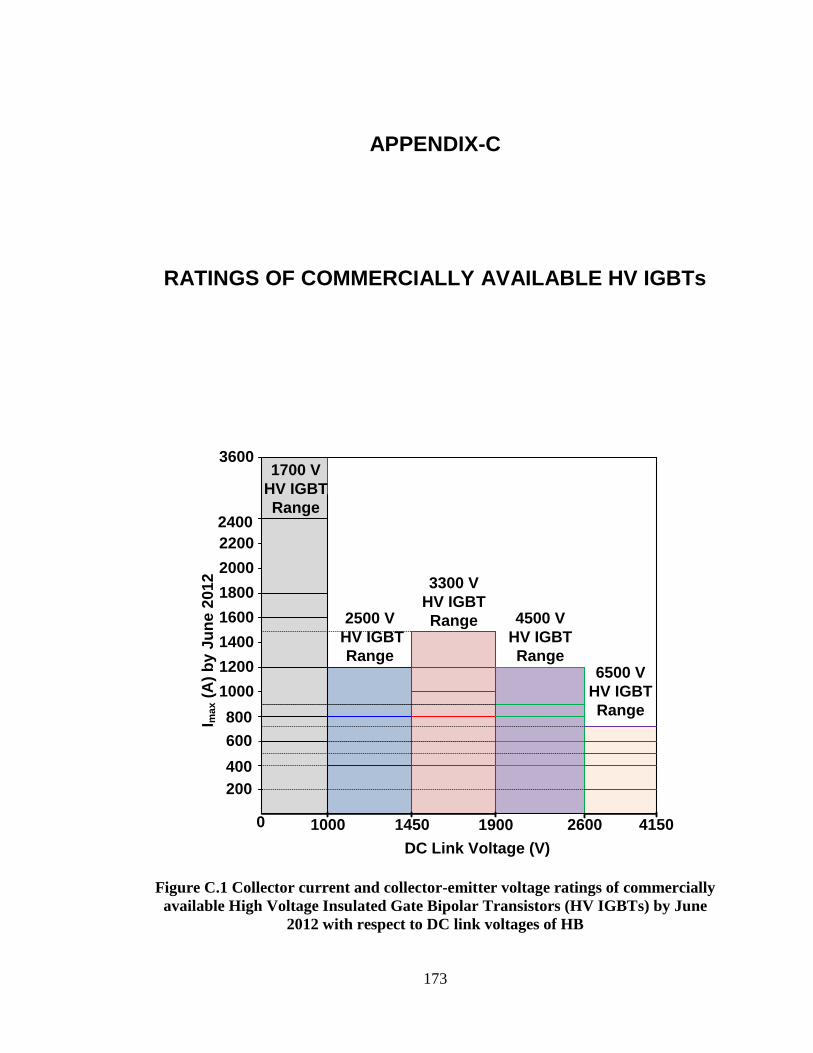
173
APPENDIX-C
RATINGS OF COMMERCIALLY AVAILABLE HV IGBTs
Figure C.1 Collector current and collector-emitter voltage ratings of commercially
available High Voltage Insulated Gate Bipolar Transistors (HV IGBTs) by June
2012 with respect to DC link voltages of HB
I ma
x (
A)
by
Ju
ne
20
12
DC Link Voltage (V)
1450 26000
400
800
1200
1600
2000
2400
1000 1900 4150
1700 V
HV IGBT
Range
2500 V
HV IGBT
Range
3300 V
HV IGBT
Range 4500 V
HV IGBT
Range6500 V
HV IGBT
Range
200
600
1000
1400
1800
2200
3600

174
APPENDIX-D
SOAs OF MITSUBISHI CM1200HC-66H HV IGBT
MODULE
Figure D.1 Safe Operating Areas (SOA) of HV IGBT modules specified in
datasheet of MITSUBISHI CM1200HC-66H

175
CURRICULUM VITAE
PERSONAL INFORMATION
Surname, Name: Gültekin, Burhan
Nationality: Turkish (TC)
Date and Place of Birth: 11 November 1979-IĞDIR
Marital Status: Married
Phone: +90 312 2101310
Fax: +90 312 2101315
email: [email protected]
EDUCATION
Degree Institution Year of Graduation
MS METU Electrical and Electronics Eng. 2003
BS METU Electrical and Electronics Eng. 2000
WORK EXPERIENCE
Year Place Enrollment
2006 - Present TUBITAK UZAY Chief Senior Researcher
2003 - 2006 TUBITAK UZAY Senior Researcher
2000 - 2003 TUBITAK UZAY Researcher
FOREIGN LANGUAGES
English

176
PUBLICATIONS
1. B. Gultekin, C.O. Gercek, etal, “Design and Implementation of a 154-kV, ±50-Mvar
Transmission STATCOM Based on 21-Level Cascaded Multilevel Converter”, IEEE
Trans. Ind. Appl., vol. 48 , no. 3, pp. 1030 – 1045, May/June 2012.
2. T. Atalik, M. Deniz, E. Koc, C.O. Gercek, B. Gultekin, M. Ermis, I. Cadirci,
“Multi-DSP and -FPGA-Based Fully Digital Control System for Cascaded
Multilevel Converters Used in FACTS Applications”, IEEE Trans. Ind. Info.,
vol. 8 , no. 3, pp. 511 – 527, 2012.
3. M. Ermis, A. Acik, B. Gultekin, etal “Power quality solutions for 12-pulse smelter
converters in ETI aluminum works”, IEEE Trans.Ind.Apps., vol.40, no.6, pp.1644-1655,
2004.
4. O. Salor, B. Gultekin,etal “Electrical Power Quality of Iron and Steel Industry in
Turkey”, IEEE Trans.Ind.Apps., vol.46, no.1, pp.60-80, 2010
5. B. Mutluer, I. Cadirci, M. Ermis, A. Cetin, N. Ozay, B. Gultekin, etal “A unified
relocatable SVC for open-cast lignite mining in Turkey”, IEEE Trans.Ind.Apps., vol.40,
no.2, pp.650-663, 2004.
6. N. Kose, B. Mutluer, M. Ermis, A. Terciyanlı, Gultekin B.,etal “Two-folded
implementation of a 12-pulse TCR with dissimilar transformers for a ladle
furnace: reactive power compensation and power system redundancy”, IEEE
Industrial Applications Annual Conference, Oct. 2004.
7. A. Terciyanli, M. Ermis, B. Gultekin, O.B. Tor, M. Yorukoglu “EMC
considerations in the design of a unified relocatable SVC for open-cast lignite
mining in Turkey”, IEEE International Symposium on Electromagnetic
Compatibility, vol.2, pp.991-994, 2003.
8. Cetin, A.; Bilgin, H.F.; Acik, A.; Demirci, T.; Kose, K.N.; Terciyanli, A.;
Gultekin, B. etal “Reactive Power Compensation of Coal Conveyor Belt Drives
by Using D-STATCOMs”, IEEE Industry Applications Conference, pp.1731-
1740, 2007.
9. M. Deniz, B. Gultekin, C.O. Gercek, T. Atalik, I. Cadirci, M. Ermis “A new DC
voltage balancing method for cascaded multilevel inverter based STATCOM”,

177
International Aegean Conference on Electrical Machines and Power Electronics,
pp.532-535, 2007.