chapter 2 multilevel inverters -...
TRANSCRIPT
15
CHAPTER 2
MULTILEVEL INVERTERS
2.1 INTRODUCTION
Switched mode inverters find wide applications in power industry. These
inverters require control of both the magnitude and frequency of an ac output.
Practically, inverters are used in both single phase and three phase AC systems.
A half bridge inverter is the simplest topology, which is used to produce a two level
square wave output waveform. A center tapped voltage source supply is needed in
such a topology. On the other hand, the full bridge topology is used to synthesize
both three level and two level output waveforms [45].
However, the above mentioned inverters have limitations in handling
high voltage and high power conversion. For higher output voltage capacity and
reduction in harmonic distortion, these converters need to be connected in series
using transformers. Also, these series connection of inverters are the contributors to
problems such as bulkiness, high loss and high cost to the overall AC system.
Besides that, conventional inverters have some disadvantages operating at high
frequency mainly due to switching losses and constraints of the device ratings.
To overcome the disadvantages of conventional inverters, multilevel
inverters emerge as the new breed of converters in high and medium power
applications. A multilevel converter not only achieves high power ratings, but also
enables the use of renewable energy sources. Renewable energy sources such as
photovoltaic, wind and fuel cells can be easily interfaced to a multilevel converter
system for a high power application [94].

16
The elementary concept of a multilevel inverter to achieve high power is
to use a series of power semiconductor switches with several lower voltage dc
sources to perform the power conversion by synthesizing a staircase voltage
waveform. The input dc voltages can be derived from fuel cells, capacitors or
renewable energy voltage sources.
This chapter reviews state of the art of multilevel inverter technology.
Fundamental multilevel inverter structures are discussed including the pros and cons
of each technique.
Multilevel inverter topologies are classified into three types:
1. Diode clamped multilevel inverter,
2. Flying capacitor multilevel inverter and
3. Cascaded H-bridge multilevel inverter.
2.2 DIODE CLAMPED MULTILEVEL INVERTER (DC MLI)
Nabae et al (1981) proposed a neutral point inverter called three level
diode clamped inverter. The diode clamped inverter uses a single dc bus that is
subdivided into a number of voltage levels by a series string of capacitors. A matrix
of semiconductor switches and diodes allows each phase leg to be switched to any of
these voltage levels [14].
A m-level diode clamped inverter requires
� Number of dc bus capacitors (Ndc) = (m-1)
� Number of clamping diodes (Ncd) = (m-1)(m-2)
� Number of semiconductor swithces(Nss) = 2(m-1)
� For a five level inverter m = 5.
Figure 2.1 shows a three phase five level diode clamped inverter. It
consists of four capacitors C1, C2, C3 and C4. For a dc bus voltage Vdc, voltage across

17
each capacitor is Vdc / 4 and voltage stress across each device is limited to one
capacitor voltage.
The staircase output phase voltage is synthesized, by considering the
negative dc rail 0 as the reference point. Following five switch combinations
synthesize five level voltages across a and 0.
(1) For voltage level Va0 = Vdc, turn on all upper switches Sa1 through
Sa4.
(2) For voltage level Va0 = 3Vdc/4, turn on three upper switches Sa2
through Sa4 and one lower switch S’a1.
(3) For voltage level Va0 = 2Vdc/4, turn on two upper switches Sa3 and
Sa4 and two lower switches S’a1 and S’a2
(4) For voltage level Va0 = Vdc/4, turn on one upper switch Sa4 and
three lower switches S’a1 through S’a3
(5) For voltage level Va0 = 0, turn on all lower half switches S’a1
through S’a4
Figure 2.1 Three phase diode clamped multilevel inverter

18
Table 2.1 gives the switching sequence for obtaining the required output
voltage in a diode clamped multilevel inverter.
Table 2.1 Switching sequence for diode clamped five level inverter
Output Voltage Va0
Switching StatesSa1 Sa2 Sa3 Sa4 S’a1 S’a2 S’a3 S’a4
Vdc 1 1 1 1 0 0 0 03Vdc/4 0 1 1 1 1 0 0 02Vdc/4 0 0 1 1 1 1 0 0Vdc/4 0 0 0 1 1 1 1 0Vdc=0 0 0 0 0 1 1 1 1
A m-level inverter has a m-level output phase voltage and a (2m-l) level
output line voltage.
2.2.1 Features of Diode Clamped Multilevel Inverter
High voltage rating for blocking diodes
Although each switching device is only required to block a voltage level
of Vdc / (m-l), the clamping diodes need to have different voltage ratings for reverse
voltage blocking. In Figure 2.1, when all lower switches S’a1 through S’a4 are turned
on, Da1 needs to block three capacitor voltages or 3Vdc /4. Similarly, Da2 and D’a2
need to block 2 Vdc /4 and Da3 needs to block Vdc /4. If the blocking voltage rating of
each diode is the same as that of the switching device, the number of diodes required
for each phase will be (m-l) x (m-2). This number represents a quadratic increase in
ma. When ma is sufficiently high, the number of diodes required will make the
system impractical to implement which in turn limits the number of levels.
Unequal device rating
From Table 2.1, it can be seen that switch Sa1 conducts only during
Va0 = Vdc, while switch Sa4 conducts over the entire cycle except Vao= 0. Such an
unequal conduction duty requires different current ratings for switching devices.

19
When the inverter design is to use the average duty for all devices, the upper
switches may be oversized and the lower switches may be undersized. If the design
is to suit the worst case, then there will be 2 x (m-2) upper devices oversized.
Capacitor voltage unbalance
In most applications, a power converter needs to transfer real power from
ac to dc (rectifier) or dc to ac (inverter operation). When operating at unity power
factor, the charging time (or discharging time for inverter operation) for each
capacitor is different. The charging profile of such a capacitor repeats every half
cycle and the result is unbalanced capacitor voltages between different levels. This
voltage unbalance problem in a multilevel inverter can be solved by several
approaches, such as replacing capacitors by a controlled constant dc voltage source,
pulse width modulation, voltage regulators or batteries.
Advantages
� When the number of levels is high enough, harmonic content will
be low enough to avoid the need for filters.
� Efficiency is high because all the devices are switched at the
fundamental frequency.
� Reactive power flow can be controlled.
� The control method is simple for a back-to-back inertia system.
Disadvantages
� Excessive clamping diodes are required when the number of levels
is high.
� It is difficult to control the real power flow for the individual
converter.
2.3 FLYING CAPACITOR MULTILEVEL INVERTER (FC MLI)
Meynard and Foch introduced flying capacitor based inverter in 1992.
This inverter uses capacitors to limit the voltage of the power devices. The structure

20
of this inverter is similar to that of diode clamp type inverter except that capacitors
are used to divide the input voltage [14, 63].
An m-level flying capacitor inverter requires
� Number of dc bus capacitors (Ndc) = (m-1)
� Total number of balancing capacitors (Nbc) = (m-1)(m-2) /2
� Number of semiconductor switches (Nss) = 2(m-1)
Figure 2.2 shows the structure of a three phase full bridge flying
capacitor based five level inverter. Each phase leg has an identical structure.
Assuming that each capacitor has the same voltage rating, the series connection of
capacitors in Figure 2.2 is to indicate the voltage level between the clamping points.
Three inner loop balancing capacitors for phase leg A (Ca1, Ca2, Ca3) are independent
of those for phase leg B. All phase legs share the same dc link capacitors, C1 through
C4.
Figure 2.2 Three phase flying capacitor multilevel inverter

21
The voltage synthesis in a flying capacitor inverter has more flexibility
than a diode clamped inverter. The phase voltage of Va0 of a m-level inverter has m
levels and the line voltage has (2m-1) levels. An output with respect to the negative
dc rail Va0 can be synthesized by the following switching combinations:
For an output voltage level Vao = Vdc, turn on all upper switches Sa1 through Sa4
For an output voltage level Va0 = 3Vdc / 4, there are four combinations:
a. Va0 = Vdc-Vdc/4 by turning on devices Sa1, Sa2, Sa3, S’a4
b. Va0 = 3Vdc/4 by turning on devices Sa2, Sa3, Sa4, S’a1
c. Va0 = Vdc- 3Vdc/4 + Vdc/2 by turning on devices Sa2, Sa3, Sa4, and S’a1
d. Va0 = Vdc- 2Vdc/4 + Vdc/4 by turning on devices Sa1, Sa2, Sa4 and S’a3
For an output level Va0 = 2Vdc / 4, there are six combinations:
a. Va0 = Vdc-Vdc/2 by turning on devices Sa1, Sa2, S’a3 and S’a4
b. Va0 = 2Vdc/4 by turning on devices Sa3, Sa4, S’a1 and S’a2
c. Va0 = Vdc-3Vdc/4+Vdc/2-Vdc/4 by turning on devices Sa1, Sa3, S’a2 and
S’a4
d. Va0 = Vdc-3Vdc/4 +Vdc/4 by turning on devices Sa1, Sa4, S’a2 and S’a3
e. Va0 = 3Vdc/4-Vdc/2 +Vdc/4 by turning on devices Sa2, Sa4, S’a1and S’a3
f. Va0 = 3Vdc/4 -Vdc/4 by turning on devices Sa2, Sa3, S’a1 and S’a4
For an output level Va0 =Vdc / 4, there are four combinations:
a. Va0 = Vdc-3Vdc/4 by turning on devices Sa1, S’a2, S’a3 and S’a4
b. Va0 = Vdc/4 by turning on devices Sa4, S’a1, S’a2 and S’a3
c. Va0 = Vdc/2-Vdc/4 by turning on devices Sa3, S’a1, S’a2 and S’a4
d. Va0 = 3Vdc/4-Vdc/2 by turning on devices Sa2, S’a1, S’a3 and S’a4
For an output level Va0 = 0, turn on all lower half switches S’a1 through S’a4.

22
Table 2.2 Switching sequence for flying capacitor five level inverter
Output Voltage
Va0
Switching StatesSa1 Sa2 Sa3 Sa4 S’a1 S’a2 S’a3 S’a4
Vdc 1 1 1 1 0 0 0 0
3Vdc/4 1 1 1 0 1 0 0 0
2Vdc/4 1 1 0 0 1 1 0 0
Vdc/4 1 0 0 0 1 1 1 0
Vdc=0 0 0 0 0 1 1 1 1
Table 2.2 lists the possible switching combinations of flying capacitor
multilevel inverter. The state condition one represents the switch is ON and zero
represents the switch is OFF.
2.3.1 Features of Flying Capacitor Multilevel Inverter
Large number of capacitors
The inverter requires a large number of storage capacitors. If the voltage
rating of each capacitor used is the same as that of the main power switch, a
m-level inverter requires a total of (m-l) x (m-2) / 2 auxiliary capacitors per phase
leg in addition to (m-1) main dc bus capacitors, whereas a m-level diode clamped
inverter requires only (m-1) capacitors of same voltage rating.
Balancing capacitor voltages
For producing the same output voltage, the inverter can involve different
combinations of capacitors allowing preferential charging and discharging of
individual capacitors. This flexibility makes it easier to manipulate the capacitor
voltages and keep them at their proper values. In order to balance the capacitor
charging and discharging, one may employ two or more switch combinations for
middle voltage levels (i.e., 3Vdc/4, Vdc/2 and Vdc/4) in one or several fundamental
cycles. Thus, by proper selection of switching combinations, the flying capacitor
23
multilevel inverter may be used in real power conversions. However, when it
involves real power conversions, the selection of a switch combination becomes
very complicated and the switching frequency needs to be higher than the
fundamental frequency.
Advantages
� Large amount of storage capacitors can provide ride through
capabilities during power outage.
� These inverters provide switch combination redundancy for
balancing different voltage levels.
� Like DC MLI, the harmonic content is low enough to avoid the
need for filters.
� Both real and reactive power flow can be controlled.
Disadvantages
� Excessive number of storage capacitors is required when the
number of levels is high. High level systems are more difficult to
package and more expensive with the required bulky capacitors.
� The inverter control is very complicated and the switching
frequency and switching losses are high for real power transmission.
2.4 CASCADED H-BRIDGE MULTILEVEL INVERTER (CHB MLI)
Cascaded multilevel inverters are based on a series connection of several
single phase inverters. As each inverter can be seen as a module with similar circuit
topology, control structure and modulation, these converters feature a high
modularity degree. Therefore, in the case of a fault in one of these modules, it is
possible to replace it quickly and easily. Moreover, with an appropriate control
strategy, it is possible to bypass the faulty module without stopping the load,
bringing an almost continuous overall availability [14, 63].

24
A m-level cascaded H-bridge inverter requires:
� Number of separate dc sources (Ndcs) = (m-1) / 2
� Number of semiconductor switches (Nss) = 2(m-1)
The multilevel inverter synthesizes desired output voltage from several
separate DC sources. DC sources can be of batteries, fuel cells or solar cells. Each
inverter can produce three output voltage levels, namely, +Vdc, −Vdc and 0 by
connecting the dc source to the output side by different switching combinations of
four switches. As shown in equation (2.1), the phase output voltage is synthesized
by the sum of each individual inverter output voltage.
( ) ( ) ( ) ( ) ( )tV+......+tV+tV+tV=tV oN3o2o1oo (2.1)
where N is the number of cascaded bridges. The output voltage is almost sinusoidal.
By controlling the conducting angles at different levels, harmonic distortion of the
output voltage can be minimized.
Figure 2.3 Three phase cascaded H-bridge multilevel inverter

25
If all dc voltage sources are equal to Vdc, the inverter is then known as a
symmetrical multilevel inverter and all the power semiconductors will be capable of
blocking the same voltage in their ‘off’ state. The effective number of output voltage
levels m in symmetric multilevel inverter related to the cell number is given by
equation (2.2)
N2+1=m (2.2)
where m is the number of levels generated. In multilevel inverter with two dc
sources, the maximum output voltage VoMax can be determined by equation (2.3).
dcoMax NV=V (2.3)
As shown in Figure 2.3, a three-phase five level cascaded H-bridge
inverter requires two H-bridge cells with eight switches per phase. Thus a total of
six H-bridge cells involving twenty four power switches are required for this circuit
configuration. This means that twelve pairs of gating signals have to be generated to
be fed to the switches. Each switch operates only at fundamental frequency. By
increasing the number of cells, the converter can naturally reach higher voltages
with the same power semiconductors. This modularity is especially useful for high
power applications (several kilovolts and megawatts).
Table 2.3 lists the possible switching combinations of cascaded H-bridge
multilevel inverter. The state condition one represents the switch is ON and zero
represents the switch is OFF.
Table 2.3 Switching sequence for cascaded H-bridge five level inverter
Output Voltage Va0
Switching StatesSA1 SA2’ SA2 SA1’ SA3 SA4’ SA4 SA3’
Vdc 1 1 0 0 0 0 0 02Vdc 1 1 0 0 1 1 0 0Vdc 0 0 0 0 1 1 0 00 0 0 0 0 0 0 0 0
-Vdc 0 0 1 1 0 0 0 0-2Vdc 0 0 1 1 0 0 1 1-Vdc 0 0 0 0 0 0 1 1
26
2.4.1 Features of Cascaded H-bridge Multilevel Inverter
� For real power conversions, (ac to dc and dc to ac), the cascaded inverter needs separate dc sources. The structure of separate dc sources is well suited for various renewable energy sources such as
fuel cell, photovoltaic and bio-mass etc.
� Connecting separate dc sources between two converters in a back-
to-back fashion is not possible because a short circuit will be introduced when two back-to-back converters are not switching synchronously [14, 63].
Advantages
� CHB MLI requires least number of components among all multilevel converters to achieve the same number of voltage levels.
� Modularized circuit layout and packaging is possible because each level has the same structure and there are no extra clamping diodes or voltage balancing capacitors.
� Soft switching can be used in this structure to avoid bulky and loss producing resistor-capacitor-diode snubbers.
Disadvantages
� CHB MLI needs separate dc sources for real power conversions, and thus its applications are somewhat limited.
2.5 PULSE WIDTH MODULATION TECHNIQUES
Pulse width modulation methods are the one which are used for adjusting
the ON and OFF periods of inverter switches. In earlier days, conventional two level inverters were controlled by fundamental switching frequency. Since, it has some
limitations like high switching losses and constraints of power device ratings, high total harmonic distortion etc, the multilevel inverters operating at high switching frequencies arrived which solve the above mentioned shortcomings to some extent.
27
This chapter presents the concept of sine pulse width modulation with
single reference based on various control degrees of freedom combination. Various
parameters like total harmonic distortion, RMS voltage, DC utilization rate,
distortion factor and crest factor are determined to verify the effective performance
of the three phase CHB MLI.
Generally, PWM methods create load voltage harmonics, which are
responsible for overall system losses. To minimize the losses, the switching angle at
each instant needs to be calculated accurately. Each of these switching angles can be
evaluated by Fourier series to eliminate certain harmonics as shown in
equation (2.4) [58].
( ))tωnsin(b+)tωncos(a+2
a=S
1=nnn
0)t(angle
(2.4)
where a0 = average DC value of the switching signal.
The coefficients a0, an and bn are given below as
dtSπ1
=aπ
π-)t(angle0
(2.5)
dt)tωn(CosSπ1
=aπ
π-)t(anglen
(2.6)
dt)tωn(SinSπ1
=bπ
π-)t(anglen
(2.7)
Different PWM techniques with variation in the existence of harmonic
components are available. The choice of selecting the PWM techniques and its
output voltage requirements depend upon the applications. Among all the available
PWM techniques, SPWM technique is the most popular modulation technique for
inverter’s switch control, which has been explained in the forthcoming section of
this chapter.

28
Based on the nature of generation of modulating signals, the control
schemes for cascaded H-bridge MLI are classified as shown in Figure 2.4.
2.5.1 Selective Harmonic Elimination PWM
The Selective Harmonic Elimination PWM (SHE PWM) technique is
based on the fundamental switching frequency theory proposed by Patel in 1974 and
it is dependent on the elimination of defined harmonic content orders. A set of
transcendental equations describing the Fourier equations linked to the number of
the harmonics that can be eliminated needs to be written down. Solving this set of
trigonometric equations will yield a solution in which the output voltage will not
contain harmonics [30, 55, 61].
Figure 2.4 Types of PWM control techniques

29
As an example, the general Fourier series expansion of the five level
inverter output voltage is given as:
( ) )tωn(Sin )θn(Cos+)θn(Cos
πnV4
=)tω(V 21...5,3,1=n
dc (2.8)
where n defines the harmonic order at the output voltage of MLI. To eliminate 5th,
7th, 11th and 13th harmonics, the switching angles θ1, θ2 etc at fundamental switching
frequency can be calculated as:
a21 m2=)θ(Cos+)θ(Cos (2.9)
0=)θ5(Cos+)θ5(Cos 21 (2.10)
0=)θ7(Cos+)θ7(Cos 21 (2.11)
0=)θ11(Cos+)θ11(Cos 21 (2.12)
0=)θ13(Cos+)θ13(Cos 21 (2.13)
The switching angles are determined for minimizing the total harmonic
distortion and ma represents the amplitude modulation index. The above mentioned
non linear equations are solved by an iterative method like Newton-Raphson
method. When ma changes, the angle coefficient θ changes and can be calculated
mathematically as mentioned above.
The main disadvantage of this method is the laborious calculations
involved in determining the switching angles as in fundamental frequency switching
method. Though Newton-Raphson iteration method is used to solve the equation, it
does not provide an accurate solution as the initial values are fixed only by
assumption. In addition, the increased DC sources or switching angles will prevent
obtaining the most accurate solution [30].

30
2.5.2 Space Vector Pulse Width Modulation
The Space Vector Modulation (SVM) can be implemented with both the
high and low switching frequencies. In space vector modulation scheme, the
sampled value of reference voltage vector is realized by switching the nearest
voltage space vectors. The major advantage of utilizing the SVM scheme is the
increased utilization of DC supply, reduced total harmonic distortion etc [39-40]. In
SVM method, the switching vectors are represented via hexagon and sub triangles
within hexagon. For multilevel inverters, as the level increases, the number of sub
triangles within the hexagon increases which in turn paves the way for complexity.
Based on the synchronous frame, the possible output vector voltages of voltage
source inverter are expressed as
( ) θj240jcn
120jbnanqd eV=eV+eV+V
32
=jV+V=Vοο
(2.14)
2.5.3 Advanced Modulation Techniques
2.5.3.1 Trapezoidal Modulation
In this PWM method, the gating signals are generated by comparing the
carrier signal (triangular or inverted sine carrier wave) with the trapezoidal
waveform [63]. The angle of the flat portion of this wave is given by
���� )a1(2 (2.15)
where a = signal reference of amplitude Maximum
signal reference of Amplitude
This type of modulation increases the peak fundamental output voltage of
up to 1.05V, but the output contains lower order harmonics.

31
2.5.3.2 60 degree PWM
In 60 degree PWM, the modulating sine wave is flat topped for a period
of 60 degrees in each half cycle i.e from 60 to 120 degree and 240 to 300 degree.
This type of PWM reduces the switching losses and utilizes more of the available dc
voltage [63].
2.5.3.3 Stepped modulation
In this type of modulation, one cycle of operation is divided into
specified intervals, say 20o, 30o, etc., with each interval controlled individually to
control the magnitude of the fundamental component and to eliminate specific
harmonics. This type of control gives low distortion and higher fundamental
amplitude compared with that of normal PWM method but contains low order
harmonics [63].
2.5.3.4 Staircase modulation
In staircase modulation method, the levels are calculated to eliminate
specific harmonics. Frequency modulation index and number of steps are chosen to
obtain the desired quality of the output voltage. This is an optimized PWM and is
not recommended for fewer than 15 pulses in one cycle [63].
2.5.3.5 Delta modulation
In this modulation method, first the upper and lower limit of the
modulating wave is fixed and a triangular wave is allowed to oscillate in that band
and through this it is compared with the carrier signals for generating gate pulses.
This method is also known as hysteresis modulation. This method has the
individuality of controlling the ratio of voltage to frequency, a desirable feature for
ac motor control applications. [63]

32
2.5.3.6 Harmonic injection modulation
The summation of fundamental switching wave and selected frequency waves as a modulating wave is compared with the carrier for the elimination of specific harmonics in the output voltage. For example, if we take a triplen harmonic wave as a modulating wave for the evaluation of the system’s performance, itconsists of frequency components of fundamental, third and ninth harmonic wave and it can be represented as,
tω9Sin 029.0+tω3Sin 27.0+tωSin 15.1=Vo (2.16)
As a result of this modulation, the output voltage levels do not contain the triplen harmonics [63].
2.5.4 Sinusoidal Pulse Width Modulation Technique
In sinusoidal PWM technique, a low frequency sinusoidal control voltage is compared with a high frequency triangular carrier signal to generate the gate signals for the inverter. This technique has many advantages like low switching losses, low harmonics, better output voltage etc [30, 58].
With the help of this technique, the cascaded H-bridge five level inverter synthesizes the resulting phase voltage by the addition of the voltages generated by individual H-bridge (2 H-bridges) cells.
N0040302010 V+.........+V+V+V+V=V (2.17)
where N is the number of H-bridges. Based on the number of carriers used, SPWM methods can be classified into two types as, single carrier PWM method and multicarrier PWM method.
In single carrier PWM method, a high frequency carrier is compared with a low frequency single or dual modulating waves. The pulses that have been produced due to the intersection of carrier and modulating wave are given to the respective inverter switches. The widths of the pulses can be varied by controlling the amplitude of the modulating signal to control the output voltage. With the help

33
of this technique, the harmonic content can be reduced using several pulses in each half cycle of output voltage. This type of method is also called as uniform pulse width modulation [63]. The modulation index controls the output voltage which varies in linear modulation range and its instantaneous value is given by
)g-g(VV 41s0 � (2.18)
where Vs is the dc source voltage value, g1 and g4 are gate signals during the
operating period of the inverter [63].
In case of multicarrier PWM technique, single / dual modulating wave is
compared with more than one carrier to generate the pulses. The pulses generated
are used to control the power switches of the circuit [22, 51].
2.6 MULTICARRIER PULSE WIDTH MODULATION
In multicarrier pulse width modulation, the carriers are arranged above
and below of zero reference, based on control degrees of freedom combinations.
These carriers have constant period, therefore the switches have constant switching
frequency. The switching instants are determined at the intersecting points during
the comparison of carriers and the modulating signal [95]. For a m-level cascaded
inverter, this strategy arranges m-1 triangular carriers with the same frequency and
amplitude so that they fully occupy contiguous bands over the range +Vdc to -Vdc.
Every instant each carrier is compared with the modulating signal. Each
comparison gives +1, -1 if the modulating sinusoid is greater than / lower than the
triangular carrier in the first / second half of the fundamental period and zero
otherwise. The results are added to give the voltage level, which is required at the
output terminal of the inverter [3]. The frequency of the output voltage is determined
by the frequency of the sinusoidal reference waveform. The amplitude of the
fundamental component of the output voltage is determined by the amplitude
modulation index ma. This method is based on the comparison of sinusoidal
reference waveforms with carrier waveforms [43, 48, 62].

34
For a three phase five level inverter system, three sinusoids which are
120ο phase shifted are compared with four carriers to generate the required level [23,
36]. Generally, the carriers can be of triangular, inverted sine wave and saw tooth
wave in nature [60].
For a five level cascaded H-bridge inverter shown in Figure 2.5, the
pulses which have been generated by comparing the modulating and the carrier
waves are used to control the operation of S1, S4, S1’, S4’ in the positive half. By the
same way, in the negative half side, the generated pulses are used to trigger S2, S3,
S2’, S3’ switches of a single phase H-bridge MLI.
In this chapter, carriers arranged in bipolar mode are compared with the
single reference of a pure sine wave [27, 48, 64].
The representation of modulating signal is denoted as Vi(t), where i = a,
b, c and is given by
)t(h+)t(V=)t(V i*
ii (2.19)
where )t(hi are injected harmonics and )t(V *i are fundamental three phase
symmetrical sinusoidal signals given by equations 2.20-2.22.
Figure 2.5 Single phase cascaded H-bridge five level inverter
35
)tωsin(m=)t(V a*
a (2.20)
)3π2
+tωsin(m=)t(V a*
b (2.21)
)3π4
+tωsin(m=)t(V a*
c (2.22)
where am is the modulation index and
0=)t(V+)t(V+)t(V *c
*b
*a (2.23)
Therefore, )t(hi is usually called as zero sequence signal and can be
calculated by
( ))t(V+)t(V+)t(V31
=)t(h cbai (2.24)
and 0=)t(hi yields sinusoidal PWM [39].
Modulation index plays a vital role in deciding the ability of a PWM
method for delivering AC output voltage. The modulation index can be of amplitude
modulation index or frequency modulation index.
Frequency Modulation Index ( fm )
Frequency modulation index is defined as the ratio of carrier frequency
( cf ) to that of fundamental frequency ( mf ) and is represented as,
m
cf f
f=m
(2.25)
Amplitude Modulation Index ( am )
Amplitude modulation index is defined as the ratio of the amplitude of
modulating wave ( mA ) to that of carrier wave ( cA ) and is represented as

36
c
ma A
Am � (2.26)
In the case of amplitude modulation index, the operation of PWM can be
categorized as:
(a) Linear modulation range: In this, the ratio of the maximum
amplitude of the modulating wave to that of carrier wave is always
less than or equal to one.
(b) Non linear modulation range: This is otherwise called as over
modulation range where the amplitude of modulating signal is
always greater than that of carrier signals and its modulation index
is always greater than one [39].
With respect to the arrangement of carrier, the multicarrier PWM
techniques are classified as level shifted PWM, phase shifted PWM and hybrid
PWM method. This chapter of the thesis presents the analysis of cascaded H-bridge
five level inverter under linear modulation range.
2.6.1 Level / Vertically Shifted PWM
Level shifted technique is the logical extension of sine triangle PWM for
multilevel inverters, in which m-1 carriers are needed for m-level (five level)
inverter. They are arranged in vertical shifts in continuous bands defined by the
levels of the inverter [57]. 3(m-1) carriers are required for three phases.
Based on control degrees of freedom combinations, the level shifted
PWM is divided into phase disposition, alternate phase opposition disposition and
phase opposition disposition [22, 27, 51, 62].
37
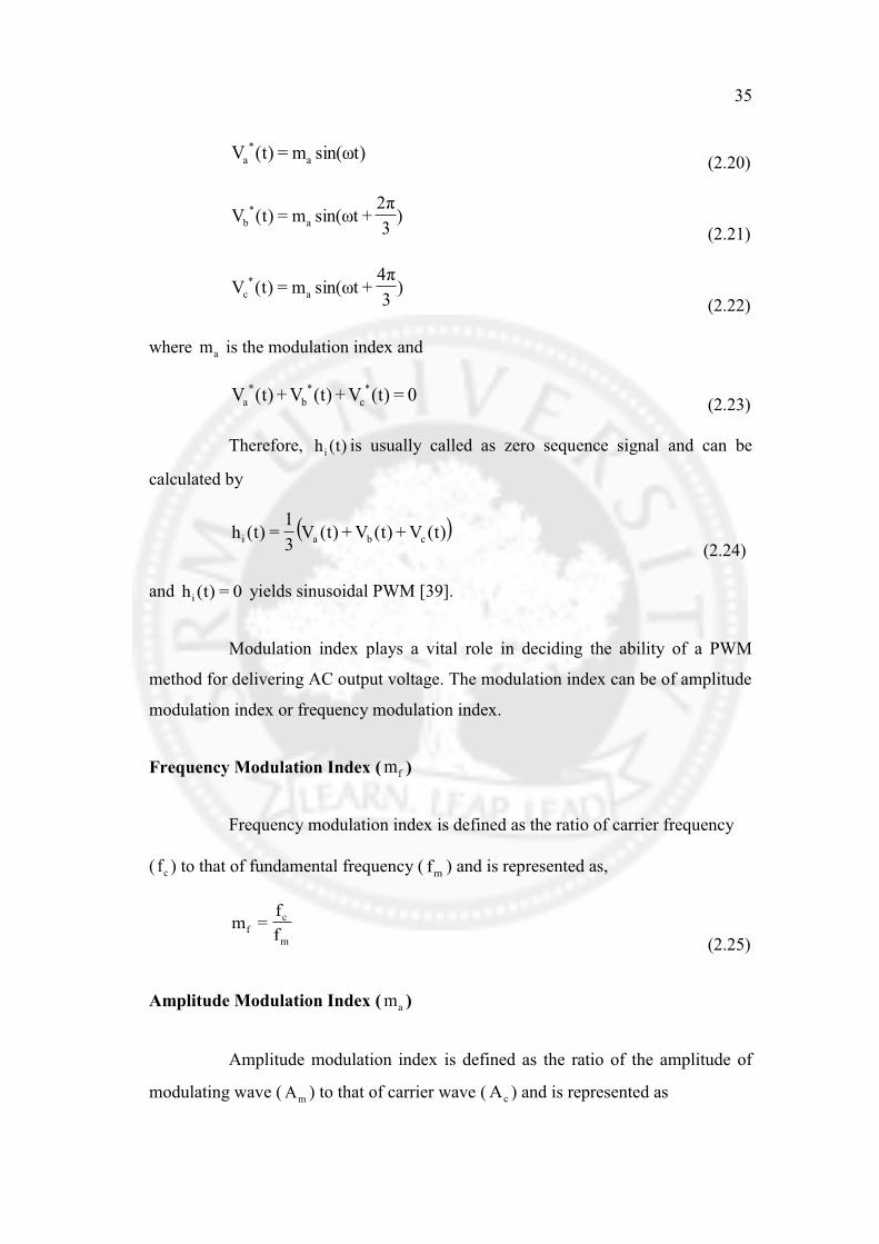
2.6.1.1 Phase Disposition Pulse Width Modulation (PD PWM)
The phase disposition PWM with single reference is based on the
comparison of a sinusoidal reference wave form with m-1 carriers which are
vertically shifted. For a five level output, in case of bipolar arrangement, this
technique uses two carriers which are present above the zero reference and two other
below the zero reference. As it can be seen from Figure 2.6 the carriers that have the
same frequency fc and amplitude Ac are in phase. The modulating sinusoidal wave
has a frequency of fr and an amplitude Ar.
Figure 2.6 Carrier arrangements for PD PWM with single reference
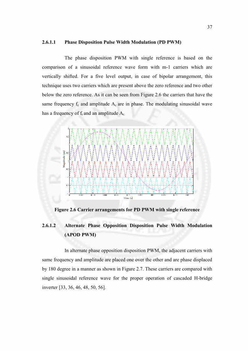
2.6.1.2 Alternate Phase Opposition Disposition Pulse Width Modulation
(APOD PWM)
In alternate phase opposition disposition PWM, the adjacent carriers with
same frequency and amplitude are placed one over the other and are phase displaced
by 180 degree in a manner as shown in Figure 2.7. These carriers are compared with
single sinusoidal reference wave for the proper operation of cascaded H-bridge
inverter [33, 36, 46, 48, 50, 56].

38
Figure 2.7 Carrier arrangements for APOD PWM with single reference
2.6.1.3 Phase Opposition Disposition Pulse Width Modulation (POD PWM)
The carrier waveforms with same amplitude and frequency are in phase
above and below the zero reference value. However, as shown in Figure 2.8, there is
180 degree phase shift between the ones above and below the zero reference. These
carriers are superimposed with single sine reference wave to generate the pulses for
controlling the switches of multilevel inverter.
Depending upon the nature of mf (odd triplen, even and even triplen),
their harmonic energies are predicted for five level cascaded H-bridge inverter.
Figure 2.8 Carrier arrangements for POD PWM with single reference
39
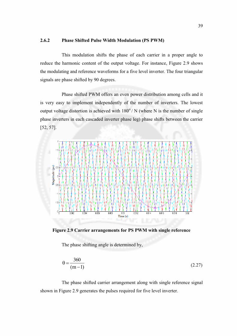
2.6.2 Phase Shifted Pulse Width Modulation (PS PWM)
This modulation shifts the phase of each carrier in a proper angle to
reduce the harmonic content of the output voltage. For instance, Figure 2.9 shows
the modulating and reference waveforms for a five level inverter. The four triangular
signals are phase shifted by 90 degrees.
Phase shifted PWM offers an even power distribution among cells and it
is very easy to implement independently of the number of inverters. The lowest
output voltage distortion is achieved with 180ο / N (where N is the number of single
phase inverters in each cascaded inverter phase leg) phase shifts between the carrier
[52, 57].
Figure 2.9 Carrier arrangements for PS PWM with single reference
The phase shifting angle is determined by,
)1m(360�
�� (2.27)
The phase shifted carrier arrangement along with single reference signal
shown in Figure 2.9 generates the pulses required for five level inverter.

40
2.6.3 Hybrid PWM Technique
In level shifted PWM technique, each carrier is associated with a specific
voltage level and cells are used only when the corresponding level is reached. This
produces uneven power distribution and switching conditions between the cells.
This increases the input current distortion. These harmonics can be important due to
the amount of power involved in high power applications.
In phase shifted PWM technique, since all the carriers are not in phase,
the output voltage has some additional dv/dt that is not produced by level shifted
methods. This leads to a higher and undesirable voltage distortion [51].
Hybrid PWM technique combines the features of PD and PS method.
Figure 2.10 shows a set of carrier signals which are used to generate the switching
pulses. In the positive half side, (m-1)/2 carriers are arranged in vertical offsets, i.e.
carriers are arranged one above the other and are in phase with each other. In the
negative half side, (m-1)/2 carriers are arranged in horizontal offsets which are
shifted at a particular angle. The interactions of these carriers with single reference
generate the gating signals [38, 50].
Figure 2.10 Carrier arrangements for hybrid PWM with single reference

41
2.7 SIMULATION RESULTS AND DISCUSSION
The main focus of this section is to develop PWM technique using
MATLAB / SIMULINK and to analyze the performance of three phase cascaded H-
bridge multilevel inverter under various modulation indices with single reference
signal. Simulation results for a five level inverter with level shifted and phase shifted
PWM are presented in this section.
Figure 2.11 Simulink diagram of single phase cascaded H-bridge multilevel inverter
Figure 2.12 Simulink model of three phase cascaded H-bridge five level inverter

42
For five level three phase system, shown in Figure 2.3, three control signals of different phase angles are needed. Three control signals for each phase are generated and compared with the carrier signals. Thus we get different sets of switching signals for different phases of the inverter.
Figure 2.13 Pulse generation circuit with single reference
.
Figure 2.14 Simulink model of single phase cascaded H-bridge five level inverter
The single phase circuit which is a part of a three phase system is shown in Figure 2.11. As shown in Figure. 2.12 and Figure. 2.14, three individual phase subsystems are needed to achieve the three phase output. Switching signal generators in the subsystem are completely independent of each other. Only the phase angles of the control signals are different.

43
For the five level inverter described in the section, four carrier signals of same frequency but different phases are needed. The carrier signals produced are then compared with the generated single reference using individual comparators and switching pulses for each switches are generated. It is clearly understood that the frequency of the control signal is 50Hz which is the desired frequency of the five-level inverter.
Figure 2.15 Five level cascaded H-bridge inverter phase voltage with single reference based PD PWM (ma = 0.9, mf = 63)
Figure 2.16 Phase voltage harmonic spectrum with single reference based PD PWM (ma = 0.9, mf = 63)
For each of the complementary switches, the pulses are generated by just inversing the corresponding pulses using individual NOT gate. The complete circuit diagram for generating eight switching pulses of a typical imbricated cells of single phase five level inverter with single reference signal is shown in Figure 2.13

44
Figure 2.17 Five level cascaded H-bridge inverter phase voltage with single reference based APOD PWM (ma = 0.9, mf = 63)
.
Figure 2.18 Phase voltage harmonic spectrum with single reference based APOD PWM (ma = 0.9, mf = 63)
Figure 2.19 Five level cascaded H-bridge inverter phase voltage with single reference based POD PWM (ma = 0.9, mf = 63)

45
Figure 2.20 Phase voltage harmonic spectrum with single reference based POD PWM (ma = 0.9, mf = 63)
Figure 2.21 Five level cascaded H-bridge inverter phase voltage with single reference based PS PWM (ma = 0.9, mf = 63)
Figure 2.22 Phase voltage harmonic spectrum with single reference based PS PWM (ma = 0.9, mf = 63)

46
Figure 2.23 Five level cascaded H-bridge inverter phase voltage with single reference based hybrid PWM (ma = 0.9, mf = 63)
Figure 2.24 Phase voltage harmonic spectrum with single reference based hybrid PWM (ma = 0.9, mf = 63)
The performance of three phase cascaded multilevel inverter is analyzed
with the help of MATLAB / SIMULINK to verify that the designed inverter can
practically be implemented.
In the simulation study, it is assumed that the DC voltage input to each
module is Vdc = 100 V and the inverter load is of resistive – inductive in nature.

47
2.7.1 Calculation of Performance Parameters
1. Total Harmonic Distortion
The total harmonic distortion, which is a measure of closeness in shape
between a waveform and its fundamental component, is defined as
THD = 1
224
23
22
VV+........+V+V+V
(2.28)
2. Root Mean Square (RMS) Value
RMS Value = Periodcurve squared theunder Area
(2.29)
3. DC Voltage Utilization Rate (DCUR)
% DCUR = d
1
VV
(2.30)
where V1 denotes the fundamental output voltage & Vd represents the maximum
input DC voltage per phase.
4. Distortion Factor
Distortion factor is defined as the measure of effectiveness in reducing
unwanted harmonics without having to specify the values of a second order load
filter.
DF =2)THD(+1
1
(2.31)

48
5. Crest factor or Peak factor
Crest factor or Peak factor = Value RMSValue Peak
(2.32)
Table 2.4 %THD Vs PWM strategies for single reference
mf 63 120 200ma 0.9 0.8 0.7 0.9 0.8 0.7 0.9 0.8 0.7
APOD 19.07 22.62 23.92 15.19 15.57 19.29 33.17 38.09 41.46POD 19.15 22.61 23.71 15.23 15.55 19.32 33.18 38.08 41.53
Hybrid 22.25 27.15 31.54 14.58 14.96 18.99 37.58 44.08 51.48PD 19.06 22.71 23.86 15.31 15.56 19.22 33.28 38.12 41.52PS 8.35 9.37 10.24 22.62 26.07 27.50 31.76 36.11 39.16
Table 2.5 Crest factor Vs PWM strategies for single reference
mf 63 120 200ma 0.9 0.8 0.7 0.9 0.8 0.7 0.9 0.8 0.7
APOD 1.414 1.414 1.4144 1.4139 1.413 1.414 1.414 1.414 1.414POD 1.414 1.414 1.4139 1.4142 1.414 1.414 1.414 1.414 1.414
Hybrid 1.414 1.413 1.4144 1.4140 1.414 1.414 1.414 1.414 1.413PD 1.414 1.414 1.4144 1.4140 1.414 1.414 1.414 1.414 1.414PS 1.414 1.414 1.4140 1.4140 1.414 1.413 1.414 1.414 1.414
Table 2.6 %DC Voltage Utilization Rate (DCUR) Vs PWM strategies for single reference
mf 63 120 200ma 0.9 0.8 0.7 0.9 0.8 0.7 0.9 0.8 0.7
APOD 63.65 56.55 49.49 63.55 56.45 49.43 63.65 56.55 49.5POD 63.6 56.55 49.48 63.5 56.4 49.36 63.65 56.55 49.5
Hybrid 63.66 56.55 49.53 63.65 56.55 49.53 63.65 56.55 49.52PD 63.65 56.6 49.49 63.65 56.55 49.5 63.65 56.55 49.5PS 63.66 56.55 49.5 63.65 56.55 49.48 63.65 56.55 49.49

49
Table 2.7 RMS Values Vs for PWM strategies single reference
mf 63 120 200
ma 0.9 0.8 0.7 0.9 0.8 0.7 0.9 0.8 0.7
APOD 127.3 113.1 98.98 127.09 112.9 98.86 127.3 113.1 99.00
POD 127.2 113.1 98.95 127.00 112.8 98.71 127.3 113.1 98.99
Hybrid 127.31 113.1 99.05 127.29 113.1 99.06 127.3 113.1 99.03
PD 127.29 113.2 98.98 127.29 113.1 98.99 127.3 113.1 98.99
PS 127.31 113.1 99.00 127.29 113.1 98.96 127.3 113.1 98.98
Table 2.8 %Distortion factor Vs PWM strategies for single reference
mf 63 120 200ma 0.9 0.8 0.7 0.9 0.8 0.7 0.9 0.8 0.7
APOD 5.236 4.416 4.1770 6.5691 6.3364 5.1771 3.0134 2.6245 2.4113
POD 5.214 4.418 4.2139 6.5519 6.4176 5.1691 3.0125 2.6252 2.4072
Hybrid 4.485 3.680 3.1690 6.8426 6.6696 5.2586 2.6600 2.2680 1.9421
PD 5.239 4.399 4.1874 6.5178 6.4135 5.1959 3.0035 2.6224 2.4078
PS 11.891 10.611 9.7194 4.4166 3.8330 3.6340 3.1471 2.7683 2.5528
Analyses are carried out based on the RMS value of the output phase
voltage, DCUR, DF, CF and harmonic spectrum obtained from the CHB five level
inverter.
Figure 2.15 shows the phase output voltage of PD PWM strategy (with
ma = 0.9, mf = 63). Figure 2.16 indicates the phase voltage harmonic spectrum for
PD strategy with single reference. It has a switching frequency of 3150Hz with a
fundamental frequency of 50Hz. At a modulation index of 0.9, the fundamental
output voltage obtained using PDPWM strategy is about 180V and has a total
harmonic distortion of 19.06%.
50
Figure 2.17 and Figure 2.18 display the phase voltage waveform and its
harmonic spectrum of APOD PWM strategy. The fundamental voltage is 179.9 V
and % THD is 19.07 for ma = 0.9, mf = 63.
Figure 2.19 and Figure 2.20 show the phase voltage and the FFT
spectrum of the output voltage with POD PWM strategy. For ma = 0.9, mf = 63, the
POD PWM strategy based five level inverter produces a fundamental voltage of
179.9V with a %THD of 19.15.
The phase voltage and the harmonic spectrum of PS PWM are shown in
Figure 2.21 and Figure 2.22 which confirm an output fundamental voltage of
179.9V and %THD of 8.35 for ma = 0.9, mf = 63.
The hybrid PWM which is developed due to the combined effect of PD
and PS provides a fundamental voltage of 180.1V and % THD of 22.25. This is
illustrated in Figure 2.23 and Figure 2.24.
Further analysis on the output voltage is carried out by varying amplitude
modulation index and frequency modulation index.
Total harmonic distortion decreases and RMS output voltage increases as
ma increases which is depicted by Table 2.4 and Table 2.7 respectively. From the
output voltage spectrum, %DCUR has been calculated using equation 2.30 and this
is found to increase with increase in ma, but it remains constant for any variations in
mf. Similarly crest factor has been estimated by equation 2.32 and is found to be
1.414 for all PWM strategies irrespective of any variations in modulation indices.
Table 2.5 depicts the above said concept and illustrates that the obtained output
voltage approaches sine wave.
A comparison of the waveforms and spectra shown in Figure 2.15-
Figure 2.24 confirms that all level shifted PWM techniques show a similar
performance. It is also understood from the above discussion that the phase shifted
PWM shows a better performance when compared with other multicarrier PWM
techniques.

51
2.8 SUMMARY
This chapter presents a review of the state of the art and developments of multilevel voltage source inverters. The analyzed operating principles and special features exhibit specific technical advantages and disadvantages which justify their presence in the market. The increasing technical requirements of high / medium voltage applications require substantial efforts and research of multilevel inverters. From the above discussion, it can be understood that for research on multilevel inverter topologies, a preferred topology is expected to have the following characteristics:
� Ability of expanding the level easily
� No voltage balancing problem
� Modular structure
As cascaded multilevel inverter meets all the above said characteristics, in this dissertation, cascaded multilevel inverter is considered as the test bench for investigating different PWM strategies.
Apart from the review of multilevel inverter, in this chapter, analysis has been carried out to determine the suitable multicarrier PWM technique with single reference. After careful examination, by varying modulation index, it has been concluded that among various pulse width modulation techniques analyzed in the above section, phase shifted pulse width modulation technique with single reference has shown a better performance profile when compared with all other multicarrier PWM techniques.