z-source inverter application in grid-tied pv systems · z-source inverter application in grid-tied...
TRANSCRIPT
Z-Source Inverter Application in Grid-Tied PV
Systems
Ricardo Santana
Técnico Lisboa / DEEC
University of Lisbon
Lisboa, Portugal
Abstract— This paper proposes the application of the new
converter topology, named Z-Source Inverter, on the power
conditioning of a PV source with a three wire and transformers-
less grid connection. This converter topology has a LC filter with
X configuration, allowing the inverter to operate in the Shoot-
Through mode, making the inverter resistant to EMI phenomena
and establishing the unique feature of single stage DC link
voltage boost. For the power control, a high velocity AC current
mode MPPT is proposed. The AC current is modulated by
hysteresis controller with adaptive band, limited frequency and
unit power factor. The unconditional current controllability is
achieved by a dual loop capacitor voltage control. The operation
of the proposed system is tested by simulation and the evaluation
of performance is made, considering the incident radiation
intermittence and the “Shadow Effect”, which is considered one
of the mains problems within this type of systems.
Keywords- Z-Source Inverter; PV source; three wire
transformer-less grid connection; high velocity MPPT; hysteresis
controller; unit power factor.
I. INTRODUCTION
The scarcity and increased prices of fossil fuels, as well as global warning concerns are responsible for the recent governmental support on the investments for exploration of renewable and non-polluting sources. The beginning of the XXI century is characterized by the strong development at world scale of this type of technology [1]. Within this framework, the solar photovoltaic systems (PV) take especial attention, with a rated grow of 42% in the 2012 [2].
Grid-Tied PV systems are taking an impressive development due to the governmental support and interesting rates. But, one of the main barriers for the massive exploration of this concept consists on the economics scales and unit price of the equipment. Also, this type of technology is associated with power conversion systems that represent a considerable rate of the investment. Investigation efforts have been taken in order to reduce the cost of power conversion stages, increase the overall efficiency and improvement of reliability. Another effort of investigation associated with this type of conversion systems consists on the development of new and improved control strategies in order to achieve a fast and stable dynamic response, since PV sources are affected by considerable levels of production potential intermittence.
In [3] a new power converter topology, named Z-Source Inverter, is proposed. This topology is very promising in alternative energy sources, allowing the power conversion in a single stage, with a unique buck/boost capability of the AC voltage established by the Shoot-Through command of the inverter, which is not possible in traditional topologies. The cost of semiconductors and control systems can be reduced and the system reliability is improved.
This paper proposes the application of the ZSI as a single stage power conditioning in three wires, transformer less, grid-tied PV sources. A new strategy of system control is also proposed, concerning various aspects: the intermittence of the production potential associated with this type of electrical sources and imposed by the radiation values; the unconditional stability and reliability of the overall power conversion system; the restrictions on the energy quality associated with grid-tied converters and fast dynamic performance.
In section II, a state of the art and fundamental concepts analysis is described. In section III, a theoretical analysis of the operating principle and a small signal model of the converter are presented. A detailed description of the proposed systems with individual explanation on the control elements is presented in section IV. In order to verify the accuracy of the proposed analysis and system design and performance, simulation in Matlab/Simulink™ environment is shown in section V. The conclusions are presented in section VI.
II. FUNDAMENTAL CONCEPTS AND STATE OF THE ART
A. Photovoltaic Systems
Due to non-linear behaviour of the PV cell, a power conditioning unit is needed in order to extract the maximum power available, named Maximum Power Point Tracker (MPPT). Typically, this unit is implemented by the association of a DC-DC converter plus a logical algorithm. Controlling the conduction state of the converter’s semiconductors, it is possible to control the power extracted from de PV source.
A MPPT algorithm establishes the logic for the control of conduction duty cycle. The Perturb and Observe (P&O) and Incremental Conductance (Inc Cond), due to their high performance, are the most common methods in literature [4-5]. The main drawback of the P&O method consists on the power value oscillations around the maximum power point (MPP), the amplitude of the oscillations depends on the algorithm step size. The Inc Cond, comparing the distance of the operation point with the MPP, can establish the operation point at maximum power without oscillation. However, both methods suffer from the fixed step size problem. For a large step size, the set up time is small, but the solution point may not be achieved. For a shorter step size, the solution is assured but the set up time is increased [5].
For grid-tied applications, an additional DC-AC converter is needed. Typically, this last conversion stage is composed by a full-bridge voltage source inverter (VSI). This converter operates with eight permissible modes. Each mode is described by an equivalent space vector. The vectors V1 to V6 represent the operation of the inverter in an Active state and the DC link voltage is partially applied to the output phases. The vectors V0 and V7 represent de operation of the inverter in an Open state and a null voltage is applied to the output phases. At this point,
a voltage Buck characteristic of the inverter is verified. In order to establish the conventional power flow from the source to the grid, in some cases, a minimum DC link voltage has to be assured. This fact imposes the straight dependence of the VSI in association with a DC-DC Boost converter. In some applications, a step down transformer is used in the inverter’s output to minimize the DC link voltage requirement. However, the power unit cost of the systems is highly increased [6].
Another drawback associated with the topologies described before consists on the need for “Times Gaps” while designing the inverter, in order to avoid the simultaneous conduction of two switches in the same leg. This peculiar operation, named Shoot-Through will result in the equipment lost due to a short-circuit of a DC voltage source or capacitor. This fact causes the inverter to be vulnerable to Electromagnetic Interference (EMI).
B. Z-Source Inverter
Considering the verified limitations of conventional VSI topologies or association with DC-DC converter, Z. Peng proposes in 2003 [3] the new converter topology named Z-Source Inverter. This converter employs an unique LC impedance with X configuration to couple the power circuit to the electrical source. The configuration of the filter allows the operation of the VSI in the Shoot-Through (ST) mode. This operation mode, not allowed in traditional topologies, establish the unique feature of single stage output voltage Buck/Boost capability
The unique features verified on the ZSI topology, makes it desirable for application in any type of power conversion systems, with especial attention to DC-AC conversion systems. The application of the ZSI in automotive drivers is studied in [7-9]. One of the main investigations concerns it’s the application of the ZSI as power conditioner within photovoltaic sources supplying loads or connected to the electrical grid [10-15].
In spite of the evident advantages given by the allowed ST operation mode, the same will affect the VSI modulation process. In fact, this feature requires the implementation of modified Pulse With Modulation (PWM) strategies. This subject is considered another investigation concern, resulting in different PWM strategies with ST command [16-20]. The main drawback of the proposed control systems consist on the dependency of ST command availability with the modulation index, which constraint the voltage Boost control.
The dynamic control of the ZSI in different applications domains is also investigated. The most common strategy consists on the ST duty cycle control in order to achieve a minimum DC link voltage or capacitor voltage. This concept it’s achieved with a single feedback control strategy [21-24]. In [24] a dual loop capacitor voltage is proposed considering the current overload verified in the previous proposed control systems. For the purpose of dynamic control design, a small signal model of the converter is present in [25-27]. This model, not only gives the necessary transfer functions for controller design, but it also gives the information about de dynamic behaviour of the converter.
III. OPERATIONAL PRINCIPLE ANALYSIS
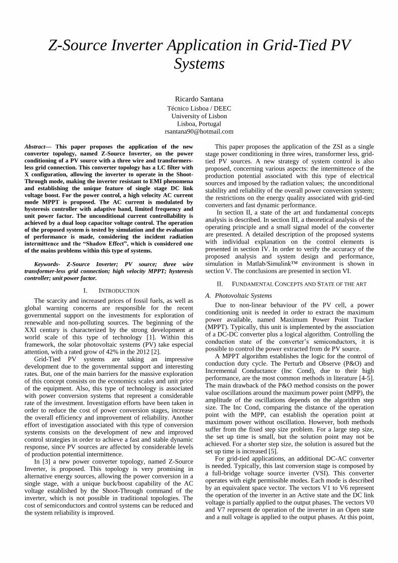
In this section, a steady state analysis and converter design method is presented. The AC model that describes the dynamic behaviour of the converter, based on the small signal analysis and space averaging, is also presented. The considered ZSI circuit is given in Figure 1.
Figure 1 Basic ZSI converter circuit
In this analysis, a symmetrical impedance network of the converter it’s considered.
(1)
(2)
Based on this consideration, the following simplifications can be established:
( ) ( ) ( ) (3)
( ) ( ) ( ) (4)
A. Steady State Analysis
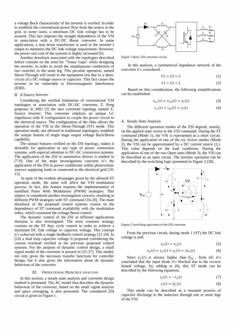
The different operation modes of the ZSI depend, mainly, on the applied state vector to the VSI command. During the ST command (Mode 1), the VSI is represented as a short circuit. During the application of one of the six Active modes (Mode 2), the VSI can be approximated by a DC current source ( ). This value depends on the load conditions. During the application of one of the two Open sates (Mode 3), the VSI can be described as an open circuit. The inverter operation can be described by the switching logic presented in Figure 2 [28].
Figure 2 Switching equivalent of the ZSI converter
From the previous circuit, during mode 1 (ST) the DC link voltage is null.
( ) ( ) (5)
( ) ( ) ( ) ( ) (6)
Since ( ) is always higher than , from (6) it’s concluded that the input diode it’s blocked due to the reverse biased voltage. So, adding to (6), this ST mode can be described by the following equations.
( ) ( ) (7)
( ) ( ) (8)
This mode can be described as a resonant process of capacitor discharge to the inductors through one or more legs of the VSI.
VDC
1
2
3
VSI
vi
Ii
vLvC
vC vL
L C
C L
D1
vd
iL
iC
iC
iin
iC
During mode 2 (Active) the input current of the VSI is equal to the DC current value and from the circuit analysis, (9) is obtained. ( ) ( ) (9)
Since the ZSI is operating as a voltage Boost, the inductor’s current is higher than the output DC current value. Considering this fact and (9) the conduction of the input diode it’s concluded. From the analysis of the circuit, the Active mode is described by the following equations.
( ) ( ) ( ) (10)
( ) ( ) (11)
The Open mode it’s considered as an Active mode with the particularity of a null VSI input current.
In steady state, the mean value of the capacitor current and inductor’s voltage measured in a switching period are null. Using this concept the conversion relationships that indicate the voltage boost capability as function of the ST duty cycle ( ) are obtained [3].
(12)
(13)
(14)
Were and represents the mean value of the capacitors and the peak DC link voltage, respectively. The indicates the mean value of the inductors current.
B. Impedance Design
The design of the impedance network is based on the ripple value of the capacitors voltage and inductors current on steady state. The converter is switched at a frequency and the input source power is .
For the design of the capacitors, constant inductors current and a voltage ripple factor are considered. During the ST mode, the ripple amplitude of the capacitors voltage is given by .(15).
(15)
Combining the last equation with (14), the capacitance value is expressed by (16).
( )
( )
(16)
For the inductors design, constant capacitor voltage and a current ripple factor are considered. During the ST mode, the ripple amplitude of the inductors current is given by (17).
(17)
Combining the (17) with (12), the inductance value is expressed by (18).
( )
( ) (18)
C. Dynamic Modelling
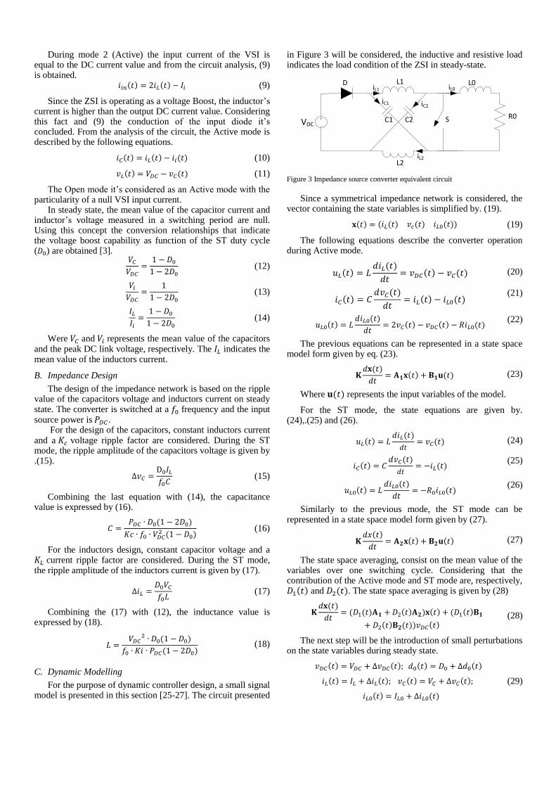
For the purpose of dynamic controller design, a small signal model is presented in this section [25-27]. The circuit presented
in Figure 3 will be considered, the inductive and resistive load indicates the load condition of the ZSI in steady-state.
Figure 3 Impedance source converter equivalent circuit
Since a symmetrical impedance network is considered, the vector containing the state variables is simplified by. (19).
( ) ( ( ) ( ) ( )) (19)
The following equations describe the converter operation during Active mode.
( ) ( )
( ) ( ) (20)
( )
( )
( ) ( )
(21)
( )
( )
( ) ( ) ( )
(22)
The previous equations can be represented in a state space model form given by eq. (23).
( )
( ) ( ) (23)
Where ( ) represents the input variables of the model.
For the ST mode, the state equations are given by. (24),.(25) and (26).
( ) ( )
( ) (24)
( )
( )
( )
(25)
( )
( )
( )
(26)
Similarly to the previous mode, the ST mode can be represented in a state space model form given by (27).
( )
( ) ( ) (27)
The state space averaging, consist on the mean value of the variables over one switching cycle. Considering that the contribution of the Active mode and ST mode are, respectively, ( ) and ( ). The state space averaging is given by (28)
( )
( ( ) ( ) ) ( ) ( ( )
( ) ( )) ( ) (28)
The next step will be the introduction of small perturbations on the state variables during steady state.
( ) ( ) ( ) ( )
( ) ( ) ( ) ( )
( ) ( )
(29)
VDC
L1
L2
C1 C2
L0
R0S
iL1
iL2
iL0
iC1 iC2
D
Appling the perturbations given by (29) with the averaged state space (28). A new state space model, having the ST duty cycle and voltage source perturbations as inputs is achieved (30) (on the bottom of the page). The main utility of this model is the formalization of the transfer functions, using Laplace transform, that relates the dynamic behaviour between the different state variables. For the controller design, only the transfer functions that relate the capacitor voltage and inductors currents variations with the ST duty cycle perturbations are considered, respectively ( ) and ( ) given by (31) and (32) at the bottom of the page [25-27].
IV. PROPOSED SYSTEM
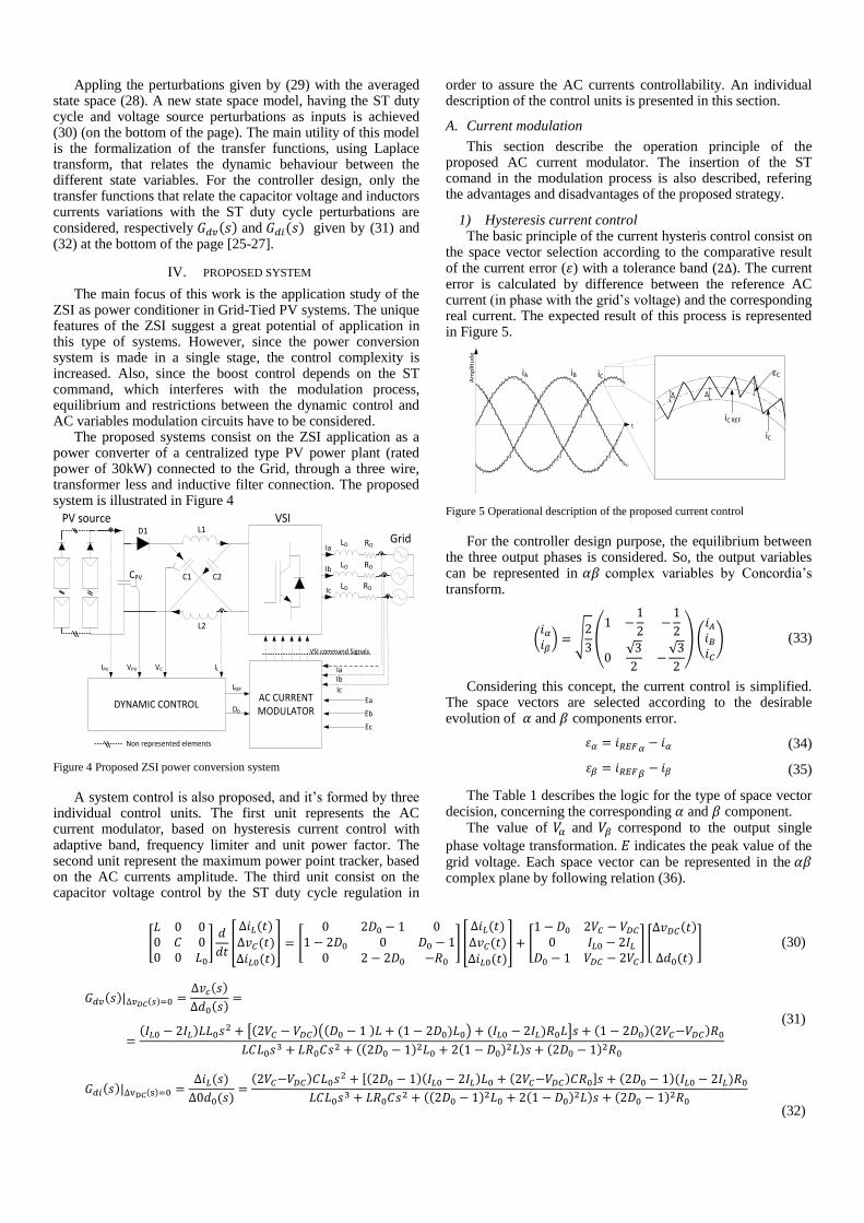
The main focus of this work is the application study of the ZSI as power conditioner in Grid-Tied PV systems. The unique features of the ZSI suggest a great potential of application in this type of systems. However, since the power conversion system is made in a single stage, the control complexity is increased. Also, since the boost control depends on the ST command, which interferes with the modulation process, equilibrium and restrictions between the dynamic control and AC variables modulation circuits have to be considered.
The proposed systems consist on the ZSI application as a power converter of a centralized type PV power plant (rated power of 30kW) connected to the Grid, through a three wire, transformer less and inductive filter connection. The proposed system is illustrated in Figure 4
Figure 4 Proposed ZSI power conversion system
A system control is also proposed, and it’s formed by three individual control units. The first unit represents the AC current modulator, based on hysteresis current control with adaptive band, frequency limiter and unit power factor. The second unit represent the maximum power point tracker, based on the AC currents amplitude. The third unit consist on the capacitor voltage control by the ST duty cycle regulation in
order to assure the AC currents controllability. An individual description of the control units is presented in this section.
A. Current modulation
This section describe the operation principle of the proposed AC current modulator. The insertion of the ST comand in the modulation process is also described, refering the advantages and disadvantages of the proposed strategy.
1) Hysteresis current control The basic principle of the current hysteris control consist on
the space vector selection according to the comparative result of the current error ( ) with a tolerance band ( ). The current error is calculated by difference between the reference AC current (in phase with the grid’s voltage) and the corresponding real current. The expected result of this process is represented in Figure 5.
Figure 5 Operational description of the proposed current control
For the controller design purpose, the equilibrium between the three output phases is considered. So, the output variables can be represented in complex variables by Concordia’s transform.
(
) √
(
√
√
)
(
) (33)
Considering this concept, the current control is simplified. The space vectors are selected according to the desirable evolution of and components error.
(34)
(35)
The Table 1 describes the logic for the type of space vector decision, concerning the corresponding and component.
The value of and correspond to the output single
phase voltage transformation. indicates the peak value of the grid voltage. Each space vector can be represented in the complex plane by following relation (36).
L1
L2
C1 C2
LO RO
LO
LO
RO
RO
D1
DYNAMIC CONTROLAC CURRENT MODULATOR
IREF
D0
Ea
Eb
Ec
Ia
Ib
Ic
IaIb
Ic
VSI command Signals
IPV VPV VC IL
CPV
Non represented elements
Grid
PV source VSI
t
Am
pli
tud
e
Δ Δ
εC
iC
iC REF
iA iB iC
𝐿 𝐶 𝐿
𝑑
𝑑𝑡
𝑖𝐿(𝑡)
𝑣𝐶(𝑡) 𝑖𝐿 (𝑡)
𝐷 𝐷 𝐷
𝐷 𝑅
𝑖𝐿(𝑡)
𝑣𝐶(𝑡) 𝑖𝐿 (𝑡)
𝐷 𝑉𝐶 𝑉𝐷𝐶 𝐼𝐿 𝐼𝐿
𝐷 𝑉𝐷𝐶 𝑉𝐶
𝑣𝐷𝐶(𝑡)
. 𝑑 (𝑡)
(30)
𝐺𝑑𝑣(𝑠)| 𝑣𝐷𝐶(𝑠)= 𝑣𝑐(𝑠)
𝑑 (𝑠)
(𝐼𝐿 𝐼𝐿)𝐿𝐿 𝑠
( 𝑉𝐶 𝑉𝐷𝐶) (𝐷 )𝐿 ( 𝐷 )𝐿 (𝐼𝐿 𝐼𝐿)𝑅 𝐿 𝑠 ( 𝐷 )( 𝑉𝐶 𝑉𝐷𝐶)𝑅
𝐿𝐶𝐿 𝑠3 𝐿𝑅 𝐶𝑠
(( 𝐷 ) 𝐿 ( 𝐷 ) 𝐿)𝑠 ( 𝐷 ) 𝑅
(31)
𝐺𝑑𝑖(𝑠)| vDC(s)= 𝑖𝐿(𝑠)
𝑑 (𝑠)
( 𝑉𝐶 𝑉𝐷𝐶)𝐶𝐿 𝑠 ( 𝐷 )(𝐼𝐿 𝐼𝐿)𝐿 ( 𝑉𝐶 𝑉𝐷𝐶)𝐶𝑅 𝑠 ( 𝐷 )(𝐼𝐿 𝐼𝐿)𝑅
𝐿𝐶𝐿 𝑠3 𝐿𝑅 𝐶𝑠
(( 𝐷 ) 𝐿 ( 𝐷 ) 𝐿)𝑠 ( 𝐷 ) 𝑅
(32)

Case Error
condition
Desirable current
evolution
Type of space
vector
A
B
C
Table 1 Logic associated with the space vector decision
(36)
Figure 6 Space vectors representation on plane
The association of Figure 6 with the logic presented in Table 1 result in the space vector decision for each case, as shown in Table 2.
Case A B C
A V2 V1 V6
B V2,V3 V0,V7,ST V5,V6
C V3 V4 V5
Table 2 Space vector decision for each case
From the analysis of Table 2, vector decision ambiguities, caused by the fact that has non null value, can be identified. These ambiguities can be solved if the proximity of to the tolerance band borders is known. Considering this fact, the split of the tolerance band in upper and lower band is proposed.
(37)
(38)
To implement this concept, three comparators for each and component are used. The association of the three comparators result in an equivalent hysterics comparator Figure 7.
Since the combination of the comparators outputs result in four cases, the comparators states data can be treated as 4bits binary logic. And after the vector attribution for each area of decision, a binary logic can be implemented for the command of the VSI.
Since tolerance band is responsible for the current ripple around the reference value, if a fixed band weight is considered, the total harmonic distortion as an inverse proportional relationship with the reference AC current. In
order to reduce this effect and adaptive band is considered based on (37).
Figure 7 Equivalent hysteresis comparator and the decision areas
. (39)
This type of modulation process is characterised by a variable frequency. In the worst scenario, the VSI switching frequency may achieved the physical limit of operation, and at high frequencies, the switching lost become significant. Considering this fact, a frequency limiter using Flip Flop D is used.
2) Shoot-Through command The ST operation mode has maximum priority relatively to
the other eight permissible states. This feature allow the ST command to be independent of the normal modulation process, which has the advantage of maximum availability for this command and the frequency of the same command is also independent of the normal modulation variable frequency. The Figure 8, describe the ST command circuit, where indicate the conduction state of a VSI leg (obtained from the normal modulation process), and represent the semiconductor’s
gate signals.
Figure 8 ST command circuit
The main short come of this strategy consists on the modulation process distortion. During the ST application over the normal modulation process, the AC current suffers from perturbations caused by the grid voltage. The maximum amplitude of these perturbations it’s given by (38).
(40)
The apparent solution is to increase the ST command frequency ( ), but the DC link voltage availability is reduced, with a minimum value equal to the impedance capacitor voltage. For this reason, the AC current controllability is achieved by the capacitor voltage control. The reference value for the capacitor voltage control is determined by the AC side first harmonic analysis.
(41)
D0
1 γ1
γ2
γ3
S11
S21
S12
S22
S13
S23
ST 3
braços
D0
Mod.Normal
Mod.Normal
Mod.Normal
Mod.Normal
ST 3
braços
ST 3
braços
ST 3
braços
In the previous equation indicates the first harmonic
of the output single phase voltage. It can be related, by approximation, with the DC link voltage using the SPWM command relationship and a unitary modulation index (40).
(42)
Considering a high ST command frequency, the DC link voltage availability is reduced to the capacitor voltage. Adding a safety factor (
), the reference value for the capacitor
voltage control is given by (41).
√( ) (43)
B. Dynamic Control
For grid connected PV systems, the associated power converters must be characterized by a fast dynamic response due to considerable production potential intermittence imposed by the radiation values. In this type of systems, two primordial functions are considered for the dynamic controller. The first is related to the maxim point power tracking, due to the non-ideal behaviour of the PV source. The second refers to the DC-link voltage control using Buck/Boost feature of the associated converter.
For the proposed application, an AC current mode MPPT is proposed based on the Inc Cond algorithm [4-5]. The PV source current is controlled indirectly by the AC currents reference. Different reference values have different DC link voltage requirements. This concept leads to the second control unit. The required DC link voltage is controlled indirectly by a dual loop capacitor voltage control [24], using the reference voltage given in (41).
The proposed control system is presented in Figure 9.
Figure 9 Proposed dynamic control strategy
Since the state variables affect simultaneously the performance of the two control units. One unit performance is affected by the other. Considering this concept, a complementary operational routine is established by a decision Flip Flop JK. If a fast dynamic response is attributed to the MPPT control unit, an interaction signal (STN) between the two control units as to be used in order to assure the AC current controllability.
1) MPPT As described by the Incremental Conductance method [4-
5], the maximum power is reached if the (42) is verified.
(44)
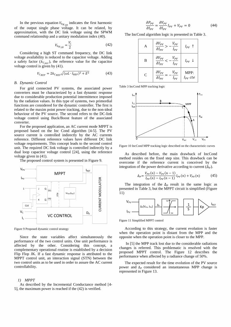
The IncCond algorithm logic is presented in Table 3.
A
B
C
MPP:
Table 3 IncCond MPP tracking logic
Figure 10 IncCond MPP tracking logic described on the characteristic curves
As described before, the main drawback of IncCond method resides on the fixed step size. This drawback can be overcome if the reference current is conceived by the integration of the power derivative according to current ( ).
( ) ( )
( ) ( ) ( ) ( ) (45)
The integration of the result in the same logic as presented in Table 3, but the MPPT circuit is simplified (Figure 11)
Figure 11 Simplified MPPT control
According to this strategy, the current evolution is faster when the operation point is distant from the MPP and the opposite when the operation point is closer to the MPP.
In [5] the MPP track lost due to the considerable radiations changes is referred. This problematic is resolved with the proposed MPPT control. The Figure 12 describes the performance when affected by a radiance change of 50%.
The expected result for the time evolution of the PV source power and considered an instantaneous MPP change is represented in Figure 13.
MPPT
VC CONTROL
J
K
Q
Q
1
CLK
CU
RR
ENT
MO
DU
LATO
R
IREF
D0
VcREF(IREF)
STN
VC
VPV
IPV
IL
EN1
EN2
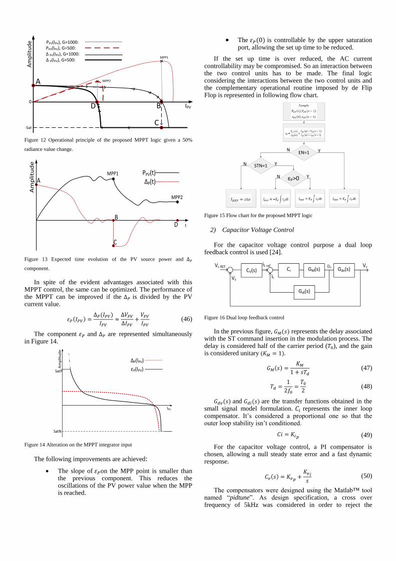
Figure 12 Operational principle of the proposed MPPT logic given a 50%
radiance value change.
Figure 13 Expected time evolution of the PV source power and
component.
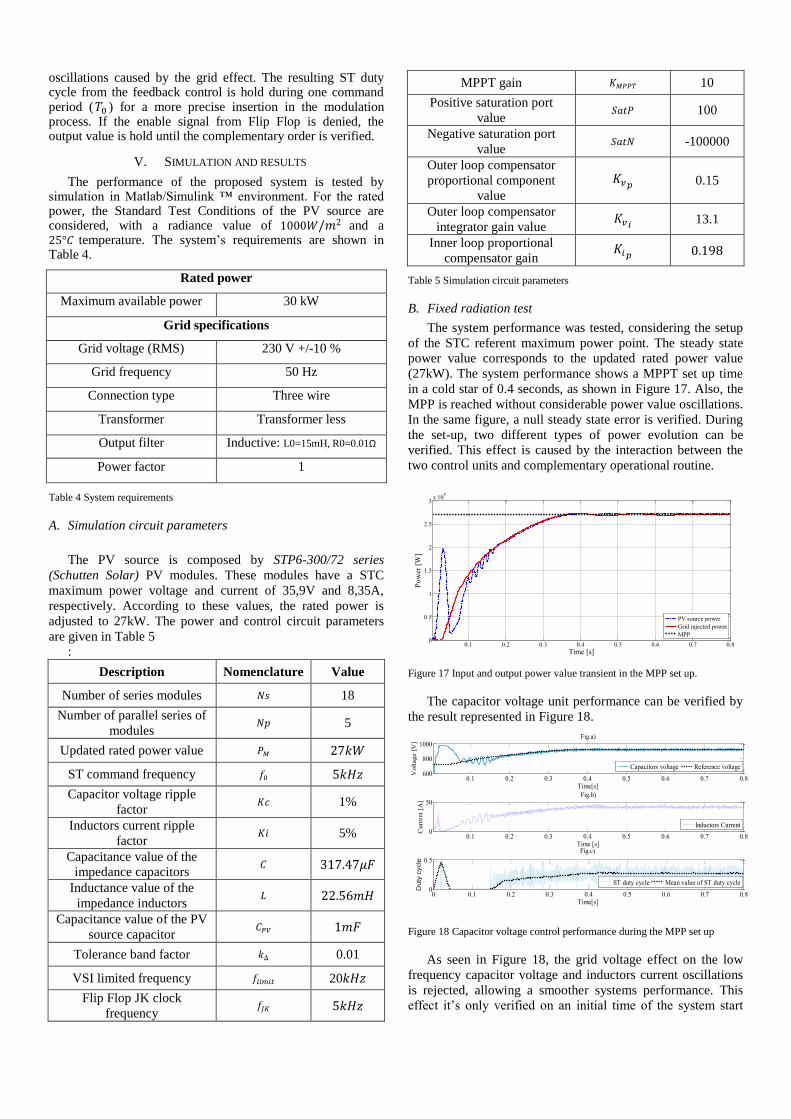
In spite of the evident advantages associated with this MPPT control, the same can be optimized. The performance of the MPPT can be improved if the is divided by the PV current value.
( ) ( )
(46)
The component and are represented simultaneously in Figure 14.
Figure 14 Alteration on the MPPT integrator input
The following improvements are achieved:
The slope of on the MPP point is smaller than the previous component. This reduces the oscillations of the PV power value when the MPP is reached.
The ( ) is controllable by the upper saturation port, allowing the set up time to be reduced.
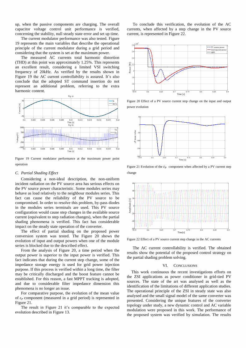
If the set up time is over reduced, the AC current controllability may be compromised. So an interaction between the two control units has to be made. The final logic considering the interactions between the two control units and the complementary operational routine imposed by de Flip Flop is represented in following flow chart.
Figure 15 Flow chart for the proposed MPPT logic
2) Capacitor Voltage Control
For the capacitor voltage control purpose a dual loop
feedback control is used [24].
Figure 16 Dual loop feedback control
In the previous figure, ( ) represents the delay associated with the ST command insertion in the modulation process. The delay is considered half of the carrier period ( ), and the gain is considered unitary ( ).
( )
(47)
(48)
( ) and ( ) are the transfer functions obtained in the small signal model formulation. represents the inner loop compensator. It’s considered a proportional one so that the outer loop stability isn’t conditioned.
(49)
For the capacitor voltage control, a PI compensator is chosen, allowing a null steady state error and a fast dynamic response.
( )
(50)
The compensators were designed using the Matlab™ tool named “pidtune”. As design specification, a cross over frequency of 5kHz was considered in order to reject the
MPP2
MPP1
-Sat
A
B
C
D
Am
plit
ud
e
IPV
PPV(IPV), G=1000:
0
PPV(IPV), G=500:Δ PV(IPV), G=1000:Δ P(IPV), G=500:
A
B
C
D
Am
pli
tud
e
t
MPP1
MPP2
PPV(t)ΔP(t)
Am
pli
tud
e
IPV
ΔP(IPV)
εP(IPV)SatP
SatN
EN=1
STN=1
εP>0
Y
Y
YN
N
N
oscillations caused by the grid effect. The resulting ST duty cycle from the feedback control is hold during one command period ( ) for a more precise insertion in the modulation process. If the enable signal from Flip Flop is denied, the output value is hold until the complementary order is verified.
V. SIMULATION AND RESULTS
The performance of the proposed system is tested by simulation in Matlab/Simulink ™ environment. For the rated power, the Standard Test Conditions of the PV source are considered, with a radiance value of and a temperature. The system’s requirements are shown in Table 4.
Rated power
Maximum available power 30 kW
Grid specifications
Grid voltage (RMS) 230 V +/-10 %
Grid frequency 50 Hz
Connection type Three wire
Transformer Transformer less
Output filter Inductive: L0=15mH, R0=0.01Ω
Power factor 1
Table 4 System requirements
A. Simulation circuit parameters
The PV source is composed by STP6-300/72 series
(Schutten Solar) PV modules. These modules have a STC
maximum power voltage and current of 35,9V and 8,35A,
respectively. According to these values, the rated power is
adjusted to 27kW. The power and control circuit parameters
are given in Table 5
:
Description Nomenclature Value
Number of series modules 18
Number of parallel series of
modules 5
Updated rated power value
ST command frequency
Capacitor voltage ripple
factor 1%
Inductors current ripple
factor 5%
Capacitance value of the
impedance capacitors .
Inductance value of the
impedance inductors .
Capacitance value of the PV
source capacitor
Tolerance band factor 0.01
VSI limited frequency 20
Flip Flop JK clock
frequency
MPPT gain 10
Positive saturation port
value 100
Negative saturation port
value -100000
Outer loop compensator
proportional component
value
0.15
Outer loop compensator
integrator gain value
13.1
Inner loop proportional
compensator gain
.
Table 5 Simulation circuit parameters
B. Fixed radiation test
The system performance was tested, considering the setup
of the STC referent maximum power point. The steady state
power value corresponds to the updated rated power value
(27kW). The system performance shows a MPPT set up time
in a cold star of 0.4 seconds, as shown in Figure 17. Also, the
MPP is reached without considerable power value oscillations.
In the same figure, a null steady state error is verified. During
the set-up, two different types of power evolution can be
verified. This effect is caused by the interaction between the
two control units and complementary operational routine.
Figure 17 Input and output power value transient in the MPP set up.
The capacitor voltage unit performance can be verified by
the result represented in Figure 18.
Figure 18 Capacitor voltage control performance during the MPP set up
As seen in Figure 18, the grid voltage effect on the low
frequency capacitor voltage and inductors current oscillations
is rejected, allowing a smoother systems performance. This
effect it’s only verified on an initial time of the system start
0.1 0.2 0.3 0.4 0.5 0.6 0.7 0.80
0.5
1
1.5
2
2.5
3x 10
4
Time [s]
Po
wer
[W
]
PV source power
Grid injected power
MPP
0.1 0.2 0.3 0.4 0.5 0.6 0.7 0.8600
800
1000
Time[s]
Vo
ltag
e [
V]
Fig.a)
Capacitors voltage Reference voltage
0.1 0.2 0.3 0.4 0.5 0.6 0.7 0.80
50
Time [s]
Cu
rren
t [A
]
Fig.b)
Inductors Current
0 0.1 0.2 0.3 0.4 0.5 0.6 0.7 0.80
0.5
Time[s]
Duty
cycle
Fig.c)
ST duty cycle Mean value of ST duty cycle
up, when the passive components are charging. The overall
capacitor voltage control unit performance is verified,
concerning the stability, null steady state error and set up time.
The current modulator performance was also tested. Figure
19 represents the main variables that describe the operational
principle of the current modulator during a grid period and
considering that the system is set at the maximum power.
The measured AC currents total harmonic distortion
(THD) at this point was approximately 1.25%. This represents
an excellent result, considering a limited VSI switching
frequency of 20kHz. As verified by the results shown in
Figure 19 the AC current controllability is assured. It’s also
conclude that the adopted ST command insertion do not
represent an additional problem, referring to the extra
harmonic content.
Figure 19 Current modulator performance at the maximum power point
operation
C. Partial Shading Effect
Considering a non-ideal description, the non-uniform
incident radiation on the PV source area has serious effects on
the PV source power characteristic. Some modules series may
behave as load relatively to the neighbour modules series. This
fact can cause the reliability of the PV source to be
compromised. In order to resolve this problem, by-pass diodes
in the modules series terminals are used. This PV source
configuration would cause step changes in the available source
current (equivalent to step radiation changes), when the partial
shading phenomena is verified. This fact has considerable
impact on the steady state operation of the converter.
The effect of partial shading on the proposed power
conversion system was tested. The Figure 20 shows the
evolution of input and output powers when one of the module
series is blocked due to the described effect.
From the analysis of Figure 20, a time period when the
output power is superior to the input power is verified. This
fact indicates that during the current step change, some of the
impedance storage energy is used for grid power injection
purpose. If this process is verified within a long time, the filter
may be critically discharged and the boost feature cannot be
established. For this reason, a fast MPPT tracking is adopted,
and due to considerable filter impedance dimension this
phenomena is no longer an issue.
For comparative purpose, the evolution of the mean value
of component (measured in a grid period) is represented in
Figure 21.
The result in Figure 21 it’s comparable to the expected
evolution described in Figure 13.
To conclude this verification, the evolution of the AC
currents, when affected by a step change in the PV source
current, is represented in Figure 22.
Figure 20 Effect of a PV source current step change on the input and output
power evolution
Figure 21 Evolution of the component when affected by a PV current step
change
Figure 22 Effect of a PV source current step change in the AC currents
The AC current controllability is verified. The obtained
results show the potential of the proposed control strategy on
the partial shading problem solving.
VI. CONCLUSIONS
This work continuous the recent investigations efforts on
the ZSI applications as power conditioner in grid-tied PV
sources. The state of the art was analysed as well as the
identification of the limitations of different application studies.
The operational principle of the ZSI in steady state was also
analysed and the small signal model of the same converter was
presented. Considering the unique features of the converter
topology under study, a new dynamic control and AC variable
modulation were proposed in this work. The performance of
the proposed system was verified by simulation. The results
0.6 0.602 0.604 0.606 0.608 0.61 0.612 0.614 0.616 0.618 0.62-1000
-500
0
500
1000
Time [s]
Volt
age[V
]
Fig. b)
Va
Ea
0.6 0.602 0.604 0.606 0.608 0.61 0.612 0.614 0.616 0.618 0.62
-50
0
50
Time [s]
Curr
ent
[A]
Fig. a)
Ia
Iref a
0.55 0.6 0.65 0.7 0.75 0.8 0.85 0.91.4
1.6
1.8
2
2.2
2.4
2.6
2.8x 10
4
Time [s]
Po
wer
[W]
PV source power
Grid injected power
MPP
0.55 0.6 0.65 0.7 0.75 0.8 0.85 0.9-200
-150
-100
-50
0
50
Time [s]
P m
ean
val
ue
0.55 0.6 0.65 0.7 0.75 0.8 0.85 0.9-60
-40
-20
0
20
40
60
Time[s]
Am
pli
tud
e [
A]

show the capability of the proposed system for resolving some
of the main issues associated with the power system under
study.
REFERENCES
[1] International Energy Agency, "Renewables in global energy supply," An
IEA Fact Sheet, Janeiro 2007.
[2] REN21, "Renewables 2013," Global Status Report, 2013.
[3] Fang Zheng Peng, "Z-Source Inverter," , vol. 39, 2003.
[4] Seon-Ju Ahn, Joon-Ho Choi, Won-Wook Jung, Sang-Yun Yun, Il-Keun Song Seok-Il Go, "Simulation and Analysis of Existing MPPT Control Methods," Journal of International Council on Electrical Engineering, vol. 1, pp. 446-451, 2011.
[5] David Sanz Morales, "Maximum Power Point Tracking Algorithms for Photovoltaic Applications," Faculty of Electronics, Communications and Automation, Finland, Thesis for the Master of Sciences and Technology degree. 2010.
[6] Prajna Paramita Dash, "A High-Performance Three-Phase Grid-Connected PV System Based On Multilevel Current Source Inverter," University of Waterloo, Waterloo, Ontario, Canada, Ph.D. Thesis 2013.
[7] Alan Joseph, Jin Wang, Member, Fang Z. Peng, Donald J. Adams Miaosen Shen, "Comparison of Traditional Inverters and Z-Source Inverter for Fuel Cell Vehicles," IEEE Trans. Power Electron, vol. 22, July 2007
[8] Rhafael de Sousa Moretti, "Estudo e implementação de um conversor CC-CC baseado no Z-Source alimentado por células de combustivel ," Universidade Federal de Santa Catarina, Florianópolis, Master Thesis 2007.
[9] Joeri Van Mierlo Omar Ellabban, "Z-Source Inverter for Automotive Applications," in New Generation of Electric Vehicles.: InTech, ch. 10
[10] Miaosen Shen, Fang Z. Peng, Jin Wang Yi Huang, "Z-Source Inverter for Residential Photovoltaic Systems," IEEE Trans Power Electron., vol. 21, 2006
[11] Sengodan Thangaprakash, "Unified MPPT Control Strategy for Z-Source Unified MPPT Control Strategy for Z-Source Systems," Journal of Power Electronics, vol. 12, 2012.
[12] Shahrokh Farhangi Babak Farhangi, "Application of Z-Source Converter in Photovoltaic Grid-Connected Transformer-Less Inverter," Journal Electrical Power Quality and Utilisation , vol. 12, 2006.
[13] Chen Yan, Gan Yuanxing, Zhou Lin Guo Ke, "Control of Z-Source Photovoltaic Inverter for Grid-Connected Based on Constant-Frequency Hysteresis Current Control," in IEEE 37th Photovoltaic Specialists Conference, Seattle, WA, 2011.
[14] Surin Khomfoi, Prapart Paisuwanna Anucha Pattanaphol, "Z-Source Grid-Connected Inverter for Interfacing With Photovoltaic Cells," in The
8th Electrical Engineering/ Electronics, Computer,Telecommunications and Information Technology Association, Thailand, 2011.
[15] Qin Chao Xunjiang Dai, "The Research of Photovoltaic Grid-Connected Inverter Based on Adaptive Current Hysteresis Band Control Scheme," Xinjiang University, China
[16] Anwen Shen, Phan Quoc Dzung, Nguyen Bao Anh, Nguyen Xuan Phu Cong-Thanh Pham, "A Comparison of Control Methods for Z-Source Inverter," Energy and Power Engineering, vol. 4, pp. 187-195, 2012.
[17] D. Mahinda Vilathgamuwa, Yue Sen Lai, Geok Tin Chua,Yunwei Li Poh Chiang Loh, "Pulse-Width Modulation of Z-Source Inverters," IEEE Trans.Power Electron, vol. 20, 2005.
[18] Jin Wang, Alan Joseph, Fang Zheng Peng, Leon M. Tolbert, Donald J. Adams Miaosen Shen, "Maximum Constant Boost Control of the Z-Source Inverter," IAS, 2004.
[19] A. Krishnan S. Thangaprakash, "Modified Space Vector Pulse Width Modulation for Z-Source Inverters," International Journal of Recent Trends in Engineering, vol. 2, 2009.
[20] Miaosen Shen, Zhaoming Qian Fang Zheng Peng, "Maximum Boost Control of the Z-Source Inverter," IEEE Trans. Power Electron., vol. 20, 2005.
[21] M. Veerachary T. Chandrashekhar, "Control of Single-Phase Z-source Inverter for a Grid Connected System," in Third International Conference on Power Systems, Kharagpur, INDIA, 2009.
[22] Zhaoming Qian, Shuitao Yang, Bin Cui, Fang Zheng Peng Xinping Ding, "A PID Control Strategy for DC-link Boost Voltage in Z-source Inverter," in Applied Power Electronics Conference - Twenty Second Annual IEEE, 2007.
[23] S. Mirzakuchaki, S. M. J. Rastegar Fatemi M. J. Rastegar Fatemi, "Wide-Range Control of Output Voltage in Z-source Inverter by Neural Network," in International Conference on Electrical Machines and Systems, 2008.
[24] Joeri Van Mierlo Omar Ellabban, "Capacitor Voltage Control Techniques of the Z-source Inverter: A Comparative Study," EPE Journal, vol. 21, 2011
[25] Jiangang Hu, Longya Xu Jingbo Liu, "Dynamic Modeling and Analysis of Z Source Converter—Derivation of AC Small Signal Model and Design-Oriented Analysis," IEEE Trans.Power Electron., vol. 22, 2007
[26] Gokhan Sen, "Voltage and current programmed modes in control of the z source converter," The Graduate Faculty of The University of Akron, Master Thesis 2008.
[27] D. Mahinda Vilathgamuwa, Chandana Jayampathi Gajanayake, Yih Rong Lim, Chern Wern Teo Poh Chiang Loh, "Transient Modeling and Analysis of Pulse-Width Modulated Z-Source Inverter," IEEE Trans. Power Electron., vol. 22, 2007.
[28] Laksumana Jayawickrama Sumedha Rajakaruna, "Steady-State Analysis and Designing Impedance Network of Z-Source Inverter," IEEE Trans Ind. Electron., vol. 57, July 2010.