wood, stone, and vinyl via soft ... - kaust...
TRANSCRIPT
Non-Planar Nano-Scale Fin Field Effect Transistors on Textile,Paper, Wood, Stone, and Vinyl via Soft Material-Enabled
Double-Transfer Printing
KAUSTRepository
Item type Article
Authors Rojas, Jhonathan Prieto; Sevilla, Galo T.; Alfaraj, Nasir;Ghoneim, Mohamed T.; Kutbee, Arwa T.; Sridharan,Ashvitha; Hussain, Muhammad Mustafa
Citation Non-Planar Nano-Scale Fin Field Effect Transistors onTextile, Paper, Wood, Stone, and Vinyl via Soft Material-Enabled Double-Transfer Printing 2015:150501111031008ACS Nano
Eprint version Post-print
DOI 10.1021/acsnano.5b00686
Publisher American Chemical Society (ACS)
Journal ACS Nano
Rights This document is the Accepted Manuscript version of aPublished Work that appeared in final form in ACS Nano,copyright © American Chemical Society after peer reviewand technical editing by the publisher. To access the finaledited and published work seehttp://pubs.acs.org/doi/abs/10.1021/acsnano.5b00686.
Downloaded 29-Apr-2018 07:17:54
Link to item http://hdl.handle.net/10754/552326
Subscriber access provided by King Abdullah University of Science and Technology Library
ACS Nano is published by the American Chemical Society. 1155 Sixteenth StreetN.W., Washington, DC 20036Published by American Chemical Society. Copyright © American Chemical Society.However, no copyright claim is made to original U.S. Government works, or worksproduced by employees of any Commonwealth realm Crown government in the courseof their duties.
Article
Non-Planar Nano-Scale Fin Field Effect Transistors on Textile, Paper,Wood, Stone, and Vinyl via Soft Material-Enabled Double-Transfer Printing
Jhonathan P Rojas, Galo A Torres Sevilla, Nasir Alfaraj, Mohamed T Ghoneim,Arwa T Kutbee, Ashvitha Sridharan, and Muhammad Mustafa Hussain
ACS Nano, Just Accepted Manuscript • DOI: 10.1021/acsnano.5b00686 • Publication Date (Web): 01 May 2015
Downloaded from http://pubs.acs.org on May 5, 2015
Just Accepted
“Just Accepted” manuscripts have been peer-reviewed and accepted for publication. They are postedonline prior to technical editing, formatting for publication and author proofing. The American ChemicalSociety provides “Just Accepted” as a free service to the research community to expedite thedissemination of scientific material as soon as possible after acceptance. “Just Accepted” manuscriptsappear in full in PDF format accompanied by an HTML abstract. “Just Accepted” manuscripts have beenfully peer reviewed, but should not be considered the official version of record. They are accessible to allreaders and citable by the Digital Object Identifier (DOI®). “Just Accepted” is an optional service offeredto authors. Therefore, the “Just Accepted” Web site may not include all articles that will be publishedin the journal. After a manuscript is technically edited and formatted, it will be removed from the “JustAccepted” Web site and published as an ASAP article. Note that technical editing may introduce minorchanges to the manuscript text and/or graphics which could affect content, and all legal disclaimersand ethical guidelines that apply to the journal pertain. ACS cannot be held responsible for errorsor consequences arising from the use of information contained in these “Just Accepted” manuscripts.
1
Non-Planar Nano-Scale Fin Field Effect
Transistors on Textile, Paper, Wood, Stone, and
Vinyl via Soft Material-Enabled Double-
Transfer Printing
Jhonathan P. Rojas,†,§ Galo A. Torres Sevilla,
†,§ Nasir Alfaraj,
† Mohamed T. Ghoneim,
†
Arwa T. Kutbee,† Ashvitha Sridharan,
‡ Muhammad Mustafa Hussain*
,†
† Integrated Nanotechnology Lab, King Abdullah University of Science and Technology,
Thuwal 23955-6900, Saudi Arabia
‡ The KAUST Schools, King Abdullah University of Science and Technology, Thuwal
23955-6900, Saudi Arabia
§Authors contributed equally to this work
KEYWORDS:
Double-transfer, Soft material, non-planar, FinFETs, Asymmetric surface.
Page 1 of 29
ACS Paragon Plus Environment
ACS Nano
123456789101112131415161718192021222324252627282930313233343536373839404142434445464748495051525354555657585960
2
ABSTRACT
The ability to incorporate rigid but high-performance nano-scale non-planar
complementary metal-oxide semiconductor (CMOS) electronics with curvilinear,
irregular, or asymmetric shapes and surfaces is an arduous but timely challenge in
enabling the production of wearable electronics with an in-situ information-processing
ability in the digital world. Therefore, we are demonstrating a soft-material enabled
double-transfer-based process to integrate flexible, silicon-based, nano-scale, non-planar,
fin-shaped field effect transistors (FinFETs) and planar metal-oxide-semiconductor field
effect transistors (MOSFETs) on various asymmetric surfaces to study their compatibility
and enhanced applicability in various emerging fields. FinFET devices feature sub-20 nm
dimensions and state-of-the-art, high-κ/metal gate stacks, showing no performance
alteration after the transfer process. A further analysis of the transferred MOSFET
devices, featuring 1 µm gate length, exhibits an ION value of nearly 70 µA/µm (VDS = 2 V,
VGS = 2 V) and a low sub-threshold swing of around 90 mV/dec, proving that a soft
interfacial material can act both as a strong adhesion/interposing layer between devices
and final substrate as well as a means to reduce strain, which ultimately helps maintain
the device’s performance with insignificant deterioration even at a high bending state.
Page 2 of 29
ACS Paragon Plus Environment
ACS Nano
123456789101112131415161718192021222324252627282930313233343536373839404142434445464748495051525354555657585960
3
Flexibility has become a key feature and game changer that allows not only large-scale
deployment of electronics in what is now known as macro-electronics1 but also offers the
possibility of integration of electronics with wavy, curvilinear, irregular, or asymmetric
shapes and surfaces, such as textile, paper, vinyl, wood, glass, stone, and tiles. This can
leverage the development of electronic display, lighting, distributed sensor networks,
large-surface energy harvesting (such as photovoltaic, thermoelectric generator, etc.), or
bio-integrated systems enabling the Internet of Everything.2–8
In the recent past, the
display industry has focused on making curved, large, flat-panel display screens. Organic
and polymeric materials as well as amorphous silicon (a-Si) and low-temperature poly-
crystalline silicon (LTPS)-based electronics, have played an important role in the
development of such display technologies.9–11
Moving forward, the development of new
and exciting flexible, stretchable, and wearable high-performance technologies is a
critical enabler for the Internet of Everything.1 Since continuous data transmission from
various wearable electronics to the cloud is acutely energy inefficient, involving
excessive power consumption through large-bandwidth wireless communication,
centralized massive data processing, and because of potential cyber-security issues due to
hacking and technical vulnerability, it is important to integrate in-situ data-processing
capability and storage in wearable electronics for energy-efficient functionality and
information management. In that regard, out of a wide variety of existing materials
(organic, molecular, nanoparticles, quantum dots, nanowires, nanotubes, thin film, etc.),
inorganic, thin film based electronics show the most reliable and effective high-
performance information-processing capability. Some significant challenges with such
electronics include their rigidity, and brittleness; therefore, it is essential to make them
Page 3 of 29
ACS Paragon Plus Environment
ACS Nano
123456789101112131415161718192021222324252627282930313233343536373839404142434445464748495051525354555657585960
4
lightweight and flexible without compromising their advantages of higher information-
processing ability, thermal stability, integration density, and energy efficiency (due to
sub-1 volt low-input operation). Their flexural rigidity can be reduced, and remarkable
flexibility may be attained in making them ultra-thin. Various methods12-16
have been
demonstrated with interesting applications, including two18-23
of our own where we
uniquely used the bulk mono-crystalline silicon (100), which holds 90 percent of the
electronics market share with pre-fabricated devices, retaining ultra-large-scale-
integration (ULSI) density to demonstrate flexible, ultra-high-performance, nano-scale,
non-planar FinFETs—semiconductor industry’s most advanced transistor. While these
methods are exciting, their non-planar, nano-scale features pose a difficult challenge for
integration with various asymmetric surfaces readily available in our daily life, including
textile, paper, wood, stone, and vinyl. Not only do these materials have irregular
curvilinear surfaces, mitigating stress—while preserving structural integrity in their
embodiment with flexible ultra-thin layered materials with sensitive nano-scale featured
devices—is demanding. Soft-materials can serve as both an interposing and an
encapsulation layer. D.-H. Kim et al., for example, demonstrated the transfer printing of
ultra-thin circuits on different materials and irregular surfaces.17
In continuation of such
pioneering work, we have now adapted a double-transfer technique onto soft materials
with embedded, nano-scale, non-planar, state-of-the-art FinFETs and MOSFETs on
asymmetric surfaces of textile, paper, wood, stone, and vinyl as a prime example of how
our digital world will take shape in the future after the heterogeneous integration of
traditional but quite mature and reliable CMOS technology with up-and-coming, transfer
techniques using soft materials as the prime enabling catalyst.
Page 4 of 29
ACS Paragon Plus Environment
ACS Nano
123456789101112131415161718192021222324252627282930313233343536373839404142434445464748495051525354555657585960
5
Results and Discussions:
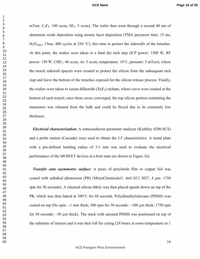
The hetero-integration process is shown in Figure 1. It begins with the release of a thin
layer of silicon of about 30 to 35 µm in thickness from a p-type (100) silicon wafer
(figure 1a). The procedure of extracting such a fabric consists of deep trench formation
followed by isotropic etching-based release, which has been demonstrated with various
devices and thicknesses (5-50 µm) by controlling various design parameters, such as the
trenches’ depth, as explained in detail in our previous works.25,26
The transfer process is
then carried out by placing the released silicon fabric upside-down on a piece of
polyimide film (Kapton) or copper foil, which is coated with unbaked photoresist (Figure
1b). The photoresist layer is meant to protect the topside of the fabric, where electronic
devices “sit”, and we have found that a thick layer is the most effective (above 2 µm).
Once the photoresist is baked, a thin layer of elastomer polydimethylsiloxane (PDMS) is
spin coated on top to provide final adhesion and isolation from applied strains (Figure
1c). The whole stack is then placed on top of the substrate of interest, and the PDMS
layer is left for curing (Figure 1d). Finally, the photoresist is dissolved with acetone to
release the carrier film/foil (Figure 1e). This double-transfer approach differentiates itself
from the standard single-transfer and printing approach, which relies on the mechanical
properties of nanomembranes with usually very small areas for single-device
development. In contrast, we offer the opportunity of large-area, complete-die transfer
with ultra-large-scale density capability.
We have chosen PDMS over other materials because of its favorable mechanical and
insulating properties as well as its biocompatibility demonstrated through its use in
several implants, bandages, contact lenses, and a variety of other medical uses.27
PDMS
Page 5 of 29
ACS Paragon Plus Environment
ACS Nano
123456789101112131415161718192021222324252627282930313233343536373839404142434445464748495051525354555657585960
6
can be considered as a variety of silicone: inert, synthetic compounds whose basic
structure is the inorganic compound of Si atoms with oxygen atoms (siloxane) and
methyl groups occupying the remaining free valences. Moreover, it is inexpensive,
transparent, and stretchable, and it can be conformably coated with a controlled thickness
in addition to its capacity to form mold structures with high resolutions.
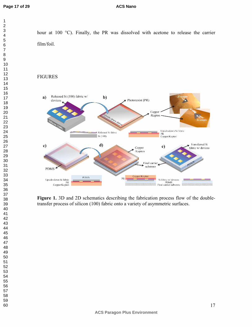
To demonstrate sophisticated non-planar devices, we have fabricated and transferred p-
type, state-of-the-art, 3D, non-planar, double-gate FinFET with improved electrostatic
control, featuring high-κ/metal gate materials and displaying exceptional electrical
performance and reduced short-channel effects. Starting up with an 8-inch silicon-on-
insulator (SOI) wafer, deep ultraviolet light (DUV) and resist trimming were used to
pattern the fins and thus achieve features down to 20 nm. Next, a reactive ion etching
(RIE) was used to anisotropically etch the silicon layer. Then, 20 nm of titanium nitride
(TiN) and 4 nm of hafnium dioxide (HfO2) formed the high-κ/metal gate stack, followed
by 200 nm of poly-silicon deposited by chemical vapor deposition (CVD). After gate
patterning, ion implantation was used to form source and drain; ohmic contacts were then
created with a silicidation process using nickel. Finally, aluminum contacts were formed
and a forming gas (N2/H2) anneal was performed at 420 °C. Once fabricated, the wafer
was diced and a die was selected for the soft back-etching process to thin the carrier
substrate down to 50 µm. Details on the thinning process can be found in our previous
publication.24
Next, the thin die was transferred onto a Kapton plastic with the previously
described procedure (Figure 2a). Figures 2b, 2c and 2d also display scanning and tunnel
electron microscopy (SEM and TEM) images with the detailed dimensions of the fins as
well as the output and transfer current-voltage (I-V) characteristics (Figures 2e and 2f) of
Page 6 of 29
ACS Paragon Plus Environment
ACS Nano
123456789101112131415161718192021222324252627282930313233343536373839404142434445464748495051525354555657585960
7
the fabricated device, comparing its behavior before and after the thinning and transfer
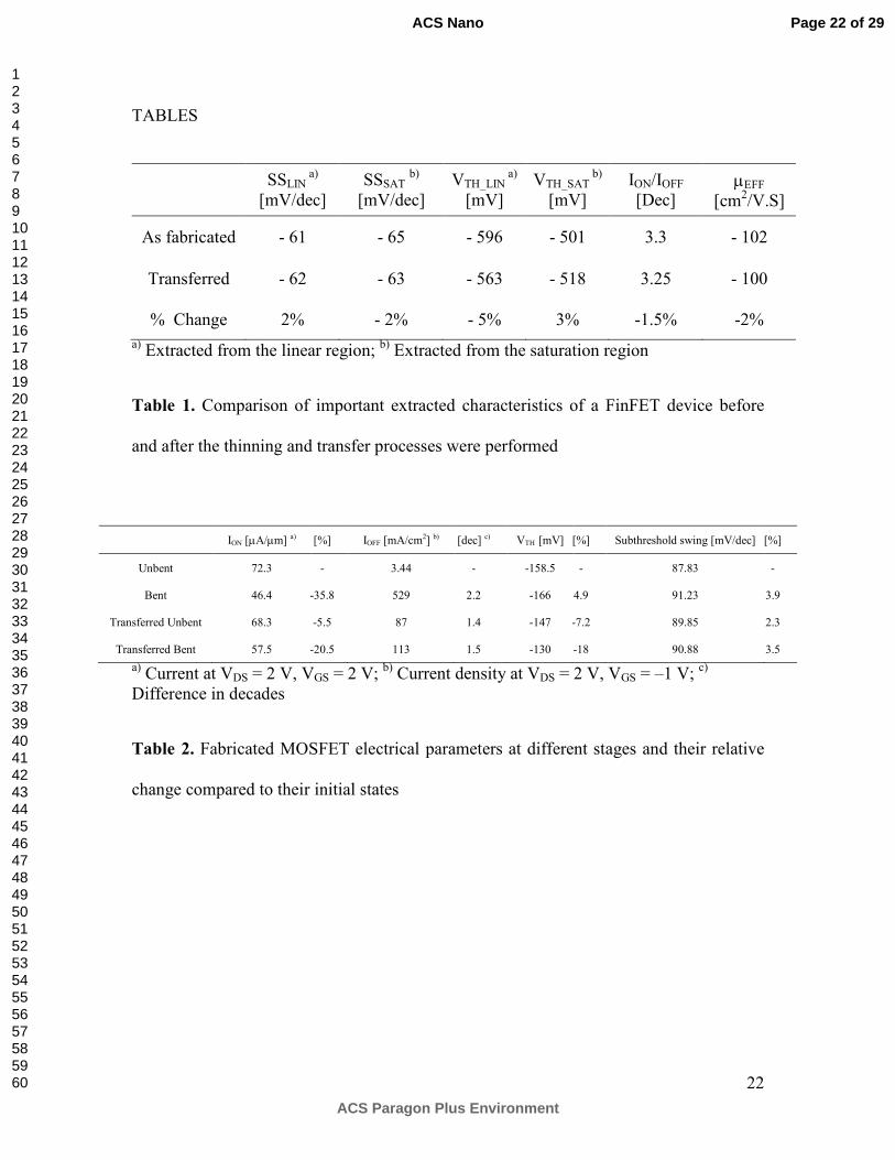
processes were carried out. Table 1 shows the comparison of several important extracted
parameters, which confirms there is only negligible change in performance once the
transfer process is completed. In the past, we have performed a more comprehensive
electrical study on how the mechanical motion of different bending radii (from 5 cm
down to 0.5 cm) affects the main electrical characteristics of the FinFETs (including
threshold voltage, subthreshold swing, effective mobility, transconductance, drain-
induced barrier lowering (DIBL), and gate delay and leakage current).24,28
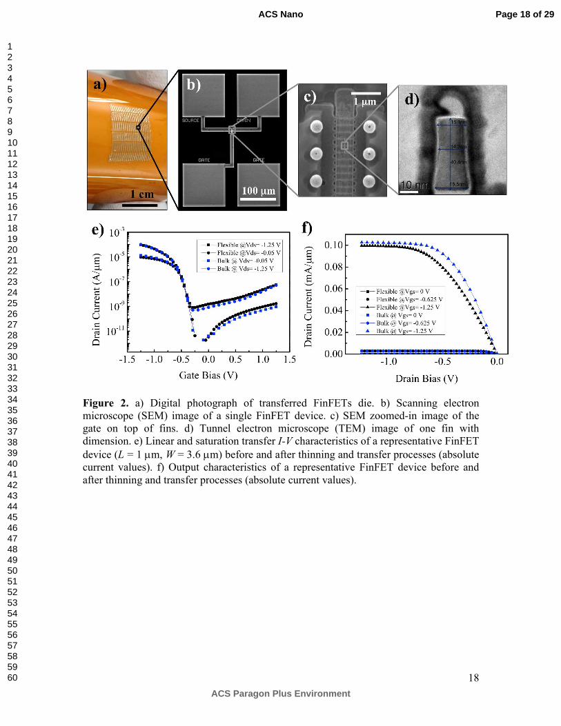
To further study the implications of the transfer process, we have additionally
fabricated and characterized n-type planar traditional MOSFETs, as they are the
dominant transistors in any advanced low-standby power (LSTP) and low-power (LOP)
circuitry. We made them flexible and semi-transparent through our trench-protect-
release-reuse-based process and then transferred them onto paper (Figure 3a) with the
purpose of examining the stress effect on the electrical behavior of the transistors. The
fabrication process started with the active area’s definition within a silicon dioxide
insulating layer, and then a gate stack was formed on top. The gate stack consisted of a
thin layer of silicon dioxide (20 nm SiO2) grown with thermal oxidation and
polycrystalline silicon (200 nm) and deposited with plasma-enhanced chemical vapor
deposition (PECVD). Gate dimensions were patterned with photolithography and RIE to
obtain features down to 1 µm (inset in Figure 4a). Silicon nitride spacers were formed to
protect the gate stack. Next, source and drain areas were created with ion implantation at
the gate’s sides. Nickel silicidation was then performed to improve contact resistance,
and finally aluminum contacts (200-nm-thick) were deposited with sputtering and then
Page 7 of 29
ACS Paragon Plus Environment
ACS Nano
123456789101112131415161718192021222324252627282930313233343536373839404142434445464748495051525354555657585960
8
patterned with RIE. Next, before carrying out the releasing process, the top exposed
silicon and poly-silicon areas were protected with a thin layer of Al2O3 deposited with
atomic layer deposition (ALD). The peel-off process was then performed as previously
described to separate a thin top layer (2 cm × 1 cm × ~40 µm) from the substrate with the
devices on top. Finally, the transfer process was carried out on a piece of paper with the
method explained previously.
Stress can play an important role in determining the transistor’s behavior, and one of
the key mechanisms in silicon is the piezoresistive effect, by which the bulk resistivity is
influenced by the mechanical stress applied to the material and how it is applied. From a
physical structure point of view, stress directly affects the bandgap distribution, which
causes changes in the effective mass of carriers. For electrons, stress causes redistribution
in the sub-bands, whereas, for holes, stress causes band split and deformation. Given that
mobility depends on the effective mass of carriers, stress can directly affect device
performance.29,30
On the other hand, only a small performance reduction was observed in
MOSFET devices after our CMOS-compatible peel-off process was performed,
compared with the on-wafer devices (where the most significant impact is on gate
leakage current) and at different applied strains (bending radii from 70 mm down to 5
mm or approximately 0.2% strain).21
Here, we have transferred a flexible silicon fabric
with MOSFET devices and characterized their performance before the transfer (flat and
bent to a radius of 3.5 mm) and after the transfer (flat and bent to a radius of 3.5 mm;
bending occurs in a longitudinal direction across the device channel). Figures 3b and 3c
show the I-V characteristics in the subthreshold and linear regions as well as leakage
current density. As can be observed, before the silicon fabric is transferred, bending
Page 8 of 29
ACS Paragon Plus Environment
ACS Nano
123456789101112131415161718192021222324252627282930313233343536373839404142434445464748495051525354555657585960
9
causes a noticeable detriment regarding on-state and gate leakage currents. We have
previously shown that flexibility can cause some electrical degradation in ultra-thin
flexible fabrics due to continuous mechanical stress, which is reflected in a high-
capacitance variation and increased interface defect density in the dielectric.31
It has been
previously demonstrated that the presence of defects in the dielectric leads to a higher
trap-assisted tunneling current, which at the same time produces an increment in leakage
current.32,33
But once our transfer process was performed, the impact of bending was
nearly eliminated when compared with the bare silicon fabric, which can be explained by
the strain reduction effect with the addition of the soft polymeric material. Table 2
summarizes the changes of important electrical parameters in the MOSFET device, and it
is evident that, after the transfer process, the device not only retained its functionality
with tolerable variations, but also recovered its performance and reduced strain-related
effects, with the additional observation that remaining defects in the dielectric will still
affect the gate leakage current, as observed in Figure 3d.
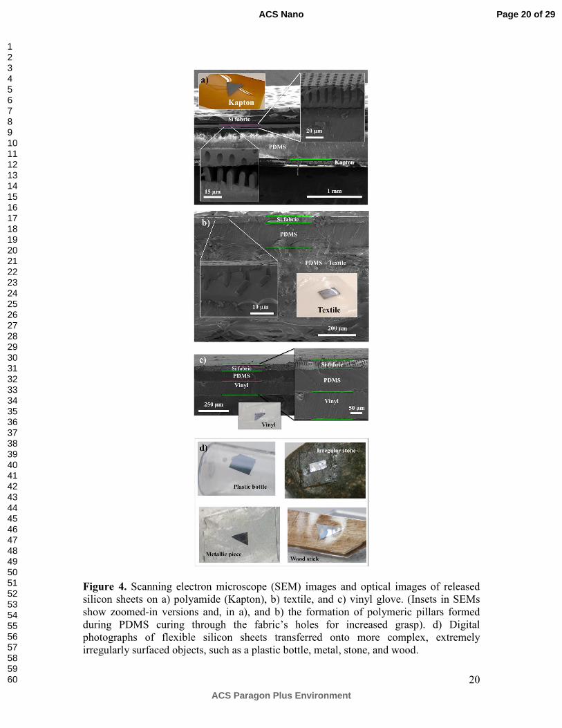
Regarding the mechanical characteristics of the transferred samples, we first observed
that different adhesion mechanisms were involved at the Si/PDMS and PDMS/substrate
interfaces. In the Si/PDMS interface, adhesion was promoted through trapping of the Si
sheet inside the cured PDMS. Figures 4a, 4b and 4c show scanning electron microscopy
(SEM) images of silicon fabrics (~30 µm in thickness) on top of the Kapton, textile, and
vinyl, showing how the PDMS penetrated up to the holes for better grip. But we also
observed that the penetration rate of PDMS into the substrate material increased rapidly
when the porosity of the substrate was increased. Textile (Figure 4b) and wood (Figure
4d) substrate materials exhibited strong adhesion to the Si sheet when compared with less
Page 9 of 29
ACS Paragon Plus Environment
ACS Nano
123456789101112131415161718192021222324252627282930313233343536373839404142434445464748495051525354555657585960

10
porous surfaces, such as Kapton or vinyl (Figures 4a and 4c). Thus, using PDMS was
expected to work for other materials because it provided an adhesion route independent
of the chemistry at both interfaces of Si/PDMS and PDMS/substrate. At the same time,
because of the strong adhesion, the main failure mechanism occurred from cracking at the
ultimate tensile strength of the fabric, rather than slipping or delamination, which have
been found to be a more common failure for relatively larger silicon thicknesses.14
Not only limited to adhesion promotion, the low modulus PDMS layer reduced the
applied strain on the silicon fabric. To appreciate this, the concept of mechanical neutral
surfaces must be considered. According to Suo et al. for materials with quite large
differences in the elastic moduli, the neutral surface between a Si sheet and an underneath
compliant material must shift from the mid-surface toward the compliant material.34
Since PDMS has a low elastic modulus of 0.5 MPa compared to the large elastic modulus
for silicon, the neutral surface must shift accordingly. Depending on the thicknesses of
both the Si sheet tSi and the PDMS tPDMS, their corresponding Young’s moduli YSi and
YPDMS, and R, the bending radius, a reduction of the applied strain on the Si sheet is
expected and governed by the relation34
:
���� =�������
�
��������
����������� (1)
where � = ���/����� and � = ���/�����. Thus, depending on the PDMS thickness it is
possible to control the reduction factor, as illustrated in Figure 5a, for different PDMS
thicknesses, achieving up to almost 20 times the strain reduction. This directly affects the
tensile strength of the system and helps achieve lower-bending radii for more compliant
fabrics. To illustrate this effect, we have compared the minimum bending radius of a
Page 10 of 29
ACS Paragon Plus Environment
ACS Nano
123456789101112131415161718192021222324252627282930313233343536373839404142434445464748495051525354555657585960
11
released ~10 µm silicon fabric with a transferred sample with similar dimensions. For a
PDMS thickness of around 50 µm, the sample achieved a bending radius as small as 1
mm (Figure 5b), compared to ~2 mm of the self-standing silicon fabric by itself.
On the other hand, adding a top encapsulating layer on the silicon sheet would not only
act as protection from diverse environmental conditions but it can also be adjusted so that
the neutral surface (where there is no strain) shifts to where the silicon substrate is
bending so that it does not add any strain to the electronic devices. This condition is met
when34
:
������� = ��� ���� �
� (2)
where Yencp and tencp are the young modulus and thickness of the encapsulating material.
In the case of a 30-µm-thick released silicon fabric, this value is about 120, which
corresponds to a PDMS thickness of approximately 15 µm. This same concept of
mechanical improvement by shifting of the encapsulating layer and neutral surface has
been previously studied by S.-I. Park et al.14
Transforming thin-film-based, traditional,
inorganic electronics by reducing their thickness is an effective way to achieve flexible
electronics—and using a PDMS-based support layer can lead to an effective way for
encapsulation of such electronics as a packaging layer.
Conclusions:
We have shown a generic hetero-integration of transfer printing and CMOS
technology-derived, state-of-the-art logic devices with both non-planar 3D FinFETs and
planar traditional MOSFETs on thin flexible substrates and a highly flexible mono-
Page 11 of 29
ACS Paragon Plus Environment
ACS Nano
123456789101112131415161718192021222324252627282930313233343536373839404142434445464748495051525354555657585960
12
crystalline silicon (100) fabric (derived from bulk substrate) to knit (weave) on various
wavy, curvilinear, irregular, or asymmetric surfaces (such as textile, paper, stone, wood,
vinyl, etc.) for wide deployment of high-performing, flexible electronics needed for
information processing, data distribution in distributed sensor networks, and other large-
surface-area, curvilinear electronic applications. The use of a soft polymeric material
gives us a way to not only provide a strong adhesion layer to reduce the strain and
achieve more compliant systems but also encapsulate ultra-thin, silicon fabric-based,
flexible electronics. Overall, transferring the silicon fabric with devices not only
facilitates handling and adds mechanical robustness but also helps reduce applied stress
to devices, which ultimately helps maintain their functioning performance with
insignificant deterioration even at a bending state.
METHODS
FinFET fabrication and thinning: The fabrication process began with an 8-inch
silicon-on-insulator (SOI) wafer (90 nm silicon on top of 125 nm BOX). The fins (15–20
nm width) were first patterned through deep ultra-violet lithography (DUV) and resist
trimming. Next, a high-κ/metal gate stack (4 nm of hafnium dioxide (HfO2) and 20 nm of
titanium nitride (TiN)) was formed through atomic layer deposition (ALD). Then, 200
nm of poly-silicon were deposited by chemical vapor deposition (CVD). A careful
etching process was performed to pattern the gate stack with no residual; then silicon
nitride (Si3N4) spacers were formed at each side of the gate. Next, to form the source and
drain, ion implantation (boron (B) in the case of p-type doped silicon) was used, followed
by activation annealing. Nickel silicidation (NiSi) was formed subsequently through
deposition of 15 nm of Ni, followed by 10 nm of TiN, then annealed at 450 °C. Inter-
Page 12 of 29
ACS Paragon Plus Environment
ACS Nano
123456789101112131415161718192021222324252627282930313233343536373839404142434445464748495051525354555657585960
13
layer dielectric (ILD) was formed with phosphosilicate glass (PSG) and plasma-enhanced
chemical vapor deposition (PECVD) silicon oxide (SiO2). Next, contact holes were
etched through the ILD, after which titanium (Ti) was deposited as a barrier layer, then
tungsten as plugs, and finally aluminum (Al) as contact pads. Further details can be found
in the corresponding author’s previous work.28-35
The thinning process can be
summarized as the anisotropic back-etching of a selected die through several steps of
deep reactive ion etching (DRIE) to adequately reach the desired thickness. A detailed
description of this process can also be found in our previous work.24
MOSFET fabrication: The fabrication started with lightly doped p-type 4-inch bulk Si
wafers. First, 300 nm of SiO2 was grown thermally using a dry-wet-dry oxidation
process. Next, the wafers were spin coated with diluted nLof 2070 photoresist to perform
the first lithography; the resist thickness due to dilution was coated to a thickness of 1 µm
(speed: 4000 rpm for 30 seconds, bake: 5 minutes at 100 ºC). Then, the exposure was
performed with research-level contact aligner EVG6200 with a constant dose of 300
mJ/cm2
and a post-exposure bake was performed (1 minute at 100 ºC). Resist
development was done for 1 minute in a 726 MIF developer. At this point, the wafers
were ready to perform the first etch step, which created the openings for the active area of
the transistor. The first etch was divided in two: anisotropic reactive ion etching to
remove the first 270 nm of SiO2 (ICP power: 1500 W, RF power: 150 W, CHF3: 40 sccm,
O2: 5 sccm, temperature: 10 ºC, pressure: 10 mTorr), followed by wet etch in buffered
oxide etchant (BOE) for 45 seconds to remove the remaining 30 nm of SiO2 without
damaging the Si surface. Next, the resist is removed in plasma asher (950 W of power,
100 sccm O2, 14 sccm Ar, temperature: 120 ºC, pressure: 500 mTorr). Then, the wafers
Page 13 of 29
ACS Paragon Plus Environment
ACS Nano
123456789101112131415161718192021222324252627282930313233343536373839404142434445464748495051525354555657585960
14
were cleaned in Piranha, SC1 and DHF before the gate stack oxide growth. The gate
oxide was grown thermally at 950˚C for 20 minutes of dry-oxidation to obtain a thickness
of 20 nm. Then, poly-Si was deposited on top of the wafer (temperature: 650˚C, pressure:
1000 mTorr, SiH4 flow: 50 sccm, Ar flow: 450 sccm, forward power: 10 W) for 5
minutes, obtaining a 200-nm-thick film. Next, the wafers went through a second
lithography step following the same steps as the ones performed for active definition. In
this step, the gate stack was defined and it was etched following two different steps: first,
poly-Si was etched using dry etching (ICP power: 250 W, RF power: 100 W,
temperature: 10˚C, pressure: 5 mTorr, HBr: 50 sccm, Cl2: 20 sccm). Second, the gate
oxide was removed with a timed wet BOE etch (30 seconds). Next, the resist was
removed with the same process as was done in the first resist removal. Then, 50 nm of
silicon nitride was deposited on top of the wafer (total time: 4 minutes, low frequency
pulse time: 6 seconds at 0.3 MHz, high frequency pulse time: 14 seconds at 13.56 MHz,
temperature: 300˚C, pressure: 850 mTorr, SiH4 flow: 23 sccm, NH3 flow: 20 sccm, N2
flow: 980 sccm, forward power: 20 W). The silicon nitride was then etched using a
combination of dry and wet etch to create the spacer; the first etch removed 45 nm of
Si3N4 (ICP power: 1500 W, RF power: 100 W, CHF3: 40 sccm, O2: 5 sccm, temperature:
10˚C, pressure: 10 mTorr), and the remaining 5 nm were removed with buffered oxide
etchant for 10 seconds. At this point, the wafers had the source and drain exposed and
were ready to be implanted. The wafers were implanted with arsenic ions with the
following conditions: dose = 4x10¹⁵
ions/cm2 and energy = 20 keV. Then, the wafers
were processed with vapor HF for 15 seconds to remove any native oxide. Next, 20 nm of
Ni were deposited on top of the wafers and annealed for 30 seconds at 450 ºC to create
Page 14 of 29
ACS Paragon Plus Environment
ACS Nano
123456789101112131415161718192021222324252627282930313233343536373839404142434445464748495051525354555657585960
15
NiSi and eliminate contact resistance between the aluminum pads and the source, drain
and gate contacts. The remaining nickel was then removed using Piranha. Next, 200 nm
of Al were deposited on top of the wafers, and a third lithography process was performed
using the same procedure as the first two lithography steps. At this point, the photoresist
defined the contact pads and source, drain, and gate connections. Then, a combination of
dry and wet etch was performed to define the aluminum pads and contacts; dry etch
(temperature: 80 °C; Step 1: ICP power: 1500W, RF power: 50 W, pressure: 40 mTorr,
Cl2: 10 sccm, BCl3: 40 sccm, Ar: 10 sccm; Step 2: ICP power: 1500 W, RF power: 150
W, pressure: 20 mTorr, Cl2: 40 sccm, BCl3: 10 sccm; Step 3: ICP power: 1500 W, RF
power: 50 W, pressure: 40 mTorr, Cl2: 10 sccm, BCl3: 30 sccm, Ar: 20 sccm; Step 4: RF
power: 150 W, pressure: 900 mTorr, O2: 100 sccm) was performed for 1 minute to
remove the first 150 nm of aluminum and 1 minute of wet etch in standard Al etchant
removed the remaining aluminum without damaging the silicon surface. Next, 40 nm of
aluminum oxide were deposited with atomic layer deposition (TMA precursor time: 15
ms, H2Ovapor: 15ms, 400 cycles at 250 °C) to protect the top silicon and poly-Si exposed
surfaces. A fourth and final lithography step was then performed on the wafers using ECI
3027 photoresist (spin speed: 1750 rpm, bake: 1 minute at 100˚C) to define the silicon
etch holes. The wafers went through two different dry etch steps: the first one removed
the 300 nm of SiO2 from the etch holes (ICP power: 1500 W, RF power: 150 W, CHF3:
40 sccm, O2: 5 sccm, temperature: 10˚C, pressure: 10 mTorr), and the second created
deep trenches (~ 45 µm) in the silicon wafer (90 cycles, temperature: ─20 °C; etch step: 7
seconds, ICP power: 1300 W, RF power: 30 W, pressure: 35 mTorr, C4F8: 5 sccm, SF6:
120 sccm; deposition step: 5 seconds, ICP power: 1300 W, RF power: 5 W, pressure: 35
Page 15 of 29
ACS Paragon Plus Environment
ACS Nano
123456789101112131415161718192021222324252627282930313233343536373839404142434445464748495051525354555657585960
16
mTorr, C4F8: 100 sccm, SF6: 5 sccm). The wafer then went through a second 40 nm of
aluminum oxide deposition using atomic layer deposition (TMA precursor time: 15 ms,
H2Ovapor: 15ms, 400 cycles at 250 °C), this time to protect the sidewalls of the trenches.
At this point, the wafers were taken to a final dry etch step (ICP power: 1500 W, RF
power: 150 W, CHF3: 40 sccm, Ar: 5 sccm, temperature: 10˚C, pressure: 5 mTorr), where
the trench sidewall spacers were created to protect the silicon from the subsequent etch
step and leave the bottom of the trenches exposed for the silicon release process. Finally,
the wafers were taken to xenon difluoride (XeF2) etchant, where caves were created at the
bottom of each trench; once these caves converged, the top silicon portion containing the
transistors was released from the bulk and could be flexed due to its extremely low
thickness.
Electrical characterization: A semiconductor parameter analyzer (Keithley 4200-SCS)
and a probe station (Cascade) were used to obtain the I-V characteristics. A metal plate
with a pre-defined bending radius of 3.5 mm was used to evaluate the electrical
performance of the MOSFET devices at a bent state (as shown in Figure 3a).
Transfer onto asymmetric surface: A piece of polyimide film or copper foil was
coated with unbaked photoresist (PR) (MicroChemicals©, 4ml ECI 3027, 4 µm: 1750
rpm for 30 seconds). A released silicon fabric was then placed upside-down on top of the
PR, which was then baked at 100°C for 60 seconds. Polydimethylsiloxane (PDMS) was
coated on top (No spin: ~1 mm thick; 500 rpm for 30 seconds: ~100 µm thick; 1750 rpm
for 30 seconds: ~50 µm thick). The stack with uncured PDMS was positioned on top of
the substrate of interest and it was then left for curing (24 hours at room temperature or 1
Page 16 of 29
ACS Paragon Plus Environment
ACS Nano
123456789101112131415161718192021222324252627282930313233343536373839404142434445464748495051525354555657585960
17
hour at 100 °C). Finally, the PR was dissolved with acetone to release the carrier
film/foil.
FIGURES
Figure 1. 3D and 2D schematics describing the fabrication process flow of the double-
transfer process of silicon (100) fabric onto a variety of asymmetric surfaces.
Page 17 of 29
ACS Paragon Plus Environment
ACS Nano
123456789101112131415161718192021222324252627282930313233343536373839404142434445464748495051525354555657585960
18
Figure 2. a) Digital photograph of transferred FinFETs die. b) Scanning electron
microscope (SEM) image of a single FinFET device. c) SEM zoomed-in image of the
gate on top of fins. d) Tunnel electron microscope (TEM) image of one fin with
dimension. e) Linear and saturation transfer I-V characteristics of a representative FinFET
device (L = 1 µm, W = 3.6 µm) before and after thinning and transfer processes (absolute
current values). f) Output characteristics of a representative FinFET device before and
after thinning and transfer processes (absolute current values).
Page 18 of 29
ACS Paragon Plus Environment
ACS Nano
123456789101112131415161718192021222324252627282930313233343536373839404142434445464748495051525354555657585960
19
Figure 3. a) Digital photographs and scanning electron microscope (SEM) images of n-
type MOSFET devices on a 40-µm-thick silicon fabric knitted on paper. b, c) Sub-
threshold and saturation I-V characteristics of representative MOSFET device (L = 1 µm,
W = 10 µm) during different measurement stages. d) Gate leakage current density at
different measurement stages. (VDS = 2 V in all graphs).
Page 19 of 29
ACS Paragon Plus Environment
ACS Nano
123456789101112131415161718192021222324252627282930313233343536373839404142434445464748495051525354555657585960
20
Figure 4. Scanning electron microscope (SEM) images and optical images of released
silicon sheets on a) polyamide (Kapton), b) textile, and c) vinyl glove. (Insets in SEMs
show zoomed-in versions and, in a), and b) the formation of polymeric pillars formed
during PDMS curing through the fabric’s holes for increased grasp). d) Digital
photographs of flexible silicon sheets transferred onto more complex, extremely
irregularly surfaced objects, such as a plastic bottle, metal, stone, and wood.
Page 20 of 29
ACS Paragon Plus Environment
ACS Nano
123456789101112131415161718192021222324252627282930313233343536373839404142434445464748495051525354555657585960
21
Figure 5. a) Strain reduction factor due to the presence of a lower young modulus
material (points were taken from the PDMS thicknesses from Figures 1a to c and 2b). b)
Digital photograph of a released silicon fabric on top of a 50-µm-thick PDMS layer
coated on a copper foil. Insets show an SEM image of the bended fabric on
PDMS/copper and the smaller bending radius attained with a self-standing silicon fabric
of similar thickness and dimensions. Copper foil is widely used for graphene growth, and
this work shows a pathway for hetero-integration of CMOS circuitry with graphene-
based radio frequency (RF) devices without any transfer of graphene layers, which is
considered to be as a challenging impediment.
Page 21 of 29
ACS Paragon Plus Environment
ACS Nano
123456789101112131415161718192021222324252627282930313233343536373839404142434445464748495051525354555657585960
22
TABLES
SSLIN
a)
[mV/dec]
SSSAT b)
[mV/dec]
VTH_LIN a)
[mV]
VTH_SAT b)
[mV]
ION/IOFF
[Dec] µEFF
[cm2/V.S]
As fabricated - 61 - 65 - 596 - 501 3.3 - 102
Transferred - 62 - 63 - 563 - 518 3.25 - 100
% Change 2% - 2% - 5% 3% -1.5% -2%
a) Extracted from the linear region;
b) Extracted from the saturation region
Table 1. Comparison of important extracted characteristics of a FinFET device before
and after the thinning and transfer processes were performed
ION [µA/µm] a) [%] IOFF [mA/cm2] b) [dec] c) VTH [mV] [%] Subthreshold swing [mV/dec] [%]
Unbent 72.3 - 3.44 - -158.5 - 87.83 -
Bent 46.4 -35.8 529 2.2 -166 4.9 91.23 3.9
Transferred Unbent 68.3 -5.5 87 1.4 -147 -7.2 89.85 2.3
Transferred Bent 57.5 -20.5 113 1.5 -130 -18 90.88 3.5
a) Current at VDS = 2 V, VGS = 2 V;
b) Current density at VDS = 2 V, VGS = –1 V;
c)
Difference in decades
Table 2. Fabricated MOSFET electrical parameters at different stages and their relative
change compared to their initial states
Page 22 of 29
ACS Paragon Plus Environment
ACS Nano
123456789101112131415161718192021222324252627282930313233343536373839404142434445464748495051525354555657585960
23
AUTHOR INFORMATION
Corresponding Author
*E-mail: [email protected]
Author Contributions
MMH conceptualized and directed the project. JPR§ and GATS
§ fabricated the
MOSFETs and FinFETs, respectively. JPR, GATS, MG and NA did the characterization
of devices. JPR, AK and AS did the transfer process and related experiments. All
analyzed and discussed the data. JPR and MMH co-authored and all provided inputs on
the paper. The manuscript was written through contributions of all authors. All authors
have given approval to the final version of the manuscript.
§These authors contributed equally.
ACKNOWLEDGMENT
Research reported in this publication was supported by the King Abdullah University of
Science and Technology (KAUST) Office of Competitive Research Fund (OCRF)
Competitive Research Grants 1: CRG-1-2012-HUS-008.
Page 23 of 29
ACS Paragon Plus Environment
ACS Nano
123456789101112131415161718192021222324252627282930313233343536373839404142434445464748495051525354555657585960
24
REFERENCES
1. Reuss, R. H.; Chalamala, B. R.; Moussessian, A.; Kane, M. G.; Kumar, A.;
Zhang, D. C.; Rogers, J. A.; Hatalis, M.; Temple, D.; Moddel, G., et al.,
Macroelectronics: Perspectives on Technology and Applications. Proc. IEEE 2005, 93,
1239-1256.
2. Cheng, M. Y.; Tsao, C. M.; Lai, Y. Z.; Yang, Y. J., The Development of a Highly
Twistable Tactile Sensing Array with Stretchable Helical Electrodes. Sens. Actuators, A
2011, 166, 226-233.
3. Eun-Soo, H.; Jung-hoon, S.; Yong-Jun, K., A Polymer-Based Flexible Tactile
Sensor for Both Normal and Shear Load Detections and Its Application for Robotics. J.
Microelectromech. Syst. 2007, 16, 556-563.
4. Takei, K.; Takahashi, T.; Ho, J. C.; Ko, H.; Gillies, A. G.; Leu, P. W.; Fearing, R.
S.; Javey, A., Nanowire Active-Matrix Circuitry for Low-Voltage Macroscale Artificial
Skin. Nat. Mater. 2010, 9, 821-826.
5. Wang, C.; Hwang, D.; Yu, Z.; Takei, K.; Park, J.; Chen, T.; Ma, B.; Javey, A.,
User-Interactive Electronic Skin for Instantaneous Pressure Visualization. Nat. Mater.
2013, 12, 899-904.
6. Chung, H.-J.; Sulkin, M. S.; Kim, J.-S.; Goudeseune, C.; Chao, H.-Y.; Song, J.
W.; Yang, S. Y.; Hsu, Y.-Y.; Ghaffari, R.; Efimov, I. R., et al., Stretchable, Multiplexed
pH Sensors with Demonstrations on Rabbit and Human Hearts Undergoing Ischemia.
Adv. Healthcare Mat. 2014, 3, 59-68.
7. Kim, D.-H.; Viventi, J.; Amsden, J. J.; Xiao, J.; Vigeland, L.; Kim, Y.-S.; Blanco,
J. A.; Panilaitis, B.; Frechette, E. S.; Contreras, D., et al., Dissolvable Films of Silk
Page 24 of 29
ACS Paragon Plus Environment
ACS Nano
123456789101112131415161718192021222324252627282930313233343536373839404142434445464748495051525354555657585960
25
Fibroin for Ultrathin Conformal Bio-Integrated Electronics. Nat. Mater. 2010, 9, 511-
517.
8. Webb, R. C.; Bonifas, A. P.; Behnaz, A.; Zhang, Y.; Yu, K. J.; Cheng, H.; Shi,
M.; Bian, Z.; Liu, Z.; Kim, Y.-S., et al., Ultrathin Conformal Devices for Precise and
Continuous Thermal Characterization of Human Skin. Nat. Mater. 2013, 12, 938-944.
9. Lin, P.; Yan, F., Organic Thin-Film Transistors for Chemical and Biological
Sensing. Adv. Mater. 2012, 24, 34-51.
10. Xia, Y.; Kalihari, V.; Frisbie, C. D.; Oh, N. K.; Rogers, J. A., Tetracene Air-Gap
Single-Crystal Field-Effect Transistors. Appl. Phys. Lett. 2007, 90, 162106-162106-3.
11. Forrest, S. R., The Path to Ubiquitous and Low-Cost Organic Electronic
Appliances on Plastic. Nature 2004, 428, 911-918.
12. Menard, E.; Lee, K. J.; Khang, D.-Y.; Nuzzo, R. G.; Rogers, J. A., A Printable
Form of Silicon for High Performance Thin Film Transistors on Plastic Substrates. Appl.
Phys. Lett. 2004, 84, 5398-5400.
13. Ahn, J.-H.; Kim, H.-S.; Lee, K. J.; Jeon, S.; Kang, S. J.; Sun, Y.; Nuzzo, R. G.;
Rogers, J. A., Heterogeneous Three-Dimensional Electronics by Use of Printed
Semiconductor Nanomaterials. Science 2006, 314, 1754-1757.
14. Park, S.-I.; Ahn, J.-H.; Feng, X.; Wang, S.; Huang, Y.; Rogers, J. A., Theoretical
and Experimental Studies of Bending of Inorganic Electronic Materials on Plastic
Substrates. Adv. Funct. Mater. 2008, 18, 2673-2684.
15. Chung, H.-J.; Kim, T.-i.; Kim, H.-S.; Wells, S. A.; Jo, S.; Ahmed, N.; Jung, Y.
H.; Won, S. M.; Bower, C. A.; Rogers, J. A., Fabrication of Releasable Single-Crystal
Page 25 of 29
ACS Paragon Plus Environment
ACS Nano
123456789101112131415161718192021222324252627282930313233343536373839404142434445464748495051525354555657585960
26
Silicon–Metal Oxide Field-Effect Devices and Their Deterministic Assembly on Foreign
Substrates. Adv. Funct. Mater. 2011, 21, 3029-3036.
16. Carlson, A.; Bowen, A. M.; Huang, Y.; Nuzzo, R. G.; Rogers, J. A., Transfer
Printing Techniques for Materials Assembly and Micro/Nanodevice Fabrication. Adv.
Mater. 2012, 24, 5284-5318.
17. Kim, D.-H.; Kim, Y.-S.; Wu, J.; Liu, Z.; Song, J.; Kim, H.-S.; Huang, Y. Y.;
Hwang, K.-C.; Rogers, J. A., Ultrathin Silicon Circuits With Strain-Isolation Layers and
Mesh Layouts for High-Performance Electronics on Fabric, Vinyl, Leather, and Paper.
Adv. Mater. 2009, 21, 3703-3707.
18. Rojas, J. P.; Ghoneim, M. T.; Young, C. D.; Hussain, M. M., Flexible High-
k/Metal Gate Metal/Insulator/Metal Capacitors on Silicon (100) Fabric. IEEE Trans.
Electron Devices 2013, 60, 3305-3309.
19. Rojas, J. P.; Hussain, M. M., Flexible Semi-Transparent Silicon (100) Fabric with
High-K/Metal Gate Devices. Phys. Status Solidi RRL 2013, 7, 187-191.
20. Rojas, J. P.; Sevilla, G. T.; Hussain, M. M., Structural and Electrical
Characteristics of High-K/Metal Gate Metal Oxide Semiconductor Capacitors Fabricated
on Flexible, Semi-Transparent Silicon (100) Fabric. Appl. Phys. Lett. 2013, 102, 064102-
064102-4.
21. Rojas, J. P.; Torres Sevilla, G. A.; Hussain, M. M., Can We Build a Truly High
Performance Computer Which is Flexible and Transparent? Sci. Rep. 2013, 3, 2609.
(Online only)
Page 26 of 29
ACS Paragon Plus Environment
ACS Nano
123456789101112131415161718192021222324252627282930313233343536373839404142434445464748495051525354555657585960
27
22. Sevilla, G. A. T.; Inayat, S. B.; Rojas, J. P.; Hussain, A. M.; Hussain, M. M.,
Flexible and Semi-Transparent Thermoelectric Energy Harvesters from Low Cost Bulk
Silicon (100). Small 2013, 9, 3916-3921.
23. Sevilla, G. T.; Rojas, J. P.; Ahmed, S.; Hussain, A.; Bin Inayat, S.; Hussain, M.
M. In Silicon Fabric for Multi-Functional Applications, Transducers Eurosens. XXVII,
Int. Conf. Solid-State Sens., Actuators Microsyst., 17th, Barcelona, Spain, June 16-20,
2013; pp 2636-2639.
24. Torres Sevilla, G. A.; Ghoneim, M. T.; Fahad, H.; Rojas, J. P.; Hussain, A. M.;
Hussain, M. M., Flexible Nanoscale High-Performance FinFETs. ACS Nano 2014, 8,
9850-9856.
25. Rojas, J. P.; Syed, A.; Hussain, M. M. In Mechanically Flexible Optically
Transparent Porous Mono-Crystalline Silicon Substrate, IEEE Int. Conf. Micro Electro
Mech. Syst., 25th, Paris, France, Jan. 29-Feb. 2, 2012; pp 281-284.
26. Rojas, J. P.; Torres Sevilla, G. A.; Ghoneim, M. T.; Inayat, S. B.; Ahmed, S. M.;
Hussain, A. M.; Hussain, M. M., Transformational Silicon Electronics. ACS Nano 2014,
8, 1468-1474.
27. Kirsten, S.; Uhlemann, J.; Braunschweig, M.; Wolter, K. J. In Packaging of
Electronic Devices for Long-Term Implantation, Int. Spring Semin. Electron. Technol.,
35th, Bad Aussee, Austria, May 9-13, 2012; pp 123-127.
28. Sevilla, G. A. T.; Rojas, J. P.; Fahad, H. M.; Hussain, A. M.; Ghanem, R.; Smith,
C. E.; Hussain, M. M., Flexible and Transparent Silicon-on-Polymer Based Sub-20 nm
Non-planar 3D FinFET for Brain-Architecture Inspired Computation. Adv. Mater. 2014,
26, 2794-2799.
Page 27 of 29
ACS Paragon Plus Environment
ACS Nano
123456789101112131415161718192021222324252627282930313233343536373839404142434445464748495051525354555657585960
28
29. Wang, J. Stress Effect on MOSFETs. Ph.D. Thesis, Arizona State University,
Tempe AZ, 2008.
30. Thompson, S. E.; Sun, G.; Wu, K.; Lim, J.; Nishida, T. In Key Differences for
Process-Induced Uniaxial vs. Substrate-Induced Biaxial Stressed Si and Ge Channel
MOSFETs, IEEE Int. Electron Devices Meet., Tech. Dig., 50th, San Francisco, CA, Dec.
13-15, 2004; pp 221-224.
31. Ghoneim, M. T.; Kutbee, A.; Ghodsi Nasseri, F.; Bersuker, G.; Hussain, M. M.,
Mechanical Anomaly Impact on Metal-Oxide-Semiconductor Capacitors on Flexible
Silicon Fabric. Appl. Phys. Lett. 2014, 104, 234104-234104-4
32. Choi, Y. S.; Nishida, T.; Thompson, S. E., Impact of Mechanical Stress on Direct
and Trap-Assisted Gate Leakage Currents in P-Type Silicon Metal-Oxide-Semiconductor
Capacitors. Appl. Phys. Lett. 2008, 92, 173507-173507-3.
33. DiMaria, D. J.; Cartier, E., Mechanism for Stress‐Induced Leakage Currents in
Thin Silicon Dioxide Films. J. Appl. Phys. 1995, 78, 3883-3894.
34. Suo, Z.; Ma, E. Y.; Gleskova, H.; Wagner, S., Mechanics of Rollable and
Foldable Film-on-Foil Electronics. Appl. Phys. Lett. 1999, 74, 1177-1179.
35. Hussain, M. M.; Smith, C. E.; Rusty Harris, H.; Young, C. D.; Hsing-Huang, T.;
Jammy, R., Gate-First Integration of Tunable Work Function Metal Gates of Different
Thicknesses Into High-K/Metal Gates CMOS FinFETs for Multi- Vth Engineering. IEEE
Trans. Electron Devices 2010, 57, 626-631.
Page 28 of 29
ACS Paragon Plus Environment
ACS Nano
123456789101112131415161718192021222324252627282930313233343536373839404142434445464748495051525354555657585960

29
TABLE OF CONTENTS
Non-Planar Nano-Scale Fin Field Effect Transistors on Textile, Paper, Wood, Stone,
and Vinyl via Soft Material-Enabled Double-Transfer Printing
Jhonathan P. Rojas, Galo A. Torres Sevilla, Nasir Alfaraj, Mohamed T. Ghoneim, Arwa
T. Kutbee, Ashvitha Sridharan and Muhammad Mustafa Hussain*
Hetero-integration of CMOS technology and a simple release and soft-material based
double transfer process enables the development of highly flexible and high-performance
logic devices on top of various shapes and surfaces for wide deployment of large-surface
area curvilinear electronic systems.
Page 29 of 29
ACS Paragon Plus Environment
ACS Nano
123456789101112131415161718192021222324252627282930313233343536373839404142434445464748495051525354555657585960