ux-108,178
TRANSCRIPT

1 - 1
UX-108HUX-178H
No. 00ZUX108H/SME
CHAPTER 1. GENERAL DESCRIPTION[1] Specifications ............................................ 1-1[2] Operation panel ......................................... 1-2[3] Transmittable documents .......................... 1-3[4] Installation ................................................. 1-4[5] Quick reference guide ............................... 1-7
CHAPTER 2. ADJUSTMENTS[1] Adjustments ............................................... 2-1[2] Diagnostics and service soft switch .......... 2-2[3] Troubleshooting...................................... 2-16[4] Error code table....................................... 2-17
CHAPTER 3. MECHANISM BLOCKS[1] General description .................................. 3-1[2] Disassembly and assembly procedures ....................................... 3-3
CHAPTER 4. DIAGRAMS[1] Block diagram ............................................4-1[2] Wiring diagram .......................................... 4-2[3] Point-to-point diagram ............................... 4-3
CHAPTER 5. CIRCUIT DESCRIPTION[1] Circuit description ...................................... 5-1[2] Circuit description of control PWB..............5-2[3] Circuit description of TEL/LIU PWB .......... 5-8[4] Circuit description of power supply PWB ............................ 5-11[5] Circuit description of CIS unit ................... 5-11
CHAPTER 6. CIRCUIT SCHEMATICS ANDPARTS LAYOUT[1] Control PWB circuit ................................... 6-1[2] TEL/LIU PWB circuit ................................. 6-9[3] Power supply PWB circuit ...................... 6-14[4] Operation panel PWB circuit ................... 6-16
CHAPTER 7. OPERATION FLOWCHART[1] Protocol ..................................................... 7-1[2] Power on sequence .................................. 7-2
CHAPTER 8. OTHERS[1] Service tools .............................................. 8-1[2] IC signal name .......................................... 8-3PARTS GUIDE
CONTENTS
FACSIMILE
UX-108UX-178UX-108
MODEL UX-178
Parts marked with " " is important for maintaining the safety of the set. Be sure to replace these parts with specified ones formaintaining the safety and performance of the set.
This document has been published to be usedfor after sales service only.The contents are subject to change without notice.
SHARP CORPORATION
SERVICE MANUAL
Non Cutter model Cutter model
UX-108 UX-178Illustration: UX-108

1 – 2
UX-108HUX-178H
(Danish) ADVARSEL !Lithiumbatteri-Eksplosionsfare ved fejlagtig håndtering.
Udskiftning må kun ske med batteri af samme fabrikat og type.Levér det brugte batteri tilbage til leverandoren.
(English) Caution !Danger of explosion if battery is incorrectly replaced.
Replace only with the same or equivalent typerecommended by the equipment manufacturer.
Discard used batteries according to manufacturer’sinstructions.
(Finnish) VAROITUSParisto voi räjähtää, jos se on virheellisesti asennettu.
Vaihda paristo ainoastaan laitevalmistajan suosittelemaantyyppiin. Hävitä käytetty paristo valmistajan ohjeiden
mukaisesti.
(French) ATTENTIONIl y a danger d’explosion s’ il y a remplacement incorrect
de la batterie. Remplacer uniquement avec une batterie dumême type ou d’un type recommandé par le constructeur.Mettre au rébut les batteries usagées conformément aux
instructions du fabricant.
(Swedish) VARNINGExplosionsfare vid felaktigt batteribyte.
Använd samma batterityp eller en ekvivalenttyp som rekommenderas av apparattillverkaren.
Kassera använt batteri enligt fabrikantensinstruktion.
(German) AchtungExplosionsgefahr bei Verwendung inkorrekter Batterien.
Als Ersatzbatterien dürfen nur Batterien vom gleichen Typ odervom Hersteller empfohlene Batterien verwendet werden.Entsorgung der gebrauchten Batterien nur nach den vom
Hersteller angegebenen Anweisungen.
CAUTION FOR BATTERY REPLACEMENT

1 – 1
UX-108HUX-178H
CHAPTER 1. GENERAL DESCRIPTION
[1] SpecificationsAutomatic dialing: Rapid Key Dialing: 10 numbers
Speed Dialing: 20 numbers
Fax paper: Initial starter roll (included with faxmachine): 10 m roll
Recommended replacement roll: FO-40PR6(R) 50 m roll
Automatic document feeder: 10 sheets max.
Paper cutting method: UX-108: Tear off by handUX-178: Automatic cutter
Modem speed: 9600 bps with automatic fallback to7200, 4800, or 2400 bps
Transmission time* : Approx. 15 seconds
Display: 16-digit LCD display
Reception modes: FAX, TEL, TEL/FAX, A.M.
Resolution: Horizontal:8 dots/mm
Vertical:Standard: 3.85 lines/mmFine/Halftone: 7.7 lines/mmSuper fine (transmission only)
: 15.4 lines/mm
Recording system: Thermal recording
Halftone (grayscale): 64 levels/16 levels
Applicable telephone line: Public switched telephone network/PBX
Compatibility: ITU-T (CCITT) G3 mode
Configuration: Half-duplex, desktop transceiver
Compression scheme: Modified Huffman and Sharp specialmode (MR/MH/UNIQUE)
Scanning method: Sheet-feeder CIS (Contact Image Sensor)
Effective recording width: 210 mm max.
Input document size: Automatic feeding:Width 148 to 216 mmLength 140 to 297 mm
Manual feeding:Width 148 to 216 mmLength 140 to 600 mm
Effective scanning width: 210 mm max.
Contrast control: Automatic/Dark selectable
Copy function: Standard
Telephone function: Standard(cannot be used for incoming/outgoing calls if power fails)
Power requirements: 230 V AC, 50 Hz
Operating environment: 5 to 35°C
Humidity: Maximum: 85 %
Power consumption: Stand-by: 5.5 W
Maximum: 120 W
Dimensions: Width: 308 mm
Depth: 256 mm
Height: 138 mm
Weight: UX-108: Approx. 2.5 kgUX-178: Approx. 2.6 kg
* Based on ITU-T (CCITT) Test Chart #1 at standard resolution in Sharpspecial mode, excluding time for protocol signals (i.e., ITU-T phase Ctime only).
As a part of our policy of continuous improvement, SHARP reserves the right to make design and specification changes for procductimprovement without prior notice. The performance specifications figures indicated are nominal values of production units. There may be somedeviation from these values in individual units.

1 – 2
UX-108HUX-178H
[2] Operation panel
11 12 13 14108 9
1 4 5 62 3
TEL FAX
RECEPTIONMODE RESOLUTION FUNCTION
DOWN VOLUME UP
A.M.
SPEED DIAL
REDIAL
SPEAKER
1 2
3 4
5 6
7 8
9 10/POLL
15
7
ABC DEF
JKL MNOGHI
TUV WXYZPQRS
SYMBOLS
START
STOP
COPY/HELP
SEARCH
TEL/FAX
1. Display This displays messages and prompts during operation and programming.2. PANEL RELEASE Pull this release toward you to open the operation panel.3. RECEPTION MODE key Press this key to select the reception mode. An arrow in the display will point to the currently selected reception mode.4. FUNCTION key Press this key to select various special functions.5. RESOLUTION key Press this key to adjust the resolution and contrast before sending or copying a document.6. VOLUME keys Press these keys to adjust the volume of the speaker when the SPEAKER key has been pressed, or the volume of the ringer at all other times.7. STOP key Press this key to stop operations before they are completed.8. Number keys Use these keys to dial numbers, and enter numbers and letters during number/name storing procedures.9. SPEED DIAL key Press this key to dial a 2-digit Speed Dial number.
10. REDIAL key Press this key to automatically redial the last number dialed.11. SPEAKER key Press this key to hear the line and fax tones through the speaker before sending a document or dialing a voice number. Note: This is not a speakerphone. You must pick up the handset to talk with the other party.12. SEARCH/R key Press this key to search for an automatic dialing number, or, if you are on a P.B.X. extension, press this key to transfer or put the other party on hold.13. Rapid Dial keys Press one of these keys to dial a fax or voice number automatically. (Note that you must attach the Rapid Key labels.)14. START key Press this key to send or receive a document manually when off hook.15. COPY/HELP key When a document is in the feeder, press this key to make a copy. At any other time, press this key to print out the Help List, a quick refernce guide to the opeation of your fax.
R

1 – 3
UX-108HUX-178H
[3] Transmittable documents
1. Document Sizes
* With special sizes, only one sheet can be fed into the machine at atime. Insert next page into feeder as current page is being scanned.
2. Paper Thickness & Weight
3. Document Types• Normal paper
Documents handwritten in pencil (No. 2 lead or softer), fountain pen,ball-point pen, or felt-tipped pen can be transmitted.
Documents of normal contrast duplicated by a copying machine canalso be transmitted.
• Diazo copy (blue print)
Diazo copy documents of a normal contrast may be transmitted.
• Carbon copy
A carbon copy may be transmitted if its contrast is normal.
4. Cautions on Transmitting Documents• Documents written in yellow, greenish yellow, or light blue ink cannot
be transmitted.
• Ink, glue, and correcting fluid on documents must be dry before thedocuments can be transmitted.
• All clips, staples and pins must be removed from documents be-foretransmission.
• Patched (taped) documents should be copied first on a copier andthen the copies used for transmission.
• All documents should be fanned before insertion into the feeder toprevent possible double feeds.
Normal sizewidth 148 – 216 mm
length 140 – 297 mm
5. Automatic Document Feeder CapacityNumber of pages that can be placed into the feeder at anytime is asfollows:
Normal size: max. ADF 10 sheets
Special size: single sheet only (manual feed)
NOTES: • When you need to send or copy more pages than the feederlimit, place additional pages in feeder when last page infeeder is being scanned.
• Place additional pages carefully and gently in feeder.If force is used, double-feeding or a document jam mayresult.
6. Readable Width & LengthThe readable width and length of a document are slightly smaller thanthe actual document size.
Note that characters or graphics outside the effective document scan-ning range will not be read.
• Readable width
210 mm, max.
• Readable length
This is the length of the document sent minus 4 mm from the top andbottom edges.
Normal sizeADF 10sheets
0.06–0.12 mmThickness
Weight 52–104g/m2
14–28lbs
Special sizeThickness 0.12–0.20 mm
52–157 g/m2Weight
Use document carrier sheet for smaller documents.
Readable width
(Min.)
(Max.)A4 size
(Max.)
140mm297mm
600mm
148mm 216mm[Normal size]
216mm[Special size]
4mm
4mm
Readable length
1 – 4
UX-108HUX-178H
7. Use of Document Carrier SheetA document carrier sheet must be used for the following documents.• Those with tears.
• Those smaller than size 148 mm (W) x 140 mm (L).
• Carbon-backed documents
NOTE: To transmit a carbon-backed document, insert a white sheet ofpaper between the carbon back of the document and the docu-ment carrier.
• Those containing an easily separable writing substance (e.g., trac-ing paper written on with a soft, heavy lead pencil).
NOTES: • When using the document carrier, carefully read the in-structions written on the back.
• If the document carrier is dirty, clean it with a soft, moistcloth, and then dry it before using for transmission.
• Do not place more than one document in the carrier at atime.
[4] Installation
1. Site selectionTake the following points into consideration when selecting a site for thismodel.
ENVIRONMENT
• The machine must be installed on a level surface.
• Keep the machine away from air conditioners, heaters, direct sun-light, and dust.
• Provide easy access to the front, back, and sides of the machine. Inparticular, keep the area in front of the machine clear, or the originaldocument may jam as it comes out after scanning.
• The temperature should be between 5° and 35°C.
• The humidity should be between 30% and 85% (without conden-sation).
ELECTRICITY230V, 50Hz, earthed (3-prong) AC outlet is required.
Caution!
• Connection to a power source other than that specified will causedamage to the equipment and is not covered under the warranty.
• If your area experiences a high incidence of lightning or power surges,we recommend that you install a surge protector for the power andtelephone lines. Surge protectors can be purchased at most telephonespecialty stores.
If the machine is moved from a cold to a warm place...If the machine is moved from a cold to a warm place, it is possible thatthe reading glass may fog up, preventing proper scanning of documentsfor transmission. To remove the fog, turn on the power and wait approxi-mately 2 hours before using the machine.
TELEPHONE JACKA standard telephone jack must be located near the machine.This is the telephone jack commonly used in most homes and offices.
• Plugging the fax machine into a jack which is not an jack may resultin damage to the machine or your telephone system. If you do notknow what kind of jack you have, or needed to have one installed,contact the telephone company.
2. Connections1Connect the handset as shown and place it on the handset rest.
♦ The ends of the handset lead are identical, so they will go intoeither socket.
♦ Make sure the handset cord goes into the unmarked jack on theside of the machine!
♦ Use the handset to make ordinary phone calls, or to transmit andreceive documents manually.
2 Plug the power lead into a 230 V, 50 Hz, earthed (3-prong) AC outlet.
♦ Caution: The mains outlet (socket outlet) should be installed nearthe equipment and be easily accessable.
♦ The fax does not have a power on/off switch, so the power isturned on and off by simply plugging or unplugging the powerlead.
Note: If your area experiences a high incidence of lightning or powersurges, we recommend that you install surge protectors forthe power and telephone lines. Surge protectors can be pur-chased from your dealer or at most telephone specialty stores.
Direction of insertion
Make print straightacross paperE.G.Place the documentcarrier in the documentfeeder with the clear filmside down
3 Insert one end of the telephone line cord into the "TEL. LINE " socket.Insert the other end into a standard single-line telephone wall socket.
♦ Be sure to insert the telephone line cord into the "TEL. LINE"socket. Do not insert into the "TEL. SET" socket.
TEL.SET TEL.LINE

1 – 5
UX-108HUX-178H
3. Original document support1Rotate the original document support so that it points straight out.
4. Loading the fax paper• Your fax machine prints incoming faxes on a special kind of paper
called thermal paper.
• The fax’s print head creates text and images by applying heat tothe thermal paper.
Note: The power must be on (plug in the power cord) when loadingfax paper in the fax machine.
1 Pull the release marked PANEL RELEASE toward you and open theoperation panel.
2Remove the packing paper from the paper compartment.
4Unwrap the roll of fax paper and place it in the compartment.
• Important: The roll must be placed so that the leading edge ofthe paper unrolls as shown. (The paper is only coated on oneside for printing. If the roll is placed backwards, the paper willcome out blank after printing.)
5 Insert the leading edge of the paper into the paper inlet. Continue topush the paper through the inlet until it comes out of the opening inthe front of the fax.
6Close the operation panel, making sure it clicks into place.
7UX-108: A short length of the fax paper will feed out. Grasp the paperby the edge and pull upward to tear it off.
UX-178: A short length of the fax paper will feed out and be cut off. (Ifthis doesn’t happen, repeat the loading procedure.)
Note: The UX-178 has a built-in anti-curl mechanism that will help toreduce paper curling problems. The anti-curl mechanism ismore effective at the beginning of the paper roll and less ef-fective toward the end.
3Make sure the ends of the guide wire are inserted in the holes. (If theguide wire is not inseted correctly, out-of-paper detection will not bepossible.)
YES
NO!
Paper inlet
The paper will reappear here. Makesure it is aligned between the arrowson each side of the guide, and thenpasses under the plate and out thefront of the fax.
Karton and Band entfernen
Removethe tape
1
2
Click!

1 – 6
UX-108HUX-178H
4. Clearing a jammed documentIf the original document doesn’t feed properly during transmission orcopying, or DOCUMENT JAMMED appears in the display, first try press-ing the START key. If it doesn’t feed out, remove it as follows:Important: Do not try to remove a document without opening the op-eration panel. This may damage the feeder mechanism.
1 Pull the release marked PANEL RELEASE toward you and open theoperation panel.
2Remove the document.
5. Clearing jammed fax paper
1 Pull the release marked PANEL RELEASE toward you and open theoperation panel.
2 Remove the paper roll.
• UX-178: If any pieces of paper are stuck in the cutter, unplug thepower coad and remove the paper with caution.
• UX-178: Press the START key to reset the cutter. (After pluggingin the power cord)
3 Cut off the wrinkled part of the paper.
4 Reload the paper.
• Jammed fax paper is often caused by improper loading. Be sureto carefully follow the instructions for paper loading given in "Load-ing the Fax Paper" in page 1-5.
5 If the display still shows PAPER JAMMED (UX-178 only)
If the display still shows PAPER JAMMED after you press the STARTkey in Step 2 above, the cutter is still engaged in the cutting position.To open the cutter, turn the fax up on its rear end and insert any long,rod-like object with a flat or blunt end into the hole marked CUTTERRESET. Continue to push the rod in until you feel it move a leverinside the machine.
CUTTER
RESET
SPEED DIAL
REDIAL
SEARCH
SPEAKER
R
ABC DEF
JKL MNOGHI
TUV WXYZPQRS
SYMBOLS
Press this key to deletethe letter highlighted bythe cursor.
Press this key to changecase.
Press this key to movethe cursor to the left.
Press this key to movethe cursor to the right.
Press either key repeatedly to selectone of the following symbols.
1 – 7
UX-108HUX-178H
[5] Quick reference guide
FUNCTION key menuThe following chart shows the layout of the functions and settings accessed by pressing the FUNCTION key. First press the FUNCTION key, theappropriate numeric key as shown, and then "#" or " " until the desired item appears.Instructions for making each setting appear in the display. If you have any difficulty, refer to the detailed instructions on the page shown below the setting.
Note: Steps which are optional are enclosed in a dotted frame:
Timer Mode
Send Mode
Polling Mode
Listing Mode
Timer List
TelephoneNumber List
Passcode List
Option SettingList
Anti JunkNumber List
Caller ID List
Entry Mode
Fax/Tel Numbersfor Auto Dialing
Own Number andName Set
Security Select
Passcode NumberMode
Date and Time Set
Anti Junk Number
Priority Call NumberSet
Optional Settings
Fine ResolutionPriority
Gray Scale Level
Number of RingsAuto Reception
Recall Interval
Telephone/FaxRemote Number
Remote ReceptionSelect
Transaction ReportPrint Select
Dial Mode
Pseudo RingingDuration
Quiet Detect Time
Quiet Detect StartTiming
Off-Hook Hold
Select Auto Receive
PBX Recall
Fax Signal Receive
Junk Number Check
Polling
Caller ID
1 2 3 4
FUNCTION
Lift handset or press
Loaddocument
Lift handset or press SPEAKER
Dial (pressnumeric keys)
Wait forreception tone
Hang up
Loaddocument
Loaddocument
Loaddocument
Loaddocument
Dial (pressnumeric keys)
Press Rapidkey
Wait forreception tone
Enter Speed Dialnumber (press 2numeric keys)
Normal Dialing
Direct KeypadDialing
Rapid Key Dialing
Speed Dialing
Redialing
Transmitting documents
Normal Dialing
Rapid Key Dialing
Speed Dialing
Redialing
Making voice calls
Lift handset or press SPEAKER
Dial (pressnumeric keys)
Press Rapidkey
Lift handset or press SPEAKER
Lift handset if youpressed SPEAKER
Lift handset if youpressed SPEAKER
Lift handset
Lift handset if youpress SPEAKER
Enter Speed Dial number (press 2 numeric keys)
R E D I A L
SPEED DIAL
SPEAKER
RESOLUTION
RESOLUTION
RESOLUTION
RESOLUTION
RESOLUTION
START
START
START
START
SPEED DIAL
R E D I A L

UX-108HUX-178H
CHAPTER 2. ADJUSTMENTS
[1] Adjustments
GeneralSince the following adjustments and settings are provided for this model,make adjustments and/or setup as necessary.
1. Adjustments
Adjustments of output voltage (FACTORY ONLY)1. Install the power supply unit in the machine.
2. Set the recording paper and document.
3. When the document is loaded, power is supplied to the output lines.Confirm that outputs are within the limits below.
Output voltage settings
(1) FU100 (ICP-S07) is installed in order to protect IC’s from an over-current generated in the motor drive circuit. If FU100 is open, replaceit with a new one.
3. Settings
(1) Dial mode selectorDIAL mode (Soft Switch No. SWB4 DATA No. 3)
Output Voltage limits+5V 4.75V ∼ 5.25V+24V 23.3V ∼ 24.7V
2. IC protectors replacementICPs (IC Protectors) are installed to protect the motor driver circuit.ICPs protect various ICs and electronic circuits from an overcurrent con-dition.
The location of ICPs are shown below:
1 DG2 +5V3 VTH-ON
4 MG5 MG6 MG7 +24V8 VTH9 VTH
10 VTH
ConnectorNo. CNPW
Pin No.
2 – 1
4. Method of release of starting lock up by BatteryReset
(1) SummaryThere is a possibility of release of the lock up by reset the signal BATRSTof CPU (XFC3, XFC5), if it lock up when you turn on the power of the setin UX-108 series. We inform you of the method of release.
(2) ContentsWhen you turn on the power of the set without EPROM by your mistake,if you turn off the power after, turn on the power with EPROM again, theset don’t start.
In this case, before you judge the CPU (XFC3, XFC5) is wrong, youneed to confirm the release of the lock up by reset the signal BATRST.and unknown origin in the same way.
Method of the reset of signal BATRSTShort the between leads of the capacitor C5 on the control PWB,F2940FF-7X in the state of POWER OFF.
(step 1) Select "OPTION SETTING".
KEY : FUNCTION 4
DISPLAY: OPTION SETTING PRESS OR #
(step 2) Select "DIAL MODE".
KEY:
DISPLAY: DIAL MODE 1=TONE, 2=PULSE
(step 3) Select, using "1" or "2".
KEY: 1
DISPLAY: TONE SELECTED
KEY: 2
DISPLAY: PULSE SELECTED
(step 4) End, using the "STOP" key.
KEY:
CursorWhen initially registering,the mode shows 1=TONE.When registering again, themode which was registeredformerly is shown.
STOP
# # # # # # # #
TEL/LIU PWB POWER SUPPLY PWB
CNLIUA
CNLIUA
CN2
CNPW
CONTROL PWB
CN
LIU
B
CNLIUB
CONTROL PWB(TOP SIDE)
CNLIUA CNPW
FU100
CNLIUB

UX-108HUX-178H
[2] Diagnostics and service soft switch
1. Operating procedure
(1) Entering the diagnostic mode
Press FUNC → 9 → → 8 → # → 7 , and the following display will appear.
ROM Ver. FWV0 (FXN0 ) After 2 sec: DIAG MODE
FWV0 (UX-108H)
FXN0 (UX-178H)
Then press the START key. Select the desired item with the key or the # key or select with the rapid key. Enter the mode with the START key.
(Diag•specifications)
2. Diagnostic items
ITEM DIRECTContents Function
No. key
1 1 SOFT SWITCH MODE Soft switches are displayed and changed. List can be output.
2 2 ROM & RAM CHECK ROM is sum-checked, and RAM is matched. Result list is output.
3 3 AGING MODE 10 sheets of check patterns are output every 5 minutes per sheet.
4 4 PANEL CHECK MODE Panel keys are tested. Result list is output.
5 5 CHECK PATTERN MODE Check pattern is output.
6 6 SIGNAL SEND MODE Various signals of FAX communication are output.
7 7 MEMORY CLEAR MODE Back-up memory is cleared, and is set at delivery.
8 8 SHADING MODE Shading compensation is performed in this mode.
9 9 ALL BLACK MODE To check the print head, whole dots are printed over the interval of 2 m.
10 10 AUTO FEEDER MODE Insertion and discharge of document are tested.
If the diag mode cannot be set, repeat the diag mode operation, per-forming the following operation.After the power is turned on and "WAIT A MOMENT" is indicated, pressthe STOP key.
2 – 2
In relation with the process response (request from ProductionEngineering) "WAIT A MOMENT" clock indication may appeardepending on STOP key timing. If the STOP key is held down,"MEMORY CLEAR?" appears.
FUNC DIAG MODE9 8 7
START 1Soft switch mode
START 2ROM & RAM check
START 3Aging mode
START 4Panel check mode
START 5Check pattern mode
Shading mode
All black mode
START10 Auto feeder mode
START9
START
START8
STARTKEY
STOPKEY
++"Power ON"
Memory clear(Work + Backup)
FWV0
Signal send mode
Memory clear modeSTART7
START6
FXN0

UX-108HUX-178H
3. Diagnostic items description
3. 1. Soft switch modeUsed to change the soft switch settings.
The soft switch which is stored internally is set by using the keys.
The available soft switches are SW-A1 to SW-L2.
The content of soft switches is shown in page 2-5 to 2-15.
The contents are set to factory default settings.
3. 2. ROM & RAM checkROM executes the sum check, and RAM executes the matching test.The result will be notified with the number of short sounds of the buzzeras well as by printing the ROM & RAM check list.Number of short sounds of buzzer 0 → No error
1 → ROM error2 → RAM error (32Kbyte)
3. 3. Aging modeIf any document is first present, copying will be executed sheet by sheet.If no document is present, the check pattern will be printed sheet bysheet. This operation will be executed at a rate of one sheet per 5min-utes, and will be ended at a total of 10 sheets.
3. 4. Panel check modeThe mode is used to check whether each key operates properlyor not. Press the key on the operation panel, and the key will be dis-played on the display. Therefore, press all keys. At this time, finally pressthe STOP key.
When the STOP key is pressed, the keys which are not judged as"pressed" will be printed on the result list.
• LED port of the contact image sensor (CIS) is kept on during theterm from when start of the panel test mode to end with the STOPkey.
3. 5. Check pattern modeThis mode is used to check the status of print head. Two sheets of checkpattern are printed. The following information of check pattern is printed.
1 Vertical stripes (alternate white and black lines) Approx. 35 mm
2 Full black Approx. 70 mm
3 Full white Approx. 35 mm
3. 6. Signal send modeThe mode is used to send various signals to the circuit during FAX com-munication. Every push of START key sends a signal in the followingsequence. Moreover, the signal sound is also output to the speaker whenthe line monitor of the soft switch is on.
[1] No signal (CML signal turned on)
[2] 9600bps
[3] 7200bps
[4] 4800bps
[5] 2400bps
[6] 300bps (FLAG)
[7] 2100Hz (CED)
[8] 1100Hz (CNG)
[9] END
3. 7. Memory clear modeThis mode is used to clear the backup memory and reset to the defaultsettings.
3. 8. Shading modeThe mode is used for the shooting compensation. For reading, set upthe special original paper.
The shooting compensation memorizes the reference data of white andblack for reading.
Moreover, the memorized data is not erased even if memory clear modeis executed.
3. 9. All black modeThe mode is used to check the state of the printing head and inten-tionally overheat it. Whole dots are printed over the interval of 2 m. If it isoverheated or the printing sheet is jammed, press STOP key for the end.
3. 10. Auto feeder modeIn this mode, a document is inserted and discharged to check the autofeed function.
After this mode is started, set a document, and the document feed willbe automatically tested.
2 – 3
1
2
3RANK 0 or 1
Note:There is a selection RANK 0 or 1 depending on resistance value of thethermal head. RANK 0 or RANK 1 is printed at the tail of check patternto identify.

UX-108HUX-178H
2 – 4
4. How to make soft switch settingTo enter the soft switch mode, make the following key entries in sequence.
Press FUNCTION 9 8 7 START START
Press FUNCTION key.
Press key.
Press key.
Bit1 - 8 are set.
Soft SW-A2 - SW-L2 are set.
S F T SW-A1 = 1 0 0 0 0 0 0 0
S F T SW-A1 = 1 0 0 0 0 0 0 0
S F T SW-A1 = 1 0 0 0 0 0 0 0
S F T SW-A1 = 1 0 0 0 0 0 0 0
S F T SW-A2 = 0 0 0 0 0 0 0 0
S F T SW-L2 = 0 0 0 0 0 0 0 0
Press key during setting.
To finish the settings halfway betweenSW-A1 and SW-L2, press the STOPkey. In this case, the setting being doneto the SW No. on display will be nullifiedwhile settings done to the precedingSW Nos. remain in effect.
The soft switch mode is terminated.
S F T SW-A1 = 0 0 0 0 0 0 0 0
START
DATA No. 1 2 3 4 5 6 7 8
When the COPY key is pressed, thecontents of soft switches are printed.

UX-108HUX-178H
2 – 5
1 Protect from echo No Yes 0
2 Forced 4800 BPS reception Yes No 0
3 Footer print Yes No 1
4 Length limitation of No limit Copy/send: 60cm 0
copy/send/receive Receive: 1.5m
5 CSI transmission No transmitted Transmitted 0
6 DIS receive acknowledgement Twice NSF: Once 0
during G3 transmission DIS: Twice
7 Non-modulated carrier for V29 Yes No 1
transmission modem
8 EOL detect timer 25 s 13 s 0
Modem speed 9600 7200 4800 2400
1 No. 1 0 0 0 0 0
2 No. 2 0 0 0 0 0
3 No. 3 0 1 1 0 0
4 No. 4 1 1 0 0 1
5 Sender’s information transmit No Yes 0
6 H2 mode No Yes 0
7 Communication error treatment in No communication Communication error 1
RTN sending mode (reception) error
8 CNG transmission No Yes 0
CED tone signal interval 1000ms 750ms 500ms 75ms
1 No. 1 1 1 0 0 0
2 No. 2 1 0 1 0 1
3 MR coding No Yes 0
4 Reserved 0
5 Reserved 0
6 Reserved 0
7 Reserved 0
8 Reserved 0
1 Signal transmission level Binary input 0
2 No. = 16 8 4 2 1 1
3 1 2 3 4 5 0
4 0 1 0 1 1 (-10dBm) 1
5 1
6 Protocol monitor (error print) Printed at com. error Not printed 0
7 Protocol monitor Yes No 0
8 Line monitor Yes No 0
Digital line equalization setting 7.2km 0km
1 (Reception) No. 1 1 0 1
2 No. 2 1 0 1
3 Reserved 0
4 Reserved 0
5 Reserved 0
6 Reserved 0
7 Error criterion 10 ~ 20 % 5 ~ 10 % 0
8 Anti junk fax check Yes No 0 OPTION
5. Soft switch description
• Soft switch
SWNO.
DATANO.
ITEMSwitch setting and function
1 0Remarks
Initial setting
SWl
A1
SWl
A2
SWl
A3
SWl
A5
SWl
A4
H

UX-108HUX-178H
1 Auto gain control (MODEM) Enable Disable 1
2 End Buzzer Yes No 1
3 Disconnect the line when DIS is No Yes 1
received in RX mode
4 Equalizer freeze control (MODEM) On Off 0
5 Equalizer freeze control 7200 BPS No Yes 0
only
6 CNG transmission in manual TX Yes No 1
mode
7 Initial compression scheme for sharp MR mode H2 mode 0
fax in TX mode
8 Reserved 0
1 Recall interval Binary input 0 OPTION
2 No. = 8 4 2 1 1
3 1 2 3 4 0
4 0 1 0 1 (5x60sec=5min) 1
5 Recall times Binary input 0
6 No. = 8 4 2 1 0
7 5 6 7 8 1
8 0 0 1 0 (Twice) 0
1 Reserved 0
2 Reserved 0
3 Reserved 0
4 Busy tone detection (after auto dial) No Yes 1
5 Waiting time after dialing 90 sec 45 sec 0
6 Reserved 0
7 Reserved 0
8 Reserved 0
PBX recall function (R key select) No Ope. No Ope. Earth Flash OPTION
1 No. 1 0 0 1 1 1
2 No. 2 0 1 0 1 1
3 Reserved 0
4 Reserved 0
5 Reserved 0
6 Reserved 0
7 Reserved 0
8 Reserved 0
1 Reserved 0
2 Reserved 0
3 Dial mode Tone Pulse 1 OPTION
4 Pulse → Tone change function Enable Disable 1
by key
5 Dial pulse make/break ratio (%) 40/60 33/67 0
6 Reserved 0
7 Reserved 0
8 Reserved 0
2 – 6
SWNO.
DATANO.
ITEMSwitch setting and function
1 0Remarks
Initial setting
SWl
A6
SWl
B1
SWl
B2
SWl
B4
H
SWl
B3

UX-108HUX-178H
2 – 7
1 DTMF signal transmission level Binary input 12 (Low) No. = 16 8 4 2 1 03 1 2 3 4 5 04 1 0 0 1 0 (0.5x10=-5dBm) 15 06 Reserved 0
7 Reserved 08 Reserved 01 DTMF signal transmission level Binary input 12 (High) No. = 16 8 4 2 1 03 1 2 3 4 5 04 1 0 0 0 1 (0.5x7=-3.5dBm) 05 16 Reserved 0
7 Reserved 0
8 Reserved 0
Reading slice (Binary) Factory Light Dark Darker insetting dark mode
1 No. 1 0 1 0 1 0
2 No. 2 0 0 1 1 0
Reading slice (Half tone) Factory Light Dark Darker insetting dark mode
3 No. 3 0 1 0 1 0
4 No. 4 0 0 1 1 0
5 Line density selection Fine Standard 0 OPTION
6 Halftone gray scale selection 16 level 64 level 0 OPTION
7 MTF correction in half tone mode No Yes 0
8 Reserved 0
OPTION
1 Number of rings for auto receive Binary input 0
2 No. = 8 4 2 1 0
3 1 2 3 4 0
4 0 0 0 1 (4 times) 1
5 Automatic switching manual to auto Reception after 5 No reception 0receive mode rings
6 Reserved 0
7 Reserved 0
8 CI detect frequency 20 Hz or more As is PTT 0
1 Reserved 0
2 Reserved 0
3 Reserved 0
4 Reserved 0
5 Reserved 0
6 Reserved 0
7 Reserved 0
8 Reserved 0
1 Tel/Fax Automatic switching mode Enable Disable 1
Pseudo ringing time at phone/fax 15sec 60sec 30sec 120sec OPTION
2 automatic switching mode No. 2 0 0 1 1 0
3 No. 3 0 1 0 1 0
4 Number of CNG signal detection at the Twice Once 0phone/fax automatic switching mode
5 CNG detect time at TEL/FAX mode 3 s 5 s 0
6 Reserved 0
7 Reserved 0
8 Reserved 0
SWNO.
DATANO.
ITEMSwitch setting and function
1 0Remarks
Initial setting
SWl
B5
SWl
B6
SWl
C1
SWl
D2
SWl
D1
H
SWl
E1
UX-108HUX-178H
2 – 8
1 Pseudo ringer sound output level to Binary input 0
2 the line No. = 8 4 2 1 1
3 1 2 3 4 0
4 0 1 0 1 (-5dBm -5=-10dBm) 1
(-5 ~ -20dBm setting)
5 Reserved 0
6 Reserved 0
7 Reserved 0
8 Reserved 0
DTMF detection time 50ms 80ms 100ms 120ms
1 No. 1 0 0 1 1 0
2 No. 2 0 1 0 1 0
3 Protection of remote reception Yes No 0 OPTION
(5 ) detect
4 Remote reception with GE Compatible Not compatible 1
telephone
5 Remote operation code figures by Binary input 0 OPTION
6 external TEL (0~9) No. = 8 4 2 1 1
7 5 6 7 8 0
8 0 1 0 1 (5 ) 1
1 CNG detection in STAND-BY mode Yes No 1 OPTION
Number of CNG detect (AM mode) 1pulse 2pulses 3pulses 4pulses
2 No. 2 0 0 1 1 0
3 No. 3 0 1 0 1 0
Number of CNG (STAND-BY mode) 1pulse 2pulses 3pulses 4pulses
4 No. 4 0 0 1 1 0
5 No. 5 0 1 0 1 1
6 Fax signal detection after telephone Yes No 0
mode dial
7 Reserved 0
8 Reserved 0
1 Quiet detect time Binary input 0 OPTION
2 No. = 8 4 2 1 1
3 1 2 3 4 0
4 0 1 0 0 (4 sec) 0
5 Quiet detect start timing Binary input 0 OPTION
6 No. = 8 4 2 1 0
7 5 6 7 8 0
8 0 0 0 0 (5 sec) 0
1 Off hook hold Binary input 0 OPTION
2 No. = 128 64 32 16 8 4 2 1 0
3 1 2 3 4 5 6 7 8 0
4 0 0 0 0 0 0 0 0 0
5 (0 sec = No limit) 0
6 0
7 0
8 0
OGM detect timer Not 100ms 200ms 300ms
Work
1 No. 1 0 0 1 1 0
2 No. 2 0 1 0 1 1
3 Reserved 0
4 Reserved 0
Section time of quiet detection 30s 40s 50s 60s
5 No. 5 0 0 1 1 0
6 No. 6 0 1 0 1 1
7 Reserved 0
8 Reserved 0
SWNO.
DATANO.
ITEMSwitch setting and function
1 0Remarks
Initial setting
SWl
E2
SWl
F1
SWl
F2
SWl
G2
SWl
G1
H
SWl
G3

UX-108HUX-178H
2 – 9
1 Busy tone detection ON/OFF time 350 ms 200 ms 0
(Lower duration)
2 Busy tone detection ON/OFF time 650 ms 900 ms 0
(Upper duration)
3 Reserved 0
4 Busy tone continuous sound detect 5 sec 10 sec 1
time
5 Reserved 0
6 Busy tone detect continuation sound No Yes 0
detect
7 Reserved 0
8 Busy tone detect intermittent sound No Yes 0
detect
Busy tone detection pulse number 2pulses 4pulses 6pulses 10pulses
1 No. 1 0 0 1 1 0
2 No. 2 0 1 0 1 1
3 Fax switching when A.M. full Yes No 0 OPTION
4 Reserved 0
5 Reserved 0
6 Reserved 0
7 Reserved 0
8 Reserved 0
1 Reserved 0
2 Reserved 0
3 Reserved 0
4 Reserved 0
5 Reserved 0
6 Reserved 0
7 Reserved 0
8 CPC signal detection Yes No 1
1 Reserved 0
2 Reserved 0
3 Reserved 0
4 Reserved 0
5 Reserved 0
CPC detection time 70ms 40ms 20ms 4ms
6 No. 6 0 0 1 1 0
7 No. 7 0 1 0 1 1
8 Reserved 0
1 Reserved 0
2 Reserved 0
3 Reserved 0
4 Reserved 0
5 Reserved 0
6 Reserved 0
7 Reserved 0
8 Reserved 0
1 Reserved 0
2 Reserved 0
3 Reserved 0
4 Reserved 0
5 Reserved 0
6 Reserved 0
7 Reserved 0
8 Reserved 0
SWNO.
DATANO.
ITEMSwitch setting and function
1 0Remarks
Initial setting
SWl
H1
SWl
H2
SWl
I1
SWl
I3
SWl
I2
H
SWl
I4

UX-108HUX-178H
2 – 10
1 Reserved 0
2 Reserved 0
3 Reserved 0
4 Reserved 0
5 Reserved 0
6 Reserved 0
7 Reserved 0
8 Reserved 0
1 Reserved 0
2 Reserved 0
3 Reserved 0
4 Reserved 0
5 Reserved 0
6 Reserved 0
7 Reserved 0
8 Reserved 0
1 Reserved 0
2 Reserved 0
3 Reserved 0
4 Reserved 0
5 Reserved 0
6 Reserved 0
7 Reserved 0
8 Reserved 0
1 Reserved 0
2 Reserved 0
3 Sender’s phone number setting Cannot change Change allowed 0
4 Country setting Irish UK 0
5 Reserved 0
6 Summer time setting No Yes 1
Ringer volume Off Low Middle High OPTION
7 No. 7 0 0 1 1 1
8 No. 8 0 1 0 1 0
Speaker volume Low Low Middle High OPTION
1 No. 1 0 0 1 1 1
2 No. 2 0 1 0 1 0
3 Polling key Yes No 0 OPTION
4 Reserved 0
5 Reserved 0
6 Reserved 0
7 Reserved 0
8 Reserved 0
1 Reserved 0
2 Reserved 0
Communication results printout Error/Timer Send only Always No print OPTION
3 (Transaction report) No. 3 0 0 1 1 0
4 No. 4 0 1 0 1 1
5 Reserved 0
6 Reserved 0
7 Reserved 0
8 Reserved 0
SWNO.
DATANO.
ITEMSwitch setting and function
1 0Remarks
Initial setting
SWl
I5
SWl
I6
SWl
I7
SWl
J2
SWl
J1
H
SWl
J3

UX-108HUX-178H
2 – 11
1 Entering DIAG mode by pressing Yes No 0
SPEED key
2 Reserved 0
3 Reserved 0
4 Reserved 0
5 Reserved 0
6 Reserved 0
7 Reserved 0
8 Reserved 0
1 Reserved 0
2 Reserved 0
3 Reserved 0
4 Reserved 0
5 Reserved 0
6 Reserved 0
7 Reserved 0
8 Reserved 0
1 Reserved 0
2 Reserved 0
3 Reserved 0
4 Reserved 0
5 Reserved 0
6 Reserved 0
7 Reserved 0
8 Reserved 0
SWNO.
DATANO.
ITEMSwitch setting and function
1 0Remarks
Initial setting
SWl
K1
SWl
L1
SWl
L2
H

UX-108HUX-178H
• Soft switch function description
SW-A1 No. 1 Protect from echo
Used to protect from echo in reception.
SW-A1 No. 2 Forced 4800BPS reception
When line conditions warrant that receptions take place at 4800 BPSrepeatedly.
It may improve the success of receptions by setting at 4800BPS.
This improve the receiving document quality and reduces handshaketime due to fallback during training.
SW-A1 No. 3 Footer print
When set to "1", the date of reception, the sender machine No., and thepage No. are automatically recorded at the end of reception.
SW-A1 No. 4 Length limitation of copy/send/receive
Used to set the maximum page length.
To avoid possible paper jam, the page length is normally limited to 0.6meter for copy or transmit, and 1.5 meters for receive.
It is possible to set it to "No limit" to transmit a long document, such as acomputer print form, etc. (In this case, the receiver must also be set tono limit.)
SW-A1 No. 5 CSI transmission
(CSI TRANSMISSION) is a switch to set whether the machine sends ordoes not send the signal (CSI signal) informing its own telephone No. tothe remote fax. machine when information is received. When"nonsending" is set, the telephone No. is not output on the remote trans-mitting machine if the remote transmitting machine has the function todisplay or print the telephone No. of receiving machine, using this CSIsignal.
SW-A1 No. 6 DIS receive acknowledgment during G3 transmission
Used to make a choice of whether reception of DIS (NSF) is acknowl-edged after receiving two DISs (NSFs) or receiving one DIS (two NSFs).It may be useful for overseas communication to avoid an echo sup-pression problem, if set to 1.
SW-A1 No. 7 Non-modulated carrier for V29 transmission modem
Though transmission of a non-modulated carrier is not required for trans-mission by the V29 modem according to the CCITT recommendation, itmay be permitted to a send non-modulated carrier before the imagesignal to avoid and echo suppression problem. It may be useful for over-seas communication to avoid an echo suppression problem, if set to 1.
SW-A1 No. 8 EOL (End Of Line) detect timer
Used to make a choice of whether to use the 25-second or 13-secondtimer for detection of EOL.This is effective to override communication failures with some facsimilemodels that have longer EOL detection.
SW-A2 No. 1 ~ No. 4 Modem speed
Used to set determine the initial modem speed. The default is 9600BPS.It may be necessary to program it to a slower speed when frequent linefallback is encountered, in order to save the time required for fallbackprocedure.
SW-A2 No. 5 Sender’s information transmit
(SENDER’S INFORMATION TRANSMISSION) is a switch to set thefunction to print the content of HEADER PRINT described in the passcodelist at the front end of receiver’s original when original is sent to theremote machine.
If this switch is set to "NO", the HEADER PRINT is not output at thereceiving machine.
SW-A2 No. 6 H2 mode
Used to determine reception of H2 mode (15 sec transmission mode).When set to OFF, H2 mode reception is inhibited even though the trans-mitting machine has H2 mode function.
SW-A2 No. 7 Communication error treatment in RTN sending mode(Reception)
Used to determine communication error treatment when RTN is sent byoccurrence of a received image error in G3 reception. When it is set to"1", communication error is judged as no error.
SW-A2 No. 8 CNG transmission
When set to "0" , this model allows CNG transmission by pressing theStart key in the key pad dialing mode. When set to "1", CNG transmis-sion in the key pad dialing mode cannot be performed. In either case,CNG transmission can be performed in the auto dial mode.
SW-A3 No. 1, No. 2 CED tone signal interval
For international communication, the 2100Hz CED tone may act as anecho suppression switch, causing a communication problem.
Though SW-A3 No. 1 and No. 2 are normally set to 0, it should be changedthis time between the CED tone signal to eliminate the communicationproblem caused by echo.
SW-A3 No. 3 MR Coding
Used to select the MR coding enable or disable.
SW-A3 No. 4 ~ No. 8 Reserved
Set to "0".
SW-A4 No. 1 ~ No. 5 Signal transmission level
Used to control the signal transmission level in the range of-0dB to-31dB.
SW-A4 No. 6 Protocol monitor (Error print)
If set to "1", protocol is printed at communication error.
SW-A4 No. 7 Protocol monitor
Normally set to "0". If set to "1", communication can be checked, in caseof troubles, without using a G3 tester or other tools.When communication FSK data transmission or reception is made, thedata is taken into the buffer. When communication is finished, the data isanalyzed and printed out. When data is received with the line monitor(SW-A4 No. 8) set to "1" the reception level is also printed out.
SW-A4 No. 8 Line monitor
Normally set to "0". If set to "1", the transmission speed and the recep-tion level are displayed on the LCD. Used for line tests.
SW-A5 No. 1, No. 2 Digital line equalization setting (Reception)
Line equalization when reception is to be set according to the line char-acteristics.
Setting should be made according to distance between the telephoneand the telephone company central switching station.
SW-A5 No. 3 ~ No. 6 Reserved
Set to "0".
SW-A5 No. 7 Error criterion
Used to select error criterion for sending back RTN when receiving im-age data.
SW-A5 No. 8 Anti junk fax check
When use the Anti junk fax function, set to "1".
2 – 12
TX RX
CED
DIS
T

UX-108HUX-178H
SW-A6 No. 1 Auto gain control (MODEM)
When this mode is enabled, if the reception signal level is under 31dBm.The modem itself controls the signal gain automatically.
SW-A6 No. 2 End buzzer
Setting this bit to 0 will disable the end buzzer (including the error buzzer/on-hook buzzer).
SW-A6 No. 3 Disconnect the line when DIS is received in RX mode
Bit1= 0: When DIS signal is received during RX mode, disconnected theline is immediately.
Bit1= 1: When DIS signal is received during RX mode, wait the nextsignal.
SW-A6 No. 4 Equalizer freeze control (MODEM)
This switch is used to perform reception operation by fixing the equal-izer control of modem for the line which is always in unfavorable stateand picture cannot be received.* Usually, the control is executed according to the state of line where
the equalizer setting is changed always.
SW-A6 No. 5 Equalizer freeze control 7200BPS only
Setting which specifies SW-A3 No. 6 control only in the condition of7200BPS modem speed.
SW-A6 No. 6 CNG transmission in manual TX mode
When set to "1", fax transmit the CNG signal in case of manual trans-mission mode (User press the START key after waiting the fax answer-ing signal from handset or speaker).
SW-A6 No. 7 Initial compression scheme for sharp fax in TX mode
When set to "0", if the other fax is Sharp model, fax transmit the docu-ment by H2 mode. When set to "1", even if the other fax is Sharp model,fax transmit the document by MR mode.
SW-A6 No. 8 Reserved
Set to "0".
SW-B1 No. 1 ~ No. 4 Recall interval
Choice is made for a redial interval for speed and rapid dial calls.
Used a binary number to program this. If set to 0 accidentally, 1 will beassumed.
SW-B1 No. 5 ~ No. 8 Recall times
Choice is made as to how many redials should be.
SW-B2 No. 1 ~ No. 3 Reserved
Set to "0".
SW-B2 No. 4 Busy tone detection (after auto dial)
Used to set YES/NO of busy tone detection after auto dialing.
SW-B2 No. 5 Waiting time after dialing
This is waiting time for the opponent’s signals after dialing.
When set to "0", waiting time is 45 sec.
When set to "1", waiting time is 90 sec.
SW-B2 No. 6 ~ No. 8 Reserved
Set to "0".
SW-B3 No. 1, No. 2 PBX recall function (R key select)
Used to set the operation mode of PBX recall when the R key is pressed.Setting is made according to the type of PBX.
No. 1=1, No. 2=1: Time break recall (=Flash) is performed.
No. 1=1, No. 2=0: Earth recall is performed.
SW-B3 No. 3 ~ No. 8 Reserved
Set to "0".
SW-B4 No. 1, No. 2 Reserved
Set to "0".
SW-B4 No. 3 Dial mode
When using the pulse dial, set to 0. When using the tone dial, set to 1.
SW-B4 No. 4 Pulse → Tone change function by key
When setting to 1, the mode is changed by pressing the key from thepulse dial mode to the tone dial mode.
SW-B4 No. 5 Dial pulse make/break ratio (%)
When using the 33 % make ratio pulse dial, set to "0".When using the 40 % make ratio pulse dial, set to "1".
SW-B4 No. 6 ~ No. 8 Reserved
Set to "0".
SW-B5 No. 1 ~ No. 5 DTMF signal transmission level (Low)
The transmission level of DTMF signal is adjusted. (lower frequency)
00000: 0dBm
↓
11111: -15.5dBm (-0.5dBm x 31)
SW-B5 No. 6 ~ No. 8 Reserved
Set to "0".
SW-B6 No. 1 ~ No. 5 DTMF signal transmission level (High)
The transmission level of DTMF signal is adjusted. (higher frequency)
00000: 0dBm
↓
11111: -15.5 dBm (-0.5dBm x 31)
SW-B6 No. 6 ~ No. 8 Reserved
Set to "0".
SW-C1 No. 1, No. 2 Reading slice (Binary)
Used to determine the set value of reading density in standard/fine mode.The standard setting is "00" (Factory setting is "00")
SW-C1 No. 3, No. 4 Reading slice (Half tone)
Used to determine the set value of reading density in half tone mode.The standard setting is "00" (Factory setting is "00")
SW-C1 No. 5 Line density selection
Used to set the transmission mode which is automatically selected whenthe Resolution key is not pressed. In the copy mode, however, the finemode is automatically selected unless the Resolution key is manuallyset to another mode.
SW-C1 No. 6 Half tone gray scale selection
Used to determine the reading gray scale in half tone mode.
When set to "0", gray scale is 64 levels.
When set to "1", gray scale is 16 levels.
SW-C1 No. 7 MTF correction in half tone mode
This allows selection of MTF correction (dimness correction) in the halftone mode.
When "NO" (=1) is selected, the whole image becomes soft and mild.On the contrary, however, clearness of characters will be reduced. Nor-mally set to "YES" (=0).
SW-C1 No. 8 Reserved
Set to "0".
2 – 13
UX-108HUX-178H
SW-D1 No. 1 ~ No. 4 Number of rings for auto receive
When the machine is set in the auto receive mode, the number of ringsbefore answering can be selected. It may be set from one to four ringsusing a binary number. Since the facsimile telephone could be used asan ordinary telephone if the handset is taken off the hook, it should beprogrammed to the user’s choice. If the soft switch was set to 1, directconnection is made to the facsimile. If a facsimile calling beep was heardwhen the handset is taken off the hook, press the START key and putthe handset on the hook to have the facsimile start receiving. If it wasset to 0 accidentally, receive ring is set to 1.NOTE: If the machine is set to answer after a large number of rings, it
may not be able to receive faxes successfully. If you have diffi-culty receiving faxes, reduce the number of rings to a maximumof 5.
SW-D1 No. 5 Automatic switching manual to auto receive mode
This soft switch is used to select whether the machine should switch tothe auto receive mode after 5 rings in the manual receive mode or re-main in the same way as SW-D1 No. 1, No. 2, No. 3 and No. 4"0"1"0"1"(5 rings (UK))/(3 rings (IR)).
SW-D1 No. 6, No. 7 Reserved
Set to "0".
SW-D1 No. 8 CI detection
Ring signal for auto reception is set.
When this switch is set to "0", PTT standards are set.
SW-D2 No. 1 ~ No. 8 Reserved
Set to "0".
SW-E1 No. 1 Tel/Fax Automatic switching mode
Used to set auto TEL/FAX switching mode or to set the normal fax mode.
SW-E1 No. 2, No. 3 Pseudo ringing time at the phone/fax automaticswitching mode
Choice is made as to how long to rumble the dummy ringer on TEL/FAXautomatic switching mode.
SW-E1 No. 4 Number of CNG signal detection at the phone/fax au-tomatic switching mode
Used for detection of CNG in one tone or two tones in the TEL/FAXautomatic switching mode.
SW-E1 No. 5 CNG detect time at TEL/FAX mode
The switch which sets the time from the start of CNG detection to theend of detection.
SW-E1 No. 6 ~ No. 8 Reserved
Set to "0".
SW-E2 No. 1 ~ No. 4 Pseudo ringer sound output level to the line
Used to adjust sound volume of pseudo ringer to the line (ring backtone) generated on selecting TEL/FAX. Setting is the reduce level from-5dBm output level.
SW-E2 No. 5 ~ No. 8 Reserved
Set to "0".
SW-F1 No. 1, No. 2 DTMF detect time
Used to set detect time of DTMF (Dual Tone Multi Frequency) used inremote reception (5 ).
The longer the detect time is, the less the error detection is caused bynoises.
SW-F1 No. 3 Protection of remote reception (5 ) detect
Used to set the function of remote reception (5 ). When set to "1",the remote reception function is disabled.
SW-F1 No. 4 Remote reception with GE telephone
(Corresponding to TEL made by GE) P. B. X.
"1": Compatible with TEL mode by GE
"0": Not compatible
• When sending (5 ) for remote reception with a GE manufac-tured telephone remote reception may not take place because ofspecial specifications in their DTMF.To overcome this, a soft SW is provided to change the modem set-ting to allow for remote reception.
• If this soft SW is set to "1", other telephone sets may be adverselyaffected.
SW-F1 No. 5 ~ No. 8 Remote operation code figures by externalTEL (0 ~ 9)
Remote operation codes can be changes from 0 through 9. If set togreater than 9, it defaults to 9. The "5 " is not changed.Ex-7 (Default: 5 )
SW-F2 No. 1 CNG detection in STAND-BY mode
When setting to "1", the CNG signal detection function during standbystops.
SW-F2 No. 2, No. 3 Number of CNG detect (AM mode)
Used for detection of CNG in 1 to 4 pulses.
SW-F2 No. 4, No. 5 Number of CNG (STAND-BY mode)
Used for detection of CNG in 1 to 4 pulses.
SW-F2 No. 6 Fax signal detection after telephone mode dial
When set to "1", if machine detect the fax answering signal after tel-ephone calling (handset off-hook or speaker mode dial), machine startto receive the documents automatically.
SW-F2 No. 7, No. 8 Reserved
Set to "0".
SW-G1 No. 1 ~ No. 4 Quiet detect time
When an answering machine is connected, if a no sound state is de-tected for a certain period of time, the machine judges it as a transmis-sion from a facsimile machine and automatically switches to the FAXmode.
SW-G1 No. 5 ~ No. 8 Quiet detect start timing
Inserts a pause before commencing quiet detection.
SW-G2 No. 1 ~ No. 8 Off hook hold
Used to set Off hook hold time by binary input.
(0 to 255 seconds)
SW-G3 No. 1, No. 2 OGM detect timer
This is used to change the OGM detection time for answering machinehook up detection.
SW-G3 No. 3, No. 4 Reserved
Set to "0".
SW-G3 No. 5, No. 6 Section time of quiet detection
The switch which sets the time from the start of detection function to theend of the function.
SW-G3 No. 7, No. 8 Reserved
Set to "0".
2 – 14

UX-108HUX-178H
SW-H1 No. 1 Busy tone detection ON/OFF time (Lower duration)
The initial value of detection is set according to electric condition.
The set value is changed according to the local switch board. (Errone-ous detection of sound is reduced.)
Normally the upper limit is set to 900msec, and the lower limit to 200msec.
If erroneous detection is caused by sound, etc., adjust the detectionrange.
The lower limit can be set in the range of 350msec to 200msec.
SW-H1 No. 2 Busy tone detection ON/OFF time (Upper duration)
Similarly to SW-H1 No.1, the set value can be varied.
The upper limit can be set in the range of 650msec to 900msec.
SW-H1 No. 1 SW-H1 No. 2 Detection range
0 0 200msec ~ 900msec
0 1 200msec ~ 650msec
1 0 350msec ~ 900msec
1 1 350msec ~ 650msec
SW-H1 No. 3 Reserved
Set to "0".
SW-H1 No. 4 Busy tone continuous sound detect time
Set detecting time busy tone continuous sound for 5 seconds or 10 sec-onds.
SW-H1 No. 5 Reserved
Set to "0".
SW-H1 No. 6 Busy tone detect continuation sound detect
Used to select detection of the continuous sound of certain frequency.
SW-H1 No. 7 Reserved
Set to "0".
SW-H1 No. 8 Busy tone detect intermittent sound detect
Used to select detection of the intermittent sound of certain frequency.
SW-H2 No. 1, No. 2 Busy tone detection pulse number
Used to set detection of Busy tone intermittent sounds.
SW-H2 No. 3 Fax switching when A.M. full
If the answering machine’s memory (tape) is full and there is no re-sponse, the machine automatically switches to Fax reception.
SW-H2 No. 4 ~ No. 8 Reserved
Set to "0".
SW-I1 No. 1 ~ No. 7 Reserved
Set to "0".
SW-I1 No. 8 CPC signal detection
Used to turn ON/OFF the CPC (Calling Party Control) signal detectionin the TEL/FAX automatic switching mode.
SW-I2 No. 1 ~ No. 5 Reserved
Set to "0".
SW-I2 No. 6, No. 7 CPC detection time
Used to set the CPC (Calling Party Control) signal detect time.
SW-I2 No. 8 Reserved
Set to "0".
SW-I3 No. 1 ~ No. 8 Reserved
Set to "0".
SW-I4 No. 1 ~ No. 8 Reserved
Set to "0".
SW-I5 No. 1 ~ No. 8 Reserved
Set to "0".
SW-I6 No. 1 ~ No. 8 Reserved
Set to "0".
SW-I7 No. 1 ~ No. 8 Reserved
Set to "0".
SW-J1 No. 1, No. 2 Reserved
Set to "0".
SW-J1 No. 3 Sender’s phone number setting
Used to make a choice of whether the registered sender’s phone numbercan be changed or not. If the switch is set to "1", new registration of thesender’s phone number is disabled to prevent accidental wrong input.
SW-J1 No. 4 Country setting
Used to select UK or IRELAND use.
SW-J1 No. 5 Reserved
Set to "0".
SW-J1 No. 6 Summer time setting
Used to set YES/NO of automatic clock adjustment for summer time.
SW-J1 No. 7, No. 8 Ringer volume
Used to adjust ringing volume.
SW-J2 No. 1, No. 2 Speaker volume
Used to adjust sound volume from a speaker.
SW-J2 No. 3 Polling key
If this switch is set to 1, the last of Rapid key works as polling key.
SW-J2 No. 4 ~ No. 8 Reserved
Set to "0".
SW-J3 No. 1, No. 2 Reserved
Set to "0".
SW-J3 No. 3, No. 4 Communication result printout (Transaction re-port)
It is possible to obtain transaction results after each communication.Normally, the switch is set (No. 1: 0, No. 2: 0) so that the transactionreport is produced only when a communication error is encountered. IfNo. 1 was set to 1 and No. 2 to 0, the transaction report will be producedevery time a communication is done, even if the communication wassuccessful.Setting No. 1 to 1 and No. 2 to 1 will disable this function. No transactionreport printed.
SW-J3 No. 5 ~ No. 8 Reserved
Set to "0".
SW-K1 No. 1 Entering DIAG mode by pressing SPEED key
A bit which is used in the production process only. When the SPEED keyis pressed, the switch is changed from the stand-by state to the DIAGmode.
SW-K1 No. 2 ~ No. 8 Reserved
Set to "0".
SW-L1 No. 1 ~ No. 8 Reserved
Set to "0".
SW-L2 No. 1 ~ No. 8 Reserved
Set to "0".
2 – 15
UX-108HUX-178H
2 – 16
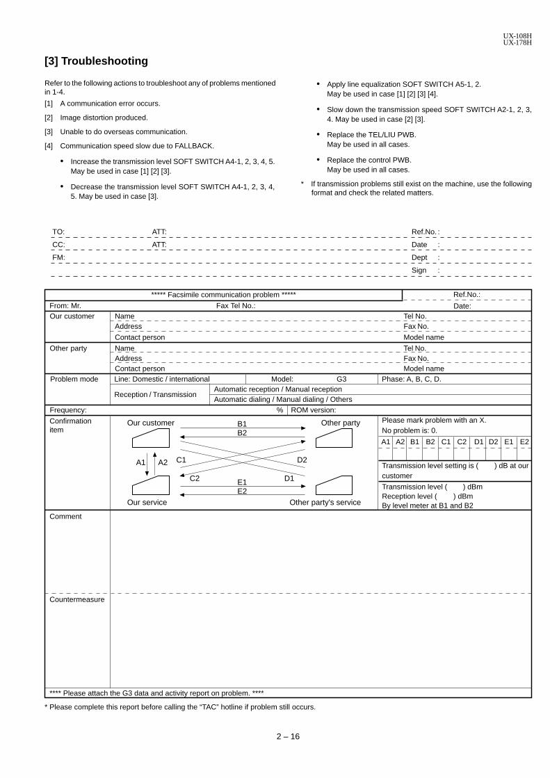
[3] Troubleshooting
Refer to the following actions to troubleshoot any of problems mentionedin 1-4.
[1] A communication error occurs.
[2] Image distortion produced.
[3] Unable to do overseas communication.
[4] Communication speed slow due to FALLBACK.
• Increase the transmission level SOFT SWITCH A4-1, 2, 3, 4, 5.May be used in case [1] [2] [3].
• Decrease the transmission level SOFT SWITCH A4-1, 2, 3, 4,5. May be used in case [3].
• Apply line equalization SOFT SWITCH A5-1, 2.May be used in case [1] [2] [3] [4].
• Slow down the transmission speed SOFT SWITCH A2-1, 2, 3,4. May be used in case [2] [3].
• Replace the TEL/LIU PWB.May be used in all cases.
• Replace the control PWB.May be used in all cases.
* If transmission problems still exist on the machine, use the followingformat and check the related matters.
TO: ATT: Ref.No. :
CC: ATT: Date :
FM: Dept :
Sign :
* Please complete this report before calling the “TAC” hotline if problem still occurs.
***** Facsimile communication problem ***** Ref.No.:
Date:From: Mr. Fax Tel No.:Our customer Name Tel No.
Address Fax No.
Contact person Model name
Other party Name Tel No.Address Fax No.Contact person Model name
Problem mode Line: Domestic / international Model: G3 Phase: A, B, C, D.
Reception / TransmissionAutomatic reception / Manual receptionAutomatic dialing / Manual dialing / Others
Frequency: % ROM version:
Confirmationitem
Please mark problem with an X.No problem is: 0.
A1 A2 B1 B2 C1 C2 D1 D2 E1 E2
Transmission level setting is ( ) dB at ourcustomer
Transmission level ( ) dBmReception level ( ) dBmBy level meter at B1 and B2
Comment
**** Please attach the G3 data and activity report on problem. ****
Countermeasure
Our customer
Our service
A1 A2 C1 D2
B1B2
E1E2
C2 D1
Other party
Other party's service

UX-108HUX-178H
2 – 17
[4] Error code table
1. Communication error code table
G3 TransmissionCode Final received signal Error Condition (Receiver side)
0 Incomplete signal frame Cannot recognize bit stream after flag
1 NSF, DIS Cannot recognize DCS signal by echo etc.
Cannot recognize NSS signal (FIF code etc)
2 CFR Disconnects line during reception (carrier missing etc)
3 FTT Disconnects line by fall back
4 MCF Disconnects line during reception of multi page
Cannot recognize NSS, DCS signal in the case of mode change
5 PIP or PIN The line is hung up without replying to telephone request from the receiving party.
6 RTN or RTP Cannot recognize NSS, DCS signal after transmit RTN or RTP signal.
7 No signal or DCN No response in receiver side or DCN signal received* (transmitter side)
8 − Owing to error in some page the error could not be corrected although the specified number of
error retransmission was at tempted.
11 − Error occurred after or while reception by the remote (receiving) machine was revealed to be
impossible.
12 − Error occurred just after fallback.
13 − Error occurred after a response to retransmission end command was received.
G3 Reception
Code Final received signal Error Condition (Receiver side)
0 Incomplete signal frame Cannot recognize bit stream after flag
1 NSS, DCS Cannot recognize CFR or FTT signal
Disconnects line during transmission (line error)
2 NSC, DTC Cannot recognize NSS signal (FIF code etc)
3 EOP Cannot recognize MCF, PIP, PIN, RTN, RTP signal
4 EOM Cannot recognize MCF, PIP, PIN, RTN, RTP signal in the case of mode change
5 MPS The line is hung up without replying to communication request.
6 PR1-Q Cannot recognize PIP, PIN signal in the case of TALK request
7 No signal or DCN No response in transmitter (cannot recognize DIS signal) or DCN signal received* (receiver side)
8 − Error occurred upon completion of reception of all pages.
9 − Error occurred when mode was changed or Transmission/Reception switching was performed.
10 − Error occurred during partial page or physical page reception.
11 − Error occurred after or during inquiry from the remote (transmitting) machine as to whether
reception is possible or not.
12 − Error occurred during or just after fallback.
13 − Error occurred after the retransmission end command was received.

UX-108HUX-178H
2 – 18
M E M O

UX-108HUX-178H
CHAPTER 3. MECHANISM BLOCKS
[1] General description
1. Document feed block and diagram
Fig. 1
2. Document feed operation1) The document placed in the hopper actuates the document sensor.
After one second, the pulse motor starts to drive the paper feed roller.The document is automatically taken up into the machine, and stoppedat the document sensor.
2) When a specified number of pulses are received from the documentsensor after the document lead edge is sensed, scanning is started.
3) When a specified number of pulses are received from the documentsensor after the document rear edge is sensed, scanning is termi-nated and the document is fed through.
4) If the document sensor is active (i.e., another document is in thehopper), when the preceding document scanning is completed and itis fed out, the next document is taken up into the machine. If thedocument sensor is not active (i.e., there is no document in the hop-per), when the document is fed out, the operation is terminated.
3. Hopper mechanism
3-1. General view
Fig. 2
The hopper is used to align documents with the document guides ad-justed to the paper width.NOTE: Adjust the document guide after setting up the document.
3-2. Automatic document feed1) Use of the paper feed roller and separation rubber plate ensures er-
ror-free transport and separation of documents. The plate springpresses the document to the paper feed roller to assure smooth feed-ing of the document.
2) Document separation method: Separation rubber plate
Fig. 3
3-3. Documents applicable for automatic feed
NOTE: Double-side coated documents and documents on facsimile re-cording paper should be inserted manually. The document feedquantity may be changed according to the document thickness.
Documents corresponding to a paper weight heavier than 64.3kg (74.3g/m2 ) and lighter than 135kg (157g/m2 ) are acceptable for manual feed.
Documents heavier than 135kg in terms of the paper weight must beduplicated on a copier to make it operative in the facsimile.
3-4. Loading the documents
1) Make sure that the documents are of suitable size and thickness, andfree from creases, folds, curls, wet glue, wet ink, clips, staples andpins.
2) Place documents face down in the hopper.
i) Adjust the document guides to the document size.
ii) Align the top edge of documents and gently place them into thehopper. The first page under the stack will be taken up by the feedroller to get ready for transmission.
NOTES: 1) Curled edge of documents, if any, must be straightenout.
2) Do not load the documents of different sizes and/orthicknesses together.
3 – 1
Paper size 1/2 Letter (148mm x 140mm) ~A4 (210mm x 297mm), Letter (216mm x 279mm)
4x6 series(788mm x 1091mm x1000mm sheets)
Squaremeter series
Minimum Maximum Minimum Maximum
Feeder capacity 10 sheets, max.
Paper thickness (ref.) 0.06mm 0.09mm 0.06mm 0.09mm
Paper weight 45kg 64.3kg 52g/m2 74.3g/m2
Fig. 4
Separator rubber
Rear roller A/B
Transfer roller
Pinch roller
CIS
Paper feed roller
Document
Paper feed spring
Separator rubber Paper feed spring
Document
Paper feed roller
Separator rubber Paper feed spring
Paper feed roller
Last page of document
First page of document
Back of document
UX-108HUX-178H
3-5. Documents requiring use of document carrier
1) Documents smaller than B6 (128mm x 182mm).
2) Documents thinner than the thickness of 0.06mm.
3) Documents containing creases, folds, or curls, especially those whosesurface is curled (maximum allowable curl is 5mm).
4) Documents containing tears.
5) Carbon-backed documents. (Insert a white sheet of paper betweenthe carbon back and the document carrier to avoid transfer of carbonto the carrier.)
6) Documents containing an easily separable writing material (e.g., thosewritten with a lead pencil).
7) Transparent documents.
8) Folded or glued documents.
Document in document carrier should be inserted manually into thefeeder.
4. Document release
4-1. GeneralWhen the release lever is pulled by hand in the direction of arrow, thelatch is released and the upper document guide moves on its axis in thederection of the arrow. The feed rollers, the separation rubber plate, andthe pinch rollers become free to make it possible to remove the docu-ment.
4-2. Cross section view
Fig. 5
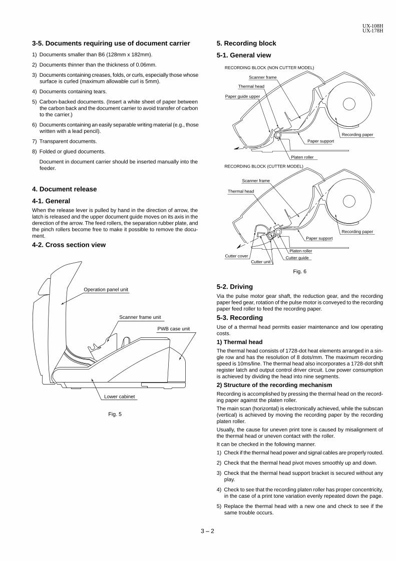
5. Recording block
5-1. General view
3 – 2
Operation panel unit
Scanner frame unit
PWB case unit
Lower cabinet
Fig. 6
5-2. DrivingVia the pulse motor gear shaft, the reduction gear, and the recordingpaper feed gear, rotation of the pulse motor is conveyed to the recordingpaper feed roller to feed the recording paper.
5-3. RecordingUse of a thermal head permits easier maintenance and low operatingcosts.
1) Thermal headThe thermal head consists of 1728-dot heat elements arranged in a sin-gle row and has the resolution of 8 dots/mm. The maximum recordingspeed is 10ms/line. The thermal head also incorporates a 1728-dot shiftregister latch and output control driver circuit. Low power consumptionis achieved by dividing the head into nine segments.
2) Structure of the recording mechanismRecording is accomplished by pressing the thermal head on the record-ing paper against the platen roller.
The main scan (horizontal) is electronically achieved, while the subscan(vertical) is achieved by moving the recording paper by the recordingplaten roller.
Usually, the cause for uneven print tone is caused by misalignment ofthe thermal head or uneven contact with the roller.
It can be checked in the following manner.
1) Check if the thermal head power and signal cables are properly routed.
2) Check that the thermal head pivot moves smoothly up and down.
3) Check that the thermal head support bracket is secured without anyplay.
4) Check to see that the recording platen roller has proper concentricity,in the case of a print tone variation evenly repeated down the page.
5) Replace the thermal head with a new one and check to see if thesame trouble occurs.
RECORDING BLOCK (CUTTER MODEL)
Scanner frame
Thermal head
Cutter coverPlaten roller
Paper support
Recording paper
Cutter guideCutter unit
RECORDING BLOCK (NON CUTTER MODEL)
Scanner frame
Thermal head
Paper guide upper
Platen roller
Paper support
Recording paper

UX-108HUX-178H
[2] Disassembly and assembly procedures
• This chapter mainly describes the disassembly procedures. For the assembly procedures, reverse the disassembly procedures.
• Easy and simple disassembly/assembly procedures of some parts and units are omitted. For disassembly and assembly of such parts and units,refer to the Parts List.
• The numbers in the illustration, the parts list and the flowchart in a same section are common to each other.
• To assure reliability of the product, the disassembly and the assembly procedures should be performed carefully and deliberately.
Handset cover and paper support guide1 Parts list (Fig. 1)
No. Part name Q’ty No. Part name Q’ty
1 Mechanism unit 1
2 Handset cover 1
3 Hook switch lever 1
4 Screw (ø3×12) 2
5 Paper support guide unit 1
6 Anti curl shaft 1
(Cutter model)
6 Guide wire 1
(Non cutter model)
7 Anti curl spring 2
(Cutter model)
Fig. 1
3 – 3
7 Guide wire sheet 1
(Non cutter model)
8 PO pinch roller 2
(Cutter model)
8 Paper set label 1
(Non cutter model)
9 Paper sensor lever 1
10 Paper sensor lever spring 1
11 Guide sheet 2
12 Sensor sheet 1
13 Paper support guide 1
9
106
3
2
2
3
4
5
6
7
4
4 1
55
1
8
78
7
13
1
8
9
10
11
12
Hook
Hook
Lock the all hook(4place)
11
1113
12 C U T T E RM O D E L
9
7
8
106
13
11
11
12
N O NC U T T E RM O D E L

UX-108HUX-178H
PWB case top, bottom and PWB2 Parts list (Fig. 2)
Fig. 2
3 – 4
No. Part name Q’ty No. Part name Q’ty
1 Mechanism unit 1
2 Screw (3×6) 1
3 Head earth cable 1
4 Connector 3
5 Screw (3×10) 1
6 PWB case unit 1
7 Screw (3×10) 2
8 PWB case, top 1
9 Screw (4×6) 1
10 AC cord ass’y 1
11 Screw (3×6) 1
12 TEL ARG cable 1
13 Power supply PWB unit 1
14 TEL/LIU PWB unit 1
15 Rubber leg 2
16 PWB case, bottom 1
2
3
4
5
6
1
6
13
10
1112
15
77
16
1
8
7
9
10
11
12
13
14
15
169
8
AC cordearth cable
45˚
2
5
3
4
Rib
3
ControlPWB
14
4

UX-108HUX-178H
Operation panel unit and scanner frame3 Parts list (Fig. 3)
Fig. 3
3 – 5
No. Part name Q’ty No. Part name Q’ty
1 Mechanism unit 1
2 Screw (3×10) 2
3 Scanner frame unit 1
4 Document guide lower 1
5 Reduction gear, 17/36Z 1
6 Reduction gear, 17/21Z 1
7 Idler gear, 25Z 1
8 Feed roller shaft 1
9 Feed roller 1
10 CIS cable 1
11 CIS support, right 1
12 CIS unit 1
13 CIS support, left 1
14 CIS spring 2
15 Scanner frame 1
16 Panel and head cable 2
17 Operation panel unit 1
2
3
4
516
17
1
7
6
8
9
10
11
14
15
12
13
8
4
15
98
5
6
147
10
14
11
2
232
3
116
16
17
1
1312
Stopper plate
Hook
Hook
Hook
2
3
1
11 13
Screwdriver
Mount the CIS unit by inserting a screw-driver between the scanner frame and CIS support and turning it (the same method on the left and right sides).
CIS support
,

UX-108HUX-178H
Document guide upper unit and headframe
4Parts list (Fig. 4)
Fig. 4
3 – 6
No. Part name Q’ty No. Part name Q’ty
1 Operation panel unit 1
2 Screw (3×10) 2
3 Support plate 1
4 Document guide upper 1
unit
5 Screw (3×10) 2
6 Head sheet 1
7 Head cable 1
8 Head spring A 2
9 Head spring B 3
10 Screw (3×6) 1
11 Head support, right 1
12 Screw (3×6) 1
13 Head earth cable 1
14 Head support, left 1
15 Thermal head 1
16 Pinch roller shaft 1
17 Pinch roller 2
18 Pinch roller pressing 2
spring
19 Head frame 1
1
4
2
162
1718
18
12
13
14
6
5
98
1011
15
53
19
87
13 14
B
A
View:A View:B
2
3
4
5
6
1
8
7
9
10
11
12
13
14
15
16
17
18
19

UX-108HUX-178H
Document guide upper5 Parts list (Fig. 5)
Fig. 5
3 – 7
No. Part name Q’ty No. Part name Q’ty
1 Rear sheet 1
2 CIS gear, 29Z 1
3 CIS roller A ass’y 1
4 Transfer bearing 1
5 Cuppling gear 1
6 CIS roller B ass’y 1
7 Transfer roller 1
8 Transfer bearing 1
9 Idler gear, 20Z 1
10 Panel lock lever spring 1
11 Panel lock lever 1
12 Document sensor lever 1
spring
13 Document sensor lever 1
14 Separate spring 1
15 Separator plate 1
16 Paper feed spring 1
17 Separator rubber 1
18 Document guide upper 1
2
1
3
4
5
6
8
7
9
10
11
12
13
14
15
16
17
Applying standard
Applying standard
13
12
15
14
14
17
16
13
12
10
9
18
17
82
4
3
6
1
11
18
5

UX-108HUX-178H
Operation panel6 Parts list (Fig. 6)
Fig. 6
3 – 8
No. Part name Q’ty No. Part name Q’ty
1 Operation panel unit 1
2 Screw (2×6) 3
3 Operation panel cable 1
4 Operation panel PWB 1
5 Document tray 1
6 Screw 1
7 Pinion gear 1
8 Hopper spring 1
9 Hopper guide, right 1
10 Hopper guide, left 1
11 Stop key 1
12 Start key 1
13 Direct key 1
14 12 key 1
15 Operation panel 1
Operation panel PWB LCD cable
LCD PWB
Confim of HOPPER GUIDE position
HOPPER GUIDE (R)
HOPPER GUIDE (L)
2
3
4
5
6
1
8
7
9
10 11
12
13
14
15 15
1
10
9
8
67
5
11
1213
14
22
3
2
4
1
RibRibGAP 0
GAP 0

UX-108HUX-178H
Parts list (Fig. 7)
Fig. 7
Drive unit, PWB and cutter7
3 – 9
No. Part name Q’ty No. Part name Q’ty
1 Mechanism unit 1
2 Screw (3×10) 2
(Cutter model)
2 Screw (3×10) 1
(Non cutter model)
3 Cutter arm 1
(Cutter model only)
4 Drive unit 1
5 Platen gear 1
6 Platen roller 1
7 Platen bearing 2
8 Screw (3×10) 1
(Cutter model only)
9 Cutter unit 1
(Cutter model only)
10 Screw (3×10) 1
(Cutter model only)
11 Cutter cover 1
(Cutter model only)
12 Cutter guide 1
(Cutter model only)
13 Cutter 1
(Cutter model only)
14 Screw (3×10) 2
15 Speaker cable 1
16 Control PWB unit 12
3
4
5
16
1
7
6
8
9
10
11
14
15
12
13
1
5
7
6
1
2 2
4
2 4
215
14
1416
6
16
7
35
78
9
10
1112
13
1
4
1
4
OK NGCuttermodelonly

UX-108HUX-178H
1 Mechanism unit 1
2 Paper sensor lever spring 1
(Cutter model only)
3 Paper sensor lever (Cutter model only) 1
4 Screw 2
5 Speaker 1
6 Paper guide upper (Non cutter model only) 1
Parts list (Fig. 8)
No. Part name Q’ty
Fig. 8
Speaker, paper sensor lever and paperguide upper8
3 – 10
2
3
4
5
1
1
2
3 4 4
5
6
1
1
5
1
6
2
3
RibHook
Hook
6

UX-108HUX-178H
Drive frame (Non cutter model)9
Fig. 9
3 – 11
Parts list (Fig. 9)
No. Part name Q’ty No. Part name Q’ty
1 Change lever spring 1
2 Planet gear, 17Z 1
3 Change lever A 1
4 Cam 1
5 Reduction gear, 17/36Z 1
6 Planet gear, 17Z 1
7 Planet gear spring 1
8 Planet gear lever A 1
9 Planet gear, 17Z 1
10 Planet gear spring 1
11 Planet gear lever B 1
12 Idler gear, 25Z 1
13 Cam switch 1
14 Reduction gear, 17Z 1
15 Idler gear, 25Z 1
16 Screw (3×10) 1
17 Motor 1
18 Motor heat sink 1
19 Drive frame 1
1
2
3
4
5
6
9
19
7
10
8
11
13
12
14
15
16
17
18
1619 13
17 18
1913
146
7
8
11
9
1015
412
2
1
1
3
3
5
107
To be the switchlinked by hooks
Grease
Grease
Green
Lock the MOTORby this rib
SECTION : A-A
A
A
Hook be doing lock
NOTE) Apply certainly to a part of a nail at the time of GREASE application
GEAR attachment boss
,
96 ,

UX-108HUX-178H
Drive frame (Cutter model)10
Fig. 10
Parts list (Fig. 10)
No. Part name Q’ty No. Part name Q’ty No. Part name Q’ty
1 Cutter cam switch 1
2 Planet gear, 17Z 1
3 Planet gear spring 1
4 Planet gear lever C 1
5 Change lever spring 1
6 Planet gear, 17Z 1
7 Change lever A 1
8 Cam 1
9 Reduction gear, 17/36Z 1
10 Cutter gear, 44Z 1
11 Planet gear, 17Z 1
12 Planet gear spring 1
13 Planet gear lever A 1
14 Planet gear, 17Z 1
15 Planet gear spring 1
16 Planet gear lever B 1
17 Idler gear, 25Z 1
18 Cam switch 1
19 Reduction gear, 17/30Z 1
20 Reduction gear, 17/30Z 1
21 Reduction gear, 17/36Z 1
22 Idler gear, 25Z 1
23 Idler gear, 25Z 1
24 Idler gear, 20Z 1
25 Screw (3×10) 1
26 Motor 1
27 Motor heat sink 1
28 Drive frame 1
3 – 12
1
2
5
8
9
10
11
14
3
6
12
15
4
7
13
16
18
17
19
20
21
22
23
24
25
26
27
28
25
28 1 18
26 27
1
2818
2111
12
13
16
14
15
24
23
817
6
5
5
7
742
3
20
19
922
12 15
10
3
To be the switchlinked by hooks
WHITE
GREEN
Lock the MOTORby this rib
SECTION : A-A
A
A
Hook be doing lock
, ,
,Grease
Grease
1411 ,
NOTE) Apply certanly to a part of a nail at the time of GREASE application
GEAR attachment boss

UX-108HUX-178H
3 – 13
Fig. 9
Wire treatment11 Parts list (Fig. 10)
1 Band 5
2 Screw (3×6) 2
3 Screw (4×6) 1
4 UL tape 1
5 Core (F2064) 1
6 Core (F2063) 1
7 Band (100mm) 1
No. Part name Q’ty
23
Rib Power supplyPWB
TEL/LIUPWB
AC cord
ARGcable
OK NG
Head earth cable
Camswitchcable
Camswitchcable
11
7
7
100 10mm
20 5mm
Head, head earth and panel cable
Head cable
Motor cable
Binding the cable(Head cable/Head earth cable/CIS cable/panel cable/motor cable/cam switch cable)
Head cable and headearth cable
Head earth cable
Head cable
Operation panel PWB
Panel cable
Panel cable
CIScable
CIScable
CIS unit
1
6
1
65
1
1
5
Postion of core
Panel cableHead earth cable pass tounder the core 1 time
All the cable must wiring to under the motor heat sink
Binding the core with lower cabinet
Binding the core with head and panel cable
0~2mm
19mmPanel cable 4
CIS cable passto the core 2 times
2
Rib
Speaker
Speaker cable
Control PWB
Headearthcable
1
Head cable and panel cablepass to the core 2 times
Fixed this switch after adjusting the cutter gear in this drawing,(Cutter model only)
Cutter cable

UX-108HUX-178H
4 – 1
[1] B
lock
dia
gram
CHAPTER 4. DIAGRAMS
MO
DE
M
CLO
CK
SR
AM
25
6Kbi
tR
OM
1M
bit
CP
U
CP
U I/
F
TIM
ER
RT
C
PIO
WA
TC
HD
OG
T
IME
R
CLO
CK
32
kHz
INT
ER
RU
PT
C
ON
TR
OLL
ER
CIS
I/F
MO
TO
R I/
F
SE
NS
OR
I/F
SIO
TH
ER
MA
L H
EA
D I/
F
PA
NE
L I/F
PM
OP
ER
AT
ION
P
AN
EL
LCD
CO
NT
RO
L P
WB
UN
IT1C
HIP
FA
X E
NG
INE
(X
FC
-3)
HA
ND
SE
T
SP
EA
KE
R
+5V
+24
V
OP
ER
AT
ION
P
AN
EL
TE
L/LI
U
PW
B U
NIT
DR
IVE
R
TH
ER
MA
L H
EA
D
PM
CO
NT
AC
T
IMA
GE
SE
NS
OR
DO
CU
ME
NT
SE
NS
OR
PO
WE
R S
UP
PLY
P
WB
UN
IT
PA
PE
R S
EN
SO
R A
ND
CU
TT
ER
: U
X-1
78H
ON
LY
AM
P/S
IGN
AL
SE
LEC
T
B
LOC
K
SP
EA
KE
R
AM
P
AM
P
AM
P
SU
RG
E
PR
OT
EC
T/
FIL
TE
RC
ML
TR
AN
S
CI
VB
T
RE
GU
LAT
OR
RE
CT
IFIE
R
TR
AN
S
RE
CT
IFIE
R
DIO
DE
TR
AN
SS
UR
GE
A
BS
OR
BE
RF
ILT
ER
ST
AB
ILIZ
ER
LIN
E
EX
T.T
EL
PA
PE
R
SE
NS
OR
RE
SE
T IC
24M
Hz
12M
Hz
CU
TT
ER
AM
P
BZ

UX-108HUX-178H
[2] W
iring
dia
gram
4 – 2
FG
CN
LIU
BC
NLI
UB
6
CA
M S
W
CU
TT
ER
S
EN
SO
R
22
6
TH
ER
MA
L H
EA
D
CO
NT
AC
T IM
AG
E S
EN
SO
R
LCD
UN
IT
CN
LCD
OP
ER
AT
ION
P
AN
EL
PW
B
14
CN
PN
16 7 15
CN
CS
WC
NM
T
CN
TH
CN
CIS
CN
PN
CN
SP
SP
EA
KE
R
CN
CU
T1
CN
LIU
A
CN
PW
10 10
CO
NT
RO
L P
WB
UN
IT
TE
L/LI
U
PW
B U
NIT
PO
WE
R S
UP
PLY
P
WB
UN
IT
CN
LIU
A
CN
2
EX
TE
RN
AL
LIN
E
TE
L LI
NE
MJ1
/2
MJT
EL
AC
CO
RD
UX
-178
H O
NLY
TX
/RX
MO
TO
R
2
HA
ND
SE
T
FG

UX-108HUX-178H
[3] P
oint
- to
-poi
nt d
iagr
am
4 – 3
TX
/RX
MO
TO
R
TP
AD
TP
BD
TP
AD
TP
BD
VM
TV
MT
1 2 3 4 5 6 1 2 3 4 5 6 7 8 9 10 11 12 13 14 15 16
1 2 3 4 5 6 7 8 9 10 11 12 13 14 15 16
1 2 3 4 5 6 7 8 9 10 11 12 13 14 15
1 2 3 4 5 6 7 8 9 10 11 12 13 14 151 2 3 4 5 6
OP
ER
AT
ION
PA
NE
LP
WB
TP
AD
TP
BD
TP
AD
TP
BD
VM
TV
MT
TH
ER
MA
LH
EA
D
VT
HV
TH
ST
RB
1S
TR
B2
TH
IR
AN
KM
GM
GM
G+
5VS
TR
B3
ST
RB
4LA
TC
HP
CLK
DA
TA
VT
H
VT
HV
TH
ST
RB
1S
TR
B2
TH
IR
AN
KM
GM
GM
G+
5VS
TR
B3
ST
RB
4LA
TC
HP
CLK
DA
TA
VT
H
1 2 3 4 5 6 7
1 2 3 4 5 6 7
VO
DG
+5V øT
CIS
CLK
GLE
D+
24V
VO
DG
+5V øT
CIS
CLK
GLE
D+
24V
KE
N4A
KE
N3A
KE
N2A
KE
N1A
DG
DG
+5V
OR
GS
NS
FR
SN
SE
SE
N4
SE
N3
SE
N2
SE
N1
SE
N0
KE
N4A
KE
N3A
KE
N2A
KE
N1A
DG
DG
+5V
OR
GS
NS
FR
SN
SE
SE
N4
SE
N3
SE
N2
SE
N1
SE
N0
CN
PN
CN
PN
CN
CIS
1 2 3 4 5 6 7 8 9 10
1 2 3 4 5 6 7 8 9 10
TE
L/LI
UP
WB
TE
LMU
TE
CI
HS
RH
SR
XIN
TX
OU
TC
ML
+24
VA
+5V DG
TE
LMU
TE
CI
HS
RH
SR
XIN
TX
OU
TC
ML
+24
VA
+5V DG
CN
LIU
AC
NLI
UA
CN
MT
CN
TH
1 2 3 4 5 6 7 8 9 10
1 2 3 4 5 6 7 8 9 10
PO
WE
RS
UP
PLY
PW
B
DG
+5V
VT
HO
NM
GM
GM
G+
24V
VT
HV
TH
VT
H
DG
+5V
VT
HO
NM
GM
GM
G+
24V
VT
HV
TH
VT
H
CN
2C
NP
W
CN
CS
W
CN
SP
CIS
1 2C
SW
DG
CA
MS
WIT
CH
1 2
1 2 1 2S
P+
SP
-
CS
WD
G
SP
+S
P-
SP
EA
KE
R
CO
NT
RO
LP
WB
1 2 3 4 5 6
1 2 3 4 5 6
EX
TS
IGN
.C.
RX
MU
TE
DP
ON
DP
MU
TE
E-R
LY
EX
TS
IGN
.C.
RX
MU
TE
DP
ON
DP
MU
TE
E-R
LY
CN
LIU
BC
NLI
UB
CN
CU
T1
1 2C
UT
1D
GC
UT
TE
RS
WIT
CH
1 2C
UT
1D
G
(UX
-178
H O
NLY
)
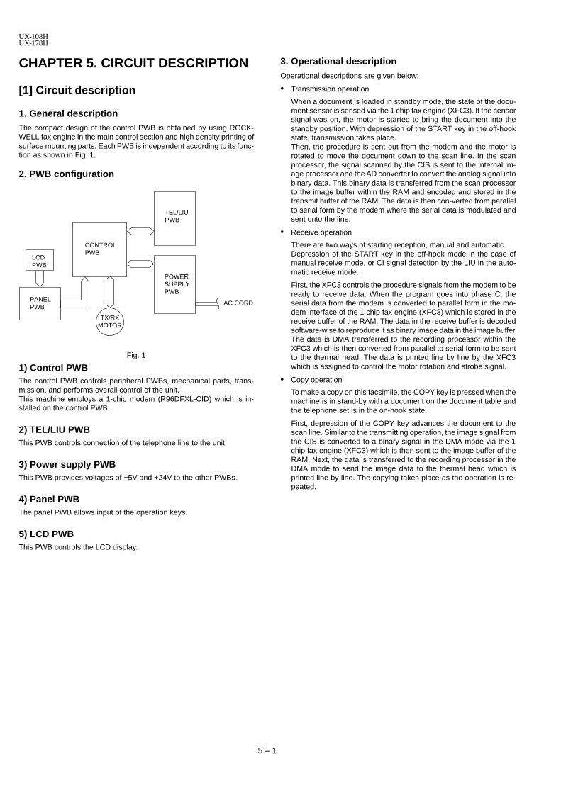
UX-108HUX-178H
CHAPTER 5. CIRCUIT DESCRIPTION
[1] Circuit description
1. General descriptionThe compact design of the control PWB is obtained by using ROCK-WELL fax engine in the main control section and high density printing ofsurface mounting parts. Each PWB is independent according to its func-tion as shown in Fig. 1.
2. PWB configuration
Fig. 1
1) Control PWBThe control PWB controls peripheral PWBs, mechanical parts, trans-mission, and performs overall control of the unit.This machine employs a 1-chip modem (R96DFXL-CID) which is in-stalled on the control PWB.
2) TEL/LIU PWBThis PWB controls connection of the telephone line to the unit.
3) Power supply PWBThis PWB provides voltages of +5V and +24V to the other PWBs.
4) Panel PWBThe panel PWB allows input of the operation keys.
5) LCD PWBThis PWB controls the LCD display.
3. Operational descriptionOperational descriptions are given below:
• Transmission operation
When a document is loaded in standby mode, the state of the docu-ment sensor is sensed via the 1 chip fax engine (XFC3). If the sensorsignal was on, the motor is started to bring the document into thestandby position. With depression of the START key in the off-hookstate, transmission takes place.Then, the procedure is sent out from the modem and the motor isrotated to move the document down to the scan line. In the scanprocessor, the signal scanned by the CIS is sent to the internal im-age processor and the AD converter to convert the analog signal intobinary data. This binary data is transferred from the scan processorto the image buffer within the RAM and encoded and stored in thetransmit buffer of the RAM. The data is then con-verted from parallelto serial form by the modem where the serial data is modulated andsent onto the line.
• Receive operation
There are two ways of starting reception, manual and automatic.Depression of the START key in the off-hook mode in the case ofmanual receive mode, or CI signal detection by the LIU in the auto-matic receive mode.
First, the XFC3 controls the procedure signals from the modem to beready to receive data. When the program goes into phase C, theserial data from the modem is converted to parallel form in the mo-dem interface of the 1 chip fax engine (XFC3) which is stored in thereceive buffer of the RAM. The data in the receive buffer is decodedsoftware-wise to reproduce it as binary image data in the image buffer.The data is DMA transferred to the recording processor within theXFC3 which is then converted from parallel to serial form to be sentto the thermal head. The data is printed line by line by the XFC3which is assigned to control the motor rotation and strobe signal.
• Copy operation
To make a copy on this facsimile, the COPY key is pressed when themachine is in stand-by with a document on the document table andthe telephone set is in the on-hook state.
First, depression of the COPY key advances the document to thescan line. Similar to the transmitting operation, the image signal fromthe CIS is converted to a binary signal in the DMA mode via the 1chip fax engine (XFC3) which is then sent to the image buffer of theRAM. Next, the data is transferred to the recording processor in theDMA mode to send the image data to the thermal head which isprinted line by line. The copying takes place as the operation is re-peated.
5 – 1
LCDPWB
PANELPWB
CONTROLPWB
TEL/LIUPWB
POWERSUPPLYPWB
TX/RXMOTOR
AC CORD

UX-108HUX-178H
[2] Circuit description of control PWB
1. General descriptionFig. 2 shows the functional blocks of the control PWB, which is com-posed of 4 blocks.
Fig. 2 Control PWB functional block diagram
2. Description of each block
(1) Main control blockThe main control block is composed of ROCKWELL 1 chip fax engine(XFC3), ROM (128KByte), RAM (32KByte) and Modem (R96DFXL-CID).Devices are connected to the bus to control the whole unit.
1) XFC3 (IC2) : pin-144 QFP (XFC3)
2) R96DFXL-CID (IC4) : pin-100 QFP (MODEM)The FAXENGINE Integrated Facsimile Controllers.
XFC3, contains an internal 8 bit microprocessor with an external 2 Mbyteaddress space and dedicated circuitry optimized for facsimile imageprocessing and facsimile machine control and monitoring.
3) 27C01012 (IC7): pin-32 DIP (ROM)EPROM of 1Mbit equipped with software for the main CPU.
3) W24257S-70LL (IC5): pin-28 SOP (RAM)Line memory for the main CPU system RAM area and coding/decodingprocess. Used as the transmission buffer.
Memory of recorded data such as daily report and auto dials. When thepower is turned off, this memory is backed up by the lithium battery.
Fig. 3
MC24 CPU CONTROL IF
MC24 MEGACELL(8BIT DATA,24BIT ADDRESS) WATCHDOG TIMER REAL TIME CLOCK
CRYSTAL OSCILLATOR BATTERY BACK-UP CIRCUIT INTERRUPT CONTROLLER
BUS INTERFACE
DRAM CONTROL INTERNAL & EXTERNAL BUS CONTROL
INTERNAL & EXTERNAL DECODE DMA CONTROLLER OPERATOR PANEL IF
32 KEYS 8 LEDS
LCD MODULE SYNC SERIF 1
THERMAL PRINTER IF
5 ms LINE TIME A4/B4 LINES
TPH ADC 4 STROBE TPH
LATCHLESS TPH EXTEMAL DMA I/F
T.4/T.6 CODEC
MH,MR,MMR HARDWARE,ALTERNATE
COMPRESSION & DECOMPRESSION
BI-LEVEL RESOLUTION CONVERSION
PROGRAMMABLE
REDUCTION & EXPANSION
2.6kBYTE VIDEO RAM
SCANNER CONTROL & VIDEO PROCESSING 8-BIT PADC
CCD/CIS SCANNER 5 ms,A4/B4 LINES
SHADING CORRECTION(1:1,1:8) DITHERING
MULTILEVEL B4-A4 REDUCTION ERROR DIFFUSION
MTF
GENERAL I/O TONE/MODTONE
GPIO AUTOBAUD
SYNC-ASYNC SASIF SYNC SERIF 2
FLASH MEMORY IF AUTOBAUD
CPU BUS
INTERNAL CPU BUS
EXTERNAL CPU BUS
DMA BUS
WRPROTN
TSTCLKDEBUGNRESETNXINXOUTPWRDWNNBATRSTN
SYSCLK
SEE "OPIF OUTPUTS" BELOW
SEE "OPIF INPUTS" BELOW
THADIN
PDATPLATSTRB[3:0]STRBPOL
PCLK
PWR/GND TEST OPIF INPUTS OPI[0]/GPIO[21]/SSRXD1 OPI[1]/GPIO[22]/SSSTAT1 OPI[2]/GPIO[23]/SSCLK1 OPI[3]/GPIO[24]
OPIF OUTPUTS LEDCTL/GPO[16] LCDCS/GPO[17] OPO[0]/GPO[8] OPO[1]/GPO[9] OPO[2]/GPO[10] OPO[3]/GPO[11] OPO[4]/GPO[12]/SSTXD1 OPO[5]/GPO[13] OPO[6]/GPO[14] OPO[7]/GPO[15]
ROMCSN
MCSNSYNC
REGDMAWAITNRASN
CASN[1:0]DWRN
CSN[1:0]
WRNRDN
D[7:0]A[23:0]MIRQN
TONE
VINCLK1CLK1N
CLK2VIDCTL0/FCS1NVIDCTL1/FCS2N
START –VREF+VREF
GPIO[0] GPIO[1]/SASTXD GPIO[2]/SASRXD GPIO[3]/SASCLK GPIO[4] GPIO[5]/SSCLK2 GPIO[6]/SSTXD2 GPIO[7]/SSRXD2 GPIO[8]/FWRN GPIO[9]/FRDN GPIO[10]/SSSTAT2 GPIO[11]/BE/SERINP GPIO[12]/CS2N GPIO[13]/CS3N GPIO[14]/CS4N GPIO[15]/CS5N GPIO[16]/IRQ8 GPIO[17]/IRQ5N GPIO[18]/IRQ9N GPIO[19]/RDY/SEROUT GPIO[20]/ALTTONE SM[3:0]/GPO[7:4] PM[3:0]/GPO[3:0]
5 – 2
XFC3
ROM
MODEM
RAM
(1)
(2)
(4)
(3)
MAIN CONTROL BLOCK
MODEM BLOCK

UX-108HUX-178H
XFC3 (IC2) Terminal descriptions
CPU Control InterfaceMIRQn 135 I HU − Modem interrupt, active low. (Hysteresis In, Internal Pullup.)SYSCLK 133 I H − System clock. (Hysteresis In.)TSTCLK 130 O − 123XT Test clock.
Bus Control InterfaceA[23:0] [1:6][8:13] O TU 123XT Address bus (24-bit).
[15:20][22:27]D[7:0] [136:139] I/O TU 123XT Data bus (8-bit).
[141:144]RDn 128 O − 123XT Read strobe.WRn 127 O − 123XT Write strobe.ROMCSn 120 O − 123XT ROM chip select.CS1n 122 O − 123XT I/O chip select.CS0n 57 O − 123XT SRAM chip select. (Battery powered.)MCSn 121 O − 123XT Modem chip select.SYNC 126 O − 123XT Indicates CPU op code fetch cycle (active high).REGDMA 124 O − 123XT Indicates REGSEL cycle and DMA cycle.WAITn 125 O − 123XT Indicates current TSTCLK cycle is a wait state or a halt state.RASn 113 O − 123XT DRAM row address select. (Battery powered.)CAS[1:0]n [111:112] O − 123XT DRAM column address select. (Battery powered.)DWRn 109 O − 123XT DRAM write. (Battery powered.)
Prime Power Reset Logic and TestDEBUGn 129 I HU − External non-maskable input (NMI).RESETn 131 I/O HU 2XO XFC3 Reset.TEST 58 I C − Sets Test mode (Battery powered).
Battery Power Control and Reset LogicXIN 59 I OSC − Crystal oscillator input pin.XOUT 60 O − OSC Crystal oscillator output pin.PWRDWNn 62 I H − Used by external system to indicate loss of power to XFC3. (Results in NMI)BATRSTn 61 I H − Battery power reset input.WRPROTn 110 O − 1XC (Battery powered.) Write protect during loss of VDD power.
Scanner InterfaceSTART 101 O − 2XS Scanner shift gate control.CLK1 100 O − 2XS Scanner clock.CLK1n 99 O − 2XS Scanner clock-inverted.CLK2 98 O − 2XS Scanner reset gate control (or clock for CIS scanner).FCS1n/VIDCTL0 96 O − 2XT Flash memory chip select or Video Control signal.FCS2n/VIDCTL1 97 O − 2XT Flash memory chip select or Video Control signal.
Printer InterfacePCLK 29 O − 3XC Thermal Print Head (TPH) clock, or external DMAACK.PDAT 30 O − 2XP Serial printing data (to TPH).PLAT 31 O − 3XP TPH data latch.STRB[3:0] [33:36] O − 1XP Strobe signals for the TPH.STRBPOL 37 I C − Sets strobe polarity, active high/low.
Operator Panel InterfaceOPO[0]/GPO[8]/ 47 O − 2XL Keyboard/LED strobe [0] or GPO[8] or Scan Motor Power ControlSMPWRCTRLOPO[1]/GPO[9]/ 46 O − 2XL Keyboard/LED strobe [1] or GPO[9] or Print Motor Power ControlPMPWRCTRLOPO[2]/GPO[10]/ 44 O − 2XCT Keyboard/LED strobe [2] or GPO[10] or RINGERRINGEROPO[3]/GPO[11] 43 O − 2XL Keyboard/LED strobe [3] or GPO[11]OPO[4]/GPO[12]/ 42 O − 2XL Keyboard/LED strobe [4] or GPO[12] or SSTXD1 (for SSIF1)SSTXD1OPO[5]/GPO[13] 40 O − 2XL Keyboard/LED strobe [5] or GPO[13]OPO[6]/GPO[14] 39 O − 2XL Keyboard/LED strobe [6] or GPO[14]OPO[7]/GPO[15] 38 O − 2XL Keyboard/LED strobe [7] or GPO[15]OPI[0]/GPIO[21]/ 52 I/O HU 2XC (Pullup, Hysteresis In) Keyboard return [0] or GPIO[21] or SSRXD1SSRXD1 (for SSIF1)OPI[1]/GPIO[22]/ 51 I/O HU 2XC (Pullup, Hysteresis In) Keyboard return [1] or GPIO[22] or SSSTAT1SSSTAT1 (for SSIF1)OPI[2]/GPIO[23]/ 50 I/O HU 2XC (Pullup, Hysteresis In) Keyboard return [2] or GPIO[23] or SSCLK1SSCLK1 (for SSIF1)
Pin Name Pin No. I/OInput Output Pin Description
Type Type (Note: Active low signals have an "n" pin name ending.)
5 – 3

UX-108HUX-178H
XFC3 (IC2) Terminal descriptions
Operator Panel InterfaceOPI[3]/GPIO[24] 49 I/O HU 2XC (Pullup, Hysteresis In) Keyboard return [3] or GPIO[24]LEDCTL 55 O − 4XC Indicates outputs OPO[7:0] are for LEDs.LCDCS 54 O − 1XC LCD chip select.
General Purpose I/OGPIO[0] 94 I/O H 2XC (Hysteresis In) GPIO[0].GPIO[1]/SASTXD 93 I/O H 2XC (Hysteresis In) GPIO[1] or SASTXD (for SERIF).GPIO[2]/SASRXD 92 I/O H 2XC (Hysteresis In) GPIO[2] or SASRXD (for SERIF).GPIO[3]/SASCLK 91 I/O H 2XC (Hysteresis In) GPIO[3] or SASCLK (for SERIF).GPIO[4]/CPCIN 90 I/O H 2XC (Hysteresis In) GPIO[4] or Calling Party Control Input.GPIO[5]/SSCLK2 89 I/O H 2XC (Hysteresis In) GPIO[5] or SSCLK2 (for SSIF2).GPIO[6]/SSTXD2 87 I/O H 2XC (Hysteresis In) GPIO[6] or SSTXD2 (for SSIF2).GPIO[7]/SSRXD2 86 I/O H 2XC (Hysteresis In) GPIO[7] or SSRXD2 (for SSIF2).GPIO[8]/FWRn 85 I/O H 2XC (Hysteresis In) GPIO[8] or flash write enable signal for NAND-type flash
memory.GPIO[9]/FRDn 84 I/O H 2XC (Hysteresis In) GPIO[9] or flash read enable signal for NAND-type flash
memory.GPIO[10]/SSSTAT2 83 I/O H 2XC (Hysteresis In) GPIO[10] or SSSTAT2 (for SSIF2).GPIO[11]/BE/ 82 I/O H 1XC (Hysteresis In) GPIO[11] or bus enable or serial port data input forSERINP autobaud detection.GPIO[12]/CS[2]n 80 I/O H 2XC (Hysteresis In) GPIO[12] or I/O chip select [2].GPIO[13]/CS[3]n 79 I/O H 2XC (Hysteresis In) GPIO[13] or I/O chip select [3].GPIO[14]/CS[4]n 78 I/O H 2XC (Hysteresis In) GPIO[14] or I/O chip select [4].GPIO[15]/CS[5]n 77 I/O H 2XC (Hysteresis In) GPIO[15] or I/O chip select [5].GPIO[16]/IRQ[8] 76 I/O H 1XC (Hysteresis In) GPIO[16] or external interrupt 8.GPIO[17]/IRQ[5]n 75 I/O H 1XC (Hysteresis In) GPIO[17] or external interrupt 5.GPIO[18]/IRQ[9]n 74 I/O H 1XC (Hysteresis In) GPIO[18] or external interrupt 9.GPIO[19]/RDY/ 73 I/O H 1XC (Hysteresis In) GPIO[19] or ready signal or Serial port data output forSEROUT autobaud detection.GPIO[20]/ALTTONE 107 I/O H 1XC (Hysteresis In) GPIO[20] or ALTTONE.
MiscellaneousSM[3:0]/GPO[7:4] [103:106] O − 1XC Programmable: scan motor control pins or GPO pins.PM[3:0]/GPO[3:0] [115:118] O − 1XC Programmable: print motor control pins or GPO pins.TONE 119 O − 1XC Tone output signal.
Power, Reference Voltages, Ground-Vref/CLREF 66 I -VR − Negative Reference Voltage for Video A/D or Reference Voltage for the
Clamp Circuit.ADXG 68 I VXG − A/D Internal GND. (NOTE: This pin requires an external 0.22µF decoupling
capacitor to ADGA.)ADGA 69 VADG A/D Analog GroundADVA 70 VADV A/D Analog PowerADGD 72 VADG A/D Digital Ground+Vref 71 I +VR Positive Reference Voltage for Video A/D.VIN 67 I VA − Analog Video A/D input.THADI 65 I TA − Analog Thermal A/D input.
Power and GroundVSS(12) 7,21,28,45, Digital Ground
53,56,64,88,95,108,132,134
VDD(8) 14,32,41,48, Digital Power81,102,123,140
VBAT 63 Battery PowerVDRAM 114 DRAM Battery Power
Pin Name Pin No. I/OInput Output
Pin DescriptionType Type
5 – 4

UX-108HUX-178H
(2) Panel control blockThe following controls are performed by the XFC3.
• Operation panel key scanning
• Operation panel LCD display
(3) Mechanism/recording control block
• Recording control block diagram (1)
Fig. 4
OPERATOR PANEL,
KEYPAD, LEDS & LCD
PANEL/LCD PWB
PRINTER DATA CONTROI & SENSORS
THERMAL HEAD
OPO[7:0]*OPI[3:0]*LEDCTL*LCDCS*
TESTBATRSTNRESETN
STRB[3:0]STRBPOLTHADIPDATPCLKPLAT
TONE/ALTTONETSTCLKREGDMAWAITNSYNCPWRDWNN
PRINTER & SCANNER
MOTOR DRIVERS
MOTORPM[3:0]*
SM[3:0]*
RTC CRYSTAL
SCANNER CONTROLS &
SENSORS
STARTCLK2CLK1CLK1NVIDCTL[1:0]
XINXOUT
MIRONMCSN
SYSCLK
D[7:0]RDN
A[4:0]
WRN
MONOFAX FACSIMILE
MODEM
ANALOG SWITCH
LINE INTERFACE
SPEAKER MICROPHONE
CIRCUIT
TELEPHONE LINE
RX
AT
XA SP
KR
MIC
RIN
SP
KR
LOS
PK
RH
I
SPKRRIN
TX
A2
TX
A1
TXOUTRXIN
XIA
GPIO
DRAM (OPTION)
SCANNER VIDEO
PREPROCESSING
SYNC PORTS (2) (SSIF)
VIN+VREF
–VREF
SSCLK[2:1]*SSTXD[2:1]*SSRXD[2:1]*SSSTAT[2:1]*
SYNC/ASYNC SERIAL PORT
SASCLKSASTXD
SASRXD
GPIOGENERAL PURPOSE I/O
CIS
DEBUGNVDDVDRAMVBATVSS
FLASH MEMORY
WRPROTNFRDN*FRWN*FCLE*FCS[0:2]
D[7:0]RDN
A[23:0]
WRNROMSCN
CS[5:0]N*
TXDATRMODE
RXDAT
TMODECLKINSLEEPN
GPIO
CAS[0,1]N,RASN,DWRN
NOTES:*ALTERNATIVE GPO,GPI OR GPIO LINES
SPEAKERPHONE ONLY
VOICE OR SPEAKERPHONE
EXTENDED FACSIMILE
CONTROLLER XFC-(M)
EX
TE
RN
AL B
US
5 – 5

UX-108HUX-178H
(4) Modem (R96DFXL-CID) block
INTRODUCTIONThe Rockwell R96DFXL-CID MONOFAX modem is a synchronous 9600bits per second (bps) half-duplex modem with error detection and DTMFreception. It has low power consumption and requires only a single +5VDC power supply. The modem is housed in a single VLSI device pack-age.The modem can operate over the public switched telephone network(PSTN) through line terminations provided by a data access arrange-ment (DAA).The R96DFXL-CID is designed for use in Group 3 facsimile ma-chines.The modem satisfies the requirements specified in CCITT recommen-dations V.29, V.27 ter, V.21 Channel 2 and T.4, and meets the binarysignaling requirements of T.30.The modem can operate at 9600, 7200, 4800, 2400, or 300 bps, andalso includes the V.27 ter short training sequence option.The modem can also perform HDLC framing according to T.30 at 9600,7200, 4800, 2400, or 300 bps.The modem features a programmable DTMF receiver and three pro-grammable tone detectors which operate concurrently with the V.21channel 2 receiver.The voice mode allows the host computer to efficiently transmit andreceive audio signals and messages.The modem is available in either a 100-pin plastic quad flat pack (PQFP)or a 64-pin quad in-line package (QUIP).General purpose input/output (GPIO) pins are available for host assignment in the 100-pin PQFP.The modem’s small size, single voltage supply, and low power con-sumption allow the design of compact system enclosures for use in bothoffice and home environments.MONOFAX is a registered trademark of Rockwell International.
FEATURES
• Group 3 facsimile transmission/reception
– ITU-TS V.29, V.27 ter, T.30, V.21 Channel 2, T.4
– HDLC Framing at all speeds
• V.27 ter short train
• Concurrent DTMF, FSK, and tone reception
• Voice mode transmission/reception
• Half-duplex (2-wire)
• Programmable maximum transmit level:
0 dBm to –15 dBm
• Programmable transmit analog attenuation:
0 dB to 14 dB in 2 dB steps
• Receive dynamic range: 0 dBm to –43 dBm
• Programmable dual tone generation
• Programmable tone detection
• Programmable turn-on and turn-off thresholds
• Programmable interface memory interrupt
• Diagnostic capability
– Allows telephone line quality monitoring
• Equalization
– Automatic adaptive equalizer
– Fixed digital compromise equalizer
• DTE interface: two alternate ports
– Selectable microprocessor bus (6500 or 8085)
– CCITT V.24 (EIA-232-D compatible) interface
• TTL and CMOS compatible
• Low power consumption: 275 mW (typical)
• Single Package
– 100-pin PQFP
– 64-pin QUIP
• Single +5VDC power supply
• Software compatible with R96MFX, R96EFX, R96SHF, and R96VFXmodems
5 – 6

UX-108HUX-178H
R96DFXL-CID (IC4) Hardware Interface Signals
Pin Signals – 100-Pin PQFPPin No. Signal Name I/O Type
1 GP03 IA/OB2 GP04 IA/OB3 GP05 IA/OB4 GP06 IA/OB5 GP07 IA/OB6 0VD2 GND7 0VD2 GND8 D7 IA/OB9 D6 IA/OB
10 D5 IA/OB11 D4 IA/OB12 D3 IA/OB13 D2 IA/OB14 D1 IA/OB15 D0 IA/OB16 0VD2 GND17 0VA GND18 RAMPIN R19 NC20 NC21 0VA GND22 +5VD2 PWR23 0VD1 GND24 SWGAINI R25 ECLKIN1 R26 SYNCIN1 R27 NC28 NC29 NC30 0VA GND31 NC32 NC33 NC34 DAIN R35 ADOUT R36 BYPASS IC37 RCVI R38 TXLOSS3 IC39 TXLOSS2 IC40 TXLOSS1 IC41 NC42 NC43 0VA GND44 TXOUT AA45 RXIN AB46 +5VA PWR47 0VA GND48 AGD R49 AOUT R50 0VD1 GND51 NC52 IRQ OC53 WRITE-R/W IA54 CS IA55 READ-φ2 IA56 RS4 IA57 RS3 IA58 RS2 IA59 RS1 IA
Pin No. Signal Name I/O Type60 RS0 IA61 GP13 IA/OB62 NC63 GP11 IA/OB64 RTS IA65 EN85 R66 0VD2 GND67 PORI ID68 XTLI R69 XTLO R70 XCLK OD71 YCLK OD72 +5VD1 PWR73 DCLK1 R74 SYNCIN2 R75 GP16 IA/OB76 GP17 IA/OB77 0VD2 GND78 CTS OA79 TXD IA80 0VD2 GND81 0VD2 GND82 DCLK OA83 EYESYNC OA84 EYECLKX OA85 EYECLK OA86 EYEX OA87 ADIN R88 DAOUT R89 0VD2 GND90 EYEY OA91 GP21 IA/OB92 0VD2 GND93 GP20 IA/OB94 GP19 IA/OB95 RXD OA96 RLSD OA97 0VD2 GND98 RCVO R99 SWGAINO R100 GP02 IA/OB
Notes:1. NC = No connection; leave pin disconnected (open).2. I/O Type: = Digital signals: see Table 9;
Analog signals: see Table 10.3. R = Required modem inter-connection; no connection
to host equipment.
5 – 7

UX-108HUX-178H
5 – 8
[3] Circuit description of TEL/LIU PWB
(1) TEL/LIU block operational description
1) Block diagram
2) Circuit descriptionThe TEL/LIU PWB is composed of the following 9 blocks.
1. Surge protection circuit
2. Line filter block
3. Dial pulse generation circuit
4. On-hook circuit
5. Matching transformer
6. Hybrid circuit
7. Signal selection
8. Cl detection circuit
9. Power supply and bias circuit
Fig. 5
3) Block description
1. Surge Protection circuit
This circuit protects the circuit from the surge voltage occurring on thetelephone line.
• The AR1, AR2 protects the circuit from the 425V or higher linesurge voltages.
CI DETECTOR
01
SPEAKER
TEL LINE
+5V+24VADG
CI
RX MUTE
SP MUTE
CI
BZCONT
BZCONTVOL C
VOL BVOL A
EXT.
HANDSET
RXIN
TXOUT
CML
SIGTX
SIGRX0
1
GAIN-C CML
XFC3
MODEM (R96DFXL-CID)
CONTROL PWBTEL/LIU PWB
DP ON
RHS RHS
DP ON
SURGE PROTECTION
BLOCK
LINE FILTER BLOCK
ON-HOOK BLOCK
POLARITY GUARD BLOCK
DIAL PULSE GENERATION
BLOCKSPEECH CIRCUIT BLOCK
DIAL CONTROL
BLOCK
RX MUTE
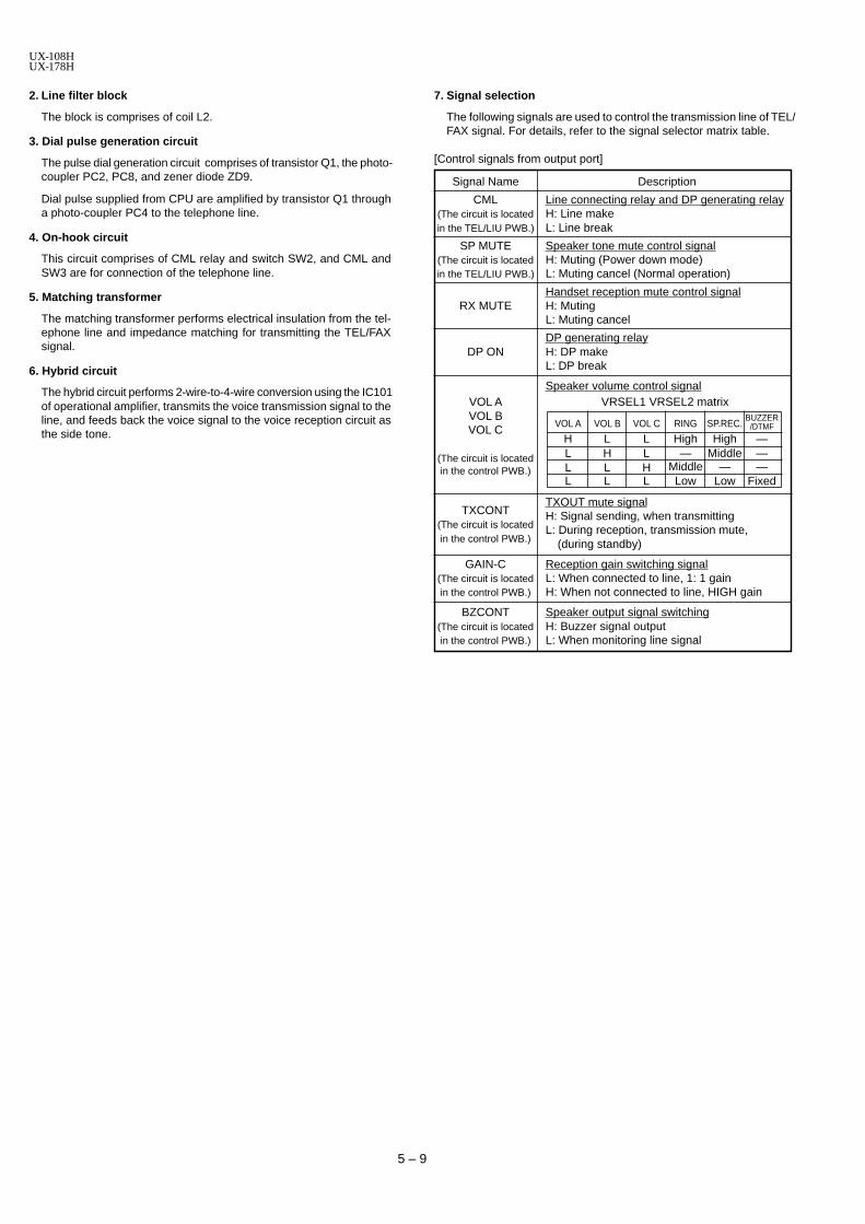
UX-108HUX-178H
5 – 9
2. Line filter block
The block is comprises of coil L2.
3. Dial pulse generation circuit
The pulse dial generation circuit comprises of transistor Q1, the photo-coupler PC2, PC8, and zener diode ZD9.
Dial pulse supplied from CPU are amplified by transistor Q1 througha photo-coupler PC4 to the telephone line.
4. On-hook circuit
This circuit comprises of CML relay and switch SW2, and CML andSW3 are for connection of the telephone line.
5. Matching transformer
The matching transformer performs electrical insulation from the tel-ephone line and impedance matching for transmitting the TEL/FAXsignal.
6. Hybrid circuit
The hybrid circuit performs 2-wire-to-4-wire conversion using the IC101of operational amplifier, transmits the voice transmission signal to theline, and feeds back the voice signal to the voice reception circuit asthe side tone.
Signal Name Description
CML Line connecting relay and DP generating relay(The circuit is located H: Line makein the TEL/LIU PWB.) L: Line break
SP MUTE Speaker tone mute control signal(The circuit is located H: Muting (Power down mode)in the TEL/LIU PWB.) L: Muting cancel (Normal operation)
Handset reception mute control signalRX MUTE H: Muting
L: Muting cancel
DP generating relayDP ON H: DP make
L: DP break
Speaker volume control signalVOL A VRSEL1 VRSEL2 matrixVOL BVOL C
(The circuit is locatedin the control PWB.)
TXCONTTXOUT mute signal
(The circuit is locatedH: Signal sending, when transmitting
in the control PWB.)L: During reception, transmission mute,
(during standby)
GAIN-C Reception gain switching signal(The circuit is located L: When connected to line, 1: 1 gainin the control PWB.) H: When not connected to line, HIGH gain
BZCONT Speaker output signal switching(The circuit is located H: Buzzer signal outputin the control PWB.) L: When monitoring line signal
7. Signal selection
The following signals are used to control the transmission line of TEL/FAX signal. For details, refer to the signal selector matrix table.
[Control signals from output port]
VOL A VOL B VOL C RING SP.REC.BUZZER
/DTMF
H L L High High —L H L — Middle —L L H Middle — —L L L Low Low Fixed

UX-108HUX-178H
5 – 10
(Example: Fax signal send)
8. Cl detection circuit
The CI detection circuit detects the CI signals. A CI signal, which is pro-vided to the photo-coupler PC4 through the C2 (1.8 µF), R2 (10 K), andZD11 when the ring signal is inputted from the telephone line.
9. Power supply and bias circuits
The voltages of +5V and +24VA are supplied from the control PWB unit.
Fig. 6
Signal Name Function
RHSH: The handset is in the on-hook state.
L: The handset is in the off-hook state.
CI Incoming call (CI) detection signal.
[Signals for status recognition according to input signals]
Signal Name Function
TEL IN Receiving signal from line or modem
TEL OUT Transfer signal to line
SPOUT Speaker output signal
TXOUTTransmission (DTMF) analog signal output
from modem
RXINReception (DTMF, others) analog signal input
into modem
[Other signals]NO Signal Name (CNLIUB) NO Signal Name (CNLIUB)
1 EXTSIG 4 DPON
2 N.C. 5 DPMUTE
3 RXMUTE 6 E-RLY
NO Signal Name (CNLIUA) NO Signal Name (CNLIUA)
1 RECMUTE 6 TXOUT
2 CI 7 CML
3 HS 8 +24VA
4 RHS 9 +5V
5 RXIN 10 DG
CI DETECTOR
01
SPEAKER
TEL LINE
+5V+24VADG
CI
RX MUTE
SP MUTE
CI
BZCONT
BZCONTVOL C
VOL BVOL A
EXT.
HANDSET
RXIN
TXOUT
CML
SIGTX
SIGRX0
1
GAIN-C CML
XFC3
MODEM (R96DFXL-CID)
CONTROL PWBTEL/LIU PWB
DP ON
RHS RHS
DP ON
SURGE PROTECTION
BLOCK
LINE FILTER BLOCK
ON-HOOK BLOCK
POLARITY GUARD BLOCK
DIAL PULSE GENERATION
BLOCKSPEECH CIRCUIT BLOCK
DIAL CONTROL
BLOCK
RX MUTE

UX-108HUX-178H
[4] Circuit description of power supply PWB
1. Block diagram
2-1. Noise filter circuitThe input noise filter section is composed of L and C, which reducesnormal mode noise from the AC line and common mode noise to the ACline.
2-2. Rectifying/smoothing circuitThe AC input voltage is rectified by diode D1, 2, 3, 4 and smoothed bycapacitor C5 to supply DC voltage to the switching circuit section.
Power thermistor TH1 suppresses inrush current at power switch-on.
2-3. Switching circuitThis circuit employs the self excited ringing choke convertor (RCC) sys-tem. In this system, the DC voltage supplied from the rectifying/smooth-ing section is converted into high frequency pulses by ON/OFF repeti-tion of MOS FET Q1.
Energy is charged in the primary winding of T1 during ON period of Q1,and discharged to the secondary winding during OFF period.
The output voltage is controlled by adjusting ON period of Q1 whichchanges charge time of C9 through operation of photo-coupler PC1 from+24V output.
[5] Circuit description of CIS unit
1. CISCis is an image sensor which puts the original paper in close contactwith the full-size sensor for scanning, being a monochromatic typewith the pixel number of 1,728 dots and the main scanning density of8 dots/mm.
It is composed of sensor, rod lens, LED light source, light-conductiveplate, control circuit and so on, and the reading line and focus arepreviously adjusted as the unit.Due to the full-size sensor, the focus distance is so short that the setis changed from the light weight type to the compact type.
Fig. 8
Fig. 7
The overcurrent protection is performed by bringing Q1 to OFF statethrough detection of voltage increase in the auxiliary winding of T1 byZD2 and R9.
The overvoltage protection is performed by operating the overcurrentprotection circuit through destruction of zener diode ZD4 and short-circuiting of load.
2-4. +5V circuitEach DC voltage supplied by rectifying the output of transformer T1 withdiode D8 is stabilized by 3-terminal regulator IC1.
2-5. VTH circuitVTH output is supplied through the relay RY1.Relay RY1 is operated by VTH-ON signal.
5ms
2µs0V
2V(TYP)(White original paper)
Approx.5VøT
CISCLK
VO
5 – 11
2. WaveformsThe following clock is supplied from XFC3 of the control board, andVO is output.
NoiseFilter
Circuit
RectifyingSmoothing
CircuitSwitching
Circuit(RCC system)
RegulaterCircuit
+5V
+24V
AC IN
Photo Coupler
F1T1.25A/250V
F34A/72V
F2T1.25A/250V
6 – 1
UX-108HUX-178H
CHAPTER 6. CIRCUIT SCHEMATICS AND PARTS LAYOUT[1
] Con
trol
PW
B c
ircui
t1/
6M
ain
cont
rol b
lock
126 4 35
BD
EF
GI
HC
A
BD
EF
GI
HC
A
126 4 35
A17
107 73 74 75 77 78 79 80 83 84 85 86 87 89 91 92 94 96 97 99 98 101 33 34 35 36 29 31 37
GP
IO20
GP
IO19
GP
IO18
GP
IO17
GP
IO15
GP
IO14
GP
IO13
GP
IO12
GP
IO10
GP
IO9
GP
IO8
GP
IO7
GP
IO6
GP
IO5
VID
CT
L0V
IDC
TL1
CLK
1C
LK2
ST
AR
T
ST
RB
3S
TR
B2
ST
RB
1S
TR
B0
PC
LK
PLA
TS
TR
BP
OL
ADGD72
ADGA
68ADXG
1028148
14
21
28
45
53,56
64,88
95,108
132
7,134
58
VSS
129131
TESTDEBUG
135
RESET
133130
SYSCLK
136137138139141142143
1 2 3 4 5 6 8 9 10 11 12 13 15 16 19 20 22 23 25 26 27 128
127
120
122
121
126
124
125
113
112
111
109
110
61
6260
59
118117116
114
106105104103
52515049
5447
44
A23
A22
A21
A20
A19
A18
A17
A16
A15
A14
A13
A12
A11
A10
BATRST
PWRDWNXOUT
XIN
GPO0GPO1GPO2GPO3
OPI2
OPO2
SM0SM1SM2SM3
OPI0OPI1
OPI3
LCDCSOPO0
CNPN-13SEN2
IC2
XF
C3
70ADVA
41
TSTCLK
144
+5V
76G
PIO
16(6
-2H
)S
PM
UT
E
(4-4
D)
CS
WI
(5-5
F)
VT
HO
N82
GP
IO11
(4-4
D)
(4-5
D)
FR
SN
SI
CN
LIU
A-5
OR
GS
NS
I
CN
LIU
A-4
HS
CI
CN
LIU
A-9
93C
NLI
UA
-3C
NLI
UA
-6
CN
CIS
-5C
NC
IS-4
CN
TH
-12
CN
TH
-11
OPO3OPO4
4342
OPO1 46
CNPN-12SEN3
CNPN-11SEN4
CNPN-14SEN1CNPN-15SEN0CNPN-10E
KEN4AKEN3AKEN2AKEN1A
RA7 470 x 4
TONE 119
(5-5F)TPB(5-5F)TPA
BZOUT (6-1D)
63VBAT
RESET
VBT
R18
6 10
M X2 32.768kHz
C4
4.7/
50R
161
100K C
5 10
/50
17 18A
9A
8A
7A
6A
5A
4
A2
A1
A0
RD
WR
RO
MC
SC
S1
MC
SS
YN
CR
EG
DM
AW
AIT
RA
SC
AS
0C
AS
1D
WR
WR
PR
OT
A16
A15
A14
A13
A12
A11
A10 A9
A8
A7
A6
A5
A4
A3
A2
A1
A0
32
C12
2 0.
1
+5V
RA3 270 x 4
90G
PIO
4
100
CLK
1
30P
DA
T
24A
3
57C
S0
GP
IO3
GP
IO2
GP
IO1
GP
IO0
R12
6
R20
3 3.
3K
RA
1 10
K
RA
1 10
K
RA
1 10
K
(3-2
A)
MD
MR
ST
(4-3
D)
CU
T1I
CN
LIU
B-4
CN
TH
-6
DP
ON
RA
NK
(4-3
D)
PS
NS
I
(3-1
D)
BY
PA
SS
(4-5
D)
DR
SN
SI
TE
LMU
TE
RH
S
R16
2 47
0
R20
6 47
0R
159
470
R25
5 47
0R
234
470
R23
5 47
0 R12
5
R23
9 47
0R
236
470
R24
0 47
0R
A1
10K
ST
RB
3
CN
TH
-4S
TR
B2
CN
TH
-3P
CLK
DA
TA
CN
TH
-14
CN
TH
-15
CN
TH
-13
LAT
CH
R12
2 47
0R
121
470 R20
7 27
0R
208
270
R20
9 27
0R
210
270
R21
1 27
0R
212
270
R21
3 27
0
ST
RB
4
CIS
CLK
ST
RB
1
R16
8 10
K
C208 1000PC205 1000PC177 1000P
C210 1000P
C199 1000PC181 22PC182 1000P
OPO5 40
OPO6 39
OPO7 38
55LEDCTLCNPN-1CNPN-2CNPN-3CNPN-4
R187 470
L104 Z2104
RA
6 27
0x4
(4-4D)
C126 2200P
C141 15P
C140 22P666765
–VREF/CLREF
VINTHADI
+VREF 71
VDRAM
(5-2D)THADI(5-5D)VIN(5-4D)–VREF(5-4D)+VREF
(5-5F)TPB(5-5F)TPA
(6-4A)GAINC
(6-3H)BZCONT(5-2A)
VREFCONT
(6-6A)TXCONTRA2
270x4115
C10
5 0.
1
+5V
(2-3
C)(
3-3A
)(2
-3E
)(3-
3A)
(2-3
D)
(2-3
E)
CE
1
(3-3
A)
MC
S
RD
WR
RD
MC
S
A[1
6~0]
69C12
3 0.
1
140123
C11
4 0.
1
C12
8 0.
1C
127
0.1
C12
5 0.
1
C10
6 0.
1C
124
0.1
C10
8 0.
1C
104
0.1
SYSCLK(3-2A)
RA4 270 x 4
D7D6D5D4D3D2D1D0
RA5 270 x 4
D7D6D5D4D3D2D1D0
D[7
~0]
MIRQ(3-2A)
R128 10K
C107 1000P
R105 10K
R108 10K
R167 10K
MIRQ
VSS
VSS
VSS
VSS
VSS
VSS
VSS
VDDVDDVDDVDDVDDVDDVDDVDD
R10
9
R21
4
C159 100PC160 100PC161 100PC139 100PC138 100P
C13
7
N.M
.
R165R163R164R166
10K
x4
C153 100PC119 100PC118 100PC120 100P
N.M
.
R12
3 47
0(*
1)
L101
0
C11
5 0.
1
R11
0R
133
R13
4
R13
9R
140
R13
1R
132
R13
7R
138
R12
9R
130
R13
5R
136
R17
0R
171
R17
4R
175
R16
927
027
027
027
027
027
027
027
027
027
027
027
027
027
027
0
270
270
270
R10
7
R18
8R
103
270
270
270
270
270
C184 82PC185 82PC188 82PC186 82P
C187 82P
C204 0.1C193 82P
R12
4 47
0
R12
7 47
0
R12
0
R16
0
C15
6 18
PC
151
18P
TΦ
TΦ
(*1)
RA
1 10
K
MO
DE
LU
X-1
08H
UX
-178
H
R12
0
N.M
.47
0
R12
5R
126
N.M
.N
.M.
470
30K
(*1)
ΩΩ
Ω
CM
L
RA
1 10
KR
A1
10K
RA
1 10
K
6 – 2
UX-108HUX-178H
Mem
ory
bloc
k2/
6
126 4 35
BD
EF
GI
HC
A
126 4 35
BD
EF
GI
HC
A
30N
CR
229
N.M
.
A17
A16
21A
1520
A14
2919
A13
2818
A12
17A
1125
15A
1023
14A
926
13A
827
A7
A6
32A
531
A4
1A
3A
210
A1
1116
A0
12 22 24
1IO
819
26IO
718
A14
2
A14
IO6
17A
13
23
A13
IO5
16A
12
21
A12
IO4
15A
11
24
A11
IO3
13A
10
25
A10
IO2
12A
9
3
A9
IO1
11A
8
4
A8
A7
5
A7
A6
6
A6
A5
7
A5
VD
D28
A4
8
A4
VS
S14
A3
9
A3
A2
10
A2
A1
A0
20
A0
27W
E22
CS
2/O
E
A[1
6~0]
(1-5
I)
D[7
~0]
(1-6
I)
(1-3
I)
RD
(1-3
I)
+5V
C17
8 0.
1
D7
D6
D5
D4
D3
D2
D1
D0
IC7
27C
010
2A
16D
73
A15
D6
A14
D5
A13
D4
4A
12D
3A
11D
2A
10D
1A
9D
0A
85
A7
6A
6V
CC
7A
5P
GM
8A
4V
PP
9A
3A
2A
1G
ND
A0
CE
OE
IC5
W24
257S
–70L
A1
CS
1
D7
D6
D5
D4
D3
D2
D1
D0
VB
T
C14
2 0.
1
WR
(1-3
I)C
E2
(4-1
D)
CE
1(1
-3I)
VB
T
R18
9 22
K
R19
0
R17
3 0
N.M
.
RO
MC
S

6 – 3
UX-108HUX-178H
Mod
em b
lock
3/6
126 4 35
BD
EF
GI
HC
A
BD
EF
GI
HC
A
126 4 35
R15
2 10
R157 470
R156 470
N.M
.
R15
4 10
C10
3N
.M.
+5V
D7
A0
C11
3 0.
01
R10
6 27
0
D6
D5
D4
D3
D2
D1
D0
A1
A2
A3
A4
56 57 58 59 60
RS
4R
S3
RS
2R
S1
RS
0
8D
79
D6
10D
511
D4
12D
313
D2
14D
115
D0
54C
S55
RE
AD
53W
RIT
E52
IRQ
70X
CLK
(12M
)71
YC
LK(6
M)
64R
TS
78C
TS
79
DC
LK82
DC
LKI
73
RX
D95
TX
D
96R
LSD
67P
OR
I65
EN
85
DG
617576949391
72
2350
67
1666778081899297
22
L102
0
C11
7 1
GP13GP16GP17GP19GP20GP21
+5VD1
0VD10VD10VD20VD20VD20VD20VD20VD20VD20VD20VD20VD2
C13
3 1
+5VD2+5V
L103
0
+5V
A0V
A0V
A0V
A0V
A0V
A
46
AD
OU
TA
DIN
RC
VO
RC
VI
RA
MP
INA
GD
SW
GA
IN0
SW
GA
IN1
N.C
.N
.C.
N.C
.
17 21 30 43 47
C10
0 0.
1
35 87 98 37 45 49 18 48 42 44 88 99 24 19 27 29 31 32
C3
47/2
5
R11
6 3
+5V
R10
1 0
MA
G
N.C
.33
SIG
RX
5432110063
383940
8525832674848690
68
GP07GP06GP05GP04GP03GP02GP11
TXLOSS2TXLOSS1
EYECLKECLKIN1
EYESYNCSYNCIN1SYNCIN2
EYECLKXEYEXEYEY
XTLI
E-RLYVOLCVOLA
(6-1H)CNLIUB-5
(6-1H)(6-2H)
R15
3 0
MA
GX
1 24
.000
14M
Hz
C10
1 27
P
R10
2 12
0
C10
2 27
P
R11
9 20
0
69XTLO
IC4
R96
DF
XL-
CID
N.C
.N
.C.
N.C
.
DG
(6-3
A)
DPMUTEVOLB
D[7
~0]
RD
WR
(1-6
I)
(1-3
I)(1
-3I)
(1-3
I)
DG
C12
1 1
R10
0
(5-5F)
DG
62N.C.
R11
5 10
K
LEDON
DG
C13
1 1
51
RX
IN
41
DA
IN34
AO
UT
N.C
.2820
N.C
.N
.C.
N.C
.
DA
OU
TT
XO
UT
MA
G
C11
0 1
C11
6 39
0P
C11
2 0.
1R
113
47.5
KA
GD
(6-3
A)
SIG
TX
(6-5
A)
36BYBASS
DG
R158 470R145 470R146 470R155 470
CNLIUB-3RXMUTE
MIR
Q(1
-6F
)
A[4
~0]
(1-5
I)
SY
SC
LK(1
-6F
)
MD
MR
ST
(1-5
H)
MC
S
R10
4 10
0
MA
G
R11
8 10
K
TXLOSS3
(1-4D)BYPASSR147 10K
R11
7 10
K
L100
27
0
R18
4 27
0
R15
0 0
R14
9 0
MA
GD
G
DG
(6-2H)
C19
1 82
PC
190
82P

6 – 4
UX-108HUX-178H
Oth
er b
lock
4/6
126 4 35
BD
EF
GI
HC
A
126 4 35
BD
EF
GI
HC
A
IC10
0 P
ST
596C
NR
+5V
35
4
OUT
GN
D
2
MR
ST
R19
2Q
100
VC
C
R19
1
RE
SE
T
R17
6 1K
SU
B
1C
129
1
1
32
– +
R22
7N
.M.
C13
6 10
00P
C20
6 10
00P
C20
7 0.
1
R2
10(1
/4W
)
DG
C19
7 10
00P
CN
PN
-6
+5V
C13
4 10
00P
MG
DG
C17
5
C17
4
C20
2
C20
1
MG
R23
2
R21
5R
230
+5V
R25
2 27
0C
NP
N-8
OR
GS
NS
R24
5 5.
6K
R25
0 3.
3K
R24
8 30
K
IC9
2904
(1-4
A)
OR
GS
NS
1
C19
4 0.
1
4
(1-4
A)
DR
SN
S1
(1-4
A)
(1-5
H)
(1-4
A)
CN
PN
-9F
RS
NS
CN
CS
W-1
CS
WI
CN
CU
T1-
1C
UT
I1
C14
3 22
00P
R17
2 27
0
C13
5 22
00P
R18
5 27
0
C17
2 22
00P
R22
6 27
0
C14
4
FR
SN
S1
CS
WI
CU
T1I
SW
1 D
OO
R S
W
(1-4
A)
PS
NS
I+
5VR
141
13
24
PI1
DG
BA
TH
LD-1
BT
+
R25
4 5.
6K
CN
PW
-2+
5V
BA
TH
LD-2
BA
TH
LD-3
DG
BA
T1
CR
2032
DG
D10
1 R
B70
5D
+5V
DG
C19
5 0.
1
<V
BT
>
VB
T
+5V
CN
PW
-1D
G
CN
LIU
A-1
1+
5V
CN
LIU
A-1
2
CN
CU
T1-
2D
G
CN
PN
-7+
5V
CN
PN
-5D
G
C21
1 0.
1C
7 47
/25
DG
CN
PW
-7+
24V
CN
PW
-4C
NP
W-5
CN
PW
-6
CN
LIU
A-1
0+
24V
A
C20
9 10
00P
C10
22
/50
R23
1
+24
V
MG
N.M
.
+24
VA
DG
C8
100/
50
DG
FG
R23
3
N.M
.
N.M
.
R19
3
8
N.M
.
C15
8 22
00P
(*1)
(*1)
(*1)
(*1)
MO
DE
LU
X-1
08H
UX
-178
H
CN
CU
T1
N.M
.N
.M.
2PIN
270
N.M
.C
144
2200
P
R19
3R
141
PI1
N.M
.N
.M.
220K
ITR
9606
(*1)
ΩΩ
CE
2(2
-3E
)
(1-1
F)
DG

6 – 5
UX-108HUX-178H
Vid
eo p
roce
ssin
g/M
otor
driv
e/th
erm
al b
lock
5/6
126 4 35
BD
EF
GI
HC
A
126 4 35
BD
EF
GI
HC
A
– +
–+
C20
0 10
00P
C17
9 10
00P
L105
0
C20
3 0.
1
C25
8 22
KC
213
1000
P
R18
0 10
00P
C19
8
N.M
.
C17
3 10
00P
C164 1000PC165 1000PC163 1000PC162 1000PC176 1000PC196 82P
+5V
R20
4 5.
1KQ
101
2SC
2412
Q10
2 2S
A10
37
R20
5 1.
5KR
202
10K
CN
CIS
-1V
O(1
-1F
)V
IN
C15
7 10
00P
+5V
R24
2 10
K
R24
1 30
K
IC8
2902
321
(1-1
F)
VR
EF
+
(1-1
F)
VR
EF
–
+5V
+24
V
+5V
CN
CIS
-3+
5V
CN
CIS
-2D
G
CN
CIS
-7+
24V
CN
CIS
-6G
LED
C15
5 10
00P
R25
5
IC9
2904
657
R22
4 R
228
R25
3
R24
9
R1
R24
6
Q1
Q10
3
E
BC
(1-1
E)
VR
EF
CO
NT
(5-5
I)LE
DO
N
CO
M9
11B
1C16
22B
2C15
33B
3C14
44B
4C13
55B
5C12
66B
6C11
77B
7C10
8E
TP
AT
PB
(1-1
E)
TP
A(1
-1E
)
TP
B(1
-1E
)(1
-1E
)
(1-4
A)
VT
HO
N
(3-1
D)
LED
ON
IC10
U
LN20
03A
CN
MT
-5C
NM
T-6
CN
MT
-1C
NM
T-2
CN
MT
-3C
NM
T-4
CN
PW
-3LE
DO
N(5
-1B
)
+24
V
D1
MP
ZP
4748
FU
100
1CP
-S0.
7
MG
MG
VT
HC
NP
W-8
VT
HC
NT
H-1
CN
TH
-2C
NT
H-1
6
MG
CN
TH
-7C
NT
H-8
CN
TH
-9
CN
PW
-9C
NP
W-1
0C
212
1000
P
MG
+5V
CN
TH
-10
TH
AD
I(1
-1F
)
TH
IC
NT
H-5
MG
MG
C18
3 0.
1R
257
20K
C9
10/5
0R
256
470K
+5V
<V
IN>
<V
O>
VG
VT
H
MG
VT
H
MG
C15
4 0.
1
(*1) MO
DE
LU
X-1
08H
UX
-178
HN
.M.
N.M
.B
CR
133
Q1
Q10
3R
127
(1
W)
N.M
.
R22
433
K
N.M
.
R22
5R
228
R24
6R
249
30K
30K
0
0
0N
.M.
N.M
.N
.M.
R25
320
0
N.M
.
(*1)
ΩΩ
ΩΩ
Ω2S
D18
58
ΩΩ
Ω

6 – 6
UX-108HUX-178H
Ana
log
sign
al b
lock
6/6
126 4 35
BD
EF
GI
HC
A
BD
EF
GI
HC
A
126 4 35
– +
– +
– +
– +
6 12
C19
2 82
P13
1314
12
TE
LOU
TC
NLI
UA
-1
R22
0 86
.6K
C17
0 68
0P
C13
0 1
IC6
4053
VR
EF
TX
CO
NT
(1-1
E)
01
89 10
IC8
2902
R21
7 17
.4K
+5V
R21
6 3.
3KC
166
1
+5V
16 7 8
IC6
MC
1405
3BF
C14
9 0.
1
SIG
TX
(3-3
H)
R17
8 1K
R17
7 0
R19
4 0
C13
2 1
R21
8
R23
8 10
K
C14
5 T
XO
UT
CN
LIU
A-8
SIG
TX
(3-3
H)
R22
1 86
.6K
C16
9 10
00P
76 5
IC8
2902
SIG
RX
(3-3
H)
+5V
D10
0 1S
S35
5
R22
3 3K
MA
G
AG
D(3
-3H
)
R19
5 0
C6
10/5
0
54
3
9 IC6
4053
01
GA
INC
(1-1
E)
RX
INC
NLI
UA
-10
R20
1 11
8K
R20
0 11
8K
R19
8 E
XS
IGC
NLI
UB
-1
C14
8 0 R19
6 0
E-R
LY(3
-1C
)
R23
7
1413 12
+24
VA R24
3
C16
8 0
R24
4
R21
9
TE
LIN
CN
LIU
A-2
C18
9
C16
7 0.
1
114
E-R
LYC
NLI
UB
-6
VR
EF
+5V
C14
6
R24
7 33
K
IC8
2902
R22
2 33
KC
171
1
115
2
10
IC6
4053
1 0
R17
9 1K
C15
2 47
00P
IC3
4066
R14
3 10
K
R14
8 30
K
IC3
4066
89
1011
C15
0 0.
01R
199
3K
R14
4 22
0K
R18
2 10
K
R11
1 3K
C1
1/50
5
IC1
MC
3411
98
71
32
46
R15
1 10
K
+5V
R11
4 10
0KR
112
150K
C10
9 33
0P
SP
+C
NS
P-1
SP
–C
NS
P-2
SP
MU
TE
(1-5
A)
BZ
CO
NT
(1-1
E)
VO
LB(3
-1C
)
VO
LA(3
-1C
)
BZ
OU
T(1
-1F
)
VC
C
GN
DV
EE
EN
AB
LE6
+5V
14 7 3,4,
5
IC3
4066
C11
1 0.
1
VC
C
GN
D
11
C14
7 0.
1
R19
7 20
K
R25
1 33
K
R14
2 10
0K
IC3
4066
12
VO
LC(3
-1C
)
R18
0 10
K
R18
1 10
K
C2
4.7/
25
R18
3 10
K
N.M
.N
.M.
N.M
.
N.M
.
(*1)
N.M
.
N.M
.
N.M
.
N.M
.N
.M.
(*1) M
OD
EL
UX
-108
HU
X-1
78H
R23
7
N.M
.0
ΩΩ
6 – 7
UX-108HUX-178H
Control PWB parts layout (Top side)

6 – 8
UX-108HUX-178H
Control PWB parts layout (Bottom side)
6 – 9
UX-108HUX-178H
[2] T
EL/
LIU
PW
B c
ircui
t1/
3
126 4 35
BD
EF
GI
HC
A
126 4 35
BD
EF
GI
HC
A
– + – +
– +
2904
1
32– +
8 4
JP11
1
JP11
3
N.M
.
JP104
JP110
JP1
L1 JP2
JP3
L2
N.M
.
JP4
JP11
4
N.M
.JP
112
AR
1 R
A50
1PV
6
AR
2 R
A50
1PV
6
JP10
7
N.M
.
JP10
8
JP106
CM
L
CM
L5
4
398 10
JP102
JP10
5Z
D3
BZ
X79
B3V
9 ZD
4 B
ZX
79B
3V9
D2
1SS
82
SW
11
2
3S
W2
PC
5 T
LP62
0 C1
47/1
0(N
.P.)
R10
1 91
ZD
1 H
ZS
3B1
ZD
2 H
ZS
3B1
R10
2 0
TE
L1
TE
L2
TE
L3
PC
6 T
LP62
7
C10
7 0.
1
R2
10K
(1W
) Z
D11
B
ZX
79B
30V
D1
1SS
131
PC
4 T
LP52
1
DG
DG
C1
CN
LIU
A-4
+5V
R1
110K
(1/2
W)
T1
Z21
40
R15
1 20
K
VR
EF
+5V
R13
7 10
0K
PC10 R156
N.M
.
DG
N.M
.P
C10
+24
VA
CM
L1
12
DG
Q11
0 B
CR
133
CN
LIU
B-1
CN
LIU
A-9
CM
L
EX
TS
IG
D4
1SS
133
C11
0 0.
1
R15
4 13
0K
C12
1
ZD
14
HZ
2A1
N.M
.
ZD
15
HZ
2A1
VR
EF
R14
3 20
KV
RE
F
R15
3 20
K
R14
1 20
KR
144
1.6K
R14
5 0
C11
4C
113
N.M
.
VR
EF
2904
7
56
IC10
1
C10
9 0.
1
R14
2 68
K
C10
8 82
0P
ZD
12
HZ
2A1
ZD
13
HZ
2A1
RX
INC
NLI
UA
-7
CN
LIU
A-8
TX
OU
T
VR
EF
R15
5 22
KC
120
0.1
DG
DG
34
18
2
C11
2 0.
1
C11
6 12
00P R14
8 56
K
R14
7 24
0R
152
560
R14
9 10
K
C11
9 N.M
.
Q11
1 2S
J106
VR
EF
A B
(2-6
I)
IC10
2
R15
8 20
K
R15
7 20
K
C12
2 0.
1
C15
10
/50
C16
10
/50
DG
DG
DG
DG
DG
VR
EF
C11
5 R
146
1K
N.M
.
(2-6
A) (2
-5I)
(2-6
A)
(2-4
A)
CN
LNJ-
1
CN
LNJ-
2
CN
LNJ-
3
CN
LNJ-
4
CN
LNJ-
5
CN
LNJ-
6
TLJ
-1
TLJ
-2
TLJ
-3
TLJ
-4
T1/
B-W
IRE
L1/S
HU
NT
L2/E
AR
TH
T2/
A-W
IRE
EA
RT
H
EA
RT
H
T1
T2
SH
UN
T
N.M
.
CN
BZ
-1
CN
BZ
-2
CN
BZ
-3
CN
BZ
-4
AR
G
JP10
9
C2
1.8
R15
0 20
K6 5
714
58
D
G
S
1458
2904
4 56
IC10
2
+24
VA
+24
VA
+24
VA IC
101
JP101
N.M
.
N.M
.
N.M
.
N.M
.
NO
TE
:T
hese
mar
ks a
re a
ll sa
fety
-crit
ical
par
ts.
R3
100(
1W)
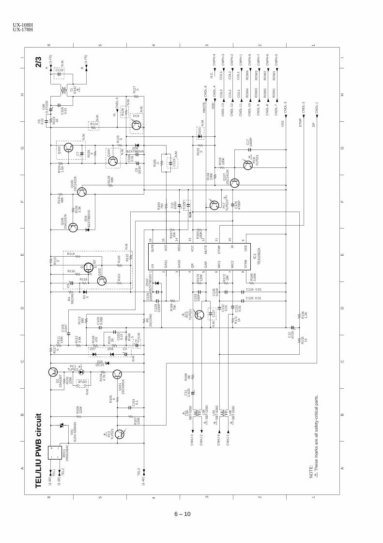
6 – 10
UX-108HUX-178H
TE
L/LI
U P
WB
circ
uit
2/3
126 4 35
BD
EF
GI
HC
A
BD
EF
GI
HC
A
126 4 35
C10
10
/50
C12
3N
.M.
910111213141516
87654321LN G
AS
1
GA
S2
QR
GA
R
MIC
1
MIC
2
ST
RB
SLP
E
AG
C
RE
G
VC
C
MU
TE
DT
MF IR
VE
E
IC1
TE
A10
62A
R16
7 15
K
R16
3 10
0K
C12
5 47
00P
Q10
7 2S
C24
12K
PC
8 T
LP52
1
C17
10
00P
R13
4 10
0K
CN
DL-
2
CN
DL-
1
CN
DL-
3V
SS
DT
MF
DP
CN
DL-
4
CN
DL-
6
VD
D
XM
UT
E
R13
3 10
0K
C12
8
N.M
.N
.M.
R16
4 75
K
R13
2 0
D10
1 N
.M.
CN
DL-
13
CN
DL-
12
CN
DL-
11
CN
DL-
10
CN
DL-
9
CN
DL-
8
CN
DL-
7
CN
PH
-3
CN
PH
-2
CN
PH
-1
CN
PH
-8
CN
PH
-7
CN
PH
-6
CN
PH
-5
N.C
.C
NP
H-4
CO
L3
CO
L2
CO
L1
RO
W4
RO
W1
RO
W3
RO
W2
CO
L3
CO
L2
CO
L1
RO
W4
RO
W1
RO
W3
RO
W2
R16
9 75
K
C12
9 12
00P
C13
4 10
00P
ZD
10
BZ
X79
B10
V
R17
0 12
0K
C13
3 33
0P
C12
7 N
.M.
PC
7 T
LP52
1
PC
3 T
LP52
1
R17
2 18
K
C13
0 0.
018
C13
2 0.
01
C13
1 0.
01R
171
1K
C124 0.01
C126 0.01
R16
6 3.
65K
C12
47
/25
R13
6 1.
2KR
135
1K
CN
HJ-
1
CN
HJ-
4
CN
HJ-
2
CN
HJ-
3
TE
L3
TE
L2
TE
L1(1
-6E
)
(1-5
E)
(1-4
E)
RE
C1
OR
5G4B
42
~
+
~
–
VA
1 S
10V
-S05
K60
R10
6 22
0K
R10
3 10
0K
Q1
2SA
1807
JP103
PC1 TLP521
Q10
1 2S
C40
61KR
104
4.7K
PC
2 T
LP52
1
R10
7 12
0K
C10
1 0.
1
ZD7 ZD6 C4
N.M
.
ZD5 IZC15
C3 R10
8 0
C10
2 0.
22
R11
0 2KR10
9 47
0
R11
2 3.
9K
C10
4 0.
047
R11
3 68
0
C10
3 0.
068
R5
20(1
/2W
)
R4
56(1
W)
D3 0
C5
R118
R116
R119
Q2
Q10
2
R12
1R
120
N.M
.
D
G
S
R16
5 0
R12
9 68
K
C9
33/1
0
C10
6 0.
01
ZD8 BZX79B5V6
N.M
.
PC9
Q10
4
N.M
.
N.M
.
N.M
.
R12
5 0
R12
6 0
R114
C7Q10
3R
124
1.6K
R12
3 1KC6
0.22
C68
0.
47/1
00
C10
5 0.
01
T2
I214
2
N.M
.
C118
(1-F
5)
CN
DL-
5
(1-F
5)
VL
N.M
.
R12
8
R12
7 0
Q10
5 2S
C24
12K
Q10
6 2S
A10
37K
R13
0 3.
3K
R13
1 68
K
ZD
9 B
ZX
79B
5V6
R11
5 0
L3A
S
BT
-026
0
L4A
S
BT
-026
0
R16
8 68
C11
3.
3/25
R11
1 13
0K
R11
7 0
R10
5 0
A B
N.M
.
N.M
.
NO
TE
:T
hese
mar
ks a
re a
ll sa
fety
-crit
ical
par
ts.
R12
2
L3B
S
BT
-026
0
L4B
S
BT
-026
0

6 – 11
UX-108HUX-178H
TE
L/LI
U P
WB
circ
uit
3/3
126 4 35
BD
EF
GI
HC
A
BD
EF
GI
HC
A
126 4 35
DG
+5V
CN
LIU
A-1
1+
5V
CN
LIU
A-1
2D
G
+24
VA
+24
VA
C14
47
/25
C11
7 22
3C
E-R
LYC
NLI
UB
-6
DG
Q10
8 B
CR
133
+5V
PC
6 T
LP62
7R
138
470
TE
LMU
TE
CN
LIU
B-5
DG
DP
MU
TE
CN
LIU
B-3
DG
RX
MU
TE
CN
LIU
A-3
DP
ON
CN
LIU
B-4
DG
DG
C11
1 22
3CC
13
22/5
0
PC
8 T
LP52
1
PC
7 T
LP52
1
PC
3 T
LP52
1
PC
2 T
LP52
1
R16
0 47
0
R16
1 47
0
R16
2 47
0
R14
0 47
0
Q11
4 B
CR
133
Q10
9 B
CR
133
Q11
2 B
CR
133
Q11
3 B
CR
133
CN
LIU
A-1
0
CN
LIU
A-6
DG
SW
2
31
RH
S
+5V
PC
9
R15
9
DG
N.M
.
HS
CN
LIU
A-5
DG
+5V
PC
1 T
LP52
1
PC
5 T
LP62
0
R13
9 10
0K
NO
TE
:T
hese
mar
ks a
re a
ll sa
fety
-crit
ical
par
ts.

6 – 12
UX-108HUX-178H
TEL/LIU PWB parts layout (Top side)

6 – 13
UX-108HUX-178H
TEL/LIU PWB parts layout (Bottom side)

6 – 14
UX-108HUX-178H
[3] P
ower
sup
ply
PW
B c
ircui
t
126 4 35
BD
EF
GI
HC
A
126 4 35
BD
EF
GI
HC
A
4 3
RL1
N40
05 x
4
C5
68/4
00
R2
0.33
(2W
)
C7
220P
INO
UT
GN
D
L1
C1
0.1
V1
470V
F1
T1.
25A
/250
V
CN
1
Q1
FS
5KM
-18A
R5
560K R6
560K
R7
220K
(2W
)
D5
05N
U42
C6
1500
P
T1
D7
S3L
20U
-400
4P15
C16
22
00P
C15
68
0/35
ZD4 RD30FB3
R19
R12
2.
2KQ
3 2S
C17
40S
PC
1 P
C12
3FY
8
R13
27
0R
14
6.8K V
R1
470
R15
2.
4K
7 10
VM
IC1
NJM
78M
05F
A1
3
2
C18
47
0/16
D8
SR
140
R10
33
D6
IS20
76A
PC
1 P
C12
3FY
8
1 2
C4
1000
P
AC
LA
C N
R3
15K
C9
0.06
8
R4
100
Q4
2SC
1741
AS
QR Q
2 2S
C26
55-Y
C10 1000P
C11 1000P
ZD2 RD3.3ESAB2 R
9 56
0
R8
820
C8
4700
P
C13
22
00P
C17
10
00P
6M
G
VT
H
MG
MG
5 4
+5V
2
DG
1CN
2
31
R1
560K
C3
1000
PD3
D2
D4
D1
TH
1 M
1600
7C
C20
22
00P
R16
82
0
R11
56
0
C14 1000P
(5)
(1)
(2)
(3)
(6)
(7)
(8)
(4)
C19
1/
50
ZD3 RD6.2ESAB2N
.M.
9V
TH
8V
TH
3V
TH
-ON
FB
1F
3 C
CP
2E10
0
D9
IS20
76A
RY
1 A
JS33
12
C2
0.1
F2
T1.
25A
/250
V

6 – 15
UX-108HUX-178H
Power supply PWB parts layout

6 – 16
UX-108HUX-178H
[4] O
pera
tion
pane
l PW
B c
ircui
t
Not
e: S
ince
the
part
s of
this
PW
B c
an n
ot b
e su
pplie
d, c
hang
e it
as a
uni
t.
126 4 35
BD
EF
GI
HC
A
126 4 35
BD
EF
GI
HC
A
CN
PN
-15
CN
PN
-14
CN
PN
-13
CN
PN
-12
CN
PN
-11
SE
N0
SE
N1
SE
N2
SE
N3
SE
N4
KE
N 1
A
CN
PN
-3K
EN
2A
CN
PN
-2K
EN
3A
CN
PN
-1K
EN
4A
CN
PN
-10
E
CN
PN
-7+
5V
CN
PN
-6G
ND
CN
PN
-5
FU
NC
RE
CE
PT
ION
RE
SO
LUT
ION
PLA
Y
RE
MIN
DE
R
CO
PY
DE
LET
E
8 02
D1
D2
D3
D4
D5
D6
D7
D8
D9
11 12 13 1 2 3 4 5 10
A0
A1
A2
A3
9 7 6 14
IC10
1 74
HC
147
CN
LCD
-6C
NLC
D-5
CN
LCD
-3C
NLC
D-2
CN
LCD
-1
C2
22/5
0C
1 0.
022
CN
LCD
-11
LD4
CN
PN
-4
GN
D
CN
LCD G
ND
1 2 3 4 5 6 7 8 9 10 11 12 13 14
+5V
VO
RS
GN
DE N
.C.
N.C
.N
.C.
N.C
.LD
4LD
5LD
6LD
7
CN
PN
KE
N 4
AK
EN
3A
KE
N 2
AK
EN
1A
+5V
GN
DG
ND
OR
GS
NS
FR
SN
SE S
EN
4S
EN
3
DO
WN
01
UP
02
ST
OP
ST
AR
T
5
RE
C
9 #3 6
HO
LD
SP
EA
KE
R
SP
EE
D
RE
DIA
L
07 0903 05
08 1004 06
71 4
D5
1SS
270
D4
1SS
270
D3
1SS
270
D1
1SS
270
CN
LCD
-12
LD5
CN
LCD
-13
LD6
CN
LCD
-14
LD7
D2
1SS
270
CN
LCD
-4R
S
15N
.C.+5V
VC
C
GN
D 816
R1
6.2K R8
1K
VO
+5V
CN
PN
-8
CN
PN
-9
R7
220
SG
266
OR
GS
NS
AC E
K
FR
SN
S
OR
GS
NS
SE
N2
SE
N1
SE
N0
RE
PE
AT
FR
SN
S
1 2 3 4 5 6 7 8 9 10 11 12 13 14 15
R10 100K
R5 100K
R9 100K
R3 100K
R2 100K
R4 100K
R11 100K
R12 100K
R6 100K

6 – 17
UX-108HUX-178H
M E M O

UX-108HUX-178H
7 – 1
CHAPTER 7. OPERATION FLOWCHART
[1] Protocol
NSF
DIS
NSS
TCF
CED
NSF
DIS
NSS
TCF
RTC
MPS
CFR
RTC
MPS
MCF
RTC
EOP
MCF
MCF
DCN
CFR
TSI
CSI
CSI
TSI
RTC
EOP
MCF
DCN
IMA
GE
SIG
NA
L
Document ejectedRecording papor ejected
Receive sideG3 communication
CED
Transmitter side(Document inserted into document sensor during standby)
To recordingposition
(DCS)
Cut line printed
IMA
GE
SIG
NA
L
Cut line printed
IMA
GE
SIG
NA
LIM
AG
ES
IGN
AL
Next page insertcommand
1st page
Document inserted tothe reading position
(DCS)

UX-108HUX-178H
7 – 2
[2] Power on sequence
2
1YES
YES
CPU initialized
MODEM initialized
STOP key ?
“WAIT A MOMENT” display
START
NO
YES
STAND-BY
3 sec ?NO“MEMORY CLEAR ?” display
NO
YES
STAND-BY
3 sec ?NO
NO
START key ?
COPY key ?
STOP key ?
NO
Memory clear
STAND-BY
21
“MEMORY CLEARED” display
Memory clear
PROCESS CHECK MODE
“MEMORY CLEARED” display
YES

UX-108HUX-178H
8 – 1
CHAPTER 8. OTHERS
[1] Service tools
1. List
Relay board unit
NO. PARTS CODE DESCRIPTION Q’TYPRICERANK
1 C P W B S 2 9 1 5 S C S 1 Relay board unit 1 BN2 P S H E Z 3 3 5 4 S C Z Z Shading wave memory standard paper 1 AD
1 C C N W – 4 7 5 6 S C 0 1 SPEAKER RELAY CABLE 1 AK2 C C N W – 4 7 5 7 S C 0 1 PANEL RELAY CABLE 1 AW3 C C N W – 4 7 5 8 S C 0 1 CIS RELAY CABLE 1 AQ4 C C N W – 4 7 5 9 S C 0 1 HEAD RELAY CABLE 1 AX5 C C N W – 4 7 6 0 S C 0 1 CAM SWITCH RELAY CABLE 1 AK6 C C N W – 4 7 6 1 S C 0 1 CUTTER SWITCH RELAY CABLE 1 AK7 C C N W – 4 7 6 3 S C 0 1 MOTOR RELAY CABLE 1 AP8 Q C N W – 4 7 6 4 S C Z Z PAPER SENSOR RELAY CABLE 1 BB9 V H P R P i – 5 7 4 / / / PHOTO TRANSISTOR [PSNS] 1 AF
10 V R S - T S 2 A D 2 2 1 J RESISTOR (1/10W 220Ω ±5%)[R100] 1 AA11 Q P W B S 2 9 1 5 S C Z 4 EXTENSION PWB 1 AR
NO. PARTS CODE DESCRIPTION Q’TYPRICERANK
PSNS(TP3)
PI1
DG(TP1)
+5V(TP2)
R100
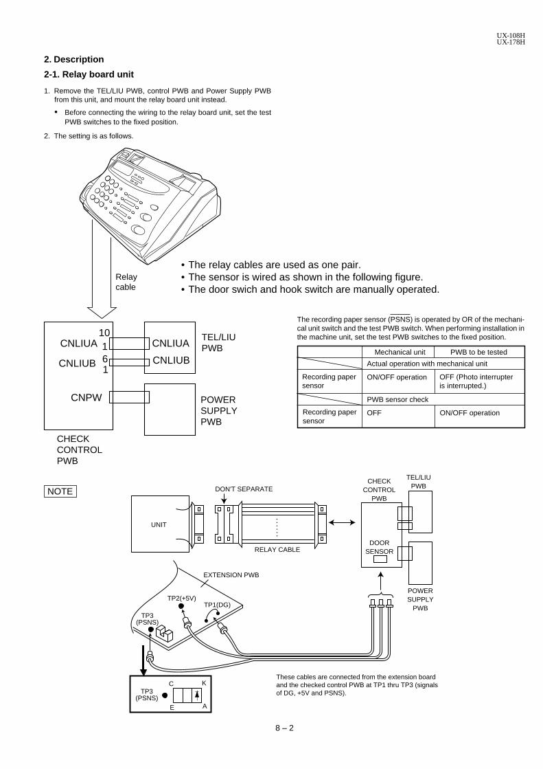
UX-108HUX-178H
8 – 2
2. Description
2-1. Relay board unit
1. Remove the TEL/LIU PWB, control PWB and Power Supply PWBfrom this unit, and mount the relay board unit instead.
• Before connecting the wiring to the relay board unit, set the testPWB switches to the fixed position.
2. The setting is as follows.
The recording paper sensor (PSNS) is operated by OR of the mechani-cal unit switch and the test PWB switch. When performing installation inthe machine unit, set the test PWB switches to the fixed position.
Mechanical unit PWB to be tested
Actual operation with mechanical unit
Recording papersensor
ON/OFF operation OFF (Photo interrupteris interrupted.)
PWB sensor check
Recording papersensor
ON/OFF operationOFF
NOTE
Relaycable
CNLIUA
CHECKCONTROLPWB
TEL/LIUPWB
101
CNPW
CNLIUA
POWERSUPPLYPWB
• The relay cables are used as one pair.• The sensor is wired as shown in the following figure.• The door swich and hook switch are manually operated.
CNLIUBCNLIUB 61
POWERSUPPLY
PWB
TEL/LIUPWB
CHECKCONTROL
PWB
DOORSENSORRELAY CABLE
DON'T SEPARATE
UNIT
TP3(PSNS)
TP3(PSNS)
TP1(DG)TP2(+5V)
C K
AE
These cables are connected from the extension boardand the checked control PWB at TP1 thru TP3 (signalsof DG, +5V and PSNS).
EXTENSION PWB

UX-108HUX-178H
8 – 3
3. Shading paperThe white and black basis is applied to remember the shading wave-form. Be sure to perform this operation when replacing the battery orreplacing the control PWB. Execute in the shading mode of DIAG mode.
UX-108/178 SERIES SHADING WAVE MEMORY STANDARD PAPER (PSHEZ3354SCZZ)
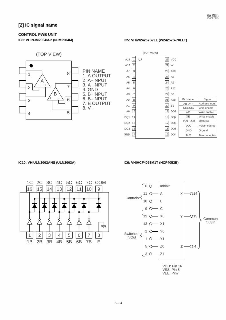
UX-108HUX-178H
8 – 4
[2] IC signal name
CONTROL PWB UNITIC9: VHiNJM2904M-2 (NJM2904M)
IC10: VHiULN2003ANS (ULN2003A)
IC5: VHiW24257S7LL (W24257S-70LLT)
IC6: VHiHCF4053M1T (HCF4053B)
–+
– +
1 8 PIN NAME 1. A OUTPUT 2 .A–INPUT 3. A+INPUT 4. GND 5. B+INPUT 6. B–INPUT 7. B OUTPUT 8. V+
(TOP VIEW)
3 6
2 7
4 5
B
A
16 15 14 13 12 11 10 9
1 2 3 4 5 6 7 81B 2B 3B 4B 5B 6B 7B E
1C 2C 3C 4C 5C 6C 7C COM
Signal
A0~A12CE1/CE2
WE
OE
I/O1~I/O8
VCC
GND
N.C.
Address input
Chip enable
Write enable
Write enable
Data I/O
Power source
Ground
No connection
1
2
3
4
5
6
7
8
9
10
11
12
13
14
A14
A12
A7
A6
A5
A4
A3
A2
A1
A0
DQ1
DQ2
DQ3
GND
28
27
26
25
24
23
22
21
20
19
18
17
DQ5
DQ6
DQ7
DQ8
S1
A10
S2
A11
A9
A8
A13
W
VCC
(TOP VIEW)
16
15 DQ4
Pin name
6
11
10
9
12
13
2
1
Inhibit
Controls14
15Common
Out/In
5
Switches In/Out
4
3
A
B
C
X0
X1
Y0
Y1
Z0
Z1
X
Y
Z
VDD: Pin 16 VSS: Pin 8 VEE: Pin7

UX-108HUX-178H
8 – 5
IC8: VHiNJM2902M-1 (NJM2902)
IC3: VHiHCF4066M1T (HCF4066)
IC100: VHiPST596CMT1 (PST596CNR)
IC7: VHi27C01012TI (27C010)EP-ROM
IC1: VHiMC34119DR2 (MC34119DR2)
+–
1
A+ –
D2
3
4
14
13
12
11
5
6
7
10
9
8
+–B
+ –C
D OUTPUT
D-INPUT
D+INPUT
GND
C+INPUT
C-INPUT
C OUTPUTB OUTPUT
B-INPUT
B+INPUT
V+
A+INPUT
A-INPUT
A OUTPUT
1
3
5
7
14
12
10
8
IN/OUT
OUT/IN
CONT. B
VDD
CONT. D
OUT/IN
IN/OUT
2OUT/IN
4IN/OUT
6CONT. C
13
11
9
CONT. A
IN/OUT
OUT/IN
VCC
OUT/IN IN/OUTSWA
OUT/IN IN/OUT
SWD
IN/OUT OUT/INSWB
IN/OUT OUT/INSWC
1
2
M/R
SUB
5 VCC
(TOP VIEW)
3GND 4 VOUT
1
2
3
4
5
6
7
8
9
10
11
12
13
VPP
A16
A15
A12
A7
A6
A5
A4
A3
A2
A1
A0
DQ1
32
31
30
29
28
27
26
25
24
23
22
21
20
VCC
PGM
NC
A14
A13
A8
A9
A11
G
A10
E
DQ8
DQ7
14
15
16
DQ2
DQ3
GND
DQ6
DQ5
DQ4
19
18
17
(TOP VIEW)
Pin name
A0~A16
E
G
GND
PGM
DQ1~DQ8
VCC
VPP
Signal
Address input
Chip enable
Output enable
Ground
Program
Data output (Program input)
+5V power
+12.5V power(*)
(*) Only in the program mode
1
2
3
4
CD
FC2
FC1
VIN
8
7
6
5 VO1
VCC
GND
VO2
(TOP VIEW)

UX-108HUX-178H
8 – 6
IC4: VHiR96XFC3CID (96DFXL-CID)
SWGAINI
0VD1
+5VD2
0VA
NC
NC
RAMPIN
0VA
0VD2
D0
D1
D2
D3
D4
D5
D6
GP
02
SW
GA
INO
RC
VO
0VD
2
RLS
Dn
RX
D
GP
19
GP
20
0VD
2
GP
21
EY
EY
0VD
2
DA
OU
T
AD
IN
EY
EX
EY
EC
LK
NC
NC
NC
DA
IN
AD
OU
T
BY
PA
SS
RC
VI
TX
LOS
S3
TX
LOS
S2
TX
LOS
S1
NC
NC
0VA
TX
OU
T
RX
IN
+5V
A
RS3
RS2
RS1
RS0
GP13
SEE NOTE 1
GP11
RTSn
EN85n
0VD2
PORin
XTLI
XTLO
XCLK
YCLK
+5VD1
24
100
99 98 97 96 95 94 93 92 91 90 89 88 87 86 85
31 32 33 34 35 36 37 38 39 40 41 42 43 44 45 46
57
58
59
60
61
62
63
64
65
66
67
68
69
70
71
72
23
22
21
20
19
18
17
16
15
14
13
12
11
10
9
8
7
6
5
4
3
2
1
D7
0VD2
0VD2
GP07
GP06
GP05
GP04
GP03
DCLKI(IRQ2n)73
SYNCIN2(G2XCLK)74
GP1675
GP1776
0VD277
CTSn78
TXD79
0VD280
ECLKIN1 25
SYNCIN1 26
NC 27
NC 28
NC 29
0VA 30
0VA
47
AG
D48
AO
UT
49
0VD
150
RS456
READn55
CSn54
WRITEn53
IRQn52
NC51
EY
EC
LKX
84
EY
ES
YN
C83
DC
LK82
0VD
281
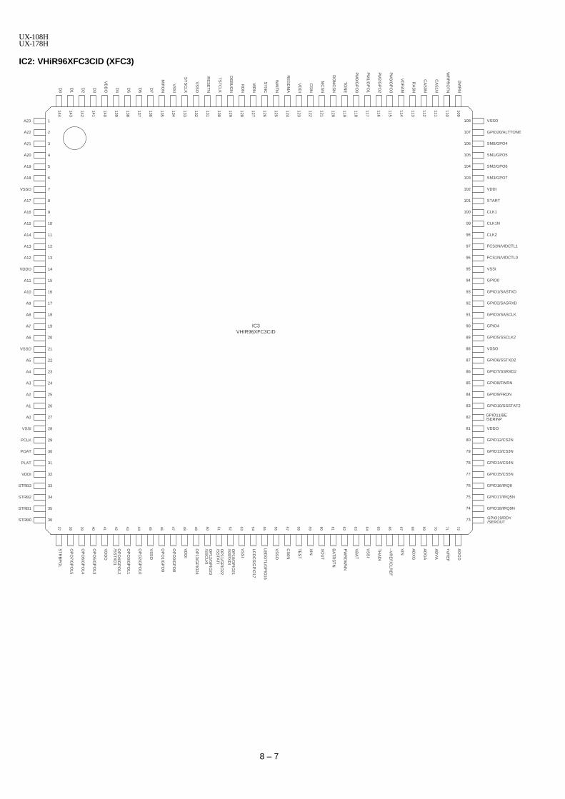
UX-108HUX-178H
8 – 7
IC2: VHiR96XFC3CID (XFC3)
ST
RB
PO
L37
A23 1
A22 2
A21 3
A20 4
A19 5
A18 6
VSSO 7
A17 8
A16 9
A15 10
A14 11
A13 12
A12 13
VDDO 14
A11 15
A10 16
A9 17
A8 18
A7 19
A6 20
VSSO 21
A5 22
A4 23
A3 24
A2 25
A1 26
A0 27
VSSI 28
PCLK 29
POAT 30
VSSO108
GPIO20/ALTTONE107
106
105
104
SM3/GPO7103
VDDI102
START101
CLK1100
CLK1N99
CLK298
97
FCS1N/VIDCTL096
VSSI95
94
93
92
91
90
89
88
87
86
85
84
83
82
VDDO81
80
79
D0
144
D1
143
D2
142
D3
141
VD
DO
140
D4
139
138
137
136
135
134
133
132
131
130
DE
BU
GN
129
RD
N128
WR
N127
126
109
D6
D7
SY
SC
LK
VS
SO
RE
SE
TN
TS
TC
LK
SY
NC
DW
RND5
MIR
ON
VS
SI
OP
O7/G
PO
1538
OP
O6/G
PO
1439
OP
O5/G
PO
1340
VD
DO
41
OP
O4/G
PO
12 /S
ST
XD
142
OP
O3/G
PO
1143 44
VS
SO
45 46 47
VD
DI
48 49 50 51 52
VS
SI
53
VS
SO
72
LCD
CS
/GP
IO17
54 55
RE
GD
MA
124
VD
DI
123
122
121
120
119
118
117
116
115
114
RA
SN
113
CA
S0N
112
CA
S1N
111
110
125
MC
SN
RO
MC
SN
PM
3/GP
O3
VD
RA
M
WR
PR
OT
N
WA
ITN
CS
IN
TO
NE
CS
0N57
TE
ST
58
XIN
59
XO
UT
60
BA
TR
ST
N61
PW
RD
WN
N62
VB
AT
63
VS
SI
64
TH
AD
I65
–VR
EF
/CLR
EF
66
VIN
67
AD
XG
68
AD
GA
69
AD
GD
56
AD
VA
70
+V
RE
F71
PLAT 31
VDDI 32
STRB3 33
STRB2 34
STRB1 35
STRB0 36
78
77
76
75
GPIO18/IRQ9N74
GPIO19/RDY /SEROUT73
OP
O2/G
PO
10
OP
O1/G
PO
9
OP
O0/G
PO
8
OP
13/GP
IO24
OP
12/GP
IO23
/SS
CLK
I
OP
11/GP
IO22
/SS
TA
TI
OP
10/GP
IO21
/SS
RX
DI
LED
GT
L/GP
IO16
GPIO17/IRQ5N
GPIO16/IRQ8
GPIO15/CS5N
GPIO14/CS4N
GPIO13/CS3N
GPIO12/CS2N
GPIO11/BE /SERINP
GPIO10/SSSTAT2
GPIO9/FRDN
GPIO8/FWRN
GPIO7/SSRXD2
GPIO6/SSTXD2
VSSO
GPIO5/SSCLK2
GPIO4
GPIO3/SASCLK
GPIO2/SASRXD
GPIO1/SASTXD
GPIO0
FCS2N/VIDCTL1
SM2/GPO6
SM1/GPO5
SM0/GPO4
PM
2/GP
O2
PM
1/GP
O1
PM
0/GP
O0
IC3 VHIR96XFC3CID

1 - 1
UX-108HUX-178H
CONTENTS
PARTS GUIDE
Because parts marked with " " is indispensable for the machine safety maintenance and operation, it must bereplaced with the parts specifi to the product specification.
1 Cabinet, etc.
2 Upper cabinet
3 Document guide upper
4 Drive unit (Non cutter model)(UX-108)
5 Drive unit (Cutter model)(UX-178)
6 Packing material & Accessories
7 Control PWB unit
8 TEL-Liu PWB unit
9 Power supply PWB unit
50 Hardware parts
Index
UX-108MODEL UX-178Non Cutter model Cutter model
UX-108 UX-178
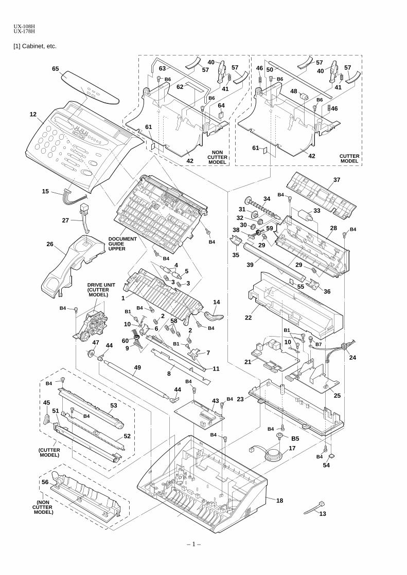
UX-108HUX-178H
[1] Cabinet, etc.
– 1 –
57 57
12
40
41
63
B6
B6
B4
B1
B7
B4
B4
B5
B4
B4
B4
B1
B1
B4
B4
B4
42
37
33
28
34
3132
3038
35
39
29
29
22
24
5536
2523
54
21
10
17
13
43
18
8
47 44
44
49
9
610
258
2
7
11
141
54
3 3
26
27
B4
B4
64
15
DOCUMENTGUIDEUPPER
60
61
62
59
575740
41
46
46
50B6
B6
48
4261
CUTTERMODEL
NONCUTTERMODEL
B4
B4
56
4551
52
53
(NONCUTTER MODEL)
(CUTTER MODEL)
B4
DRIVE UNIT(CUTTER MODEL)
65

UX-108HUX-178H
NO. PARTS CODEPRICERANK
NEWMARK
PARTRANK
DESCRIPTION
– 2 –
[1] Cabinet etc.1 LFRM-2184XHZZ AP N C Head frame2 MSPRC2949FFZZ AA N C Head spring A3 MSPRC2950FFZZ AA N C Pinch roller pressing spring4 NROLP2334XHZA AC N C Pinch roller5 NSFTZ2281FFZZ AB N C Pinch roller shaft6 PGIDP2497XHZZ AC N C Head support,left7 PGIDP2498XHZZ AC N C Head support,right8 PSHEZ3324FFZZ AA N C Head sheet9 QCNW-4748XHZA AH N C Head cable
10 QCNW-4754XHZZ AA N C Head earth cable11 RHEDZ2054XHZZ BP N B Thermal head12 DCEKP378BFF02 BG N E Operation panel unit13 LHLDW1033CE00 AA C Band14 LSTPF2049XHZZ AD N C Stopper plate15 QCNW-4816XHZA AG N C Panel cable17 CCNW-4745FF01 AG N C Speaker ass’y18 GCABB2298FFZA AL N D Lower cabinet19 MLEVP2263XHZZ AC N C Paper sensor lever [178H]20 MSPRD2947FFZZ AB N C Paper sensor lever spring [178H]21 DCEKL376BFFHS BL N E TEL/Liu PWB unit22 GCASP2099FFZZ AH N C PWB case,top23 GCASP2100FFZZ AG N C PWB case,bottom
! 24 QACCB2014FFZZ AT B AC cord ass’y! 25 RDENT2121XHZZ BG N E Power supply PWB unit
26 GDAI-2078FFZA AE N C Handset cover27 MLEVP2261XHZZ AD N C Hook switch lever28 LFRM-2185XHZZ AH N C Scanner fram29 MSPRC2948FFZZ AA N C CIS spring30 NGERH2379XHZZ AC N C Idler gear,25Z31 NGERH2380XHZZ AC N C Reduction gear,17/36Z32 NGERH2392XHZZ AC N C Reduction gear,17/21Z33 NROLR2375XHZZ AL N C Feed roller34 NSFTZ2273XHZZ AF N C Feed roller shaft35 PGIDP2499XHZZ AD N C CIS support,left [108H]
PGIDP2513XHZZ AH N C CIS support,left [178H]36 PGIDP2500XHZZ AD N C CIS support,right [108H]
PGIDP2514XHZZ AH N C CIS support,right [178H]37 PGIDP2505XHZZ AF N C Document guide lower38 QCNW-4747XHZZ AH N C CIS cable [108H]
QCNW-4814XHZZ AG N C CIS cable [178H]39 RUNTZ2020SCZZ BF N B CIS unit [108H]
RUNTZ2021SCZZ BF N B CIS unit [178H]40 MLEVP2262XHZZ AD N C Paper sensor lever41 MSPRC2989FFZZ AA N C Paper sensor lever spring42 PGIDP2496XHZZ AD N C Paper support guide43 DCEKC780JFFHS BQ N E Control PWB unit(Within ROM) [108H]
DCEKC989JFFHS BQ N E Control PWB unit(Within ROM) [178H]44 LBSHP2092XHZZ AC N C Platen bearing45 MARMP2019XHZZ AC N C Cutter arm [178H]46 MSPRC2945FFZZ AA N C Anti curl spring [178H]47 NGERH2382XHZZ AC N C Platen gear48 NROLP2332XHZZ AD C PO pinch roller [178H]49 NROLR2376XHZZ AX N C Platen roller50 NSFTZ2274FFZZ AD N C Anti curl shaft [178H]51 PCUT-2037SCZZ AT N C Cutter [178H]52 PGIDP2506XHZZ AE N C Cuter guide [178H]53 PGIDP2507XHZZ AF N C Cutter cover [178H]54 GLEGG2068FFZZ AA N C Rubber leg55 PSHEZ3116FFCG AB N C Jack sheet56 PGIDP2503XHZZ AD N C Paper guide upper [108H]57 PSHEZ3374XHZZ AC N C Guide sheet(D) [108H]
PSHEZ3362XHZZ AD N C Guide sheet [178H]58 MSPRC3005FFZZ AA N C Head spring B
! 59 RCORF2063XHZZ AF B Core! 60 RCORF2064XHZZ AF B Core
61 PSHEZ3364FFZZ AB N C Sensor sheet62 TLABH4593FFZZ AB N D Paper set label [108H]63 PWIR-2029FFZZ AF N C Guide wire [108H]64 PSHEZ3369FFZZ AA N C Guide wire sheet [108H]65 HPNLH2383FFZB AG N C Decoration panel [108H]
HPNLH2383FFZE AG N C Decoration panel [178H]

UX-108HUX-178H
– 3 –
[2] Upper cabinet
[3] Document guide upper
3 2
75
6
4
915
10
16
1
14
13
12
1
11
8
17
14
2
1
3
5
4
12
10
8
7
9
6
B2
B3
B3
13

UX-108HUX-178H
NO. PARTS CODEPRICERANK
NEWMARK
PARTRANK
DESCRIPTION
– 4 –
[2] Upper cabinet1 GCABA2297XHZE AM N D Upper cabinet2 JBTN-2216XHZA AF N C 12 key3 JBTN-2217XHZA AD N C Direct key4 JBTN-2218XHZZ AE N C Start key5 JBTN-2219XHZZ AD N C Stop key6 LPLTP2909XHZA AE N C Document tray7 MSPRC2954XHZZ AC N C Hopper spring8 NGERP2318XHZZ AD C Pinion gear9 PGIDP2501XHZA AE N C Hopper guide,left
10 PGIDP2502XHZA AE N C Hopper guide,right12 QCNW-4816XHZA AG N C Panel cable13 DCEKP367BXH01 BH N E Operation panel PWB unit14 LBNDJ2006XHZZ AA C Band(100mm)
(Unit)901 DCEKP378BFF02 BG N E Operation panel unit
[3] Document guide upper1 LBSHP2093XHZZ AC N C Bearing2 LPLTG2911XHZZ AE N C Separator rubber3 LPLTP2908XHZZ AE N C Separator plate4 MLEVP2264XHZZ AD N C Panel lock lever5 MLEVP2265XHZZ AD N C Document sensor lever6 MSPRD2953XHZZ AC N C Document sensor lever spring7 MSPRP2944XHZZ AC N C Paper feed spring8 MSPRT2951XHZZ AC N C Separate spring9 MSPRT2951XHZZ AC N C Panel lock lever spring
10 NGERH2383XHZZ AC N C Idler gear,2011 NGERH2402XHZZ AC N C CIS gear,29Z12 NROLR2387XHZZ AZ N C CIS roller A ass’y13 NROLR2388XHZZ AZ N C CIS roller B ass’y14 NROLR2374XHZZ AP N C Transfer roller15 PGIDP2504XHZZ AF N C Document guide upper16 PSHEZ3355XHZZ AD N C Rear sheet17 NGERH2405SCZZ AD N C Cuppling gear

UX-108HUX-178H
– 5 –
[4] Drive unit (Non cutter model)(UX-108)
[5] Drive unit (Cutter model)(UX-178)
19
2
1
16
18
1213
1213
11
9
6
3
114
85
8
13
B4
19
2
17
18
1
16
18
1213
14
11 15 1213
138 7
1511
9
6
3
11
10
4
85
8
13
B4

UX-108HUX-178H
NO. PARTS CODEPRICERANK
NEWMARK
PARTRANK
DESCRIPTION
– 6 –
[4] Drive unit(Non cutter model)(UX-108H)1 LFRM-2187XHZZ AR N C Drive unit frame2 LPLTM2910XHZZ AE N C Motor heat sink3 MCAMP2024XHZZ AE N C Cam4 MLEVP2266XHZZ AD N C Planet gear lever A5 MLEVP2267XHZZ AD N C Planet gear lever B6 MLEVP2268XHZZ AD N C Change lever A8 MSPRC2955XHZZ AC N C Planet gear spring9 MSPRT2956XHZZ AC N C Change lever spring
11 NGERH2379XHZZ AC N C Idler gear 25Z12 NGERH2380XHZZ AC N C Reduction gear 17/36Z13 NGERH2387XHZZ AC N C Planet gear 17Z16 QCNW-4749XHZZ AD N C Cam switch cable18 QSW-F2224SCZZ AE B Detection switch19 RMOTZ2134XHZZ BA N B Motor
[5] Drive unit(Cutter model)(UX-178H)1 LFRM-2186XHZZ AH N C Drive unit frame2 LPLTM2910XHZZ AE N C Motor heat sink3 MCAMP2024XHZZ AE N C Cam4 MLEVP2266XHZZ AD N C Planet gear lever A5 MLEVP2267XHZZ AD N C Planet gear lever B6 MLEVP2268XHZZ AD N C Change lever A7 MLEVP2270XHZZ AD N C Planet gear lever C8 MSPRC2955XHZZ AC N C Planet gear spring9 MSPRT2956XHZZ AC N C Change lever spring
10 NGERH2356XHZZ AC N C Idler gear,20Z11 NGERH2379XHZZ AC N C Idler gear,25Z12 NGERH2380XHZZ AC N C Reduction gear,17/36Z13 NGERH2387XHZZ AC N C Planet gear,17Z14 NGERH2390XHZZ AC N C Cutter gear,44Z15 NGERH2391XHZZ AC N C Reduction gear,17/30Z16 QCNW-4749XHZZ AD N C Cam switch cable17 QCNW-4750XHZZ AD N C Cutter cam switch cable18 QSW-F2224SCZZ AE B Detection switch19 RMOTZ2134XHZZ BA N B Motor

UX-108HUX-178H
– 7 –
[6] Packing material & Accessories
2
10
8
3
11
67
9
5
FAXPAPER
1
ACCORD
13
23
TAPE
TAPE
16
20
21
1719
1822
CUTTER ARM
[6] Packing material & Accessories1 TINSE3782FFZZ AD N D Operation manual2 TLABH4344FFZZ AC N D Rapid key labels3 SPAKC242AFFZZ AH N D Packing case [108H]
SPAKC272AFFZZ AH N D Packing case [178H]5 DUNTK369BFFSG AM N E Handset6 QCNW-4650FFZZ AH C Telephone line cord7 QCNW-3976XHAG AH C Handset cord8 SPAKP3385FFZZ AB D Vinyl cover9 SPAKA231AFFZZ AB N D Pad
10 SPAKA161AFFZL AF N D Packing add.,left11 SPAKA162AFFZR AF N D Packing add.,right13 PCUSK2113FFZZ AA N C CIS pad16 TLABM4518FFZZ AD N D Pop label [108H]
TLABM4524FFZZ AF N D Pop label [178H]17 TCADZ2306FFZA AC N D After card18 TCADZ2323FFUX AC N D Warranty card19 TLABZ3077FFZB AB N D Service call card20 QCNW-4266FFZZ AF C UK jack cable21 TLABZ2549FFZZ AB N D Emergency label22 TCADZ2623FFZZ AA N D Errata sheet23 PCUSK2115FFZZ N C Cutter pad [178H]
NO. PARTS CODEPRICERANK
NEWMARK
PARTRANK
DESCRIPTION
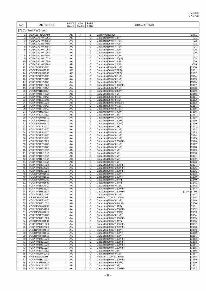
UX-108HUX-178H
NO. PARTS CODEPRICERANK
NEWMARK
PARTRANK
DESCRIPTION
– 8 –
[7] Control PWB unit1 UBATZ6441CCMM AE N B Battery(CR2032) [BAT1]2 VCEAGA1HW105M AB C Capacitor(50WV 1µF) [C1]3 VCEAGA1HW475M AA C Capacitor(50WV 4.7µF) [C2]4 VCEAGA1EW476M AA C Capacitor(25WV 47µF) [C3]5 VCEAGA1HW475M AA C Capacitor(50WV 4.7µF) [C4]6 VCEAGA1HW106M AA C Capacitor(50WV 10µF) [C5]7 VCEAGA1HW106M AA C Capacitor(50WV 10µF) [C6]8 VCEAGA1EW476M AA C Capacitor(25WV 47µF) [C7]9 VCEAGA1HW107M AA C Capacitor(50WV 100µF) [C8]
10 VCEAGA1HW106M AA C Capacitor(50WV 10µF) [C9]11 VCEAGA1HW226M AB C Capacitor(50WV 22µF) [C10]12 VCKYTV1EF104Z AA C Capacitor(25WV 0.1µF) [C100]13 VCCCTV1HH270J AC C Capacitor(50WV 27PF) [C101]14 VCCCTV1HH270J AC C Capacitor(50WV 27PF) [C102]15 VCKYTV1EF104Z AA C Capacitor(25WV 0.1µF) [C104]16 VCKYTV1EF104Z AA C Capacitor(25WV 0.1µF) [C105]17 VCKYTV1EF104Z AA C Capacitor(25WV 0.1µF) [C106]18 VCKYTV1HB102K AA C Capacitor(50WV 1000PF) [C107]19 VCKYTV1EF104Z AA C Capacitor(25WV 0.1µF) [C108]20 VCCSTV1HL331J AA C Capacitor(50WV 330PF) [C109]21 VCKYTV1CF105Z AB C Capacitor(16WV 1µF) [C110]22 VCKYTV1EF104Z AA C Capacitor(25WV 0.1µF) [C111]23 VCKYTV1EB104K AA C Capacitor(25WV 0.1µF) [C112]24 VCKYTV1HB103K AB C Capacitor(50WV 0.01µF) [C113]25 VCKYTV1EF104Z AA C Capacitor(25WV 0.1µF) [C114]26 VCKYTV1EF104Z AA C Capacitor(25WV 0.1µF) [C115]27 VCCSTV1HL391J AA C Capacitor(50WV 390PF) [C116]28 VCKYTV1CF105Z AB C Capacitor(16WV 1µF) [C117]29 VCCCTV1HH101J AA C Capacitor(50WV 100PF) [C118]30 VCCCTV1HH101J AA C Capacitor(50WV 100PF) [C119]31 VCCCTV1HH101J AA C Capacitor(50WV 100PF) [C120]32 VCKYTV1CF105Z AB C Capacitor(16WV 1µF) [C121]33 VCKYTV1EF104Z AA C Capacitor(25WV 0.1µF) [C122]34 VCKYTV1EF104Z AA C Capacitor(25WV 0.1µF) [C123]35 VCKYTV1EF104Z AA C Capacitor(25WV 0.1µF) [C124]36 VCKYTV1EF104Z AA C Capacitor(25WV 0.1µF) [C125]37 VCKYTV1HB222K AA C Capacitor(50WV 2200PF) [C126]38 VCKYTV1EF104Z AA C Capacitor(25WV 0.1µF) [C127]39 VCKYTV1EF104Z AA C Capacitor(25WV 0.1µF) [C128]40 VCKYTV1CF105Z AB C Capacitor(16WV 1µF) [C129]41 VCKYTV1CF105Z AB C Capacitor(16WV 1µF) [C130]42 VCKYTV1CF105Z AB C Capacitor(16WV 1µF) [C131]43 VCKYTV1CF105Z AB C Capacitor(16WV 1µF) [C132]44 VCKYTV1CF105Z AB C Capacitor(16WV 1µF) [C133]45 VCKYTV1HB102K AA C Capacitor(50WV 1000PF) [C134]46 VCKYTV1HB222K AA C Capacitor(50WV 2200PF) [C135]47 VCKYTV1HB102K AA C Capacitor(50WV 1000PF) [C136]48 VCCCTV1HH101J AA C Capacitor(50WV 100PF) [C138]49 VCCCTV1HH101J AA C Capacitor(50WV 100PF) [C139]50 VCCCTV1HH220J AA C Capacitor(50WV 22PF) [C140]51 VCCCTV1HH150J AA C Capacitor(50WV 15PF) [C141]52 VCKYTV1EF104Z AA C Capacitor(25WV 0.1µF) [C142]53 VCKYTV1HB222K AA C Capacitor(50WV 2200PF) [C143]54 VCKYTV1HB222K AA C Capacitor(50WV 2200PF) [C144][178H]55 VCKYTV1EB104K AA C Capacitor(25WV 0.1µF) [C147]56 VRS-TS2AD000J AA C Resistor(1/10W 0Ω ±5%) [C148]57 VCKYTV1EF104Z AA C Capacitor(25WV 0.1µF) [C149]58 VCKYTV1HB103K AB C Capacitor(50WV 0.01µF) [C150]59 VCCCTV1HH180J AA C Capacitor(50WV 18PF) [C151]60 VCKYTV1HB472K AA C Capacitor(50WV 4700PF) [C152]61 VCCCTV1HH101J AA C Capacitor(50WV 100PF) [C153]62 VCKYTV1EF104Z AA C Capacitor(25WV 0.1µF) [C154]63 VCKYTV1HB102K AA C Capacitor(50WV 1000PF) [C155]64 VCCCTV1HH180J AA C Capacitor(50WV 18PF) [C156]65 VCKYTV1HB102K AA C Capacitor(50WV 1000PF) [C157]66 VCKYTV1HB222K AA C Capacitor(50WV 2200PF) [C158]67 VCCCTV1HH101J AA C Capacitor(50WV 100PF) [C159]68 VCCCTV1HH101J AA C Capacitor(50WV 100PF) [C160]69 VCCCTV1HH101J AA C Capacitor(50WV 100PF) [C161]70 VCKYTV1HB102K AA C Capacitor(50WV 1000PF) [C162]71 VCKYTV1HB102K AA C Capacitor(50WV 1000PF) [C163]72 VCKYTV1HB102K AA C Capacitor(50WV 1000PF) [C164]73 VCKYTV1HB102K AA C Capacitor(50WV 1000PF) [C165]74 VCKYTV1CF105Z AB C Capacitor(16WV 1µF) [C166]75 VCKYTQ1HF104Z AA C Capacitor(50WV 0.1µF) [C167]76 VRS-TS2AD000J AA C Resistor(1/10W 0Ω ±5%) [C168]77 VCCSTV1HL102J AA C Capacitor(50WV 1000PF) [C169]78 VCKYTV1HB681K AA C Capacitor(50WV 680PF) [C170]79 VCKYTV1CF105Z AB C Capacitor(16WV 1µF) [C171]80 VCKYTV1HB222K AA C Capacitor(50WV 2200PF) [C172]

UX-108HUX-178H
NO. PARTS CODEPRICERANK
NEWMARK
PARTRANK
DESCRIPTION
– 9 –
[7] Control PWB unit81 VCKYTV1HB102K AA C Capacitor(50WV 1000PF) [C173]82 VCKYTV1HB102K AA C Capacitor(50WV 1000PF) [C176]83 VCKYTV1HB102K AA C Capacitor(50WV 1000PF) [C177]84 VCKYTV1EF104Z AA C Capacitor(25WV 0.1µF) [C178]85 VCKYTV1HB102K AA C Capacitor(50WV 1000PF) [C179]86 VCKYTV1HB102K AA C Capacitor(50WV 1000PF) [C180]87 VCCCTV1HH220J AA C Capacitor(50WV 22PF) [C181]88 VCKYTV1HB102K AA C Capacitor(50WV 1000PF) [C182]89 VCKYTV1EF104Z AA C Capacitor(25WV 0.1µF) [C183]90 VCCCTV1HH820J AA C Capacitor(50WV 82PF) [C184]91 VCCCTV1HH820J AA C Capacitor(50WV 82PF) [C185]92 VCCCTV1HH820J AA C Capacitor(50WV 82PF) [C186]93 VCCCTV1HH820J AA C Capacitor(50WV 82PF) [C187]94 VCCCTV1HH820J AA C Capacitor(50WV 82PF) [C188]95 VCCCTV1HH820J AA C Capacitor(50WV 82PF) [C190]96 VCCCTV1HH820J AA C Capacitor(50WV 82PF) [C191]97 VCCCTV1HH820J AA C Capacitor(50WV 82PF) [C192]98 VCCCTV1HH820J AA C Capacitor(50WV 82PF) [C193]99 VCKYTV1EF104Z AA C Capacitor(25WV 0.1µF) [C194]
100 VCKYTV1EF104Z AA C Capacitor(25WV 0.1µF) [C195]101 VCCCTV1HH820J AA C Capacitor(50WV 82PF) [C196]102 VCKYTV1HB102K AA C Capacitor(50WV 1000PF) [C197]103 VCKYTV1HB102K AA C Capacitor(50WV 1000PF) [C199]104 VCKYTV1HB102K AA C Capacitor(50WV 1000PF) [C200]105 VCKYTV1EF104Z AA C Capacitor(25WV 0.1µF) [C203]106 VCKYTV1EF104Z AA C Capacitor(25WV 0.1µF) [C204]107 VCKYTV1HB102K AA C Capacitor(50WV 1000PF) [C205]108 VCKYTV1HB102K AA C Capacitor(50WV 1000PF) [C206]109 VCKYTQ1HF104Z AA C Capacitor(50WV 0.1µF) [C207]110 VCKYTV1HB102K AA C Capacitor(50WV 1000PF) [C208]111 VCKYTV1HB102K AA C Capacitor(50WV 1000PF) [C209]112 VCKYTV1HB102K AA C Capacitor(50WV 1000PF) [C210]113 VCKYTV1EF104Z AA C Capacitor(25WV 0.1µF) [C211]114 VCKYTV1HB102K AA C Capacitor(50WV 1000PF) [C212]115 VCKYTV1HB102K AA C Capacitor(50WV 1000PF) [C213]116 QCNCM7014SC0G AB C Connector(7pin) [CNCIS]117 QCNCM2442SC0B AB C Conector(2pin) [CNCSW]118 QCNCM7014SC0B AD C Conector(2pin) [CNCUT1][178H]119 QCNCW2500SC1J AD N C Connector(10Pin) [CNLIUA]120 QCNCW2500SC0F AE N C Connector(6pin) [CNLIUB]121 QCNCM7014SC0F AB C Connector(6pin) [CNMT]122 QCNCM7014SC1E AC C Connector(15pin) [CNPN]123 QCNCW2500SC1J AD N C Connector(10pin) [CNPW]124 QCNCM2401SC0B AA C Connector(2pin) [CNSP]125 QCNCM7014SC1F AD C Connector(16pin) [CNTH]126 VHEMPZP4748A1 AA N B Zener diode(MPZP4748) [D1]127 VHD1SS355//-1 AB B Diode(1SS355) [D100]128 VHDRB705D//-1 AD B Diode(RB705D) [D101]129 VHVICPS07//-1 AA B Varistor(ICP-S07) [FU100]130 VHIMC34119DR2 AH B IC(MC34119DR2) [IC1]131 VHIR96XFC3CID BR N B IC(XFC3) [IC2][Within IC2 and IC4 pair]132 VHIHCF4066M1T AF N B IC(HCF4066M) [IC3]133 VHIR96XFC3CID BR N B IC(R96DFXL-CID) [IC4][Within IC2 and IC4 pair]134 VHIW24257S7LL AP N B IC(W24257S-70LLT) [IC5]135 VHIHCF4053M1T AG N B IC(HCF4053M) [IC6]136 QSOCZ2051SC32 AC C IC socket(32pin) [IC7]
VHI27010FWV0E AY N B IC,EPROM(1M) [IC7][108H]VHI27010FXN0E AY N B IC,EPROM(1M) [IC7][178H]
138 VHINJM2902M-1 AF B IC(NJM2902M) [IC8]139 VHINJM2904M-2 AG N B IC(NJM2904M) [IC9]140 VHIULN2003ANS AE B IC(ULN2003ANS) [IC10]141 VHIPST596CMT1 AF B IC(PST596CNR) [IC100]142 VRS-TS2AD271J AA C Resistor(1/10W 270Ω ±5%) [L100]143 VRS-TS2AD000J AA C Resistor(1/10W 0Ω ±5%) [L101]144 VRS-TS2AD000J AA C Resistor(1/10W 0Ω ±5%) [L102]145 VRS-TS2AD000J AA C Resistor(1/10W 0Ω ±5%) [L103]146 RCILZ2104SCZZ AK C Coil(Z2104) [L104]147 VRS-TS2AD000J AA C Resistor(1/10W 0Ω ±5%) [L105]148 VHPITR9606/-1 AG N B Photo transistor(ITR9606) [PI1][178H]149 VS2SD1858Q2-1 AE N B Transistor(2SD1858) [Q1]150 VS2SC2412KS-1 AB B Transistor(2SC2412KS) [Q101]151 VS2SA1037KS-1 AB B Transistor(2SA1037KS) [Q102]152 VSBCR133///-1 AA N B Transistor(BCR133) [Q103][108H]153 VRS-VV3AB270J AA N C Resistor(1W 27Ω ±5%) [R1][108H]154 VRD-RC2EY100J AA C Resistor(1/4W 10Ω ±5%) [R2]155 VRS-TS2AD000J AA C Resistor(1/10W 0Ω ±5%) [R101]156 VRS-TS2AD121J AA C Resistor(1/10W 120Ω ±5%) [R102]157 VRS-TS2AD271J AA C Resistor(1/10W 270Ω ±5%) [R103]158 VRS-TS2AD101J AA C Resistor(1/10W 100Ω ±5%) [R104]159 VRS-TS2AD103J AA C Resistor(1/10W 10KΩ ±5%) [R105]

UX-108HUX-178H
NO. PARTS CODEPRICERANK
NEWMARK
PARTRANK
DESCRIPTION
– 10 –
[7] Control PWB unit160 VRS-TS2AD271J AA C Resistor(1/10W 270Ω ±5%) [R106]161 VRS-TS2AD271J AA C Resistor(1/10W 270Ω ±5%) [R107]162 VRS-TS2AD103J AA C Resistor(1/10W 10KΩ ±5%) [R108]163 VRS-TS2AD271J AA C Resistor(1/10W 270Ω ±5%) [R109]164 VRS-TS2AD271J AA C Resistor(1/10W 270Ω ±5%) [R110]165 VRS-TS2AD302J AA C Resistor(1/10W 3KΩ ±5%) [R111]166 VRS-TS2AD154J AA C Resistor(1/10W 150KΩ ±5%) [R112]167 VRSTS2AD4752F AA C Resistor(1/10W 47.5KΩ ±1%) [R113]168 VRS-TS2AD104J AA C Resistor(1/10W 100KΩ ±5%) [R114]169 VRS-TS2AD103J AA C Resistor(1/10W 10KΩ ±5%) [R115]170 VRS-TS2AD3R0J AA C Resistor(1/10W 3.0Ω ±5%) [R116]171 VRS-TS2AD103J AA C Resistor(1/10W 10KΩ ±5%) [R117]172 VRS-TS2AD103J AA C Resistor(1/10W 10KΩ ±5%) [R118]173 VRS-TS2AD201J AG C Resistor(1/10W 200Ω ±5%) [R119]174 VRS-TS2AD471J AA C Resistor(1/10W 470Ω ±5%) [R120][178H]175 VRS-TS2AD471J AA C Resistor(1/10W 470Ω ±5%) [R121]176 VRS-TS2AD471J AA C Resistor(1/10W 470Ω ±5%) [R122]177 VRS-TS2AD471J AA C Resistor(1/10W 470Ω ±5%) [R123]178 VRS-TS2AD471J AA C Resistor(1/10W 470Ω ±5%) [R124]179 VRS-TS2AD471J AA C Resistor(1/10W 470Ω ±5%) [R125][178H]180 VRS-TS2AD303J AA C Resistor(1/10W 30KΩ ±5%) [R126][178H]181 VRS-TS2AD471J AA C Resistor(1/10W 470Ω ±5%) [R127]182 VRS-TS2AD103J AA C Resistor(1/10W 10KΩ ±5%) [R128]183 VRS-TS2AD271J AA C Resistor(1/10W 270Ω ±5%) [R129]184 VRS-TS2AD271J AA C Resistor(1/10W 270Ω ±5%) [R130]185 VRS-TS2AD271J AA C Resistor(1/10W 270Ω ±5%) [R131]186 VRS-TS2AD271J AA C Resistor(1/10W 270Ω ±5%) [R132]187 VRS-TS2AD271J AA C Resistor(1/10W 270Ω ±5%) [R133]188 VRS-TS2AD271J AA C Resistor(1/10W 270Ω ±5%) [R134]189 VRS-TS2AD271J AA C Resistor(1/10W 270Ω ±5%) [R135]190 VRS-TS2AD271J AA C Resistor(1/10W 270Ω ±5%) [R136]191 VRS-TS2AD271J AA C Resistor(1/10W 270Ω ±5%) [R137]192 VRS-TS2AD271J AA C Resistor(1/10W 270Ω ±5%) [R138]193 VRS-TS2AD271J AA C Resistor(1/10W 270Ω ±5%) [R139]194 VRS-TS2AD271J AA C Resistor(1/10W 270Ω ±5%) [R140]195 VRS-TS2AD221J AA C Resistor(1/10W 220Ω ±5%) [R141][178H]196 VRS-TS2AD104J AA C Resistor(1/10W 100KΩ ±5%) [R142]197 VRS-TS2AD103J AA C Resistor(1/10W 10KΩ ±5%) [R143]198 VRS-TS2AD224J AA C Resistor(1/10W 220KΩ ±5%) [R144]199 VRS-TS2AD471J AA C Resistor(1/10W 470Ω ±5%) [R145]200 VRS-TS2AD471J AA C Resistor(1/10W 470Ω ±5%) [R146]201 VRS-TS2AD103J AA C Resistor(1/10W 10KΩ ±5%) [R147]202 VRS-TS2AD303J AA C Resistor(1/10W 30KΩ ±5%) [R148]203 VRS-TS2AD000J AA C Resistor(1/10W 0Ω ±5%) [R149]204 VRS-TS2AD000J AA C Resistor(1/10W 0Ω ±5%) [R150]205 VRS-TS2AD103J AA C Resistor(1/10W 10KΩ ±5%) [R151]206 VRS-TS2AD100J AA C Resistor(1/10W 10.0Ω ±5%) [R152]207 VRS-TS2AD000J AA C Resistor(1/10W 0Ω ±5%) [R153]208 VRS-TS2AD100J AA C Resistor(1/10W 10.0Ω ±5%) [R154]209 VRS-TS2AD471J AA C Resistor(1/10W 470Ω ±5%) [R155]210 VRS-TS2AD471J AA C Resistor(1/10W 470Ω ±5%) [R156]211 VRS-TS2AD471J AA C Resistor(1/10W 470Ω ±5%) [R157]212 VRS-TS2AD471J AA C Resistor(1/10W 470Ω ±5%) [R158]213 VRS-TS2AD471J AA C Resistor(1/10W 470Ω ±5%) [R159]214 VRS-TS2AD104J AA C Resistor(1/10W 100KΩ ±5%) [R161]215 VRS-TS2AD471J AA C Resistor(1/10W 470Ω ±5%) [R162]216 VRS-TS2AD103J AA C Resistor(1/10W 10KΩ ±5%) [R163]217 VRS-TS2AD103J AA C Resistor(1/10W 10KΩ ±5%) [R164]218 VRS-TS2AD103J AA C Resistor(1/10W 10KΩ ±5%) [R165]219 VRS-TS2AD103J AA C Resistor(1/10W 10KΩ ±5%) [R166]220 VRS-TS2AD103J AA C Resistor(1/10W 10KΩ ±5%) [R167]221 VRS-TS2AD103J AA C Resistor(1/10W 10KΩ ±5%) [R168]222 VRS-TS2AD271J AA C Resistor(1/10W 270Ω ±5%) [R169]223 VRS-TS2AD271J AA C Resistor(1/10W 270Ω ±5%) [R170]224 VRS-TS2AD271J AA C Resistor(1/10W 270Ω ±5%) [R171]225 VRS-TS2AD271J AA C Resistor(1/10W 270Ω ±5%) [R172]226 VRS-TS2AD000J AA C Resistor(1/10W 0Ω ±5%) [R173]227 VRS-TS2AD271J AA C Resistor(1/10W 270Ω ±5%) [R174]228 VRS-TS2AD271J AA C Resistor(1/10W 270Ω ±5%) [R175]229 VRS-TS2AD102J AA C Resistor(1/10W 1KΩ ±5%) [R176]230 VRS-TS2AD000J AA C Resistor(1/10W 0Ω ±5%) [R177]231 VRS-TS2AD102J AA C Resistor(1/10W 1KΩ ±5%) [R178]232 VRS-TS2AD102J AA C Resistor(1/10W 1KΩ ±5%) [R179]233 VRS-TS2AD103J AA C Resistor(1/10W 10KΩ ±5%) [R180]234 VRS-TS2AD103J AA C Resistor(1/10W 10KΩ ±5%) [R181]235 VRS-TS2AD103J AA C Resistor(1/10W 10KΩ ±5%) [R182]236 VRS-TS2AD103J AA C Resistor(1/10W 10KΩ ±5%) [R183]237 VRS-TS2AD271J AA C Resistor(1/10W 270Ω ±5%) [R184]238 VRS-TS2AD271J AA C Resistor(1/10W 270Ω ±5%) [R185]239 VRS-TS2AD106J AA C Resistor(1/10W 10MΩ ±5%) [R186]
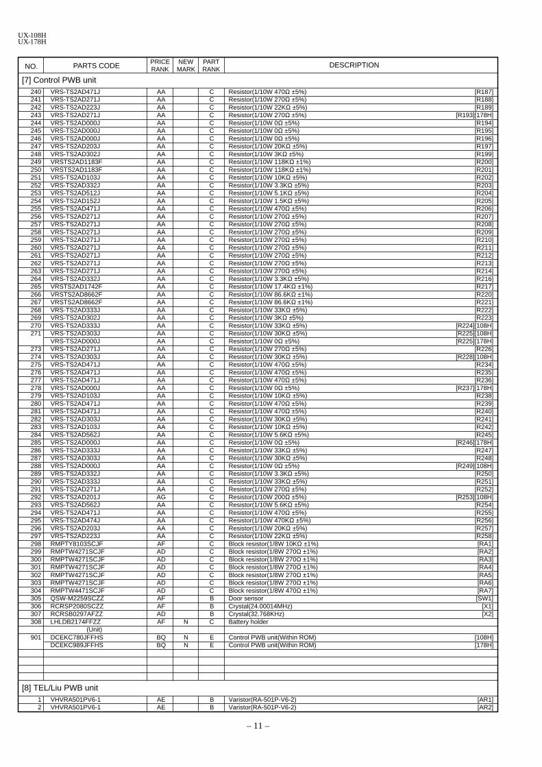
UX-108HUX-178H
NO. PARTS CODEPRICERANK
NEWMARK
PARTRANK
DESCRIPTION
– 11 –
[7] Control PWB unit240 VRS-TS2AD471J AA C Resistor(1/10W 470Ω ±5%) [R187]241 VRS-TS2AD271J AA C Resistor(1/10W 270Ω ±5%) [R188]242 VRS-TS2AD223J AA C Resistor(1/10W 22KΩ ±5%) [R189]243 VRS-TS2AD271J AA C Resistor(1/10W 270Ω ±5%) [R193][178H]244 VRS-TS2AD000J AA C Resistor(1/10W 0Ω ±5%) [R194]245 VRS-TS2AD000J AA C Resistor(1/10W 0Ω ±5%) [R195]246 VRS-TS2AD000J AA C Resistor(1/10W 0Ω ±5%) [R196]247 VRS-TS2AD203J AA C Resistor(1/10W 20KΩ ±5%) [R197]248 VRS-TS2AD302J AA C Resistor(1/10W 3KΩ ±5%) [R199]249 VRSTS2AD1183F AA C Resistor(1/10W 118KΩ ±1%) [R200]250 VRSTS2AD1183F AA C Resistor(1/10W 118KΩ ±1%) [R201]251 VRS-TS2AD103J AA C Resistor(1/10W 10KΩ ±5%) [R202]252 VRS-TS2AD332J AA C Resistor(1/10W 3.3KΩ ±5%) [R203]253 VRS-TS2AD512J AA C Resistor(1/10W 5.1KΩ ±5%) [R204]254 VRS-TS2AD152J AA C Resistor(1/10W 1.5KΩ ±5%) [R205]255 VRS-TS2AD471J AA C Resistor(1/10W 470Ω ±5%) [R206]256 VRS-TS2AD271J AA C Resistor(1/10W 270Ω ±5%) [R207]257 VRS-TS2AD271J AA C Resistor(1/10W 270Ω ±5%) [R208]258 VRS-TS2AD271J AA C Resistor(1/10W 270Ω ±5%) [R209]259 VRS-TS2AD271J AA C Resistor(1/10W 270Ω ±5%) [R210]260 VRS-TS2AD271J AA C Resistor(1/10W 270Ω ±5%) [R211]261 VRS-TS2AD271J AA C Resistor(1/10W 270Ω ±5%) [R212]262 VRS-TS2AD271J AA C Resistor(1/10W 270Ω ±5%) [R213]263 VRS-TS2AD271J AA C Resistor(1/10W 270Ω ±5%) [R214]264 VRS-TS2AD332J AA C Resistor(1/10W 3.3KΩ ±5%) [R216]265 VRSTS2AD1742F AA C Resistor(1/10W 17.4KΩ ±1%) [R217]266 VRSTS2AD8662F AA C Resistor(1/10W 86.6KΩ ±1%) [R220]267 VRSTS2AD8662F AA C Resistor(1/10W 86.6KΩ ±1%) [R221]268 VRS-TS2AD333J AA C Resistor(1/10W 33KΩ ±5%) [R222]269 VRS-TS2AD302J AA C Resistor(1/10W 3KΩ ±5%) [R223]270 VRS-TS2AD333J AA C Resistor(1/10W 33KΩ ±5%) [R224][108H]271 VRS-TS2AD303J AA C Resistor(1/10W 30KΩ ±5%) [R225][108H]
VRS-TS2AD000J AA C Resistor(1/10W 0Ω ±5%) [R225][178H]273 VRS-TS2AD271J AA C Resistor(1/10W 270Ω ±5%) [R226]274 VRS-TS2AD303J AA C Resistor(1/10W 30KΩ ±5%) [R228][108H]275 VRS-TS2AD471J AA C Resistor(1/10W 470Ω ±5%) [R234]276 VRS-TS2AD471J AA C Resistor(1/10W 470Ω ±5%) [R235]277 VRS-TS2AD471J AA C Resistor(1/10W 470Ω ±5%) [R236]278 VRS-TS2AD000J AA C Resistor(1/10W 0Ω ±5%) [R237][178H]279 VRS-TS2AD103J AA C Resistor(1/10W 10KΩ ±5%) [R238]280 VRS-TS2AD471J AA C Resistor(1/10W 470Ω ±5%) [R239]281 VRS-TS2AD471J AA C Resistor(1/10W 470Ω ±5%) [R240]282 VRS-TS2AD303J AA C Resistor(1/10W 30KΩ ±5%) [R241]283 VRS-TS2AD103J AA C Resistor(1/10W 10KΩ ±5%) [R242]284 VRS-TS2AD562J AA C Resistor(1/10W 5.6KΩ ±5%) [R245]285 VRS-TS2AD000J AA C Resistor(1/10W 0Ω ±5%) [R246][178H]286 VRS-TS2AD333J AA C Resistor(1/10W 33KΩ ±5%) [R247]287 VRS-TS2AD303J AA C Resistor(1/10W 30KΩ ±5%) [R248]288 VRS-TS2AD000J AA C Resistor(1/10W 0Ω ±5%) [R249][108H]289 VRS-TS2AD332J AA C Resistor(1/10W 3.3KΩ ±5%) [R250]290 VRS-TS2AD333J AA C Resistor(1/10W 33KΩ ±5%) [R251]291 VRS-TS2AD271J AA C Resistor(1/10W 270Ω ±5%) [R252]292 VRS-TS2AD201J AG C Resistor(1/10W 200Ω ±5%) [R253][108H]293 VRS-TS2AD562J AA C Resistor(1/10W 5.6KΩ ±5%) [R254]294 VRS-TS2AD471J AA C Resistor(1/10W 470Ω ±5%) [R255]295 VRS-TS2AD474J AA C Resistor(1/10W 470KΩ ±5%) [R256]296 VRS-TS2AD203J AA C Resistor(1/10W 20KΩ ±5%) [R257]297 VRS-TS2AD223J AA C Resistor(1/10W 22KΩ ±5%) [R258]298 RMPTY8103SCJF AF C Block resistor(1/8W 10KΩ ±1%) [RA1]299 RMPTW4271SCJF AD C Block resistor(1/8W 270Ω ±1%) [RA2]300 RMPTW4271SCJF AD C Block resistor(1/8W 270Ω ±1%) [RA3]301 RMPTW4271SCJF AD C Block resistor(1/8W 270Ω ±1%) [RA4]302 RMPTW4271SCJF AD C Block resistor(1/8W 270Ω ±1%) [RA5]303 RMPTW4271SCJF AD C Block resistor(1/8W 270Ω ±1%) [RA6]304 RMPTW4471SCJF AD C Block resistor(1/8W 470Ω ±1%) [RA7]305 QSW-M2259SCZZ AF B Door sensor [SW1]306 RCRSP2080SCZZ AF B Crystal(24.00014MHz) [X1]307 RCRSB0297AFZZ AD B Crystal(32.768KHz) [X2]308 LHLDB2174FFZZ AF N C Battery holder
(Unit)901 DCEKC780JFFHS BQ N E Control PWB unit(Within ROM) [108H]
DCEKC989JFFHS BQ N E Control PWB unit(Within ROM) [178H]
[8] TEL/Liu PWB unit1 VHVRA501PV6-1 AE B Varistor(RA-501P-V6-2) [AR1]2 VHVRA501PV6-1 AE B Varistor(RA-501P-V6-2) [AR2]
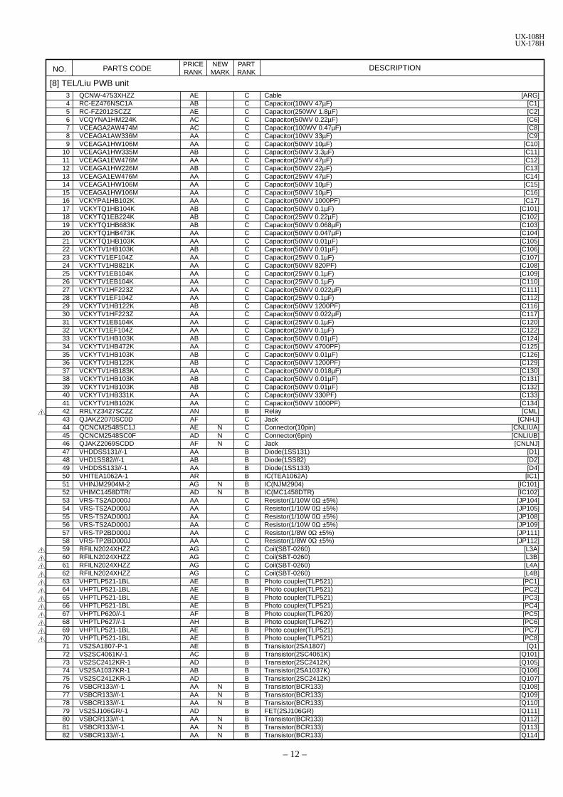
UX-108HUX-178H
NO. PARTS CODEPRICERANK
NEWMARK
PARTRANK
DESCRIPTION
– 12 –
[8] TEL/Liu PWB unit3 QCNW-4753XHZZ AE C Cable [ARG]4 RC-EZ476NSC1A AB C Capacitor(10WV 47µF) [C1]5 RC-FZ2012SCZZ AE C Capacitor(250WV 1.8µF) [C2]6 VCQYNA1HM224K AC C Capacitor(50WV 0.22µF) [C6]7 VCEAGA2AW474M AC C Capacitor(100WV 0.47µF) [C8]8 VCEAGA1AW336M AA C Capacitor(10WV 33µF) [C9]9 VCEAGA1HW106M AA C Capacitor(50WV 10µF) [C10]
10 VCEAGA1HW335M AB C Capacitor(50WV 3.3µF) [C11]11 VCEAGA1EW476M AA C Capacitor(25WV 47µF) [C12]12 VCEAGA1HW226M AB C Capacitor(50WV 22µF) [C13]13 VCEAGA1EW476M AA C Capacitor(25WV 47µF) [C14]14 VCEAGA1HW106M AA C Capacitor(50WV 10µF) [C15]15 VCEAGA1HW106M AA C Capacitor(50WV 10µF) [C16]16 VCKYPA1HB102K AA C Capacitor(50WV 1000PF) [C17]17 VCKYTQ1HB104K AB C Capacitor(50WV 0.1µF) [C101]18 VCKYTQ1EB224K AB C Capacitor(25WV 0.22µF) [C102]19 VCKYTQ1HB683K AB C Capacitor(50WV 0.068µF) [C103]20 VCKYTQ1HB473K AA C Capacitor(50WV 0.047µF) [C104]21 VCKYTQ1HB103K AA C Capacitor(50WV 0.01µF) [C105]22 VCKYTV1HB103K AB C Capacitor(50WV 0.01µF) [C106]23 VCKYTV1EF104Z AA C Capacitor(25WV 0.1µF) [C107]24 VCKYTV1HB821K AA C Capacitor(50WV 820PF) [C108]25 VCKYTV1EB104K AA C Capacitor(25WV 0.1µF) [C109]26 VCKYTV1EB104K AA C Capacitor(25WV 0.1µF) [C110]27 VCKYTV1HF223Z AA C Capacitor(50WV 0.022µF) [C111]28 VCKYTV1EF104Z AA C Capacitor(25WV 0.1µF) [C112]29 VCKYTV1HB122K AB C Capacitor(50WV 1200PF) [C116]30 VCKYTV1HF223Z AA C Capacitor(50WV 0.022µF) [C117]31 VCKYTV1EB104K AA C Capacitor(25WV 0.1µF) [C120]32 VCKYTV1EF104Z AA C Capacitor(25WV 0.1µF) [C122]33 VCKYTV1HB103K AB C Capacitor(50WV 0.01µF) [C124]34 VCKYTV1HB472K AA C Capacitor(50WV 4700PF) [C125]35 VCKYTV1HB103K AB C Capacitor(50WV 0.01µF) [C126]36 VCKYTV1HB122K AB C Capacitor(50WV 1200PF) [C129]37 VCKYTV1HB183K AA C Capacitor(50WV 0.018µF) [C130]38 VCKYTV1HB103K AB C Capacitor(50WV 0.01µF) [C131]39 VCKYTV1HB103K AB C Capacitor(50WV 0.01µF) [C132]40 VCKYTV1HB331K AA C Capacitor(50WV 330PF) [C133]41 VCKYTV1HB102K AA C Capacitor(50WV 1000PF) [C134]
! 42 RRLYZ3427SCZZ AN B Relay [CML]43 QJAKZ2070SC0D AF C Jack [CNHJ]44 QCNCM2548SC1J AE N C Connector(10pin) [CNLIUA]45 QCNCM2548SC0F AD N C Connector(6pin) [CNLIUB]46 QJAKZ2069SCDD AF N C Jack [CNLNJ]47 VHDDSS131//-1 AA B Diode(1SS131) [D1]48 VHD1SS82///-1 AB B Diode(1SS82) [D2]49 VHDDSS133//-1 AA B Diode(1SS133) [D4]50 VHITEA1062A-1 AR B IC(TEA1062A) [IC1]51 VHINJM2904M-2 AG N B IC(NJM2904) [IC101]52 VHIMC1458DTR/ AD N B IC(MC1458DTR) [IC102]53 VRS-TS2AD000J AA C Resistor(1/10W 0Ω ±5%) [JP104]54 VRS-TS2AD000J AA C Resistor(1/10W 0Ω ±5%) [JP105]55 VRS-TS2AD000J AA C Resistor(1/10W 0Ω ±5%) [JP108]56 VRS-TS2AD000J AA C Resistor(1/10W 0Ω ±5%) [JP109]57 VRS-TP2BD000J AA C Resistor(1/8W 0Ω ±5%) [JP111]58 VRS-TP2BD000J AA C Resistor(1/8W 0Ω ±5%) [JP112]
! 59 RFILN2024XHZZ AG C Coil(SBT-0260) [L3A]! 60 RFILN2024XHZZ AG C Coil(SBT-0260) [L3B]! 61 RFILN2024XHZZ AG C Coil(SBT-0260) [L4A]! 62 RFILN2024XHZZ AG C Coil(SBT-0260) [L4B]! 63 VHPTLP521-1BL AE B Photo coupler(TLP521) [PC1]! 64 VHPTLP521-1BL AE B Photo coupler(TLP521) [PC2]! 65 VHPTLP521-1BL AE B Photo coupler(TLP521) [PC3]! 66 VHPTLP521-1BL AE B Photo coupler(TLP521) [PC4]! 67 VHPTLP620//-1 AF B Photo coupler(TLP620) [PC5]! 68 VHPTLP627//-1 AH B Photo coupler(TLP627) [PC6]! 69 VHPTLP521-1BL AE B Photo coupler(TLP521) [PC7]! 70 VHPTLP521-1BL AE B Photo coupler(TLP521) [PC8]
71 VS2SA1807-P-1 AE B Transistor(2SA1807) [Q1]72 VS2SC4061K/-1 AC B Transistor(2SC4061K) [Q101]73 VS2SC2412KR-1 AD B Transistor(2SC2412K) [Q105]74 VS2SA1037KR-1 AB B Transistor(2SA1037K) [Q106]75 VS2SC2412KR-1 AD B Transistor(2SC2412K) [Q107]76 VSBCR133///-1 AA N B Transistor(BCR133) [Q108]77 VSBCR133///-1 AA N B Transistor(BCR133) [Q109]78 VSBCR133///-1 AA N B Transistor(BCR133) [Q110]79 VS2SJ106GR/-1 AD B FET(2SJ106GR) [Q111]80 VSBCR133///-1 AA N B Transistor(BCR133) [Q112]81 VSBCR133///-1 AA N B Transistor(BCR133) [Q113]82 VSBCR133///-1 AA N B Transistor(BCR133) [Q114]

UX-108HUX-178H
NO. PARTS CODEPRICERANK
NEWMARK
PARTRANK
DESCRIPTION
[8] TEL/Liu PWB unit83 VRD-HT2HY114J AB C Resistor(1/2W 110KΩ ±5%) [R1]84 VRS-HT3AA103J AA C Resistor(1W 10KΩ ±5%) [R2]85 VRD-HT2HY101J AA C Resistor(1/2W 100Ω ±5%) [R3]86 VRS-HT3AA560J AA C Resistor(1W 56Ω ±5%) [R4]87 VRD-HT2HY200J AA C Resistor(1/2W 20Ω ±5%) [R5]88 VRS-TS2AD910J AA C Resistor(1/10W 91Ω ±5%) [R101]89 VRS-TS2AD000J AA C Resistor(1/10W 0Ω ±5%) [R102]90 VRS-TS2AD104J AA C Resistor(1/10W 100KΩ ±5%) [R103]91 VRS-TS2AD472J AA C Resistor(1/10W 4.7KΩ ±5%) [R104]92 VRS-TS2AD000J AA C Resistor(1/10W 0Ω ±5%) [R105]93 VRS-TS2AD224J AA C Resistor(1/10W 220KΩ ±5%) [R106]94 VRS-TS2AD124J AA C Resistor(1/10W 120KΩ ±5%) [R107]95 VRS-TS2AD000J AA C Resistor(1/10W 0Ω ±5%) [R108]96 VRS-TS2AD471J AA C Resistor(1/10W 470Ω ±5%) [R109]97 VRS-TS2AD202J AA C Resistor(1/10W 2KΩ ±5%) [R110]98 VRS-TS2AD134J AA C Resistor(1/10W 130KΩ ±5%) [R111]99 VRS-TS2AD392J AA C Resistor(1/10W 3.9KΩ ±5%) [R112]
100 VRS-TS2AD681J AA C Resistor(1/10W 680Ω ±5%) [R113]101 VRS-TS2AD000J AA C Resistor(1/10W 0Ω ±5%) [R115]102 VRS-TS2AD000J AA C Resistor(1/10W 0Ω ±5%) [R117]103 VRS-TS2AD102J AA C Resistor(1/10W 1KΩ ±5%) [R123]104 VRS-TS2AD162J AA C Resistor(1/10W 1.6KΩ ±5%) [R124]105 VRS-TS2AD000J AA C Resistor(1/10W 0Ω ±5%) [R125]106 VRS-TS2AD000J AA C Resistor(1/10W 0Ω ±5%) [R126]107 VRS-TS2AD000J AA C Resistor(1/10W 0Ω ±5%) [R127]108 VRS-TS2AD683J AA C Resistor(1/10W 68KΩ ±5%) [R129]109 VRS-TS2AD332J AA C Resistor(1/10W 3.3KΩ ±5%) [R130]110 VRS-TS2AD683J AA C Resistor(1/10W 68KΩ ±5%) [R131]111 VRS-TS2AD000J AA C Resistor(1/10W 0Ω ±5%) [R132]112 VRS-TS2AD104J AA C Resistor(1/10W 100KΩ ±5%) [R133]113 VRS-TS2AD104J AA C Resistor(1/10W 100KΩ ±5%) [R134]114 VRS-TS2AD102J AA C Resistor(1/10W 1KΩ ±5%) [R135]115 VRS-TS2AD122J AA C Resistor(1/10W 1.2KΩ ±5%) [R136]116 VRS-TS2AD104J AA C Resistor(1/10W 100KΩ ±5%) [R137]117 VRS-TS2AD471J AA C Resistor(1/10W 470Ω ±5%) [R138]118 VRS-TS2AD104J AA C Resistor(1/10W 100KΩ ±5%) [R139]119 VRS-TS2AD471J AA C Resistor(1/10W 470Ω ±5%) [R140]120 VRS-TS2AD203J AA C Resistor(1/10W 20KΩ ±5%) [R141]121 VRS-TS2AD683J AA C Resistor(1/10W 68KΩ ±5%) [R142]122 VRS-TS2AD203J AA C Resistor(1/10W 20KΩ ±5%) [R143]123 VRS-TS2AD162J AA C Resistor(1/10W 1.6KΩ ±5%) [R144]124 VRS-TS2AD000J AA C Resistor(1/10W 0Ω ±5%) [R145]125 VRS-TS2AD202J AA C Resistor(1/10W 2KΩ ±5%) [R146]126 VRS-TS2AD241J AA C Resistor(1/10W 240Ω ±5%) [R147]127 VRS-TS2AD563J AA C Resistor(1/10W 56KΩ ±5%) [R148]128 VRS-TS2AD103J AA C Resistor(1/10W 10KΩ ±5%) [R149]129 VRS-TS2AD203J AA C Resistor(1/10W 20KΩ ±5%) [R150]130 VRS-TS2AD203J AA C Resistor(1/10W 20KΩ ±5%) [R151]131 VRS-TS2AD561J AA C Resistor(1/10W 560Ω ±5%) [R152]132 VRS-TS2AD203J AA C Resistor(1/10W 20KΩ ±5%) [R153]133 VRS-TS2AD134J AA C Resistor(1/10W 130KΩ ±5%) [R154]134 VRS-TS2AD223J AA C Resistor(1/10W 22KΩ ±5%) [R155]135 VRS-TS2AD203J AA C Resistor(1/10W 20KΩ ±5%) [R157]136 VRS-TS2AD203J AA C Resistor(1/10W 20KΩ ±5%) [R158]137 VRS-TS2AD471J AA C Resistor(1/10W 470Ω ±5%) [R160]138 VRS-TS2AD471J AA C Resistor(1/10W 470Ω ±5%) [R161]139 VRS-TS2AD471J AA C Resistor(1/10W 470Ω ±5%) [R162]140 VRS-TS2AD104J AA C Resistor(1/10W 100KΩ ±5%) [R163]141 VRS-TS2AD753J AA C Resistor(1/10W 75KΩ ±5%) [R164]142 VRS-TS2AD000J AA C Resistor(1/10W 0Ω ±5%) [R165]143 VRSTS2AD3651F AA C Resistor(1/10W 3.65KΩ ±1%) [R166]144 VRS-TS2AD153J AA C Resistor(1/10W 15KΩ ±5%) [R167]145 VRS-TS2AD820J AA C Resistor(1/10W 82Ω ±5%) [R168]146 VRS-TS2AD753J AA C Resistor(1/10W 75KΩ ±5%) [R169]147 VRS-TS2AD124J AA C Resistor(1/10W 120KΩ ±5%) [R170]148 VRS-TS2AD102J AA C Resistor(1/10W 1KΩ ±5%) [R171]149 VRS-TS2AD183J AA C Resistor(1/10W 18KΩ ±5%) [R172]150 VHD0R5G4B42-1S AF B Diode bridge(0R5G4B42) [REC1]151 QSW-S1359CCZZ AD B Short switch [SW1]
! 152 QSW-Z2264XHZZ AH N B Hook switch(SPPY12-BM) [SW2]! 153 RTRNZ2140XHZZ AN B Transformer(Z2140) [T1]! 154 RTRNI2142XHZZ AR B Transformer(I2142) [T2]
155 VHVSIOVS05K60 AH N B Varistor(SIOV-S05K60T) [VA1]156 VHEHZS3B1//-1 AC B Zener diode(HZS3B1) [ZD1]157 VHEHZS3B1//-1 AC B Zener diode(HZS3B1) [ZD2]158 VHEBZX79B3V9A AA N B Zener diode(BZX79B3V9) [ZD3]159 VHEBZX79B3V9A AA N B Zener diode(BZX79B3V9) [ZD4]160 VHE1ZC15///-1 AC B Zener diode(1ZC15) [ZD5]161 VHEBZX79B5V6A AA N B Zener diode(BZX79B5V6) [ZD8]162 VHEBZX79B5V6A AA N B Zener diode(BZX79B5V6) [ZD9]
– 13 –

UX-108HUX-178H
NO. PARTS CODEPRICERANK
NEWMARK
PARTRANK
DESCRIPTION
[8] TEL/Liu PWB unit163 VHEBZX79B10/A AC B Zener diode(BZX79B10V) [ZD10]164 VHEBZX79B30/A AC B Zener diode(BZX79B30V) [ZD11]165 VHEHZ2A1///-1 AC B Zener diode(HZ2A1) [ZD12]166 VHEHZ2A1///-1 AC B Zener diode(HZ2A1) [ZD13]167 VHEHZ2A1///-1 AC B Zener diode(HZ2A1) [ZD14]168 VHEHZ2A1///-1 AC B Zener diode(HZ2A1) [ZD15]
(Unit)901 DCEKL376BFFHS BL N E TEL/Liu PWB unit
[9] Power supply PWB unit1 0CBUGFM104JY/ AF N C Capacitor(CFJC22E104M-XC) [C1]2 0CBUGFM104JY/ AF N C Capacitor(CFJC22E104M-XC) [C2]3 0CBUGCU102EJ/ AE N C Capacitor(ECKMNA102KB) [C3]4 0CBUGCU102EJ/ AE N C Capacitor(ECKMNA102KB) [C4]5 0CBUGZ14072ZZ/ AL N C Capacitor(KMF400VB68M) [C5]6 0CBUGCZ152CR/ AE N C Capacitor(ECKM3A152KBP) [C6]7 0CBUGZ0782ZZ/ AE N C Capacitor(ECKD3A221KBP) [C7]8 0CBUGFF472AR/ AB C Capacitor(AMZ-472K50) [C8]9 0CBUGFF683AR/ AD C Capacitor(AMZ-683K50) [C9]
10 0CBUGFF102AR/ AB C Capacitor(AMZ-102K50) [C10]11 0CBUGFF102AR/ AB C Capacitor(AMZ-102K50) [C11]12 0CBUGCZ222HP/ AF N C Capacitor(ECKMNA222ME) [C13]13 0CBUGFF102AR/ AB C Capacitor(AMZ-102K50) [C14]14 0CBUGAE681UG/ AH C Capacitor(UPJ1V681MHH1AA) [C15]15 0CBUGCZ222AD/ AC C Capacitor(DD08E222P500V) [C16]16 0CBUGFF102AR/ AB C Capacitor(AMZ-102K50) [C17]17 0CBUGAC471UM/ AF C Capacitor(UPJ1C471MPH6AA) [C18]18 0CBUGAF1R0HD/ AC C Capacitor(UVZ1H010MDH1AA) [C19]19 0CBUGCZ222HP/ AF N C Capacitor(ECKMNA222ME) [C20]20 0CBPKZ0194ZZ/ AC C Connector(2pin) [CN1]21 0CBPKZ1105ZZ/ AH C Connector(10pin) [CN2]22 0CBUBC0215D// AD N B Diode(RL1N4005) [D1]23 0CBUBC0215D// AD N B Diode(RL1N4005) [D2]24 0CBUBC0215D// AD N B Diode(RL1N4005) [D3]25 0CBUBC0215D// AD N B Diode(RL1N4005) [D4]26 0CBUBC0248AZ/ AD B Diode(05NU42) [D5]27 0CBUBA0003BZ/ AD B Diode(1S2076A) [D6]28 0CBUBC0336AZ/ AL B Diode(S3L20U-4004P15) [D7]29 0CBUBC0302AZ/ AE B Diode(SR140) [D8]30 0CBUBA0003BZ/ AD B Diode(1S2076A) [D9]31 0CBPJCTY1251/ AK A Current fuse(2151.25ME600) [F1]32 0CBPJCTY1251/ AK A Current fuse(2151.25ME600) [F2]33 0CBPZZ0906ZZ/ AH A Circuit protect chip(CCP2E100) [F3]34 0CBBFZ89209Z/ AC C Ferrite core(BL01RN1-A62) [FB1]35 0CBUCB0107AZ/ AQ B IC(NJM78M05FA) [IC1]36 0CBUKZ0826ZZ/ AK C Filter(ELF15N003A) [L1]37 0CBUDC0163BB/ AH B Photo coupler(PC123FY8) [PC1]38 0CBUAG0161CZ/ AP B FET(FS5KM-18A) [Q1]39 0CBUAC0027CZ/ AG B Transistor(2SC2655-Y) [Q2]40 0CBUAC0034EZ/ AE B Transistor(2SC1740S) [Q3]41 0CBUAC0264AZ/ AD B Transistor(2SC1741ASQR) [Q4]42 0CBUEEB564CS/ AC C Resistor(RD16S564J) [R1]43 0CBUEFER33CH/ AC C Resistor(SPRX2-R33J) [R2]44 0CBUEEB153CS/ AC N C Resistor(RD16S153J) [R3]45 0CBUEEB101CS/ AC C Resistor(RD16S101J) [R4]46 0CBUEEB564CS/ AC C Resistor(RD16S564J) [R5]47 0CBUEEB564CS/ AC C Resistor(RD16S564J) [R6]48 0CBUEFE224DJ/ AE N C Resistor(SPR2 224J) [R7]49 0CBUEEC821CB/ AC N C Resistor(RD50SS821J) [R8]50 0CBUEEB561CS/ AC N C Resistor(RD16S561J) [R9]51 0CBUEEB330CS/ AC N C Resistor(RD16S330J) [R10]52 0CBUEEB561CS/ AC N C Resistor(RD16S561J) [R11]53 0CBUEEB222CS/ AC C Resistor(RD16S222J) [R12]54 0CBUEEB271CS/ AC C Resistor(RD16S271J) [R13]55 0CBUEEB682CS/ AC N C Resistor(RD16S682J) [R14]56 0CBUEEB242CS/ AC N C Resistor(RD16S242J) [R15]57 0CBUEEC821CB/ AC N C Resistor(RD50SS821J) [R16]58 0CBPHZ0184ZZ/ AR B Relay(AJS3312) [RY1]59 0CB829655014/ BE N B Transformer(PTT115-KTT) [T1]60 0CBUDZ0052ZZ/ AG B Thermistor(M16007C) [TH1]61 0CBUEZ0507ZZ/ AD B Varistor(ERZV07D471-CS) [V1]62 0CBUFBA471DB/ AD N B Variable resistor(EVNDJAA03BQ2(471)) [VR1]63 0CBUBDAC3R3C/ AD B Zener diode(RD3.3ESAB2) [ZD2]64 0CBUBDAC6R2C/ AC B Zener diode(RD6.2ESAB2) [ZD3]65 0CBUBDAE300D/ AD B Zener diode(RD30FB3) [ZD4]66 0CBLRZ6446ZP/ AQ C Heat sink
– 14 –

UX-108HUX-178H
NO. PARTS CODEPRICERANK
NEWMARK
PARTRANK
DESCRIPTION
[9] Power supply PWB unit67 0CBLRZ6447ZP/ AQ C Heat sink68 0CBSBD0508ZZ/ AC D Label
(Unit)! 901 RDENT2121XHZZ BG N E Power supply PWB unit
[50] Hardware partsB1 XBBSD30P06000 AA C Screw(3x6)B2 LX-BZ2138XHZZ AB C ScrewB3 XUBSD20P06000 AA C Screw(2x6)B4 XEBSD30P10000 AA C Screw(3x10)B5 LX-BZ2222FFZZ AA N C ScrewB6 XEBSD30P12000 AA C Screw(3x12)B7 XBPSN40P06K00 AA C Screw(4x6)
– 15 –

No. NEWMARK
PARTRANK
PRICERANKPARTS CODE No. NEW
MARKPARTRANK
PRICERANKPARTS CODE No. NEW
MARKPARTRANK
PRICERANKPARTS CODE
UX-108HUX-178H
– 16 –
I n d e x
[C]CCNW-4745FF01 1-17 AG N C
[D]DCEKC780JFFHS 1-43 BQ N E
″ 7-901 BQ N EDCEKC989JFFHS 1-43 BQ N E
″ 7-901 BQ N EDCEKL376BFFHS 1-21 BL N E
″ 8-901 BL N EDCEKP367BXH01 2-13 BH N EDCEKP378BFF02 1-12 BG N E
″ 2-901 BG N EDUNTK369BFFSG 6-5 AM N E
[G]GCABA2297XHZE 2-1 AM N DGCABB2298FFZA 1-18 AL N DGCASP2099FFZZ 1-22 AH N CGCASP2100FFZZ 1-23 AG N CGDAI-2078FFZA 1-26 AE N CGLEGG2068FFZZ 1-54 AA N C
[H]HPNLH2383FFZB 1-65 AG N CHPNLH2383FFZE 1-65 AG N C
[J]JBTN-2216XHZA 2-2 AF N CJBTN-2217XHZA 2-3 AD N CJBTN-2218XHZZ 2-4 AE N CJBTN-2219XHZZ 2-5 AD N C
[L]LBNDJ2006XHZZ 2-14 AA CLBSHP2092XHZZ 1-44 AC N CLBSHP2093XHZZ 3-1 AC N CLFRM-2184XHZZ 1-1 AP N CLFRM-2185XHZZ 1-28 AH N CLFRM-2186XHZZ 5-1 AH N CLFRM-2187XHZZ 4-1 AR N CLHLDB2174FFZZ 7-308 AF N CLHLDW1033CE00 1-13 AA CLPLTG2911XHZZ 3-2 AE N CLPLTM2910XHZZ 4-2 AE N C
″ 5-2 AE N CLPLTP2908XHZZ 3-3 AE N CLPLTP2909XHZA 2-6 AE N CLSTPF2049XHZZ 1-14 AD N CLX-BZ2138XHZZ 50-B2 AB CLX-BZ2222FFZZ 50-B5 AA N C
[M]MARMP2019XHZZ 1-45 AC N CMCAMP2024XHZZ 4-3 AE N C
″ 5-3 AE N CMLEVP2261XHZZ 1-27 AD N CMLEVP2262XHZZ 1-40 AD N CMLEVP2263XHZZ 1-19 AC N CMLEVP2264XHZZ 3-4 AD N CMLEVP2265XHZZ 3-5 AD N CMLEVP2266XHZZ 4-4 AD N C
″ 5-4 AD N CMLEVP2267XHZZ 4-5 AD N C
″ 5-5 AD N CMLEVP2268XHZZ 4-6 AD N C
″ 5-6 AD N CMLEVP2270XHZZ 5-7 AD N CMSPRC2945FFZZ 1-46 AA N CMSPRC2948FFZZ 1-29 AA N CMSPRC2949FFZZ 1-2 AA N CMSPRC2950FFZZ 1-3 AA N CMSPRC2954XHZZ 2-7 AC N CMSPRC2955XHZZ 4-8 AC N C
″ 5-8 AC N CMSPRC2989FFZZ 1-41 AA N CMSPRC3005FFZZ 1-58 AA N CMSPRD2947FFZZ 1-20 AB N CMSPRD2953XHZZ 3-6 AC N CMSPRP2944XHZZ 3-7 AC N CMSPRT2951XHZZ 3-8 AC N C
″ 3-9 AC N CMSPRT2956XHZZ 4-9 AC N C
″ 5-9 AC N C[N]
NGERH2356XHZZ 5-10 AC N C
NGERH2379XHZZ 1-30 AC N C″ 4-11 AC N C″ 5-11 AC N C
NGERH2380XHZZ 1-31 AC N C″ 4-12 AC N C″ 5-12 AC N C
NGERH2382XHZZ 1-47 AC N CNGERH2383XHZZ 3-10 AC N CNGERH2387XHZZ 4-13 AC N C
″ 5-13 AC N CNGERH2390XHZZ 5-14 AC N CNGERH2391XHZZ 5-15 AC N CNGERH2392XHZZ 1-32 AC N CNGERH2402XHZZ 3-11 AC N CNGERH2405SCZZ 3-17 AD N CNGERP2318XHZZ 2-8 AD CNROLP2332XHZZ 1-48 AD CNROLP2334XHZA 1-4 AC N CNROLR2374XHZZ 3-14 AP N CNROLR2375XHZZ 1-33 AL N CNROLR2376XHZZ 1-49 AX N CNROLR2387XHZZ 3-12 AZ N CNROLR2388XHZZ 3-13 AZ N CNSFTZ2273XHZZ 1-34 AF N CNSFTZ2274FFZZ 1-50 AD N CNSFTZ2281FFZZ 1-5 AB N C
[P]PCUSK2113FFZZ 6-13 AA N CPCUSK2115FFZZ 6-23 N CPCUT-2037SCZZ 1-51 AT N CPGIDP2496XHZZ 1-42 AD N CPGIDP2497XHZZ 1-6 AC N CPGIDP2498XHZZ 1-7 AC N CPGIDP2499XHZZ 1-35 AD N CPGIDP2500XHZZ 1-36 AD N CPGIDP2501XHZA 2-9 AE N CPGIDP2502XHZA 2-10 AE N CPGIDP2503XHZZ 1-56 AD N CPGIDP2504XHZZ 3-15 AF N CPGIDP2505XHZZ 1-37 AF N CPGIDP2506XHZZ 1-52 AE N CPGIDP2507XHZZ 1-53 AF N CPGIDP2513XHZZ 1-35 AH N CPGIDP2514XHZZ 1-36 AH N CPSHEZ3116FFCG 1-55 AB N CPSHEZ3324FFZZ 1-8 AA N CPSHEZ3355XHZZ 3-16 AD N CPSHEZ3362XHZZ 1-57 AD N CPSHEZ3364FFZZ 1-61 AB N CPSHEZ3369FFZZ 1-64 AA N CPSHEZ3374XHZZ 1-57 AC N CPWIR-2029FFZZ 1-63 AF N C
[Q]QACCB2014FFZZ 1-24 AT BQCNCM2401SC0B 7-124 AA CQCNCM2442SC0B 7-117 AB CQCNCM2548SC0F 8-45 AD N CQCNCM2548SC1J 8-44 AE N CQCNCM7014SC0B 7-118 AD CQCNCM7014SC0F 7-121 AB CQCNCM7014SC0G 7-116 AB CQCNCM7014SC1E 7-122 AC CQCNCM7014SC1F 7-125 AD CQCNCW2500SC0F 7-120 AE N CQCNCW2500SC1J 7-119 AD N C
″ 7-123 AD N CQCNW-3976XHAG 6-7 AH CQCNW-4266FFZZ 6-20 AF CQCNW-4650FFZZ 6-6 AH CQCNW-4747XHZZ 1-38 AH N CQCNW-4748XHZA 1-9 AH N CQCNW-4749XHZZ 4-16 AD N C
″ 5-16 AD N CQCNW-4750XHZZ 5-17 AD N CQCNW-4753XHZZ 8-3 AE CQCNW-4754XHZZ 1-10 AA N CQCNW-4814XHZZ 1-38 AG N CQCNW-4816XHZA 1-15 AG N C
″ 2-12 AG N CQJAKZ2069SCDD 8-46 AF N C
QJAKZ2070SC0D 8-43 AF CQSOCZ2051SC32 7-136 AC CQSW-F2224SCZZ 4-18 AE B
″ 5-18 AE BQSW-M2259SCZZ 7-305 AF BQSW-S1359CCZZ 8-151 AD BQSW-Z2264XHZZ 8-152 AH N B
[R]RC-EZ476NSC1A 8-4 AB CRC-FZ2012SCZZ 8-5 AE CRCILZ2104SCZZ 7-146 AK CRCORF2063XHZZ 1-59 AF BRCORF2064XHZZ 1-60 AF BRCRSB0297AFZZ 7-307 AD BRCRSP2080SCZZ 7-306 AF BRDENT2121XHZZ 1-25 BG N E
″ 9-901 BG N ERFILN2024XHZZ 8-59 AG C
″ 8-60 AG C″ 8-61 AG C″ 8-62 AG C
RHEDZ2054XHZZ 1-11 BP N BRMOTZ2134XHZZ 4-19 BA N B
″ 5-19 BA N BRMPTW4271SCJF 7-299 AD C
″ 7-300 AD C″ 7-301 AD C″ 7-302 AD C″ 7-303 AD C
RMPTW4471SCJF 7-304 AD CRMPTY8103SCJF 7-298 AF CRRLYZ3427SCZZ 8-42 AN BRTRNI2142XHZZ 8-154 AR BRTRNZ2140XHZZ 8-153 AN BRUNTZ2020SCZZ 1-39 BF N BRUNTZ2021SCZZ 1-39 BF N B
[S]SPAKA161AFFZL 6-10 AF N DSPAKA162AFFZR 6-11 AF N DSPAKA231AFFZZ 6-9 AB N DSPAKC242AFFZZ 6-3 AH N DSPAKC272AFFZZ 6-3 AH N DSPAKP3385FFZZ 6-8 AB D
[T]TCADZ2306FFZA 6-17 AC N DTCADZ2323FFUX 6-18 AC N DTCADZ2623FFZZ 6-22 AA N DTINSE3782FFZZ 6-1 AD N DTLABH4344FFZZ 6-2 AC N DTLABH4593FFZZ 1-62 AB N DTLABM4518FFZZ 6-16 AD N DTLABM4524FFZZ 6-16 AF N DTLABZ2549FFZZ 6-21 AB N DTLABZ3077FFZB 6-19 AB N D
[U]UBATZ6441CCMM 7-1 AE N B
[V]VCCCTV1HH101J 7-29 AA C
″ 7-30 AA C″ 7-31 AA C″ 7-48 AA C″ 7-49 AA C″ 7-61 AA C″ 7-67 AA C″ 7-68 AA C″ 7-69 AA C
VCCCTV1HH150J 7-51 AA CVCCCTV1HH180J 7-59 AA C
″ 7-64 AA CVCCCTV1HH220J 7-50 AA C
″ 7-87 AA CVCCCTV1HH270J 7-13 AC C
″ 7-14 AC CVCCCTV1HH820J 7-90 AA C
″ 7-91 AA C″ 7-92 AA C″ 7-93 AA C″ 7-94 AA C″ 7-95 AA C″ 7-96 AA C
No. NEWMARK
PARTRANK
PRICERANKPARTS CODE No. NEW
MARKPARTRANK
PRICERANKPARTS CODENo. NEW
MARKPARTRANK
PRICERANKPARTS CODE
UX-108HUX-178H
– 17 –
VCCCTV1HH820J 7-97 AA C″ 7-98 AA C″ 7-101 AA C
VCCSTV1HL102J 7-77 AA CVCCSTV1HL331J 7-20 AA CVCCSTV1HL391J 7-27 AA CVCEAGA1AW336M 8-8 AA CVCEAGA1EW476M 7-4 AA C
″ 7-8 AA C″ 8-11 AA C″ 8-13 AA C
VCEAGA1HW105M 7-2 AB CVCEAGA1HW106M 7-6 AA C
″ 7-7 AA C″ 7-10 AA C″ 8-9 AA C″ 8-14 AA C″ 8-15 AA C
VCEAGA1HW107M 7-9 AA CVCEAGA1HW226M 7-11 AB C
″ 8-12 AB CVCEAGA1HW335M 8-10 AB CVCEAGA1HW475M 7-3 AA C
″ 7-5 AA CVCEAGA2AW474M 8-7 AC CVCKYPA1HB102K 8-16 AA CVCKYTQ1EB224K 8-18 AB CVCKYTQ1HB103K 8-21 AA CVCKYTQ1HB104K 8-17 AB CVCKYTQ1HB473K 8-20 AA CVCKYTQ1HB683K 8-19 AB CVCKYTQ1HF104Z 7-75 AA C
″ 7-109 AA CVCKYTV1CF105Z 7-21 AB C
″ 7-28 AB C″ 7-32 AB C″ 7-40 AB C″ 7-41 AB C″ 7-42 AB C″ 7-43 AB C″ 7-44 AB C″ 7-74 AB C″ 7-79 AB C
VCKYTV1EB104K 7-23 AA C″ 7-55 AA C″ 8-25 AA C″ 8-26 AA C″ 8-31 AA C
VCKYTV1EF104Z 7-12 AA C″ 7-15 AA C″ 7-16 AA C″ 7-17 AA C″ 7-19 AA C″ 7-22 AA C″ 7-25 AA C″ 7-26 AA C″ 7-33 AA C″ 7-34 AA C″ 7-35 AA C″ 7-36 AA C″ 7-38 AA C″ 7-39 AA C″ 7-52 AA C″ 7-57 AA C″ 7-62 AA C″ 7-84 AA C″ 7-89 AA C″ 7-99 AA C″ 7-100 AA C″ 7-105 AA C″ 7-106 AA C″ 7-113 AA C″ 8-23 AA C″ 8-28 AA C″ 8-32 AA C
VCKYTV1HB102K 7-18 AA C″ 7-45 AA C″ 7-47 AA C″ 7-63 AA C″ 7-65 AA C
VCKYTV1HB102K 7-70 AA C″ 7-71 AA C″ 7-72 AA C″ 7-73 AA C″ 7-81 AA C″ 7-82 AA C″ 7-83 AA C″ 7-85 AA C″ 7-86 AA C″ 7-88 AA C″ 7-102 AA C″ 7-103 AA C″ 7-104 AA C″ 7-107 AA C″ 7-108 AA C″ 7-110 AA C″ 7-111 AA C″ 7-112 AA C″ 7-114 AA C″ 7-115 AA C″ 8-41 AA C
VCKYTV1HB103K 7-24 AB C″ 7-58 AB C″ 8-22 AB C″ 8-33 AB C″ 8-35 AB C″ 8-38 AB C″ 8-39 AB C
VCKYTV1HB122K 8-29 AB C″ 8-36 AB C
VCKYTV1HB183K 8-37 AA CVCKYTV1HB222K 7-37 AA C
″ 7-46 AA C″ 7-53 AA C″ 7-54 AA C″ 7-66 AA C″ 7-80 AA C
VCKYTV1HB331K 8-40 AA CVCKYTV1HB472K 7-60 AA C
″ 8-34 AA CVCKYTV1HB681K 7-78 AA CVCKYTV1HB821K 8-24 AA CVCKYTV1HF223Z 8-27 AA C
″ 8-30 AA CVCQYNA1HM224K 8-6 AC CVHDDSS131//-1 8-47 AA BVHDDSS133//-1 8-49 AA BVHDRB705D//-1 7-128 AD BVHD0R5G4B42-1S 8-150 AF BVHD1SS355//-1 7-127 AB BVHD1SS82///-1 8-48 AB BVHEBZX79B10/A 8-163 AC BVHEBZX79B3V9A 8-158 AA N B
″ 8-159 AA N BVHEBZX79B30/A 8-164 AC BVHEBZX79B5V6A 8-161 AA N B
″ 8-162 AA N BVHEHZS3B1//-1 8-156 AC B
″ 8-157 AC BVHEHZ2A1///-1 8-165 AC B
″ 8-166 AC B″ 8-167 AC B″ 8-168 AC B
VHEMPZP4748A1 7-126 AA N BVHE1ZC15///-1 8-160 AC BVHIHCF4053M1T 7-135 AG N BVHIHCF4066M1T 7-132 AF N BVHIMC1458DTR/ 8-52 AD N BVHIMC34119DR2 7-130 AH BVHINJM2902M-1 7-138 AF BVHINJM2904M-2 7-139 AG N B
″ 8-51 AG N BVHIPST596CMT1 7-141 AF BVHIR96XFC3CID 7-131 BR N B
″ 7-133 BR N BVHITEA1062A-1 8-50 AR BVHIULN2003ANS 7-140 AE BVHIW24257S7LL 7-134 AP N BVHI27010FWV0E 7-136 AY N BVHI27010FXN0E 7-136 AY N B
VHPITR9606/-1 7-148 AG N BVHPTLP521-1BL 8-63 AE B
″ 8-64 AE B″ 8-65 AE B″ 8-66 AE B″ 8-69 AE B″ 8-70 AE B
VHPTLP620//-1 8-67 AF BVHPTLP627//-1 8-68 AH BVHVICPS07//-1 7-129 AA BVHVRA501PV6-1 8-1 AE B
″ 8-2 AE BVHVSIOVS05K60 8-155 AH N BVRD-HT2HY101J 8-85 AA CVRD-HT2HY114J 8-83 AB CVRD-HT2HY200J 8-87 AA CVRD-RC2EY100J 7-154 AA CVRS-HT3AA103J 8-84 AA CVRS-HT3AA560J 8-86 AA CVRS-TP2BD000J 8-57 AA C
″ 8-58 AA CVRS-TS2AD000J 7-56 AA C
″ 7-76 AA C″ 7-143 AA C″ 7-144 AA C″ 7-145 AA C″ 7-147 AA C″ 7-155 AA C″ 7-203 AA C″ 7-204 AA C″ 7-207 AA C″ 7-226 AA C″ 7-230 AA C″ 7-244 AA C″ 7-245 AA C″ 7-246 AA C″ 7-271 AA C″ 7-278 AA C″ 7-285 AA C″ 7-288 AA C″ 8-53 AA C″ 8-54 AA C″ 8-55 AA C″ 8-56 AA C″ 8-89 AA C″ 8-92 AA C″ 8-95 AA C″ 8-101 AA C″ 8-102 AA C″ 8-105 AA C″ 8-106 AA C″ 8-107 AA C″ 8-111 AA C″ 8-124 AA C″ 8-142 AA C
VRS-TS2AD100J 7-206 AA C″ 7-208 AA C
VRS-TS2AD101J 7-158 AA CVRS-TS2AD102J 7-229 AA C
″ 7-231 AA C″ 7-232 AA C″ 8-103 AA C″ 8-114 AA C″ 8-148 AA C
VRS-TS2AD103J 7-159 AA C″ 7-162 AA C″ 7-169 AA C″ 7-171 AA C″ 7-172 AA C″ 7-182 AA C″ 7-197 AA C″ 7-201 AA C″ 7-205 AA C″ 7-216 AA C″ 7-217 AA C″ 7-218 AA C″ 7-219 AA C″ 7-220 AA C″ 7-221 AA C″ 7-233 AA C

No. NEWMARK
PARTRANK
PRICERANKPARTS CODE No. NEW
MARKPARTRANK
PRICERANKPARTS CODE No. NEW
MARKPARTRANK
PRICERANKPARTS CODE
UX-108HUX-178H
VRS-TS2AD103J 7-234 AA C″ 7-235 AA C″ 7-236 AA C″ 7-251 AA C″ 7-279 AA C″ 7-283 AA C″ 8-128 AA C
VRS-TS2AD104J 7-168 AA C″ 7-196 AA C″ 7-214 AA C″ 8-90 AA C″ 8-112 AA C″ 8-113 AA C″ 8-116 AA C″ 8-118 AA C″ 8-140 AA C
VRS-TS2AD106J 7-239 AA CVRS-TS2AD121J 7-156 AA CVRS-TS2AD122J 8-115 AA CVRS-TS2AD124J 8-94 AA C
″ 8-147 AA CVRS-TS2AD134J 8-98 AA C
″ 8-133 AA CVRS-TS2AD152J 7-254 AA CVRS-TS2AD153J 8-144 AA CVRS-TS2AD154J 7-166 AA CVRS-TS2AD162J 8-104 AA C
″ 8-123 AA CVRS-TS2AD183J 8-149 AA CVRS-TS2AD201J 7-173 AG C
″ 7-292 AG CVRS-TS2AD202J 8-97 AA C
″ 8-125 AA CVRS-TS2AD203J 7-247 AA C
″ 7-296 AA C″ 8-120 AA C″ 8-122 AA C″ 8-129 AA C″ 8-130 AA C″ 8-132 AA C″ 8-135 AA C″ 8-136 AA C
VRS-TS2AD221J 7-195 AA CVRS-TS2AD223J 7-242 AA C
″ 7-297 AA C″ 8-134 AA C
VRS-TS2AD224J 7-198 AA C″ 8-93 AA C
VRS-TS2AD241J 8-126 AA CVRS-TS2AD271J 7-142 AA C
″ 7-157 AA C″ 7-160 AA C″ 7-161 AA C″ 7-163 AA C″ 7-164 AA C″ 7-183 AA C″ 7-184 AA C″ 7-185 AA C″ 7-186 AA C″ 7-187 AA C″ 7-188 AA C″ 7-189 AA C″ 7-190 AA C″ 7-191 AA C″ 7-192 AA C″ 7-193 AA C″ 7-194 AA C″ 7-222 AA C″ 7-223 AA C″ 7-224 AA C″ 7-225 AA C″ 7-227 AA C″ 7-228 AA C″ 7-237 AA C″ 7-238 AA C″ 7-241 AA C″ 7-243 AA C″ 7-256 AA C″ 7-257 AA C″ 7-258 AA C
VRS-TS2AD271J 7-259 AA C″ 7-260 AA C″ 7-261 AA C″ 7-262 AA C″ 7-263 AA C″ 7-273 AA C″ 7-291 AA C
VRS-TS2AD3R0J 7-170 AA CVRS-TS2AD302J 7-165 AA C
″ 7-248 AA C″ 7-269 AA C
VRS-TS2AD303J 7-180 AA C″ 7-202 AA C″ 7-271 AA C″ 7-274 AA C″ 7-282 AA C″ 7-287 AA C
VRS-TS2AD332J 7-252 AA C″ 7-264 AA C″ 7-289 AA C″ 8-109 AA C
VRS-TS2AD333J 7-268 AA C″ 7-270 AA C″ 7-286 AA C″ 7-290 AA C
VRS-TS2AD392J 8-99 AA CVRS-TS2AD471J 7-174 AA C
″ 7-175 AA C″ 7-176 AA C″ 7-177 AA C″ 7-178 AA C″ 7-179 AA C″ 7-181 AA C″ 7-199 AA C″ 7-200 AA C″ 7-209 AA C″ 7-210 AA C″ 7-211 AA C″ 7-212 AA C″ 7-213 AA C″ 7-215 AA C″ 7-240 AA C″ 7-255 AA C″ 7-275 AA C″ 7-276 AA C″ 7-277 AA C″ 7-280 AA C″ 7-281 AA C″ 7-294 AA C″ 8-96 AA C″ 8-117 AA C″ 8-119 AA C″ 8-137 AA C″ 8-138 AA C″ 8-139 AA C
VRS-TS2AD472J 8-91 AA CVRS-TS2AD474J 7-295 AA CVRS-TS2AD512J 7-253 AA CVRS-TS2AD561J 8-131 AA CVRS-TS2AD562J 7-284 AA C
″ 7-293 AA CVRS-TS2AD563J 8-127 AA CVRS-TS2AD681J 8-100 AA CVRS-TS2AD683J 8-108 AA C
″ 8-110 AA C″ 8-121 AA C
VRS-TS2AD753J 8-141 AA C″ 8-146 AA C
VRS-TS2AD820J 8-145 AA CVRS-TS2AD910J 8-88 AA CVRS-VV3AB270J 7-153 AA N CVRSTS2AD1183F 7-249 AA C
″ 7-250 AA CVRSTS2AD1742F 7-265 AA CVRSTS2AD3651F 8-143 AA CVRSTS2AD4752F 7-167 AA CVRSTS2AD8662F 7-266 AA C
″ 7-267 AA CVSBCR133///-1 7-152 AA N B
″ 8-76 AA N B
VSBCR133///-1 8-77 AA N B″ 8-78 AA N B″ 8-80 AA N B″ 8-81 AA N B″ 8-82 AA N B
VS2SA1037KR-1 8-74 AB BVS2SA1037KS-1 7-151 AB BVS2SA1807-P-1 8-71 AE BVS2SC2412KR-1 8-73 AD B
″ 8-75 AD BVS2SC2412KS-1 7-150 AB BVS2SC4061K/-1 8-72 AC BVS2SD1858Q2-1 7-149 AE N BVS2SJ106GR/-1 8-79 AD B
[X]XBBSD30P06000 50-B1 AA CXBPSN40P06K00 50-B7 AA CXEBSD30P10000 50-B4 AA CXEBSD30P12000 50-B6 AA CXUBSD20P06000 50-B3 AA C
[0]0CBBFZ89209Z/ 9-34 AC C0CBLRZ6446ZP/ 9-66 AQ C0CBLRZ6447ZP/ 9-67 AQ C0CBPHZ0184ZZ/ 9-58 AR B0CBPJCTY1251/ 9-31 AK A
″ 9-32 AK A0CBPKZ0194ZZ/ 9-20 AC C0CBPKZ1105ZZ/ 9-21 AH C0CBPZZ0906ZZ/ 9-33 AH A0CBSBD0508ZZ/ 9-68 AC D0CBUAC0027CZ/ 9-39 AG B0CBUAC0034EZ/ 9-40 AE B0CBUAC0264AZ/ 9-41 AD B0CBUAG0161CZ/ 9-38 AP B0CBUBA0003BZ/ 9-27 AD B
″ 9-30 AD B0CBUBC0215D// 9-22 AD N B
″ 9-23 AD N B″ 9-24 AD N B″ 9-25 AD N B
0CBUBC0248AZ/ 9-26 AD B0CBUBC0302AZ/ 9-29 AE B0CBUBC0336AZ/ 9-28 AL B0CBUBDAC3R3C/ 9-63 AD B0CBUBDAC6R2C/ 9-64 AC B0CBUBDAE300D/ 9-65 AD B0CBUCB0107AZ/ 9-35 AQ B0CBUDC0163BB/ 9-37 AH B0CBUDZ0052ZZ/ 9-60 AG B0CBUEEB101CS/ 9-45 AC C0CBUEEB153CS/ 9-44 AC N C0CBUEEB222CS/ 9-53 AC C0CBUEEB242CS/ 9-56 AC N C0CBUEEB271CS/ 9-54 AC C0CBUEEB330CS/ 9-51 AC N C0CBUEEB561CS/ 9-50 AC N C
″ 9-52 AC N C0CBUEEB564CS/ 9-42 AC C
″ 9-46 AC C″ 9-47 AC C
0CBUEEB682CS/ 9-55 AC N C0CBUEEC821CB/ 9-49 AC N C
″ 9-57 AC N C0CBUEFER33CH/ 9-43 AC C0CBUEFE224DJ/ 9-48 AE N C0CBUEZ0507ZZ/ 9-61 AD B0CBUFBA471DB/ 9-62 AD N B0CBUGAC471UM/ 9-17 AF C0CBUGAE681UG/ 9-14 AH C0CBUGAF1R0HD/ 9-18 AC C0CBUGCU102EJ/ 9-3 AE N C
″ 9-4 AE N C0CBUGCZ152CR/ 9-6 AE N C0CBUGCZ222AD/ 9-15 AC C0CBUGCZ222HP/ 9-12 AF N C
″ 9-19 AF N C0CBUGFF102AR/ 9-10 AB C
″ 9-11 AB C″ 9-13 AB C
– 18 –

UX-108HUX-178H
– 15 –
No part of this publication may be reproduced,stored in a retrieval system, or transmitted inany form or by any means, electronic, mechanical,photocopying, recording, or otherwise, withoutprior written permission of the publisher.
SHARP CORPORATIONCommunication Systems GroupQuality & Reliability Control CenterHigashihiroshima, Hiroshima 739-0192, Japan
Printed in Japan
A9803-407NS•IS•S
COPYRIGHT © 1998 BY SHARP CORPORATION
ALL RIGHTS RESERVED.
No. NEWMARK
PARTRANK
PRICERANKPARTS CODE
0CBUGFF102AR/ 9-16 AB C0CBUGFF472AR/ 9-8 AB C0CBUGFF683AR/ 9-9 AD C0CBUGFM104JY/ 9-1 AF N C
″ 9-2 AF N C0CBUGZ0782ZZ/ 9-7 AE N C0CBUGZ14072ZZ/ 9-5 AL N C0CBUKZ0826ZZ/ 9-36 AK C0CB829655014/ 9-59 BE N B