university of oulu p.o.b. 7500 fi-90014 …jultika.oulu.fi/files/isbn9789514294556.pdf · acta...
TRANSCRIPT
ABCDEFG
UNIVERS ITY OF OULU P.O.B . 7500 F I -90014 UNIVERS ITY OF OULU F INLAND
A C T A U N I V E R S I T A T I S O U L U E N S I S
S E R I E S E D I T O R S
SCIENTIAE RERUM NATURALIUM
HUMANIORA
TECHNICA
MEDICA
SCIENTIAE RERUM SOCIALIUM
SCRIPTA ACADEMICA
OECONOMICA
EDITOR IN CHIEF
PUBLICATIONS EDITOR
Senior Assistant Jorma Arhippainen
Lecturer Santeri Palviainen
Professor Hannu Heusala
Professor Olli Vuolteenaho
Senior Researcher Eila Estola
Director Sinikka Eskelinen
Professor Jari Juga
Professor Olli Vuolteenaho
Publications Editor Kirsti Nurkkala
ISBN 978-951-42-9454-9 (Paperback)ISBN 978-951-42-9455-6 (PDF)ISSN 0355-3213 (Print)ISSN 1796-2226 (Online)
U N I V E R S I TAT I S O U L U E N S I SACTAC
TECHNICA
U N I V E R S I TAT I S O U L U E N S I SACTAC
TECHNICA
OULU 2011
C 383
Kimmo Lasanen
INTEGRATED ANALOGUE CMOS CIRCUITS AND STRUCTURES FOR HEART RATE DETECTORS AND OTHER LOW-VOLTAGE, LOW-POWER APPLICATIONS
UNIVERSITY OF OULU,FACULTY OF TECHNOLOGY,DEPARTMENT OF ELECTRICAL AND INFORMATION ENGINEERING;UNIVERSITY OF OULU,INFOTECH OULU
C 383
ACTA
Kim
mo Lasanen
C383etukansi.kesken.fm Page 1 Wednesday, May 4, 2011 1:58 PM


A C T A U N I V E R S I T A T I S O U L U E N S I SC Te c h n i c a 3 8 3
KIMMO LASANEN
INTEGRATED ANALOGUE CMOS CIRCUITS AND STRUCTURES FOR HEART RATE DETECTORS AND OTHER LOW-VOLTAGE,LOW-POWER APPLICATIONS
Academic dissertation to be presented with the assent ofthe Faculty of Technology of the University of Oulu forpublic defence in OP-sali (Auditorium L10), Linnanmaa, on24 May 2011, at 11 a.m.
UNIVERSITY OF OULU, OULU 2011
Copyright © 2011Acta Univ. Oul. C 383, 2011
Supervised byProfessor Juha Kostamovaara
Reviewed byProfessor Andrea BaschirottoProfessor Kari Halonen
ISBN 978-951-42-9454-9 (Paperback)ISBN 978-951-42-9455-6 (PDF)http://herkules.oulu.fi/isbn9789514294556/ISSN 0355-3213 (Printed)ISSN 1796-2226 (Online)http://herkules.oulu.fi/issn03553213/
Cover DesignRaimo Ahonen
JUVENES PRINTTAMPERE 2011
Lasanen, Kimmo, Integrated analogue CMOS circuits and structures for heartrate detectors and other low-voltage, low-power applications. University of Oulu, Faculty of Technology, Department of Electrical and InformationEngineering; University of Oulu, Infotech Oulu, P.O. Box 4500, FI-90014 University of Oulu,FinlandActa Univ. Oul. C 383, 2011Oulu, Finland
Abstract
This thesis describes the development of low-voltage, low-power circuit blocks and structures forportable, battery-operated applications such as heart rate detectors, pacemakers and hearing-aiddevices. In this work, the definition for low supply voltage operation is a voltage equal to or lessthan the minimum supply voltage needed to operate an analogue switch, i.e. VDD(min) ≤ 2VT + Vov,which enables the use of a single cell battery whose polar voltage is 1 – 1.5 V. The targeted powerconsumption is in a range of microwatts.
The design restrictions for analogue circuit design caused by the low supply voltagerequirement of the latest and future CMOS process technologies were considered and a few circuitblocks, namely two operational amplifiers, a Gm–C filter and a bandgap voltage reference circuit,were first designed to investigate their feasibility for the above-mentioned low-voltage and low-power environment. Two operational amplifiers with the same target specifications were designedwith two different types of input stages, i.e. a floating-gate and a bulk-driven input stage, in orderto compare their properties. Based on the experiences collected from the designed circuit blocks,an analogue CMOS preprocessing stage for a heart rate detector and a self-calibrating RCoscillator for clock and resistive/capacitive sensor applications were designed, manufactured andtested.
The analogue preprocessing stage for a heart rate detector includes a continuous-time offset-compensated preamplifier with a gain of 40 dB, an 8th-order switched-opamp switched-capacitorbandpass filter, a 32-kHz crystal oscillator and a bias circuit, and it achieves the requiredperformance with a supply voltage range of 1.0 – 1.8 V and a current consumption of 3 μA. Theself-calibrating RC oscillator operates with supply voltages of 1.2 – 3.0 V and achieves a tunablefrequency range of 0.2 – 150 MHz with a total accuracy of ±1% within a supply voltage range of1.2 – 1.5 V, a temperature range from -20 to 60 °C and a current consumption of less than 70 μA@ 5 MHz with external high precision resistor and capacitor.
The measurement results prove that the developed low-voltage low-power analogue circuitstructures can achieve the required performance and therefore be successfully implemented withmodern CMOS process technologies with limited supply voltages.
Keywords: analogue circuits, heart rate detector, low-power, low-voltage, RC oscillator


Lasanen, Kimmo, Integroituja analogisia CMOS-piirejä ja -rakenteita sydämensykkeen mittaukseen ja muihin matalan käyttöjännitteen pienitehoisiinsovelluksiin. Oulun yliopisto, Teknillinen tiedekunta, Sähkö- ja tietotekniikan osasto; Oulun yliopisto,Infotech Oulu, PL 4500, 90014 Oulun yliopistoActa Univ. Oul. C 383, 2011Oulu
Tiivistelmä Tämä väitöskirja käsittelee matalan käyttöjännitteen pienitehoisten piirirakenteiden kehittämistäkannettaviin, paristokäyttöisiin sovelluksiin kuten esimerkiksi sykemittareihin, sydämentahdistimiin ja kuulolaitteisiin. Matalalla käyttöjännitteellä tarkoitetaan jännitettä, joka onpienempi tai yhtäsuuri kuin analogisen kytkimen tarvitsema pienin mahdollinen käyttöjännite,VDD(min) ≤ 2VT + Vov, joka mahdollistaa piirin toiminnan yhdellä paristolla, jonka napajännite on1 – 1,5 V. Tavoiteltu tehonkulutus on mikrowattiluokkaa.
Piirirakenteiden suunnittelussa otettiin huomioon viimeisimpien ja lähitulevaisuuden CMOS-valmistusteknologioiden aiheuttamat matalan käyttöjännitteen erityisvaatimukset ja niiden poh-jalta kehitettiin aluksi kaksi erilaista operaatiovahvistinta, GmC-suodatin, ja bandgap-jännitere-ferenssi. Operaatiovahvistimet toteutettiin samoin tavoitevaatimuksin kahdella eri tekniikallakäyttäen toisen vahvistimen tuloasteessa ns. kelluvahilaisia tulotransistoreita ja toisen tuloastees-sa ns. allasohjattuja tulotransistoreita. Kehitetyistä rakenteista saatujen kokemusten pohjaltasuunniteltiin, valmistettiin ja testattiin kaksi erilaista CMOS-teknologialla toteutettua mikropii-riä, jotka olivat analoginen esikäsittelypiiri sydämen sykkeen mittaukseen ja itsekalibroiva RC-oskillaattori resistiivisiin/kapasitiivisiin sensorisovelluksiin.
Sydämen sykkeen esikäsittelypiiri sisältää jatkuva-aikaisen, offset-kompensoidun esivahvis-timen, jonka vahvistus on 40 dB, kytketyistä kapasitansseista ja kytketyistä operaatiovahvisti-mista koostuvan kahdeksannen asteen kaistanpäästösuodattimen, 32 kHz kideoskillaattorin jabias-piirin. Esikäsittelypiiri saavuttaa vaadittavan suorituskyvyn 1,0 – 1,8 V käyttöjännitteellä ja3 μA virrankulutuksella. Itsekalibroivan RC-oskillaattorin käyttöjännitealue puolestaan on 1,2 –3,0 V ja käyttökelpoinen taajuusalue 0,2 – 150 MHz. Ulkoista tarkkuusvastusta ja kondensaatto-ria käytettäessä oskillaattori saavuttaa ±1 % tarkkuuden 1,2 – 1,5 V käyttöjännitteillä ja -20 – 60°C lämpötila-alueella virrankulutuksen jäädessä alle 70 μA @ 5 MHz.
Mittaustulokset osoittavat, että kehitetyt matalan käyttöjännitteen pienitehoiset analogisetrakenteet saavuttavat vaadittavan suorituskyvyn ja voidaan näin ollen menestyksekkäästi valmis-taa moderneilla matalan käyttöjännitteen CMOS-teknologioilla.
Asiasanat: analogiapiirit, matala käyttöjännite, pienitehoinen, RC-oskillaattori,sykemittari

7
Acknowledgements
This thesis is based on research work carried out at the Electronics Laboratory of
the Department of Electrical and Information Engineering, University of Oulu,
during the years 1998–2008.
I wish to express my deepest gratitude to Professor Juha Kostamovaara, who
has supervised this work, for his encouragement and guidance. I also thank my
colleagues for the pleasant working atmosphere and their assistance. My family,
relatives and friends deserve my warmest thanks for their patience and support
during these years.
I wish to thank Professors Andrea Baschirotto and Kari Halonen for
examining this thesis and Dr. John Braidwood for revising the English of the
manuscript.
I would also like to thank Polar Electro, Fincitec, National Semiconductor
Finland and Tekes for several interesting research projects, and the foundations
Tekniikan edistämissäätiö, Tauno Tönningin säätiö and Seppo Säynäjäkankaan
tiedesäätiö for providing direct financial support for this thesis.
Oulu, May 2011 Kimmo Lasanen

8

9
List of symbols and abbreviations
AAF anti-aliasing filter
A/D analogue-to-digital
ADC analogue-to-digital converter
ASIC application specific integrated circuit
ASP analogue signal processing
AV atrioventricular
BD bulk-driven
BGR bandgap reference
BJT bipolar junction transistor
BPF bandpass filter
BW bandwidth
C capacitor, capacitance
CM common-mode
CMFB common-mode feedback
CMOS complementary metal-oxide semiconductor
CMRR common-mode rejection ratio
CMR common-mode range
CT continuous-time
CP charge pump
DAC digital-to-analogue converter
DC direct current
DCG dynamic current generator
DDA differential difference amplifier
DR dynamic range
DSP digital signal processing
DT discrete-time
DTL dynamic translinear
DTMOS dynamic threshold voltage metal-oxide semiconductor
ECG electrocardiograph
EEG electroencephalograph
EEPROM electrically erasable programmable memory
EMG electromyography
EOG electro-oculography
FD fully-differential
FG floating-gate

10
FOM figure of merit
GBW gain-bandwidth product
Gm transconductor
Gm–C transconductor-capacitor
HR heart rate
HRV heart rate variability
IC integrated circuit
I/O inside/outside
IRN input referred noise
L length of a metal-oxide-semiconductor transistor
LED light emitting diode
LP low-power
LV low-voltage
MOS metal-oxide-semiconductor
NEF noise efficiency factor
NMOS n-channel metal-oxide semiconductor (transistor)
OPA 2-stage operational amplifier
OTA operational transconductance amplifier
P part of an ECG waveform
PCB printed circuit board
PGA programmable gain amplifier
PMOS p-channel metal-oxide semiconductor (transistor)
PPG photopletysmography
ppm parts per million
PTAT proportional to absolute temperature
Q quality factor, part of an ECG waveform
QFG quasi-floating-gate
QRS part of an ECG waveform
R resistor, resistance, part of an ECG waveform
RC resistor-capacitor
rms root mean square
S part of an ECG waveform
SA sinoatrial
SC switched-capacitor
SE single-ended
SNDR signal-to-noise and distortion ratio
SNR signal-to-noise ratio

11
SO switched-opamp
SoC system-on-chip
T part of an ECG waveform
TC temperature coefficient
UV ultra-violet
VCO voltage controlled oscillator
W width of a metal-oxide-semiconductor transistor
WT wavelet transform
Av voltage gain
Cox gate capacitance per unit area
fosc frequency of oscillation
gds conductance from drain to source
gm transconductance (from gate to drain)
gmb back-gate transconductance (from bulk to drain)
K process constant (device characteristic constant)
k Boltzmann’s constant
m current mirror ratio
N number of stages, division factor
QFG floating-gate charge
q electron’s charge
tD time delay
T temperature, time period
Tosc period of oscillation
Vov overdrive voltage
VT threshold voltage
β feedback factor
φ phase
ΣΔ sigma-delta
σ standard deviation
τ time constant

12
13
List of original papers
This thesis consists of an overview and the following eight publications:
I Räisänen-Ruotsalainen E, Lasanen K & Kostamovaara J (2000) A 1.2 V Micropower CMOS Op Amp with Floating-Gate Input Transistors, Proceedings of the 43rd IEEE Midwest Symposium on Circuits and Systems, Lansing, Michigan, USA, August 2000, 2: 794–797.
II Lasanen K, Räisänen-Ruotsalainen E & Kostamovaara J (2000) A 1-V 5µW CMOS-Opamp with Bulk-Driven Input Transistors, Proceedings of the 43rd IEEE Midwest Symposium on Circuits and Systems, Lansing, Michigan, USA, August 2000, 3: 1038–1041.
III Räisänen-Ruotsalainen E, Lasanen K, Siljander M & Kostamovaara J (2002) A Low-Power 5.4 kHz CMOS gm-C Bandpass Filter with On-Chip Center Frequency Tuning, Proceedings of the 2002 IEEE International Symposium on Circuits and Systems, Phoenix, Arizona, U.S.A., May 2002, 4: 651–654.
IV Lasanen K, Räisänen-Ruotsalainen E & Kostamovaara J (2002) A 1-V, Self Adjusting, 5-MHz CMOS RC-Oscillator, Proceedings of the 2002 IEEE International Symposium on Circuits and Systems, Phoenix, Arizona, U.S.A., May 2002, 4: 377–380.
V Lasanen K, Korkala V, Räisänen-Ruotsalainen E & Kostamovaara J (2002) Design of a 1-V Low-Power CMOS Bandgap Reference Based on Resistive Subdivision, Proceedings of the 45th IEEE Midwest Symposium on Circuits and Systems, Tulsa, Oklahoma, USA, August 2002, 3: 564–567.
VI Lasanen K & Kostamovaara J (2004) A 1-V CMOS Preprocessing Chip for ECG Measurements, Proceedings of the IEEE International Workshop on BioMedical Circuits & Systems, Singapore, December 2004: S1/2 - S1-4.
VII Lasanen K & Kostamovaara J (2005) A 1-V Analog CMOS Front-End for Detecting QRS Complexes in a Cardiac Signal, IEEE Transactions on Circuits and Systems-I, December 2005, 52(12): 2584–2594.
VIII Lasanen K & Kostamovaara J (2008) A 1.2-V CMOS RC Oscillator for Capacitive and Resistive Sensor Applications, IEEE Transactions on Instrumentation and Measurements, December 2008, 57(12): 2792–2800.
All papers were written by the author, except Paper I, which was written by Elvi
Räisänen-Ruotsalainen, Dr. Tech. The circuits presented in Papers I and II were
developed simultaneously by Elvi Räisänen-Ruotsalainen and the author, while
the first writer of each paper was also responsible for most of the work behind it.
Paper III was written by the author assisted by Elvi Räisänen-Ruotsalainen, who
also designed the circuit. The circuit measurements for the fabricated chips were
carried out by Markus Siljander, M.Sc. The circuit presented in Paper V was
designed by Vesa Korkala, M.Sc. assisted by Elvi Räisänen-Ruotsalainen and the

14
author, who also wrote the paper. The work published in Papers IV, VI, VII and
VIII was both done and written by the author.

15
Contents
Abstract
Tiivistelmä
Acknowledgements 7 List of symbols and abbreviations 9 List of original papers 13 Contents 15 1 Introduction 17
1.1 Motivation and aim of the work .............................................................. 17 1.2 Structure of the thesis .............................................................................. 20
2 Heart rate measurements 21 2.1 Characteristic of the ECG signal ............................................................. 21 2.2 QRS detection methods and implementations ........................................ 25 2.3 Preprocessing stage for a QRS detector .................................................. 28
3 RC oscillators 31 3.1 Linear RC oscillators .............................................................................. 32 3.2 Nonlinear RC oscillators ......................................................................... 34 3.3 RC oscillator implementations ................................................................ 36
4 Problems and solutions for LV/LP issues in analogue circuit
design 43 4.1 Dynamic range of opamps ...................................................................... 44
4.1.1 Conventional input/output stages ................................................. 48 4.1.2 Floating-gate input stage .............................................................. 57 4.1.3 Bulk-driven input stage ................................................................ 60
4.2 Switches .................................................................................................. 61 4.3 Switched-opamps .................................................................................... 65
4.3.1 Switched-opamp integrators ......................................................... 65 4.3.2 Internal circuit structures .............................................................. 71
5 Overview of the original papers 75 6 Discussion 79
6.1 Analogue CMOS preprocessing stage for an HR detector ...................... 79 6.1.1 Design choices .............................................................................. 80 6.1.2 Performance .................................................................................. 81 6.1.3 Future work .................................................................................. 91
6.2 RC oscillator for clock and sensor applications ...................................... 92 6.2.1 Design choices .............................................................................. 95
16
6.2.2 Performance .................................................................................. 96 6.2.3 Future work .................................................................................. 99
7 Conclusion 103 References 105 Original papers 117
17
1 Introduction
1.1 Motivation and aim of the work
The main goal of this work has been to develop low-voltage (LV) and low-power
(LP) integrated, analogue CMOS structures and circuit blocks for a heart rate (HR)
meter, which is part of a personal portable sports/health watch. The aim is to be
able to realize the integrated circuits with the latest (and future) CMOS processes
with supply voltages of 1 – 1.5 V. These circuit blocks could also be used with
minor modifications in other LV/LP applications, such as pacemakers and
hearing-aid devices. Another goal of the work has been to design an accurate
LV/LP RC oscillator, which can be used both as a capacitive/resistive sensor
interface in sensor applications or as a clock circuit in discrete-time
analogue/mixed-signal applications, such as hearing-aid devices.
An HR meter is a device which measures and calculates the average amount
of heartbeats per minute. Heart rate is one of the four primary vital signs used by
health professionals to evaluate health condition. The other signs are body
temperature, blood pressure and respiration rate. Although it is possible to
measure instant HR by hand, continuous electronic HR monitoring is more
convenient, for example, for controlling patients during surgeries or sleep, or for
controlling the intensity of training in sports activities, which is important when
aiming for improved fitness level or weight reduction.
Commercial electronic HR monitors have already been on the market for
about 30 years [1]. The first models were not portable, but, instead, they were
implemented as a part of an exercise device, e.g. a treadmill or an exercise bike,
which had a main unit with a display for HR and clock functions, and wired
sensors which were attached to the finger, ear or chest of a person during the
exercise. The sensor wires were considered both inconvenient and restrictive
when using the device for outdoor sports. This fact resulted in the development of
wireless HR meters which came on the market a few years later. The first wireless
models had a chest belt with a transmitter and a wristwatch-like device for
receiving and displaying the HR. The sensors and the heartbeat detection
electronics were implanted in a chest belt, which was also generating and
transmitting electrical or magnetic pulses for the receiver. The receiver counted
the pulses and displayed the average amount of heartbeats per minute.
18
The basic transmitter/receiver construction of a wireless HR meter as
described above has not changed much over the years, instead the amount of
features and functions have increased tremendously. On top of basic clock and
HR measuring functions a modern sports watch includes a lot of signal processing
features, like saving heartbeat data and calculating different parameters from the
data, which can then be read and analyzed directly from the display of the device
or from a computer through a specifically designed interface and computer
program. This development has been possible because of the development of
digital techniques and process technologies and especially thanks to their
continuously decreasing device sizes and line widths, which have made it possible
to integrate more and more functions/electronics onto the same chip.
The speed of integrated circuits has increased as a result of miniaturization
and at the same time the maximum allowable supply voltage has decreased.
Reduction of the supply voltage is a result of reduced breakthrough voltages (due
to reduced oxide thicknesses) and increased leakage currents (due to shorter
channel lengths) of minimum size transistors. With the latest digital CMOS
technologies the maximum supply voltage is already limited to about 1 V and the
trend towards lower supply voltages is still continuing [2]. Low supply voltage is
especially beneficial to digital integrated CMOS circuits, since their power
consumption is proportional to the square of the supply voltage, i.e. reducing the
supply voltage to half will reduce the power consumption to a quarter from its
original value. In analogue CMOS signal processing the power consumption is
not directly related to the supply voltage but, instead, it is basically set by the
required signal-to-noise ratio (SNR) and the frequency of operation (or the
required bandwidth) [3].
Although the supply voltages of digital CMOS processes have decreased in
tandem with the miniaturization process, the same has not happened to the
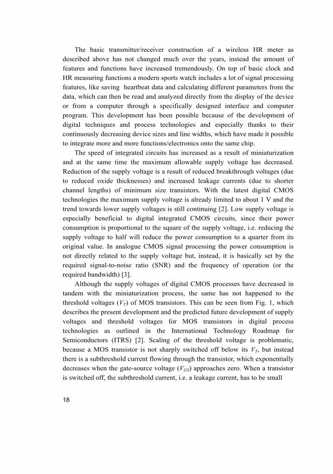
threshold voltages (VT) of MOS transistors. This can be seen from Fig. 1, which
describes the present development and the predicted future development of supply
voltages and threshold voltages for MOS transistors in digital process
technologies as outlined in the International Technology Roadmap for
Semiconductors (ITRS) [2]. Scaling of the threshold voltage is problematic,
because a MOS transistor is not sharply switched off below its VT, but instead
there is a subthreshold current flowing through the transistor, which exponentially
decreases when the gate-source voltage (VGS) approaches zero. When a transistor
is switched off, the subthreshold current, i.e. a leakage current, has to be small
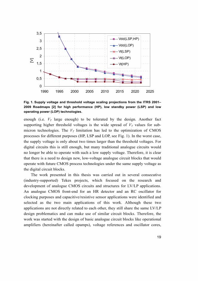
19
Fig. 1. Supply voltage and threshold voltage scaling projections from the ITRS 2001–
2009 Roadmaps [2] for high performance (HP), low standby power (LSP) and low
operating power (LOP) technologies.
enough (i.e. VT large enough) to be tolerated by the design. Another fact
supporting higher threshold voltages is the wide spread of VT values for sub-
micron technologies. The VT limitation has led to the optimization of CMOS
processes for different purposes (HP, LSP and LOP, see Fig. 1). In the worst case,
the supply voltage is only about two times larger than the threshold voltages. For
digital circuits this is still enough, but many traditional analogue circuits would
no longer be able to operate with such a low supply voltage. Therefore, it is clear
that there is a need to design new, low-voltage analogue circuit blocks that would
operate with future CMOS process technologies under the same supply voltage as
the digital circuit blocks.
The work presented in this thesis was carried out in several consecutive
(industry-supported) Tekes projects, which focused on the research and
development of analogue CMOS circuits and structures for LV/LP applications.
An analogue CMOS front-end for an HR detector and an RC oscillator for
clocking purposes and capacitive/resistive sensor applications were identified and
selected as the two main applications of this work. Although these two
applications are not directly related to each other, they still share the same LV/LP
design problematics and can make use of similar circuit blocks. Therefore, the
work was started with the design of basic analogue circuit blocks like operational
amplifiers (hereinafter called opamps), voltage references and oscillator cores,
0
0,5
1
1,5
2
2,5
3
3,5
1990 1995 2000 2005 2010 2015 2020 2025
[V]
Vdd(LSP,HP)
Vdd(LOP)
Vt(LSP)
Vt(LOP)
Vt(HP)
20
which were to be used as building blocks in the higher level designs. A primary
goal was to achieve LV operation compatible with the supply voltage limitations
of future CMOS process technologies. Another goal was to minimize power
consumption of the developed circuit blocks in order to achieve long battery-life
in portable applications. As a final outcome, the two main applications, i.e. an
analogue CMOS front-end for an HR detector and an RC oscillator for clocking
purposes and capacitive/resistive sensor applications, were designed,
manufactured and tested.
1.2 Structure of the thesis
The thesis is organized as follows: the electrical characteristics of an
electrocardiogram (ECG) signal is described in Chapter 2, the latter part of which
is devoted to reviewing different ECG measurement methods and circuit
implementations, as well as introducing the general structure of a preprocessing
stage for a QRS detector. The first part of Chapter 3 presents different types of
RC oscillators and discusses their suitability for clocking and resistive/capacitive
sensor interfaces, while the latter part concentrates on their circuit
implementations. Chapter 4 highlights the circuit level LV/LP design problems
related to the designed analogue integrated circuits and presents methods for
solving them. An overview of the published papers is given in Chapter 5. Two
LV/LP circuit level implementations and their performances are discussed in
Chapter 6, the first part of which is devoted to an analogue preprocessing stage
for a heart rate detector and the second part to an RC oscillator for clock and
sensor applications. A conclusion of the presented work is given in Chapter 7.
21
2 Heart rate measurements
The operation of the heart is based on electrical waves which cause the heart
muscle to pump blood. These electrical waves, which also pass through the body,
can be measured with electrodes attached to the skin. The electrodes are made of
conductive material, like metal or graphite, and the skin-electrode contact is often
ensured using electrolytic paste. Contractions of the heart, i.e. heartbeats, are seen
as spikes in the measured electrical waveform, which is called an
electrocardiogram (ECG). Depending on the positioning of the electrodes,
different projections of the ECG can be measured. Heart rate (HR) is an average
number of heartbeats per minute and can be calculated from the spikes of the
ECG.
HR can also be measured from the radial artery pressure (blood pressure)
pulse using electroacoustical or optical sensors. An electroacoustical sensor can
be realized with a piezo-microphone [4], which converts the blood pressure pulses
into electric pulses. An optical sensor can be implemented with a light source and
a receiver for measuring the amount of transmitted or reflected light, which is
modulated by the blood pressure pulses. The modulated light signal is then
converted into an electrical signal. This method is also called a
photopletysmography (PPG) [5-9]. Because the blood pressure pulse measured
with electroacoustical or optical sensors is in the same frequency and amplitude
range as the added noise caused by motion artifacts [8, 10], the signal-to-noise
ratio (SNR) of these methods cannot be improved by using conventional
frequency selective filters. Moreover, the power consumption of optical methods
is much higher than that of electroacoustical or electrical methods. This is due to
the need for a light source, usually a light emitting diode (LED) with typical
current consumption of a few milliamperes in continuous-time (CT) mode or a
little bit less in pulsed mode. Therefore, the main stream portable/wearable HR
meters have been realized with devices based on ECG.
2.1 Characteristic of the ECG signal
A typical healthy person’s ECG, measured with two electrodes on both sides of
the chest [11], is shown in Fig. 2. The amplitude and the shape of the waveform
will vary depending on the positioning of the sensor electrodes, but there are
certain parts of the waveform which can be recognized from all normal ECGs.
These parts are named in alphabetical order as P, Q, R, S and T waves. Fig. 3 –
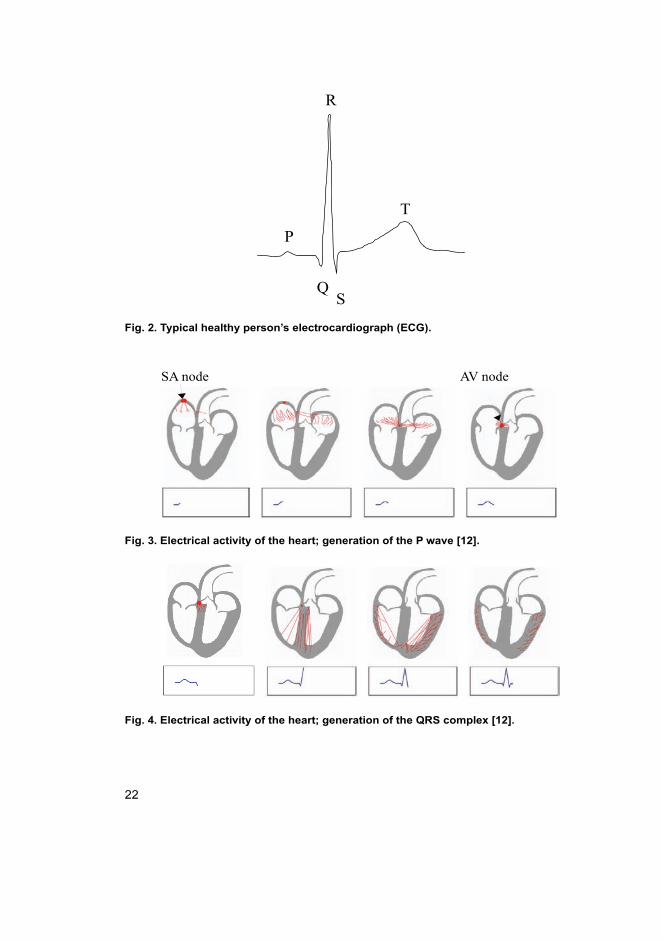
22
Fig. 2. Typical healthy person’s electrocardiograph (ECG).
Fig. 3. Electrical activity of the heart; generation of the P wave [12].
Fig. 4. Electrical activity of the heart; generation of the QRS complex [12].
AV node SA node
R
Q S
P
T

23
Fig. 5. Electrical activity of the heart; generation of the T wave [12].
Fig. 5 (reprinted from [12]) shows how these waves are generated. The P wave
represents atrial depolarization, where the electrical pulse starts from the
sinoatrial (SA) node and proceeds to the atrioventricular (AV) node and spreads
from the right atrium to the left atrium. The Q, R and S waves altogether form a
QRS complex which corresponds to the depolarization of the ventricles. Because
the ventricles have more muscle mass than the atriums, the QRS complex is larger
than the P wave. It is also sharper because of increased conduction velocity. The T
wave represents the repolarization of the ventricles.
With a ground-free measurement setup [11] with two electrodes on both sides
of the chest, the amplitude of the ECG can typically vary between 100 μV and 2
mV. The ECG signal also contains a DC offset voltage of up to 300 mV, which
develops across the skin-electrode interface due to an uneven distribution of
anions and cations. The cardiac signal is generally considered to contain
significant frequency components from 1 to 100 Hz, while the peak of the QRS
complex is normally found between 10 and 15 Hz [13]. The averaged power
spectra of a noiseless ECG, QRS complex and P- and T-waves (taken from [13])
are presented in Fig. 6.
Practical signal quality is also degraded by disturbances such as electrical
signals related to muscular activity (EMG), motion artifacts, variations in the
quality of the skin-electrode contacts, mains noise (50 or 60 Hz) and also inherent
signal variations, if these are large. The power spectra of muscle noise and motion
artifacts in comparison with the QRS complex and P- and T-waves (taken from
[13]) are presented in Fig. 7.
Since the QRS complex has the largest amplitude and the fastest rising and
falling times when compared to other parts of the ECG waveform (Fig. 2), it is
the easiest part to detect. As a contrast to clinical ECG measurements, in heart
rate (HR) measurements preserving the fine details of the ECG waveform is not

24
Fig. 6. Averaged power spectra of ECG, QRS complex and P- and T-waves [13] © 1994
IEEE.
Fig. 7. Averaged power spectra of QRS complex, P- and T-waves, muscle noise and
motion artefacts [13] © 1994 IEEE.
as important as reliable detection of the heartbeats, i.e. the QRS complexes.
Therefore, the other parts of the ECG signal (P- and T-waves), as well as other
disturbances, should be filtered out in order to enhance the detectability of the
QRS complexes.
25
2.2 QRS detection methods and implementations
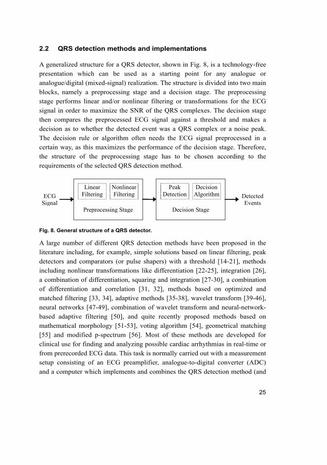
A generalized structure for a QRS detector, shown in Fig. 8, is a technology-free
presentation which can be used as a starting point for any analogue or
analogue/digital (mixed-signal) realization. The structure is divided into two main
blocks, namely a preprocessing stage and a decision stage. The preprocessing
stage performs linear and/or nonlinear filtering or transformations for the ECG
signal in order to maximize the SNR of the QRS complexes. The decision stage
then compares the preprocessed ECG signal against a threshold and makes a
decision as to whether the detected event was a QRS complex or a noise peak.
The decision rule or algorithm often needs the ECG signal preprocessed in a
certain way, as this maximizes the performance of the decision stage. Therefore,
the structure of the preprocessing stage has to be chosen according to the
requirements of the selected QRS detection method.
Fig. 8. General structure of a QRS detector.
A large number of different QRS detection methods have been proposed in the
literature including, for example, simple solutions based on linear filtering, peak
detectors and comparators (or pulse shapers) with a threshold [14-21], methods
including nonlinear transformations like differentiation [22-25], integration [26],
a combination of differentiation, squaring and integration [27-30], a combination
of differentiation and correlation [31, 32], methods based on optimized and
matched filtering [33, 34], adaptive methods [35-38], wavelet transform [39-46],
neural networks [47-49], combination of wavelet transform and neural-network-
based adaptive filtering [50], and quite recently proposed methods based on
mathematical morphology [51-53], voting algorithm [54], geometrical matching
[55] and modified p-spectrum [56]. Most of these methods are developed for
clinical use for finding and analyzing possible cardiac arrhythmias in real-time or
from prerecorded ECG data. This task is normally carried out with a measurement
setup consisting of an ECG preamplifier, analogue-to-digital converter (ADC)
and a computer which implements and combines the QRS detection method (and
Linear Filtering
Preprocessing Stage
NonlinearFiltering
Peak Detection
Decision Stage
Decision AlgorithmECG
Signal Detected Events
26
saving of the data) with a dedicated computer program. Therefore, these kinds of
detectors are also called as software QRS detectors [57]. An overview of and
comparison between several different detection methods is presented in [57] and
[58].
The detection methods implemented by the software QRS detectors are often
quite complex including features like calculation of the heart rate variability
(HRV) and automated classification of abnormal heartbeats from the ECG, which
makes them more suitable for stationary use in clinics for patient monitoring and
diagnostic purposes. For ambulatory use, such as for controlling the intensity of a
sporting exercise, the most important function is the real-time monitoring
capability of the user’s heart rate (HR). Therefore, the detector structure can be
simpler but it has to be optimized against motion artifacts, which are the most
dominant noise source while monitoring the HR of a moving target. Some of the
above-mentioned methods designed for portable use were implemented with
discrete components [24, 26, 29, 34] but, as expected, the lowest power
consumption and the smallest physical size is obtained with a fully integrated,
application specific integrated circuit (ASIC) [19-21, 25, 30, 33, 40, 42, 43, 45,
46]. Most of these integrated QRS detectors are based on linear filtering and peak
detection with a threshold. Some of them also include one or more nonlinear
transformations to enhance the QRS complexes. The rest of the reported solutions
are based on a wavelet transform.
There are very few fully integrated QRS detectors reported in the literature.
To the best of this author’s knowledge, the only ones also including sensor
interfaces are presented in [19-21]. The QRS detector chips presented in [19] and
[20] are intended to be used in the wireless, sensor/transmitter unit (a chest belt)
of a personal HR meter. These chips operate with supply voltages of 2.5 V – 3.3 V
and consume 30 μA (excluding the transmitter). The QRS detector chip developed
in [21] is a sensor node with a piezo-microphone sensor and a transmitter
interface, as suggested for a wireless health monitoring system. This chip operates
with a supply voltage of 0.9 V and consumes 7.5 μA in HR measurement mode.
Because the ECG signal obtained by a piezo-microphone HR sensor is much
higher than the signal obtained by electrodes (in the order of 100 mV(p-p) [59],
whereas it is typically 1-2 mV(p-p) [20]), the preamplifier can be simpler since it
does not necessarily need, for example, DC-offset compensation due to the low
need for amplification. On the other hand, the operation of a piezo-microphone
sensor is based on converting mechanical stress into electrical signals, which

27
makes it unsuitable for monitoring the HR during sporting activities because of
motion-related disturbances.
An integrated analogue signal processor (ASP) for HR extraction is proposed
in [25]. The ASP implements a robust peak detector based QRS detector, but it
needs an external preamplifier. The ASP is implemented with a 0.5 μm CMOS
process and consumes 4.5 mA from a supply of ±2 V.
The QRS detector presented in [30] is a digital system-on-chip (SoC)
realization which is implemented using standard cells from the manufacturer’s
design library. The core of the design is a hard macro cell of a 32-bit reduced
instruction set computer (RISC) with memory and bus controllers. The chip needs
an external preamplifier and an ADC. The chip is implemented with a 0.18 μm
1.8 V/3.3 V CMOS technology, but there is no information about the power
consumption.
A programmable DSP ASIC for HR measurements is presented in [33]. This
chip also needs an external preamplifier and an ADC. The chip is implemented
with a 1.0 μm CMOS technology, but neither the supply voltage nor the power
consumption has been reported.
An analogue QRS detector chip based on wavelet transform (WT) is
presented in [40]. This chip implements a WT, an absolute value circuit, a peak
detector and a comparator by means of dynamic translinear (DTL) circuit
technique [60]. The WT system has 5 parallel scales and its power consumption is
55 nW per scale from a 2-V supply. This chip is implemented with a semi-custom
bipolar IC process.
The rest of the published QRS detectors [42, 43, 45, 46] are based on digital
WT and they also need external preamplifiers and ADCs. The design presented in
[43], which is a developed version of [42], is implemented with 0.13 μm CMOS
technology with supply voltage of 1.2 V. It includes a wavelet filter bank and a
generalized likelihood ratio test with a threshold function. Estimated power
consumption based on simulations in alert and normal mode is 114 nW and 37.9
nW, respectively. The QRS detector chip presented in [45] contains a wavelet
filter bank and a multi-scale multiplier with a threshold function and it is
implemented with 0.18 μm CMOS technology. Simulated power consumption is
644.9 nW, when all wavelet filters are active and 318.4 nW in normal operation,
when half of the filters are switched off. It is worth mentioning here that over
90% of the power consumption of this chip is caused by leakage currents, which
are a serious problem with deep sub-micron technologies. The ECG signal
processor proposed in [46] includes a wavelet filter bank and denoising block
28
followed by heartbeat rate prediction and classification blocks. This chip is an
SRAM-based ASIC architecture, which is realized with 0.18 μm CMOS
technology. The chip consumes 29 μW from a 1-V supply.
All of the above-mentioned QRS detectors are aimed at non-invasive
measurement of the HR, but modern implantable pacemakers, like the one
presented in [61], also include an HR measurement function. In pacemaker
applications the supply voltage is usually higher, in the order of 2.8 V, because of
the need to generate high-voltage (~ 5 V) pulses to stimulate the heart muscle (for
example, to initiate a heart-beat). The high-voltage pulse is generated with a
capacitive voltage multiplier. Because the pacemaker is implanted inside the body
of the user, the pacemaker chip has to be optimized for very low-power
consumption in order to achieve a long battery-life. Therefore, the chip proposed
in [61] is implemented with a special 0.5 μm multi-VT process, consuming only 8
μA from a 2.8-V supply. Although the structure of the QRS detector is not
presented it is presumably not compatible with very low supply voltages.
As a final note, it can be concluded that several integrated low-power (LP)
analogue/digital QRS detectors have been reported in the literature, but only a
few of them are capable of very low supply voltage operation of 1 V or less.
Moreover, none of them contains a preamplifier with adequate performance for
ECG measurements operating with 1 V or less. Since the preprocessing stage of
the QRS detector always needs an analogue interface between the ECG sensors
and the analogue or digital signal processor, it is also important to find a way to
implement that in a low-voltage (LV) environment. Therefore, this work has been
focused on developing analogue LV/LP circuit blocks and a sensor interface for
the preprocessing stage of a QRS detector.
2.3 Preprocessing stage for a QRS detector
As described in Chapter 2.2 a preprocessing stage performs linear and/or
nonlinear filtering/transformations for the ECG signal in order to maximize the
SNR of the QRS complexes (Fig. 8). A practical realization also includes an ECG
amplifier in front of the preprocessing stage. The amplifier is needed to increase a
weak ECG signal, which may vary from 100 μV to 2 mV measured with
electrodes, at a reasonable level for further processing. The next stage is either an
analogue signal processing (ASP) block or an analogue-to-digital converter (ADC)
followed by a digital signal processing (DSP) block. It is also possible to do one
part of the signal processing in analogue domain and the other part in digital
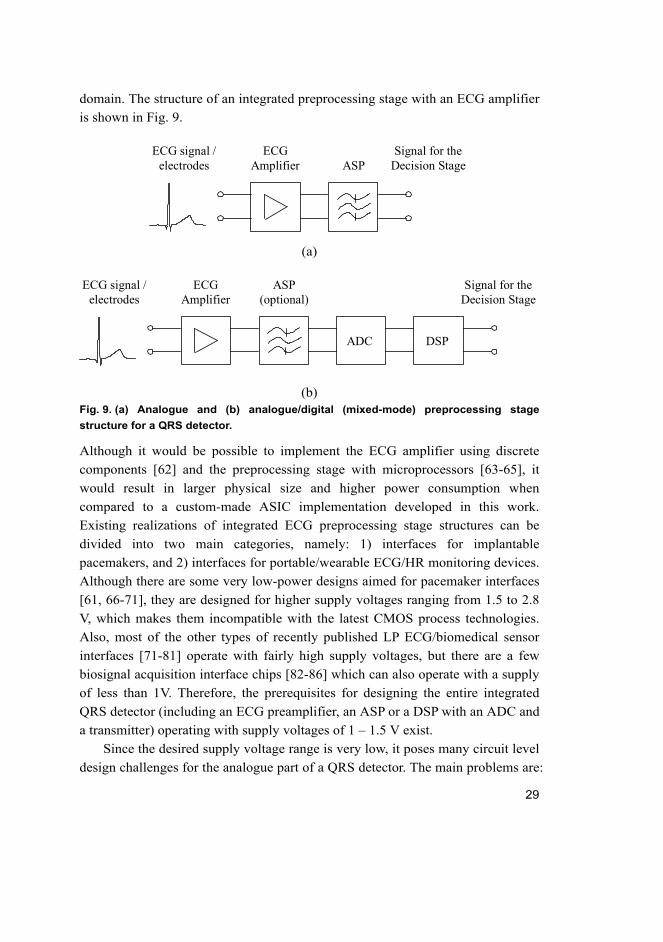
29
domain. The structure of an integrated preprocessing stage with an ECG amplifier
is shown in Fig. 9.
ECG
Amplifier ASP Signal for the
Decision StageECG signal /
electrodes
(a)
ECG
Amplifier ASP
(optional)Signal for the
Decision Stage ECG signal /
electrodes
ADC
DSP
(b)
Fig. 9. (a) Analogue and (b) analogue/digital (mixed-mode) preprocessing stage
structure for a QRS detector.
Although it would be possible to implement the ECG amplifier using discrete
components [62] and the preprocessing stage with microprocessors [63-65], it
would result in larger physical size and higher power consumption when
compared to a custom-made ASIC implementation developed in this work.
Existing realizations of integrated ECG preprocessing stage structures can be
divided into two main categories, namely: 1) interfaces for implantable
pacemakers, and 2) interfaces for portable/wearable ECG/HR monitoring devices.
Although there are some very low-power designs aimed for pacemaker interfaces
[61, 66-71], they are designed for higher supply voltages ranging from 1.5 to 2.8
V, which makes them incompatible with the latest CMOS process technologies.
Also, most of the other types of recently published LP ECG/biomedical sensor
interfaces [71-81] operate with fairly high supply voltages, but there are a few
biosignal acquisition interface chips [82-86] which can also operate with a supply
of less than 1V. Therefore, the prerequisites for designing the entire integrated
QRS detector (including an ECG preamplifier, an ASP or a DSP with an ADC and
a transmitter) operating with supply voltages of 1 – 1.5 V exist.
Since the desired supply voltage range is very low, it poses many circuit level
design challenges for the analogue part of a QRS detector. The main problems are:
30
1) a limited dynamic range (DR) and consequently 2) a reduced signal-to-noise
ratio (SNR) of the analogue interface connected to the ECG sensors and 3) an
insufficient drive voltage to operate all switches of conventional switched
capacitor (SC) circuits. These problems are discussed in more detail in Chapter 4.
The problems related to the limited DR and SNR of the QRS detector are
reduced to the signal swing limitations of the used opamps, and more specifically
to their input stages, which are discussed in Chapters 4.1.1 – 4.1.3. In order to
achieve an adequate DR for the QRS detector, two opamps with different types of
input stages, i.e. floating-gate (FG) and bulk-driven (BD) input stages, have been
designed and published in Papers I and II to study their possible advantages over
the opamps equipped with conventional input stages.
The problems and solutions concerning analogue switches in SC circuits are
introduced in Chapter 4.2 and the concept of a switched-opamp is presented in
Chapter 4.3. The idea behind the switched-opamp circuit is to achieve a lower
minimum supply voltage for an SC circuit by removing the need for critical series
switches from the signal path. A critical switch is a switch which needs to conduct
the whole signal swing, for example, from the output of an opamp to a sampling
capacitor. The minimum possible supply voltage for an SC circuit can be
achieved if all switches can be switched either against the positive or the negative
(usually ground) supply voltage. As a result of these studies, a whole LV/LP QRS
detector interface, including a sensor interface and a switched-opamp switched-
capacitor (SO-SC) filter, is presented in Papers VI and VII, while the design
choices, performance and future work of this design are also discussed in Chapter
6.1.
31
3 RC oscillators
A low-voltage low-power (LV/LP) RC oscillator was chosen as another important
application to be developed in this work. The aim was to design an initially
accurate RC oscillator (which does not need any calibration or additional
reference) that could be used both as a capacitive/resistive sensor interface in
sensor applications or as a clock circuit in discrete-time (DT) analogue/mixed-
signal designs. An RC oscillator could also be used in communication links such
as Universal Asynchronous Receiver Transmitter (UART) circuits if frequency
variation is kept within ±1%. Therefore an accuracy of ±1% is considered
adequate for the foreseen clocking purposes and the tuning/sensing range of ±1
decade enough for external circuit elements/sensors R and C. The target supply
voltage for the RC oscillator is 1 – 1.5 V, and the power consumption is in a range
of microwatts.
Traditionally RC oscillators have been used in applications like tone
generators, alarms and flashing lights where only moderate accuracy is required.
This is due to the fact that an accurate operating frequency and a small
temperature drift are much easier to realize with a crystal oscillator.
Commercially available quartz crystals and crystal oscillators can easily achieve
an initial accuracy of 10 ppm with a temperature drift of less than 0.05 ppm/°C.
Therefore, they are the most frequently used solution for time keeping and
clocking purposes. The benefits of an RC oscillator over a crystal oscillator are
the possibility of adjusting the frequency and integrating all components onto one
chip. Passive components R and C are also much cheaper than quartz crystals,
which might be a selection criterion especially in large production series. In order
to achieve a good accuracy with an RC oscillator, circuit elements R and C must
be either external precision components or trimmable integrated components. In
both cases the expected frequency accuracy and temperature drift, which are
typically within few percent, are quite modest when compared with the
performance of a crystal oscillator. However, an RC oscillator can be used as a
clock generator in many applications such as microprocessors, hearing-aid
devices, pacemakers, sensor ICs and other SoCs where extreme accuracy is not
required.
Recently, interest has grown in RC oscillators, especially in sensor
applications where either R or C is replaced with a resistive or a capacitive sensor.
With these sensors it is possible to measure, for example, pressure, temperature
and humidity [87, 88]. The idea is to convert changes in resistance or capacitance
32
to changes of frequency, which is actually one kind of an analogue-to-digital
(A/D) conversion. Depending on the application, the output can be used, for
example, to adjust a process variable, as an alarm when preset threshold levels are
exceeded or by displaying a parameter value under measurement.
There are several ways to realize an RC oscillator depending on the
requirements of the application. Referring to their output, classical RC oscillators
can be divided into two main categories: linear (sine-wave) and nonlinear
(square-wave, triangular or sawtooth) oscillators. The most common topologies of
both categories are presented in the following subchapters.
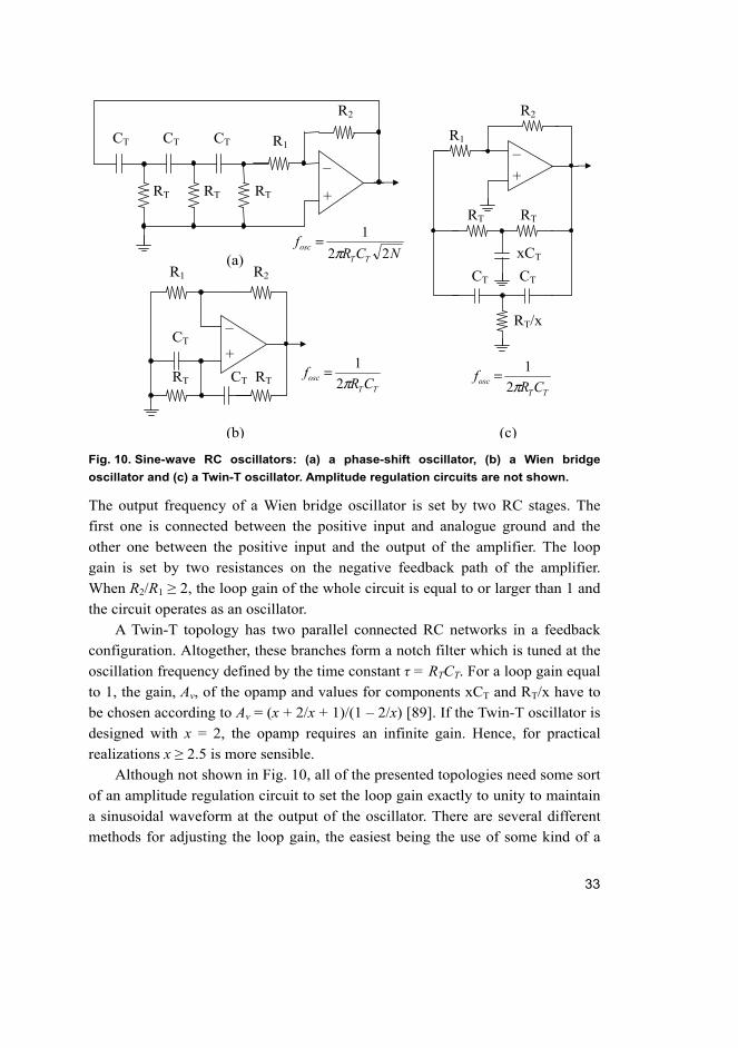
3.1 Linear RC oscillators
A linear (sine-wave) RC oscillator consists of two parts made up of a tuned RC
network and an amplifier in a feedback configuration. The amplifier can be either
an opamp or a simpler amplifier stage with one or a few more transistors. The
most common linear RC oscillators, namely a phase-shift oscillator, a Wien
bridge oscillator and a Twin-T oscillator, are presented in Fig. 10.
In order to operate as an oscillator, all these circuits need to meet
Barkhausen’s criterion, which states that the loop gain at the oscillation frequency
is equal to unity and the total phase shift around the loop is zero or a multiple
integer of 2π (360°), i.e. n·2π (n·360°), where n = 0,1,2,… The operation principle
of each oscillator topology is briefly explained in the following paragraphs and a
more detailed analysis of these circuits can be found, for example, from [89].
In case of a phase-shift oscillator, the frequency of oscillation, fosc, is defined
by the time constant τ = RTCT and the number (N) of consecutive RC stages in a
feedback loop. The oscillator settles to a frequency where the total phase shift of
the loop is 0°. One part of the total phase shift is due to the inverting amplifier
(-180°) and the other part due to the RC chain (+180°) in a feedback loop. The
minimum amount of RC stages capable of producing a 180° phase shift at a finite
frequency is three. Therefore, the phase shift in case of three consecutive RC
stages is 60° per stage. For a loop gain of 1, the opamp’s gain has to be |Av| =
R2/R1 ≥ 29 and R1 must be sufficiently large, for instance R1 > 10RT, to minimize
the loading of the opamp.
33
Fig. 10. Sine-wave RC oscillators: (a) a phase-shift oscillator, (b) a Wien bridge
oscillator and (c) a Twin-T oscillator. Amplitude regulation circuits are not shown.
The output frequency of a Wien bridge oscillator is set by two RC stages. The
first one is connected between the positive input and analogue ground and the
other one between the positive input and the output of the amplifier. The loop
gain is set by two resistances on the negative feedback path of the amplifier.
When R2/R1 ≥ 2, the loop gain of the whole circuit is equal to or larger than 1 and
the circuit operates as an oscillator.
A Twin-T topology has two parallel connected RC networks in a feedback
configuration. Altogether, these branches form a notch filter which is tuned at the
oscillation frequency defined by the time constant τ = RTCT. For a loop gain equal
to 1, the gain, Av, of the opamp and values for components xCT and RT/x have to
be chosen according to Av = (x + 2/x + 1)/(1 – 2/x) [89]. If the Twin-T oscillator is
designed with x = 2, the opamp requires an infinite gain. Hence, for practical
realizations x ≥ 2.5 is more sensible.
Although not shown in Fig. 10, all of the presented topologies need some sort
of an amplitude regulation circuit to set the loop gain exactly to unity to maintain
a sinusoidal waveform at the output of the oscillator. There are several different
methods for adjusting the loop gain, the easiest being the use of some kind of a
R1 R2
RT RT CT
CT _
+
TTosc CR
fπ2
1=
(c)
(a)
CT CT CT
RT RT RT
NCRf
TT
osc22
1
π=
_
+
R2
R1 _
+
RT
RT/x
CT
xCT
TTosc CR
fπ2
1=
R2
R1
RT
CT
(b)
34
nonlinear element in the feedback loop, which causes the loop gain with small
amplitude levels to be larger than unity and with too large amplitude levels less
than unity. The simplest possible realization of this type of nonlinearity is an
amplifier with an amplitude regulated output, although for low distortion and
precisely controlled amplitude, a more sophisticated nonlinearity is required.
Because the output frequency of all topologies presented in Fig. 10 is
determined by multiple resistors and capacitors with certain component ratios,
they are more suitable for clocking than sensor applications.
3.2 Nonlinear RC oscillators
Nonlinear (square-wave, triangular or sawtooth) RC oscillators are often called
relaxation oscillators. The term “relaxation” refers to charging and discharging
phases of a capacitor. There are many types of relaxation oscillators, starting from
simple two-transistor multivibrator circuits to more complex topologies, but they
all share the same operation principle. Fig. 11 presents two examples of a
relaxation oscillator, which are astable multivibrator circuits based on a single
comparator and a commonly used relaxation oscillator topology which allows the
adjustment of its parameters more freely.
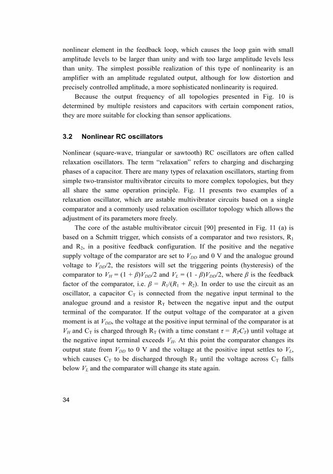
The core of the astable multivibrator circuit [90] presented in Fig. 11 (a) is
based on a Schmitt trigger, which consists of a comparator and two resistors, R1
and R2, in a positive feedback configuration. If the positive and the negative
supply voltage of the comparator are set to VDD and 0 V and the analogue ground
voltage to VDD/2, the resistors will set the triggering points (hysteresis) of the
comparator to VH = (1 + β)VDD/2 and VL = (1 - β)VDD/2, where β is the feedback
factor of the comparator, i.e. β = R1/(R1 + R2). In order to use the circuit as an
oscillator, a capacitor CT is connected from the negative input terminal to the
analogue ground and a resistor RT between the negative input and the output
terminal of the comparator. If the output voltage of the comparator at a given
moment is at VDD, the voltage at the positive input terminal of the comparator is at
VH and CT is charged through RT (with a time constant τ = RTCT) until voltage at
the negative input terminal exceeds VH. At this point the comparator changes its
output state from VDD to 0 V and the voltage at the positive input settles to VL,
which causes CT to be discharged through RT until the voltage across CT falls
below VL and the comparator will change its state again.
35
Fig. 11. Nonlinear (square-wave) RC oscillators: (a) an astable multivibrator based on
a Schmitt trigger and (b) a relaxation oscillator.
The output frequency fosc of the oscillator presented in Fig. 11 (a) is ideally a
function of the feedback factor β and the time constant τ = RTCT. In practice, fosc
is also dependent on VDD variations and the comparator’s state-to-state transition
delays (tD(tot)), which together add up to the oscillation period. Variations in VDD
will also affect the threshold voltages VH and VL and the charging/discharging
current of CT. Therefore, the described simple multivibrator circuit is more
suitable for low frequency applications with low accuracy requirements, such as
flashing lights and tone alarms.
Another relaxation oscillator, presented in Fig. 11 (b), is a commonly used
topology which consists of a digital SR latch driven by two comparators with
presettable threshold voltages, a timing capacitor and a constant current
sink/source. In this case, the timing capacitor is charged and discharged with a
constant current IC, which can be set, for example, by a resistor in a bias circuit.
The voltage VC across the capacitor is compared against two threshold voltages
)(1
1ln2
1
totDTT
osc
tCR
f
+
−+
=
ββ
R1 R2
CT RT
_ +
Vout
21
1
RR
R
+=β
Tosc = T + tD(tot)
VL
VH
VDD
VCT
Vout
(a)
VC
S
VL R
IC
Q
C _
+
_
+
IC
VH
VDD
Vout
(b)
Tosc = T + tD(tot)
VDD
VL
VH VC
Vout
( )
12 ( )osc
H LD tot
C
fC V V
tI
= − +
36
VH and VL with two comparators. Whenever the capacitor voltage reaches either
of the thresholds, the SR latch toggles and reverses the direction of the capacitor
current. Ideally, the oscillation frequency would be directly proportional to the
capacitor current and inversely proportional to the capacitor value and the
difference of the threshold voltages, but again the delays (tD(tot)) introduced by the
comparators and the latch of the level detection circuit (causing overshooting of
the threshold voltages) add up to the output period, which causes the actual
oscillation frequency to be lower than ideal. This effect increases towards higher
frequencies.
Since it is possible to set the output frequency of a relaxation oscillator with
only one resistor and capacitor (or corresponding sensor element), it is a better
choice for sensor applications than the linear topologies presented in Chapter 3.1.
Relaxation oscillators can also be used as clock generators, which allow the clock
frequency to be tuned with minimum amount of passive components. However,
the delays introduced by the comparators add up to the period which limits the
frequency accuracy of this type of oscillator at high frequencies.
The next chapter summarizes the state-of-the-art LP RC oscillators suitable
for both sensor and clock applications. All presented topologies are based on the
relaxation oscillator principle.
3.3 RC oscillator implementations
Since the introduction of the 555 timer, RC oscillators have been used in
commercial applications as clock, pulse, delay and ramp generators. The 555
timer is based on a relaxation oscillator topology, presented in Fig. 11 (b), and is
available both as bipolar and CMOS versions. Although the latest CMOS versions
are able to operate with supply voltages as low as 1.5 V (LMC555) or even 1 V
(TLC551, which has the same pinout and functionality as the 555 type of timer),
their maximum operating frequency is only up to a few MHz because of the
delays present in the comparators and the parasitic capacitances and resistances
related to the I/O timing pins. Furthermore the current consumption of general
purpose RC timers is typically quite high, up to 1 – 10 mA, which is too high for
LP applications. There are also some LP timers, such as LTC6906, which
consumes only 12 μA at 100 kHz operating frequency, but its minimum supply
voltage is 2.25 V and it can operate only up to 1 MHz frequency.
On the other hand, the overall frequency accuracy of the above-mentioned
RC oscillators depends not only on the values of passive circuit elements R and C

37
but also on the comparator’s “high-to-low” and “low-to-high” transition delays,
both of which are functions of supply voltage and temperature. These delays will
decrease the frequency stability at high frequency in clock applications and the
measurement linearity in resistive or capacitive sensor applications. Therefore,
the circuit topologies presented in these commercially available ICs do not satisfy
the requirements set for this work.
If an RC oscillator is used only for clocking purposes, circuit elements R and
C can be realized with either external or integrated components. In case of a fully
integrated RC oscillator, the value of the RC time constant without tuning can
vary up to ±40%. In addition, the temperature coefficient (TC) of integrated
resistors is quite large, in the order of 1000 – 3000 ppm/°C [91], which also has to
be taken into account when designing an accurate clock generator. On the other
hand, the TC of integrated capacitors is negligible. Therefore, an accurate
integrated RC oscillator should not only provide some kind of temperature
compensation scheme for the resistor but also the opportunity to tune the
operating frequency of the whole RC oscillator. Another way is to use an accurate
and temperature compensated external time constant RC instead of integrated R
and C.
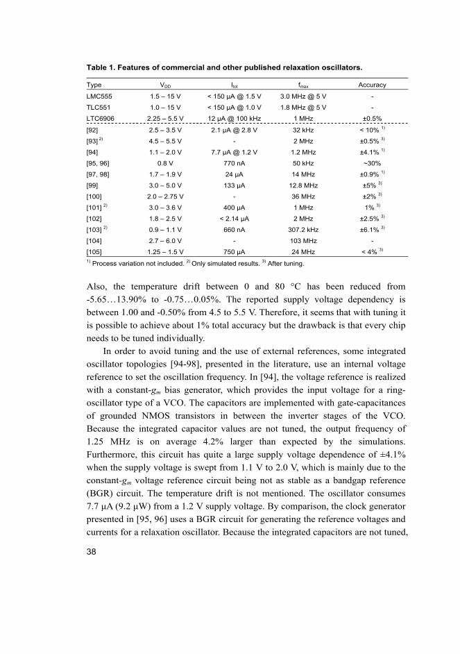
Table 1 summarizes the performance of commercial and other published
relaxation oscillators with respect to the most important parameters for an RC
oscillator set in this current work. Commercial timer circuits are listed above and
other published relaxation oscillators below the dashed line.
The design presented in [92] is a relaxation type 32-kHz RC oscillator with
internal C and external R without tuning. The initial frequency accuracy of the
oscillator (which is not reported) mainly depends on the process variation of the
integrated C and the delay of the comparator. The comparator alone causes an
estimated additional delay of 13% for the oscillation period at 32-kHz operating
frequency. The measured standard deviation for the chip-to-chip variation is about
4.3%, the supply voltage dependence -2.3%/V from 2.5 to 5 V and the
temperature drift -3% from -20 to 70 °C.
Reference [93] presents a fully integrated RC oscillator, which includes a
digitally trimmed resistor to eliminate the process variations and a simple
temperature drift compensation circuit realized with a combination of an
integrated resistor with a negative TC and a transistor with a positive TC.
Simulation results show that the output frequency span with worst case simulation
corner parameters with and without trimming is ±0.5% and ±40%, respectively.
38
Table 1. Features of commercial and other published relaxation oscillators.
Type VDD Itot fmax Accuracy
LMC555 1.5 – 15 V < 150 μA @ 1.5 V 3.0 MHz @ 5 V -
TLC551 1.0 – 15 V < 150 μA @ 1.0 V 1.8 MHz @ 5 V -
LTC6906 2.25 – 5.5 V 12 μA @ 100 kHz 1 MHz ±0.5%
[92] 2.5 – 3.5 V 2.1 μA @ 2.8 V 32 kHz < 10% 1)
[93] 2) 4.5 – 5.5 V - 2 MHz ±0.5% 3)
[94] 1.1 – 2.0 V 7.7 μA @ 1.2 V 1.2 MHz ±4.1% 1)
[95, 96] 0.8 V 770 nA 50 kHz ~30%
[97, 98] 1.7 – 1.9 V 24 μA 14 MHz ±0.9% 1)
[99] 3.0 – 5.0 V 133 μA 12.8 MHz ±5% 3)
[100] 2.0 – 2.75 V - 36 MHz ±2% 3)
[101] 2) 3.0 – 3.6 V 400 μA 1 MHz 1% 3)
[102] 1.8 – 2.5 V < 2.14 μA 2 MHz ±2.5% 3)
[103] 2) 0.9 – 1.1 V 660 nA 307.2 kHz ±6.1% 3)
[104] 2.7 – 6.0 V - 103 MHz -
[105] 1.25 – 1.5 V 750 μA 24 MHz < 4% 3) 1) Process variation not included. 2) Only simulated results. 3) After tuning.
Also, the temperature drift between 0 and 80 °C has been reduced from
-5.65…13.90% to -0.75…0.05%. The reported supply voltage dependency is
between 1.00 and -0.50% from 4.5 to 5.5 V. Therefore, it seems that with tuning it
is possible to achieve about 1% total accuracy but the drawback is that every chip
needs to be tuned individually.
In order to avoid tuning and the use of external references, some integrated
oscillator topologies [94-98], presented in the literature, use an internal voltage
reference to set the oscillation frequency. In [94], the voltage reference is realized
with a constant-gm bias generator, which provides the input voltage for a ring-
oscillator type of a VCO. The capacitors are implemented with gate-capacitances
of grounded NMOS transistors in between the inverter stages of the VCO.
Because the integrated capacitor values are not tuned, the output frequency of
1.25 MHz is on average 4.2% larger than expected by the simulations.
Furthermore, this circuit has quite a large supply voltage dependence of ±4.1%
when the supply voltage is swept from 1.1 V to 2.0 V, which is mainly due to the
constant-gm voltage reference circuit being not as stable as a bandgap reference
(BGR) circuit. The temperature drift is not mentioned. The oscillator consumes
7.7 μA (9.2 μW) from a 1.2 V supply voltage. By comparison, the clock generator
presented in [95, 96] uses a BGR circuit for generating the reference voltages and
currents for a relaxation oscillator. Because the integrated capacitors are not tuned,

39
the simulated 1σ and 3σ variations of the output frequency are 4% and 11.85%,
respectively, the TC 842 ppm/°C from 0 to 80 °C and the supply voltage variation
-2.5%/V from 1 to 1.5 V. The measured chip-to-chip variation with a 0.8 V supply
voltage is large, close to 30%, and the operating frequency starts to decrease
rapidly above 0.8 V, which behavior the authors could neither explain nor
reproduce by simulations. The measured TC from 20 to 60 °C is 0.3%/°C.
A relaxation oscillator presented in [97, 98] is a fully integrated RC oscillator,
which uses a voltage averaging feedback circuit with a voltage reference
proportional to supply voltage. This circuit is shown to be quite insensitive to
supply voltage variations because of the operation principle. On the other hand,
the temperature dependency relies on the TC of the integrated R and the total
accuracy on both R and C in the oscillator core. The oscillator achieves a
measured TC of ±0.75% from -40 to 125 °C and a supply voltage variation of
±0.16% from 1.7 to 1.9 V. Neither the chip-to-chip variation nor the absolute
accuracy of the output frequency is published.
In references [99-101], the use of an internal voltage reference has been
combined with trimming of the output frequency. In [99], a BGR is used for
generating temperature compensated reference voltages for the comparators and
currents for charging/discharging the capacitors in a relaxation oscillator. The
timing capacitor is comprised of an 8-bit binary-weighted capacitor array to
cancel out the effects of process variations. This oscillator achieves ±5% total
frequency accuracy including process variations, supply voltage variation from 3
to 5 V and temperature range of -40 to 125 °C without any external components.
The same idea has been utilized in [100], which presents a relaxation oscillator
with a BGR and a 5-bit capacitor array. This oscillator operates with a supply
voltage down to 2 V and it achieves ±5% frequency accuracy with a supply
voltage range of 2.5 V ±10% and a temperature range from 0 to 80 °C without
external components.
The RC oscillator proposed in [101] uses an external resistor, an integrated
capacitor and a reference voltage based on a resistor ratio with a tuning circuit.
The use of an external resistor ensures a low temperature variation (if a low-TC
component is used) and the tunable reference voltage can be used to cancel out
the process variations. This oscillator achieves a total simulated frequency
accuracy of 1% with supply voltage variation of 3.3 V ±10% and a temperature
range from -40 to 125 °C.
Two LP RC oscillators for capacitive sensor applications are presented in
[102, 103]. The oscillator, described in [102], consists of a source-coupled CMOS
40
multivibrator, a proportional-to-absolute-temperature (PTAT) bias circuit and a
two-stage comparator. The bias circuit is provided with a programmable resistor
matrix and the oscillator with a capacitance matrix to enable calibration. After
calibration the oscillator achieves an operating frequency of 2 MHz with a total
accuracy of ±2.5% including a supply voltage variation of ±10% and a
temperature range from -35 °C to +85 °C. The typical power consumption with a
1.8-V supply voltage at room temperature is 3.0 μW. The circuit operates with
supply voltages from 1.8 to 2.5 V. The oscillator presented in [103] is a modified
version of [102] and it consists of two parallel tunable oscillators (only one
operates at a time) with different operating frequencies to cover a larger range of
operating frequencies. Because of a lower supply voltage of 1 V used by this
design, the floating capacitance matrix of [102] has been replaced with a fixed
capacitor and tuning is accomplished with a resistor matrix. The simulation
results for this double-mode oscillator in modes 1 and 2 show a frequency
stability of 24.6 kHz ±10.7% and 307.2 kHz ±6.1% with a supply voltage
variation of 1 V ±10% and a temperature range from -40 to 85 °C. The current
consumption in modes 1 and 2 are 210 nA and 660 nA, respectively.
Reference [104] presents an RC oscillator topology which places a ring-
oscillator type of VCO in a feedback loop of a relaxation type RC oscillator. This
oscillator samples its own period and compares it to the RC time constant. One
advantage of this operation principle is that it uses a frequency divider to separate
the operating frequency of the VCO from the charging/discharging frequency of
the capacitor. As a result, the output frequency of the oscillator and the values for
passive components can be selected more freely. Another advantage is that the
negative feedback loop corrects all variations caused by temperature, supply
voltage and process variations. The total accuracy of the oscillator, presented in
[104], depends only on the RC time constant itself, added with the accuracy of the
frequency divider and a current mirror ratio. Because the division ratio can be
assumed ideal, the final accuracy reduces to the accuracies of the RC time
constant and the current mirror ratio. The reported performance (excluding
variations of external components R and C) shows that the maximum operating
frequency is 103 MHz, the supply voltage sensitivity 3,430 ppm/V or 1.13% from
2.7 V to 6.0 V and the temperature sensitivity 57.1 ppm/°C (the temperature range
is not reported).
The RC oscillator, presented in [105], uses the operation principle described
in [104] with an added tuning option. After tuning the oscillator achieves a total
frequency accuracy of 4%, including process variations, supply voltage variations
41
from 1.25 to 1.5 V, temperature variations from -40 to 85 °C and 1% component
variation in external RC time constant.
As a conclusion for this review, it may be noted that there are several RC
oscillator topologies which satisfy the requirements of LV/LP operation but most
of them do not reach the desired total frequency accuracy of < ±1% even if tuned,
which was one of the goals in this particular piece of work. Without tuning, none
of the LV/LP designs is even close to this target. The most promising topology of
the RC oscillators described above is the one presented in [104], which allows
choosing the component values and the frequency of operation more freely. This
is an important feature when aiming for low power consumption, high frequencies
or an optimized sensor interface with a certain impedance range. Therefore, the
idea presented in [104] has been adopted for the design of an accurate LV/LP RC
oscillator for clock and sensor applications, two versions of which are presented
in Papers IV and VIII. The design choices, performance and future work of this
design are presented in Chapter 6.2.

42
43
4 Problems and solutions for LV/LP issues in analogue circuit design
This chapter concentrates on practical circuit level design problems and their
viable solutions concerning two main applications, i.e. a low-voltage, low-power
(LV/LP) preprocessing stage for a heart rate detector and an LV/LP RC oscillator,
developed in this work. Since the desired supply voltage range set for this work is
very low, i.e. VDD(min) ≤ 2VT + Vov, it poses many design challenges for both
continuous-time (CT) and discrete-time (DT) analogue signal processing (ASP)
circuits.
One of the most important issues caused by low supply voltage is the limited
dynamic range (DR) of a circuit. The DR is the range between the maximum and
the minimum signal levels. The maximum is limited by the supply voltage and the
minimum by the noise floor. In order to achieve a reasonable DR and signal-to-
noise ratio (SNR) for an ASP, it is desirable to keep the signal amplitude as large
as possible throughout the whole circuit. Because amplifiers, filters and other
active ASP circuit blocks are most often realized with opamps, the DR limitations
of the analogue part is reduced to limitations of the opamps and, more specifically,
their input stages. With a conventional input stage consisting of a gate-driven
differential pair with a current sink (or source) this limitation manifests as an
input signal common-mode range (CMR) limited close to the other rail of the
supply voltages. An output stage for an opamp is easier to design for rail-to-rail
operation and therefore the output voltage swing can be maximized by centering
it in between the supply voltages. Depending on the application the input voltage
CMR limitation can be crucial.
In case of an ECG amplifier, presented in Fig. 9 as a part of a QRS detector,
the input signal level is very small, less than 2 mV. Therefore, the input CMR
does not need to be large. However, the problem is that the input CMR of a
conventional input stage with gate-driven differential pair does not reach the mid-
supply at low supply voltages. If the ECG amplifier is realized with a single-
ended (SE) opamp (differential input and SE output) with a resistive feedback
loop setting the gain, then the linear output swing and the DR of the amplifier will
be limited. This is due to the fact that the feedback path from the output to the
input of the amplifier sets the output DC operating point equal to the input DC
operating point, which is close to the other supply rail. Therefore, the linear
output voltage swing is also limited closer to the other supply rail. On the other
hand, if the ECG amplifier is realized with a fully-differential (FD) opamp, then
44
the problem is in the design of the common-mode feedback (CMFB) circuit.
Since traditional CMFB circuits have been designed using circuit structures
similar to the input stages of opamps, either the resulting output swing of the FD
opamp is very limited (equal to the CMR of the input stage) or the input stage of
the CMFB circuit needs to be redesigned for rail-to-rail operation.
In another application, i.e. an RC oscillator developed in this work, two
analogue voltages with a large dynamic range are compared with each other in
order to set the output frequency of the oscillator. In this case, the input stage
needs to have a rail-to-rail input voltage capability. A rail-to-rail input CMR can
be achieved, for example, with a floating-gate (FG) input stage or a bulk-driven
(BD) input stage, both of which are introduced in Chapters 4.1.2 and 4.1.3,
respectively.
Analogue low-voltage (LV) discrete-time (DT) circuit blocks, like switched-
capacitor (SC) filters, suffer not only from the input CMR problems but also from
switching problems. This is due to the reduced conductivity of a CMOS switch
during its “on” state when the supply voltage is equal to or less than the sum of
the threshold voltages of the switch transistors. This problem is mainly caused by
series CMOS switches on the signal path. These series switches are usually
located as the first switches in front of the SC circuit or at the outputs of the
opamps inside the SC circuit. When the output voltage of an opamp is closer to
the positive or the negative supply rail, either the PMOS or the NMOS transistor
of the CMOS switch conducts the signal. When the output voltage (i.e. the signal)
is around the mid-supply, neither the PMOS nor the NMOS transistor is able to
conduct, a factor which will destroy the operation of the whole circuit. The series
switch at the output of an opamp can be avoided by replacing both the switch and
the opamp with a so-called switched-opamp circuit, which either turns the output
stage or the whole opamp off during its non-active phase. Since the analogue
signal processing (ASP) block for a QRS detector, presented in Fig. 9 (Chapter
2.3), is implemented using SC techniques, switching problems and their solutions
will be discussed more specifically in Chapters 4.2 and 4.3.
4.1 Dynamic range of opamps
The dynamic range (DR) of an opamp is the range between the maximum and the
minimum signal levels. The maximum is limited by the supply voltage and the
minimum due to the noise floor. The noise performance of an opamp is an
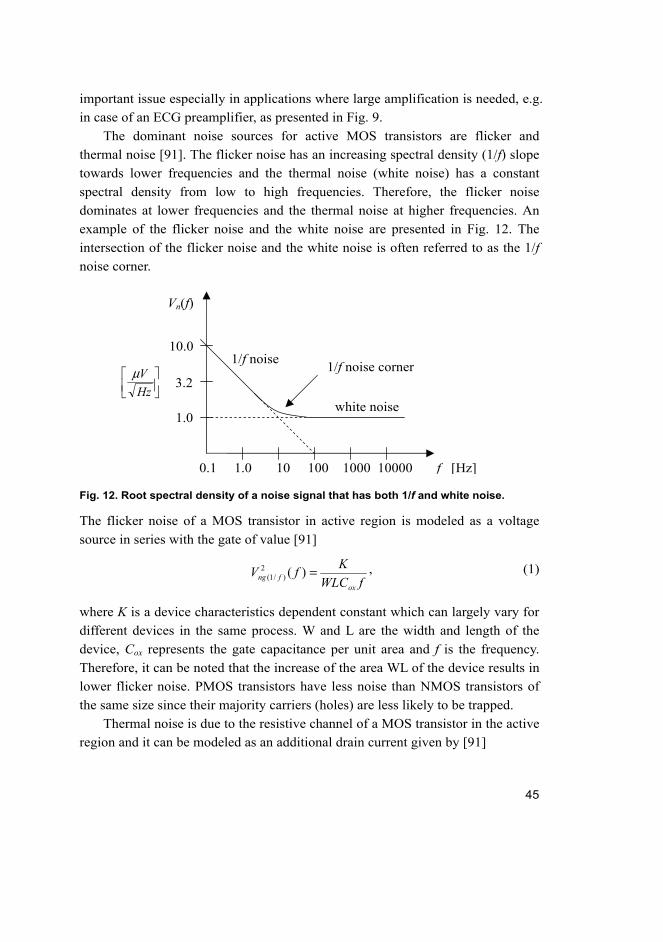
45
important issue especially in applications where large amplification is needed, e.g.
in case of an ECG preamplifier, as presented in Fig. 9.
The dominant noise sources for active MOS transistors are flicker and
thermal noise [91]. The flicker noise has an increasing spectral density (1/f) slope
towards lower frequencies and the thermal noise (white noise) has a constant
spectral density from low to high frequencies. Therefore, the flicker noise
dominates at lower frequencies and the thermal noise at higher frequencies. An
example of the flicker noise and the white noise are presented in Fig. 12. The
intersection of the flicker noise and the white noise is often referred to as the 1/f
noise corner.
Fig. 12. Root spectral density of a noise signal that has both 1/f and white noise.
The flicker noise of a MOS transistor in active region is modeled as a voltage
source in series with the gate of value [91]
fWLC
KfV
oxfng =)(2
)/1(, (1)
where K is a device characteristics dependent constant which can largely vary for
different devices in the same process. W and L are the width and length of the
device, Cox represents the gate capacitance per unit area and f is the frequency.
Therefore, it can be noted that the increase of the area WL of the device results in
lower flicker noise. PMOS transistors have less noise than NMOS transistors of
the same size since their majority carriers (holes) are less likely to be trapped.
Thermal noise is due to the resistive channel of a MOS transistor in the active
region and it can be modeled as an additional drain current given by [91]
1/f noise
white noise
1/f noise corner
1.0
10.0
3.2
0.1 1.0 10 100 1000 10000 f [Hz]
Vn(f)
Hz
Vμ
46
mTnd gkTfI
=
3
24)(2
)(, (2)
where k is the Boltzmann’s constant, T is the absolute temperature and gm the
transconductance of the transistor. The current noise source is normally added in
parallel with the channel of the transistor, but sometimes the noise analysis can be
simplified by replacing the current noise source with an equivalent input noise
voltage source, which would cause the same drain current noise for the transistor.
Then the total input referred noise (IRN) voltage in series with the gate would be
fWLC
K
gkTfV
oxmni +
= 1
3
24)(2 . (3)
This simplified model is valid for low and moderate frequencies since it assumes
that the gate current is zero. At higher frequencies, an appreciable amount of
current will flow through the gate-capacitance CGS, which causes this model to be
inaccurate. According to (3) the IRN can be minimized by choosing large gm and
area for a transistor. In opamps, the inherent noise is dominated by the input
differential pair and its active load transistors, which need to be noise optimized
when aiming for desired noise performance for the whole amplifier.
Distortion is caused by the nonlinearities of a circuit. Most often the
dominating type of distortion is harmonic distortion. If the input signal is a sine
signal with a fundamental frequency of f1, the harmonic distortion appears at the
output spectrum as additional frequency components, which are multiples of the
fundamental frequency, i.e. 2f1, 3f1, 4f1… etc. Typically these components will
rise up quickly when the signal level exceeds the linear operating range of the
circuit. Therefore, it is also important to maximize the linear operating range of
the circuit with respect to the supply voltages, when aiming for the maximum DR
for the circuit.
In opamps, the DR limitation is usually caused by the common-mode voltage
range Vin,CMR of the input stage. Depending on the feedback configuration, the
requirements for the input stage may vary greatly. The most often used feedback
configurations and their input stage requirements are shown in Fig. 13. The output
stages of the opamps are assumed to operate with the full scale of supply voltages,
i.e. rail-to-rail, and the output DC voltage is therefore set at mid-supply (VDD/2).
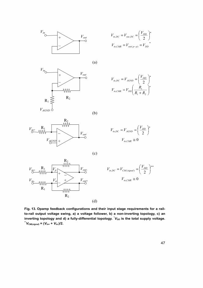
47
Fig. 13. Opamp feedback configurations and their input stage requirements for a rail-
to-rail output voltage swing, a) a voltage follower, b) a non-inverting topology, c) an
inverting topology and d) a fully-differential topology. *VDD is the total supply voltage. **VCM(signal) = (Vin+ + Vin-)/2.
(a)
==
2,,DD
DCoutDCin
VVV
*
DDppoutCMRin VVV == − )(,
*
==
2,DD
AGNDDCin
VVV
*
+
=21
1, RR
RVV DDCMRin
*
==
2,DD
AGNDDCin
VVV
*
0, ≅CMRinV
(c)
(b)
+
_
Vin Vout
==
2)(,DD
signalCMDCin
VVV
**
0, ≅CMRinV
+_
VAGND
Vin
R2 R1
Vout
Vout _
+
Vin+
VAGND
R2
R1
+
_
Vin+ Vp Vout-
Vout+ Vin- Vn +
_
R2
R1
R2
R1
(d)
48
The largest input voltage swing requirements are set by the first two feedback
configurations in Fig. 13, namely the voltage follower and the non-inverting
topology. Because the input and output voltages of the voltage follower are the
same, the input stage also has to be able to process rail-to-rail signals. The input
signal swing requirements for the non-inverting topology are relieved by a
feedback factor β = R1/(R1 + R2), which inversely defines the amplification from
the input to the output. With both of these topologies it is important to set the
input DC voltage Vin,DC or the analogue ground voltage VAGND to mid-supply
(VDD/2), otherwise the maximum linear voltage swing at the output is limited.
The last two topologies in Fig. 13 are the inverting and the fully-differential
(FD) topology. With these feedback topologies the Vin,CMR at the inputs of the
opamp is close to zero. This is due to a virtual short between the positive and the
negative input terminals of the opamp. With the inverting topology the analogue
ground voltage VAGND has to be set again to VDD/2 in order to reach a rail-to-rail
output swing for the amplifier. In the case of the FD amplifier, the Vin,DC is
determined by both the output DC voltage (VDD/2), which is set by the opamp’s
own common-mode feedback (CMFB) circuit, and the VCM(signal), i.e. the signal
ground, which is defined by the signal source or the CMFB circuit of a previous
output stage. VCM(signal) has to be equal to VDD/2 in order to avoid DC currents
between the input and output terminals of the FD opamp.
From the input stage requirements listed in Fig. 13 it can be concluded that
for rail-to-rail output operation all feedback configurations need the Vin,CMR to be
set around VDD/2. Depending on the feedback configuration, the input voltage
swing can vary from close to zero to rail-to-rail. The next sub-chapter will show
how these input and output voltage requirements are met with conventional
input/output stages in an LV/LP environment.
4.1.1 Conventional input/output stages
A conventional NMOS-type input stage for an opamp is presented in Fig. 14 (a).
It consists of a differential input transistor pair M2 – M3 with an active load M4 –
M5 provided with a bias current via M1. The minimum supply voltage VDD(min) for
the NMOS-type differential input stage is limited either by three saturation
voltages of M1, M2 and M4 (or M1, M3 and M5) or by the minimum voltage
requirement for the input transistors M2 and M3, whichever is higher, i.e.
49
Fig. 14. Input/output common-mode (CM) voltage range of (a) an NMOS- and (b) a
PMOS-type input stage.
2)(1)(4)(2)(1(min) ,max GSsatDSsatSDsatDSsatDSDD VVVVVV +++=
)()( 2,3max satDSTsatDS VVV +≈ TV2≤ , (4)
and for the PMOS-type input stage, Fig. 14 (b):
2)(1)(4)(2)(1(min) ,max SGsatSDsatDSsatSDsatSDDD VVVVVV +++=
)()( 2,3max satDSTsatDS VVV +≈ TV2≤ , (5)
where VGS (VSG for PMOS) is the gate-to-source voltage, VDS(sat) (VSD(sat) for
PMOS) the drain-to-source saturation voltage of an NMOS transistor and VT the
threshold voltage of a MOS transistor. If the threshold voltages and the saturation
voltages of NMOS- and PMOS-transistors are assumed to be the same, i.e.
VT(NMOS) = |VT(PMOS)| and VDS(sat,NMOS) = VSD(sat,PMOS), then (4) and (5) can be
Vin+ Vin-
Vout- Vout+
VB1
VB2 M1
M2 M3
M4 M5
VDD VDD = 3 V
VDD = 1 V
Vin,CMR Vout,CMR
Vin,CMR Vout,CMR
(a)
(b)
VDD = 1 V
Vin,CMR Vout,CMR
Vin,CMR
Vout,CMR Vin+ Vin-
Vout+
VB1
VB2
M1
M2 M3
M4 M5
VDD = 3 V VDD
Vout-

50
simplified to be either equal to the sum of three saturation voltages or the sum of
one threshold voltage and two saturation voltages, whichever is higher. With
typical values for VDS(sat) and VT, the minimum supply voltage can also be
approximated to be equal to or less than two threshold voltages of a MOS
transistor. This complies well with the minimum supply voltage requirement for
digital circuits.
The input CMR of the NMOS input stage is limited from the lower end to
2)(1(min), GSsatDSCMin VVV +=
TsatDS VV +≈ )(2 (6)
and from the upper end to
2)(2)(4(max), GSsatDSsatSDDDCMin VVVVV +−−=
2)(4 TsatSDDD VVV +−= , (7)
which even exceeds the supply voltage. For the PMOS input stage, the lower limit
appears at
2)(2)(4(min), SGsatSDsatDSCMin VVVV −+=
2)(4 TsatDS VV −= , (8)
which is less than the negative supply voltage (ground), and the upper limit at
2)(1(max), SGsatSDDDCMin VVVV −−=
TsatDSDD VVV −−≈ )(2 . (9)
From (4) – (9) it can be concluded that the input CMR for both types of input
stage is approximately zero when the supply voltage is set to the minimum. If VT
is assumed to be 0.5 V and VDS(sat) between 100 mV and 200 mV, the minimum
supply voltage for a conventional input stage is about 0.7 V – 0.9 V. Fig. 14 also
shows the location of the input CMR in two different cases where the supply
voltage is either 3 V or 1 V. In the latter case, the input CMR is very narrow and
does not reach the mid-supply, which might be a problem depending on the
feedback configuration (see Fig. 13) and the desired output CMR for the whole
opamp.
The output CMRs of the input stages shown in Fig. 14 are limited by the
three drain-to-source saturation voltages of the stacked transistors. Therefore, the
output CMR for the amplifier presented in Fig. 14 (a) is
51
)()(2)(1(min), 2 satDSsatDSsatDSCMout VVVV =+= (10)
)(4(max), satSDDDCMout VVV −= (11)
and for the amplifier in Fig. 14 (b)
)(4(min), satDSCMout VV = (12)
)()(2)(1(max), 2 satSDDDsatSDsatSDDDCMout VVVVVV −=−−= . (13)
Because the gain of the discussed 1-stage amplifiers is quite low, they are
normally equipped with one or more output stages. The most commonly used
output stage for an opamp is a common-source topology, as shown in Fig. 15. The
Fig. 15. Input/output voltage range for a common-source amplifier.
common-source topology is also the most promising choice for a low-voltage
output stage, since it provides rail-to-rail output swing (separated by only one
VDS(sat) from both supply rails) down to very low supply voltages. The minimum
supply voltage for the common-source amplifier is limited by one VGS (added
with the input voltage swing of transistor M1), i.e.
)(111(min) satDSTGSDD VVVV +== , (14)
which assumes that one VSG (= VGS) is also enough to bias transistor M2. The input signal range is limited from the lower end to
1)(11(min) TsatDSGSin VVVV +== (15)
and from the upper end to
1)(1)(2(max) GSsatDSsatSDDDin VVVVV +−−=
1)(2 TsatSDDD VVV +−≈ , (16)
VDD = 3 V
VDD = 1 V
Vout Vin
Vout Vin
Vout Vin
VB
VDD
M1
M2

52
which implies that the input voltage range can even exceed the positive supply
rail. The input transistor in Fig. 15 is of NMOS-type. An inverse topology is
obtained if terminals Vin and VB are exchanged. Then the input voltage range is
shifted close to the negative supply rail, while the output range still remains rail-
to-rail.
The presented input and output stages can be combined in several ways. Fig.
16 shows two traditional topologies, which are the single-ended (SE) and the
Fig. 16. (a) Single-ended Miller-compensated 2-stage operational amplifier (OPA) and
(b) a fully-differential OPA (CMFB circuit is not shown).
fully-differential (FD) versions of a Miller-compensated 2-stage operational
amplifier (OPA). For simplicity, only topologies with a PMOS-type input stage
are shown. The minimum supply voltage requirement for the SE OPA in Fig. 16
(a) is
2)(14)(2)(1(min) ,max SGsatSDGSsatSDsatSDDD VVVVVV +++=
)(3 satDST VV +≈ , (17)
which is one VDS(sat) higher than shown for topologies in Fig. 14. This is due to the
diode connected current mirror load transistors M4 and M5 of the input stage. The
minimum supply voltage requirement for the FD OPA in Fig. 16 (b) is
2)(16)(2)(1(min) ,max SGsatSDGSsatSDsatSDDD VVVVVV +++=
)(3 satDST VV +≈ , (18)
which is the same as for the SE OPA. This is due to the output transistors M6 and
M7 of the FD OPA. The input stage alone (which is similar to the input stage in
Vout+ Vin- Vin+ Vout
VB1
CM
M1
M2 M3
M4 M5 M6
M7
VDD
Vin- Vin+
VB1
CM
M1
M2 M3
M6 M4 M5 M7
VDD
M9
Vout-
CM
M8
VB2
(a) (b)
53
Fig. 14 (b)) would be capable of operating with the minimum supply voltage
given by (5) but since the drain-to-source voltage of M4 is at the same time the
gate-to-source voltage of M6, i.e. VDS4 = VGS6 (and VDS5 = VGS7) then the whole
amplifier needs the same supply voltage as its SE version.
When aiming for a lower supply voltage than that set by (17) and (18), the
input stage of an SE OPA can be constructed as in Fig. 17 (a) [106]. This topology
employs an additional folded structure (M8 – M11) to reduce the voltage drop
across the current mirror transistors (M4 – M5). A fully-differential version of the
Fig. 17. (a) Single-ended operational amplifier (OPA) and (b) a fully-differential OPA
with folded input stage structures (CMFB circuit not shown) [106] © 1995 IEEE.
Vin- Vin+ Vout
VB1
CM
M1
M2 M3
M5 M6
VDD
M10
VB2 VB2
M4
M7 M8
M9 M11
(a)
(b)
VB1
Vout- Vin- Vin+ CM
M1
M2 M3
M5 M6
VDD
M10
VB2 VB2
M4
M7 M8
M9 M11 VB3
M12
M13
Vout-
CM

54
OPA with the folded input stage structure is presented in Fig. 17 (b) [106]. The
minimum supply voltage requirement for these SE and FD OPAs is now
2)(1)(4)(2)(1(min) ,max SGsatSDsatDSsatSDsatSDDD VVVVVV +++=
)(2 satDST VV +≈ , (19)
which is one VDS(sat) lower that the VDD(min) presented in (17) for topologies in Fig.
16. With both versions, the folded structure (M8 – M11) also helps to keep both
input and load transistors (M2 – M5) in the saturation region in all conditions.
The main problem with all presented opamps and their input stages with low
supply voltages is that their input common-mode (CM) voltage range does not
reach the mid-supply, which is required for rail-to-rail output operation with all
feedback configurations shown in Fig. 13. Another problem related to the
differential topology is that it needs a CMFB circuit, which has to process the
whole rail-to-rail output signal range. Traditional input stages of CMFB circuits
[107] have been designed using structures similar to the input stages used for the
opamps, which are not directly usable for low supply voltages.
One possible continuous-time (CT) solution is to use a passive level-shifter
R1 – R3, shown in Fig. 18 [106], at the input of a 5-transistor CMFB circuit. If the
output CM signal of the opamp is set to mid-supply (VCM = Vout+ = Vout- = VDD/2),
then the component values for R1 – R3 and the reference voltage can be selected
from the following relationship:
321
3)( ||2 RRR
RVVV DD
REFCMFBin +⋅== . (20)
Fig. 18. Fully-differential OPA with a passive level-shifter at the input of a CMFB circuit
presented in [106] © 1995 IEEE.
Vin+ Vout-
Vin- Vout+
VBIAS
VDD
VREF
Vctrl
+ _
_ + R2
R3
R1
Vin(CMFB)
55
As can be seen from (20), there is a trade-off between the amount of CM signal
present at the input of the CMFB circuit and the amount of level shift. Low VREF
allows the use of low supply voltage, but at the expense of reduced CM gain in
the CMFB loop. Another drawback is an additional direct current path from the
outputs of the opamp to ground. Resistors should be avoided in low-power
designs, since they add either power consumption or area (or both) to the circuit.
Furthermore, the differential-mode gain of the amplifier is largely reduced with
practical values for integrated resistors.
Another recent CT solution for a CT CMFB circuit (Fig. 19) is presented in
[108]. It consists of two source-coupled differential pairs connected on top of
each other. Since the conductivity of equally sized N- and PMOS transistors is
different, the width-to-length ratios (W/L)N and (W/L)P have to be carefully
selected in order to minimize the CMFB circuit’s gain to differential mode signals.
This circuit features quite linear rail-to-rail operation even with very low supply
voltages, but its current consumption increases dramatically with supply voltages
larger than ~2VT.
Fig. 19. Continuous-time CMFB circuit presented in [108] © 2008 IEEE.
One possible solution for a CMFB circuit is also to use a discrete-time (DT)
structure based on the switched-capacitor (SC) technique. DT solutions will be
discussed in Chapter 4.3 in the context of switched-opamps.
There are several ways presented in the literature to overcome the problems
caused by the difference between the input and the output common-mode range
(CMR) of an opamp. Traditionally, symmetrical input CMR around mid-supply
has been achieved by connecting an NMOS- and a PMOS-type input stage in
parallel configuration [109], which combines the CMR of both input stages
resulting in rail-to-rail input CMR. This arrangement works fine when the supply
VDD
Vout Vin2 Vin1
M1 M2
M3 M4
56
voltage is higher than the sum of the input CMR of both stages. When the supply
voltage is very low, there will be a gap between the CMRs of the NMOS- and
PMOS-input stages around the mid-supply. The gap can be removed by using
either level-shifting technique [110] (bipolar) or [111] (CMOS) but this is
achieved at the expense of increased power consumption due to additional biasing
circuitry.
Another way to match the input and output CMRs of an opamp is to add a
floating battery in front of the input stage [112, 113] (continuous-time), which is
based on a voltage drop across a resistor with a fixed bias current or [114]
(discrete-time), which uses a switched-capacitor circuit for the same task. Again,
in the former case, an additional bias circuitry increases the total current
consumption, while in the latter case, the switched-capacitor (SC) circuit suffers
from a limited input voltage swing (if a clock-booster is not used) and injects
noise onto the signal path due to clock feed-through.
One possible way to adjust the input CMR of an opamp in a fully-differential
resistive feedback configuration (Fig. 13 (d)) is to use an input CMFB circuit
[115], which sets the input CMR of the opamp regardless of the input signal or
the output CMR of the opamp. This is achieved with additional current sinks or
sources connected to the input terminals of an opamp, which in turn causes the
CM voltage at the input terminals to be shifted upwards or downwards depending
on the selected direction of the current. Naturally, the total current consumption
increases due to the additional current sinks or sources connected to the input.
The input CMR of an opamp can also be enhanced by using special low-
voltage devices, such as low-threshold voltage (low-VT) transistors [61, 115-118],
which requires a special process. Another way is to use floating-gate (FG) [119-
124], quasi-floating-gate (QFG) [125-127], dynamic threshold MOS (DTMOS)
[128-130] or bulk-driven (BD) transistors [131-133] instead of conventional
transistors as an input differential pair. These devices are very interesting because
they can be used as replacements of conventional input transistors even without
the need for any additional bias circuits or process steps.
Since the rail-to-rail input/output CMR capability of an opamp is a desired
feature for both the ECG preamplifier of a heart rate detector and the RC
oscillator developed in this work, the properties of the input stages based on FG
and BD transistors are discussed in more detail within the next two sections.
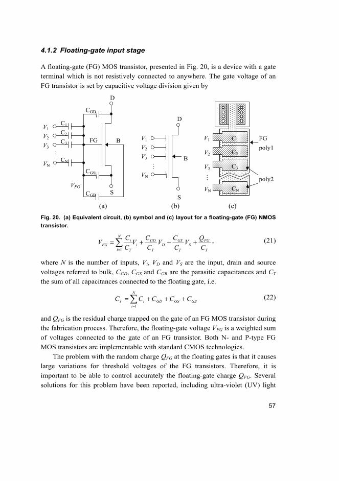
57
4.1.2 Floating-gate input stage
A floating-gate (FG) MOS transistor, presented in Fig. 20, is a device with a gate
terminal which is not resistively connected to anywhere. The gate voltage of an
FG transistor is set by capacitive voltage division given by
Fig. 20. (a) Equivalent circuit, (b) symbol and (c) layout for a floating-gate (FG) NMOS
transistor.
T
FGS
T
GSD
T
GDi
N
i T
iFG C
QV
C
CV
C
CV
C
CV +++=
=1
, (21)
where N is the number of inputs, Vi, VD and VS are the input, drain and source
voltages referred to bulk, CGD, CGS and CGB are the parasitic capacitances and CT
the sum of all capacitances connected to the floating gate, i.e.
GBGSGD
N
iiT CCCCC +++=
=1
(22)
and QFG is the residual charge trapped on the gate of an FG MOS transistor during
the fabrication process. Therefore, the floating-gate voltage VFG is a weighted sum
of voltages connected to the gate of an FG transistor. Both N- and P-type FG
MOS transistors are implementable with standard CMOS technologies.
The problem with the random charge QFG at the floating gates is that it causes
large variations for threshold voltages of the FG transistors. Therefore, it is
important to be able to control accurately the floating-gate charge QFG. Several
solutions for this problem have been reported, including ultra-violet (UV) light
V1
V2
V3
VN
…
D
B
S
V1
V2
C1
C2
FG
poly1
poly2
V3
VN
C3
CN
…
D
V1
V2
V3
VN
C1
C2
C3
CN
CGD
CGS
CGB
VFG
B
S
…
FG
(a) (b) (c)
58
irradiation [124, 134], the use of the Fowler-Nordheim tunneling effect and hot
electron injection [135-137], forcing an initial condition with a switch [138] and
taking advantage of the fabrication processing steps themselves [139]. The first
solution sometimes gives acceptable results, but it requires removal of the
passivation mask if it reflects UV light. This is not a standard procedure and
might compromise the reliability of the chip in the long run. The second solution
requires extra circuitry and high voltages which are not compatible with LV
technologies. The third solution leads to quasi-floating-gate (QFG) operation
since the DC voltage at the floating-gate is no longer adjustable with the input
capacitors and their input voltages, but instead, will slowly drift towards the
substrate voltage of the closed switch due to its leakage current. The fourth
solution is the most recently reported technique to remove random charge from
the floating gates of FG circuits. In this technique the floating gates, which are on
a poly1 layer, are contacted to the uppermost metal layer. After depositing the
uppermost metal layer in a fabrication process, all parts of the chip which are
contacted to that metal layer are temporarily connected together, which means
that the charge trapped on the floating gates flows to other parts of the chip. If the
substrate of the chip is also contacted to the uppermost metal layer, the floating
gates are discharged to the substrate. After etching of the uppermost metal layer,
the floating nature of the gates is restored.
FG transistors have been used earlier only in digital electronics, where they
form the basis of EEPROM devices [140]. During the last few years FG
transistors have also started to attract interest in analogue LV/LP circuit design.
This is due to the fact that the input voltage range of an FG MOS can even be
extended below its threshold voltage. This feature can be exploited also in the
design of opamps.
An example of an input stage for an opamp implemented with an FG input
differential pair is presented in Fig. 21. Although both NMOS- and PMOS-type
input stages are realizable in a standard CMOS process, a PMOS-type input stage
has been chosen as an example. The minimum supply voltage requirement
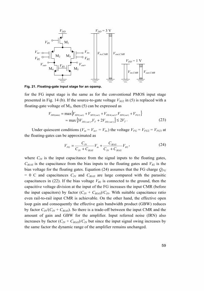
59
Fig. 21. Floating-gate input stage for an opamp.
for the FG input stage is the same as for the conventional PMOS input stage
presented in Fig. 14 (b). If the source-to-gate voltage VSG2 in (5) is replaced with a
floating-gate voltage of M2, then (5) can be expressed as
2)(1)(4)(2)(1(min) ,max FGsatSDsatDSsatSDsatSDDD VVVVVV +++=
)()( 2,3max satDSTsatDS VVV +≈ TV2≤ . (23)
Under quiescent conditions (Vin = Vin+ = Vin-) the voltage VFG = VFG2 = VFG3 at
the floating-gates can be approximated as
2BBIASIN
BIASin
BIASIN
INFG V
CC
CV
CC
CV
++
+= , (24)
where CIN is the input capacitance from the signal inputs to the floating gates,
CBIAS is the capacitance from the bias inputs to the floating gates and VB2 is the
bias voltage for the floating gates. Equation (24) assumes that the FG charge QFG
= 0 C and capacitances CIN and CBIAS are large compared with the parasitic
capacitances in (22). If the bias voltage VB2 is connected to the ground, then the
capacitive voltage division at the input of the FG increases the input CMR (before
the input capacitors) by factor (CIN + CBIAS)/CIN. With suitable capacitance ratio
even rail-to-rail input CMR is achievable. On the other hand, the effective open
loop gain and consequently the effective gain bandwidth product (GBW) reduces
by factor CIN/(CIN + CBIAS). So there is a trade-off between the input CMR and the
amount of gain and GBW for the amplifier. Input referred noise (IRN) also
increases by factor (CIN + CBIAS)/CIN but since the input signal swing increases by
the same factor the dynamic range of the amplifier remains unchanged.
M4 M5
VDD = 1 V
Vout,CMR
Vin,CMR Vout,CMR Vin+ Vin-
Vout- Vout+
VB1
VB3
M1
M2 M3
VDD
Vin,CMR
VB2 VB2
VDD = 3 V
60
4.1.3 Bulk-driven input stage
A bulk-driven (BD) MOS transistor with its associated parasitic components is
presented in Fig. 22. A BD MOS transistor is a device with five terminals, namely
gate, source, drain, bulk and substrate (usually ground). The bulk terminal is the
transistors’ local substrate, i.e. n- or p-well. Therefore only n- or p-type of BD
MOS is available in a standard CMOS process depending on the type of the
substrate. The BD PMOS presented in Fig. 22 assumes an n-well process
technology where p-type substrate is used.
Fig. 22. (a) Equivalent circuit and (b) symbol for a bulk-driven PMOS transistor.
The input signal is applied to the bulk terminal of the BD PMOS while the gate
terminal is connected to a suitable bias voltage (normally ground) to turn on the
transistor (VBIAS = VSG ≥ |VT| + VSD(sat)). As a result, the BD PMOS can operate
with both positive and (slightly) negative input voltages (Vin = VBS), which is
comparable to operation of a depletion-mode device. In order to avoid turning on
the parasitic bipolar junction transistor (BJT) in parallel with the BD PMOS in
Fig. 22, the forward bias voltage VSB of the source-to-bulk p-n junction can be
only a few hundred millivolts. If the threshold voltage of the parasitic BJT is
exceeded, then a considerable part of the source-current will flow through the
parasitic BJT from source to bulk (input), drain and substrate.
The drawbacks of a BD MOS transistor compared to a normal gate-driven
MOS transistor of the same size are smaller transconductance (gmb instead of gm)
because of smaller control capacitance of the depletion layer, lower transition
frequency fT because of larger capacitance to the substrate and higher IRN
S
B G
D
S
CGS
Vin
D
B
VBIAS
CGD
CBS
CBD
CBSUB
G
(a) (b)
61
because of smaller transconductance. These drawbacks, though, can be
compensated to some extent by resizing the device or increasing the bias current.
A BD PMOS input stage for an opamp is presented in Fig. 23. The only
difference between the BD PMOS and the conventional PMOS input stage
presented in Fig. 14 (b) is that the input signal is applied to the bulk terminals
instead of the gate terminals and the gate terminals are connected to a suitable
bias voltage VB2 (usually ground) to turn on the input transistors.
Fig. 23. Bulk-driven input stage for an opamp.
The minimum supply voltage requirement for the BD PMOS input stage is the
same (5) as for the conventional PMOS input stage, but the input CM voltage
range is much larger. This is due to the fact that the threshold voltage limitation of
the input transistors M2 and M3 is no longer on the signal path. With very low
supply voltages the input CMR can easily be rail-to-rail. With larger supply
voltages the maximum input CM voltage can reach the positive supply, but the
minimum input CM voltage may be limited because of the parasitic BJT in
parallel with the input transistors. Therefore, the bias point of the input transistors
has to be carefully designed and verified by circuit simulations when aiming for
rail-to-rail input CMR.
4.2 Switches
Since the analogue signal processing (ASP) block for a QRS detector, presented
in Fig. 9 (Chapter 2.3), is implemented using SC techniques, this chapter points
out the problems of an analogue switch under low-voltage (LV) conditions and
introduces some existing solutions for these problems.
VDD = 3 V VDD
M2 M3 VDD = 1 V
Vin,CMR Vout,CMR
Vin,CMR Vout,CMR Vin+ Vin-
Vout- Vout+
VB1
VB3
M1
M4 M5
VB2
62
There are basically three types of switches available in standard CMOS
processes. Two of them are based on using only one transistor, i.e. NMOS or
PMOS, and the third one is a complementary MOS (CMOS) switch, which
combines an NMOS and a PMOS transistor in parallel configuration. The
switches and their conductance as a function of the terminal voltage VX (either V1
or V2) under two different supply voltages are presented in Fig. 24.
Fig. 24. Symbols for (a) NMOS- (b), PMOS- and (c) CMOS-type switches and their
conductance as a function of the terminal voltage VX with supply voltages of (d) VDD =
3 V and (e) VDD = 1 V, assuming VTN = VTP = 0.5 V.
The conductance gds of a MOS switch depends on sizing and the overdrive
voltage of the switch. The overdrive voltage is the voltage headroom above the
threshold voltage of the switch. In case of an NMOS switch, conduction is
possible when its gate terminal is switched to the positive supply voltage and the
voltage VX is at least one threshold voltage VTN below the supply voltage. The
NMOS switch is turned off irrespective of the voltage VX (assuming that VX is
limited between the supply rails) by switching the gate terminal to the ground. A
φ
V1
(a)
gds
VX VTP VDD – VTN VDD
NMOS PMOS
VDD = 3 V
CMOS
gds
VX VTP,
VDD - VTN
VDD
NMOS PMOS
VDD = 1 V
CMOS
V2
φ
V1 V2
(b)
(d) (e)
φ
(c)
V1 V2
φ
63
PMOS switch conducts when its gate terminal is switched to the ground and the
voltage VX is at least one threshold voltage VTP higher than the ground voltage.
Similarly, the PMOS switch is turned off by switching its gate terminal to the
positive supply voltage. A CMOS switch combines the operating regions of an
NMOS and a PMOS switch as can be seen from Fig. 24 (d). The conductance of
equally sized NMOS and PMOS transistors with the same overdrive voltage are
different because of different mobility of majority charge carriers, i.e. electrons
and holes in NMOS and PMOS transistors, respectively. When the supply voltage
drops to 1 V, which in the case of Fig. 24 (e) is the sum of the threshold voltages
of the NMOS and the PMOS transistors (VDD = VTN + VTP ≈ 2VT), the conductance
for VX around the mid-supply drops to zero, i.e. both transistors are turned off.
In digital circuits the supply voltage can be even lower than 2VT because the
input signal VX for a digital switch is either logical “0” or “1”, i.e. close to ground
voltage or VDD. Therefore, the minimum supply voltage for a digital switch can be
as low as
ovTdigitalDD VVV +=)(min,, (25)
where VT is the threshold voltage of an NMOS or a PMOS transistor and Vov is the
minimum overdrive voltage to meet the speed specifications (i.e. the minimum
conductance).
In analogue circuits the situation is different because an analogue switch has
to conduct the whole signal swing, which can even be rail-to-rail. A rail-to-rail
operation requires that the DC voltage level of the signal is set to VDD/2. Because
the switch has to conduct both positive and negative signals with respect to VDD/2,
the minimum supply voltage for a rail-to-rail analogue CMOS switch is limited to
ovTueanaDD VVV += 2)log(min,. (26)
One solution for lowering the supply voltage below (26) is to move the CM
voltage from the mid-supply closer to one of the supply voltages and use only one
type of switch, i.e. NMOS or PMOS. Unfortunately, this solution limits the
maximum signal swing to less than a half of the total supply voltage, which also
reduces the SNR and the maximum possible DR of the circuit. Other solutions are
the use of 1) low-VT devices [61, 115-118], 2) internal voltage multipliers (clock-
boosters) [141-144] or 3) bootstrap technique [145-150]. Low-VT devices are not
available in standard CMOS process technologies and clock-boosters cannot be
used with advanced LV CMOS process technologies due to the maximum supply
64
voltage limitation and the risk of damaging the thin gate oxide of the switch
transistors with too large terminal voltages, i.e. VGS, VGD or VDS > VDD.
The bootstrap technique is an interesting alternative for clock-boosters since
it uses a signal-independent switching voltage VGS = VDD to drive the switch.
Therefore, none of the voltages VGS, VGD or VDS are likely to exceed the VDD,
which should protect the switch transistor from overstress [145]. Fig. 25 shows
the operation principle and the waveforms of a bootstrapped MOS switch.
Because the VGS during the active phase of the switch is always equal to VDD, it
not only provides a rail-to-rail input signal capability, but also a constant switch
conductance, which reduces the signal-dependent nonlinearity present in
conventional switches.
Fig. 25. (a) Bootstrapped MOS switch and (b) its conceptual waveforms.
Although the bootstrapped switch provides many desired features, such as rail-to-
rail input capability and reduced signal-dependent switch nonlinearity, it also
needs quite a complex and carefully dimensioned circuit layout implementation in
t
VDD
Vin
2VDD
VG
V bootstrapped
clock
VDD _
+
OFF ON (a)
(b)
65
order to not exceed the maximum ratings set for the terminal voltages, which
subject is studied more extensively in [145]. Fortunately, the problems of series
switches on the signal path can be largely avoided in SC circuits by the use of a
switched-opamp technique [151-163].
4.3 Switched-opamps
This chapter reviews a few switched-opamp (SO) topologies and shows how the
minimum supply voltage of traditional SC circuit blocks, like integrators, can be
lowered by replacing conventional opamps with switched-opamps. The first
subchapter explains the restrictions for the minimum supply voltage set by a
standard SC integrator topology and shows how these limitations can be relieved
by replacing it with different switched-opamp switched-capacitor (SO-SC)
integrator topologies. The second subchapter shows some internal circuit
structures for switched-opamps and gives one example of a fully-differential SO
topology which is capable of very low-voltage operation.
4.3.1 Switched-opamp integrators
The basic idea behind a switched-opamp [151] is presented in Fig. 26. Low-
voltage operation is achieved by replacing a CT opamp and a critical series switch
at its output with a switchable opamp. The opamp can be switched on and off, for
example, by switching its bias currents. Therefore, the switched-opamp can save
up to 50% of power consumption, which makes it a very attractive choice, not
only for LV applications, but for all LP designs.
The LV limitations of standard SC technique become clear by making
observations from a simple SC integrator topology, presented in Fig. 27. For rail-
Fig. 26. (a) Opamp with a switch at its output and (b) a switched-opamp.
Vin-
Vin+ +
_
Vout
φ
(a) (b)
Vin
Vin+
φ Vout
Critical
switch
+
_
66
Fig. 27. Standard switched-capacitor (SC) integrator topology.
to-rail operation VREF is assumed to be VDD/2 (VDD is the total supply voltage). If
the switches S1 – S4 are realized with CMOS switches, then the minimum supply
voltage for the SC integrator (limited by the switches) is
ovTDD VVV += 2(min), (27)
which is much higher than the VDD(min) for the LV opamps shown in Chapter 4.1.1.
It is possible to reduce the VDD(min) slightly by setting VREF closer to the other
supply voltage rail, e.g. ground, and replacing the CMOS switches with NMOS
switches, but this will also reduce the maximum available voltage swing, i.e. the
dynamic range (DR), at the outputs of the opamps. Since the switches S2 – S4 are
directly connected to VREF or to virtual ground, which is also at VREF, the
minimum voltage needed to drive these switches is now
ovTNREFS VVVV ++=(min)4,3,2. (28)
The minimum drive voltage for S1 is much larger because it has to handle the
whole output swing of the preceding opamp. Therefore, the drive voltage needed
for S1 is
ovTNppout
REFS VVV
VV +++= −
2)(1
(min)1, (29)
which makes switch S1 the most critical switch in the whole integrator structure.
As a result, the minimum supply voltage for this arrangement is
ovTNppoutsatDSDD VVVVV +++= − )(1)((min), (30)
_
+
C1
C3
C2
S1 S2
S3 S4
VREF
_
+
Overall
feedback
φ1
φ1
φ2
φ2
INT1 INT2
Critical
switch
67
where VDS(sat) is the linear output voltage range limitation of the first integrator
INT1, Vout1(p-p) the maximum output voltage swing of INT1, VTN the threshold
voltage of switch S1 and Vov the required overdrive voltage to turn on the switch.
If the first integrator INT1 and the critical switch S1 in Fig. 27 are replaced
with a switched-opamp presented in Fig. 26 (b) (such as in [151]), then the
minimum supply voltage is limited by the switches S2 – S4 and is the same as in
(28), i.e. VDD(min) = VS2,3,4(min). If VREF is assumed to be Vout1(p-p)/2 above the output
voltage limitation VDS(sat) of INT1, then VDD(min) can also be written as
ovTNppout
satDSDD VVV
VV +++= −
2)(1
)((min), (31)
which shows that the minimum supply voltage requirement is relieved by half of
the signal amplitude when compared to (30). The DR of the circuit is still limited
by one VGS = VTN + Vov below the supply voltage.
There is still another way to reduce the supply voltage of an SC integrator
even without the penalty of losing the rail-to-rail output capability of the opamps.
This solution is based on the use of level-shifters at the inputs of the switched-
opamps [152, 153]. A level-shifted version of an SO-SC integrator is presented in
Fig. 28. The idea behind this circuit is to combine the output voltage of the
integrator INT1 (Vout1 = VCM + Vsignal) with a constant DC voltage provided by the
level-shift capacitor CDC in order to set the desired input CM level for the next
integrator INT2. The level-shifted SO-SC integrator operates as follows: during
clock phase 1 (φ1), the output voltage of integrator INT1 is stored to C2. At the
same time, the charge stored in CDC is reset. During phase 2 (φ2), the charge in C2
is shared with CDC and fed forward to the next integrator INT2. If the output CM
voltage VCM of the first integrator is set to VDD/2 and the capacitor values are
chosen so that CDC = C2/2, then the input CM voltage of the integrator INT2 is set
at the negative supply voltage, i.e. ground, and all switches can be connected to
either VDD or ground. As a result, the minimum possible supply voltage for the
whole SO-SC integrator topology (excluding the limitations of opamps) is now
ovTNDD VVV +=(min). (32)
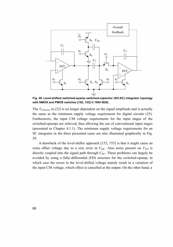
68
Fig. 28. Level-shifted switched-opamp switched-capacitor (SO-SC) integrator topology
with NMOS and PMOS switches [152, 153] © 1994 IEEE.
The VDD(min) in (32) is no longer dependent on the signal amplitude and is actually
the same as the minimum supply voltage requirement for digital circuits (25).
Furthermore, the input CM voltage requirements for the input stages of the
switched-opamps are relieved, thus allowing the use of conventional input stages
(presented in Chapter 4.1.1). The minimum supply voltage requirements for an
SC integrator in the three presented cases are also illustrated graphically in Fig.
29.
A drawback of the level-shifter approach [152, 153] is that it might cause an
extra offset voltage due to a size error in CDC. Also noise present on VDD is
directly coupled into the signal path through CDC. These problems can largely be
avoided by using a fully-differential (FD) structure for the switched-opamp, in
which case the errors in the level-shifted voltage mainly result in a variation of
the input CM voltage, which effect is cancelled at the output. On the other hand, a
_
+
C1
C3
C2
S1
S2
S3 S4
_
+
S6
S5
S7 φ1 φ1 φ2
φ2
φ2
φ1
φ2 CDC
INT1
INT2
Overall
feedback
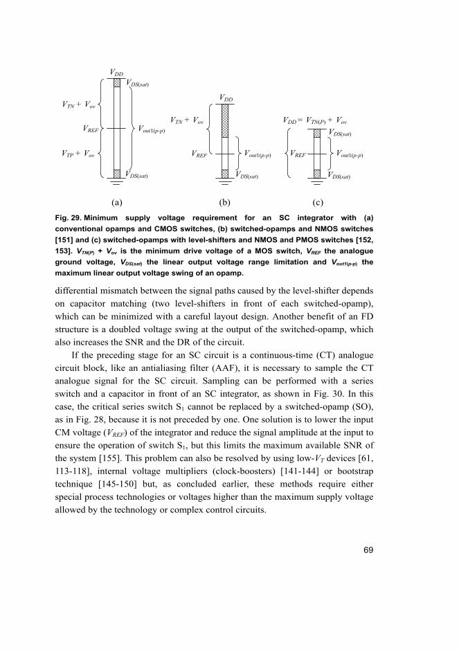
69
Fig. 29. Minimum supply voltage requirement for an SC integrator with (a)
conventional opamps and CMOS switches, (b) switched-opamps and NMOS switches
[151] and (c) switched-opamps with level-shifters and NMOS and PMOS switches [152,
153]. VTN(P) + Vov is the minimum drive voltage of a MOS switch, VREF the analogue
ground voltage, VDS(sat) the linear output voltage range limitation and Vout1(p-p) the
maximum linear output voltage swing of an opamp.
differential mismatch between the signal paths caused by the level-shifter depends
on capacitor matching (two level-shifters in front of each switched-opamp),
which can be minimized with a careful layout design. Another benefit of an FD
structure is a doubled voltage swing at the output of the switched-opamp, which
also increases the SNR and the DR of the circuit.
If the preceding stage for an SC circuit is a continuous-time (CT) analogue
circuit block, like an antialiasing filter (AAF), it is necessary to sample the CT
analogue signal for the SC circuit. Sampling can be performed with a series
switch and a capacitor in front of an SC integrator, as shown in Fig. 30. In this
case, the critical series switch S1 cannot be replaced by a switched-opamp (SO),
as in Fig. 28, because it is not preceded by one. One solution is to lower the input
CM voltage (VREF) of the integrator and reduce the signal amplitude at the input to
ensure the operation of switch S1, but this limits the maximum available SNR of
the system [155]. This problem can also be resolved by using low-VT devices [61,
113-118], internal voltage multipliers (clock-boosters) [141-144] or bootstrap
technique [145-150] but, as concluded earlier, these methods require either
special process technologies or voltages higher than the maximum supply voltage
allowed by the technology or complex control circuits.
(a) (b) (c)
VDS(sat)
Vout1(p-p)
VDD
VREF
VTN + Vov
VDS(sat)
Vout1(p-p)
VDD = VTN(P) + Vov
VREF
VDS(sat)
VDS(sat)
Vout1(p-p) VREF
VTN + Vov
VTP + Vov
VDD VDS(sat)
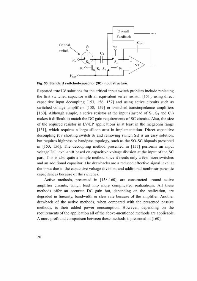
70
Fig. 30. Standard switched-capacitor (SC) input structure.
Reported true LV solutions for the critical input switch problem include replacing
the first switched capacitor with an equivalent series resistor [151], using direct
capacitive input decoupling [153, 156, 157] and using active circuits such as
switched-voltage amplifiers [158, 159] or switched-transimpedance amplifiers
[160]. Although simple, a series resistor at the input (instead of S1, S3 and CS)
makes it difficult to match the DC gain requirements of SC circuits. Also, the size
of the required resistor in LV/LP applications is at least in the megaohm range
[151], which requires a large silicon area in implementation. Direct capacitive
decoupling (by shorting switch S1 and removing switch S3) is an easy solution,
but requires highpass or bandpass topology, such as the SO-SC biquads presented
in [153, 156]. The decoupling method presented in [157] performs an input
voltage DC level-shift based on capacitive voltage division at the input of the SC
part. This is also quite a simple method since it needs only a few more switches
and an additional capacitor. The drawbacks are a reduced effective signal level at
the input due to the capacitive voltage division, and additional nonlinear parasitic
capacitances because of the switches.
Active methods, presented in [158-160], are constructed around active
amplifier circuits, which lead into more complicated realizations. All these
methods offer an accurate DC gain but, depending on the realization, are
degraded in linearity, bandwidth or slew rate because of the amplifier. Another
drawback of the active methods, when compared with the presented passive
methods, is their added power consumption. However, depending on the
requirements of the application all of the above-mentioned methods are applicable.
A more profound comparison between these methods is presented in [160].
_
+
CINT
CS
S1 S2
S3 S4
φ1
φ1
φ2
φ2
VREF
Vin
Critical
switch
Overall
Feedback
_
INT +
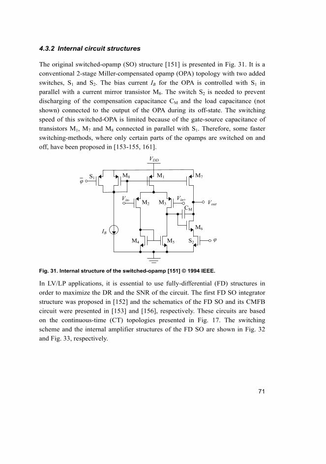
71
4.3.2 Internal circuit structures
The original switched-opamp (SO) structure [151] is presented in Fig. 31. It is a
conventional 2-stage Miller-compensated opamp (OPA) topology with two added
switches, S1 and S2. The bias current IB for the OPA is controlled with S1 in
parallel with a current mirror transistor M8. The switch S2 is needed to prevent
discharging of the compensation capacitance CM and the load capacitance (not
shown) connected to the output of the OPA during its off-state. The switching
speed of this switched-OPA is limited because of the gate-source capacitance of
transistors M1, M7 and M8 connected in parallel with S1. Therefore, some faster
switching-methods, where only certain parts of the opamps are switched on and
off, have been proposed in [153-155, 161].
Fig. 31. Internal structure of the switched-opamp [151] © 1994 IEEE.
In LV/LP applications, it is essential to use fully-differential (FD) structures in
order to maximize the DR and the SNR of the circuit. The first FD SO integrator
structure was proposed in [152] and the schematics of the FD SO and its CMFB
circuit were presented in [153] and [156], respectively. These circuits are based
on the continuous-time (CT) topologies presented in Fig. 17. The switching
scheme and the internal amplifier structures of the FD SO are shown in Fig. 32
and Fig. 33, respectively.
Vin- Vin+ Vout
IB
CM
M1
M2 M3
M4 M5 S2
VDD
M7
φ
φ
M6
M8 S1
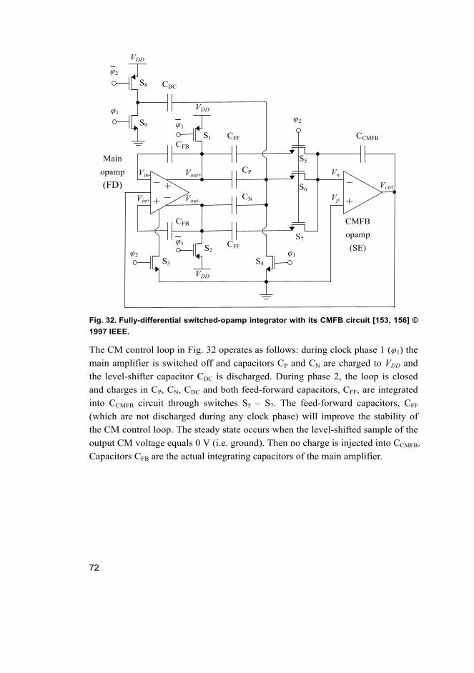
72
Fig. 32. Fully-differential switched-opamp integrator with its CMFB circuit [153, 156] ©
1997 IEEE.
The CM control loop in Fig. 32 operates as follows: during clock phase 1 (φ1) the
main amplifier is switched off and capacitors CP and CN are charged to VDD and
the level-shifter capacitor CDC is discharged. During phase 2, the loop is closed
and charges in CP, CN, CDC and both feed-forward capacitors, CFF, are integrated
into CCMFB circuit through switches S5 – S7. The feed-forward capacitors, CFF
(which are not discharged during any clock phase) will improve the stability of
the CM control loop. The steady state occurs when the level-shifted sample of the
output CM voltage equals 0 V (i.e. ground). Then no charge is injected into CCMFB.
Capacitors CFB are the actual integrating capacitors of the main amplifier.
Vin-
Vin+
Vout+
CFB
+
VDD
S2
φ2
φ2
S1
S3 S4
S5
S6
S7
S8
S9
VDD
VDD
Vout- + _
_
+
_
CFB
CCMFB
CDC
CFF
CFF
CP
CN
φ2
φ1
φ1
φ1
CMFB
opamp
(SE)
Main
opamp
(FD)
φ1
Vctrl
Vn
Vp
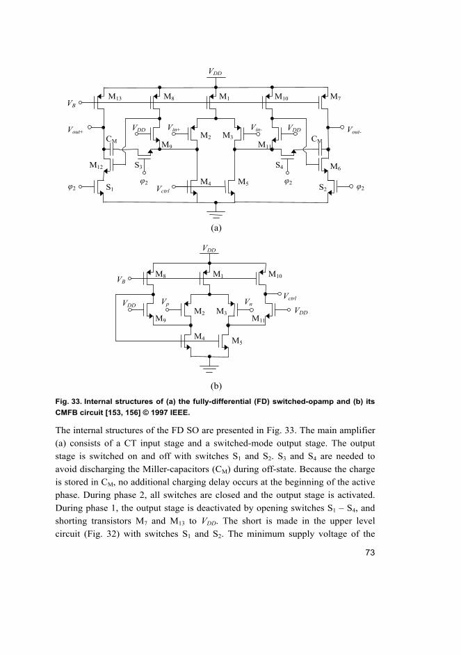
73
Fig. 33. Internal structures of (a) the fully-differential (FD) switched-opamp and (b) its
CMFB circuit [153, 156] © 1997 IEEE.
The internal structures of the FD SO are presented in Fig. 33. The main amplifier
(a) consists of a CT input stage and a switched-mode output stage. The output
stage is switched on and off with switches S1 and S2. S3 and S4 are needed to
avoid discharging the Miller-capacitors (CM) during off-state. Because the charge
is stored in CM, no additional charging delay occurs at the beginning of the active
phase. During phase 2, all switches are closed and the output stage is activated.
During phase 1, the output stage is deactivated by opening switches S1 – S4, and
shorting transistors M7 and M13 to VDD. The short is made in the upper level
circuit (Fig. 32) with switches S1 and S2. The minimum supply voltage of the
φ2 S2 S1
CM
φ2
CM
VB
Vin+ Vin- Vout+ Vout-
M1
M2 M3
M4 M5
M6
M7 M8
M9
M10
M11
M12
M13
VDD VDD
Vctrl
S3 S4
φ2 φ2
VDD
Vp Vn
M1
M2 M3
M4 M5
M8
M9
M10
M11 VDD
VDD Vctrl
VB
VDD
(a)
(b)
74
amplifier is not limited by the switches since S1 and S2 are connected to the
ground and S3 and S4 to nodes which are only one VDS(sat) above the ground.
Therefore, the minimum supply voltage for the main amplifier is the same as in
(19). Also the output swing remains almost rail-to-rail.
The CMFB circuit in Fig. 33 (b) is a CT 1-stage folded structure, similar to
the input stage of the main amplifier. The CM voltage of the CMFB circuit is
equal to ground and the output voltage Vctrl is connected to the gates of transistors
M4 and M5 in the main amplifier. The minimum supply voltage requirement is the
same as for the main amplifier.
Although most of the published LV/LP SOs are based on basic or folded-
input 2-stage Miller-compensated OPAs, shown in Fig. 31 and Fig. 33, it is also
possible to use operational transconductance amplifiers (OTAs), i.e. current-
mirror opamps [154, 155], Papers VI and VII or folded-cascode opamps [162,
163], as SOs. Folded-cascode opamps are not usually used in their basic form in
very LV applications due to their reduced output voltage swing caused by a
stacked-transistor structure needed at the output. For that reason, they are often
equipped with an additional common-source output stage (Fig. 15) in order to
achieve rail-to-rail output operation. Because all these types of SOs can be
designed to operate with supply voltages of less than ~2VT (i.e. VDD < VTN + |VTP|
≈ 2VT) they are very useful circuit blocks in both analogue and digital LV/LP
circuits, such as SC filters and ΣΔ ADCs.

75
5 Overview of the original papers
Papers I and II focus on developing continuous-time (CT), low-voltage (LV) and
low-power (LP) opamps with adequate input/output common-mode range (CMR)
and signal bandwidth (BW) to be used in amplifiers and filters aimed at
biomedical signal processing. Two different LV circuit design techniques, namely
the floating-gate (FG) and the bulk-driven (BD) technique, are revisited in the
design of two opamps with equal target specifications. A conventional 2-stage
Miller-compensated OPA is chosen as a starting point for these designs. The OPA
in Paper I is equipped with an FG input stage and the one in Paper II with a BD
input stage. Both opamps are processed on the same chip using standard 0.35 μm
n-well CMOS technology and they achieve almost rail-to-rail input/output CMR,
comparable gain, phase margin, GBW, slew-rate and noise properties with the
same power consumption. The performance of both opamps is considered to be
adequate for biosignal processing. However, the minimum supply voltage for the
FG OPA is 1.2 V while the BD OPA survives with 1 V. Also the size of the FG
OPA is larger (0.11 mm2) when compared with the size of the BD OPA (0.05
mm2). In addition, the random charge at the gates of the FG OPA needs to be
accurately controlled or else removed. In this particular design the FG charge is
removed by radiating the chip with ultra-violet (UV) light. Since the BD OPA
does not need any tuning and it achieves the same performance with lower supply
voltage and area consumption, it is considered to be a better choice between these
two designs for the aimed application. Therefore, the BD OPA is used in two
different circuit blocks inside an LV/LP RC oscillator, as presented in Paper VIII.
Paper III describes a 6th-order 5.4 kHz transconductor-capacitor (Gm–C)
bandpass filter (BPF) design for portable biomedical applications. The aim of this
current work is to study the possible advantages of a CT Gm–C filter with respect
to an earlier SC filter design with the same specifications. Since the pole and zero
frequencies of the filter are defined by the ratio of two dissimilar circuit elements,
i.e. an on-chip transconductor and a capacitor, with relatively low absolute
accuracy, a frequency-tuning circuit with an external reference is needed. Because
the application for the filter is a burst detection system, the overall frequency
response is not considered as important as the power consumption and the area.
Therefore a simple frequency-tuning scheme without Q-factor adjustment is
chosen. The filter is integrated with a 0.6 μm CMOS technology with a supply
voltage of 3 V and it consumes approximately 18 μA of current and 1.07 mm2 of
area. The measurements reveal a minor problem which manifests as quite a large

76
variation of the center frequency and peaking at the passband edges. These
variations are tracked down as having been caused by offsets in the tuning circuit
(which accumulate from several sources) and from the simple transconductance
element used in this design. The offsets can be minimized by increasing the area
of both the tuning circuit and the Gm-elements, which leads to better matching
and smaller offsets. The peaking can be smoothened by using a more complex
transconductance element or an additional Q-tuning circuit with the expense of
increased area and power consumption. Therefore, the savings in area and power
consumption achieved in this design are considered marginal, if any, when
compared to an existing and earlier designed functional SC filter (with current
consumption of 36 μA and area of 1.5 mm2) for the same application.
Papers IV and VIII discuss the design of an LV, self adjusting RC oscillator
for capacitive and resistive sensor applications. Another possible application is a
clock oscillator for non-critical switched-mode applications, such as hearing-aid
devices. The main goals for the oscillator are: a fairly high initial operating
frequency of 5 MHz, good absolute accuracy without the need of calibration, and
LV/LP operation. Predetermined resistor and capacitor values are selected to be
quite large in order to avoid accuracy degradation caused by parasitic components
at the inside/outside (I/O) interface of the chip. Since the requirements for the
high operating frequency and the low power consumption are contradictory, the
RC oscillator employs a special method where the period of an internal voltage-
controlled oscillator (VCO) is sampled and compared with an external time
constant in a feedback loop. This method is originally proposed in [104], where
an RC oscillator operating with supply voltages from 2.7 to 6 V is presented,
whereas the oscillators presented in Papers IV and VIII are able to operate with
supply voltages down to approximately 1 V. Both designs (in Papers IV and VIII)
are implemented with a standard 0.35 μm CMOS technology with threshold
voltages of 0.5 V and -0.65 V. The first version of the LV/LP RC oscillator,
discussed in Paper IV, gains a total accuracy of 5% and consumes 20 μA with a 1-
V supply. Because the supply voltage range of the processed chip is quite limited
(1.0 – 1.3 V) and the author also had ideas for improving the accuracy and some
other features of the design, a new version of the RC oscillator was designed and
the results are published in Paper VIII. The revised version achieves an operating
voltage range from 1.2 to 3 V, a total accuracy of ±0.7%, including supply voltage
(1.2 – 3 V), temperature (-20…+60 °C) and chip-to-chip variation and consumes
less than 70 μA with a 1.5-V supply. Therefore, the revised RC oscillator is more
versatile and achieves adequate performance to be used either as a sensor
77
interface or a clock generator in portable LV/LP applications where extreme
accuracy is not required.
Paper V presents the design and the measurement results of a 1-V, medium-
accuracy CMOS bandgap reference (BGR). LV operation of the bandgap
reference is studied in case an analogue-to-digital converter (ADC) or digital-to-
analogue converter (DAC) is going to be integrated for a heart rate detector chip
or some other portable LV/LP application. The output voltage of the reference is
set by resistive subdivision. In order to achieve LP operation, the BGR is only a
1st-order temperature-compensated topology with large on-chip n-well resistors.
The output voltage of the BGR is 0.75 V and the total accuracy against supply
voltage (1.0 – 1.6 V), temperature (-20 … +50 °C) and chip-to-chip variation is
below 1.3% with a current consumption of less than 4.5 μA, which compares
favorably with other existing LV/LP designs. The BGR is realized with a 0.35 μm
CMOS technology and the size of the layout is 0.13 mm2.
Papers VI and VII introduce a practical realization of an analogue CMOS
preprocessing stage for a heart rate detector, which has been described in
Chapters 2.2 and 2.3. The integrated preprocessing chip includes a CT
preamplifier of 40 dB with offset-compensation, an antialiasing filter (AAF), an
8th-order discrete-time (DT) SC BPF, an output buffer/amplifier and the necessary
bias and clock oscillator circuits. The chip is integrated with a 0.35 μm CMOS
technology and it operates with supply voltages of 1.0 – 1.8 V, consumes 3 μA of
current and occupies an area of 0.71 mm2. Paper VI describes the overall design
and the main performance figures of the preprocessing stage, while Paper VII is a
more comprehensive presentation giving more details about the internal circuit
structures and complete measurement results.

78
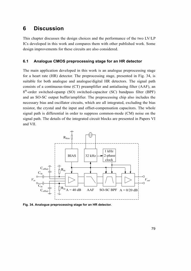
79
6 Discussion
This chapter discusses the design choices and the performance of the two LV/LP
ICs developed in this work and compares them with other published work. Some
design improvements for these circuits are also considered.
6.1 Analogue CMOS preprocessing stage for an HR detector
The main application developed in this work is an analogue preprocessing stage
for a heart rate (HR) detector. The preprocessing stage, presented in Fig. 34, is
suitable for both analogue and analogue/digital HR detectors. The signal path
consists of a continuous-time (CT) preamplifier and antialiasing filter (AAF), an
8th-order switched-opamp (SO) switched-capacitor (SC) bandpass filter (BPF)
and an SO-SC output buffer/amplifier. The preprocessing chip also includes the
necessary bias and oscillator circuits, which are all integrated, excluding the bias
resistor, the crystal and the input and offset-compensation capacitors. The whole
signal path is differential in order to suppress common-mode (CM) noise on the
signal path. The details of the integrated circuit blocks are presented in Papers VI
and VII.
Fig. 34. Analogue preprocessing stage for an HR detector.
BIAS 32 kHz
A = 40 dB AAF SO-SC BPF
Vin Vout
A = 0/20 dB
1 kHz 2-phase clock
Rbias
Cin
Cin
Coffset
Coffset
Rin
Rin
80
6.1.1 Design choices
Specifications for the analogue LV/LP preprocessing stage for a heart rate HR
detector were developed from data obtained from field tests in which signals were
recorded for people during exercise1. The field tests suggested the use of an 8th-
order BPF with corner frequencies of 8 and 30 Hz and a minimum signal-to-
noise-ratio (SNR) of 20 dB for reliable HR detection. Since the signal level of the
ECG obtained from the chest electrodes can typically vary between 100 μV and 2
mV (peak-to-peak), the input stage of the QRS detector has to be designed for
low noise operation. Furthermore, the DC offset voltage of up to 300 mV, caused
by the ECG electrodes, has to be cancelled. Other specifications for the sub-
circuits for the preprocessing stage also depend on circuit level design choices,
which are explained in the following paragraphs.
The 8th-order BPF is realized with SC technique. The choice has been mainly
affected by the need for a fairly accurate frequency response in order to maximize
the SNR of the QRS complexes to be detected in the presence of noise, e.g.
during sport exercise. The accuracy of SC filter coefficients relies on the accuracy
of capacitor ratios and the clock frequency. Because the capacitor ratios can be
made very accurate (in the order of 0.1%), a crystal oscillator has been chosen for
this application to ensure the overall accuracy of the filter. LV operation is
achieved by using an SO-SC structure for the QRS filter. Power consumption of
the filter is optimized by using a ladder filter topology, which offers a much
smaller spread of capacitance values and therefore also a smaller total amount of
capacitors than, for example, a biquad topology in this specific application. In
addition the SOs are optimized for LP operation by using an existing mirror OTA
topology. The open-loop gain of the current mirror OTA is lower than the gain of
a 2-stage OPA, but it consumes less power since it is compensated by the load
capacitance, unlike an OPA which needs an additional compensation capacitor
between the input and output stages. Because the filter topology does not include
any high-quality factor (high-Q) poles, the gain of an OTA structure is adequate
for the desired purpose.
The drawback of choosing a ladder filter topology instead of a biquad
topology is that the input signal can not be directly coupled through a capacitor.
Therefore, a series switch exists on the signal path. The series switch has to
__________________________ 1This aspect is beyond the scope of the thesis and will not be discussed in more detail in this context.

81
conduct the whole signal swing of the preceding CT stage, which in this case is
the preamplifier with an embedded AAF. Because it turned out to be difficult to
design a fully-differential (FD), low-noise opamp with a rail-to-rail output
capability for the preamplifier, the preamplifier was implemented with two
parallel single-ended (SE) opamps with an input/output CM voltage closer to the
negative supply rail, i.e. ground. This also relieves the requirements for the
switches allowing NMOS transistors to be used as sampling switches at the
output of the preamplifier.
The preamplifier consists of two single-ended, 2-stage differential difference
amplifier (DDA) [164] structures. The other input of the DDA is used for
amplifying the weak ECG signal and the other input is used for the amplifier’s
offset compensation. The signal is AC coupled with an external capacitor and an
internal n-well resistor to cancel the electrode offset at the input of the amplifier.
By using two SE amplifiers in parallel instead of one FD, the need of an LV rail-
to-rail common-mode feedback (CMFB) circuit can be avoided, which results in
simpler realization and lower power consumption. The drawback is that a CM
signal (noise) is not attenuated until in the SO-SC filter. Therefore, the
amplification is internally limited to 40 dB which results in a ±100 mV maximum
output voltage with the specified maximum signal level of ±1 mV at the input of
the preamplifier, thus leaving some safety margin for the CM variations. The
amplification is set by using a non-inverting topology with large n-well resistors.
The reference voltage, i.e. the analogue ground voltage for the preamplifier, is
generated by the bias circuit and set with an internal analogue ground buffer to
approximately 0.4 V. The preamplifier has been designed for low noise operation
to provide adequate SNR with the lowest specified input voltage level of 100 μVp-
p. The amplifier’s offset compensation is realized with on-chip transconductance
elements and off-chip capacitors. The pole of the embedded AAF is set by the
bias current and the Miller-compensation capacitor of the preamplifier.
The last stage on the signal path is an SO-SC output buffer/amplifier which
can be used for driving the next signal processing stage on-chip or, as in this case,
an external printed circuit board (PCB) load of the measurement setup.
6.1.2 Performance
Paper VII presents complete measurement results for the fabricated 1-V analogue
CMOS front-end for an HR detector. Since the presented chip, as far as this
author’s knowledge extends, is the first published very low-voltage preprocessing
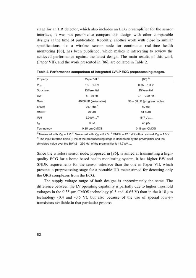
82
stage for an HR detector, which also includes an ECG preamplifier for the sensor
interface, it was not possible to compare this design with other comparable
designs at the time of publication. Recently, another work with close to similar
specifications, i.e. a wireless sensor node for continuous real-time health
monitoring [86], has been published, which makes it interesting to review the
achieved performance against the latest design. The main results of this work
(Paper VII), and the work presented in [86], are collated in Table 2.
Table 2. Performance comparison of integrated LV/LP ECG preprocessing stages.
Property Paper VII 1) [86] 2)
VDD 1.0 – 1.8 V 0.65 – 1.8 V
Structure Differential Differential
BW 8 – 30 Hz 0.1 – 300 Hz
Gain 40/60 dB (selectable) 38 – 58 dB (programmable)
SNDR 36.1 dB 3) 60 dB
CMRR 82 dB 61.9 dB
IRN 5.0 μVrms4) 18.7 μVrms
Itot 3 µA 45 µA
Technology 0.35 μm CMOS 0.18 μm CMOS
1) Measured with VDD = 1 V. 2) Measured with VDD = 0.7 V. 3) SNDR = 42.0 dB with a nominal VDD = 1.5 V. 4) The input referred noise (IRN) of the preprocessing stage is dominated by the preamplifier and the
simulated value over the BW (2 – 250 Hz) of the preamplifier is 14.7 µVrms.
Since the wireless sensor node, proposed in [86], is aimed at transmitting a high-
quality ECG for a home-based health monitoring system, it has higher BW and
SNDR requirements for the sensor interface than the one in Paper VII, which
presents a preprocessing stage for a portable HR meter aimed for detecting only
the QRS complexes from the ECG.
The supply voltage range of both designs is approximately the same. The
difference between the LV operating capability is partially due to higher threshold
voltages in the 0.35 µm CMOS technology (0.5 and -0.65 V) than in the 0.18 µm
technology (0.4 and -0.6 V), but also because of the use of special low-VT
transistors available in that particular process.
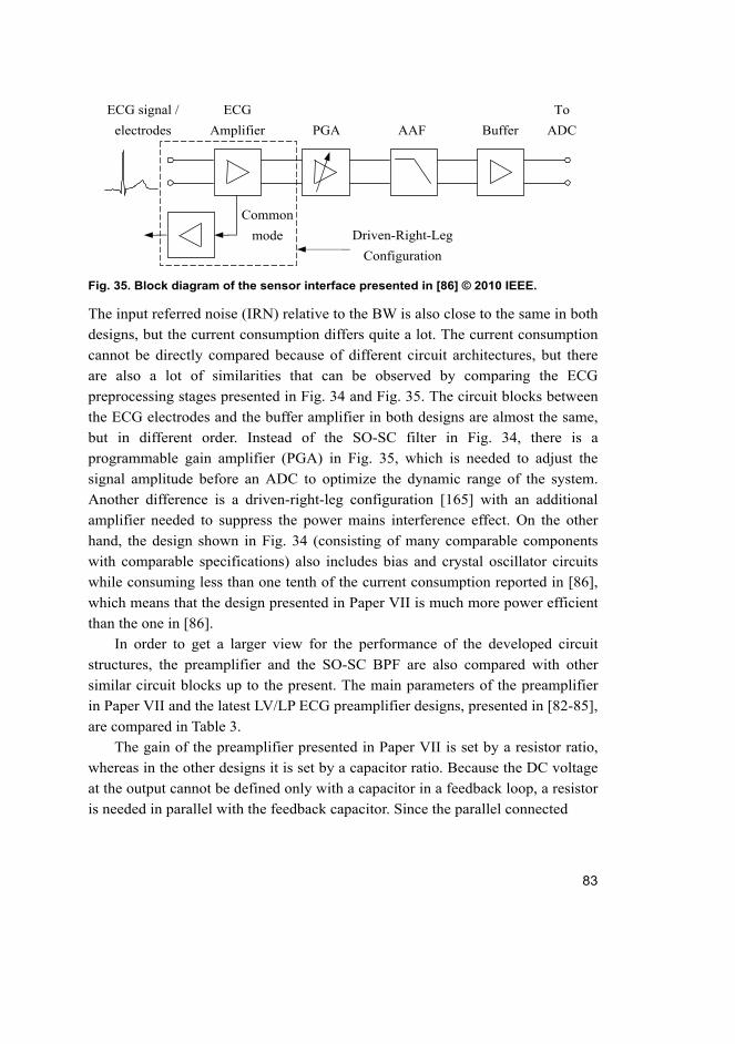
83
Fig. 35. Block diagram of the sensor interface presented in [86] © 2010 IEEE.
The input referred noise (IRN) relative to the BW is also close to the same in both
designs, but the current consumption differs quite a lot. The current consumption
cannot be directly compared because of different circuit architectures, but there
are also a lot of similarities that can be observed by comparing the ECG
preprocessing stages presented in Fig. 34 and Fig. 35. The circuit blocks between
the ECG electrodes and the buffer amplifier in both designs are almost the same,
but in different order. Instead of the SO-SC filter in Fig. 34, there is a
programmable gain amplifier (PGA) in Fig. 35, which is needed to adjust the
signal amplitude before an ADC to optimize the dynamic range of the system.
Another difference is a driven-right-leg configuration [165] with an additional
amplifier needed to suppress the power mains interference effect. On the other
hand, the design shown in Fig. 34 (consisting of many comparable components
with comparable specifications) also includes bias and crystal oscillator circuits
while consuming less than one tenth of the current consumption reported in [86],
which means that the design presented in Paper VII is much more power efficient
than the one in [86].
In order to get a larger view for the performance of the developed circuit
structures, the preamplifier and the SO-SC BPF are also compared with other
similar circuit blocks up to the present. The main parameters of the preamplifier
in Paper VII and the latest LV/LP ECG preamplifier designs, presented in [82-85],
are compared in Table 3.
The gain of the preamplifier presented in Paper VII is set by a resistor ratio,
whereas in the other designs it is set by a capacitor ratio. Because the DC voltage
at the output cannot be defined only with a capacitor in a feedback loop, a resistor
is needed in parallel with the feedback capacitor. Since the parallel connected
ECG
Amplifier
PGA
To
ADC
ECG signal /
electrodes
Buffer
AAF
Driven-Right-Leg
Configuration
Common
mode
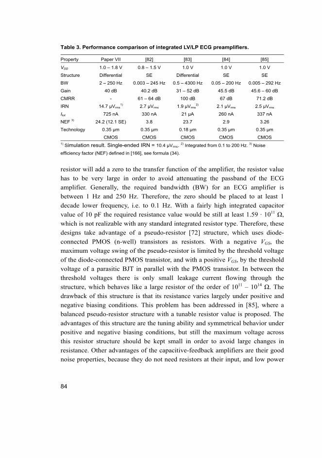
84
Table 3. Performance comparison of integrated LV/LP ECG preamplifiers.
Property Paper VII [82] [83] [84] [85]
VDD 1.0 – 1.8 V 0.8 – 1.5 V 1.0 V 1.0 V 1.0 V
Structure Differential SE Differential SE SE
BW 2 – 250 Hz 0.003 – 245 Hz 0.5 – 4300 Hz 0.05 – 200 Hz 0.005 – 292 Hz
Gain 40 dB 40.2 dB 31 – 52 dB 45.5 dB 45.6 – 60 dB
CMRR - 61 – 64 dB 100 dB 67 dB 71.2 dB
IRN 14.7 μVrms1) 2.7 μVrms 1.9 μVrms
2) 2.1 μVrms 2.5 μVrms
Itot 725 nA 330 nA 21 μA 260 nA 337 nA
NEF 3) 24.2 (12.1 SE) 3.8 23.7 2.9 3.26
Technology 0.35 μm
CMOS
0.35 μm
CMOS
0.18 μm
CMOS
0.35 μm
CMOS
0.35 μm
CMOS 1) Simulation result. Single-ended IRN = 10.4 μVrms.
2) Integrated from 0.1 to 200 Hz. 3) Noise
efficiency factor (NEF) defined in [166], see formula (34).
resistor will add a zero to the transfer function of the amplifier, the resistor value
has to be very large in order to avoid attenuating the passband of the ECG
amplifier. Generally, the required bandwidth (BW) for an ECG amplifier is
between 1 Hz and 250 Hz. Therefore, the zero should be placed to at least 1
decade lower frequency, i.e. to 0.1 Hz. With a fairly high integrated capacitor
value of 10 pF the required resistance value would be still at least 1.59 · 1011 Ω,
which is not realizable with any standard integrated resistor type. Therefore, these
designs take advantage of a pseudo-resistor [72] structure, which uses diode-
connected PMOS (n-well) transistors as resistors. With a negative VGS, the
maximum voltage swing of the pseudo-resistor is limited by the threshold voltage
of the diode-connected PMOS transistor, and with a positive VGS, by the threshold
voltage of a parasitic BJT in parallel with the PMOS transistor. In between the
threshold voltages there is only small leakage current flowing through the
structure, which behaves like a large resistor of the order of 1011 – 1014 Ω. The
drawback of this structure is that its resistance varies largely under positive and
negative biasing conditions. This problem has been addressed in [85], where a
balanced pseudo-resistor structure with a tunable resistor value is proposed. The
advantages of this structure are the tuning ability and symmetrical behavior under
positive and negative biasing conditions, but still the maximum voltage across
this resistor structure should be kept small in order to avoid large changes in
resistance. Other advantages of the capacitive-feedback amplifiers are their good
noise properties, because they do not need resistors at their input, and low power
85
consumption, because the only resistive load they have to drive is the pseudo-
resistor in the feedback loop of the amplifier.
All of the presented preamplifiers are capable of operating with a 1.0-V
supply voltage. In Paper VII and [83] the signal path is differential, whereas in
[82, 84, 85] it is single-ended. Because the preamplifier in Paper VII consists of
two identical SE amplifiers, its current consumption can be halved when
compared with the SE topologies. Therefore, no significant difference exists
between the current consumption of this and the other design. However, the
current consumption of the differential preamplifier presented in [83] is much
higher than that in other designs, but its tunable frequency range is also larger,
which partially explains the difference.
The common-mode rejection ratio (CMRR) of the differential topology [83]
is also higher than that in the other designs. The CMRR of the preamplifier in
Paper VII is not mentioned because the CM signals are rejected at the next stage,
which is a fully-differential SO-SC filter. The CMRR measured at the output of
the SO-SC filter is approximately 82 dB.
Since there are no output pins between the preamplifier and the SO-SC filter
presented in Paper VII, the noise contribution of the preamplifier could not be
directly measured from its output. Despite that it can be estimated from the
simulated input referred noise (IRN) by integrating the 1/f noise and the white
noise over the BW of the preamplifier and quadratically summing them together.
The 1/f noise is dominated by the input transistors, as defined in (1), whereas the
white noise depends both on the input stage’s transistors, as stated in (2), and the
noise generated by the two input resistors Rin (shown in Fig. 34) of the
preamplifier. The effective noise bandwidth of the preamplifier is the bandwidth
of a brick-wall filter, which has the same amplification and area as the frequency
response of the preamplifier.
Since the measured SNR at the output of the whole ECG preprocessing chip
over the SC filter’s BW from 8 to 30 Hz with the minimum specified input signal
level of 100 μV(p-p) (= 35.3 μVrms) was 17 dB, the rms noise at the output of the
chip can be calculated from
rmsrmsinrmsout
outtotn VSNR
GainV
SNR
VV μ499)()(
),( =⋅
== (33)
which, when divided by the gain of the preamplifier, gives 4.99 µVrms as the total
IRN from 8 to 30 Hz. The simulated value for the same BW is 5.29 µVrms, which
is in good agreement with the measured value and proves that the noise of the
86
overall system is dominated by the preamplifier. The simulated noise of the
preamplifier over its own BW from 2 to 250 Hz is 14.7 µVrms, which is used for
calculating the noise efficiency factor (NEF) of the preamplifier.
The NEF, introduced in [166], describes how many times the noise of a
system with the same current consumption and bandwidth is higher when
compared to the ideal case, which is an ideal BJT with only thermal noise. The
NEF is calculated from
( , )
24.22
12.1 ( )4tot
n tot inT
INEF V
SEU kT BWπ
= = ⋅ ⋅ ⋅ (34)
where Itot is the total current consumption, UT = kT/q is the thermal voltage (~26
mV at room temperature), k is the Boltzmann's constant, T is the temperature, q is
the electron’s charge and BW the bandwidth of the preamplifier. The NEF is
calculated for both differential and SE cases to make the comparison easier. The
NEF of the differential preamplifier is comparable to the other differential
topology presented in Table 3, and the NEF of an SE version would be about four
times larger than the NEF of the best SE capacitive-feedback amplifiers. The
main reason for the higher NEF in this design is the DDA amplifier structure,
which has two identical input stages (one for the offset compensation and one for
the signal path), thus doubling the IRN and NEF figures.
In order to get a larger view for the current consumption and the noise
efficiency figures of biosignal preamplifiers, the current consumption and NEF of
this and other published works (also with higher supply voltages) are compared in
Fig. 36. The amplifiers presented in [20, 59, 68, 73, 74, 77, 78, 81-85, 166, 167]
and Paper VII are designed for ECG measurements or more versatile biosignal
measurements, also including electroencephalography (EEG), electromyography
(EMG) or electro-oculography (EOG) measurement abilities, whereas the designs
in [72, 75, 79, 168-173] are purely aimed for neural (EEG) recordings. The
preamplifiers presented in [20, 68, 169] and Paper VII are continuous-time
voltage amplifiers based on a resistor ratio and the ones in [59, 72, 78, 82-85, 170,
171, 173] are based on a capacitor ratio. The preamplifiers presented in [73, 166-
168] are based on active current feedback topologies and the front-stage presented
in [172] is based on an auto-zeroing DDA-topology. As expected, the capacitive-
feedback amplifiers generally achieve lower NEF than the resistive-feedback
amplifiers. Chopper-stabilized topologies [74, 75, 77, 79, 81] are also very good
choices for low-noise amplifiers due to their inherently good 1/f noise properties,

87
Fig. 36. Current consumption vs. normalized noise of the preamplifier presented in
Paper VII and the amplifiers presented in other publications. Resistive feedback
topologies are marked with triangles, capacitive feedback topologies with circles,
chopper-stabilized topologies with crosses, active current feedback topologies with
plusses and others with squares. Dashed lines indicate constant NEF contours.
but their current consumption is higher because of more complex circuit
structures.
The preamplifier presented in Paper VII features one of the best NEFs
amongst the resistive feedback topologies, right after the SE topology presented
in [20]. As a single-ended version, the current consumption is the lowest of all
resistive feedback topologies (all the other resistive feedback amplifiers in Fig. 36
are SE versions) being close to the lowest realized with capacitive feedback
topologies. When taking the supply voltage into account, Paper VII has the lowest
power consumption of all resistive feedback amplifiers being 725 nW from a 1-V
supply as a differential version and 363 nW as an SE version while, for example,
the preamplifier presented in [68] consumes 900 nW from a 2-V supply as an SE
version.
The other part of the preprocessing stage presented in Paper VII is an SO-SC
BPF for HR detection. The BPF is needed in order to maximize the SNR of QRS
complexes in a cardiac signal before further processing. Since the largest noise
[68]
[75]
[79]
[83]
[169]
[172]
[81] [20]
[72]
[73]
[74]
[77]
[78]
[82][84]
[85]
Paper VII
Paper VII (SE)[168]
[170]
[171]
[173]
[166]
[59]
[167]
1,00E-07
1,00E-06
1,00E-05
1,00E-04
1,00E-03
1,00E-08 1,00E-07 1,00E-06 1,00E-05
Input referred noise [Vrms/(Hz)1/2]
Cu
rre
nt
con
sum
ptio
n [
A]
NEF = 1
NEF = 10 NEF = 100
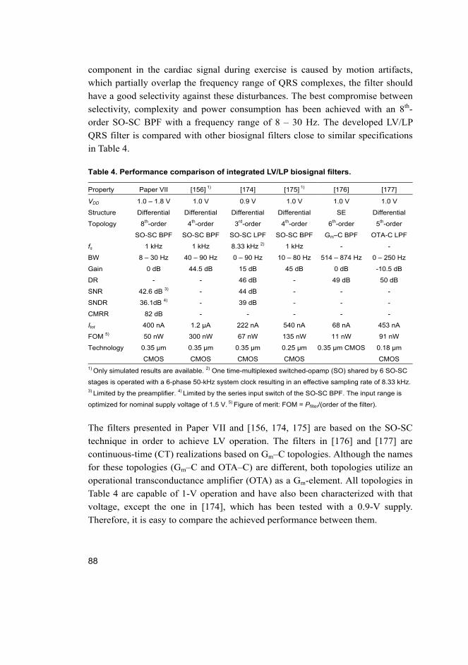
88
component in the cardiac signal during exercise is caused by motion artifacts,
which partially overlap the frequency range of QRS complexes, the filter should
have a good selectivity against these disturbances. The best compromise between
selectivity, complexity and power consumption has been achieved with an 8th-
order SO-SC BPF with a frequency range of 8 – 30 Hz. The developed LV/LP
QRS filter is compared with other biosignal filters close to similar specifications
in Table 4.
Table 4. Performance comparison of integrated LV/LP biosignal filters.
Property Paper VII [156] 1) [174] [175] 1) [176] [177]
VDD 1.0 – 1.8 V 1.0 V 0.9 V 1.0 V 1.0 V 1.0 V
Structure Differential Differential Differential Differential SE Differential
Topology 8th-order
SO-SC BPF
4th-order
SO-SC BPF
3rd-order
SO-SC LPF
4th-order
SO-SC BPF
6th-order
Gm–C BPF
5th-order
OTA-C LPF
fs 1 kHz 1 kHz 8.33 kHz 2) 1 kHz - -
BW 8 – 30 Hz 40 – 90 Hz 0 – 90 Hz 10 – 80 Hz 514 – 874 Hz 0 – 250 Hz
Gain 0 dB 44.5 dB 15 dB 45 dB 0 dB -10.5 dB
DR - - 46 dB - 49 dB 50 dB
SNR 42.6 dB 3) - 44 dB - - -
SNDR 36.1dB 4) - 39 dB - - -
CMRR 82 dB - - - - -
Itot 400 nA 1.2 μA 222 nA 540 nA 68 nA 453 nA
FOM 5) 50 nW 300 nW 67 nW 135 nW 11 nW 91 nW
Technology 0.35 μm
CMOS
0.35 μm
CMOS
0.35 μm
CMOS
0.25 μm
CMOS
0.35 μm CMOS 0.18 μm
CMOS 1) Only simulated results are available. 2) One time-multiplexed switched-opamp (SO) shared by 6 SO-SC
stages is operated with a 6-phase 50-kHz system clock resulting in an effective sampling rate of 8.33 kHz. 3) Limited by the preamplifier. 4) Limited by the series input switch of the SO-SC BPF. The input range is
optimized for nominal supply voltage of 1.5 V. 5) Figure of merit: FOM = Pfilter/(order of the filter).
The filters presented in Paper VII and [156, 174, 175] are based on the SO-SC
technique in order to achieve LV operation. The filters in [176] and [177] are
continuous-time (CT) realizations based on Gm–C topologies. Although the names
for these topologies (Gm–C and OTA–C) are different, both topologies utilize an
operational transconductance amplifier (OTA) as a Gm-element. All topologies in
Table 4 are capable of 1-V operation and have also been characterized with that
voltage, except the one in [174], which has been tested with a 0.9-V supply.
Therefore, it is easy to compare the achieved performance between them.
89
Since the most important parameters for the designed QRS filter are LV/LP
operation and steepness of the stop-band attenuation, a suitable figure of merit
(FOM) for this design is the power consumption divided by the filter order, used
in [174]. The QRS filter presented in Paper VII has the lowest FOM of 50
nW/pole from all SO-SC topologies. This is due to a very power efficient SO
structure, which is based on a fully-differential current mirror OTA amplifier with
a CMFB circuit. Although the frequency bands of the SO-SC filters presented in
Table 4 are slightly different, the requirements for the opamps are mainly set by
the sampling frequency (assuming low-Q filter poles), which is 1 kHz in Paper
VII and references [156] and [175]. Therefore, the power efficiency of these
filters can be directly compared by dividing the power consumption by the filter
order, which is at the same time the amount of SOs included in the filter.
The filter presented in [174] is quite different from the other three SO-SC
designs because it uses only one time-multiplexed SO which is shared by six
consecutive stages (three for the 3rd-order low-pass filter and three for a 3rd-order
ΣΔ modulator). For this reason, the internal amplifier structure consists of two
parallel output stages which are active during both clock phases. Furthermore,
this opamp is used in six consecutive stages, which is accomplished by time-
sharing. The time-sharing causes the effective sampling rate of one filter stage to
be one sixth of the original system clock frequency, which is 50 kHz divided by 6,
i.e. 8.33 kHz. On the other hand, the power consumption increases because the
opamp has to be designed to meet the settling requirements with 50 kHz clock
frequency, but then again the amount of opamps is reduced to only one, which
decreases the power consumption. The net effect in this case is that the power
consumption per filter pole in [174] is higher than in Paper VII. When taking the
sampling frequency into consideration, the design presented in [174] would be
more power efficient if its effective sampling frequency were lowered to 1 kHz.
This is due to a lower bias current needed for the opamp to maintain the same
settling performance than with the original operating frequency.
The most power efficient design in Table 4 is the single-ended Gm–C filter
presented in [176]. It consists of eight Gm-elements and six capacitors realizing a
6th-order ladder filter topology. The filter is originally designed as a part of a
breathing detector, but its programmable frequency range extends from a center
frequency of 100 Hz to approximately 20 kHz, thus making it suitable also for
many other biomedical applications. The performance figures listed in Table 4 are
the measurement results obtained for the nominal center frequency of 670 Hz.
Since the center frequency is linearly programmable with a bias current, the
90
estimated current consumption at 100 Hz is approximately only 10 nA, which
makes it an interesting alternative for the QRS filter described in Paper VII. The
linear input voltage range in [176] is 40 mVp-p, which is smaller than the 200
mVp-p input voltage range of the SO-SC filter presented in Paper VII.
Another LV/LP Gm–C filter, proposed in [177], is aimed at ECG filtering with
a bandwidth of 250 Hz. This filter consists of eleven Gm-elements and five
capacitors realizing a 5th-order low-pass ladder filter topology. This design makes
use of a more complex Gm-element than the one in [176], resulting in a larger
input voltage range of 200 mVp-p (although the measurements have been carried
out with a 100-mVp-p input level) but with the expense of increased current
consumption, which is even larger than the current consumption for the SO-SC
BPF in Paper VII. Furthermore, this design attenuates the passband by 10.5 dB,
which is explained partially by the topology and partially by the finite output
resistance of the OTAs.
Since the accuracy requirements for the QRS filter parameters are quite strict,
the filter has to be very robust against process, temperature, supply voltage and
component variations. The accuracy of SC filters is mainly dependent on the
accuracy of on-chip capacitor ratios and sampling frequency, assuming that the
opamps used in the SC-integrators exceed their minimum specified performance
requirements in all conditions. Since the accuracy of the capacitor ratios can reach
0.1% with a careful layout design, the total accuracy with a crystal oscillator-
based system can easily be within 1%. The situation with Gm–C filters is quite
different since the accuracy of their filter coefficients depends on two dissimilar
elements, namely the transconductor and the capacitor, which do not track each
other. Therefore, both the Gm-elements and the capacitors have to be well
matched altogether. Furthermore, the requirements for the Gm-elements are much
more stringent than for the opamps in SC-filters because they have to maintain a
constant transconductance over the passband with all signal levels. Since the
linear input voltage range (within 1%) of a conventional transconductor based on
an OTA can reach only a few tens of millivolts, a large number of different
variations for Gm-elements and their linearization techniques have been proposed
in the literature. Although the transconductance values for the Gm-elements can be
made linear and quite well-matched with each other in a limited input voltage
range, they still need to be compensated against the temperature and the supply
voltage variations. For this reason, the Gm–C filters also need some sort of a
tuning circuit that locks their transconductance values to an appropriate stable
reference, which is usually a clock signal generated by an internal or an external
91
oscillator. The Gm–C filter presented in [176] is externally tunable with a bias
current, while the one in [177] uses external voltage. Neither of them includes an
on-chip tuning circuit, whereas the design presented in Paper VII includes all the
necessary peripheral circuit blocks, including a bias circuit and a crystal oscillator.
On top of the presented design challenges, the additional tuning circuit (which
also needs to be accurate) needed by the Gm–C filter topologies in [176] and [177]
would also increase their total power consumption and area, a factor which
decreases their attractiveness in this particular application.
6.1.3 Future work
Even though the designed QRS detector chip fulfills the performance
requirements set by the application, there are a couple of issues that need to be
considered when improving the design. The first of them is related to the
preamplifier of the QRS detector. In the present design, two single-ended
amplifiers, instead of one differential one, are used in parallel to make differential
signal processing possible in the subsequent stages. The drawback of this choice
is that common-mode (CM) disturbances, like motion artifacts and noise, are
passing through until the first genuinely differential stage, namely the SC filter. A
large unwanted CM component in the signal path might then saturate the output
of the preamplifier (because of the large amplification of the order of 40 dB
needed) resulting in missed beats at the output of the whole QRS detector. In the
case of a fully-differential amplifier, this would not be a problem since the
common-mode feedback (CMFB) circuit will remove the CM component at the
output as long as the input stage of the preamplifier is not saturated. The problem
is to find a CMFB circuit for the preamplifier which would operate reliably from
rail to rail with all specified supply voltages and a low current consumption. The
answer to this problem may well be found in floating-gate or bulk-driven
techniques, as discussed in Chapter 4.
Another way to improve the performance of the preamplifier is to use a
capacitive feedback instead of a resistive feedback for the preamplifier, which
enables better noise performance with probably lower power consumption.
Otherwise, the main problem is the same, i.e. how to implement a fully-
differential structure in an LV environment.
If a suitable fully-differential structure with a rail-to-rail output capability
was to be developed then the next improvement for the performance would be
achieved by using a rail-to-rail series switch (a bootstrapped switch [145-150] or
92
a switch built with amplifiers [158, 159]) in between the continuous-time (CT)
preamplifier and the following switched-opamp switched-capacitor (SO-SC) filter,
or to change the SC filter topology to another type of topology (like the bandpass
biquad filters presented in [153, 156]) that do not require a series switch. The
choice of the filter topology might impact strongly on the total amount of filter
capacitances, as described in Chapter 6.1.1, something which inevitably increases
the current consumption.
Since the preprocessing stage for a QRS detector is most probably going to
be integrated as a part of a more complex system, such as a heart rate detector
chip with an integrated decision algorithm and parameter calculations, it is worth
considering at which point it would be wise to convert the ECG signal into digital
form. The first point could be right after the CT preamplifier and another point
would be after the SO-SC filter and the third choice is to combine the SC-filter
and the ADC, as in [174]. Because the developed LV/LP circuits and structures
can be exploited, for example in the design of LV/LP ΣΔ modulators, the next step
would be to study different LV/LP A/D converter topologies for optimal circuit
level realization of the whole system.
6.2 RC oscillator for clock and sensor applications
A functional circuit block diagram and a timing diagram of the developed RC
oscillator are presented in Fig. 37. The integrated circuit comprises of a charge
pump (CP) driven, voltage-controlled oscillator (VCO), a frequency divider (1/N),
a comparator (COMP), a logic circuit (LOGIC) and a few switches. The only
external components of the oscillator are passive components R and C. Detailed
circuit description of the RC oscillator is given in Papers IV and VIII.
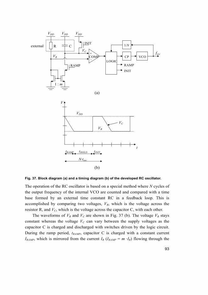
93
Fig. 37. Block diagram (a) and a timing diagram (b) of the developed RC oscillator.
The operation of the RC oscillator is based on a special method where N cycles of
the output frequency of the internal VCO are counted and compared with a time
base formed by an external time constant RC in a feedback loop. This is
accomplished by comparing two voltages, VR, which is the voltage across the
resistor R, and VC, which is the voltage across the capacitor C, with each other.
The waveforms of VR and VC are shown in Fig. 37 (b). The voltage VR stays
constant whereas the voltage VC can vary between the supply voltages as the
capacitor C is charged and discharged with switches driven by the logic circuit.
During the ramp period, tRAMP, capacitor C is charged with a constant current
IRAMP, which is mirrored from the current IR (IRAMP = m ·IR) flowing through the
R C
1 : m
LOGIC RAMP
INIT
INIT
RAMP
COMP _ +
CP VCO
1/N
fosc VR
VC
VDD VDD VDD
external
V
VR
VDD
VC
t tRAMP tHOLD tINIT
N·tosc
(a)
(b)
94
resistor R. During the hold period, the switches are open and VR is compared with
VC by the comparator. If VC is higher than VR, i.e. the period of the VCO is shorter
than desired, the logic circuit drives the charge pump to update the input voltage
of the VCO in order to increase its period. If VC is lower than VR, the VCO is
updated to decrease its period. When VC is equal to VR, the frequency of the VCO
has reached the desired value and is no longer adjusted, as long as the equilibrium
is maintained. During initializing period tINIT, the capacitor C is discharged. It
should be noted that there are no additional delays present in this topology, since
the output of the comparator is read at the end of the hold period, which is long
enough for proper settling of the comparator.
The operation of the RC oscillator can also be explained by the following
relationships:
R
VmI R
RAMP ⋅= (35)
oscRAMP tN
t ⋅=4
(36)
RAMPRAMPR tICV ⋅= (37)
RC
mN
tf
oscosc 4
1 == (38)
where
IRAMP ramp current, tRAMP time of charging C, VR voltage across resistor R, tosc period of the oscillator, fosc frequency of the oscillator, m current ratio IRAMP/IR, N division ratio of the frequency divider, R external resistance to set the frequency, C external capacitance to set the frequency.
The last relationship (38) shows that the output frequency of the oscillator is also
independent of supply voltage, temperature and process variations. As N can be
assumed ideal, the accuracy of the oscillator mainly depends on the accuracy of
the current mirror ratio m and the external time constant RC. Since the accuracy
of m can be within 1% with careful layout design, the total accuracy of the RC
oscillator mainly depends on the accuracy of external passive components R and
95
C and their parasitic components caused by the inside/outside (I/O) interface of
the chip. Therefore, sufficiently high values for R and C are used to suppress the
effect of additional parasitic components.
6.2.1 Design choices
The chosen topology (Fig. 37) can be optimized for many applications by
choosing the values for the desired operating frequency and passive components
R and C. In this work, the primary goal has been to achieve an accurate and stable
5-MHz clock oscillator with a reasonable settling time of < 1 s without tuning and
to minimize the power consumption. The best compromise between these
requirements was achieved with the following combination of design parameters
(see formula (38)):
m = 3.91 N = 512 R = 100 kΩ C = 1 nF
Another goal of this work has been to increase the versatility of the used topology
to be also used in resistive and capacitive sensor applications.
The developed RC oscillator (Fig. 37) is powered by a very simple bias
structure consisting of an external resistor and a diode-connected transistor. The
reason for this is the requirement for a very low supply voltage of 1 – 1.5 V. The
drawback of this structure is that the bias current levels of the whole chip are
increasing with the supply voltage. On the other hand, this is not a problem since
the aimed supply voltage range is only a few hundred mV, which corresponds to
the life-time of a single battery cell. In the first version (Paper IV), the diode
connected bias transistor and the following current mirrors are realized with
single transistors, which allows the use of a supply voltage as low as 1 V in a
process technology with threshold voltages of VTN = 0.5 V and VTP = -0.65 V.
Since the frequency accuracy of the first version was dominated by the accuracy
of the current mirrors, another version (Paper VIII) with LV cascode current
mirrors was designed. This change increases the minimum supply voltage
requirement by approximately 0.2 V, but leads to more accurate overall
performance.
96
The VCO is realized with a current-starved 5-stage ring oscillator, which
satisfies the LV/LP and operating frequency range requirements set for this work.
The operating frequency is controlled with a charge pump (CP) structure [178],
which also minimizes the parasitic injection from the switches to the integrating
capacitor. The opamp needed by the structure is realized with a two-stage Miller-
compensated opamp with a bulk-driven (BD) input stage (presented in Fig. 23).
The BD-opamp enables the CP to set the control voltage of the VCO precisely to
any value between the supply voltages. The CP current in the first design (Paper
IV) is mirrored directly from the bias current, which causes the update step size of
the CP to be supply voltage dependent. In the second design (Paper VIII), the CP
current is realized with a dynamic current generator (DCG), which generates the
CP current based on the voltage difference VR – VC (see Fig. 37) across external
components R and C. When VR – VC is large (i.e. the operating frequency is far
from the desired) the update step is large and when VR – VC is small the update
step is small, which leads to both faster settling and smaller jitter of the oscillator.
The input stage of the DCG is of BD type to allow rail-to-rail input signals.
The digital part of the chip in both designs, presented in Papers IV and VIII,
is designed with full-custom components, because the standard library cells,
which are optimized for 3.3 V supply voltage, do not operate satisfactorily (or not
at all) with supply voltages down to 1 V.
6.2.2 Performance
A summary of the measurement results of the developed self-calibrating RC
oscillator, described in Paper VIII, and the performance of other published LV/LP
designs are collated in Table 5. All the other designs are true LV designs, except
[97, 98], which are taken into comparison due to their good frequency stability for
being fully integrated RC oscillators. Other fully integrated RC oscillators are [94]
and [103], which means they can be used only as clock generators and not as
sensor interfaces. The only RC oscillators which can be used for both applications
are the ones presented in Paper VII and [105]. These designs are based on the
same operation principle but the one in [105] includes an additional programming
on-the-fly option.
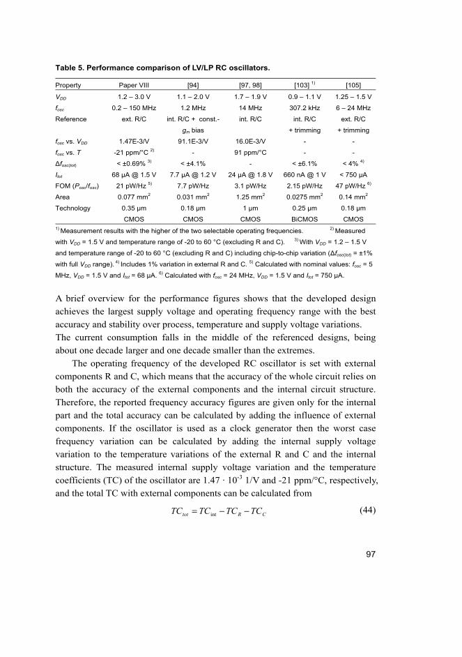
97
Table 5. Performance comparison of LV/LP RC oscillators.
Property Paper VIII [94] [97, 98] [103] 1) [105]
VDD 1.2 – 3.0 V 1.1 – 2.0 V 1.7 – 1.9 V 0.9 – 1.1 V 1.25 – 1.5 V
fosc 0.2 – 150 MHz 1.2 MHz 14 MHz 307.2 kHz 6 – 24 MHz
Reference ext. R/C int. R/C + const.-
gm bias
int. R/C int. R/C
+ trimming
ext. R/C
+ trimming
fosc vs. VDD 1.47E-3/V 91.1E-3/V 16.0E-3/V - -
fosc vs. T -21 ppm/°C 2) - 91 ppm/°C - -
Δfosc(tot) < ±0.69% 3) < ±4.1% - < ±6.1% < 4% 4)
Itot 68 μA @ 1.5 V 7.7 μA @ 1.2 V 24 μA @ 1.8 V 660 nA @ 1 V < 750 μA
FOM (Posc/fosc) 21 pW/Hz 5) 7.7 pW/Hz 3.1 pW/Hz 2.15 pW/Hz 47 pW/Hz 6)
Area 0.077 mm2 0.031 mm2 1.25 mm2 0.0275 mm2 0.14 mm2
Technology 0.35 μm
CMOS
0.18 μm
CMOS
1 μm
CMOS
0.25 μm
BiCMOS
0.18 μm
CMOS 1) Measurement results with the higher of the two selectable operating frequencies. 2) Measured
with VDD = 1.5 V and temperature range of -20 to 60 °C (excluding R and C). 3) With VDD = 1.2 – 1.5 V
and temperature range of -20 to 60 °C (excluding R and C) including chip-to-chip variation (Δfosc(tot) = ±1%
with full VDD range). 4) Includes 1% variation in external R and C. 5) Calculated with nominal values: fosc = 5
MHz, VDD = 1.5 V and Itot = 68 μA. 6) Calculated with fosc = 24 MHz, VDD = 1.5 V and Itot = 750 μA.
A brief overview for the performance figures shows that the developed design
achieves the largest supply voltage and operating frequency range with the best
accuracy and stability over process, temperature and supply voltage variations.
The current consumption falls in the middle of the referenced designs, being
about one decade larger and one decade smaller than the extremes.
The operating frequency of the developed RC oscillator is set with external
components R and C, which means that the accuracy of the whole circuit relies on
both the accuracy of the external components and the internal circuit structure.
Therefore, the reported frequency accuracy figures are given only for the internal
part and the total accuracy can be calculated by adding the influence of external
components. If the oscillator is used as a clock generator then the worst case
frequency variation can be calculated by adding the internal supply voltage
variation to the temperature variations of the external R and C and the internal
structure. The measured internal supply voltage variation and the temperature
coefficients (TC) of the oscillator are 1.47 · 10-3 1/V and -21 ppm/°C, respectively,
and the total TC with external components can be calculated from
CRtot TCTCTCTC −−= int (44)
98
where the negative signs in front of the temperature coefficients TCR and TCC are
due to the oscillator topology. Since the best thin film resistors can have a
tolerance of 0.1% with a TC of 5 to 25 ppm/°C (foil resistors even ±0.005% and
0.14 ppm/°C) and ceramic capacitors a tolerance of 0.1% with a TC of ±30
ppm/°C, the TCtot of the designed RC oscillator can theoretically reduce to zero
depending on the signs and values of the different TCs. In the measurements, the
TCR was 10 ppm/°C and the TCC was -133 ppm/°C, which resulted in a TCtot of
102 ppm/°C.
The total variation of fosc caused by the internal circuit structure is less than
±0.69% (including chip-to-chip variation), which means that with external
precision components the total accuracy of the oscillator is within ±1%. The
achieved frequency accuracy and stability are clearly the best when compared
with other LV/LP designs in Table 5. Furthermore, it is a self-calibrating structure,
which locks its frequency to the RC time constant and does not need any tuning
or additional references. Therefore, the designed oscillator is very suitable for
both clocking and sensor applications where good accuracy is demanded.
Because of the simple bias current circuit used, the current consumption of
the developed oscillator is strongly dependent on the supply voltage and the
external resistor. With nominal component values (R = 100 kΩ and C = 1 nF @ 5
MHz) the current consumption varies from 48 μA to 68 μA when the supply
voltage is swept from 1.2 to 1.5 V. The current consumption of this design is
larger than that of most of the other designs in Table 5, but it can be dropped
down by increasing R and reducing C and the supply voltage while maintaining
the same operating frequency, if necessary.
Since the main goal of this work was to develop a very low-voltage (≤ 2VT +
Vov) and accurate RC oscillator capable of fairly high operating frequency with
low current consumption, a suitable figure of merit (FOM) for this design is the
power-to-frequency ratio. When compared with other designs, the FOM achieved
by this design seems quite modest but, when taking into account the possibility of
adjusting the component values and the supply voltage, the FOM can be
optimized with respect to the application. For example, if the supply voltage is set
to 1.2 V and the external component values are R = 100 kΩ and C = 100 pF, the
output frequency rises to 50 MHz and the current consumption to 87 μA, resulting
in an FOM of 2.1 pW/Hz, which is already comparable with the best results.
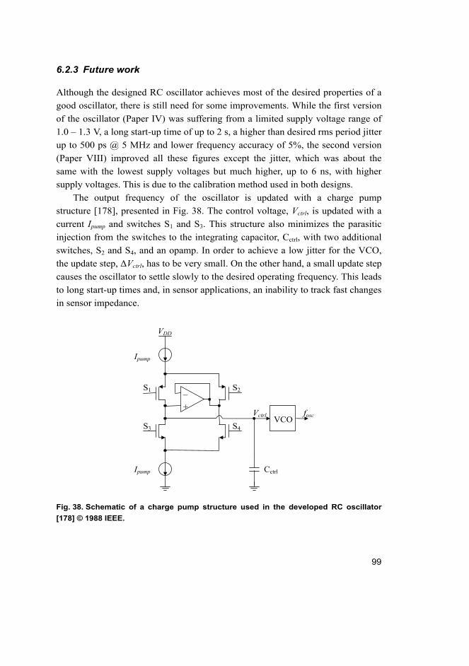
99
6.2.3 Future work
Although the designed RC oscillator achieves most of the desired properties of a
good oscillator, there is still need for some improvements. While the first version
of the oscillator (Paper IV) was suffering from a limited supply voltage range of
1.0 – 1.3 V, a long start-up time of up to 2 s, a higher than desired rms period jitter
up to 500 ps @ 5 MHz and lower frequency accuracy of 5%, the second version
(Paper VIII) improved all these figures except the jitter, which was about the
same with the lowest supply voltages but much higher, up to 6 ns, with higher
supply voltages. This is due to the calibration method used in both designs.
The output frequency of the oscillator is updated with a charge pump
structure [178], presented in Fig. 38. The control voltage, Vctrl, is updated with a
current Ipump and switches S1 and S3. This structure also minimizes the parasitic
injection from the switches to the integrating capacitor, Cctrl, with two additional
switches, S2 and S4, and an opamp. In order to achieve a low jitter for the VCO,
the update step, ΔVctrl, has to be very small. On the other hand, a small update step
causes the oscillator to settle slowly to the desired operating frequency. This leads
to long start-up times and, in sensor applications, an inability to track fast changes
in sensor impedance.
Fig. 38. Schematic of a charge pump structure used in the developed RC oscillator
[178] © 1988 IEEE.
Ipump
Ipump
S1 S2
S3 S4
+
_
VCO
Cctrl
Vctrl fosc
VDD
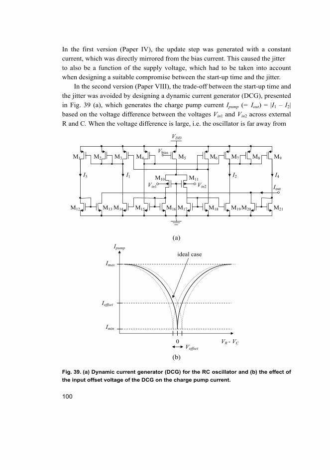
100
In the first version (Paper IV), the update step was generated with a constant
current, which was directly mirrored from the bias current. This caused the jitter
to also be a function of the supply voltage, which had to be taken into account
when designing a suitable compromise between the start-up time and the jitter.
In the second version (Paper VIII), the trade-off between the start-up time and
the jitter was avoided by designing a dynamic current generator (DCG), presented
in Fig. 39 (a), which generates the charge pump current Ipump (= Iout) = |I1 – I2|
based on the voltage difference between the voltages Vin1 and Vin2 across external
R and C. When the voltage difference is large, i.e. the oscillator is far away from
Fig. 39. (a) Dynamic current generator (DCG) for the RC oscillator and (b) the effect of
the input offset voltage of the DCG on the charge pump current.
M12
Vin1 Vin2
M1
VDD
M2 M3 M4 M5 M6 M7 M8 M9
M10 M11
M13 M14 M15 M16 M17 M18 M19 M20 M21
I3 I1 I2 I4
Vbias
Iout
0 VR - VC
Ipump
Imax
Imin
Ioffset
Voffset
ideal case
(b)
(a)
101
the desired frequency, the update current is larger and when it is small the update
current is also small. Unfortunately, the input offset voltage of the DCG structure
reduced the performance of the developed update method. The effect of the offset
voltage on the charge pump current Ipump is shown in Fig. 39 (b). Ideally, Ipump
reaches its minimum at VR – VC = 0. If there is an offset voltage present at the
input of the DCG, then the minimum value of Ipump moves away from the
fundamental output frequency and causes a larger current Ioffset to update the
oscillator at its locked operating point. This causes a larger variation, i.e. larger
jitter, around the fundamental frequency. If the minimum current point is located
between the initial (start-up) frequency and the fundamental frequency, it also
causes delay for the start-up time of the oscillator because the output frequency is
updated with very small steps around the minimum current point. Therefore, the
offset voltage needs to be removed or compensated by the design.
Because the output frequency of the VCO (and Vctrl) is updated only after
every Nth output period, the offset voltage of the DCG circuit can be compensated
by a simple auto-zeroing circuit which samples the input offset voltage of the
DCG to a capacitor and adds it in series with the input stage during the next
comparison phase, thus canceling the offset. However, the offset cancellation
circuit needs to be simulated carefully in order to reveal possible problems caused
by leakage currents of the bulk-driven input transistors used in the DCG circuit.

102
103
7 Conclusion
The aim of this work has been to develop LV/LP analogue CMOS circuit blocks
for heart rate detectors and other battery-operated applications where low-power
consumption is essential. The requirement of very low supply voltage operation is
dictated by the development of CMOS process technologies, the latest of which
are already limiting the maximum allowable supply voltage to about 1 V.
The work was started with the design of operational amplifiers with bulk-
driven (BD) and floating-gate (FG) input stages to increase the linear input
common-mode (CM) voltage range of opamps under LV conditions. Another,
separately published, LV circuit block is a bandgap reference circuit, which was
designed to provide an accurate and stable voltage reference with supply voltages
even less than the bandgap voltage, which is ~1.26 V at room temperature. The
reference voltage is set with a resistive voltage division at the output of the circuit.
All the aforementioned circuits were also manufactured and tested to ensure their
performance and functionality in practice. The work was then continued with the
integration of larger completeness.
A 6th-order 5.4 kHz transconductor-capacitor (Gm–C) bandpass filter design
for portable biomedical applications was developed to study the possible
advantages of a continuous-time Gm–C filter with respect to an earlier designed
SC filter with the same specifications. However, the savings in area and power
consumption achieved by this design were considered marginal, if any, when
compared to the earlier designed fully functional SC filter.
The work was completed with the design of two LV/LP applications, one
being an analogue CMOS preprocessing stage for a heart rate (HR) detector and
the other a self-calibrating RC oscillator structure for clock and
resistive/capacitive sensor applications, both of which were also manufactured
and tested. The preprocessing stage for an HR detector consists of a continuous-
time preamplifier with a gain of 40 dB, an 8th-order switched-opamp switched-
capacitor (SO-SC) bandpass filter, a 32-kHz crystal oscillator and a bias circuit,
and it achieves a supply voltage range of 1.0 – 1.8 V and a current consumption
of 3 μA with performance figures comparable to state-of-the-art designs. The RC
oscillator operates with supply voltages of 1.2 – 3.0 V, achieves a tunable
frequency range of 0.2 – 150 MHz with a total accuracy of ±1% including process,
temperature and supply voltage variations (with supply voltages of 1.2 – 1.5 V)
with external precision components R and C, which results are better than the
published performance of other LV/LP designs. Therefore, it can be concluded
104
that the developed low-voltage low-power analogue circuit structures can achieve
the required performance and therefore be successfully implemented with modern
CMOS process technologies with limited supply voltages.
105
References
1. Laukkanen R & Virtanen P (1998) Heart Rate Monitors – State of the Art, Journal of Sports and Sciences 16: S3–S7, online at http://www.polar.fi/research/index.html.
2. The International Technology Roadmap for Semiconductors (editions 2001–2009) http://public.itrs.net.
3. Enz C C & Vittoz E A, (1996) CMOS Low-Power Analog Circuit Design, Designing Low-Power Digital Systems, Emerging technologies: 79–133.
4. David D S, Gopalakrishnan P K & T H Teo (2007) Low-Power Low-Voltage Digital System for Wireless Heart Rate Monitoring Application, IEEE International Symposium on Integrated Circuits: 212–215.
5. Jayasree V K, Nampoori V P N, Radhakrishnan P & Girijavallabhan C P (2006) Design and Development of a Simple Hardware Setup for Sensing Blood Volume Pulse and a PIC Microcontroller Based Heart Rate Meter, International Conference on Biomedical and Pharmaceutical Engineering: 256–258.
6. Chua C P & Heneghan C (2006) Continuous Blood Pressure Monitoring Using ECG and Finger Photopletysmogram, Proceedings of the 28th Annual International Conference of the IEEE Engineering in Medicine and Biology Society: 5117–5120.
7. Vogel S, Hülsbusch M, Starke D & Leonhardt S (2007) In-Ear Heart Rate Monitor Using a Micro-Optic Reflective Sensor, Proceedings of the 29th Annual International Conference of the IEEE Engineering in Medicine and Biology Society: 1375–1378.
8. Lee Y, Han H & Kim J (2008) Influence of Motion Artifacts on Photopletysmographic Signals for Measuring Pulse Rates, International Conference on Control, Automation and Systems: 962–965.
9. Wong A K Y, Pun K-P, Zheng Y-T & Leung K N (2008) A Low-Power CMOS Front-End for Photopletysmographic Signal Acquisition With Robust DC Photocurrent Rejection, IEEE Transactions on Biomedical Circuits and Systems 2(4): 280–288.
10. Ruha A, Miettinen J, Sorvoja H & Nissilä S (1996) Heart Rate Measurement Based on Detection of the Radial Artery Pressure Pulse, Proceedings of BIOSIGNAL’96, 1: 198–200.
11. Thakor N V, Webster J G & Tompkins W J (1980) Ground-Free Recording With Two Electrodes, IEEE Transactions on Biomedical Engineering, BME-27(12): 699–704.
12. Wikipedia, the free encyclopedia (2009) http://en.wikipedia.org/wiki/Electrocardio-graphy.
13. Thakor N V, Webster J G & Tompkins W J (1994) Estimation of QRS Power Spectra for Design of a QRS Filter. IEEE Transactions on Biomedical Engineering, 31(11): 702–705.
14. Taylor K D & Mandelberg M (1975) Precision Digital Instrument for Calculation of Heart Rate and R-R Interval, IEEE Transactions on Biomedical Engineering, BME-22(3): 255–257.
15. Nijhawan S C, Sharma V K & Khandpur R S (1981) A Beat-to-Beat Heart Rate Meter, IEEE Transactions on Biomedical Engineering, BME-28(1): 42–44.
106
16. George A K & Marble A E (1981) Digital Heart Rate Meter Using C.M.O.S Devices, Medical & Biological Engineering & Computing, 19:517–520.
17. Yonezawa Y, Ninomiya I, Nishiura N & Matsushita G (1983) A Precision Digital Instantaneous Heart Rate Meter with a Wide Range, IEEE Transactions on Biomedical Engineering, BME-30(9): 612–615.
18. Basano L & Ottonello P (1985) New Heart Rate Meter Based on Frequency Grading, IEEE Transactions on Biomedical Engineering, BME-32(1): 89–91.
19. Ruha A, Kostamovaara J & Nissilä S (1991) A Transmitter Chip for an ECG Heart Rate Monitor, Proceedings of the 1991 IEEE International Symposium on Circuits and Systems, 5: 2597–2600.
20. Ruha A, Kostamovaara J & Säynäjäkangas S (1994) A Micropower Analog-Digital Heart Rate Detector Chip, Analog Integrated Circuits and Signal Processing 5(2): 147–168.
21. Teo T H, Lim G K, David D S, Tan K H, Gopalakrishnan P K & Singh R (2007) Ultra Low-Power Sensor Node for Wireless Health Monitoring System, IEEE International Conference on Circuits and Systems: 2363–2366.
22. Holsinger W P, Kempner K M & Miller M H (1971) A QRS Preprocessor Based on Digital Differentiation, IEEE Transactions on Biomedical Engineering, BME-18(3): 212–217.
23. Ahlstrom M L & Tompkins W J (1983) Automated High-Speed Analysis of Holter Tapes with Microcomputers, IEEE Transactions on Biomedical Engineering, BME-30(10): 651–657.
24. So H H & Chan K L (1997) Development of QRS Detection Method for Real-Time Ambulatory Cardiac Monitor, Proceedings of 19th International Conference of the IEEE Engineering in Medicine and Biology Society, 1(30): 289–292.
25. Chen M, Boric-Lubecke O & Lubecke V M (2008) 0.5-μm CMOS Implementation of Analog Heart-Rate Extraction With a Robust Peak Detector, IEEE Transactions on Instrumentation and Measurement, 57(4): 690–698.
26. De Vel O Y (1984) R-wave Detection in the Presence of Muscle Artifacts, IEEE Transactions on Biomedical Engineering, BME-31(11): 715–717.
27. Pan J & Tompkins W J (1985) A Real-Time QRS Detection Algorithm, IEEE Transactions on Biomedical Engineering, BME-32(3): 230–236.
28. Hamilton P S & Tompkins W J (1986) Quantitative Investigation of QRS Detection Rules Using the MIT/BIH Arrythmia Database, IEEE Transactions on Biomedical Engineering, BME-33(12): 1157–1165.
29. Meissimilly G, Rodríguez J, Rodríguez G, González R & Cañizares M (2003) Microcontroller-Based Real-Time QRS Detector for Ambulatory Monitoring, Proceedings of the 25th Annual International Conference of the IEEE Engineering in Medicine and Biology Society: 2881–2884.
30. Chang M-C, Lin Z-X, Chang C-W, Chan H-L & Feng W-S (2004) Design of a System-on-Chip for ECG Signal Processing, The 2004 IEEE Asia-Pacific Conference on Circuits and Systems: 441–444.
107
31. Wrublewski T A, Sun Y & Beyer J A (1989) Real-Time Early Detection of R Waves of ECG Signals, Proceedings of the 11th Annual International Conference of the IEEE Engineering in Medicine and Biology Society: 38–39.
32. Wrublewski T A, Sun Y & Pittel A (1990) R Wave Detection Using a Single-Chip Microcomputer, Proceedings of the Annual International Conference of the IEEE Engineering in Medicine and Biology Society, 12(3): 1068–1069.
33. Lahti J, Ruha A & Lappeteläinen M (1995) A Programmable DSP ASIC for Heart Rate Measurement Applications, Proceedings of the European Solid-State Circuit Conference, 1: 158–161.
34. Ruha A, Sallinen S & Nissilä S (1997) A Real-Time Microprocessor QRS Detector System with a 1-ms Timing Accuracy for the Measurement of Ambulatory HRV, IEEE Transactions on Biomedical Engineering, BME-44(3): 159–167.
35. Börjesson P O, Pahlm O, Sörnmo L & Nygårds M-E (1982) Adaptive QRS Detection Based on Maximum A Posteriori Estimation, IEEE Transactions on Biomedical Engineering, BME-29(5): 341–351.
36. Sörnmo L, Pahlm O & Nygårds M-E (1985) Adaptive QRS Detection: A Study of Performance, IEEE Transactions on Biomedical Engineering, BME-32(6): 392–401.
37. Thakor N V & Zhu Y-S (1991) Applications of Adaptive Filtering to ECG Analysis: Noise Cancellation and Arrythmia Detection, IEEE Transactions on Biomedical Engineering, BME-38(8): 785–794.
38. Hamilton P S, Curley M G, Aimi R M & Sae-Hau C (2000) Comparison of Methods for Adaptive Removal of Motion Artifact, Computers in Cardiology, 27: 383–386.
39. Li C, Zheng C & Tai C (1995) Detection of ECG Characteristic Points Using Wavelet Transforms, IEEE Transactions on Biomedical Engineering, 42(1): 21–28.
40. Haddad S A P, Houben R & Serdijn W A (2003) Analog Wavelet Transform Employing Dynamic Translinear Circuits for Cardiac Signal Characterization, Proceedings of the 2003 International Symposium on IEEE Circuits and Systems, 1: 121–124.
41. Legarreta I R, Addison P S, Grubb N, Clegg G R, Robertson C E, Fox K A A & Watson J N (2003) R-Wave Detection Using Continuous Wavelet Modulus Maxima, Computers in Cardiology, 30: 565–568.
42. Rodrigues J N, Öwall V & Sörnmo L (2004) A Wavelet Based R-Wave Detector for Cardiac Pacemakers in 0.35 CMOS Technology, Proceedings of the 2004 International Symposium on IEEE Circuits and Systems, 4: 13–16.
43. Rodrigues J N, Olsson T, Sörnmo L & Öwall V (2004) A Dual-Mode Wavelet Based R-Wave Detector Using Single-Vt for Leakage Reduction, Proceedings of the 2005 International Symposium on IEEE Circuits and Systems, 2: 1330–1333.
44. Chenglin Y L P, Huafeng W, Zhiqiang Z & Min M (2005) Using α’tuous Algorithm and Modulus Maximum Lines to Detect R-Wave of ECG Signal, Proceedings of the 27th Annual International Conference of the IEEE Engineering in Medicine and Biology Society: 1270–1273.

108
45. Hoang T-T, Son J-P, Kang Y-R, Kim C-R, Chung H-Y & Kim S-W (2006) A Low Complexity, Low Power, Programmable QRS Detector Based on Wavelet Transform for Implantable Pacemaker IC, IEEE International SOC Conference: 160–163.
46. Liu X, Zheng Y J, Phyu M W, Zhao B, Je M & Yuan X J (2010) A Miniature On-Chip Multi-Functional ECG Signal Processor with 30 µW Ultra-Low PowerLow-power Consumption, Proceedings of the 32nd Annual International Conference of the IEEE Engineering in Medicine and Biology Society: 2577–2580.
47. Xue Q, Hu Y H & Tompkins W J (1992) Neural-Network-Based Adaptive Matched Filtering for QRS Detection, IEEE Transactions on Biomedical Engineering, BME-39(4): 317–329.
48. Suzuki Y (1995) Self-Organizing QRS-Wave Recognition in ECG Using Neural Networks, IEE Transactions on Neural Networks, 6(6): 1469–1477.
49. Tan K F, Chan K L & Choi K (2000) Detection of the QRS Complex, P Wave and T Wave in Electrocardiogram, The First International Conference on Advances in Medical Signal and Information Processing: 41–47.
50. Szilágyi S M & Szilágyi L (2000) Wavelet Transform and Neural-Network-Based Adaptive Filtering for QRS Detection, Proceedings of the 22nd Annual International Conference of the IEEE Engineering in Medicine and Biology Society: 1267–1270.
51. Trahanias P E (1993) An Approach to QRS Complex Detection Using Mathematical Morpohlogy, IEEE Transactions on Biomedical Engineering, BME-40(2): 201–205.
52. Zhang F, Tan J & Lian Y (2007) An Effective QRS Detection Algorithm for Wearable ECG in Body Area Network, IEEE International Biomedical Circuits and Systems Conference: 195–198.
53. Zhang F & Lian Y (2009) QRS Detection Based on Multiscale Mathematical Morphology for Wearable ECG Devices in Body Area Networks, Accepted for IEEE Transactions on Biomedical Circuits and Systems.
54. Cheng J-L, Jeng J-R & Chiang Z-W (2006) Heart Rate Measurement in the Presence of Noises, Pervasive Health Conference and Workshops: 1–4.
55. Suárez K V, Silva J C, Berthomieu Y, Gomis P & Najim Mohamed (2007) ECG Beat Detection Using a Geometrical Matching Approach, IEEE Transactions on Biomedical Engineering, BME-54(4): 641–650.
56. Qiu P & Liu K J R (2008) A robust Method for QRS Detection Based on Modified p-Spectrum, IEEE International Conference on Acoustics, Speech and Signal Processing: 501–504.
57. Köhler B-U, Hennig C & Orglmeister R (2002) The Principles of Software QRS Detection, IEEE Engineering in Medicine and Biology, 21(1): 42–57.
58. Friesen G M, Jannett T C, Jadallah M A, Yates S L, Quint S R & Nagle H T (1990) A Comparison of the Noise Sensitivity of Nine QRS Detection Algorithms, IEEE Transactions on Biomedical Engineering, BME-37(1): 85–98.
59. Lim G K & Teo T H (2006) A Low-Power Low-Voltage Amplifier for Heart Rate Sensor, IEEE International Symposium on Circuits and Systems: 212–215.
109
60. Mulder J, Serdijn W A, van der Woerd A C & Roermund A H M (2000) Dynamic Translinear Circuits – An Overview, Analogue Integrated Circuits and Signal Processing, 22(2–3): 111–126.
61. Wong L S Y, Hossain S, Ta A, Edvinsson J, Rivas D H & Nääs H (2004) A Very Low-Power CMOS Mixed-Signal IC for Implantable Pacemaker Applications, IEEE Journal of Solid-State Circuits, 39(12): 2446–2456.
62. Burke M J & Gleeson D T (2000) A Micropower Dry-Electrode ECG Preamplifier, IEEE Transactions on Biomadical Engineering, 47(2): 155–162.
63. Kaniusas E, Maier T, Weiser H, Varoneckas G & Zakarevicius L (2006) Embedded Electrocardiographic Amplifier without Reference Electrode, International Workshop on Intelligent Solutions in Embedded Systems: 1–7.
64. Sakaue Y & Makikawa M (2007) Development of Wireless Biosignal Monitoring Device, 6th International Special Topic Conference on International Technology Applications in Biomedicine: 306–308.
65. Ho C S, Chiang T K, Lin C H, Lin P Y, Cheng J L & Ho S H (2007) Design of Portable ECG Recorder with USB Storage, IEEE Conference on Electron Devices and Solid State Circuits: 1095–1097.
66. Silveira F & Flandre D (2002) A 110 nA Pacemaker Sensing Channel in CMOS on Silicon-on-Insulator, IEEE International Symposium on Circuits and Systems, 5: 181–184.
67. Haddad S A P, Gieltjes S, Houben R & Serdijn W A (2003) An Ultra Low-Power Dynamic Translinear Cardiac Sense Amplifier for Pacemakers, Proceedings of the International Symposium on Circuits and Systems, 5: 37–40.
68. Lentola L, Mozzi A, Neviani A & Baschirotto A (2003) A 1-μA Front End for Pacemaker Atrial Sensing Channels With Early Sensing Capability, IEEE Transactions on Circuits and Systems-II, 50(8): 397–403.
69. Gerosa A, Maniero A & Neviani A (2004) A Fully Integrated Two-Channel A/D Interface for the Acquisition of Cardiac Signals in Implantable Pacemakers, IEEE Journal of Solid-State Circuits, 39(7): 1083–1093.
70. Gerosa A, Maniero A & Neviani A (2004) A Fully Integrated Dual-Channel Log-Domain Programmable Preamplifier and Filter for an Implantable Cardiac Pacemaker, IEEE Transactions on Circuits and Systems-I, 51(10): 1916–1925.
71. Zadeh A E (2005) A 1.5V, 300nA,7th-Order Bandpass Filter for Sensing Intra-Cardiac Signals in Implantable Biomedical Devices, 48th Midwest Symposium on Circuits and Systems: 1510–1513.
72. Harrison R R & Charles C (2003) A Low-Power Low-Noise CMOS Amplifier for Neural Recording Applications, IEEE Journal of Solid-State Circuits, 38(6): 958–965.
73. Shojaei-Baghini M, Lal R H & Sharma D K (2005) A Low-Power and Compact Analog CMOS Processing Chip for Portable ECG Recorders, Asian Solid State Circuit Conference: 473–476.
74. Ng K A & Chan P K (2005) A CMOS Analog Front-End IC for Portable EEG/ECG Monitoring Applications, IEEE Transactions on Circuits and Systems-I, 52(11): 2335–2347.

110
75. Yazicioglu R F, Merken P, Puers R & van Hoof C (2006) Low-Power Low-Noise 8-Channel EEG Front-End ASIC for Ambulatory Acquisition Systems, Proceedings of the 32nd European Solid State Circuits Conference: 247–250.
76. Wong A, Pun K-P, Zhang Y-T & Choy C-S (2006) An ECG Measurement IC using Driven-Right-Leg Circuit, Proceedings of the IEEE International Symposium on Circuits and Systems: 345–348.
77. Yazicioglu R F, Merken P, Puers R & van Hoof C (2007) A 60 μW 60 nV/√Hz Readout Front-End for Portable Biopotential Acquisition Systems, IEEE Journal of Solid-State Circuits, 42(5): 1100–1110.
78. Yin M & Ghovanloo M (2007) A Low-Noise Preamplifier with Adjustable Gain and Bandwidth for Biopotential Recording Applications, IEEE International Symposium on Circuits and Systems: 321–324.
79. Denison T, Consoer K, Santa W, Avestruz A-T, Cooley J & Kelly A (2007) A 2 μW 100 nV/rtHz Chopper-Stabilized Instrumentation Amplifier for Chronic Measurement of Neural Field Potentials, IEEE Journal of Solid-State Circuits, 42(12): 2934–2945.
80. Wang W-S, Wu Z-C, Huang H-Y & Luo C-H (2009) Low-Power Instrumental Amplifier for Portable ECG, IEEE Circuits and Systems International Conference on Testing and Diagnosis: 1–4.
81. Yan L, Yoo J, Kim B & Yoo H-J (2010) A 0.5-µVrms 12-µW Wirelessly Powered Patch-Type Healthcare Sensor for Wearable Body Sensor Network, IEEE Journal of Solid-State Circuits, 45(11): 2356–2365.
82. Wu H & Xu Y P (2006) A 1V 2.3μW Biomedical Signal Acquisition IC, IEEE International Solid State Circuits Conference, Digest of Technical Papers: 119–128.
83. Li Q, Tan K H R, Hui T T & Singh R (2007) A 1-V 36-μW Low-Noise Adaptive Interface IC for Portable Biomedical Applications, Proceedings of the 33rd European Solid State Circuits Conference: 288–291.
84. Zou X, Xu X, Tan J, Yao L & Lian Y (2008) A 1-V 1.1-μW Sensor Interface IC for Wearable Biomedical Devices, IEEE International Symposium on Circuits and Systems: 2725–2728.
85. Zou X, Xu X, Yao L & Lian Y (2009) A 1-V 450-nW Fully Integrated Programmable Biomedical Sensor Interface Chip, IEEE Journal of Solid-State Circuits, 44(4): 1067–1077.
86. Teo T H, Qian X, Gopalakrishnan P K, Hwan Y S, Haridas K, Pang C Y, Cha H-K and Je M (2010) A 700-µW Wireless Sensor Node SoC for Continuous Real-Time Health Monitoring, IEEE Journal of Solid-State Circuits, 45(11): 2292–2299.
87. DeHennis A D & Wise K D (2005) A Wireless Microsystem for the Remote Sensing of Pressure, Temperature and Relative Humidity, IEEE Journal of Microelectromechanical Systems, 14(1): 12–22.
88. Grassi M, Malcovati P & Baschirotto A (2007) A 141-dB Dynamic Range CMOS Gas-Sensor Interface Circuit Without Calibration With 16-Bit Digital Output Word, IEEE Journal of Solid-State Circuits, 42(7): 1543–1554.
89. Gonzalez G (2006) Foundations of Oscillator Circuit Design, Artech House Inc, Norwood, MA, USA, 437 p.
111
90. Sedra S S & Smith K C (1998) Microelectronic Circuits, Oxford University Press Inc, New York, 1237 p.
91. Johns D A & Martin K (1997) Analog Integrated Circuit Design, John Wiley & Sons Inc, New York, 706 p.
92. Käkelä P, Rahkonen T & Kostamovaara J (1991) A Micropower RC Oscillator Chip for Consumer ASIC Applications, Proceedings of the Electrotechnical Conference: 278–281.
93. Yu S, Chen Y, Guo W, Che X, Smith K F & Kim Y-B (2001) A Digital-Trim Controlled On-Chip Oscillator, 44th Midwest Symposium on Circuits and Systems: 882–885.
94. Yen W-C & Chen H-W (2005) Low Power and Fast System Wakeup Circuit, Proceedings of the IEE Circuits, Devices and Systems Conference, 152(3): 223–228.
95. De Vita G, Marraccini F & Iannaccone G (2007) Low-Voltage Low-Power CMOS Oscillator with Low Temperature and Process Sensitivity, IEEE International Symposium on Circuits and Systems: 2152–2155.
96. Marraccini F, De Vita G, Di Pascoli S & Iannaccone G (2008) Low-Voltage Nanopower Clock Generator for RFID Applications, Microelectronics Journal, 39(12): 1736–1739.
97. Tokunaga Y, Sakiyama S, Matsumoto A & Dosho S (2009) An On-Chip CMOS Relaxation Oscillator with Power Averaging Feedback Using a Reference Proportional to Supply Voltage, IEEE International Solid-State Circuits Conference: 404–406.
98. Tokunaga Y, Sakiyama S, Matsumoto A & Dosho S (2010) An On-Chip CMOS Relaxation Oscillator with Voltage Averaging Feedback, IEEE Journal of Solid-State Circuits, 45(6): 1150–1158.
99. Olmos A (2003) A Temperature Compensated Fully Trimmable On-Chip IC Oscillator, Proceedings of the 16th IEEE Symposium on Integrated Circuits and Systems Design: 181–186.
100. Ghidini C, Aranda J G, Gerna D & Kelliher K (2005) A Digitally Programmable On-Chip RC-Oscillator in 0.25 μm CMOS Logic Process, IEEE International Symposium on Circuits and Systems, 1: 400–403.
101. Vincis F & Fanucci L (2005) A Trimmable RC-Oscillator for Automotive Applications, with Low Process, Supply, and Temperature Sensitivity, Proceedings of the IEEE International Conference on Electronics, Circuits and Systems: 1–4.
102. Paavola M, Laiho M, Saukoski M & Halonen K (2006) A 3 μW, 2 MHz CMOS Frequency Reference for Capacitive Sensor Applications, IEEE International Symposium on Circuits and Systems: 4391–4394.
103. Paavola M, Saukoski M, Laiho M & Halonen K (2007) A Nanopower Double-Mode 1-V Frequency Reference for an Ultra-Low-Power Capacitive Sensor Interface, IEEE European Conference on Circuit Theory and Design: 104–107.
104. O’Shaugnessy T (1995) A CMOS, Self Calibrating, 100MHz RC-Oscillator for ASIC Applications, IEEE ASIC Conference ’95: 279–282.
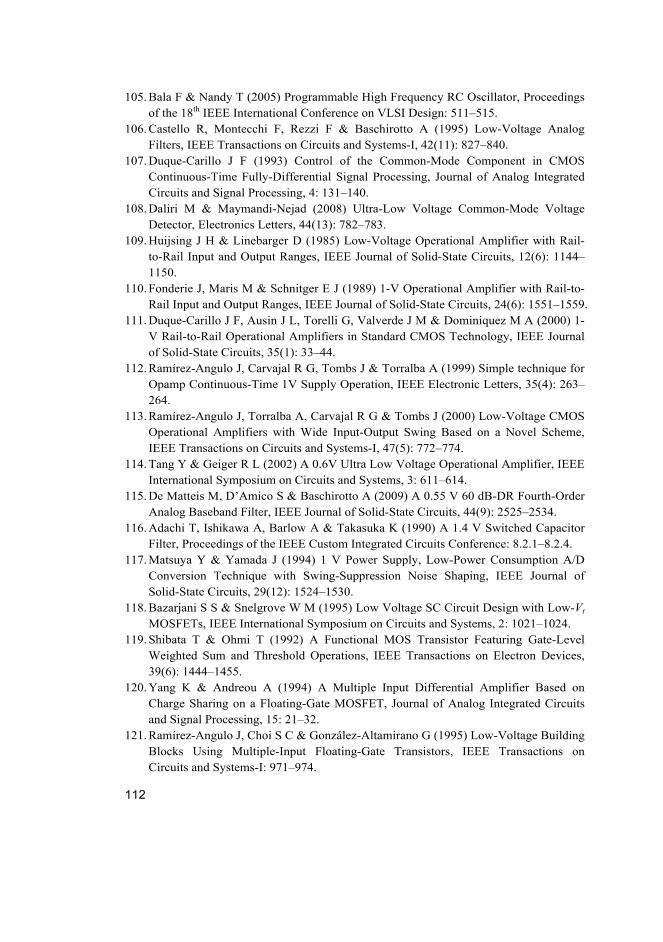
112
105. Bala F & Nandy T (2005) Programmable High Frequency RC Oscillator, Proceedings of the 18th IEEE International Conference on VLSI Design: 511–515.
106. Castello R, Montecchi F, Rezzi F & Baschirotto A (1995) Low-Voltage Analog Filters, IEEE Transactions on Circuits and Systems-I, 42(11): 827–840.
107. Duque-Carillo J F (1993) Control of the Common-Mode Component in CMOS Continuous-Time Fully-Differential Signal Processing, Journal of Analog Integrated Circuits and Signal Processing, 4: 131–140.
108. Daliri M & Maymandi-Nejad (2008) Ultra-Low Voltage Common-Mode Voltage Detector, Electronics Letters, 44(13): 782–783.
109. Huijsing J H & Linebarger D (1985) Low-Voltage Operational Amplifier with Rail-to-Rail Input and Output Ranges, IEEE Journal of Solid-State Circuits, 12(6): 1144–1150.
110. Fonderie J, Maris M & Schnitger E J (1989) 1-V Operational Amplifier with Rail-to-Rail Input and Output Ranges, IEEE Journal of Solid-State Circuits, 24(6): 1551–1559.
111. Duque-Carillo J F, Ausin J L, Torelli G, Valverde J M & Dominiquez M A (2000) 1-V Rail-to-Rail Operational Amplifiers in Standard CMOS Technology, IEEE Journal of Solid-State Circuits, 35(1): 33–44.
112. Ramírez-Angulo J, Carvajal R G, Tombs J & Torralba A (1999) Simple technique for Opamp Continuous-Time 1V Supply Operation, IEEE Electronic Letters, 35(4): 263–264.
113. Ramírez-Angulo J, Torralba A, Carvajal R G & Tombs J (2000) Low-Voltage CMOS Operational Amplifiers with Wide Input-Output Swing Based on a Novel Scheme, IEEE Transactions on Circuits and Systems-I, 47(5): 772–774.
114. Tang Y & Geiger R L (2002) A 0.6V Ultra Low Voltage Operational Amplifier, IEEE International Symposium on Circuits and Systems, 3: 611–614.
115. De Matteis M, D’Amico S & Baschirotto A (2009) A 0.55 V 60 dB-DR Fourth-Order Analog Baseband Filter, IEEE Journal of Solid-State Circuits, 44(9): 2525–2534.
116. Adachi T, Ishikawa A, Barlow A & Takasuka K (1990) A 1.4 V Switched Capacitor Filter, Proceedings of the IEEE Custom Integrated Circuits Conference: 8.2.1–8.2.4.
117. Matsuya Y & Yamada J (1994) 1 V Power Supply, Low-Power Consumption A/D Conversion Technique with Swing-Suppression Noise Shaping, IEEE Journal of Solid-State Circuits, 29(12): 1524–1530.
118. Bazarjani S S & Snelgrove W M (1995) Low Voltage SC Circuit Design with Low-Vt MOSFETs, IEEE International Symposium on Circuits and Systems, 2: 1021–1024.
119. Shibata T & Ohmi T (1992) A Functional MOS Transistor Featuring Gate-Level Weighted Sum and Threshold Operations, IEEE Transactions on Electron Devices, 39(6): 1444–1455.
120. Yang K & Andreou A (1994) A Multiple Input Differential Amplifier Based on Charge Sharing on a Floating-Gate MOSFET, Journal of Analog Integrated Circuits and Signal Processing, 15: 21–32.
121. Ramírez-Angulo J, Choi S C & González-Altamirano G (1995) Low-Voltage Building Blocks Using Multiple-Input Floating-Gate Transistors, IEEE Transactions on Circuits and Systems-I: 971–974.
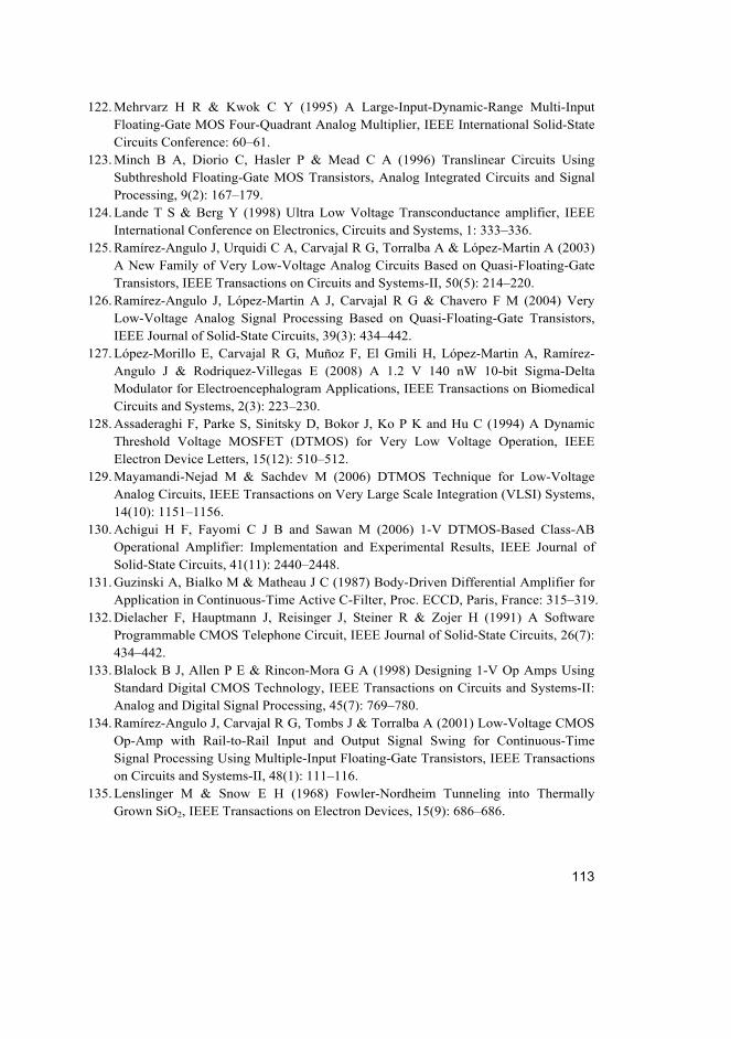
113
122. Mehrvarz H R & Kwok C Y (1995) A Large-Input-Dynamic-Range Multi-Input Floating-Gate MOS Four-Quadrant Analog Multiplier, IEEE International Solid-State Circuits Conference: 60–61.
123. Minch B A, Diorio C, Hasler P & Mead C A (1996) Translinear Circuits Using Subthreshold Floating-Gate MOS Transistors, Analog Integrated Circuits and Signal Processing, 9(2): 167–179.
124. Lande T S & Berg Y (1998) Ultra Low Voltage Transconductance amplifier, IEEE International Conference on Electronics, Circuits and Systems, 1: 333–336.
125. Ramírez-Angulo J, Urquidi C A, Carvajal R G, Torralba A & López-Martin A (2003) A New Family of Very Low-Voltage Analog Circuits Based on Quasi-Floating-Gate Transistors, IEEE Transactions on Circuits and Systems-II, 50(5): 214–220.
126. Ramírez-Angulo J, López-Martin A J, Carvajal R G & Chavero F M (2004) Very Low-Voltage Analog Signal Processing Based on Quasi-Floating-Gate Transistors, IEEE Journal of Solid-State Circuits, 39(3): 434–442.
127. López-Morillo E, Carvajal R G, Muñoz F, El Gmili H, López-Martin A, Ramírez-Angulo J & Rodriquez-Villegas E (2008) A 1.2 V 140 nW 10-bit Sigma-Delta Modulator for Electroencephalogram Applications, IEEE Transactions on Biomedical Circuits and Systems, 2(3): 223–230.
128. Assaderaghi F, Parke S, Sinitsky D, Bokor J, Ko P K and Hu C (1994) A Dynamic Threshold Voltage MOSFET (DTMOS) for Very Low Voltage Operation, IEEE Electron Device Letters, 15(12): 510–512.
129. Mayamandi-Nejad M & Sachdev M (2006) DTMOS Technique for Low-Voltage Analog Circuits, IEEE Transactions on Very Large Scale Integration (VLSI) Systems, 14(10): 1151–1156.
130. Achigui H F, Fayomi C J B and Sawan M (2006) 1-V DTMOS-Based Class-AB Operational Amplifier: Implementation and Experimental Results, IEEE Journal of Solid-State Circuits, 41(11): 2440–2448.
131. Guzinski A, Bialko M & Matheau J C (1987) Body-Driven Differential Amplifier for Application in Continuous-Time Active C-Filter, Proc. ECCD, Paris, France: 315–319.
132. Dielacher F, Hauptmann J, Reisinger J, Steiner R & Zojer H (1991) A Software Programmable CMOS Telephone Circuit, IEEE Journal of Solid-State Circuits, 26(7): 434–442.
133. Blalock B J, Allen P E & Rincon-Mora G A (1998) Designing 1-V Op Amps Using Standard Digital CMOS Technology, IEEE Transactions on Circuits and Systems-II: Analog and Digital Signal Processing, 45(7): 769–780.
134. Ramírez-Angulo J, Carvajal R G, Tombs J & Torralba A (2001) Low-Voltage CMOS Op-Amp with Rail-to-Rail Input and Output Signal Swing for Continuous-Time Signal Processing Using Multiple-Input Floating-Gate Transistors, IEEE Transactions on Circuits and Systems-II, 48(1): 111–116.
135. Lenslinger M & Snow E H (1968) Fowler-Nordheim Tunneling into Thermally Grown SiO2, IEEE Transactions on Electron Devices, 15(9): 686–686.
114
136. Thomsen A & Brooke M (1991) A Floating-Gate MOSFET with Tunneling Injector Fabricated Using a Standard Double-Silicon CMOS Process, IEEE Electron Device Letters, 12(3): 111–113.
137. Jackson S A, Killens J C, Blalock B J (2001) A Programmable Current Mirror for Analog Trimming Using Single-Poly Floating-Gate Devices in Standard CMOS Technology, IEEE Transactions on Circuits and Systems-II, 48(1): 100–102.
138. Kotani K, Shibata T, Imai M & Ohmi T (1998) Clock-Controlled Neuron-MOS Logic Gates, IEEE Transactions on Circuits and Systems-II, 45(4): 518–522.
139. Rodriguez-Villegas E & Barnes H (2003) Solution to Trapped Charge in FGMOS Transistors, IEEE Electronic Letters, 39(19): 1416–1417.
140. Gerber B, Martin J-C & Fellrath J (1981) A 1.5V Single-Supply One-Transistor CMOS EEPROM, IEEE Journal of Solid-State Circuits, 16(3): 195–200.
141. Dickson J F (1976) On-Chip High-Voltage Generation in MNOS Integrated Circuits Using an Improved Voltage Multiplier Technique, IEEE Journal of Solid-State Circuits, 11(3): 374–378.
142. Callias F, Salchli F H & Girard D (1989) A Set of Four IC’s in CMOS Technology for a Programmable Hearing Aid, IEEE Journal of Solid-State Circuits, 24(2): 301–312.
143. Nakagome Y, Tanaka H, Takeuchi K, Kume E, Watanabe Y, Kaga T, Kawamoto Y, Murai F, Izawa R, Hisamoto D, Kisu T, Nishida T, Takeda E & Itoh K (1991) An Experimental 1.5-V 64-Mb DRAM, IEEE Journal of Solid-State Circuits, 26(4): 465–472.
144. Wu J-T, Chang Y-H & Chang K-L (1998) 1.2 V CMOS Switched-Capacitor Circuits, IEEE International Solid-State Circuits Conference: 388–389.
145. Abo A M (1999) Design for Reliability of Low-Voltage, Switched-Capacitor Circuits. PhD thesis, University of California, Berkeley.
146. Dessouky M & Kaiser A (1999) Input Switch Configuration Suitable for Rail-to-Rail Operation of Switched Opamp Circuits, IEEE Electronic Letters, 35(1): 8–10.
147. Steensgaard J (1999) Bootstrapped Low-Voltage Analog Switches, Proceedings of the IEEE International Symposium on Circuits and Systems (ISCAS), 2: 29–32.
148. Dessouky M & Kaiser A (2001) Very Low-Voltage Digital-Audio ΔΣ Modulator with 88-dB Dynamic Range Using Local Switch Bootstrapping, IEEE Journal of Solid-State Circuits, 36(3): 349–355.
149. Muñoz F, Ramírez-Angulo J, Lopez-Martin A, Carvajal R G, Torralba A, Palomo B & Kachare M (2003) Analogue Switch for Very Low-Voltage Applications, IEEE Electronic Letters, 39(9): 701–702.
150. Aksin D, Al-Shyoukh M & Maloberti F (2006) Switch Bootstrapping for Precise Sampling Beyond Supply Voltage, IEEE Journal of Solid-State Circuits, 41(8): 1938–1943.
151. Crols J & Steyaert M (1994) Switched-Opamp: An Approach to Realize Full CMOS Switched-Capacitor Circuits at Very Low Power Supply Voltages, IEEE Journal of Solid-State Circuits, 29(8): 936–942.
152. Baschirotto A, Castello R & Montecchi F (1994) Design Strategy for Low-Voltage SC Circuits, IEEE Electronic Letters, 30(5): 378–380.
115
153. Baschirotto A & Castello R (1997) A 1-V 1.8 MHz CMOS Switched-Opamp SC Filter with Rail-to-Rail Output Swing, IEEE Journal of Solid-State Circuits, 32(12): 1979–1997.
154. Peluso V, Vancorenland P, Steyaert M & Sansen W (1997) 900 mV Differential Class AB OTA for Switched Opamp Applications, IEEE Electronic Letters, 33(17): 1455–1456.
155. Peluso V, Vancorenland P, Marques A M, Steyaert M S J & Sansen W (1998) A 900-mV Low-Power ΔΣ A/D Converter with 77-dB Dynamic Range, IEEE Journal of Solid-State Circuits, 33(12): 1887–1897.
156. Baschirotto A, Bijno D, Castello R & Montecchi F (2000) A 1V 1.2 μW 4th Order Bandpass Switched-Opamp SC filter for a Cardiac Pacer Sensing Stage, IEEE International Symposium on Circuits and Systems (ISCAS), 3:173–176.
157. Waltari M & Halonen K (2001) 1-V 9-bit Pipelined Switched-Opamp ADC, IEEE Journal of Solid-State Circuits, 36(1): 129–134.
158. Baschirotto A, Castello R & Montagna G P (1998) Active Series Switch for Switched-Opamp Circuits, IEEE Electronic Letters, 34(14): 1365–1366.
159. Waltari M & Halonen K (1999) An 8-bit Low-Voltage Pipelined ADC Utilizing Switched-Opamp Technique, Proceedings of the 25th European Solid-State Circuits Conference: 174–177.
160. Karthikeyan S, Tamminneedi A, Boecker C & Lee E K F (2001) Design of Low-Voltage Front-End Interface for Switched-Opamp Circuits, IEEE Transactions on Circuits and Systems-II, 48(7): 722–726.
161. Bonfini G, Brogna A S, Garbossa C, Colombini L, Bacci M, Chicca S, Bigongiari F, Guerrini N C & Ferri G (2004) An Ultralow-Power Switched Opamp-Based 10-B Integrated ADC for Implantable Biomedical applications, IEEE Transactions on Circuits and Systems-I, 51(1): 174–178.
162. Abo A M & Grey P R (1999) A 1.5-V 10-bit, 14.3-MS/s CMOS Pipeline Analog-to-Digital Converter, IEEE Journal of Solid-State Circuits, 34(5): 599–606.
163. Wu P Y, Cheung V S-L & Luong H C (2007) A 1-V 100-MS/s 8-bit CMOS Switched-Opamp Pipelined ADC Using Loading-Free Architecture, IEEE Journal of Solid-State Circuits, 34(5): 730–738.
164. Säckinger E & Guggenbuhl W (1987) A Versatile Building Block: The CMOS Differential Difference Amplifier, IEEE Journal of Solid-State Circuits, 22(2): 287–294.
165. Winter B B & Webster J G (1983) Driven-Right-Leg Circuit Design, IEEE Transactions on Biomedical Engineering, 30(1): 62–66.
166. Steyaert M S J, Sansen W M C and Zhongyuan C (1987) A Micropower Low-Noise Monolithic Instrumentation Amplifier for Medical Purposes, IEEE Journal of Solid-State Circuits, 22(6): 1163–1168.
167. Inan O T & Kovacs T A (2010) An 11 µW, Two-Electrode Transimpedance Biosignal Amplifier With Active Current Feedback Stabilization, IEEE Transactions on Biomedical Circuits and Systems, 4(1): 93–100.
116
168. Martins R, Selberherr S & Vaz F A (1998) A CMOS IC for Portable EEG Acquisition Systems, IEEE Transactions on Instrumentation and Measurement, 47(5): 1191–1196.
169. Mohseni P & Najafi K (2004) A Fully Integrated Neural Recording Amplifier With DC Input Stabilization, IEEE Transactions on Biomedical Engineering, 51(5): 832–837.
170. Horiuchi T, Swindell T, Sander D & Abshire P (2004) A Low-Power CMOS Neural Amplifier With Amplitude Measurements for Spike Sorting, IEEE International Conference on Circuits and Systems 4: 29–32.
171. Olsson R H, Buhl D L, Sirota A M, Buzsaki G & Wise K D (2005) Band-Tunable and Multiplexed Integrated Circuits for Simultaneous Recording and Stimulation With Microelectrode Arrays, IEEE Transactions on Biomedical Engineering, 52(7): 1303–1311.
172. Chan C-H, Wills J, LaCoss J, Granacki J J & Choma J (2006) A Micro-Power Low-Noise Auto-Zeroing CMOS Amplifier for Cortical Neural Prostheses, IEEE Biomedical Circuits and Systems Conference: 214–217.
173. Wattanapanitch W, Fee M & Sarpeshkar R (2007) An Energy-Efficient Micropower Neural Recording Amplifier, IEEE Transactions on Biomedical Circuits and Systems, 1(2): 136–147.
174. Cheung V S L & Luong F C (2003) A 0.9V 0.5μW CMOS Single-Switched-Op-amp Signal Conditioning System for Pacemaker Applications, IEEE International Solid-State Conference 1: 408–409.
175. Chiang J-S, Chen H-P & Ying C-M (2003) A 1V 0.54μW Fourth order Switched Capacitor Filter with Switched Opamp Technique for Cardiac Pacemaker Sensing Channel, IEEE International Conference on Circuits and Systems 1: 481–484.
176. Corbishley P & Rodriguez-Villegas E (2007) IEEE Transactions on Biomedical Circuits and Systems 1(3): 163–171.
177. Lee S-Y & Cheng C-J (2009) Systematic Design and Modeling of a OTA-C Filter for Portable ECG Detection, IEEE Transactions on Biomedical Circuits and Systems 3(1): 53–64.
178. Johnson M & Hudson E (1988) A Variable Delay Line PLL for CPU-Coprocessor Synchronization, IEEE Journal of Solid-State Circuits, 23(5): 1218–1223.
117
Original papers
I Räisänen-Ruotsalainen E, Lasanen K & Kostamovaara J (2000) A 1.2 V Micropower CMOS Op Amp with Floating-Gate Input Transistors, Proceedings of the 43rd IEEE Midwest Symposium on Circuits and Systems, Lansing, Michigan, USA, August 2000, 2: 794–797.
II Lasanen K, Räisänen-Ruotsalainen E & Kostamovaara J (2000) A 1-V 5µW CMOS-Opamp with Bulk-Driven Input Transistors, Proceedings of the 43rd IEEE Midwest Symposium on Circuits and Systems, Lansing, Michigan, USA, August 2000, 3: 1038–1041.
III Räisänen-Ruotsalainen E, Lasanen K, Siljander M & Kostamovaara J (2002) A Low-Power 5.4 kHz CMOS gm-C Bandpass Filter with On-Chip Center Frequency Tuning, Proceedings of the 2002 IEEE International Symposium on Circuits and Systems, Phoenix, Arizona, U.S.A., May 2002, 4: 651–654.
IV Lasanen K, Räisänen-Ruotsalainen E & Kostamovaara J (2002) A 1-V, Self Adjusting, 5-MHz CMOS RC-Oscillator, Proceedings of the 2002 IEEE International Symposium on Circuits and Systems, Phoenix, Arizona, U.S.A., May 2002, 4: 377–380.
V Lasanen K, Korkala V, Räisänen-Ruotsalainen E & Kostamovaara J (2002) Design of a 1-V Low-Power CMOS Bandgap Reference Based on Resistive Subdivision, Proceedings of the 45th IEEE Midwest Symposium on Circuits and Systems, Tulsa, Oklahoma, USA, August 2002, 3: 564–567.
VI Lasanen K & Kostamovaara J (2004) A 1-V CMOS Preprocessing Chip for ECG Measurements, Proceedings of the IEEE International Workshop on BioMedical Circuits & Systems, Singapore, December 2004: S1/2 - S1-4.
VII Lasanen K & Kostamovaara J (2005) A 1-V Analog CMOS Front-End for Detecting QRS Complexes in a Cardiac Signal, IEEE Transactions on Circuits and Systems-I, December 2005, 52(12): 2584–2594.
VIII Lasanen K & Kostamovaara J (2008) A 1.2-V CMOS RC Oscillator for Capacitive and Resistive Sensor Applications, IEEE Transactions on Instrumentation and Measurements, December 2008, 57(12): 2792–2800.
Reprinted with permission from The Institute of Electrical and Electronics
Engineers, Incorporated (IEEE).
Original publications are not included in the electronic version of the dissertation.

118
A C T A U N I V E R S I T A T I S O U L U E N S I S
Book orders:Granum: Virtual book storehttp://granum.uta.fi/granum/
S E R I E S C T E C H N I C A
366. Palukuru, Vamsi Krishna (2010) Electrically tunable microwave devices using BST-LTCC thick films
367. Saarenpää, Ensio (2010) Rakentamisen hyvä laatu : rakentamisen hyvän laaduntoteutuminen Suomen rakentamismääräyksissä
368. Vartiainen, Johanna (2010) Concentrated signal extraction using consecutivemean excision algorithms
369. Nousiainen, Olli (2010) Characterization of second-level lead-free BGAinterconnections in thermomechanically loaded LTCC/PWB assemblies
370. Taskila, Sanna (2010) Improved enrichment cultivation of selected food-contaminating bacteria
371. Haapala, Antti (2010) Paper machine white water treatment in channel flow :integration of passive deaeration and selective flotation
372. Plekh, Maxim (2010) Ferroelectric performance for nanometer scaled devices
373. Lee, Young-Dong (2010) Wireless vital signs monitoring system for ubiquitoushealthcare with practical tests and reliability analysis
374. Sillanpää, Ilkka (2010) Supply chain performance measurement in themanufacturing industry : a single case study research to develop a supply chainperformance measurement framework
375. Marttila, Hannu (2010) Managing erosion, sediment transport and water quality indrained peatland catchments
376. Honkanen, Seppo (2011) Tekniikan ylioppilaiden valmistumiseen johtavienopintopolkujen mallintaminen — perusteena lukiossa ja opiskelun alkuvaiheessasaavutettu opintomenestys
377. Malinen, Ilkka (2010) Improving the robustness with modified boundedhomotopies and problem-tailored solving procedures
378. Yang, Dayou (2011) Optimisation of product change process and demand-supplychain in high tech environment
379. Kalliokoski, Juha (2011) Models of filtration curve as a part of pulp drainageanalyzers
380. Myllylä, Markus (2011) Detection algorithms and architectures for wireless spatialmultiplexing in MIMO-OFDM systems
381. Muhos, Matti (2011) Early stages of technology intensive companies
C383etukansi.kesken.fm Page 2 Wednesday, May 4, 2011 1:58 PM
ABCDEFG
UNIVERS ITY OF OULU P.O.B . 7500 F I -90014 UNIVERS ITY OF OULU F INLAND
A C T A U N I V E R S I T A T I S O U L U E N S I S
S E R I E S E D I T O R S
SCIENTIAE RERUM NATURALIUM
HUMANIORA
TECHNICA
MEDICA
SCIENTIAE RERUM SOCIALIUM
SCRIPTA ACADEMICA
OECONOMICA
EDITOR IN CHIEF
PUBLICATIONS EDITOR
Senior Assistant Jorma Arhippainen
Lecturer Santeri Palviainen
Professor Hannu Heusala
Professor Olli Vuolteenaho
Senior Researcher Eila Estola
Director Sinikka Eskelinen
Professor Jari Juga
Professor Olli Vuolteenaho
Publications Editor Kirsti Nurkkala
ISBN 978-951-42-9454-9 (Paperback)ISBN 978-951-42-9455-6 (PDF)ISSN 0355-3213 (Print)ISSN 1796-2226 (Online)
U N I V E R S I TAT I S O U L U E N S I SACTAC
TECHNICA
U N I V E R S I TAT I S O U L U E N S I SACTAC
TECHNICA
OULU 2011
C 383
Kimmo Lasanen
INTEGRATED ANALOGUE CMOS CIRCUITS AND STRUCTURES FOR HEART RATE DETECTORS AND OTHER LOW-VOLTAGE, LOW-POWER APPLICATIONS
UNIVERSITY OF OULU,FACULTY OF TECHNOLOGY,DEPARTMENT OF ELECTRICAL AND INFORMATION ENGINEERING;UNIVERSITY OF OULU,INFOTECH OULU
C 383
ACTA
Kim
mo Lasanen
C383etukansi.kesken.fm Page 1 Wednesday, May 4, 2011 1:58 PM