two low power and high efficient full adder cells based on ... no... · full adder circuit with 19...
TRANSCRIPT
International Journal of Nanoelectronics and Materials Volume 11, No. 3, July 2018 [321-332]
Two Low Power and High Efficient Full Adder Cells Based on CNTFET Technology
Masoud Farahani1 and Mona Moradi2*
1Department of Computer Engineering, Roudehen Branch, Islamic Azad University, Roudehen, Iran.
2Roudehen Branch, Islamic Azad University, Roudehen, Iran.
Received 27 October 2017; Revised 21 December 2017; Accepted 16 January 2018
ABSTRACT
This paper presents two novel full adder cells based on Carbon Nanotube Field Effect Transistor (CNTFET) technology. According to unique specifications of CNTFET, and its similarity to conventional MOSFET technology, CNTFET technology is considered as a good successor for conventional MOSFET technology in nano-electronic in near future. The full adder cells benefit from less power consumption, delay time and occupied area comparing to peer designs. All CNTFET presented and previous designs have been carried out using Synopsys HSPICE in a realistic test bench and other various strict conditions in 32 nm technology. The Simulation results show that presented adders perform better comparing the previous designs.
Keywords: CNTFET, Full Adder, High-Speed, High-Frequency, Nanoelectronics
1. INTRODUCTION
Full adder is among the greatest useful logic blocks, it is considered as the key arithmetical
component of all digital systems [1]. Several operations like multiplying, subtraction, division
and arithmetic operators are done by means of addition [2]. In a nutshell, the full adder cell and
its output signals exclusively are among the most practical logic blocks in VLSI circuits. The
critical path of almost all digital systems includes full adder blocks [1].in case being improving
the adder cell performance can improve the whole system consequently.
Complementary Metal Oxide Semiconductor processors (CMOS) have been dominant technology for many decades. Nowadays many applications such as telecommunications, transportation, education and medical care are dependent on the technology (CMOS) [3]. Meanwhile the needs of scaling down the size of transistors brought many challenges and difficulties for circuit designers. Some of these challenges include very high leakage currents, decreasing the gate control, high power density, large parametric variations, and high lithography costs [4].
To overcome of these problems, some technologies have been presented previously like: Carbon Nanotube Field Effect Transistor (CNTFET), Single Electron Transistor (SET), Graphene Nanoribbon Transistor (GNRT), and Quantum Carbon Automata (QCA) [5, 6, and 7].
However, CNTFET technology because of its unique characteristics such as Ballistic transport ability which brings about high-speed operation, same mobility for both nCNTFET and pCNTFET types which directs to simple transistor sizing process, and the ability of adjusting
Corresponding Author: [email protected]

Masoud farahani and Mona Moradi / Two Low Power and High Efficient Full…
322
desired threshold voltage by adopting proper diameter for the nanotubes(Eq.1, 2), are definitely worth to discussion[7].
Figure 1. (a) A typical CNTFET device; Different types of CNTFET device (b) SB-CNTFET (c) MOSFET-like
CNTFET(d) T-CNTFET [7].
2 2
1 2 1 20.0783CNTD n n n n (1)
3 0.43
2 3
g
t
CNT CNT
E EV
e eD D
(2)
In this paper, two novel 1-bit high-speed and high-efficient full adder cells are presented. The proposed designs are based on pass transistor logic. The Sum and Cout signals are generated separately. The key target is to achieve high performance and high efficiency while the proposed design has the advantage of full voltage swing outputs, high driving power, robustness and the ability of employed in high frequencies and low voltages. Different conventional full adder cells with the same logic style have been selected for evaluation. High speed, low power consumption, and novelty are the main issues which make the presented designs an ideal selection. All circuits are simulated with HSPICE and 32 nm CNTFET technology in a realistic environment and other various conditions. The simulation results reveal the superiority of the proposed design. The rest of the paper is prepared as follows: In Section 2, previous researches are reviewed. Proposed design will be presented in Section 3. Section 4 contains simulation results. Finally, Section 5 covers conclusion. 2. PREVIOUS RESEARCH
Figure 2 demonstrated a 23 T full adder cell [8]. The design is a combination of transmission gate and pass-transistor logic. The inverted outputs are first generated. Formerly, two inverters are utilized for final conversion. In spite of adding extra transistors and increasing longer critical path, it brings about higher speed and driving capability in case of existing high number of fan-outs. The intermediate XOR and XNOR functions are not generated in a parallel manner which leads to longer critical path within the cell. A multiplexer-based structure is used to generate the other output signal (Cout) [1].

International Journal of Nanoelectronics and Materials Volume 11, No. 3, July 2018 [321-332]
323
Figure 2. 23T full adder cell presented in [8].
Figure 3 shows a hybrid full adder cell [9]. Two different circuits are used to generate output signals simultaneously. The Sum output is generated by means of two different cascaded XOR/XNOR cells. The first cell is a pseudo-DCVS circuit which generates both functions using only 6 transistors. The following one is a high speed DCVS circuit. It can produce both sum and sumnot. However, an inverted input is required for the 2nd stage, albeit the cell arrangement eliminates using extra inverter. Hence, complementary inputs are not essential within the whole cell. Though, long critical path together and a low driving capability of the DCVS structure leads to low speed. The last inverters are added to decrease the delay particularly while driving high load capacitors. To generate the Cout the bridge style architecture is employed [9].
Figure 3. Hybrid full adder cell presented in [9].
The CNT-CPL designed discussed in figure 4 creates an adder block uniquely [10]. Its critical path includes only two pass transistors. In addition, designing based on CNTFET technology brings higher speed, and can overcoming the drawback of non-full-swing nodes [10]. However, low driving capability is the main disadvantage of the cell because of the applied pass-transistor logic. Although it is possible to implement the inverted outputs and use inverters to obtain higher driving power, however its lead to higher transistor counts [10]. In addition, cascading blocks in serial manner causes signal distortion especially in high frequencies. Finally, the same structures are used for both Sum and Cout [1].

Masoud farahani and Mona Moradi / Two Low Power and High Efficient Full…
324
Figure 4. CNT-CPL full adder cell presented in [10].
The last investigated full adder cell is another CNTFET-based circuit represented CNTFA (Figure 5) [11]. This is also based on intermediate XOR and XNOR functions and pass-transistor logic. The generated XOR/XNOR outputs are employed as selectors in a multiplexer-based structure at the 2nd stage to generate Sum. Another pass-transistor based block at the 2nd stage is utilized to generate the COUT in parallel with Sum. The designs benefit from full-swing operation, low power consumption and high-speed computation. However, it suffers from low driving capability [1].
Figure 5. CNTFA cell presented in [11].
3. PROPOSED FULL ADDER CELL
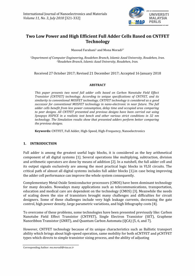
Figure 6 show the 1st presented design includes 19 transistors. In this design the elimination of using the invetred values of both input (ANOT, BNOT) signals lead to less number of transistor and less occupied area. One XOR unit is employed to omit the use of the inverters. So, the critical path of the design has decreased. This can improve the delay time and also the power delay product (PDP).
International Journal of Nanoelectronics and Materials Volume 11, No. 3, July 2018 [321-332]
325
Figure 6. Full adder circuit with 19 transistors (19T proposed).
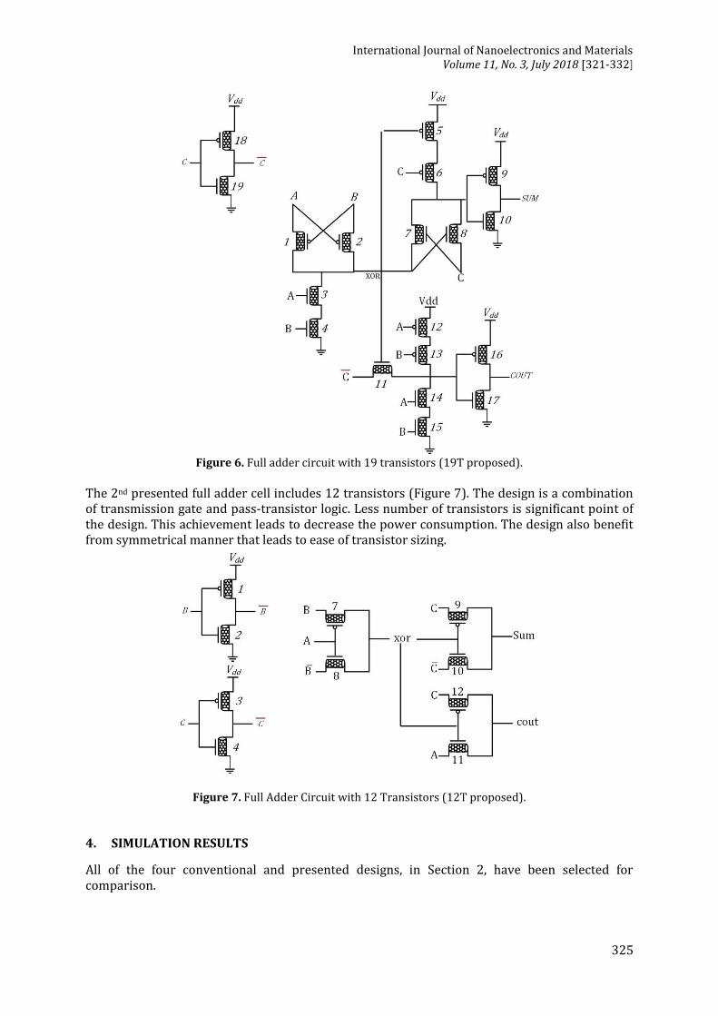
The 2nd presented full adder cell includes 12 transistors (Figure 7). The design is a combination of transmission gate and pass-transistor logic. Less number of transistors is significant point of the design. This achievement leads to decrease the power consumption. The design also benefit from symmetrical manner that leads to ease of transistor sizing.
Figure 7. Full Adder Circuit with 12 Transistors (12T proposed).
4. SIMULATION RESULTS
All of the four conventional and presented designs, in Section 2, have been selected for comparison.

Masoud farahani and Mona Moradi / Two Low Power and High Efficient Full…
326
The choice of each circuit is based on its features such as high speed, low power, novelty, and structural similarity to the presented designs. The proposed design and the other full adder cells have been simulated with Synopsys HSPICE and 32 nm CNTFET technology [11]. Input Buffers together with a 2fF load capacitor have been applied to make a practical condition for all presented and previous designs. Transistor sizing details for both proposed designs are shown in table 1 and 2.
Table 1 CNT circuit proposed with 19 Transistors
Transistors DCNT(nm) #CNTs
1,2 2.7405 10 3,4 2.2707 3 5,6 1.4877 3 7,8 2.7405 5
9,10 1.4877 16 18,19 1.4877 5
Table 2 CNT circuit proposed with 12 Transistors
Transistors DCNT(nm) #CNTs
1 to 4 1.4877 5 7 and 8 4.5414 4
9 3.8367 3 10 3.6018 4
11 and 12 2.7405 3 13 and 14 1.8009 9
The simulation results are shown in Table 3. The simulation has been carried out at 0.7V power supply with 100MHz operating frequency at room temperature. Table 3 Simulation results all circuits at room temprature and 0.7 supply voltage and 100 MHz operating
frequency
Delay(psec) Power(μW) PDP(aJ) Type
17.45 0.19186 3.3479 19T proposed 21.651 0.19812 4.2895 12T proposed
The complete input pattern [1] with 56 transitions has been fed to measure the delay of each cell. In order to show the worst delay, all possible transitions in this input pattern have been checked [11]. The delay parameter has been considered from the time that the input signal reaches Vdd to the time that the output signal touches the same voltage level. The maximum delay of all transitions is considered as a cell delay. The average power consumption during all transitions is called as the power consumption parameter. Finally, the PDP, which creates a balance between delay and power, is calculated. PDP= delay * power (3)
The proposed full adder cells show better performance comparing peer designs. The simulation has been carried out at 0.9 V, 0.8 V, and 0.7 V power supplies with 100 MHz operating frequency at room temperature (Table 4).

International Journal of Nanoelectronics and Materials Volume 11, No. 3, July 2018 [321-332]
327
Table 4 Simulation results at room temprature and 100 MHz operating frequency versus different supply voltages
0.9 V 0.8 V 0.7 V Vdd
Delay(psec) 115.4 145.79 205.23 23T Full Adder cell [8]
113.58 142.42 252.58 Hybrid Full Adder [9] 27.376 30.267 33.854 CNT-CPL Full Adder Cell [10] 25.393 28.872 35.486 CNTFA Cell [11] 16.203 17.45 21.112 19T proposed 18.787 21.651 25.517 12T proposed
Power (µW) 0.4459 0.3122 0.2219 23T Full Adder cell [8] 0.5403 0.3683 0.2633 Hybrid Full Adder [9] 0.6512 0.3138 0.2326 CNT-CPL Full Adder Cell [10] 0.2630 0.2011 0.1518 CNTFA Cell [11]
0.25769 0.19186 0.16019 19T proposed 0.24879 0.19812 0.15627 12T proposed
PDP (aJ) 51.457 45.574 45.542 23T Full Adder cell [8] 61.374 52.456 66.494 Hybrid Full Adder [9] 17.828 9.4986 7.8739 CNT-CPL Full Adder Cell [10] 6.6792 5.8057 5.3679 CNTFA Cell [11] 4.1755 3.3479 3.382 19T proposed 4.674 4.2895 3.9875 12T proposed
The proposed cells have the less delay among the compared adders presented in Table 4. For instance, 12T and 19T designs are 25.01% and 28.26% faster than The CNTFA Cell which is the fastest cell among the adders. Another characteristic of driving capability is the ability of working in larger circuits. So, three cascaded cells have been studied as the second simulation setup (Figure 8). The Sum signal in the 1st possible cascading test-bed (Figure 8(a)), the Sum is considered as both the first and the second inputs of the following cell, however the Cout signal is the 3rd one. Concerning Eq. 1 and Eq. 2, the duplication of Sum leads to a swap in the wave forms of former output signals. It worth to mention, there is not a swap in the waveforms by applying the 2nd cascading simulation setup (Figure 8(b)) as the Cout signal is repeated, (Eq. 3 and Eq. 4). Hence, an even number of cascaded cells is also possible to be comprehended.
Sum (Next Cell) = Sum Sum Cout = Cout (1) Cout (Next Cell) = Majority (Sum, Sum, Cout) = Sum (2) Sum (Next Cell) = Sum Cout Cout = Sum( (3) Cout (Next Cell) = Majority (Sum, Cout, Cout) = Cout (4)
(a)

Masoud farahani and Mona Moradi / Two Low Power and High Efficient Full…
328
(b)
Figure 8. Cascading simulation setups [10].
Input and output buffers are also in employment to make even more severe conditions. The output wave forms of the third cell are shown in Figure 9 for the proposed designs.
Figure 9. Output wave forms of the third cell for the proposed design.
Finally, Monte Carlo transient analysis with a number of 30 iterations for each simulation is analysed to examine sensitivity to process variation. A standard deviation in the range of 0.04 nm to 0.2 nm is measured for each diameter value [11]. The proposed designs work reliably in case of procees variation (Figure 10).
Figure 10. Output wave forms of Monte Carlo transient analysis.
To examine the immunity of the propsed designs to the ambient temperature noise and variations, all designs have also been simulated in a vast range of temperatures from 0oC to 70oC. The results are presented in Figure 11. In spite of temperature variation, the results show that the proposed designs have normal functionality. They also beat other designs in terms Of performance.

International Journal of Nanoelectronics and Materials Volume 11, No. 3, July 2018 [321-332]
329
Figure 11. PDP versus temperature variations.
Today, the capability of working in high frequencies in VLSI circuits is necessitated. In case being, all circuits are simulated at higher frequencies such as 500 MHz and 5 GHz. Figure 12 displays the cells performance versus frequency increments. It can be understood that the proposed structures have the best performance comparing other circuits at high frequency operation.
Figure 12. PDP versus different operating frequencies.
0
10
20
30
40
50
60
70
80
90
70 60 50 40 30 20 10 0
23T
Hybrid
CNTCPL
CNTFA
19 T Proposed
12T Proposed
PD
P(a
J)
Temperature(ºC)
0
50
100
150
200
250
300
350
400
450
1000 500 250 100
23T
Hybrid
CNTCPL
CNTFA
19T Proposed
12T Proposed
PD
P(a
J)
frequency(MHz)
Masoud farahani and Mona Moradi / Two Low Power and High Efficient Full…
330
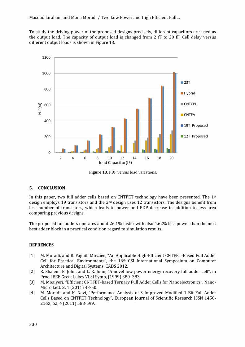
To study the driving power of the proposed designs precisely, different capacitors are used as the output load. The capacity of output load is changed from 2 fF to 20 fF. Cell delay versus different output loads is shown in Figure 13.
Figure 13. PDP versus load variations.
5. CONCLUSION
In this paper, two full adder cells based on CNTFET technology have been presented. The 1st design employs 19 transistors and the 2nd design uses 12 transistors. The designs benefit from less number of transistors, which leads to power and PDP decrease in addition to less area comparing previous designs. The proposed full adders operates about 26.1% faster with also 4.62% less power than the next best adder block in a practical condition regard to simulation results. REFRENCES [1] M. Moradi, and R. Faghih Mirzaee, “An Applicable High-Efficient CNTFET-Based Full Adder
Cell for Practical Environments”, the 16th CSI International Symposium on Computer Architecture and Digital Systems, CADS 2012.
[2] R. Shalem, E. John, and L. K. John, “A novel low power energy recovery full adder cell”, in Proc. IEEE Great Lakes VLSI Symp, (1999) 380–383.
[3] M. Moaiyeri, “Efficient CNTFET-based Ternary Full Adder Cells for Nanoelectronics”, Nano-Micro Lett. 3, 1 (2011) 43-50.
[4] M. Moradi, and K. Navi, “Performance Analysis of 3 Improved Modified 1-Bit Full Adder Cells Based on CNTFET Technology”, European Journal of Scientific Research ISSN 1450-216X, 62, 4 (2011) 588-599.
0
200
400
600
800
1000
1200
20 18 16 14 12 10 8 6 4 2
23T
Hybrid
CNTCPL
CNTFA
19T Proposed
12T Proposed
PD
P(a
J)
load Capacitor(fF)

International Journal of Nanoelectronics and Materials Volume 11, No. 3, July 2018 [321-332]
331
[5] M. Moaiyeri, R. Faghih Mirzaee, A. Doostaregan, K. Navi, & O. Hashemipour, “A universal method for designing low-power carbon nanotube FETbased multiple-valued logic circuits”, IET Computers & Digital Techniques, 7, 4 (2013) 167-181.
[6] K. Navi, S. Sayedsalehi, R. Farazkish and A. Mostafa Rahimi, “Five-input majority gate, a new device for quantum-dot cellular automata”, Journal of Computational and Theoretical Nanoscience, 7, 8 (2010) 1546-1553.
[7] K. Navi, M. Moaiyeri, & A. Momeni, “A low-voltage and energy-efficient full adder cell based on carbon nanotube technology”, Nano-Micro Letters, 2, 2 (2010) 114-120.
[8] H. Lee, G.E. And Sobelman, “New XOR/XNOR and full adder circuits for low voltage, low power applications”, Microelectronics Journal, 29 (1998) 519-517.
[9] R. Faghih Mirzaee, M.H. Moaiyeri, H. Khorsand, And K. Navi,“A new robust and high- erformance hybrid full adder cell”, Journal of Circuits,Systems, and Computers, 20, 4 (2011) 641-655.
[10] M.H. Moaiyeri, R. Faghih Mirzaee, K. Navi, and A. Momeni,“Design and analysis of a high-performance CNFET-based full adder”, International Journal of Electronics, 99, 1 (2012) 113-130.
[11] M.H. G hadiry, A.A. Manaf, M.T. Ahmadi, H. Sadeghi, and M.N. Senejani,“Design and Analysis of a New Carbon Nanotube Full Adder Cell”, Journal of Nanomaterials, Article ID.906237, 2011.
[12] L. Scheffer, the Count of Monte Carlo, “International Workshop on Timing Issues in the- Specification and”, Synthesis of Digital Systems, 2004.
