hw chapter 1. number systems/arithmetics · 2019-04-07 · 4.6 build a half-adder and a full-adder...
TRANSCRIPT
HW Chapter 1. Number Systems/Arithmetics
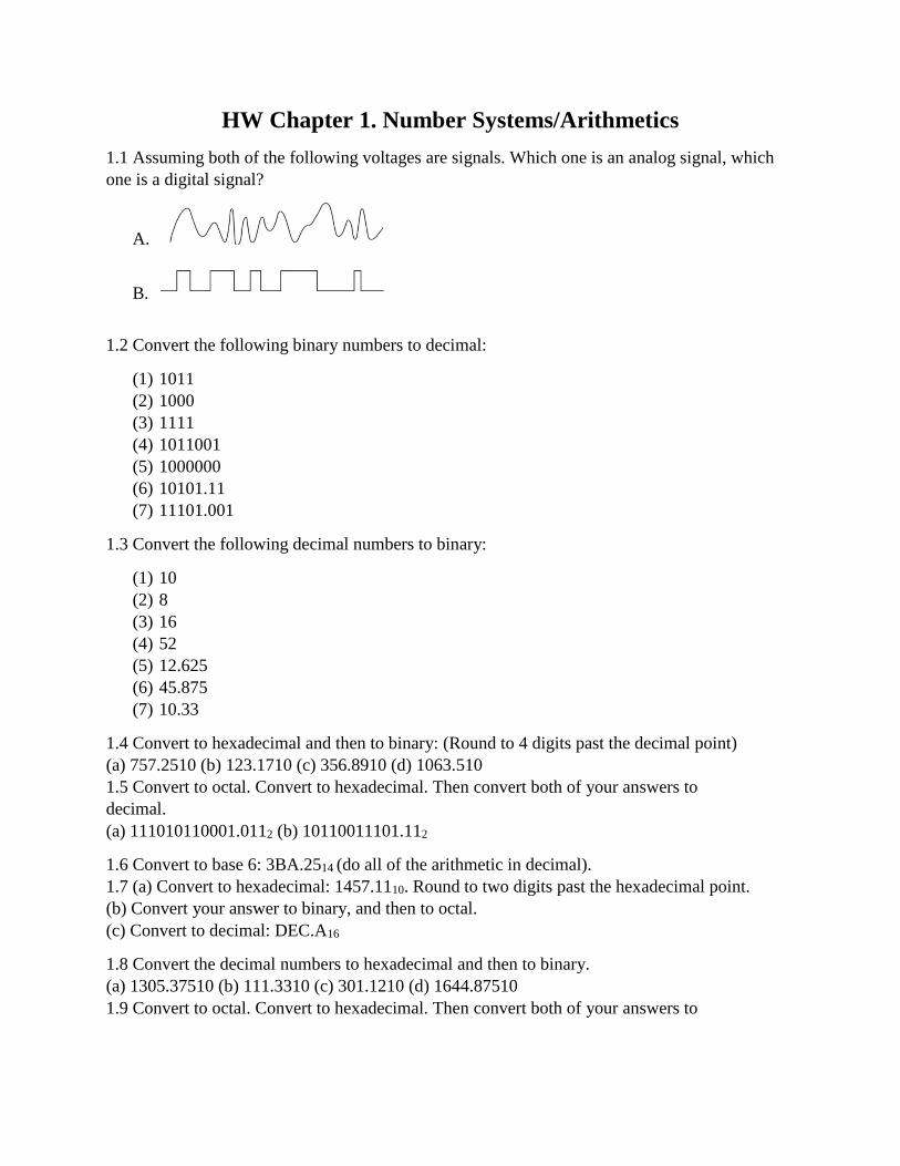
1.1 Assuming both of the following voltages are signals. Which one is an analog signal, which
one is a digital signal?
A.
B.
1.2 Convert the following binary numbers to decimal:
(1) 1011
(2) 1000
(3) 1111
(4) 1011001
(5) 1000000
(6) 10101.11
(7) 11101.001
1.3 Convert the following decimal numbers to binary:
(1) 10
(2) 8
(3) 16
(4) 52
(5) 12.625
(6) 45.875
(7) 10.33
1.4 Convert to hexadecimal and then to binary: (Round to 4 digits past the decimal point)
(a) 757.2510 (b) 123.1710 (c) 356.8910 (d) 1063.510
1.5 Convert to octal. Convert to hexadecimal. Then convert both of your answers to
decimal.
(a) 111010110001.0112 (b) 10110011101.112
1.6 Convert to base 6: 3BA.2514 (do all of the arithmetic in decimal).
1.7 (a) Convert to hexadecimal: 1457.1110. Round to two digits past the hexadecimal point.
(b) Convert your answer to binary, and then to octal.
(c) Convert to decimal: DEC.A16
1.8 Convert the decimal numbers to hexadecimal and then to binary.
(a) 1305.37510 (b) 111.3310 (c) 301.1210 (d) 1644.87510
1.9 Convert to octal. Convert to hexadecimal. Then convert both of your answers to
decimal, and verify that they are the same.
(a) 101111010100.1012 (b) 100001101111.012
1.10 Add, subtract, and multiply in binary:
(a) 1111 and 1010 (b) 110110 and 11101 (c) 100100 and 10110
1.11 Subtract in binary. Place a 1 over each column from which it was necessary to borrow.
(a) 11110100-1000111 (b) 1110110-111101 (c) 10110010-111101
1.12 Add, subtract, and multiply in binary:
(a) 1111 and 1001 (b) 1101001 and 110110 (c) 110010 and 11101
1.13 Subtract in binary. Place a 1 over each column from which it was necessary to borrow.
(a) 10100100-01110011 (b) 10010011-01011001
(c) 11110011-10011110
1.14 Divide in binary:
(a) 11101001/101 (b) 110000001/1110 (c) 1110010/1001
Check your answers by multiplying out in binary and adding the remainder.
1.15 Divide in binary:
(a) 10001101/110 (b) 110000011/1011 (c) 1110100/1010
1.16 Assume three digits are used to represent positive integers and also assume the following
operations are correct. Determine the base of the numbers. Did any of the
additions overflow?
(a) 654+013=000
(b) 024+043+013+033=223
(c) 024+043+013+033=201
1.17 Add the following numbers in binary using 2’s complement to represent negative numbers.
Indicate if an overflow occurs.
(a) 21+11 (b) (-14)+(-32) (c) (-25)+18
(d) (-12)+13 (e) (-11)+(-21)
1.18 Repeat 1.7 for the following numbers:
(a) (-10)+(-11) (b) (-10)+(-6) (c) (-8)+ (-11)
(d) 11+9 (e) (-11)+ (-4)
HW Chapter 2. Boolean Algebra
2.1 Prove the following theorems algebraically:
(a) X(X’+Y)=XY (b) X +XY =X
(c) XY +XY′ =X (d) (A +B)(A +B′) =A
2.2 Simplify each of the following expressions by applying one of the theorems. State
the theorem used (see page 55 of the textbook).
(a) X′Y′Z+(X′Y′Z )′ (b) (AB′ +CD)(B′E+CD)
(c) ACF +AC′F (d) A(C + D′B) +A′
(e) (A′B +C +D)(A′B +D) (f) (A +BC) + (DE + F)(A + BC)′
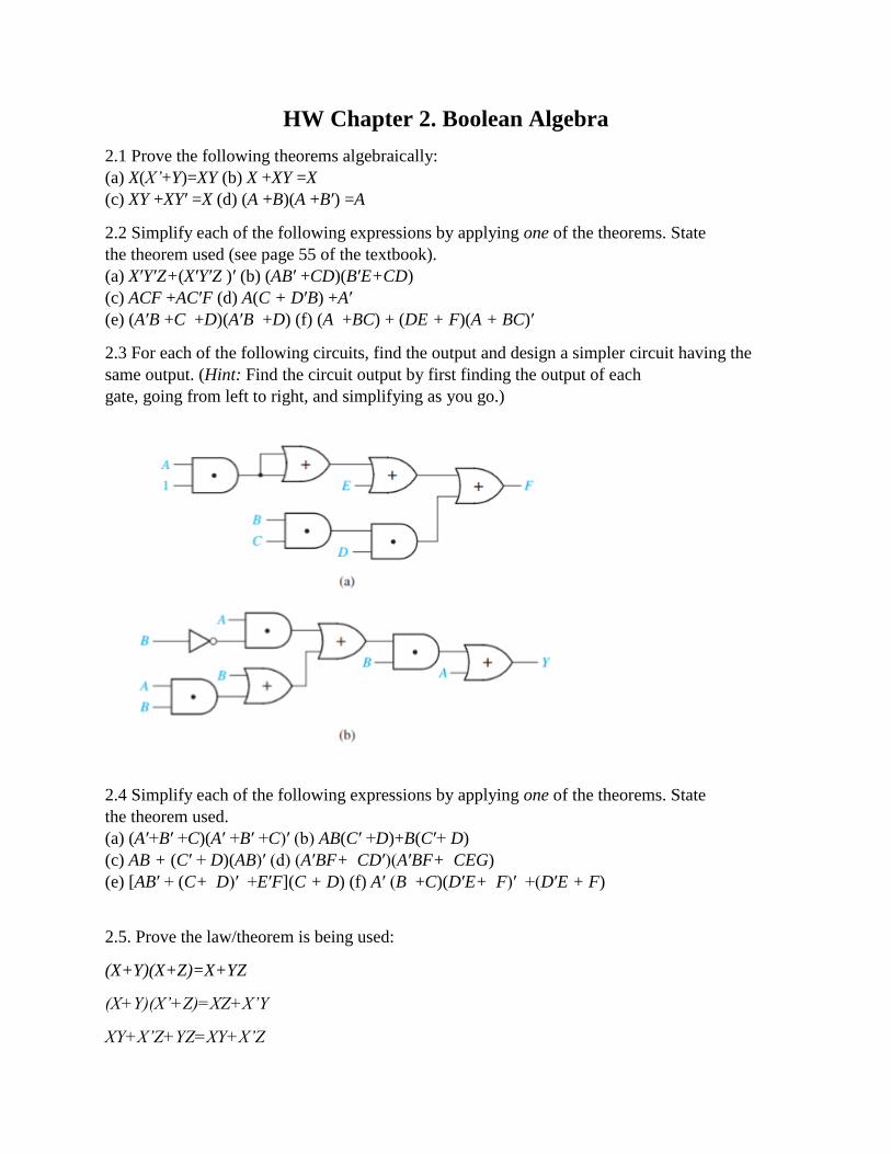
2.3 For each of the following circuits, find the output and design a simpler circuit having the
same output. (Hint: Find the circuit output by first finding the output of each
gate, going from left to right, and simplifying as you go.)
2.4 Simplify each of the following expressions by applying one of the theorems. State
the theorem used.
(a) (A′+B′ +C)(A′ +B′ +C)′ (b) AB(C′ +D)+B(C′+ D)
(c) AB + (C′ + D)(AB)′ (d) (A′BF+ CD′)(A′BF+ CEG)
(e) [AB′ + (C+ D)′ +E′F](C + D) (f) A′ (B +C)(D′E+ F)′ +(D′E + F)
2.5. Prove the law/theorem is being used:
(X+Y)(X+Z)=X+YZ
(X+Y)(X’+Z)=XZ+X’Y
XY+X’Z+YZ=XY+X’Z
2.6 Prove:
(X Y)’=XY+X’Y’
2.7 Convert the following to SOP:
A’ B C
2.8. Simplify:
QX+X’Z’+XY+QY’Z’
2.9. In each case, multiply out to obtain a sum of products: (Simplify where possible.)
(a) (W+ X’+ Z’ ) (W ’+ Y’ ) (W ’+ X+ Z’ ) (W +X’ ) (W +Y+ Z)
(b) (A +B + C +D) (A’+ B’+ C + D’ ) (A ’+C) (A+ D) (B + C+ D)
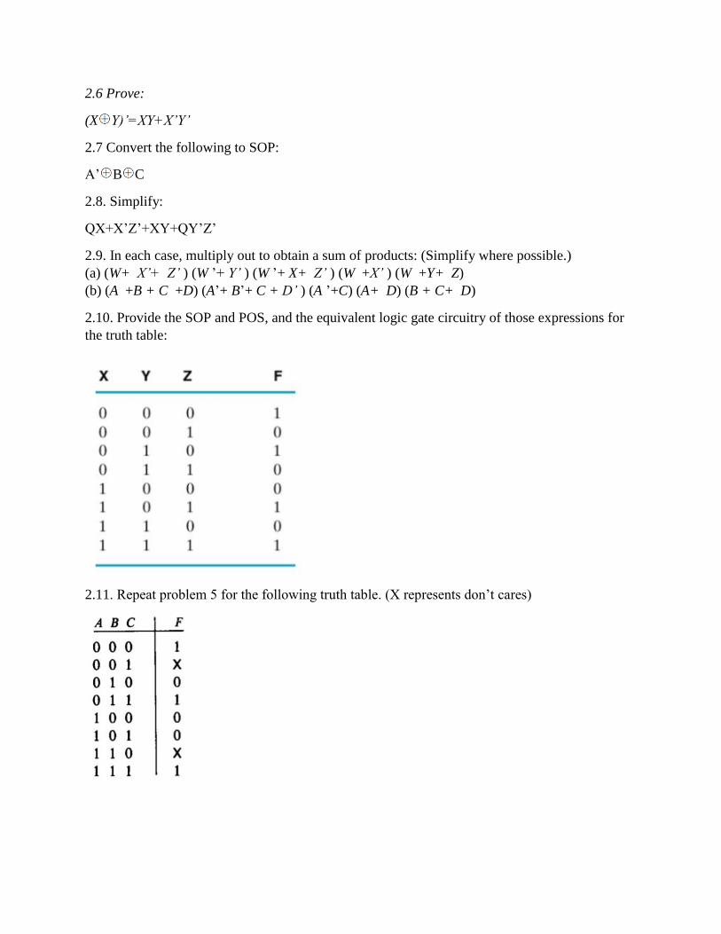
2.10. Provide the SOP and POS, and the equivalent logic gate circuitry of those expressions for
the truth table:
2.11. Repeat problem 5 for the following truth table. (X represents don’t cares)
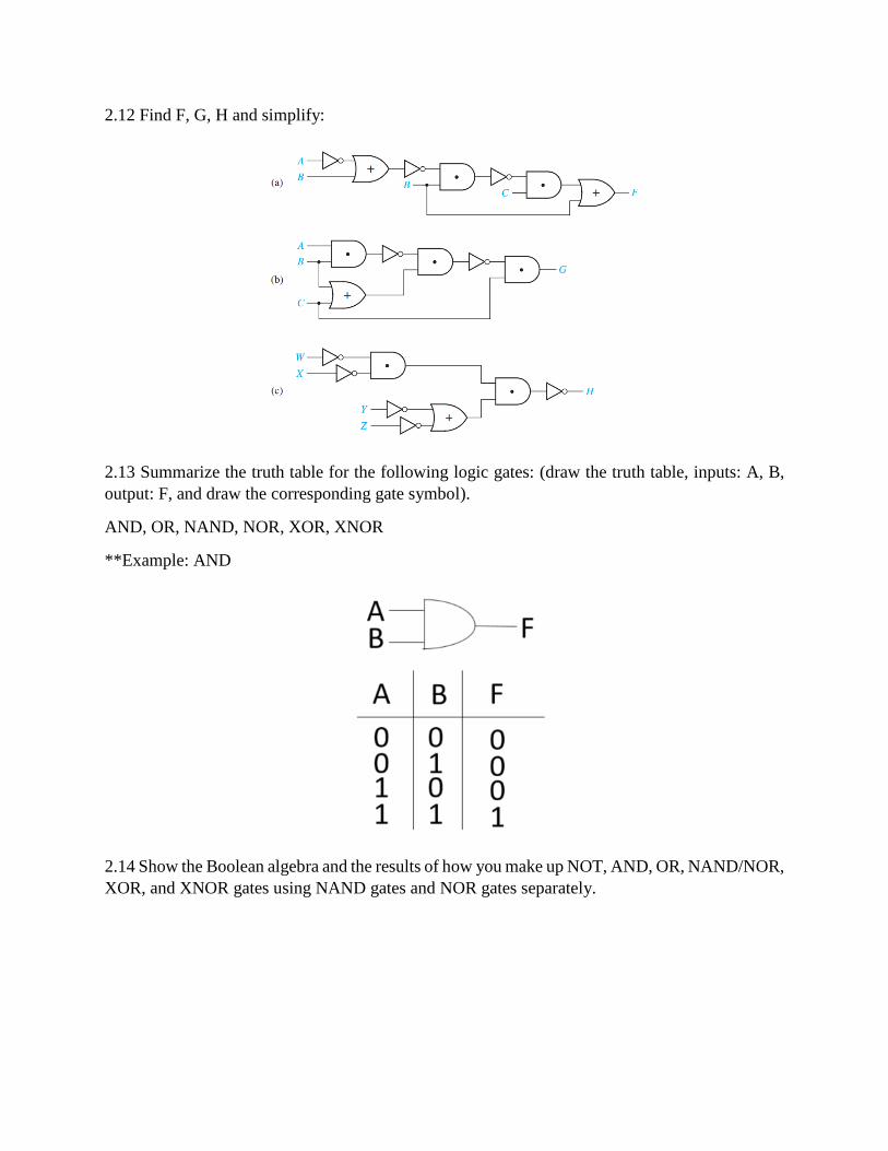
2.12 Find F, G, H and simplify:
2.13 Summarize the truth table for the following logic gates: (draw the truth table, inputs: A, B,
output: F, and draw the corresponding gate symbol).
AND, OR, NAND, NOR, XOR, XNOR
**Example: AND
2.14 Show the Boolean algebra and the results of how you make up NOT, AND, OR, NAND/NOR,
XOR, and XNOR gates using NAND gates and NOR gates separately.
HW Chapter 3. CMOS Logic
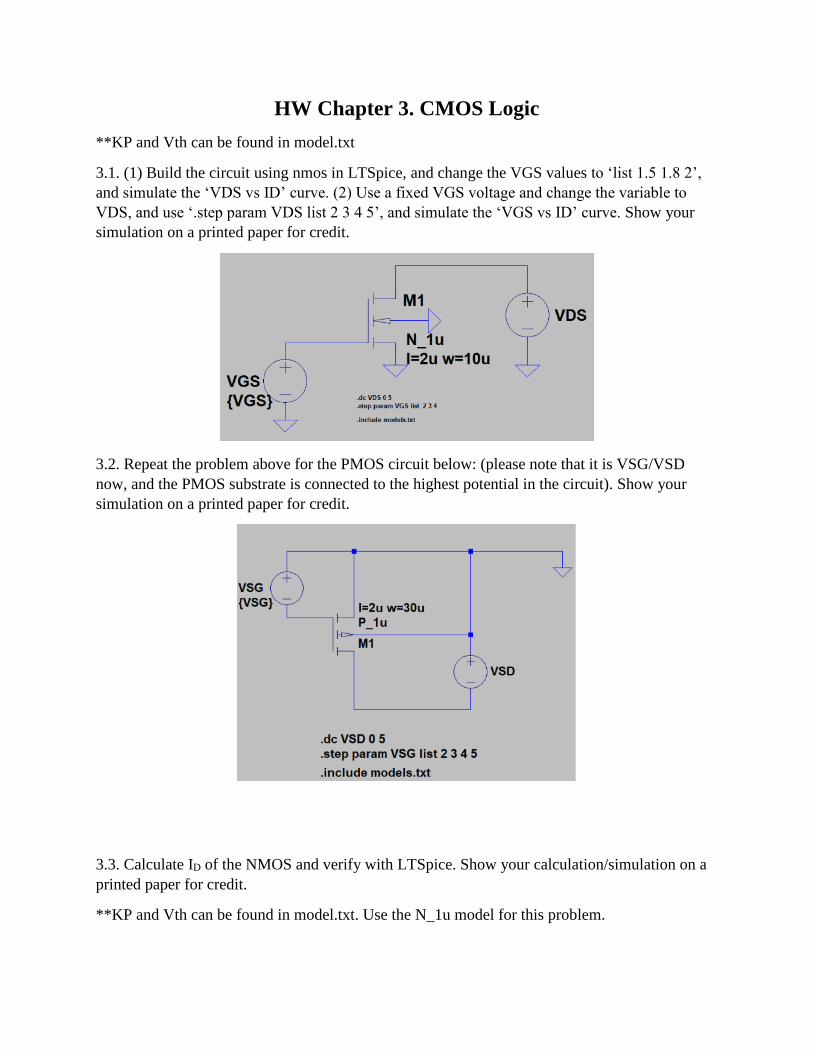
**KP and Vth can be found in model.txt
3.1. (1) Build the circuit using nmos in LTSpice, and change the VGS values to ‘list 1.5 1.8 2’,
and simulate the ‘VDS vs ID’ curve. (2) Use a fixed VGS voltage and change the variable to
VDS, and use ‘.step param VDS list 2 3 4 5’, and simulate the ‘VGS vs ID’ curve. Show your
simulation on a printed paper for credit.
3.2. Repeat the problem above for the PMOS circuit below: (please note that it is VSG/VSD
now, and the PMOS substrate is connected to the highest potential in the circuit). Show your
simulation on a printed paper for credit.
3.3. Calculate ID of the NMOS and verify with LTSpice. Show your calculation/simulation on a
printed paper for credit.
**KP and Vth can be found in model.txt. Use the N_1u model for this problem.

Fig. 3.1
3.4. Calculate ID of the PMOS and verify with LTSpice. Show your calculation/simulation on a
printed paper for credit.
**KP and Vth can be found in model.txt. Use the P_1u for this problem.
Fig. 3.2
3.5. Design an inverter use long_channel devices (N_1u, P_1u), and make a symbol out of it,
use a new schematic to put your symbol there and simulate the input vs. output voltage curve,
and mark the switching point on the curve.
3.6. Use the short-channel devices (N_50n, P_50n): (1) Build the inverter and the symbol
accordingly to the Fig. 3.3 by yourself. (2) Calculate and simulate the propagation delay: (for the
W/L shown in the Fig. 3.3, Rn=Rp=3.4 kohm, Coxn=625 aF, Coxp=1.25 fF).
a. b.
Fig. 3.3
3.7. (1) Design a ring oscillator using the inverter you designed in Problem 3.6. (2) Use this
inverter to build a ring oscillator (make it as fast as you can), and calculate and simulate the
frequency it oscillates.
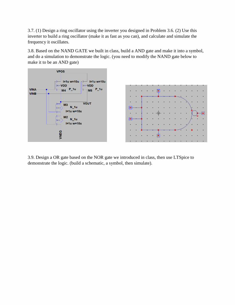
3.8. Based on the NAND GATE we built in class, build a AND gate and make it into a symbol,
and do a simulation to demonstrate the logic. (you need to modify the NAND gate below to
make it to be an AND gate)
3.9. Design a OR gate based on the NOR gate we introduced in class, then use LTSpice to
demonstrate the logic. (build a schematic, a symbol, then simulate).
HW Chapter 4. Minterms and Maxterms
4.1 Find the minimum sum of products for each function using a Karnaugh map
(1) f1(a, b, c)= m0 +m2 + m5 +m6
(2) f2(d, e, f ) = m0 +m1 + m2 +m4
(3) f3(r, s, t) = rt’+ r’s’+ r’s
(1) f4(x, y, z) = M0 • M5
4.2 (a) Plot the following function on a Karnaugh map. (Do not expand to minterm form before
plotting.)
F(A,B,C,D) =BD’+ B’CD + ABC +ABC’D + B’D’
(b) Find the minimum sum of products.
(c) Find the minimum product of sums.
4.3 Find the minimum sum-of-products expression for each function. Underline the essential
prime implicants in your answer and tell which minterm makes each one essential
(a) f(a, b, c, d )=∑ 𝑚(0, 1, 3, 5, 6, 7, 11, 12, 14)
(b) f(a, b, c, d )= ∏ 𝑀(1, 9, 11, 12, 14)
4.4 Find the minimum sum-of-products expression for each function
(a) f(a, b, c, d) =∑ 𝑚(0, 2, 3, 4, 7,8, 14)
(b) f(a, b, c, d )= ∏ 𝑀(1, 2,3, ,4,9,15)
4.5 Find the minimum sum of products for each of these functions.
(a) f1(A, B, C )= m1 + m3 +m4 +m6
(b) f2(d, e, f )= ∑ 𝑚(1, 4, 5, 7)
(c) f3(r, s, t)= r’ t’+ rs’+ rs
(d) f1(a, b, c) = m3 + m4 + m6 + m7
(e) f2(n, p, q) =∑ 𝑚(2, 3, 5, 7)
(f) f4 (x, y, z) = M3M6
4.6 Build a half-adder and a full-adder using logic gates (use CMOS transistors and make them into
symbols in LTSpice), and simulate the logic and compare the waveform with the truth tables.
4.7 Derive the logic expression of the carries and the sum of a 4-bit carry look-ahead adder and explain
why this is better than the ripple carry adder.
4.8 Use the FA in 4.6, build a 3-bit FA (ripple-carry FA), and demonstrate the following logic:
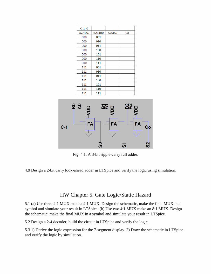
Fig. 4.1, A 3-bit ripple-carry full adder.
4.9 Design a 2-bit carry look-ahead adder in LTSpice and verify the logic using simulation.
HW Chapter 5. Gate Logic/Static Hazard
5.1 (a) Use three 2:1 MUX make a 4:1 MUX. Design the schematic, make the final MUX in a
symbol and simulate your result in LTSpice. (b) Use two 4:1 MUX make an 8:1 MUX. Design
the schematic, make the final MUX in a symbol and simulate your result in LTSpice.
5.2 Design a 2-4 decoder, build the circuit in LTSpice and verify the logic.
5.3 1) Derive the logic expression for the 7-segment display. 2) Draw the schematic in LTSpice
and verify the logic by simulation.
5.4 (a) Show how two 2-to-1 multiplexers (with no added gates) could be connected to
form a 3-to-1 MUX. Input selection should be as follows:
If AB 00, select I0
If AB 01, select I1
If AB 1– (B is a don’t-care), select I2
(b) Show how two 4-to-1 and one 2-to-1 multiplexers could be connected to form an
8-to-1 MUX with three control inputs.
(c) Show how four 2-to-1 and one 4-to-1 multiplexers could be connected to form an
8-to-1 MUX with three control inputs.
5.5. Implement a full adder using a 3-to-8 line decoder (as in Figure 9-13) and
(a) two OR gates.
(b) two NOR gates.
5.6 Show how to make a 4-to-1 MUX, using an 8-to-1 MUX.
5.7. Draw the truth table of the 4-2 encoder, and write down the logic expressions for the output.
5.8 Consider the following logic function.
F(A, B, C, D) =∑ 𝑚(0, 2, 5, 6, 7, 8, 9, 12, 13, 15)
(a) Find the minimum AND-OR circuits which implement F. Identify two
hazards in the circuit. Then find an AND-OR circuit for F that has no hazards. (AND-OR means
do AND first then OR everything together, which means the logic expression is in minterms).
(b) Find the minimum OR-AND circuit for F has hazards. Identify it, and then find
an OR-AND circuit for F that has no hazards.
5.9 Design a decoder that can control two traffic light sets in at cross street (input: A, B, C,
output: G1, Y1, R1; G2, Y2, R2). Draw the schematic in LTSpice and verify the logic.
5.10 Referring to the 4:1 MUX in the notes, design a 2:1 MUX in LTSpice and verify the logic
with simulation.

HW Chapter 6. Latches/FlipFlops
6.1. Draw the truth table and characteristic table for the SR latch (by NOR gates). Use LTSpice
to verify the logic.
6.2. Draw the truth table and characteristic table for the SR latch (by NAND gates). Use LTSpice
to verify the logic.
6.3. Draw the Characteristic Table of the SR FlipFlop, D FlipFlop, and JK FlipFlop. Verify in LTSpice.
6.4 What happens when S = R =1 for each circuit?
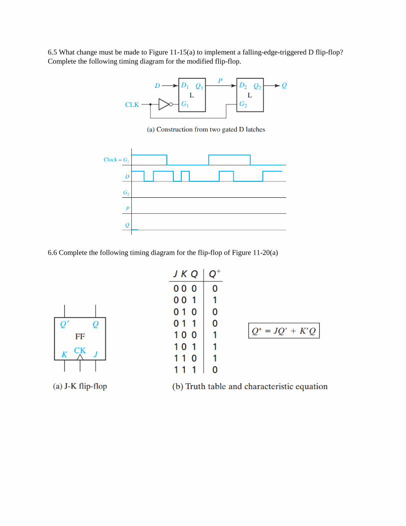
6.5 What change must be made to Figure 11-15(a) to implement a falling-edge-triggered D flip-flop?
Complete the following timing diagram for the modified flip-flop.
6.6 Complete the following timing diagram for the flip-flop of Figure 11-20(a)
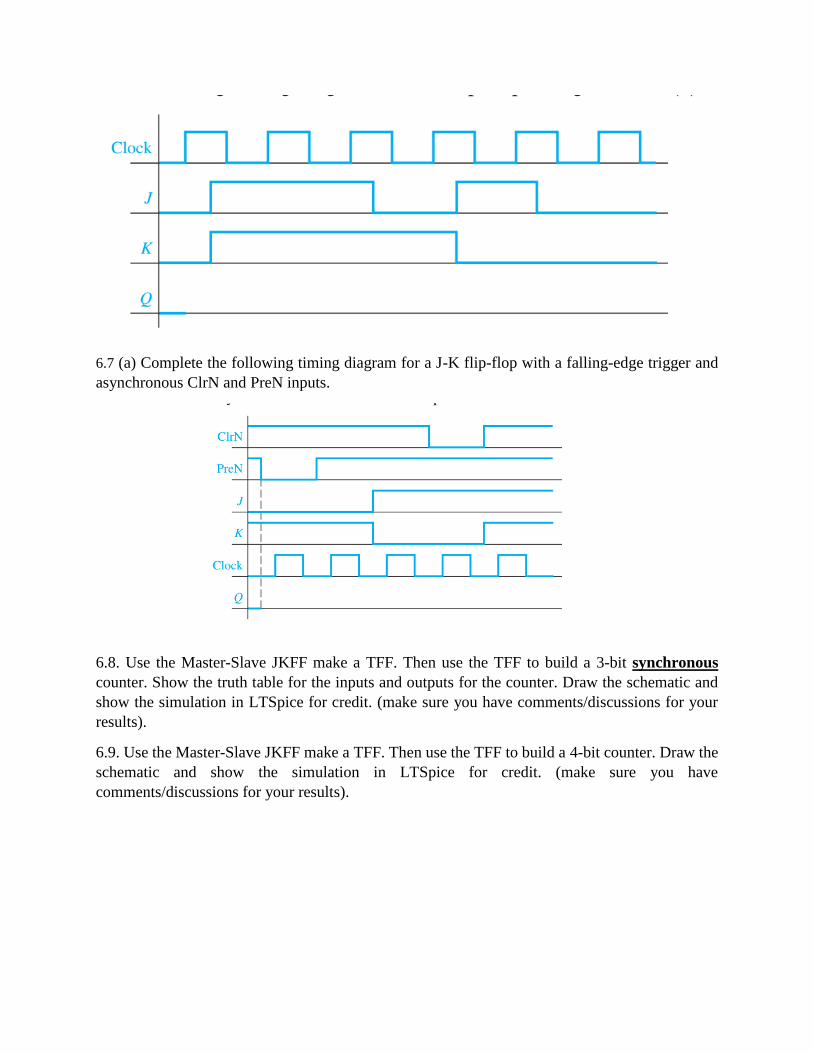
6.7 (a) Complete the following timing diagram for a J-K flip-flop with a falling-edge trigger and
asynchronous ClrN and PreN inputs.
6.8. Use the Master-Slave JKFF make a TFF. Then use the TFF to build a 3-bit synchronous
counter. Show the truth table for the inputs and outputs for the counter. Draw the schematic and
show the simulation in LTSpice for credit. (make sure you have comments/discussions for your
results).
6.9. Use the Master-Slave JKFF make a TFF. Then use the TFF to build a 4-bit counter. Draw the
schematic and show the simulation in LTSpice for credit. (make sure you have
comments/discussions for your results).
HW Chapter 7 Hardware Description Languages
7.1 Use Vivado to model the following logic gates and verify with simulations in Vivado.
1) AND 2) OR 3) XOR 4) 2:1 MUX 5) Inverter 6) A 3-bit Full Adder.
Report the code and the waveform in your homework.
7.2 Hand write (neither type in a text editor, nor in Vivado) the logic block Verilog codes, and
their corresponding test benches for the following modules:
1) A clock divider, to make an output clock signal of 10 Hz, and the output signal is showing at
the I/O pin of JB[3].
2) A module to display number ‘8’ at the first seven segment display device from the left side.
Please note that you need to disable all other 3 seven segment display devices.
3) Make your number ‘8’ from the last problem flashing in the frequency of 1 Hz.
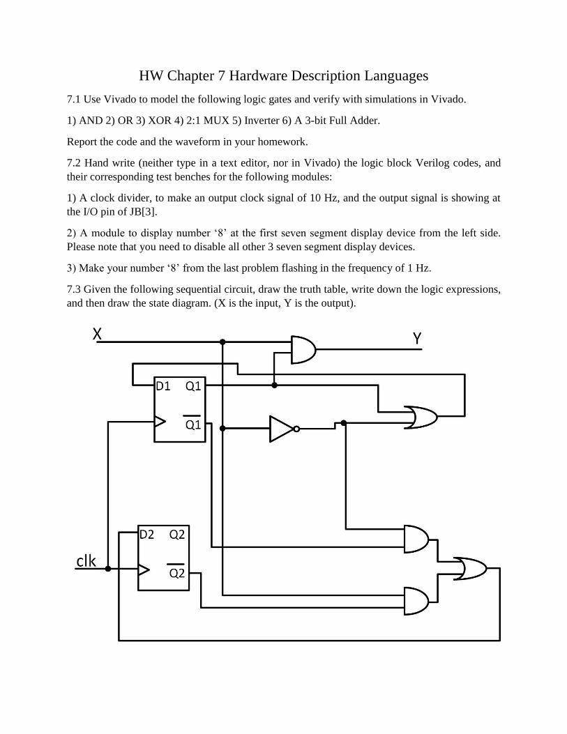
7.3 Given the following sequential circuit, draw the truth table, write down the logic expressions,
and then draw the state diagram. (X is the input, Y is the output).