section 5 high speed pcb layout techniques - ti. · pdf filethis section looks at some key...
TRANSCRIPT

High Speed Analog Design and Application Seminar
5-1Texas Instruments
Section 5
High Speed PCB Layout Techniques
Scenario: You have spent several days, no maybe weeks, perfecting adesign on paper and also using Spice to ensure the design exceeds allexpectations. You hand the schematic to your layout person who puts alleverything on a printed circuit board (PCB). The PCB comes back in a weekor two and is finally populated and ready to test. But it doesn’t work!!!!
Why not? On paper it works!! Spice said it works!! But it doesn’t work!!
This scenario happens more often than not and the reason many circuits donot work as expected is due primarily to the PCB layout.
This section looks at some key fundamentals of high speed PCB layouttechniques so that hopefully the above scenario will never happen to you.
High Speed Analog Design and Application Seminar
5-2Texas Instruments
PCB Components
⎟⎠⎞
⎜⎝⎛
+≈
twhlnL(nH)
0.85.982x
( )
0.85.98
1.410.264x
⎟⎠⎞
⎜⎝⎛
+
+≈
twhln
rC(pF) εht
wεr
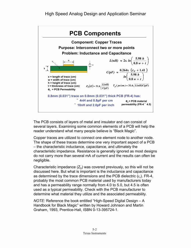
Component: Copper TracesPurpose: Interconnect two or more points
Problem: Inductance and Capacitance
x = length of trace (cm)w = width of trace (cm)h = height of trace (cm)t = thickness of trace (cm)er = PCB Permeability
0.8mm (0.031”) trace on 0.8mm (0.031”) thick PCB (FR-4) has: ˜ 4nH and 0.8pF per cm
˜ 10nH and 2.0pF per inch
L(nH)C(pF))ps/cm(Tp 31.6=( )C(pF)L(nH)Z0 31.6=Ω
er = PCB materialpermeability (FR-4 ˜ 4.5)
The PCB consists of layers of metal and insulator and can consist ofseveral layers. Examining some common elements of a PCB will help thereader understand what many people believe is “Black Magic”.
Copper traces are utilized to connect one element node to another node.The shape of these traces determine one very important aspect of a PCB– the characteristic inductance, capacitance, and ultimately thecharacteristic impedance. Resistance is generally ignored as most designsdo not carry more than several mA of current and the results can often benegligible.
Characteristic impedance (Z0) was covered previously, so this will not bediscussed here. But what is important is the inductance and capacitanceas determined by the trace dimensions and the PCB dielectric (εr). FR-4,probably the most common PCB material used by manufacturers todayand has a permeability range normally from 4.0 to 5.0, but 4.5 is oftenused as a typical permeability. Check with the PCB manufacturer todetermine what material they utilize and the associated permeability.
NOTE: Reference the book entitled “High-Speed Digital Design – AHandbook for Black Magic” written by Howard Johnson and MartinGraham, 1993, Prentice-Hall, ISBN 0-13-395724-1.

High Speed Analog Design and Application Seminar
5-3Texas Instruments
0.0886h
C(pF) A rε≈
Component: Copper PlanesPurpose: Used For Ground Planes and Power Planes
Problem: Stray Capacitance on Signal TracesBenefit: Large Bypass Capacitance & Minimal Inductance
h = separation between planes (cm)A = area of common planes = l*w (cm2)er = PCB Permeability
0.8mm (0.031”) thick PCB (FR-4) has: ˜ 0.5pF per cm2
˜ 32.7pF per inch2
h εr
w
l A
er = PCB materialpermeability (FR-4 ˜ 4.5)
PCB Components
Copper planes are typically found when power planes and ground planesare utilized. Planes make an excellent high frequency capacitor and canoften be utilized for high frequency bypassing in complement withtraditional capacitors.
The use of a solid ground plane is generally preferred over a grid plane. Asolid plane minimizes inductance to the absolute minimum which is adesirable trait for high speed signals – which includes both Analog andDigital signals. But, as will be discussed later, this plane can causecapacitance problems to sensitive nodes of the circuit. Be aware of allattributes of the circuit and do not blindly use planes everywhere.
A side benefit of a solid plane is it becomes a very good thermal conductorand can act as a heat sink to keep thermal levels of all devices minimized.But on the flip side, temperature sensitive components may not want tohave the ground plane nearby due to this heat spreading.

High Speed Analog Design and Application Seminar
5-4Texas Instruments
0.4mm (0.0157”) via with 1.6mm (0.063”) thick PCB has ˜ 1.2nH1.6mm (0.063”) Clearance hole around 0.8mm (0.031”) pad on FR-4 has ˜ 0.4pF
Component: ViasPurpose: Interconnect traces on different layers
Problem: Inductance and Capacitance
PCB Components
⎥⎦
⎤⎢⎣
⎡⎟⎠⎞
⎜⎝⎛+≈
dhlnhL(nH) 41
5
12
1 05550dd
d h C(pF) r−
≈ε.
er = PCB material permeability (FR-4 ˜ 4.5)
L(nH)C(pF))ps/cm(Tp 31.6=( )C(pF)L(nH)Z0 31.6=Ω
Vias are utilized to simplify trace routing around other components or whenthere is a high density of interconnections to be made (i.e. BGApackages). Just as a PCB trace had inductance and capacitance, so todoes a via. Generally these elements are ignored as the length of the viasare typically very small relative to the rest of the trace. But, this Can causeissues if the signals are very high frequency (>100MHz) or have energy /harmonics at high frequencies.
The easiest way to minimize problems of a via is to simply not use themwith signal traces. At the very least it should be minimized. If vias must beused, there are other issues to worry about that will be discussed later.

High Speed Analog Design and Application Seminar
5-5Texas Instruments
ht
wεr
D
21
⎟⎠⎞
⎜⎝⎛+
×=
hD1
h Ii(A/cm) Oπ
i(A/cm)IO = total signal current (A)h = height of trace (cm)D = distance from trace (cm)
Current Density
Illustrates Return Current Flow is directly below thesignal trace. The creates the path of least impedance.Must have Solid return path (i.e. Solid Ground Plane)under the signal trace to maintain homogeneous natureof current density.
Current density is the concentration of current flowing through a conductor.This is especially important when looking at return currents.
One thing that many people forget about is for a current to flow out to apoint, there MUST be a return path or else current will Not flow. Sincethere is a current flow, then the return current flow will find a way back toits’ source one way or another. Return current density is highest directlyunder (or over) the signal trace it was sourced from. Even if a solid groundplane is used, the concentration of current flow will still be adjacent to thesignal source trace.
High Speed Analog Design and Application Seminar
5-6Texas Instruments
High Frequency Input Current Path
RTERMVia to Bottom
GND Plane
Via
Top LayerCurrent Flow
Botttom LayerCurrent Flow
RTERMVia to Bottom
GND Plane
Via
RTERMVia to BottomGND Plane
Via
Break in GNDPlane
Picks upHF Return
ThruReference
+-
NOISE
BADLarge
Current Loop
BETTERReduced
Current Loop
BESTMinimum Current
Loop
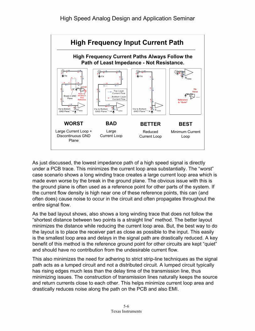
High Frequency Current Paths Always Follow thePath of Least Impedance - Not Resistance.
WORSTLarge Current Loop +Discontinuous GND
Plane
RTERM
+-
NoNoise
Referenceis “Quiet”
As just discussed, the lowest impedance path of a high speed signal is directlyunder a PCB trace. This minimizes the current loop area substantially. The “worst”case scenario shows a long winding trace creates a large current loop area which ismade even worse by the break in the ground plane. The obvious issue with this isthe ground plane is often used as a reference point for other parts of the system. Ifthe current flow density is high near one of these reference points, this can (andoften does) cause noise to occur in the circuit and often propagates throughout theentire signal flow.
As the bad layout shows, also shows a long winding trace that does not follow the“shortest distance between two points is a straight line” method. The better layoutminimizes the distance while reducing the current loop area. But, the best way to dothe layout is to place the receiver part as close as possible to the input. This easilyis the smallest loop area and delays in the signal path are drastically reduced. A keybenefit of this method is the reference ground point for other circuits are kept “quiet”and should have no contribution from the undesirable current flow.
This also minimizes the need for adhering to strict strip-line techniques as the signalpath acts as a lumped circuit and not a distributed circuit. A lumped circuit typicallyhas rising edges much less than the delay time of the transmission line, thusminimizing issues. The construction of transmission lines naturally keeps the sourceand return currents close to each other. This helps minimize current loop area anddrastically reduces noise along the path on the PCB and also EMI.
High Speed Analog Design and Application Seminar
5-7Texas Instruments
RSOURCE
+VS
-VS
High Frequency Output Current Path
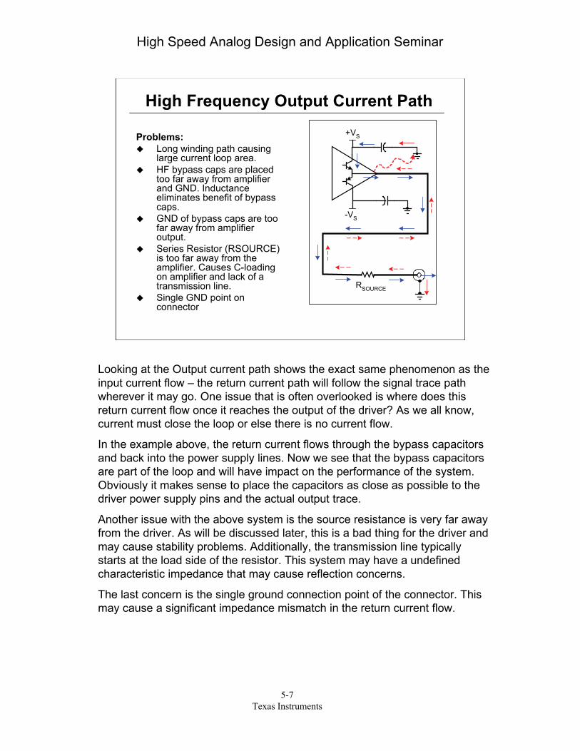
Problems:Long winding path causinglarge current loop area.HF bypass caps are placedtoo far away from amplifierand GND. Inductanceeliminates benefit of bypasscaps.GND of bypass caps are toofar away from amplifieroutput.Series Resistor (RSOURCE)is too far away from theamplifier. Causes C-loadingon amplifier and lack of atransmission line.Single GND point onconnector
Looking at the Output current path shows the exact same phenomenon as theinput current flow – the return current path will follow the signal trace pathwherever it may go. One issue that is often overlooked is where does thisreturn current flow once it reaches the output of the driver? As we all know,current must close the loop or else there is no current flow.
In the example above, the return current flows through the bypass capacitorsand back into the power supply lines. Now we see that the bypass capacitorsare part of the loop and will have impact on the performance of the system.Obviously it makes sense to place the capacitors as close as possible to thedriver power supply pins and the actual output trace.
Another issue with the above system is the source resistance is very far awayfrom the driver. As will be discussed later, this is a bad thing for the driver andmay cause stability problems. Additionally, the transmission line typicallystarts at the load side of the resistor. This system may have a undefinedcharacteristic impedance that may cause reflection concerns.
The last concern is the single ground connection point of the connector. Thismay cause a significant impedance mismatch in the return current flow.

High Speed Analog Design and Application Seminar
5-8Texas Instruments
High Frequency Output Current Path
Solutions:Amplifier is next to Connectorminimizing loop area.HF bypass caps are nowplaced next to amplifierpower supply pins and hasshort GND connection.GND of bypass caps nearamplifier output – but not tooclose to cause C-loadingissues.Source Resistance is next toamplifier output.Multiple GND points onconnector.
RSOURCE
+VS
-VS
As seen before, the simple solution is to simply minimize the current flowarea as much as possible. Easily solved by moving the connector and thedriver next to each other. The bypass caps are now very close to the driverpower supply pins and have very short trace lengths that are near thedriver output pin. The series resistor that matches the transmission linecharacteristic impedance is placed very close to the driver. Additionally theconnector has multiple ground connection points to minimize impedanceissues.

High Speed Analog Design and Application Seminar
5-9Texas Instruments
RS
+VS
-VS
+VS
-VS
1:N
RSN2
RSN2
High Frequency Output Current Path DifferentiallyFrom 2 Amplifiers
Minimize Loop Area on DriverSide.Utilize a single Capacitorbetween opposite amplifiersupplies as this should be themain current flow. Adding thisCapacitor can reduce 2nd-Order Distortion by 6 to 10dB!Use bypass caps to GND at amid-point to handle stray-Creturn path currents but do notdisrupt differential current flow.
Using two individual amplifiers in a differential drive configuration, such asa ADSL line driver, also must follow the same concepts discussedpreviously. The use of a transformer helps isolate the driver-side currentflow and the line side current flow. Since the drivers’ outputs aredifferential, there must be a differential current flow from one driver to theother. The bypass capacitors allow this to occur and should follow theconcepts previously discussed. The only difference here is we want toforce the current to flow through a bypass capacitor connected from thepositive supply of one driver to the negative supply of the other driver.
The use of bypass capacitors to the ground plane will still be required, aswill be discussed later. To make sure the current does NOT flow into theground, place these capacitors symmetrically to each other and connectthe ground at the midpoint of the capacitors. The differential current flowshould have no reason to go into the ground plane. Combined with thesingle capacitor across the supplies, this configuration can reduce even-order harmonics by 6 to 12dB.
Although not shown above, there will be interwinding capacitance acrossthe transformer windings. There must be a way for high frequency currentflowing through this capacitance to return back to the source, or else therecan be issues.

High Speed Analog Design and Application Seminar
5-10Texas Instruments
+VS
-VS
Fully DifferentialAmplifier
(ex. THS4502)ADC
(ex. ADS5500)
High Frequency Output Current Path DifferentiallyFrom Fully Diff. Amplifier
Minimize Loop Areaon Driver Side.Utilize a singleCapacitor betweenopposite amplifiersupplies as this shouldbe the main currentflow.Use bypass caps toGND at a mid-point tohandle stray-C returnpath currents but donot disrupt differentialcurrent flow.Filter Cap should allowfor small Loop Areas –including “kick-back”current flow.
A fully differential amplifier follows essentially the same concepts as thesingle-ended differential driver. The only difference is the two outputs arein the same package. But, the bypass capacitors should follow the sameprinciples as mentioned before – one capacitor form the positive supply tothe negative supple, and the two bypass capacitors to ground shouldoptimally be placed symmetrically to each other and connected to groundat the midpoint.
One of the most common uses for a fully differential amplifier is to drive anADC. When doing this, pay attention to the current flows around theamplifier and the ADC (caused by the ADC’s internal capacitor). Keep thepaths as symmetrical as possible.

High Speed Analog Design and Application Seminar
5-11Texas Instruments
+VS
-VS
Fully DifferentialAmplifier
(ex. THS4502)ADC
(ex. ADS5500)
StrayCapacitance
Remember: Minimize ALL Current Loops – Differential AND Common-Mode
Why Add Bypass Capacitors to Ground?
Allows Common-ModeReturn Currents a pathback to the source tocomplete the loop.
Hopefully, does NOTdisrupt DifferentialCurrent Flow – hence themid-point grounding.
Some of these currentswill flow back into theopposite phased signalpath through the straycapacitance.
Adding capacitors to ground, even in a fully differential system, needs tobe done to account for the current flowing through the stray capacitance ofthe system. This stray capacitance can even occur inside the silicon of thedriver and/or the ADC. As you know by now, the current will find a wayback to its’ source in-order to complete the loop. The bypass capacitors toground allow this current flow to occur and will minimize the loop area.

High Speed Analog Design and Application Seminar
5-12Texas Instruments
Routing Differential Traces
Keep Differential Traces Close Together. Keeps noise injection as aCommon-Mode Signal which is attenuated in the Differential System.Route Differential Traces Around Obstacles Together, Do NotSeparate.Try to keep trace lengths the exact same length to keep delays equal.
When routing differential traces, they should always be routed together(side-by-side). This keeps any noise injection into the signal a truecommon-mode noise which gets rejected by the receiver. If noise only getsinto one channel and not the other, the amount of rejection is minimal atbest.
Additionally, the lengths of both traces should be kept the same length.Otherwise the signals can arrive at the receiver at different times andcause performance issues. This is especially true for very fast switchingdigital signals and very high analog signals (>1-GHz).

High Speed Analog Design and Application Seminar
5-13Texas Instruments
⎟⎟
⎠
⎞
⎜⎜
⎝
⎛−∗≈
−h
0.96d
0diff 0.48e1Z2)(Z Ω
( )⎟⎠⎞
⎜⎝
⎛++
≈t0.8w0.67
h4 ln 0.670.475
60)(Zr
0 εΩ
⎟⎟
⎠
⎞
⎜⎜
⎝
⎛−∗≈
−B
2.9d
0diff 0.347e1Z2)(Z Ω
( )⎟⎠⎞
⎜⎝
⎛+
≈10.8w0.67
h4 ln 60)(Zr
0 ε πΩ
ht
wεr
d w
d<w
B
εr
th
w d w
d<w
Differential TracesMICROSTRIP
Most Commonly UsedLess Propagation DelayMay Radiate more RFOnly requires 2 Layers
STRIPLINEMore Propagation DelayBetter Noise Immunity/RadiationRequires at least 3 LayersMay be harder to control Z0
Just like single traces, differential traces also can have a characteristicimpedance dictated by the inductance and capacitance. Keeping thedifferential traces close together is highly desirable as it minimizes noiseinjection problems and minimizes the radiated electromagnetic field.
High Speed Analog Design and Application Seminar
5-14Texas Instruments
w d >2w>2w
X
wd<w
Differential Traces
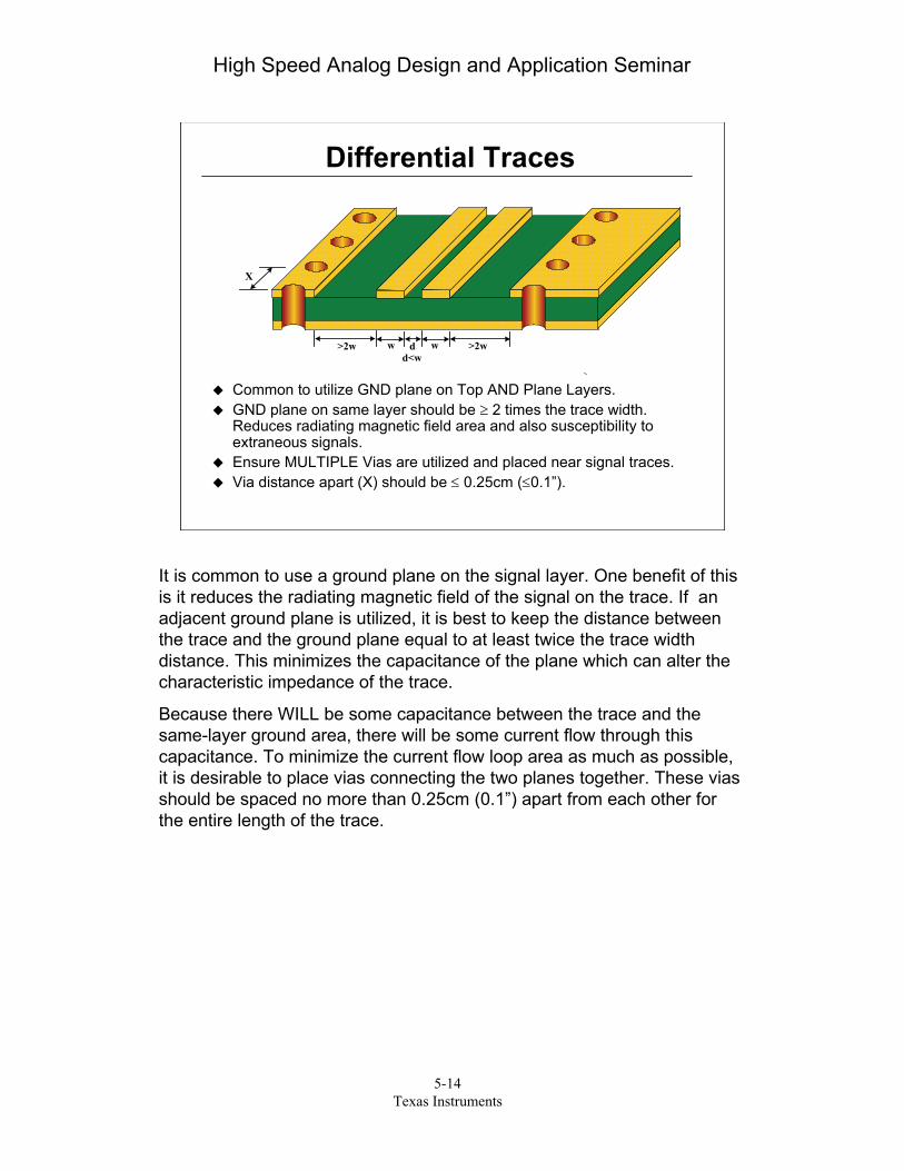
Common to utilize GND plane on Top AND Plane Layers.GND plane on same layer should be ≥ 2 times the trace width.Reduces radiating magnetic field area and also susceptibility toextraneous signals.Ensure MULTIPLE Vias are utilized and placed near signal traces.Via distance apart (X) should be ≤ 0.25cm (≤0.1”).
It is common to use a ground plane on the signal layer. One benefit of thisis it reduces the radiating magnetic field of the signal on the trace. If anadjacent ground plane is utilized, it is best to keep the distance betweenthe trace and the ground plane equal to at least twice the trace widthdistance. This minimizes the capacitance of the plane which can alter thecharacteristic impedance of the trace.
Because there WILL be some capacitance between the trace and thesame-layer ground area, there will be some current flow through thiscapacitance. To minimize the current flow loop area as much as possible,it is desirable to place vias connecting the two planes together. These viasshould be spaced no more than 0.25cm (0.1”) apart from each other forthe entire length of the trace.
High Speed Analog Design and Application Seminar
5-15Texas Instruments
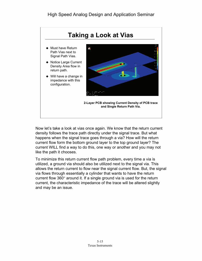
2-Layer PCB showing Current Density of PCB traceand Single Return Path Via.
Taking a Look at Vias
Must have ReturnPath Vias next toSignal Path Vias.
Notice Large CurrentDensity Area flow inreturn path.
Will have a change inimpedance with thisconfiguration.
Now let’s take a look at vias once again. We know that the return currentdensity follows the trace path directly under the signal trace. But whathappens when the signal trace goes through a via? How will the returncurrent flow form the bottom ground layer to the top ground layer? Thecurrent WILL find a way to do this, one way or another and you may notlike the path it chooses.
To minimize this return current flow path problem, every time a via isutilized, a ground via should also be utilized next to the signal via. Thisallows the return current to flow near the signal current flow. But, the signalvia flows through essentially a cylinder that wants to have the returncurrent flow 360° around it. If a single ground via is used for the returncurrent, the characteristic impedance of the trace will be altered slightlyand may be an issue.
High Speed Analog Design and Application Seminar
5-16Texas Instruments
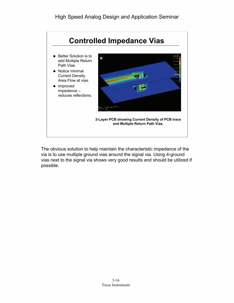
2-Layer PCB showing Current Density of PCB traceand Multiple Return Path Vias.
Controlled Impedance Vias
Better Solution is toadd Multiple ReturnPath Vias.Notice minimalCurrent DensityArea Flow at vias.Improvedimpedance –reduces reflections.
The obvious solution to help maintain the characteristic impedance of thevia is to use multiple ground vias around the signal via. Using 4-groundvias next to the signal via shows very good results and should be utilized ifpossible.

High Speed Analog Design and Application Seminar
5-17Texas Instruments
S21
-10
-9
-8
-7
-6
-5
-4
-3
-2
-1
0
0 2 4 6 8 10 12 14
Frequency [GHz]
Atte
nuat
ion
[dB
]
Single Via
Mutliple Via
3.125-Gbps PBRSEye Pattern on 2.8”(7.1cm) PCB trace
S21Results
TDRPulse
Green = Multiple ViasYellow = 1 Via
Green = Multiple ViasYellow = 1 Via
SMAConnector
SMAConnector
w/50WTerm.
Via(s)
Note Faster Rise Timew/Multiple Vias
Controlled Impedance Vias
These graphs show the difference between a single ground via and the 4-ground via configuration. These tests are real results form a test PCBconstructed to illustrate the differences between the two scenarios.
As these results show, using the 4-via configuration widens the PBRS(pseudorandom-bit-stream) eye pattern indicating a better high frequencysystem. It also improves the S21 (input reflection) considerably, and aTDR (time-domain-reflectometry) pulse shows improved impedancematching through the via.
For more information see the October 2, 2003 article in EDN magazineentitled “Designing Controlled-Impedance Vias” written by Thomas Neu,Texas Instruments.

High Speed Analog Design and Application Seminar
5-18Texas Instruments
C ESR ESL C
ESR ESL CNOM
(Temp,Freq,
Voltage)
(Temp,Voltage)RLEAK
(Voltage)
CPAR.RPAR.
( ) 2CESL
2 )X(X(ESR)Z ++=Ω
( ) L f 2X ESL πΩ =
( )C f 2
1XC πΩ =
Ideal Model Better ModelBest Model
Impedance Vs. Frequency
0.01
0.10
1.00
10.00
1 10 100 1000
Frequency - MHz
Impe
danc
e - O
hms
Z = 2 Pi f L
Z = 1 / 2 Pi f C
L = 1nHC = 0.01uF
Ideal CapacitorESL Limitation
Real Capacitor
LC21fRES π
=
Passive Component Models - Capacitors
Capacitors are utilized extensively within most systems. They are used for power-supplybypassing, AC-coupling, integrators, filtering, etc. But, capacitors are not perfectcomponents. They have elements within them that limit their usefulness. The mostpronounced elements are the true capacitance, the equivalent series resistance (ESR), andthe equivalent series inductance (ESL). It is the ESL which causes the capacitor to stopbehaving like a true capacitor at high frequencies as the impedance starts to increase ratherthan keep decreasing.
This ESL gets compounded when leaded capacitors are utilized rather than surface mounttechnology (SMT) capacitors. As the lead inductance increases, the high frequencyimpedance limitation also increases. This increase is directly proportional to the amount oflead inductance increase. For example, if the lead inductance of the example aboveincreased from 1nH to 4nH by using a leaded ceramic capacitor, the impedance due to ESLincreases by a factor of 4. The resonant frequency is also reduced by the square root of theincrease, or by a factor of 2 for this example from 50MHz to 25MHz. It should be pretty clearthat avoiding the use of any leaded device should be adhered to for high frequency designs.
It should also be noted that when multiple capacitors are placed in parallel, resonances canoccur which cause a relatively high impedance to occur. If these resonances occur at thesignal frequency or clock frequency, the effect of the capacitor is essentially nullified due tothe high impedance at this resonant frequency. Sometimes adding a resistor in seriesshould be done with one of the capacitors to dampen the resonance effect. Additionally, ithas been found that sometimes simply removing one of the parallel capacitors actually canimprove the system as the resonance is eliminated.
High Speed Analog Design and Application Seminar
5-19Texas Instruments
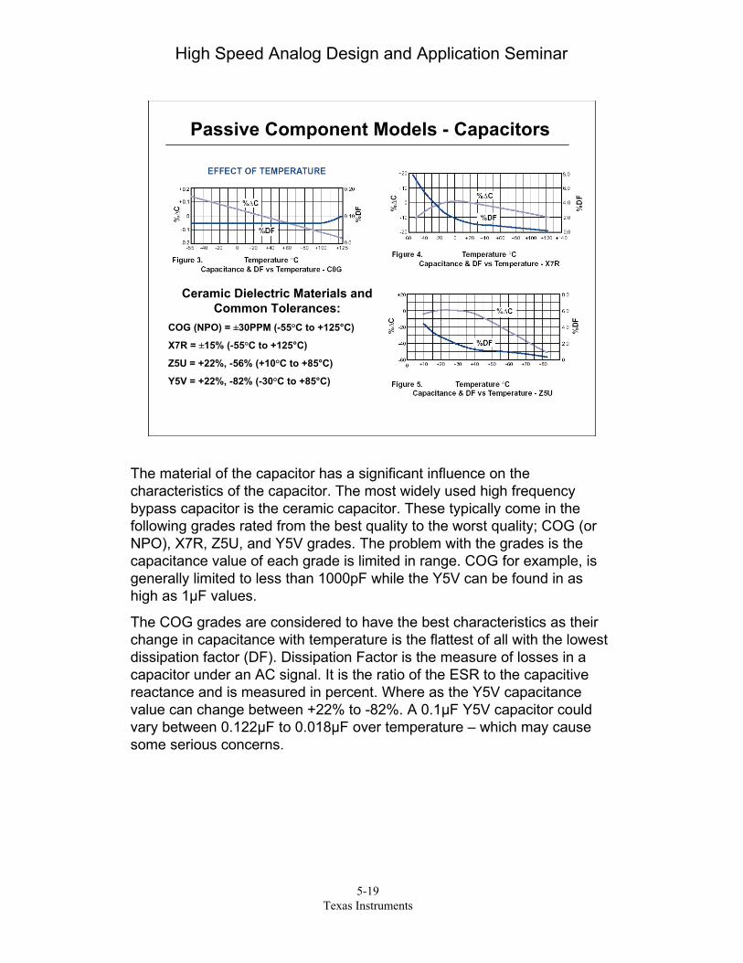
Ceramic Dielectric Materials andCommon Tolerances:
COG (NPO) = ±30PPM (-55°C to +125°C)
X7R = ±15% (-55°C to +125°C)
Z5U = +22%, -56% (+10°C to +85°C)
Y5V = +22%, -82% (-30°C to +85°C)
Passive Component Models - Capacitors
The material of the capacitor has a significant influence on thecharacteristics of the capacitor. The most widely used high frequencybypass capacitor is the ceramic capacitor. These typically come in thefollowing grades rated from the best quality to the worst quality; COG (orNPO), X7R, Z5U, and Y5V grades. The problem with the grades is thecapacitance value of each grade is limited in range. COG for example, isgenerally limited to less than 1000pF while the Y5V can be found in ashigh as 1μF values.
The COG grades are considered to have the best characteristics as theirchange in capacitance with temperature is the flattest of all with the lowestdissipation factor (DF). Dissipation Factor is the measure of losses in acapacitor under an AC signal. It is the ratio of the ESR to the capacitivereactance and is measured in percent. Where as the Y5V capacitancevalue can change between +22% to -82%. A 0.1μF Y5V capacitor couldvary between 0.122μF to 0.018μF over temperature – which may causesome serious concerns.
High Speed Analog Design and Application Seminar
5-20Texas Instruments
Passive Component Models - Capacitors
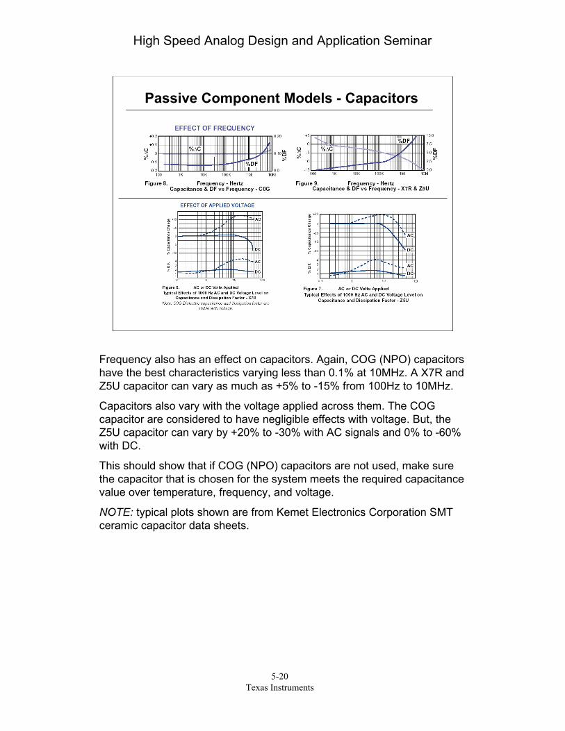
Frequency also has an effect on capacitors. Again, COG (NPO) capacitorshave the best characteristics varying less than 0.1% at 10MHz. A X7R andZ5U capacitor can vary as much as +5% to -15% from 100Hz to 10MHz.
Capacitors also vary with the voltage applied across them. The COGcapacitor are considered to have negligible effects with voltage. But, theZ5U capacitor can vary by +20% to -30% with AC signals and 0% to -60%with DC.
This should show that if COG (NPO) capacitors are not used, make surethe capacitor that is chosen for the system meets the required capacitancevalue over temperature, frequency, and voltage.
NOTE: typical plots shown are from Kemet Electronics Corporation SMTceramic capacitor data sheets.
High Speed Analog Design and Application Seminar
5-21Texas Instruments
L
DCR L
IWC
DCR L
IWCR
R
(Freq,Temp) RPAR
(Temp)
Ideal Model Better Model Best Model
( ) IWCL
IWCLXX
X XDCRZ+
+=Ω
( ) L f 2X L πΩ =
( )C f 2
1X IWC πΩ =
LC21fRES π
=
Impedance Vs. Frequency
10
100
1000
10000
1 10 100 1000
Frequency - MHz
Impe
danc
e - O
hms
Z = 2 Pi f LZ = 1 / 2 Pi f C
L = 1uHIWC = 10pF
IWC LimitationIdeal Inductor
Real Inductor
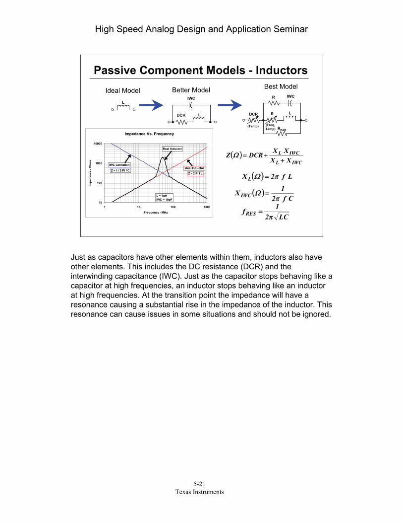
Passive Component Models - Inductors
Just as capacitors have other elements within them, inductors also haveother elements. This includes the DC resistance (DCR) and theinterwinding capacitance (IWC). Just as the capacitor stops behaving like acapacitor at high frequencies, an inductor stops behaving like an inductorat high frequencies. At the transition point the impedance will have aresonance causing a substantial rise in the impedance of the inductor. Thisresonance can cause issues in some situations and should not be ignored.

High Speed Analog Design and Application Seminar
5-22Texas Instruments
R
R LLEAD
CPackage
R LLEAD
CPackage
(Temp)
Ideal Model Better Model Best Model
Passive Component Models - Resistors
Using SMT resistors minimizes lead inductance to the point that PCB tracesare the limiting factor.
SMT packages also minimize the capacitance between the leads such thatthis parasitic is usually insignificant.
Note that resistor packs CAN have significant lead inductance and resistor-to-resistor capacitance, so choose wisely based on the application.
Resistors will have temperature coefficients, 200PPM is common, buthigher precision is available.
AVOID Wire-wound resistors and leaded resistors for high speedapplications due to their large inductance.
Resistors also have elements which make them have a frequencydependence characteristic. The capacitance is usually caused by theresistor package and the PCB mounting pads. The inductance is causedby the resistor leads and the PCB trace length.
In general, these extra elements can be ignored if the resistance value isrelatively low – below 1k-ohm for example. But, they cannot be ignored ifleaded resistors or wire wound resistors are utilized.
High Speed Analog Design and Application Seminar
5-23Texas Instruments
Poor Bypassing
Good Bypassing
Bypass Capacitors
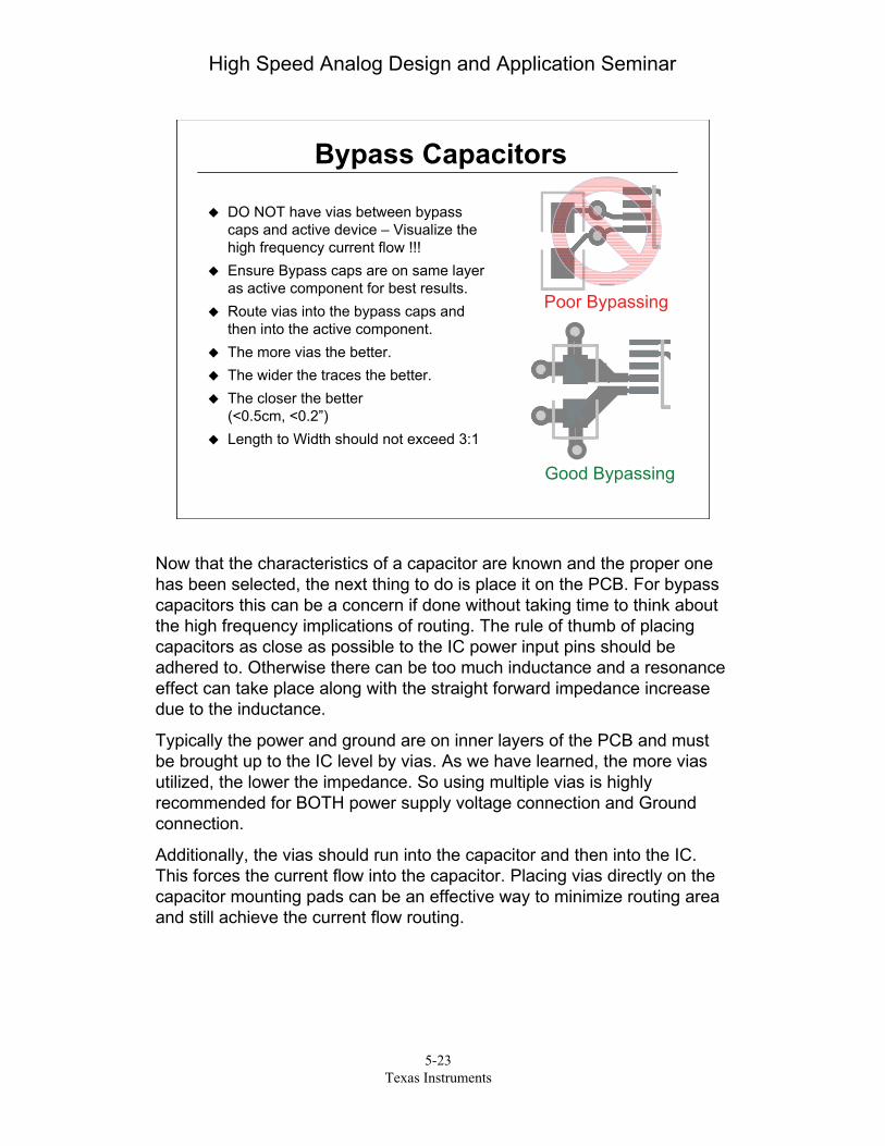
DO NOT have vias between bypasscaps and active device – Visualize thehigh frequency current flow !!!Ensure Bypass caps are on same layeras active component for best results.Route vias into the bypass caps andthen into the active component.The more vias the better.The wider the traces the better.The closer the better(<0.5cm, <0.2”)Length to Width should not exceed 3:1
Now that the characteristics of a capacitor are known and the proper onehas been selected, the next thing to do is place it on the PCB. For bypasscapacitors this can be a concern if done without taking time to think aboutthe high frequency implications of routing. The rule of thumb of placingcapacitors as close as possible to the IC power input pins should beadhered to. Otherwise there can be too much inductance and a resonanceeffect can take place along with the straight forward impedance increasedue to the inductance.
Typically the power and ground are on inner layers of the PCB and mustbe brought up to the IC level by vias. As we have learned, the more viasutilized, the lower the impedance. So using multiple vias is highlyrecommended for BOTH power supply voltage connection and Groundconnection.
Additionally, the vias should run into the capacitor and then into the IC.This forces the current flow into the capacitor. Placing vias directly on thecapacitor mounting pads can be an effective way to minimize routing areaand still achieve the current flow routing.

High Speed Analog Design and Application Seminar
5-24Texas Instruments
Low Speed Techniques to AvoidLow Speed Techniques are typically used for circuits with
Amplifiers and/or Data Converters with speeds ≤1MHz
Common Things to Avoid:Ground Planes
Common to Pour Copper Planes EverywhereInstead, use with caution – Causes STRAY CAPACITANCE
Guard RingsTypically used to minimize Leakage currentsJust like Ground Planes, use with caution – Stray Capacitance
“Low Speed” techniques are considered things done that work acceptablyat frequencies below 1MHz. But would cause issues at frequencies above10MHz.
Some of the most common mistakes are due to the capacitance issue.Having ground planes everywhere can be a good thing as it reducesinductance and creates a bypass capacitor. But, if placed in the wrongspot, it can be disastrous to the system.
The use of guard rings for low leakage systems should generally e avoidedas this also causes capacitance to occur in sensitive areas of an amplifier– most notably the inverting input node (aka summing node).
Another rule is to use low value resistors. Using anything above several k-ohms is generally not recommended. This is because even a small straycapacitance of 1-pF with a 10-kohm resistor can cause a pole (or worseyet a zero) to occur at 16MHz, which is typically well within a high speedamplifier’s frequency of operation causing stability issues.
Lastly, minimize trace lengths to avoid trace inductance which can alsocause instability concerns if in the wrong spot.
High Speed Analog Design and Application Seminar
5-25Texas Instruments
Stray Capacitance is Good and Bad
CSTRAY
CSTRAY
CSTRAY
CSTRAY
CSTRAY
CSTRAY
CSTRAY
Stray Capacitance
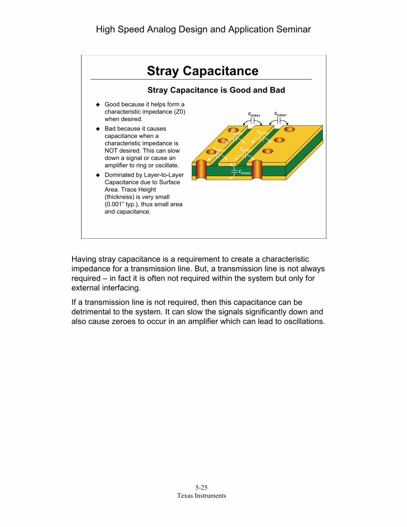
Good because it helps form acharacteristic impedance (Z0)when desired.Bad because it causescapacitance when acharacteristic impedance isNOT desired. This can slowdown a signal or cause anamplifier to ring or oscillate.Dominated by Layer-to-LayerCapacitance due to SurfaceArea. Trace Height(thickness) is very small(0.001” typ.), thus small areaand capacitance.
Having stray capacitance is a requirement to create a characteristicimpedance for a transmission line. But, a transmission line is not alwaysrequired – in fact it is often not required within the system but only forexternal interfacing.
If a transmission line is not required, then this capacitance can bedetrimental to the system. It can slow the signals significantly down andalso cause zeroes to occur in an amplifier which can lead to oscillations.

High Speed Analog Design and Application Seminar
5-26Texas Instruments
Stray Capacitance - Reducing
Possible SolutionsIf trace is NOT acharacteristicimpedance, reduce it’swidth. Not too much orelse inductance canincrease too much.Remove the GNDplane under the trace.Connect the planeselsewhere.Increase distancebetween trace andsame-Layer GNDplane.
To minimize stray capacitance, it is as easy as separating the groundplane away from the signal trace. This can involve increasing th distanceon the top layer, and/or removing the ground plane below the signal trace.
Remember, power planes are considered AC grounds and behave exactlythe same as a ground plane. So removing the power planes is asimportant as removing the ground planes in sensitive areas. This is oftenreferred to as moating.
High Speed Analog Design and Application Seminar
5-27Texas Instruments
GFSTRAY
GFZERO RRC 2
RRfπ
+=
( )GSTRAYG
F
IN
OUT RC 21RR1
VV
π+⎟⎟⎠
⎞⎜⎜⎝
⎛+=
Inverting Node (-) of Any Amplifier is VerySensitive to Stray Capacitance
As Little as 1pF of Stray Capacitance can causestability problems
Node includes Entire Trace up to the placementof RF, RG, and any other Component on (-) Node
-10
0
10
20
30
40
50
60
1 10 100 1000 10000Frequency - MHz
Am
plitu
de -
dB
Amplifier Open-Loop Gain
No Stray C
Stray C Effect
Stray C = 2.2pFGain = +1 (0dB)
RF = 1k
Zero
Intersection>>20dB/Decade
Combined Feed-back Factor
Stray Capacitance and Amplifiers
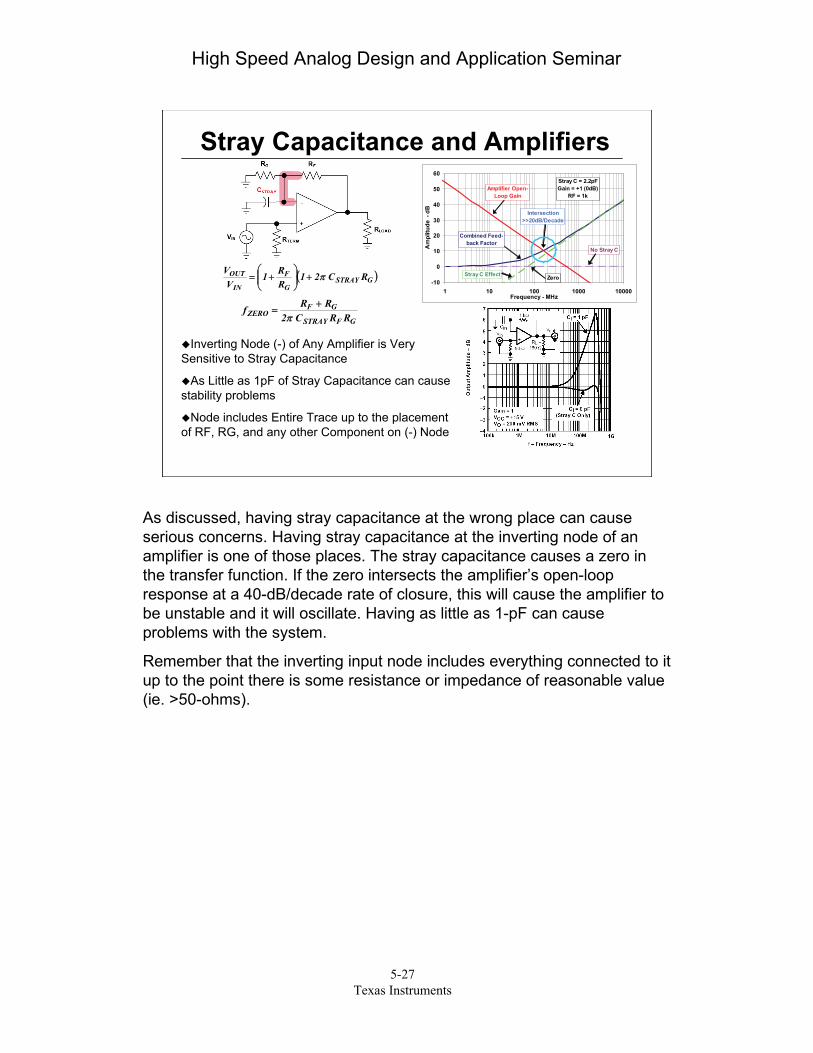
As discussed, having stray capacitance at the wrong place can causeserious concerns. Having stray capacitance at the inverting node of anamplifier is one of those places. The stray capacitance causes a zero inthe transfer function. If the zero intersects the amplifier’s open-loopresponse at a 40-dB/decade rate of closure, this will cause the amplifier tobe unstable and it will oscillate. Having as little as 1-pF can causeproblems with the system.
Remember that the inverting input node includes everything connected to itup to the point there is some resistance or impedance of reasonable value(ie. >50-ohms).

High Speed Analog Design and Application Seminar
5-28Texas Instruments
Minimizing Stray C at (-) Input
Solutions:Eliminate Ground Planesand Power Planes near (-)input node.Shorten trace by movingcomponents closer to (-)input pin.Reduce RF valueIncrease Gain of SystemUse Inverting Configurationwhich bootstraps voltage at(-) node minimizing theeffects of Stray CapacitancePlace CompensationCapacitor AcrossRF – Cancels Stray C
STRAYF
GCOMP C
RRC =
Inverting
Red
uced
RF
Valu
eCompensation
-20
-10
0
10
20
30
40
50
1 10 100 1000 10000Frequency - MHz
Am
plitu
de -
dB
Amplifier Open-Loop Gain
No Stray C
Stray C Effect
Stray C = 2.2pFGain = +1 (0dB)
RF = 50
Zero
Intersection~20dB/Decade
Combined Feed-back Factor
There are several ways to minimize the effects of stray capacitance at theinverting input node of an amplifier. These are illustrated above.
The fundamental task at hand to make the amplifier stable once again is toreduce the intersection point of the noise gain and the open-loop responseto as close to a 20-dB/decade rate of closure as possible. Even if this isclose, this should be sufficient to create a stable system.
For more information on some of these techniques, refer to the TIApplication Report entitled “Effect of Parasitic Capacitance in Op AmpCircuits”, SLOA013.

High Speed Analog Design and Application Seminar
5-29Texas Instruments
⎟⎟⎠
⎞⎜⎜⎝
⎛++
++⎟⎟
⎠
⎞⎜⎜⎝
⎛+= OSTRAY
LOAD
O
GF
O
G
F
INRC 2
RR
RRR1
RR1
VV π
OSTRAYPOLE RC 2
1fπ
≈ If RO << RF, RLOAD
Stray Capacitance and Amplifiers
No Problems if the output of Amplifier is a true Voltage sourcewith zero output impedance.But, Amplifiers DO have an Output Impedance (RO) whichcauses a pole in the response.A pole in this position causes a zero to form in the closed-loopresponse which Can lead to instability.
-10
0
10
20
30
40
50
1 10 100 1000Frequency - MHz
V / V
i - d
B
Amplifier Open-Loop Gain
Intersection Point
RO = 15ΩGain = +1 (0dB)
RF = RLoad = 1k
CLOAD = 100pF
Zero (100pF)
Stray capacitance at the output of high speed amplifier can also cause theamplifier to become unstable. This is caused by the pole formed by theamplifier's internal resistance and the capacitive loading. This RC networkcauses a zero to occur in the feedback system of the amplifier.
Just like the stray capacitance at the inverting input node, stability isdictated by the noise gain of the amplifier intersecting the open-loop gainand should be as close as possible to the 20-dB/decade rate of closure aspossible.

High Speed Analog Design and Application Seminar
5-30Texas Instruments
IncreasingGain
+
-
VIN
RFRG
RTERM
RLOADCSTRAY
V
RO
RN
CN
Increasing Noise Gain Only
+
-
VIN
RFRG
RTERM
RLOADCSTRAY
V
RO RSERIES
Adding Series R for Isolation
+
-
VIN
RFRG
RTERM
RLOADCSTRAY
V
RO RI
CC
Feedback Compensation
-10
0
10
20
30
40
50
1 10 100 1000Frequency - MHz
V / V
i - d
B
Intersection Point
Amplifier Open-Loop Gain
RO = 15ΩGain = +10 (20dB)RF = RLoad = 1k
Zero (1000pF)
CLOAD = 1000pF
Minimizing Stray C at OutputSolutions:
Eliminate Ground Planes andPower Planes under outputnode.Shorten traces by movingcomponents closer to output pin– especially Series Matching R.Increase Gain of SystemIncrease Noise Gain of SystemUse Feedback Compensation.
Solving the stability of the amplifier with a capacitive load can berelatively simple. Most common ways are to isolate the capacitive loadby some real resistance. Another way to make the amplifier stable isto increase the gain of the amplifier, or increasing the noise gain of theamplifier, which both attempt to reduce the rate of closure to the20-dB/decade goal for stability.

High Speed Analog Design and Application Seminar
5-31Texas Instruments
+
-
VIN
RF1
RG1
RTERM
+
-
RF2RG2
VOUT
CCOMP
RISO
50-Ω
+
-
VIN
RG1
RTERM
+
-
RF2RG2
VOUT
CCOMP
LTRACE
CSTRAY CINPUT +CPACKAGE
RF1
G1
F1
IN
OUTRR1
VV
+=
When Connecting an Amplifier toany other active circuit, Isolatethe amplifier with a simpleResistor (10-Ω to 250-Ω).
Otherwise the amplifier CanOscillate due to parasitics.
+
-
VIN
RF1
RG1
RTERM
+
-
RF2RG2
VOUT
CCOMP
Connecting Amplifiers
Sometimes high-speed amplifiers need a series input resistor, because packageparasitics become more and more apparent at higher signal frequencies.Package parasitics are mainly due to the leadframe pins, bondwire and the ICdie itself. The pins and bondwire can be modeled as high frequency inductors,with small capacitors between each. The die adds parasitic capacitance from thebondpad on the die to the die substrate.
All together, these parasitics can form resonant circuits, with high Q values andresonant frequencies in the hundreds of MHz. Most problems that are created bythese parasitics occur at the high impedance input of the IC. Even if the overallbandwidth of the IC is much less than the resonant frequency, the transistors inthe input stage can still be affected.
An indication of problems associated with the parasitics is higher than expectedgain peaking of the amplifier. A series input resistor will help prevent excessivegain peaking problems or even oscillation by dampening the parasitic LC circuit.Typical values for this resistor are between 10Ω to 250Ω. The value can varywidely because of different PC-board parasitics that will add to this problem.
One rule, however, exists: the smaller the package the less its parasitics and thesmaller the associated effects. Therefore, designers should choose SOIC (orsmaller) packages over DIP packages whenever possible.

High Speed Analog Design and Application Seminar
5-32Texas Instruments
After building a PC boards one often isnot sure the traces have the correctinductance or capacitance. It’s evenmore difficult to measure those valueswithout network analyzer or TDR.
See application note SB0A094 Measuring Board Parasitic in High Speed Design
A very easy way to measure trace’scapacitance is to use a ramp generator andoscilloscope, with the hook-up shown here.
4FV
2TV2
dtdV
dtdVCi 1PP
1PP ⋅⋅=⋅
== →
( ) ( ) 4FVC 50ΩdtdVC 50ΩV 1PP2PP ⋅⋅⋅==
( ) F50Ω4
1VVC
1PP
2PPM ⋅=
Measuring PCB Parasitic Capacitance
In some cases, it is desirable to know how much parasitic (stray)capacitance is actually on a trace. This may help determine stabilityproblems or to verify a characteristic impedance.
A relatively simple way to measure this is with the above test set-up. Thisset-up uses an HP8116A function generator (Vgen) to drive a tiangle wavethrough coaxial cable where one end is solder to the boards trace, groundplane, etc and two identical points are measured using an oscilloscopeterminated in 50Ω.
This method can measure capacitance to an accuracy of 30f to 50f andincludes fringing effects associated with high frequency fields.
See the TI Application Report entitled “Measuring Board Parasitics in High-Speed Analog Design”, SBOA094

High Speed Analog Design and Application Seminar
5-33Texas Instruments
A very easy way to measuretrace’s Inductance is to use aramp generator and oscilloscope,with the hook-up shown here.
TESTS
IR
VPP =
R
VF4L
2TRV2L
V PPPPPP
SmSmL
⋅⋅⋅=
⋅
⋅⋅=
PP
PP
S
Lm VF4
RVL
⋅⋅
⋅=
PP
PP
S
RM V
V RR =
Measuring PCB Parasitic Inductance
Very similar to measuring the capacitance of a PCB trace, this set-upshows how to accurately measure a PCB trace’s inductance.

High Speed Analog Design and Application Seminar
5-34Texas Instruments
50Ω
50Ω
50Ω
Example of High Speed PCB - Schematic
Multiple Caps for Low Freq.and High Freq. BypassingLook for ALL Current Pathsand their LoopsPay attention to SensitiveInverting Input NodeMatch ImpedancesFerrite Chips Used toIsolate Power SupplyCurrentsSMA ConnectorsSmall (0603) Componentsto minimize Inductance
Let’s see an example of a high speed PCB looks like. This is a schematicfor the THS4303, a very high speed voltage feedback op-amp that has abandwidth greater than 1.5-GHz. With such high bandwidth, the designmust pay attention to all high speed constraints or else the amplifier will beunstable.

High Speed Analog Design and Application Seminar
5-35Texas Instruments
Example of High Speed PCB - LayoutTOP LAYER Attributes
Signal In/Out traces are microstrip line withZ0 = 50Ω.Terminating Resistors next to Amplifier.Output Series Resistor next to Amp.100pF (NPO HF) Bypass Caps next to Amp.Larger Bypass Caps Farther Away with FerriteChips for HF isolation of currents.MULTIPLE Vias Everywhere to Allows forReduced Current Flow Area – Although not ableto be seen here, Vias are also on Componentsolder pads (See other Layers).Short, Fat Traces to reduce inductance – evenon Feedback Trace (THS4304 BW-3dB>1GHz).Large Solid Ground Plane – No SpokesSide Mount SMA connectors for Smooth SignalFlowRounded Signal Traces, no 90° bends
The top layer of the PCB is shown. Because this si a relatively simplesystem, all of the components are mounted on the top layer. Thiseliminates the signal trace via concerns to ensure the best situationpossible.
High Speed Analog Design and Application Seminar
5-36Texas Instruments
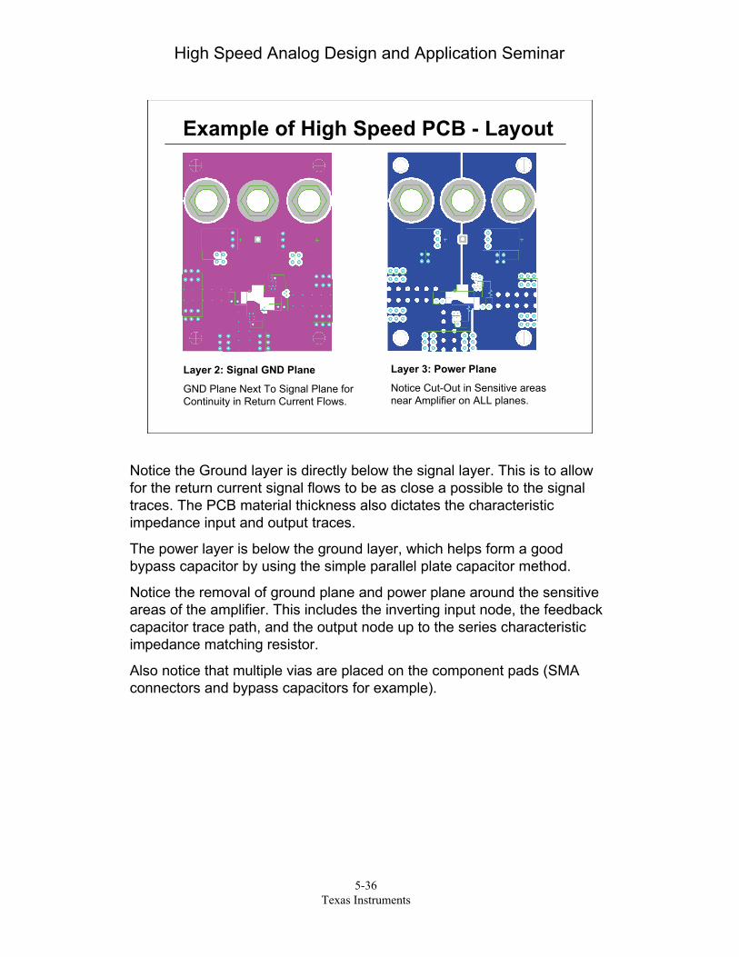
Layer 2: Signal GND Plane
GND Plane Next To Signal Plane forContinuity in Return Current Flows.
Layer 3: Power Plane
Notice Cut-Out in Sensitive areasnear Amplifier on ALL planes.
Example of High Speed PCB - Layout
Notice the Ground layer is directly below the signal layer. This is to allowfor the return current signal flows to be as close a possible to the signaltraces. The PCB material thickness also dictates the characteristicimpedance input and output traces.
The power layer is below the ground layer, which helps form a goodbypass capacitor by using the simple parallel plate capacitor method.
Notice the removal of ground plane and power plane around the sensitiveareas of the amplifier. This includes the inverting input node, the feedbackcapacitor trace path, and the output node up to the series characteristicimpedance matching resistor.
Also notice that multiple vias are placed on the component pads (SMAconnectors and bypass capacitors for example).
High Speed Analog Design and Application Seminar
5-37Texas Instruments
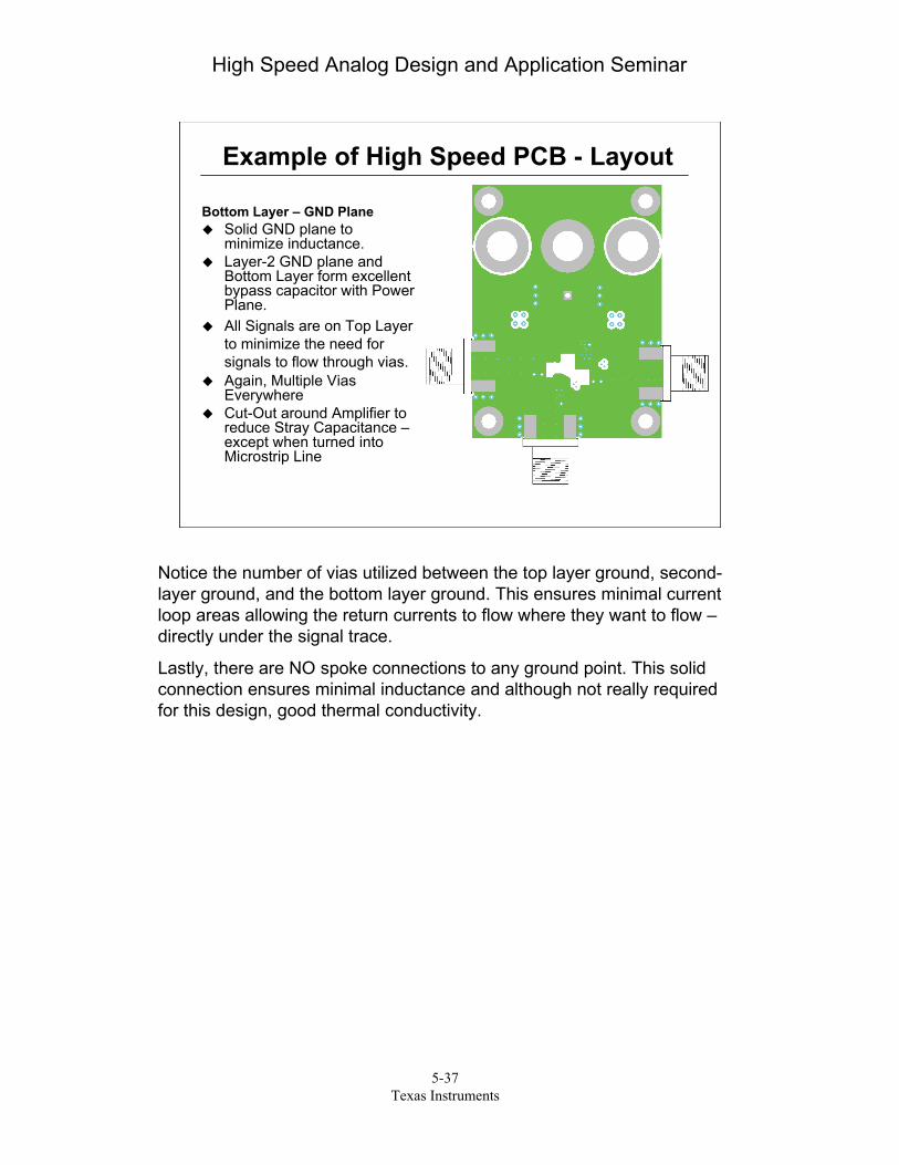
Example of High Speed PCB - Layout
Bottom Layer – GND PlaneSolid GND plane tominimize inductance.Layer-2 GND plane andBottom Layer form excellentbypass capacitor with PowerPlane.All Signals are on Top Layerto minimize the need forsignals to flow through vias.Again, Multiple ViasEverywhereCut-Out around Amplifier toreduce Stray Capacitance –except when turned intoMicrostrip Line
Notice the number of vias utilized between the top layer ground, second-layer ground, and the bottom layer ground. This ensures minimal currentloop areas allowing the return currents to flow where they want to flow –directly under the signal trace.
Lastly, there are NO spoke connections to any ground point. This solidconnection ensures minimal inductance and although not really requiredfor this design, good thermal conductivity.
High Speed Analog Design and Application Seminar
5-38Texas Instruments
-90
-80
-70
-60
-50
-40
-40 -20 0 20 40 60 80 100 120 140 160
Junction Temperature - Deg. C
THD
Thermal Issues – Silicon
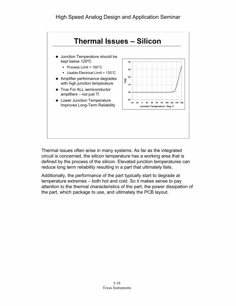
Junction Temperature should bekept below 125ºC
Process Limit = 150°CUsable Electrical Limit = 125°C
Amplifier performance degradeswith high junction temperatureTrue For ALL semiconductoramplifiers – not just TILower Junction TemperatureImproves Long-Term Reliability
Thermal issues often arise in many systems. As far as the integratedcircuit is concerned, the silicon temperature has a working area that isdefined by the process of the silicon. Elevated junction temperatures canreduce long term reliability resulting in a part that ultimately fails.
Additionally, the performance of the part typically start to degrade attemperature extremes – both hot and cold. So it makes sense to payattention to the thermal characteristics of the part, the power dissipation ofthe part, which package to use, and ultimately the PCB layout.

High Speed Analog Design and Application Seminar
5-39Texas Instruments
Top Trace
VDD
GND
Bottom Trace
Heat TransferPowerPADTM
PowerPAD Package on 4-Layer PCB
Utilizing the copper planes on the PCB for thermal conduction is anexcellent way to remove the heat from an IC. The use of a PowerPAD canallow over 3X better heat dissipation that a traditional package without thethermal pad while still using the same footprint.

High Speed Analog Design and Application Seminar
5-40Texas Instruments
Thermal ManagementMust do thermal management atthe device, the board, and thebox levels
Device: proper package heat sinking• Thermal vias to Cu planes• Unobstructed airflow• Soldering the device thermal pad to
the PCBBoard level
• Heat flow out of the board• Air flow, PCB card guides, PCB with
metal heat sinksOther Devices
• Other Active parts generate Heat• Can cause localized hot-spots on
PCB – effectively reducing thermalflow and increasing Silicon Temp.
See Application note SPRA953 – IC Package Thermal Metrics for moreinformation. The only thing that must be done is to lay out the PCBcorrectly for this pad and soldering the part to the pad. Failure to solder thepad to the PCB will result in an increase in thermal resistance and causethe junction temperature to rise which may hinder it’s performance orreduce the long term reliability.
See Application note SLMA002 –”PowerPAD Thermally EnhancedPackage” for more information.
High Speed Analog Design and Application Seminar
5-41Texas Instruments
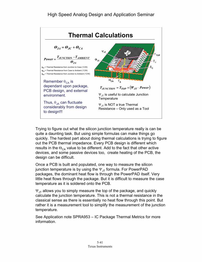
CAJCJA ΘΘΘ +=
( )PowerΨTT JTTOPJUNCTION ⋅+=
JA
AMBIENTJUNCTIONΘ
T-TPower =
Remember θCA isdependant upon package,PCB design, and externalenvironment.
Thus, θJA can fluctuateconsiderably from designto design!!!
qJC = Thermal Resistance from Junction to Case (°C/W)
qCA = Thermal Resistance from Case to Ambient (°C/W)
qJA = Thermal Resistance from Junction to Ambient (°C/W)
ΨJT is useful to calculate JunctionTemperature
ΨJT is NOT a true ThermalResistance – Only used as a Tool
Thermal Calculations
Trying to figure out what the silicon junction temperature really is can bequite a daunting task. But using simple formulas can make things goquickly. The hardest part about doing thermal calculations is trying to figureout the PCB thermal impedance. Every PCB design is different whichresults in the ΘCA value to be different. Add to the fact that other activedevices, and some passive devices too, create heating of the PCB, thedesign can be difficult.
Once a PCB is built and populated, one way to measure the siliconjunction temperature is by using the ΨJT formula. For PowerPADpackages, the dominant heat flow is through the PowerPAD itself. Verylittle heat flows through the package. But it is difficult to measure the casetemperature as it is soldered onto the PCB.
ΨJT allows you to simply measure the top of the package, and quicklycalculate the junction temperature. This is not a thermal resistance in theclassical sense as there is essentially no heat flow through this point. Butrather it is a measurement tool to simplify the measurement of the junctiontemperature.
See Application note SPRA953 – IC Package Thermal Metrics for moreinformation.