polariton nanophotonics using phase-change materials
TRANSCRIPT
ARTICLE
Polariton nanophotonics using phase-changematerialsKundan Chaudhary1,10, Michele Tamagnone 1,10*, Xinghui Yin1,10*, Christina M. Spägele 1,10,
Stefano L. Oscurato1,2, Jiahan Li3, Christoph Persch4, Ruoping Li1, Noah A. Rubin 1, Luis A. Jauregui5,
Kenji Watanabe 6, Takashi Taniguchi6, Philip Kim7, Matthias Wuttig 4, James H. Edgar3,
Antonio Ambrosio 8,9 & Federico Capasso1*
Polaritons formed by the coupling of light and material excitations enable light-matter
interactions at the nanoscale beyond what is currently possible with conventional optics.
However, novel techniques are required to control the propagation of polaritons at the
nanoscale and to implement the first practical devices. Here we report the experimental
realization of polariton refractive and meta-optics in the mid-infrared by exploiting the
properties of low-loss phonon polaritons in isotopically pure hexagonal boron nitride inter-
acting with the surrounding dielectric environment comprising the low-loss phase change
material Ge3Sb2Te6. We demonstrate rewritable waveguides, refractive optical elements
such as lenses, prisms, and metalenses, which allow for polariton wavefront engineering and
sub-wavelength focusing. This method will enable the realization of programmable minia-
turized integrated optoelectronic devices and on-demand biosensors based on high quality
phonon resonators.
https://doi.org/10.1038/s41467-019-12439-4 OPEN
1 Harvard John A. Paulson School of Engineering and Applied Sciences, Harvard University, Cambridge, MA 02138, USA. 2Department of Physics “E. Pancini”,University of Naples “Federico II”, Complesso Universitario di Monte S. Angelo, Via Cinthia 21, 80126 Naples, Italy. 3 Department of Chemical Engineering,Kansas State University, Manhattan, KS 66506, USA. 4 1. Physikalisches Institut IA, RWTH Aachen University, 52056 Aachen, Germany. 5 Department ofPhysics and Astronomy, University of California, Irvine, CA 92697, USA. 6 National Institute for Materials Science, 1-1 Namiki, Tsukuba 305-0044, Japan.7 Department of Physics, Harvard University, Cambridge, MA 02138, USA. 8 Center for Nanoscale Systems, Harvard University, Cambridge, MA 02138, USA.9 CNST – Fondazione Istituto Italiano di Tecnologia, Via Pascoli 70/3, 20133 Milano, Italy. 10These authors contributed equally: Kundan Chaudhary, MicheleTamagnone, Xinghui Yin, Christina M. Spägele. *email: [email protected]; [email protected]; [email protected]
NATURE COMMUNICATIONS | (2019) 10:4487 | https://doi.org/10.1038/s41467-019-12439-4 |www.nature.com/naturecommunications 1
1234
5678
90():,;
Polaritons in van der Waals materials behave as confinedguided optical modes, which extend as evanescent wavesinto the semi-spaces above and below1–19. Therefore, their
propagation is affected by the refractive indices of the superstrateand substrate3,4,6,8. One notable example of these polaritons arephonon polaritons (PhPs) in hexagonal boron nitride (hBN).These are not interface modes as for plasmons in noble metals:they exist instead inside the volume of hBN. The permittivityvalues are of opposite signs along different principal axes andthus polaritons exhibit hyperbolic dispersion3,8,12. The degree towhich the optical energy density of polaritons extends into thesubstrate and superstrate depends on the wavelength and thick-ness of hBN. Therefore, the excitation wavelength can be con-trolled to the point where the polariton is affected even by thevery first few nanometers of the substrate and superstrate18. Thissuggests the feasibility of substrate-engineered polariton opticswhere, instead of nanopatterning the polaritonic material itself,optical functions such as waveguiding and focusing are conferredthrough engineering the refractive index of the substrate.
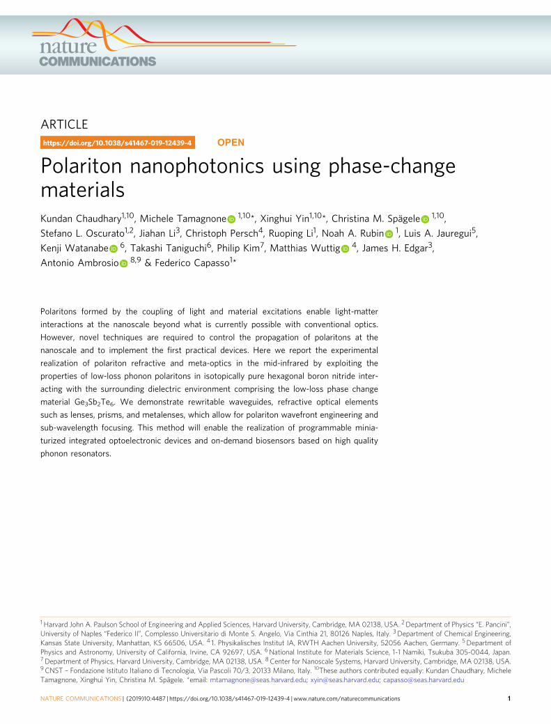
A heterostructure comprising the phase-change materialGe3Sb2Te6 (GST) and isotopically pure h11BN (referred to hBNhereinafter) is the ideal system for a proof-of-concept demon-stration of substrate-engineered polariton optics: hBN possesseslow-loss polaritons with long propagation lengths5 and GST cansupport two vastly different refractive indices in its amorphous andcrystalline phases (na= 4.2 and nc= 6.1), which can co-exist atroom temperature20–29. While GST has been previously employedto demonstrate switchable PhP resonators in quartz27, more
complex applications including metasurfaces remained elusive dueto limited propagation lengths of PhPs in quartz. On the otherhand, VO2 has been used as a substrate with hBN to achievetemperature-dependent polariton dispersion28. However, thisapproach suffers from limitations because VO2’s different phasescannot co-exist at the same temperature, and thus in close spatialproximity as is desirable for the realisation of optical devices. Here,we show an hBN-GST heterostructure in which arbitrary patternscan be written, erased, and re-written to control the PhP propa-gation. We achieve this by defining several structures, rangingfrom waveguides30,31 to diffraction-limited focusing metalenses.Specifically, we use low-loss PhPs in isotopically pure hBN (11Bisotopes with >99% purity5) with longer propagation lengths,which we combine with Ge3Sb2Te6, a stoichiometry with parti-cularly low absorption in the mid-infrared (mid-IR)29. We work inthe second Reststrahlen band (from 1361–1610 cm−1), which isassociated with in-plane optical phonons5,6.
ResultsReconfigurable 2D refractive polariton lenses. Figure 1a showsthe hBN-GST heterostructure used in this work. As PhPs arestrongly confined, a thin layer of 55 nm of GST below hBN(195 nm of thickness) is sufficient to significantly alter polaritonpropagation. To create the heterostructure, we sputter a thin filmof GST on a CaF2 substrate (in an amorphous phase as-depos-ited), protect it with a 15 nm layer of ZnS:SiO2 against oxidationand then transfer exfoliated hBN to form the top layer. A pulsed
405 nm laser
ZnS:SiO2
GST
CaF2
a b
d e f
hBN
n = 4.2 n = 6.1 n = 4.2
Amorphous Crystalline Amorphous
Effe
ctiv
e in
dex
10
20
50
5
2 50 nm hBN
200 nm hBN100 nm hBN
c-GSTa-GST
1400 1450 1500 1550
Frequency (cm–1)
1
Objective c
hBN
Air
ZnS:SiO2GST
CaF2
z
c-GST
a-GST
Ex
Optical
SampleIR light
Time (ns)
Tcryst
Tmelt
Erase
Write
Melted
Crystalline
Amorphous
s-SNOM tip
hBN edge
s-SNOM
Fig. 1 Reconfigurable polaritons in hBN-GST heterostructures. aWriting setup and device cross-section. A 405 nm focused laser beam is used to write andreconfigure devices on GST underneath hBN (transparent at 405 nm). b Longer, low-power laser pulses are used to crystallise GST and shorter high-powerpulses are used to melt it to restore the amorphous phase. c Electric field profile of polaritons for the a-GST and c-GST cases. The electric field confinementis larger in c-GST (due to its larger refractive index) than in a-GST. Ex represents the electric field along the direction of polariton propagation. Thicknessesfor each layer are 195 nm for hBN, 15 nm for ZnS:SiO2, 55 nm for GST and 1 mm for CaF2, which is then considered semi-infinite. Refractive indices are 1.7for ZnS:SiO2, 4.2 and 6.1 for GST in amorphous and crystalline phases, respectively, 1.37 for CaF2, while hBN is modelled with the Lorentz model presentedin Supplementary Note 1. d Calculated dispersion relation of the effective index neff for different hBN thicknesses on a-GST and c-GST. e Polaritons arelaunched by the hBN edge when light impinges on the sample. The launched polaritons interact with the written devices and their propagation is imagedusing scattering-type scanning near field optical microscopy (s-SNOM). f Example of optical and s-SNOM images. Scale bar is 5 µm
ARTICLE NATURE COMMUNICATIONS | https://doi.org/10.1038/s41467-019-12439-4
2 NATURE COMMUNICATIONS | (2019) 10:4487 | https://doi.org/10.1038/s41467-019-12439-4 | www.nature.com/naturecommunications
laser diode is used to write and erase patterns by selectivelycrystallising or re-amorphising GST22 (Fig. 1b).
The PhP mode profile is affected by the state (either crystallineor amorphous) of the GST beneath it (Fig. 1c), which can bequantified by using the effective index neff ¼ c=vph, where c isthe speed of light and vph is the PhP’s phase velocity. Figure 1dshows the dispersion of neff for different hBN thicknesses on botha-GST (neff,a) and c-GST (neff,c), respectively. We use scattering-type scanning near field optical microscopy (s-SNOM) tocharacterise the polaritons launched at hBN edges, whichpropagate across the optical elements (Fig. 1e, f)8,13,18.
Polariton propagation in heterostructures with a- or c-GST isanalogous to light propagation in two different materials (such asair and glass). The continuity of the electric field at the boundarybetween two regions implies Snell’s law32:
neff ;cneff ;a
¼ sin θað Þsin θcð Þ ; ð1Þ
where θ is the propagation angle in corresponding regions withrespect to the interface normal.
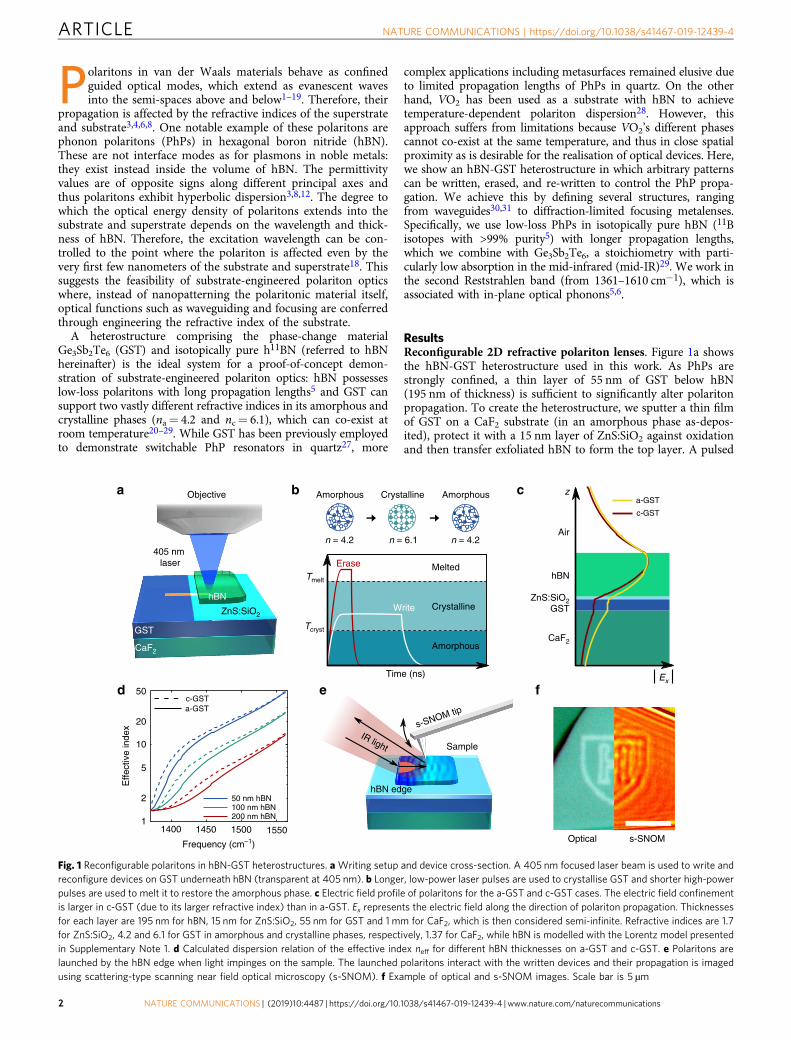
Many conventional optical devices (such as lenses and prisms)are governed by Snell’s law, suggesting that similar componentscan be implemented in our hBN-GST heterostructure. The firstexample to illustrate this principle is a refractive lens, specifically,a plano-convex semi-circular lens to focus PhPs (Fig. 2a).
We write and erase a semi-circular plano-convex lens (radius(R= 5 μm)) twice and subsequently replace it with a plano-concavelens of the same radius (Fig. 2b–f). The straight hBN edge launcheslinear waves (the planar equivalent of three-dimensional planewaves), which are either focused by the plano-convex lens ordiverged by the plano-concave lens (Fig. 1g, h). The lateral size of thefocal spot is 2 μm (29% of the free space wavelength), which isdiffraction limited according to the Abbe limit computed for the 2Dwaves (i.e. 2.08 μm). The numerical aperture (NA) with respect topolaritons in a-GST is 0.55, while the NA with respect to vacuum is2.11, which is higher than unity due to the high confinement of PhPs.
We performed phase-resolved s-SNOM measurements aftereach writing and erasing step. Using amplitude and phaseinformation, the wavefronts of the polaritons can be clearlyimaged (see Supplementary Note 4 for more details onmeasurements and image processing). The resulting imagesconfirm focusing, which is shown by the narrow waist in thetransmitted beam (Fig. 1i). Characteristic curved wavefronts canbe seen before and after the focal spot. The position of the focalspot of the lens is measured from the images and compared withtheoretical computation with two different methods (Fig. 2j). Thefirst method is based on computing the focal spot using rayoptics, while the second, more accurate, method models thefocused beam as a Gaussian beam, and identifies the focal spot asthe beam waist32 (see more details in the Supplementary Note 2,Supplementary Fig. 1 and Supplementary Table 1).
Concave
s
Convex
c
a
s
Ray opticsGaussian beam opticsMeasurement
Foc
ussi
ng d
ista
nce s
(µm
)
a
hBN
edg
e
b c d e f
1st erasing, 1455 cm–1 3rd writing, 1490 cm–1
Frequency (cm–1)
14204
6
8
10
12
14
16
1440 1460 1480
g i j
k l m
h1st erasing 2nd writing 2nd erasing 3rd writing
hBN
edg
e
1st writing
2nd writing, 1455 cm–1
neff,a neff,c
R
neff,a
2D
1st writing, 1455 cm–1
Fig. 2 Rewritable flat polaritonic lenses. a Plano-convex lens schematics for 3D and 2D semi-spherical and semi-circular lenses. In the 2D case the materialrefractive index is replaced by the effective index of the polaritons on amorphous or crystalline GST. b–f Optical images of the written lens. The writtenpatterns are clearly visible in the pictures because the refractive index of a-GST and c-GST also differs at visible wavelengths. First a plano-convex semi-circular lens (radius R= 5 µm) is written and measured, then it is erased, re-written (with same dimensions), erased again and finally the same area isreconfigured into a plano-concave lens (R= 5 µm). g, h Diagram of wavefronts for 2D plano-convex and plano-concave lenses, respectively. i s-SNOMimage of the plano-convex lens after the first writing. A focal spot is clearly visible. j Dependence of the focal length on the wavenumber. Error barsrepresent the uncertainty of the fitted waist position, approximately one fringe). k s-SNOM scan after first erasing. l s-SNOM scan of the re-written plano-convex lens. m s-SNOM scan of the plano-concave lens (third writing). s-SNOM images in i, l and m have been processed to remove the fringes outsidethe main beam (see Supplementary Note 4, Supplementary Table 3 and Supplementary Fig. 5). Scale bars are 5 µm
NATURE COMMUNICATIONS | https://doi.org/10.1038/s41467-019-12439-4 ARTICLE
NATURE COMMUNICATIONS | (2019) 10:4487 | https://doi.org/10.1038/s41467-019-12439-4 |www.nature.com/naturecommunications 3
After erasing, only polaritons with linear wavefronts that arelaunched by the hBN edge are visible, whereas focusing is fullyrestored when the lens is re-written (Fig. 2k, l). Furthermore,reconfiguring the same area to a plano-concave lens results incurved wavefronts associated with diverging PhPs (Fig. 2m).
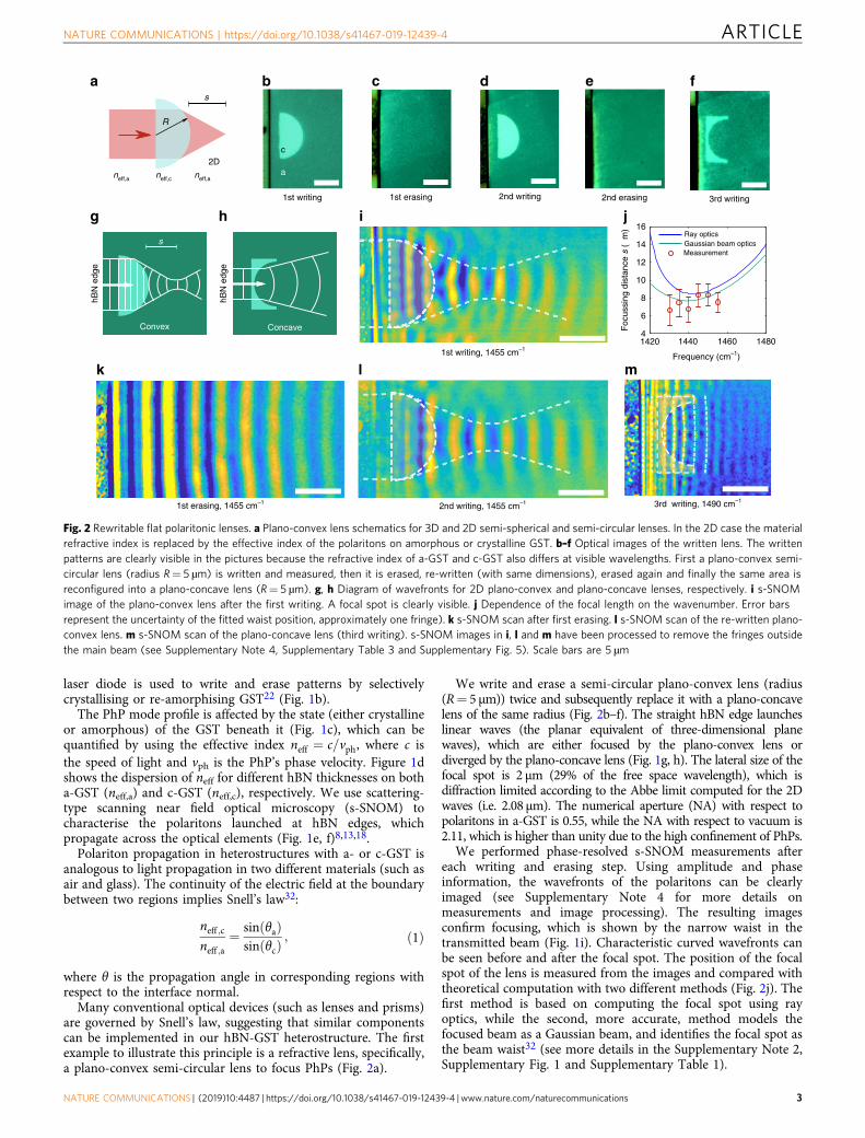
Prisms and waveguides. The successful implementation of lensescan be extended to other common devices such as prisms andwaveguides (Fig. 3). Planar prisms are simply triangles and followSnell’s law (Fig. 3a). We wrote a prism and two waveguides (withdifferent widths) close to the hBN edge so that edge-launched wavescan interact with them (Fig. 3b–e). The prism is designed to be anisosceles right triangle with one side parallel to the hBN edge suchthat edge-launched waves enter orthogonal to it. When traversingthe hypotenuse, the polariton propagation direction (k vector) isbent downwards (as expected from Snell’s law), as is clearly visiblein the s-SNOM measurements in the form of bent fringes (Fig. 3f).
The waveguides consist of c-GST lines with widths (0.7 and1.1 µm) smaller or comparable to the guided polariton wave-length. They provide additional in-plane confinement such thatthe propagating mode is truly one-dimensional and is confinedalong the waveguide. Here, the c-GST line acts as the waveguidecore, while a-GST serves as cladding. The s-SNOM measurementin Fig. 3g shows that the wavefront spacing decreases inside thewaveguides, as expected from confined modes. Furthermore, thecompression is greater for the wider waveguide. This implies thatthe waveguide effective index neff,wg is larger when the width ofthe waveguide increases, which agrees with the behaviour knownfrom conventional dielectric waveguides where the core sizeaffects the effective index of the mode. In both the conventionaland the polariton cases, the value of the waveguide effective indexlies between the indices of the core and cladding material, that is,neff ;a � neff ;wg � neff ;c: We verified this behaviour by numericallycalculating the waveguide dispersion relation (see Methods) andcomparing the results to s-SNOM measurements taken atdifferent frequencies (Fig. 3h). Figure 3i shows a cross-section
of a guided mode obtained from numerical simulation, illustrat-ing how polaritons are confined both vertically and laterally.
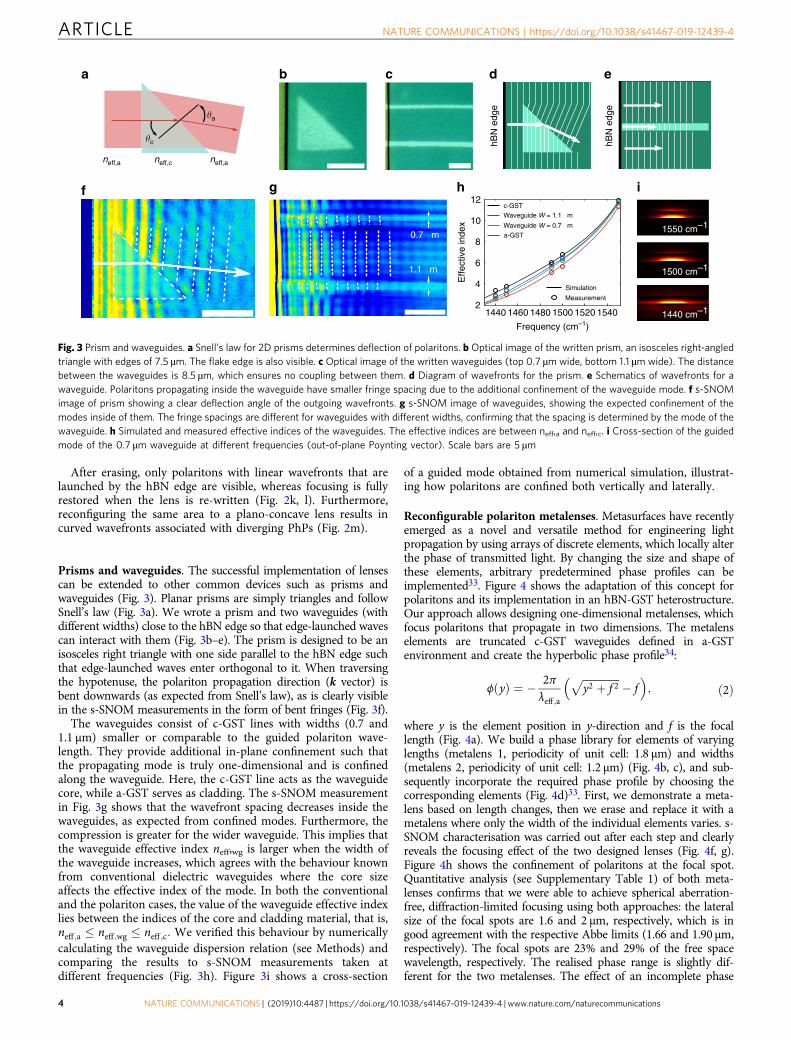
Reconfigurable polariton metalenses. Metasurfaces have recentlyemerged as a novel and versatile method for engineering lightpropagation by using arrays of discrete elements, which locally alterthe phase of transmitted light. By changing the size and shape ofthese elements, arbitrary predetermined phase profiles can beimplemented33. Figure 4 shows the adaptation of this concept forpolaritons and its implementation in an hBN-GST heterostructure.Our approach allows designing one-dimensional metalenses, whichfocus polaritons that propagate in two dimensions. The metalenselements are truncated c-GST waveguides defined in a-GSTenvironment and create the hyperbolic phase profile34:
ϕ yð Þ ¼ � 2πλeff ;a
ffiffiffiffiffiffiffiffiffiffiffiffiffiffi
y2 þ f 2p
� f� �
; ð2Þ
where y is the element position in y-direction and f is the focallength (Fig. 4a). We build a phase library for elements of varyinglengths (metalens 1, periodicity of unit cell: 1.8 µm) and widths(metalens 2, periodicity of unit cell: 1.2 µm) (Fig. 4b, c), and sub-sequently incorporate the required phase profile by choosing thecorresponding elements (Fig. 4d)33. First, we demonstrate a meta-lens based on length changes, then we erase and replace it with ametalens where only the width of the individual elements varies. s-SNOM characterisation was carried out after each step and clearlyreveals the focusing effect of the two designed lenses (Fig. 4f, g).Figure 4h shows the confinement of polaritons at the focal spot.Quantitative analysis (see Supplementary Table 1) of both meta-lenses confirms that we were able to achieve spherical aberration-free, diffraction-limited focusing using both approaches: the lateralsize of the focal spots are 1.6 and 2 µm, respectively, which is ingood agreement with the respective Abbe limits (1.66 and 1.90 µm,respectively). The focal spots are 23% and 29% of the free spacewavelength, respectively. The realised phase range is slightly dif-ferent for the two metalenses. The effect of an incomplete phase
a b c d e
f g h
�c
�a
neff,a neff,c neff,a
0.7 µm
1.1 µm
i
1550 cm–1
1500 cm–1
1440 cm–1
hBN
edg
e
hBN
edg
e
Measurement
Simulation
c-GST
a-GST
Waveguide W = 1.1 µm
Waveguide W = 0.7 µm
1440 1460 1480 1500 1520 1540
Frequency (cm–1)
2
4
6
8
10
12
Effe
ctiv
e in
dex
Fig. 3 Prism and waveguides. a Snell’s law for 2D prisms determines deflection of polaritons. b Optical image of the written prism, an isosceles right-angledtriangle with edges of 7.5 µm. The flake edge is also visible. c Optical image of the written waveguides (top 0.7 µm wide, bottom 1.1 µm wide). The distancebetween the waveguides is 8.5 µm, which ensures no coupling between them. d Diagram of wavefronts for the prism. e Schematics of wavefronts for awaveguide. Polaritons propagating inside the waveguide have smaller fringe spacing due to the additional confinement of the waveguide mode. f s-SNOMimage of prism showing a clear deflection angle of the outgoing wavefronts. g s-SNOM image of waveguides, showing the expected confinement of themodes inside of them. The fringe spacings are different for waveguides with different widths, confirming that the spacing is determined by the mode of thewaveguide. h Simulated and measured effective indices of the waveguides. The effective indices are between neff,a and neff,c. i Cross-section of the guidedmode of the 0.7 µm waveguide at different frequencies (out-of-plane Poynting vector). Scale bars are 5 µm
ARTICLE NATURE COMMUNICATIONS | https://doi.org/10.1038/s41467-019-12439-4
4 NATURE COMMUNICATIONS | (2019) 10:4487 | https://doi.org/10.1038/s41467-019-12439-4 | www.nature.com/naturecommunications
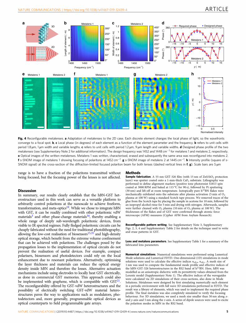
range is to have a fraction of the polaritons transmitted withoutbeing focused, but the focusing power of the lenses is not affected.
DiscussionIn summary, our results clearly establish that the hBN-GST het-erostructure used in this work can serve as a versatile platform toarbitrarily control polaritons at the nanoscale to achieve freeform,transformation, and meta-optics19. While we chose to integrate hBNwith GST, it can be readily combined with other polaritonic vdWmaterials3 and other phase-change materials34, thereby enabling awhole range of deeply sub-wavelength polaritonic devices, fromvisible to IR spectral regimes. Fully fledged polaritonic circuits can becheaply fabricated without the need for traditional photolithography,allowing the low-cost realisation of biosensors15,35 and high-densityoptical storage, which benefit from the extreme volume confinementthat can be achieved with polaritons. The challenges posed by thepropagation losses to the implementation of optical circuits do notprevent the realisation of useful devices. For example, compactpolarisers, biosensors and photodetectors could rely on the localenhancement due to resonant polaritons. Alternatively, optimisingthe layer thickness and materials can reduce the optical energydensity inside hBN and therefore the losses. Alternative actuationmechanisms include using electrodes to locally heat GST electrically,as done in commercial GST memories. This approach could alsobe implemented with graphene, which is compatible with GST21.The reconfigurability offered by GST-vdW heterostructures and thepossibility of electrically switching GST-vdW material hetero-structures paves the way to applications such as modulators, pho-todetectors and, more generally, programmable optical devices asoptical counterparts to field programmable gate arrays.
MethodsSample fabrication. A 55-nm GST-326 film (with 15 nm of ZnS:SiO2 protectionlayer) was sputter coated onto a 1-mm-thick CaF2 substrate. Lithography wasperformed to define alignment markers (positive tone photoresist S1813 spincoated at 3000 RPM and baked at 115 °C for 90 s), followed by Pt sputtering(30 nm) and lift-off at room temperature. Isotopically pure h11BN flakes weremechanically exfoliated onto the substrate after plasma activation (5 min of O2
plasma at 100W) using a standard Scotch tape process. We removed traces of theglue from the Scotch tape by placing the sample in acetone for 10 min, followed byan isopropyl alcohol rinse for 5 min and drying with nitrogen. Afterwards, sampleswere further cleaned with O2 plasma (10 min of O2 plasma at 100W). Thethicknesses of the flakes and of GST were confirmed through atomic forcemicroscope (AFM) measures (Cypher AFM from Asylum Research).
Reconfigurable pattern writing. See Supplementary Note 3, SupplementaryFigs. 2, 3, 4 and Supplementary Table 2 for details on the technique used to writeand erase patterns in GST.
Lens and metalens parameters. See Supplementary Table 1 for a summary of thefabricated lens parameters.
Numerical simulations. Numerical simulations were performed using LumericalMode solutions and Lumerical FDTD. One-dimensional (1D) simulations in modesolutions were used to calculate the effective indices neff,a, neff,c. A mesh size of1 nm was used to compute the fundamental mode profile and effective indices ofthe hBN-GST-326 heterostructures in the RS2 band of h11BN. Here, hBN wasmodelled as an anisotropic dielectric with its permittivity values obtained from theLorentz model (Supplementary Note 1). The effective indices of the waveguideswere calculated via 2D simulations of their cross-sections, also done in ModeSolutions. Metalenses were designed by first simulating numerically each elementin a periodic environment with full wave 3D simulations performed in FDTD. Theresult was a library of elements, which was used to implement the required phaseprofile. The final metalens was also completely simulated to verify the focusingbehaviour. For 3D simulations, we used a mesh size smaller than 50 nm along x-and y-axis and 5 nm along the z-axis. A series of dipole sources were used to excitethe polariton modes in hBN in the RS2 band.
3Da
e f g h
b c d
2D
8
6
4
2
01400 1450 1500 1450 1500 –15
15
10
5
0
–5
–10
–150 0.5Normalised intensity
1
–5 0 5
y (µm)
y (µ
m)
10 15–10
–15 –5 0 5 10 15–10
01400
0.2
0.4
0.6
0.8
1
1.2300°
250°
200°
150°
100°
50°
0°
300°
400°
250°
350°
360
0
360
0
200°
150°
100°
50°
0°
Wid
th o
f ele
men
t (µm
)
Metalens 2
Metalens 2
Metalens 2
Required phase
Pha
se (
°)P
hase
(°)
Designed phase
Metalens 2
Metalens 1
Metalens 1 Metalens 2Metalens 1
Frequency (cm–1) Frequency (cm–1)
Metalens 1
Metalens 1
Leng
th o
f ele
men
t (µm
)
Fig. 4 Reconfigurable metalenses. a Adaptation of metalenses to the 2D case. Each discrete element changes the local phase of light, so the wavefrontsconverge to a focal spot. b, c Local phase (in degrees) of each element as a function of the element parameter and the frequency. b refers to unit cells withperiod 1.8 µm, 1 µm width and variable lengths. c refers to unit cells with period 1.2 µm, 9 µm length and variable widths. d Designed phase profile of the twometalenses (see Supplementary Note 2 for additional information). The design frequency was 1452 and 1448 cm−1 for metalens 1 and metalens 2, respectively.e Optical images of the written metalenses. Metalens 1 was written, characterised, erased and subsequently the same area was reconfigured into metalens 2.f s-SNOM image of metalens 1 showing focusing of polaritons at 1452 cm−1. g s-SNOM image of metalens 2 at 1445 cm−1. h Intensity profile (square of s-SNOM signal) at the cross-section of the diffraction-limited focused polariton beam for both lenses (dashed vertical lines in f, g). Scale bars are 5 µm
NATURE COMMUNICATIONS | https://doi.org/10.1038/s41467-019-12439-4 ARTICLE
NATURE COMMUNICATIONS | (2019) 10:4487 | https://doi.org/10.1038/s41467-019-12439-4 |www.nature.com/naturecommunications 5

s-SNOM measurements. The near-field scans were obtained using a commercialsystem from NeaSpec. Tapping-mode AFM is used (tapping amplitude of 130 nm,Pt-Ir-coated tips with resonant frequency of ~300 kHz, tip diameter of ~20 nm). Aquantum cascade laser array from Daylight Solutions was used as a tuneable mid-IR source for imaging. The phase-amplitude images are obtained using a pseudo-heterodyne demodulation. The images of lenses and metalenses were processedusing the technique shown in the Supplementary Note 4 to isolate the polaritonsfocused by the structure. In all cases, polaritons are self-launched by the edges36.See Supplementary Note 5 and Supplementary Figs. 6, 7, 8 for additionalmeasurements.
Data availabilityAll data are available from the authors upon request. Please contact M.T. for any requestof materials and data.
Received: 14 August 2019; Accepted: 5 September 2019;
References1. Ma, W. et al. In-plane anisotropic and ultra-low-loss polaritons in a natural
van der Waals crystal. Nature 562, 557–563 (2018).2. Alonso-González, P. et al. Acoustic terahertz graphene plasmons revealed by
photocurrent nanoscopy. Nat. Nanotechnol. 12, 31–35 (2017).3. Basov, D., Fogler, M. & de Abajo, F. G. Polaritons in van der Waals materials.
Science 354, aag1992 (2016).4. Low, T. et al. Polaritons in layered two-dimensional materials. Nat. Mater. 16,
182–194 (2017).5. Giles, A. J. et al. Ultralow-loss polaritons in isotopically pure boron nitride.
Nat. Mater. 17, 134–139 (2018).6. Dai, S. et al. Tunable phonon polaritons in atomically thin van der Waals
crystals of boron nitride. Science 343, 1125–1129 (2014).7. Li, P. et al. Infrared hyperbolic metasurface based on nanostructured van der
Waals materials. Science 359, 892–896 (2018).8. Ambrosio, A. et al. Selective excitation and imaging of ultraslow phonon
polaritons in thin hexagonal boron nitride crystals. Light Sci. Appl. 7, 27(2018).
9. Caldwell, J. D. et al. Low-loss, infrared and terahertz nanophotonics usingsurface phonon polaritons. Nanophotonics 4, 44–68 (2015).
10. Yoxall, E. et al. Direct observation of ultraslow hyperbolic polaritonpropagation with negative phase velocity. Nat. Photon. 9, 674–678 (2015).
11. Kumar, A., Low, T., Fung, K. H., Avouris, P. & Fang, N. X. Tunablelight–matter interaction and the role of hyperbolicity in graphene-hbn system.Nano Lett. 15, 3172–3180 (2015).
12. Tamagnone, M. et al. Ultra-confined mid-infrared resonant phononpolaritons in van der Waals nanostructures. Sci. Adv. 4, eaat7189 (2018).
13. Grigorenko, A. N. et al. Graphene plasmonics. Nat. Photon. 6, 749–758 (2012).14. Hillenbrand, R., Taubner, T. & Keilmann, F. Phonon-enhanced light–matter
interaction at the nanometre scale. Nature 418, 159–162 (2002).15. Rodrigo, D. et al. Mid-infrared plasmonic biosensing with graphene. Science
349, 165–168 (2015).16. Chen, J. et al. Optical nano-imaging of gate-tunable graphene plasmons.
Nature 487, 77–81 (2012).17. Alonso-González, P. et al. Controlling graphene plasmons with resonant metal
antennas and spatial conductivity patterns. Science 344, 1369–1373 (2014).18. Chaudhary, K. et al. Engineering phonon polaritons in van der Waals
heterostructures to enhance in-plane optical anisotropy. Sci. Adv. 5, eaau7171(2019).
19. Ashkan, V. & Engheta, N. Transformation optics using graphene. Science 332,1291–1294 (2011).
20. Wuttig, M., Bhaskaran, H. & Taubner, T. Phase-change materials for non-volatile photonic applications. Nat. Photon. 11, 465–476 (2017).
21. Lin, H. et al. Chalcogenide glass-on-graphene photonics. Nat. Photon. 11,798–805 (2017).
22. Wuttig, M. & Yamada, N. Phase-change materials for rewriteable data storage.Nat. Mater. 6, 824–832 (2007).
23. Tuma, T. et al. Stochastic phase-change neurons. Nat. Nanotechnol. 11,693–699 (2016).
24. Ríos, C. et al. Integrated all-photonic non-volatile multi-level memory. Nat.Photon. 9, 725–732 (2015).
25. Hosseini, P., Wright, C. D. & Bhaskaran, H. An optoelectronic frameworkenabled by low-dimensional phase-change films. Nature 511, 206–211 (2014).
26. Yin, X. et al. Beam switching and bifocal zoom lensing using active plasmonicmetasurfaces. Light Sci. Appl. 6, e17016 (2017).
27. Li, P. et al. Reversible optical switching of highly confined phonon–polaritonswith an ultrathin phase-change material. Nat. Mater. 15, 870–875 (2016).
28. Folland, T. G. et al. Reconfigurable infrared hyperbolic metasurfaces usingphase change materials. Nat. Commun. 9, 4371 (2018).
29. Michel, A.-K. U. et al. Using low-loss phase-change materials for mid-infraredantenna resonance tuning. Nano Lett. 13, 3470–3475 (2013).
30. Steinberger, B. et al. Dielectric stripes on gold as surface plasmon waveguides.Appl. Phys. Lett. 88, 094104 (2006).
31. Rude, M. et al. Active control of surface plasmon waveguides with a phasechange material. ACS Photonics 2, 669–674 (2015).
32. Yariv, A. & Yeh, P. Photonics (Oxford University Press, New York, 2007).33. Khorasaninejad, M. et al. Metalenses at visible wavelengths: diffraction-limited
focusing and subwavelength resolution imaging. Science 352, 1190–1194 (2016).34. Raty, J. ‐Y. et al. A quantum‐mechanical map for bonding and properties in
solids. Adv. Mater. 2018, 1806280 (2018).35. Autore, M. et al. Boron nitride nanoresonators for phonon-enhanced
molecular vibrational spectroscopy at the strong coupling limit. Light Sci.Appl. 7, 17172 (2017).
36. Gilburd, L. et al. Hexagonal boron nitride self-launches hyperbolic phononpolaritons. J. Phys. Chem. Lett. 8, 2158–2162 (2017).
AcknowledgementsThis work was supported by the NSF EFRI, award no. 1542807. This work was performedin part at the Centre for Nanoscale Systems (CNS), a member of the National Nano-technology Coordinated Infrastructure Network (NNCI), which is supported by theNational Science Foundation under NSF award no. 1541959. M.T. acknowledges the sup-port of the Swiss National Science Foundation (SNSF) grant no. 168545 and 177836. S.L.O.acknowledges “Fondazione Angelo Della Riccia”, and the programme for “InternationalMobility of Researchers” of the University of Naples “Federico II” (Italy), for financialsupport. The h11BN crystal growth was supported by the National Science Foundation,award number 1538127. K.W. and T.T. acknowledge support from the Elemental StrategyInitiative conducted by the MEXT, Japan and the CREST (JPMJCR15F3), JST.
Author contributionsK.C., M.T. and X.Y. conceived the project. M.T., K.C., X.Y., C.M.S., A.A. and F.C. devisedexperiments. X.Y. and C.S. designed and implemented the setup for writing patterns onGST-326 with help from R.L. and N.A.R. J.L. and J.H.E. provided isotopically pure h11BNfor final devices. C.P. and M.W. optimised and deposited the GST layer on the substrate.K.W., T.T., L.A.J. and P.K. provided natural abundance hBN for initial tests. X.Y. andC.M.S. wrote and erased patterns on h11BN/GST-326 heterostructures. K.C., M.T., S.L.O.,C.M.S. and A.A. performed s-SNOM and AFM scans. K.C., M.T., X.Y. and C.M.S. per-formed FDTD simulations. M.T. and K.C. analysed the experimental data. F.C. led theproject. All authors contributed to discussions and manuscript preparation.
Competing interestsThe authors declare no competing interests.
Additional informationSupplementary information is available for this paper at https://doi.org/10.1038/s41467-019-12439-4.
Correspondence and requests for materials should be addressed to M.T., X.Y. or F.C.
Peer review information Nature Communications thanks the anonymous reviewers fortheir contribution to the peer review of this work.
Reprints and permission information is available at http://www.nature.com/reprints
Publisher’s note Springer Nature remains neutral with regard to jurisdictional claims inpublished maps and institutional affiliations.
Open Access This article is licensed under a Creative CommonsAttribution 4.0 International License, which permits use, sharing,
adaptation, distribution and reproduction in any medium or format, as long as you giveappropriate credit to the original author(s) and the source, provide a link to the CreativeCommons license, and indicate if changes were made. The images or other third partymaterial in this article are included in the article’s Creative Commons license, unlessindicated otherwise in a credit line to the material. If material is not included in thearticle’s Creative Commons license and your intended use is not permitted by statutoryregulation or exceeds the permitted use, you will need to obtain permission directly fromthe copyright holder. To view a copy of this license, visit http://creativecommons.org/licenses/by/4.0/.
© The Author(s) 2019
ARTICLE NATURE COMMUNICATIONS | https://doi.org/10.1038/s41467-019-12439-4
6 NATURE COMMUNICATIONS | (2019) 10:4487 | https://doi.org/10.1038/s41467-019-12439-4 | www.nature.com/naturecommunications