active oxide nanophotonics - thesis.library.caltech.edu
TRANSCRIPT
ACTIVE OXIDE NANOPHOTONICS
Thesis by
Matthew J. Dicken
In Partial Fulfillment of the Requirements
for the Degree of
Doctor of Philosophy
CALIFORNIA INSTITUTE OF TECHNOLOGY
Pasadena, California
2009
(Defended March 25, 2009)

ii
© 2009
Matthew J. Dicken
All Rights Reserved

iii
ACKNOWLEDGEMENTS
I would like to gratefully acknowledge funding from the Center for Science and Engineering
of Materials and the Army Research Lab. I would like to thank Harry Atwater for the
seemingly endless resources and my committee for their attention. It has been my pleasure to
work with the handful of fabulous people at Caltech. Finally, thank you Megan for your
support and patience.
iv
ABSTRACT
Materials that can be manipulated electrically or mechanically to induce a change in
their intrinsic properties are highly relevant when suitably integrated with current
technologies. These “active” materials, such as oxide-based ferroelectrics or materials with
easily accessible changes of phase, find extensive use as mechanical resonators, solid-state
memories, and optical modulators. Barium titanate, a tetragonal ferroelectric at room
temperature, is a prime example of a material both mechanically and optically active. This
thesis deals primarily with the deposition of active, oxide-based materials and their
integration into device structures where either the mechanical or optical properties are
exploited.
The technologically interesting paradigms within which these active oxide materials
have been investigated are microelectromechanical systems, plasmonics, and metamaterials.
Microelectromechanical systems are devices that have been micromachined and rely on an
applied voltage to induce a mechanical response. Mechanically active materials, such as
piezoelectrics or ferroelectrics, can increase the response of these devices. Plasmonics deals
with electromagnetic waves resonantly coupled into free electron oscillations at a metal-
dielectric interface or metal nanoparticle. Coupling to these resonant modes allows surface
plasmon polaritons to propagate along the metal with a nonlinear dispersion. Metamaterials
are ordered, subwavelength, metal inclusions in a dielectric, which respond collectively to
electromagnetic radiation. This response can yield a material permittivity or permeability not
found in nature. The optical properties of metamaterials lead to effects such as negative
index response and super lensing, and can be used to design optical cloaking structures.
Here, devices utilizing these effects are investigated with an eye toward tuning or switching
their resonant response using optically active oxide thin films.
This manuscript follows the evolution of active oxide thin films from deposition,
through design of plasmonic devices and active metamaterials, finite difference modeling of
these structures, and finally experimental validation. First, deposition and material
integration techniques for oxide-based thin films will be discussed. The role of molecular
beam epitaxy, pulsed laser deposition, and ion beam assisted deposition as material growth
techniques are investigated. Development of a multitude of oxide materials using these
techniques including barium titanate, strontium ruthenate, vanadium oxide, and magnesium
oxide will be covered. The following two sections deal with the mechanical and optical
v
properties of barium titanate thin films as they are studied and utilized to design and fabricate
active devices. Films were characterized mechanically, using nanoindentation and
piezoresponse force microscopy, and optically with variable angle spectroscopic
ellipsometry. The subsequent section deals with the design, fabrication, and experimental
validation of an active optical device based on surface plasmon polariton wavevector
modulation via electrooptic modulation of a barium titanate thin film. Interferometers based
on pairs of parallel slits fabricated in silver films on barium titanate are used to investigate
optical modulation due to both domain switching and the electrooptic effect. Finally, active
metamaterials are discussed through the investigation of a new material, vanadium oxide, as
it is deposited and characterized, and the results used to design and fabricate active, split-ring
resonator metamaterial structures.
vi
TABLE OF CONTENTS
Acknowledgements. . . . . . . . . . . . . . . . . . . . . . . . . . . . . . . . . . . . . . . . . . . . . . . . . . . . . . . . .iii
Abstract . . . . . . . . . . . . . . . . . . . . . . . . . . . . . . . . . . . . . . . . . . . . . . . . . . . . . . . . . . . . . . . . . .iv
Table of Contents . . . . . . . . . . . . . . . . . . . . . . . . . . . . . . . . . . . . . . . . . . . . . . . . . . . . . . . . . .vi
List of Figures. . . . . . . . . . . . . . . . . . . . . . . . . . . . . . . . . . . . . . . . . . . . . . . . . . . . . . . . . . . . . .x
Chapter 1: Introduction . . . . . . . . . . . . . . . . . . . . . . . . . . . . . . . . . . . . . . . . . . . . . . . . . . . . .1
1.1 Piezoelectricity and Ferroelectricity. . . . . . . . . . . . . . . . . . . . . . . . . . . . . . . . . . .1
1.1.1 Orientation Effects. . . . . . . . . . . . . . . . . . . . . . . . . . . . . . . . . . . . . . . . .3
1.2 Active Materials . . . . . . . . . . . . . . . . . . . . . . . . . . . . . . . . . . . . . . . . . . . . . . . . . .5
1.2.1 Mechanically Active Materials . . . . . . . . . . . . . . . . . . . . . . . . . . . . . . .5
1.2.2 Fatigue . . . . . . . . . . . . . . . . . . . . . . . . . . . . . . . . . . . . . . . . . . . . . . . . . .6
1.2.3 Optically Active Oxides. . . . . . . . . . . . . . . . . . . . . . . . . . . . . . . . . . . . .8
1.3 Nanophotonics . . . . . . . . . . . . . . . . . . . . . . . . . . . . . . . . . . . . . . . . . . . . . . . . . . .9
1.3.1 Plasmonics. . . . . . . . . . . . . . . . . . . . . . . . . . . . . . . . . . . . . . . . . . . . . . .9
1.3.2 Metamaterials. . . . . . . . . . . . . . . . . . . . . . . . . . . . . . . . . . . . . . . . . . . .13
1.4 Thesis Scope. . . . . . . . . . . . . . . . . . . . . . . . . . . . . . . . . . . . . . . . . . . . . . . . . . . .15
1.4.1 Part I: Thin Film Deposition and Characterization Techniques. . . . .15
1.4.2 Part II: Mechanical and Optical Characterization of Active Oxides .16
1.4.3 Part III: Active Metal-Oxide Nanophotonics. . . . . . . . . . . . . . . . . . . 16
Part I: Thin Film Deposition and Characterization Techniques . . . . . . . . . . . . . . . . . . 18
Chapter 2: Background. . . . . . . . . . . . . . . . . . . . . . . . . . . . . . . . . . . . . . . . . . . . . . . . . . . . .19
2.1 Deposition Techniques. . . . . . . . . . . . . . . . . . . . . . . . . . . . . . . . . . . . . . . . . . . .19
2.1.1 Ion Beam Assisted Deposition of MgO. . . . . . . . . . . . . . . . . . . . . . . .19
vii
2.1.2 Molecular Beam Epitaxy-MBE. . . . . . . . . . . . . . . . . . . . . . . . . . . . . .20
2.1.3 Pulsed Laser Deposition-PLD . . . . . . . . . . . . . . . . . . . . . . . . . . . . . . .21
2.2 Characterization Techniques . . . . . . . . . . . . . . . . . . . . . . . . . . . . . . . . . . . . . . . 23
2.2.1 Reflection High-Energy Electron Diffraction-RHEED. . . . . . . . . . . .23
2.2.2 Piezoresponse Force Microscopy-PFM. . . . . . . . . . . . . . . . . . . . . . . .25
2.2.3 Variable Angle Spectroscopic Ellipsometry-VASE . . . . . . . . . . . . . .27
2.3 Conclusions . . . . . . . . . . . . . . . . . . . . . . . . . . . . . . . . . . . . . . . . . . . . . . . . . . . . 30
Chapter 3: Oxide Thin Film Growth Techniques. . . . . . . . . . . . . . . . . . . . . . . . . . . . . . . .31
3.1 Ion Beam Assisted Deposition-MgO . . . . . . . . . . . . . . . . . . . . . . . . . . . . . . . . .31
3.2 Molecular Beam Epitaxy-BaTiO3. . . . . . . . . . . . . . . . . . . . . . . . . . . . . . . . . . . .35
3.3 Pulsed Laser Deposition-BaTiO3, SrTiO3, SrRuO3, and VO2. . . . . . . . . . . . . . 40
3.4 Conclusions . . . . . . . . . . . . . . . . . . . . . . . . . . . . . . . . . . . . . . . . . . . . . . . . . . . . 44
Part II: Mechanical and Optical Characterization of Active Oxides . . . . . . . . . . . . . . . 45
Chapter 4: Active Oxide Thin Films–Mechanical Studies. . . . . . . . . . . . . . . . . . . . . . . . .46
4.1 Orientation Effects on Barium Titanate Polarization. . . . . . . . . . . . . . . . . . . . . 46
4.1.1 Barium Titanate Thin Films on Conductive Substrates. . . . . . . . . . . .46
4.1.2 Conclusion . . . . . . . . . . . . . . . . . . . . . . . . . . . . . . . . . . . . . . . . . . . . .52
4.2 Mechanical Domain Switching . . . . . . . . . . . . . . . . . . . . . . . . . . . . . . . . . . . . . 52
4.2.1 Nanoindentation. . . . . . . . . . . . . . . . . . . . . . . . . . . . . . . . . . . . . . . . . 52
4.3 Conclusions. . . . . . . . . . . . . . . . . . . . . . . . . . . . . . . . . . . . . . . . . . . . . . . . . . . . 56
Chapter 5: Active Oxide Thin Films–Optical Studies. . . . . . . . . . . . . . . . . . . . . . . . . . . . 57
5.1 Background. . . . . . . . . . . . . . . . . . . . .. . . . . . . . . . . . . . . . . . . . . . . . . . . . . . . . 57
5.2 Optical Properties of Textured Barium Titanate Thin Films. . . . . . . . . . . . . . . 58
5.2.1 Barium Titanate Thin Film Growth. . . . . . . . . . . . . . . . . . . . . . . . . . .59
viii
5.2.2 Characterization. . . . . . . . . . . . . . . . . . . . . . . . . . . . . . . . . . . . . . . . . .60
5.2.3 Conclusions . . . . . . . . . . . . . . . . . . . . . . . . . . . . . . . . . . . . . . . . . . . . .70
5.3 Optical Properties of Vanadium Oxide Thin Films. . . . . . . . . . . . . . . . . . . . . . 70
Part III: Active Metal-Oxide Nanophotonics . . . . . . . . . . . . . . . . . . . . . . . . . . . . . . . . . . 72
Chapter 6: Active Metal-Oxide Plasmonics. . . . . . . . . . . . . . . . . . . . . . . . . . . . . . . . . . . . 73
6.1 Introduction. . . . . . . . . . . . . . . . . . . . . . . . . . . . . . . . . . . . . . . . . . . . . . . . . . . . .73
6.2 Device Design. . . . . . . . . . . . . . . . . . . . . . . . . . . . . . . . . . . . . . . . . . . . . . . . . . .75
6.2.1 Plasmonic Interferometer Device Stack. . . . . . . . . . . . . . . . . . . . . . . .75
6.2.2 Analytical Model. . . . . . . . . . . . . . . . . . . . . . . . . . . . . . . . . . . . . . . . .76
6.2.3 Finite Difference Time Domain Simulations. . . . . . . . . . . . . . . . . . . .78
6.3 Experiment. . . . . . . . . . . . . . . . . . . . . . . . . . . . . . . . . . . . . . . . . . . . . . . . . . . . . 82
6.4 Conclusions . . . . . . . . . . . . . . . . . . . . . . . . . . . . . . . . . . . . . . . . . . . . . . . . . . . . 87
Chapter 7: Active Metamaterials in the Near-Infrared. . . . . . . . . . . . . . . . . . . . . . . . . . .88
7.1 Introduction . . . . . . . . . . . . . . . . . . . . . . . . . . . . . . . . . . . . . . . . . . . . . . . . . . . . 88
7.2 Device Design . . . . . . . . . . . . . . . . . . . . . . . . . . . . . . . . . . . . . . . . . . . . . . . . . . 89
7.3 Metamaterial Response in the Near-Infrared. . . . . . . . . . . . . . . . . . . . . . . . . . . 92
7.3.1 Planar, VO2-Based, Hybrid-SRR Metamaterials . . . . . . . . . . . . . . . . 92
7.3.2 Self-Aligned, Metal/VO2-Based, Hybrid-SRR Metamaterials . . . . . .94
7.3.3 Active, Frequency-Tunable, Hybrid-SRR Based Metamaterials . . . . 96
7.4 Simulated Optical Response in Metamaterials . . . . . . . . . . . . . . . . . . . . . . . . . 98
7.5 Conclusions . . . . . . . . . . . . . . . . . . . . . . . . . . . . . . . . . . . . . . . . . . . . . . . . . . . 100
Chapter 8: Optical Properties of Combinatorial Metal Films. . . . . . . . . . . . . . . . . . . . .101
8.1 Introduction . . . . . . . . . . . . . . . . . . . . . . . . . . . . . . . . . . . . . . . . . . . . . . . . . . . 101
8.2 Combinatorial Thin Films . . . . . . . . . . . . . . . . . . . . . . . . . . . . . . . . . . . . . . . . 102

ix
8.3 Metal Alloy Optical Characterization . . . . . . . . . . . . . . . . . . . . . . . . . . . . . . . 105
8.4 Metal Alloy Simulations . . . . . . . . . . . . . . . . . . . . . . . . . . . . . . . . . . . . . . . . . 107
8.5 Conclusions . . . . . . . . . . . . . . . . . . . . . . . . . . . . . . . . . . . . . . . . . . . . . . . . . . . 109
References . . . . . . . . . . . . . . . . . . . . . . . . . . . . . . . . . . . . . . . . . . . . . . . . . . . . . . . . . . . . . . 111
x
LIST OF FIGURES
Figure 1.1. Barium titanate domain structure. . . . . . . . . . . . . . . . . . . . . . . . . . . . . . . . . . . . . .2
Figure 1.2. Orientation effects on piezoresponse in ferroelectrics. . . . . . . . . . . . . . . . . . . . . .4
Figure 1.3. Mechanical work vs cycling frequency. . . . . . . . . . . . . . . . . . . . . . . . . . . . . . . . . 6
Figure 1.4. Polarization fatigue. . . . . . . . . . . . . . . . . . . . . . . . . . . . . . . . . . . . . . . . . . . . . . . . .7
Figure 1.5. Barium titanate based electrooptic devices. . . . . . . . . . . . . . . . . . . . . . . . . . . . . . 9
Figure 1.6. Plasmon dispersion and resonance. . . . . . . . . . . . . . . . . . . . . . . . . . . . . . . . . . . .12
Figure 1.7. Nanoparticle plasmon resonance. . . . . . . . . . . . . . . . . . . . . . . . . . . . . . . . . . . . ..12
Figure 1.8. Metal-insulator-metal plasmon waveguide. . . . . . . . . . . . . . . . . . . . . . . . . . . . . 13
Figure 1.9. Split-ring resonators. . . . . . . . . . . . . . . . . . . . . . . . . . . . . . . . . . . . . . . . . . . . . . .14
Figure 2.1. Ultra-high vacuum molecular beam epitaxy system . . . . . . . . . . . . . . . . . . . . . .20
Figure 2.2. Pulsed laser deposition system. . . . . . . . . . . . . . . . . . . . . . . . . . . . . . . . . . . . . . .22
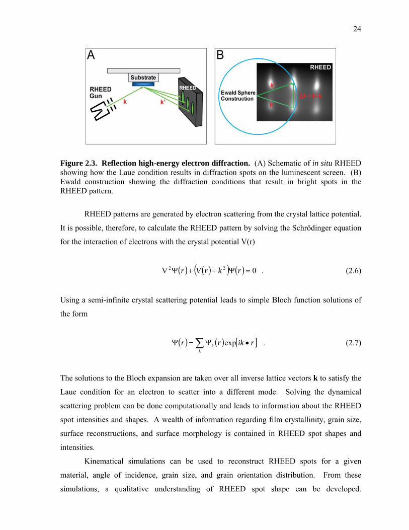
Figure 2.3. Reflection high-energy electron diffraction. . . . . . . . . . . . . . . . . . . . . . . . . . . . .24
Figure 2.4. Piezoresponse force microscopy. . . . . . . . . . . . . . . . . . . . . . . . . . . . . . . . . . . . . 26
Figure 2.5. Hysterisis loops. . . . . . . . . . . . . . . . . . . . . . . . . . . . . . . . . . . . . . . . . . . . . . . . . . 26
Figure 2.6. Ellipsometry. . . . . . . . . . . . . . . . . . . . . . . . . . . . . . . . . . . . . . . . . . . . . . . . . . . . .28
Figure 3.1. Ion beam assisted deposition-MgO RHEED development. . . . . . . . . . . . . . . . . 32
Figure 3.2. Ion beam assisted deposition-MgO x-ray diffraction comparison. . . . . . . . . . . .33
Figure 3.3. S3N4 transmission electron microscope arrays. . . . . . . . . . . . . . . . . . . . . . . . . . .34
Figure 3.4. RHEED intensity oscillations. . . . . . . . . . . . . . . . . . . . . . . . . . . . . . . . . . . . . . . .36
Figure 3.5. Barium titanate RHEED comparison. . . . . . . . . . . . . . . . . . . . . . . . . . . . . . . . . .37
xi
Figure 3.6. Barium titanate x-ray diffraction comparison. . . . . . . . . . . . . . . . . . . . . . . . . . . 38
Figure 3.7. Barium titanate atomic/piezo force microscopy. . . . . . . . . . . . . . . . . . . . . . . . . .39
Figure 3.8. Piezoresponse Hysterisis Loops. . . . . . . . . . . . . . . . . . . . . . . . . . . . . . . . . . . . . .39
Figure 3.9. Pulsed laser deposition barium titanate . . . . . . . . . . . . . . . . . . . . . . . . . . . . . . . .40
Figure 3.10. Pulsed laser deposition strontium titanate. . . . . . . . . . . . . . . . . . . . . . . . . . . . .41
Figure 3.11. Compositionally graded barium strontium titanate. . . . . . . . . . . . . . . . . . . . . . 42
Figure 3.12. Pulsed laser deposition strontium ruthenate . . . . . . . . . . . . . . . . . . . . . . . . . . . 42
Figure 3.13. Pulsed laser deposition barium titanate on strontium ruthenate . . . . . . . . . . . . 43
Figure 3.14. Vanadium (II) oxide x-ray diffraction. . . . . . . . . . . . . . . . . . . . . . . . . . . . . . . . 44
Figure 4.1. Barium titanate on conductive substrates-x-ray diffraction comparison. . . . . . . 48
Figure 4.2. Barium titanate on conductive substrates-RHEED comparison. . . . . . . . . . . . . .48
Figure 4.3. Barium titanate on conductive substrates-AFM/PFM comparison . . . . . . . . . . .50
Figure 4.4. Barium titanate on conductive substrates-hysterisis. . . . . . . . . . . . . . . . . . . . . . .51
Figure 4.5. Bulk barium titanate domain analysis. . . . . . . . . . . . . . . . . . . . . . . . . . . . . . . . . 54
Figure 4.6. Bulk barium titanate AFM/PFM analysis. . . . . . . . . . . . . . . . . . . . . . . . . . . . . . .55
Figure 4.7. Bulk barium titanate nanoindentation. . . . . . . . . . . . . . . . . . . . . . . . . . . . . . . . . 56
Figure 5.1. Barium titanate RHEED comparison: plasma growth vs molecular O2. . . . . . . . 61
Figure 5.2. Barium titanate x-ray diffraction comparison: plasma growth vs molecular O2 62
Figure 5.3. Barium titanate AFM/PFM: plasma growth . . . . . . . . . . . . . . . . . . . . . . . . . . . . 64
Figure 5.4. Barium titanate on MgO-VASE: plasma growth . . . . . . . . . . . . . . . . . . . . . . . . 65
Figure 5.5. Barium titanate on MgO-VASE: molecular O2 growth. . . . . . . . . . . . . . . . . . . .65
Figure 5.6. Barium titanate on IBAD MgO-VASE: plasma growth. . . . . . . . . . . . . . . . . . . 66
Figure 5.7. Barium titanate on IBAD MgO-VASE: molecular O2 growth. . . . . . . . . . . . . . 66
xii
Figure 5.8. Barium titanate index of refraction comparison. . . . . . . . . . . . . . . . . . . . . . . . . .68
Figure 5.9. Pulsed laser deposition barium titanate-VASE. . . . . . . . . . . . . . . . . . . . . . . . . . 69
Figure 5.10. Vanadium oxide-VASE: Heating Experiment. . . . . . . . . . . . . . . . . . . . . . . . . .71
Figure 5.11. Vanadium oxide complex index of refraction . . . . . . . . . . . . . . . . . . . . . . . . . .71
Figure 6.1. Double-slit metal-ferroelectric plasmonic modulator. . . . . . . . . . . . . . . . . . . . . 75
Figure 6.2. Double-slit SPP interferometer array. . . . . . . . . . . . . . . . . . . . . . . . . . . . . . . . . .77
Figure 6.3. FDTD device simulations. . . . . . . . . . . . . . . . . . . . . . . . . . . . . . . . . . . . . . . . . . .79
Figure 6.4. Poynting vector streamlines . . . . . . . . . . . . . . . . . . . . . . . . . . . . . . . . . . . . . . . . 80
Figure 6.5. FDTD and analytical model validation. . . . . . . . . . . . . . . . . . . . . . . . . . . . . . . . 81
Figure 6.6. Experimental double-slit transmission modulation . . . . . . . . . . . . . . . . . . . . . . .83
Figure 6.7. Experimental observation of SPP modulation. . . . . . . . . . . . . . . . . . . . . . . . . . . 84
Figure 6.8. Modulation hysterisis in double-slit arrays . . . . . . . . . . . . . . . . . . . . . . . . . . . . .85
Figure 6.9. Optical validation of domain switching. . . . . . . . . . . . . . . . . . . . . . . . . . . . . . . .86
Figure 7.1. Vanadium oxide-based hybrid-SRR metamaterials . . . . . . . . . . . . . . . . . . . . . . 90
Figure 7.2. Scanning electron micrograph images of coupled-SRR arrays. . . . . . . . . . . . . . 91
Figure 7.3. Planar, vanadium oxide-based, SRR metamaterials . . . . . . . . . . . . . . . . . . . . . . 93
Figure 7.4. Self-aligned hybrid-SRR based metamaterials. . . . . . . . . . . . . . . . . . . . . . . . . . .95
Figure 7.5. Active, frequency-tunable, hybrid-SRR based metamaterials. . . . . . . . . . . . . . .97
Figure 7.6. FDTD simulations of vanadium oxide-based hybrid-SRR metamaterials. . . . . .99
Figure 7.7. Simulations of vanadium oxide-based hybrid-SRR metamaterial concepts . . .100
Figure 8.1. Electron dispersive spectroscopy: metal alloys . . . . . . . . . . . . . . . . . . . . . . . . .103
Figure 8.2. Transmission electron microscopy: Ag-Au . . . . . . . . . . . . . . . . . . . . . . . . . . . .104

xiii
Figure 8.3. Variable angle spectroscopic ellipsometry: metal alloys . . . . . . . . . . . . . . . . . 105
Figure 8.4. Metal alloy optical constants. . . . . . . . . . . . . . . . . . . . . . . . . . . . . . . . . . . . . . . 107
Figure 8.5. Simulated metal alloy SPP dispersion relations. . . . . . . . . . . . . . . . . . . . . . . . .108
Figure 8.6. Extinction in metal alloy nanoparticles . . . . . . . . . . . . . . . . . . . . . . . . . . . . . . .109
1
Chapter 1
Introduction
Extrinsic material properties have been studied since the dawn of humankind.
Understanding the composition and properties of the materials that make up our universe is
of utmost importance for our technological progression. Throughout time, the classification
of solid materials has evolved from purely utilitarian (hard, soft), to a knowledge of the
elements (gold, lead), and finally to an understanding of materials on an atomistic scale. The
study of materials and their interactions with nature has led to the discovery of such
important properties as conductivity, magnetism, piezoelectricity, ferroelectricity, refraction,
optical waveguiding, and a host of other effects. It is not an overstatement that all
technologically relevant achievements have, at their roots, no small amount of materials
research.
Of particular interest in the age of logic devices are materials and effects that can be
controlled externally. Materials that demonstrate electrical or optical properties that can be
modified by an external force are largely investigated or engineered to act as switching
elements. Here, we investigate such active material properties as piezoelectricity,
ferroelectricity, the electrooptic effect, and insulator-metal phase transitions.
1.1 Piezoelectricity and Ferroelectricity
Many interesting properties in solid materials can be derived from their crystal
symmetry. Solid systems of atoms can be classified into 32 symmetric point groups, 20 of
which are noncentrosymmetric. It is from this select class of materials that the piezoelectric
and ferroelectric effects arise. The electromechanical properties of materials were first
studied in the later 1800s by Pierre and Jacques Curie. Their initial work characterized the
piezoelectric effect from studies of Rochelle salt and quartz. Further work on Rochelle salt
led to the discovery of ferroelectric effect by Valasek in 1920 (Nye 1957). Ferroelectric
materials exhibit spontaneous electrical polarization due to a structural displacement of
atoms in the crystal unit cell. Interactions between adjacent unit cells lead to polarization
domain formation similar to ferromagnetic domains. The quintessential ferroelectric
2
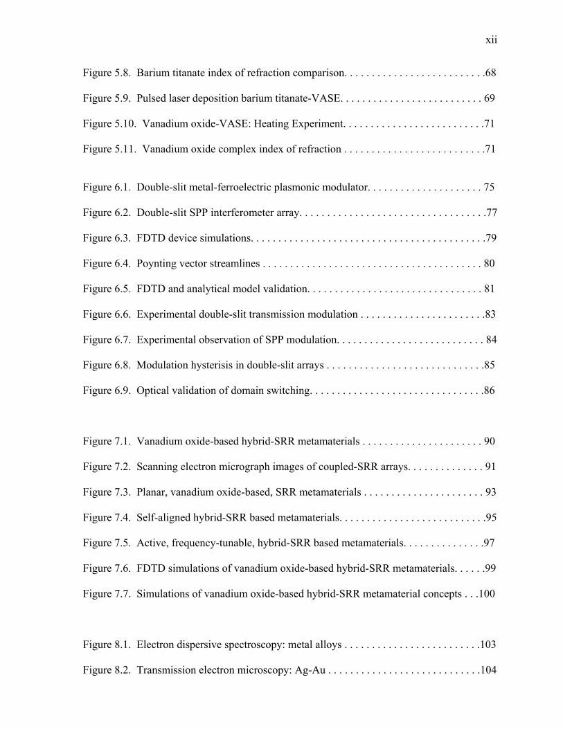
material, barium titanate, BaTiO3, (BTO) and its domain patterns are shown in figure 1.1
(Bhattacharya et al. 2003).
The ferroelectric effect in materials, including BTO, exists as a result of a polar axis
found in 10 of the 20 noncentrosymmetric crystal point groups. Ferroelectric materials are
characterized by the existence of a switchable dipole moment within the crystal unit cell. All
ferroelectric materials also exhibit the piezoelectric effect, defined as a mechanically induced
polarization of the lattice (Fatuzzo et al. 1967). The piezoelectric effect (equation (1.1))
linearly relates the induced charge density, Di, due to an applied stress, jk, in a material.
Figure 1.1. Barium titanate domain structure. Tetragonal BaTiO3 above (A) and below (B) its Curie temperature, Tc, demonstrating the displacement of the oxygen tetrahedron from the central Ti atom and subsequent spontaneous polarization. Ferroelectric domains form below the Curie temperature imaged using a polarized optical microscope at 0° (C) and 90° (D).
3
jkijki dD (1.1)
Here, dijk is a third-rank tensor of piezocoefficients that relate the charge and stress in 3-D. It
is more common to encounter the converse piezoelectric effect (equation (1.2)), defined as
the strain, ij, induced due to an applied electric field, Ek.
kkijij Ed (1.2)
The piezoelectric coefficients form a symmetric third-rank tensor, and the symmetry of the
material can be used to reduce many of the elements to zero. Those elements which are non-
zero are determined by the symmetry point group of the crystal. The perovskite oxide
ferroelectrics, BTO, strontium titanate (STO) and lead titanate (PTO), have a point group of
P4MM and the resulting tensor has the form
000
00000
00000
333131
15
15
ddd
d
d
. (1.3)
This tensor shows two shear components, d31 and d15, and one direct response, d33, for a
given directional effect (electric field, stress, etc.). The form of the response tensor will be
identical for other linear effects on the P4MM crystal structure, and therefore the same
coefficients will be non-zero in the tensor describing the electrooptic coefficients. The
dependence of orientation on these properties must be understood and controlled during
ferroelectric device design and fabrication.
1.1.1 Orientation Effects
Crystal orientation plays a large role in the response of a material to external effects.
The tensorial nature of bulk material properties is well known and equations can be written to
describe the combined response including all coefficients (equation (1.4)) and they can be
represented in 3-D as polar plots (figure 1.2) (Harnagea 2001).
4
21315
333 sincoscos dddd zz (1.4)
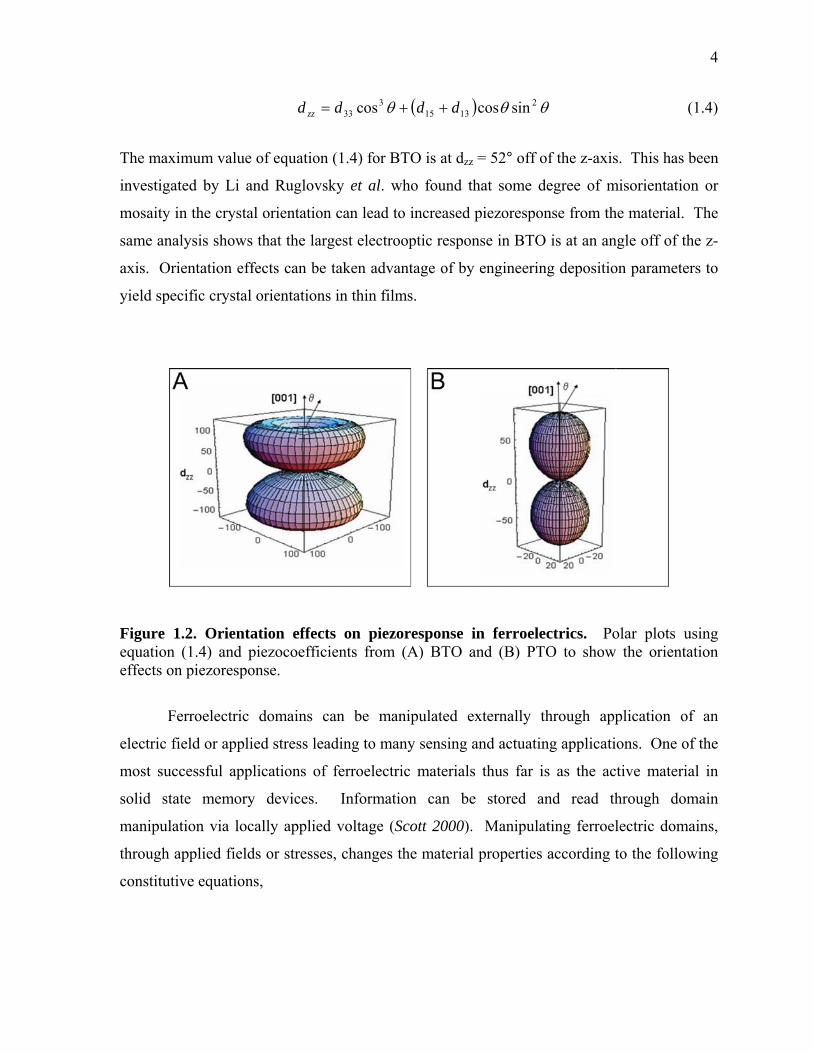
The maximum value of equation (1.4) for BTO is at dzz = 52° off of the z-axis. This has been
investigated by Li and Ruglovsky et al. who found that some degree of misorientation or
mosaity in the crystal orientation can lead to increased piezoresponse from the material. The
same analysis shows that the largest electrooptic response in BTO is at an angle off of the z-
axis. Orientation effects can be taken advantage of by engineering deposition parameters to
yield specific crystal orientations in thin films.
Figure 1.2. Orientation effects on piezoresponse in ferroelectrics. Polar plots using equation (1.4) and piezocoefficients from (A) BTO and (B) PTO to show the orientation effects on piezoresponse.
Ferroelectric domains can be manipulated externally through application of an
electric field or applied stress leading to many sensing and actuating applications. One of the
most successful applications of ferroelectric materials thus far is as the active material in
solid state memory devices. Information can be stored and read through domain
manipulation via locally applied voltage (Scott 2000). Manipulating ferroelectric domains,
through applied fields or stresses, changes the material properties according to the following
constitutive equations,
5
kkijjii EeC ,, , (1.5)
nnlmmll EeD ,, , (1.6)
which show the coupled nature of elastic stress (), displacement (D), elastic strain () and
applied field (E) with their proportionality constants (C, , ) (Damjanovic 1998, Nye 1957).
Understanding and engineering the mechanical and optical activity of ferroelectric materials
opens new avenues for device design.
1.2 Active Materials
A central theme of this thesis work is coaxing tunable mechanical, optical, or
electrical responses from thin film materials through an external force. Barium titanate, the
material of focus for the first half of this thesis, exhibits ferroelectric and electrooptic
properties, which can induce both mechanical and optical changes. Vanadium (II) oxide
(VO2) has a low insulator-metal transition temperature which causes the material to become
conductive and highly absorbing in the infrared portion of the spectrum. Mechanical and
optical activity in BTO will be discussed in the following sections. Effects of the VO2 phase
transition and its application to active metamaterial designs will be examined in chapter 7.
1.2.1 Mechanically Active Materials
Ferroelectric thin films exhibit mechanical responses to applied stress or electric
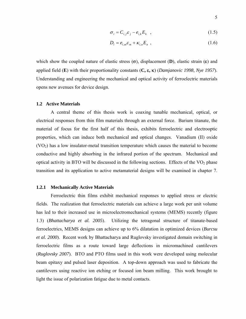
fields. The realization that ferroelectric materials can achieve a large work per unit volume
has led to their increased use in microelectromechanical systems (MEMS) recently (figure
1.3) (Bhattacharya et al. 2005). Utilizing the tetragonal structure of titanate-based
ferroelectrics, MEMS designs can achieve up to 6% dilatation in optimized devices (Burcsu
et al. 2000). Recent work by Bhattacharya and Ruglovsky investigated domain switching in
ferroelectric films as a route toward large deflections in micromachined cantilevers
(Ruglovsky 2007). BTO and PTO films used in this work were developed using molecular
beam epitaxy and pulsed laser deposition. A top-down approach was used to fabricate the
cantilevers using reactive ion etching or focused ion beam milling. This work brought to
light the issue of polarization fatigue due to metal contacts.
6
Figure 1.3. Mechanical work vs cycling frequency. Plot of mechanically active materials used in microelectromechanical systems showing their relative work output at a given cycling frequency (Krulevitch et al. 1996).
1.2.2 Fatigue
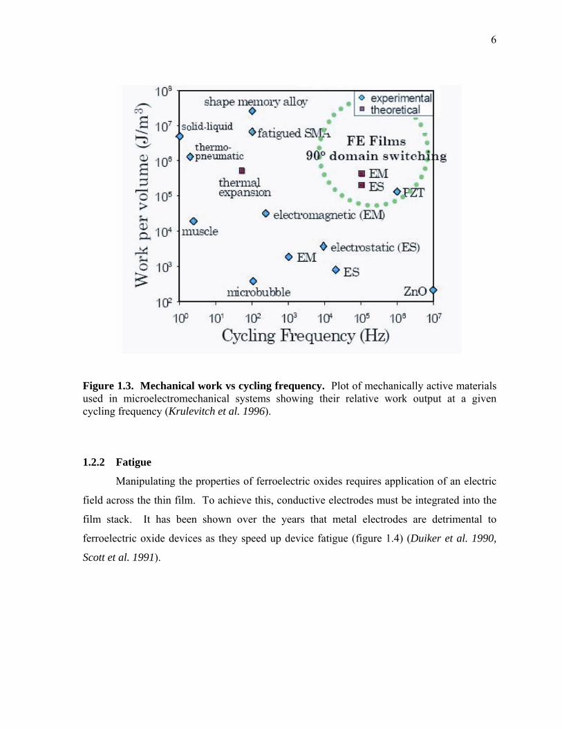
Manipulating the properties of ferroelectric oxides requires application of an electric
field across the thin film. To achieve this, conductive electrodes must be integrated into the
film stack. It has been shown over the years that metal electrodes are detrimental to
ferroelectric oxide devices as they speed up device fatigue (figure 1.4) (Duiker et al. 1990,
Scott et al. 1991).

7
Figure 1.4. Polarization fatigue. Schematic of P-E curves as a function of number of polarization switching cycles. The effects of fatigue can be seen as the number of cycles increases and the remnant polarization decreases.
One of the biggest problems facing ferroelectric materials integration has been the
existence of polarization fatigue. Switching domains in these materials at high frequencies
wears the material down and causes the remnant polarization to slowly disappear. This is
often due to the incompatibility of metal electrodes used to apply the switching field. Metal
electrodes getter oxygen from the lattice, forming an oxide at the interface and eventually
causing a breakdown in the device (Duiker et al. 1990). One solution to this problem is the
use of oxide-based electrodes. Such materials (strontium ruthenate (SRO), lanthanum
nickelate (LNO), and lanthanum strontium cobalt oxide (LSCO)) are conductive enough to
provide high-frequency switching voltages but do not act as a sink for oxygen from the
ferroelectric (Ramesh et al. 1992). Conductive oxides can be engineered to have very low
optical absorption in the visible range (Dicken et al. 2007). This can negatively impact
electrical conductivity in the oxide, but is a great advantage for many optical device designs.
Integration of low optical absorption oxide electrodes with active oxide materials is
necessary for high-frequency switching applications over many cycles.
8
1.2.3 Optically Active Oxides
In addition to their uses as mechanically active materials, oxide-based ferroelectrics
find applications in optically active devices. The most common electrooptic materials used
are LiNbO3, BaTiO3, KH2PO4, and CdTe. These materials are all non-centrosymmetric and
therefore exhibit the Pockels effect, which is also known as the linear electrooptic effect
(Saleh et al. 1991). Lithium niobate is a popular choice as an electrooptic material due to the
ease with which an optical modulator can be fabricated. Diffusing hydrogen into the LiNbO3
lattice causes the index to increase in the affected region, thus forming a waveguide. BTO,
however, has advantages over lithium niobate in that it can be deposited as a thin film and it
has higher electrooptic coefficients in specific crystal directions.
The perovskite oxide BTO exhibits both the linear electrooptic effect as well as a
large birefringence due to its tetragonal crystal structure. The electrooptic effect describes
the electric field dependence of the index of refraction for a material (equation (1.7)). This
effect is tensorial and follows the same analysis discussed previously for the piezoelectric
effect.
kl
lkijklk
kijkijij EEsErnEn )( (1.7)
Here, the linear coefficient, rijk, is called the Pockels coefficient, and the second-order
coefficient, sijkl, is known as the Kerr coefficient. While all materials exhibit the second-
order electrooptic effect, the Pockels effect only follows from non-centrosymmetric crystal
structures. There is much interest in using BTO as an electrooptic material because of its
large Pockels coefficient.
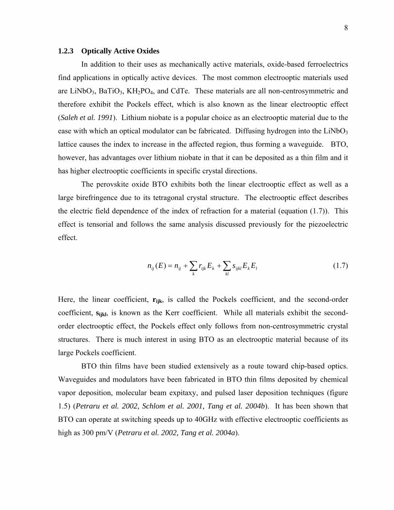
BTO thin films have been studied extensively as a route toward chip-based optics.
Waveguides and modulators have been fabricated in BTO thin films deposited by chemical
vapor deposition, molecular beam expitaxy, and pulsed laser deposition techniques (figure
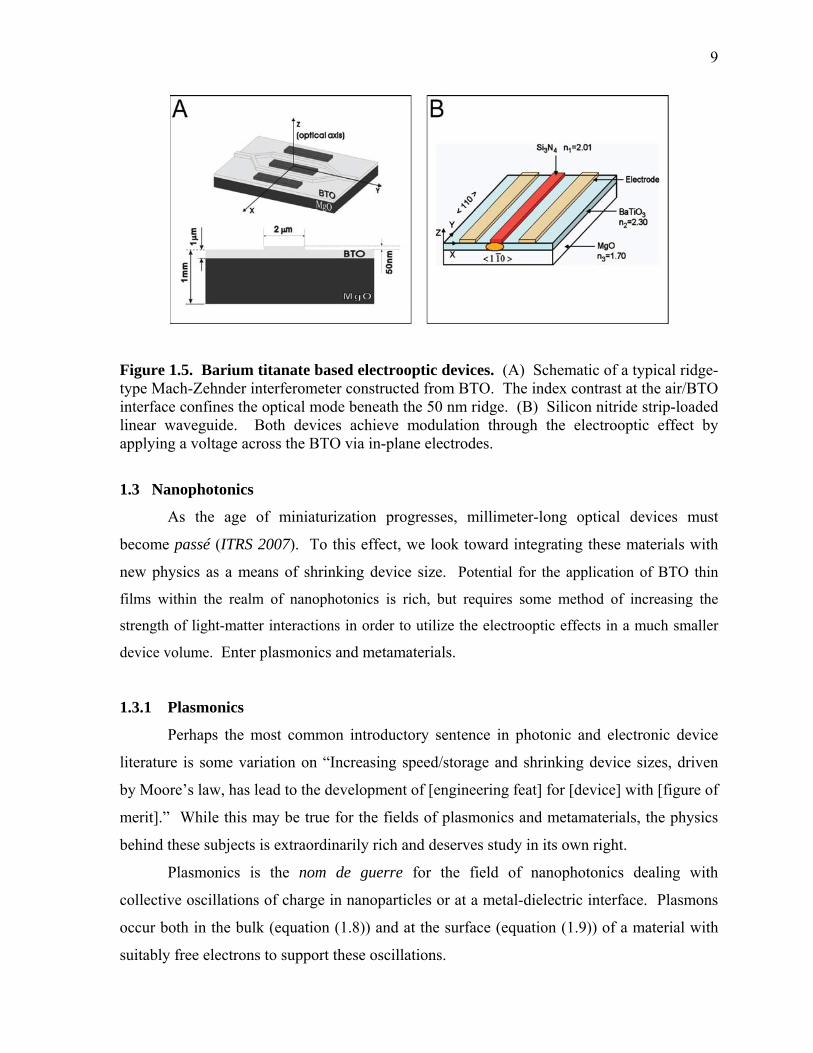
1.5) (Petraru et al. 2002, Schlom et al. 2001, Tang et al. 2004b). It has been shown that
BTO can operate at switching speeds up to 40GHz with effective electrooptic coefficients as
high as 300 pm/V (Petraru et al. 2002, Tang et al. 2004a).
9
Figure 1.5. Barium titanate based electrooptic devices. (A) Schematic of a typical ridge-type Mach-Zehnder interferometer constructed from BTO. The index contrast at the air/BTO interface confines the optical mode beneath the 50 nm ridge. (B) Silicon nitride strip-loaded linear waveguide. Both devices achieve modulation through the electrooptic effect by applying a voltage across the BTO via in-plane electrodes.
1.3 Nanophotonics
As the age of miniaturization progresses, millimeter-long optical devices must
become passé (ITRS 2007). To this effect, we look toward integrating these materials with
new physics as a means of shrinking device size. Potential for the application of BTO thin
films within the realm of nanophotonics is rich, but requires some method of increasing the
strength of light-matter interactions in order to utilize the electrooptic effects in a much smaller
device volume. Enter plasmonics and metamaterials.
1.3.1 Plasmonics
Perhaps the most common introductory sentence in photonic and electronic device
literature is some variation on “Increasing speed/storage and shrinking device sizes, driven
by Moore’s law, has lead to the development of [engineering feat] for [device] with [figure of
merit].” While this may be true for the fields of plasmonics and metamaterials, the physics
behind these subjects is extraordinarily rich and deserves study in its own right.
Plasmonics is the nom de guerre for the field of nanophotonics dealing with
collective oscillations of charge in nanoparticles or at a metal-dielectric interface. Plasmons
occur both in the bulk (equation (1.8)) and at the surface (equation (1.9)) of a material with
suitably free electrons to support these oscillations.
10
0
24
m
Nep (1.8)
d
psp
21 (1.9)
Here, p and sp are the bulk and surface plasmon frequencies, N is the density of electrons,
m is the electron mass, e the electron charge and 0 and d the permittivity of free space and
relative permittivity of the medium. Optical power can be coupled into plasmon modes
externally via electromagnetic waves. The fundamentally interesting property of surface
plasmons is the broad spectrum of frequencies possible depending on the wave vector. The
dispersion relation for surface plasmons lies to the right of the “light line” ( = ck), meaning
they have a longer wavevector than light with the same energy. Since surface plasmons have
a higher momentum than light, they remain bound to the surface during propagation. This
leads to a propagating mode with evanescent fields into both the metal and the dielectric as
described by (Raether 1988),
dm
dmsp kk
0 , (1.10)
where m and d are the dielectric functions of the metal and the dielectric, and k0 and ksp are
the free-space and surface plasmon wavevectors.
Plasmon oscillations can also be induced in localized geometries such as
nanoparticles, or nanoscale grooves and holes in metals. Electromagnetic waves can be used
to pump the free electrons in a metal nanoparticle. This leads to enhanced absorption at the
plasmon frequency of the metal because the energy is being coupled efficiently into this
mode. Plasmons can be coupled into surface modes using grating-like structures, or
launched from grooves or slits. There is a wealth of literature exploring this coupling via
gratings as well as enhanced transmission due to plasmon propagation through sub-
wavelength slits and holes (Ebbesen et al. 1998, Garcia-Vidal et al. 2003, Lalanne et al.

11
2005, Lezec et al. 2002, Lezec et al. 2004, Thio et al. 2001). This work uses plasmon-
mediated enhanced transmission from subwavelength slits to design plasmon interferometer
structures, as described in chapter 6.
Recently there has been increased interest in using optically active materials for
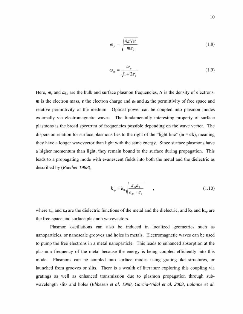
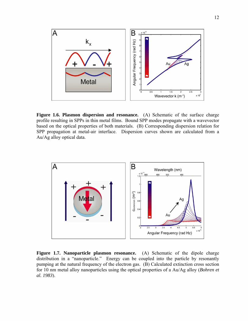
plasmonics and metamaterial applications (Pacifici et al. 2007). It has been found that
electromagnetic radiation can be coupled into these oscillations and propagate as a surface
plasmon polaritons (SPPs) at a metal-insulator interface (figure 1.6) (Barnes et al. 2003,
Dionne et al. 2005, Kretschmann et al. 1968). Metallic nanoparticles show analogous
behavior when resonantly pumped at their plasmon frequency, resulting in enhanced
absorption (figure 1.7) (Maier et al. 2003, Sweatlock et al. 2005, Wei et al. 2004).
12
Figure 1.6. Plasmon dispersion and resonance. (A) Schematic of the surface charge profile resulting in SPPs in thin metal films. Bound SPP modes propagate with a wavevector based on the optical properties of both materials. (B) Corresponding dispersion relation for SPP propagation at metal-air interface. Dispersion curves shown are calculated from a Au/Ag alloy optical data.
Figure 1.7. Nanoparticle plasmon resonance. (A) Schematic of the dipole charge distribution in a “nanoparticle.” Energy can be coupled into the particle by resonantly pumping at the natural frequency of the electron gas. (B) Calculated extinction cross section for 10 nm metal alloy nanoparticles using the optical properties of a Au/Ag alloy (Bohren et al. 1983).

13
Coupling EM radiation into SPP modes at a metal-dielectric interface using sub-
wavelength slits and grooves has been studied extensively (Ebbesen et al. 1998, Lezec et al.
2002, Lezec & Thio 2004). We are interested in coupling light into these modes at a metal-
oxide interface in order to shrink the SPP wavelength and increase the light-matter
interaction. Figure 1.8 shows schematically how the wavelength of a SPP changes in a
metal-insulator-metal structure. Incorporating optically active materials into these plasmonic
structures has led to tunable devices and has implications for future work on metal-insulator-
metal waveguides, transistor-like devices, and more vibrant optical display technologies.
Figure 1.8. Metal-insulator-metal plasmon waveguide. Schematic showing the SPP wavelength change in a metal-insulator-metal structure as the dimensions shrink. Light is very strongly confined in the thinnest section of the waveguide, propagating with a wavelength 15 times smaller than it would in free space. 1.3.2 Metamaterials
Metamaterials are distinguished from their cousins, “regular materials,” by the fact
that they are designed and fabricated from an array of subwavelength metal structures in a
dielectric medium. These novel structures, or composite materials, have electromagnetic
response functions not physically realizable in nature. The metal structures are typically
notched rings, so-called split-ring resonators (SRRs), with physical dimensions much smaller
than the wavelength of interest. Each SRR acts as nanoscale R-L-C circuit, and the
collective response of arrays of these rings is equivalent to that of a material with a new
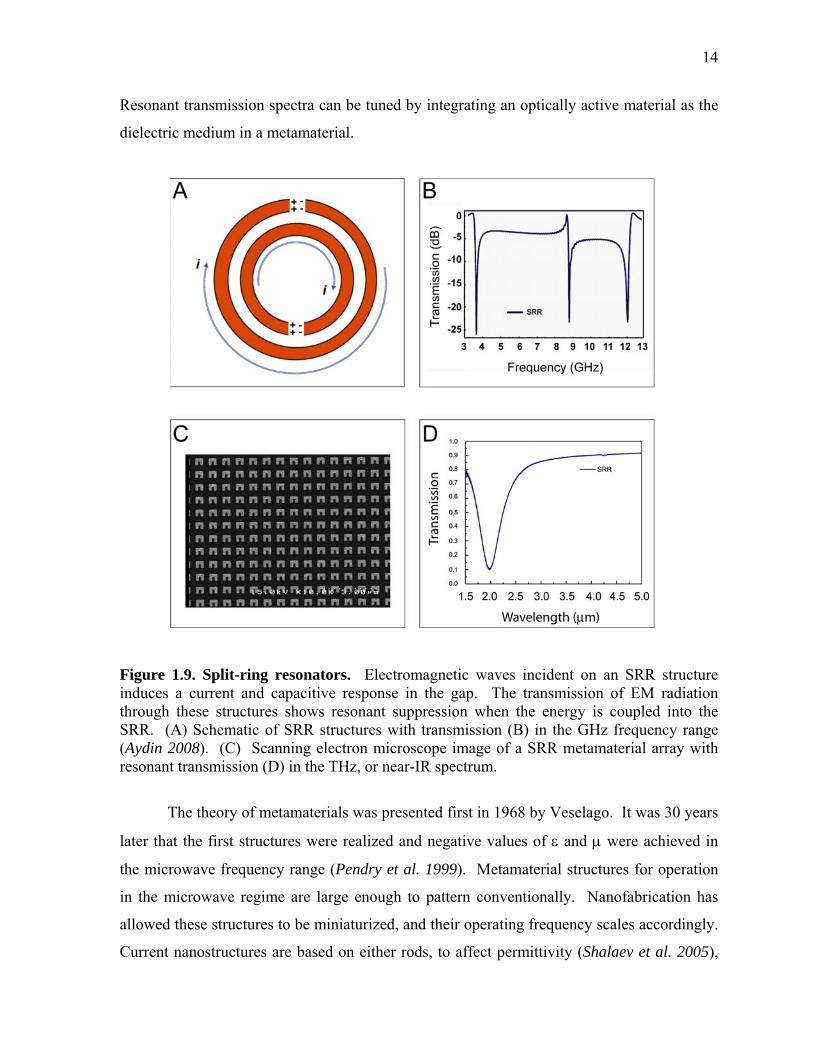
magnetic permeability, , or electric permittivity, and thus new transmission and reflection
properties (figure 1.9) (Smith et al. 2000, Veselago 1968). Through intelligent design, these
materials can be made to exhibit negative values of either , , or both simultaneously.
14
Resonant transmission spectra can be tuned by integrating an optically active material as the
dielectric medium in a metamaterial.
Figure 1.9. Split-ring resonators. Electromagnetic waves incident on an SRR structure induces a current and capacitive response in the gap. The transmission of EM radiation through these structures shows resonant suppression when the energy is coupled into the SRR. (A) Schematic of SRR structures with transmission (B) in the GHz frequency range (Aydin 2008). (C) Scanning electron microscope image of a SRR metamaterial array with resonant transmission (D) in the THz, or near-IR spectrum.
The theory of metamaterials was presented first in 1968 by Veselago. It was 30 years
later that the first structures were realized and negative values of and were achieved in
the microwave frequency range (Pendry et al. 1999). Metamaterial structures for operation
in the microwave regime are large enough to pattern conventionally. Nanofabrication has
allowed these structures to be miniaturized, and their operating frequency scales accordingly.
Current nanostructures are based on either rods, to affect permittivity (Shalaev et al. 2005),
15
or split-ring resonators, to affect permeability (Linden et al. 2004). Nanostructured
metamaterials have their resonant properties in the mid- and near-infrared spectrum. The
first example of an active metamaterial in the THz frequency band was shown by Chen et al.
and utilized the depletion region in a metal-semiconductor junction to change the gap length
in an array of SRRs (Chen et al. 2006) and the same group showed this effect in SRRs on
silicon by photoexcitation of charge carriers (Chen et al. 2008). We will discuss simulations
and experiments for active metamaterials, based on the metal-insulator transition in VO2.
1.4 Thesis Scope
The work presented in this thesis can be divided into three parts: developing active
oxide materials as thin films, designing optical devices based on these thin films, and
experimentally validating these devices. Initially, this research focused primarily on
mechanically active thin films based on BTO, and films were developed and characterized
with this in mind. Following the success of those endeavors, we saw an opportunity to utilize
oxide thin films to design active devices in the emerging fields of plasmonics and
metamaterials. Devices based on these effects were designed, modeled, fabricated, and
tested in this work. For the purposes of this thesis, we will discuss film growth,
characterization, and device applications in three separate sections.
1.4.1 Part I: Thin Film Deposition and Characterization Techniques
The section on film growth will cover the techniques used to deposit thin films of the
various oxide materials used in this thesis work. These materials include BTO, SRO, STO,
PTO and VO2. Deposition of these materials was carried out using either molecular beam
epitaxy (MBE) or pulsed laser deposition (PLD). Also included in this section is a
description of ion beam assisted deposition (IBAD) of MgO. IBAD is used to integrate
biaxially oriented thin films of complex oxides on arbitrary, smooth substrates.
Chapter 2 covers the background for the work presented here through an in-depth
look at ferroelectric thin film deposition and characterization techniques. A description of
the material deposition techniques will be given, with emphasis on those used to develop
oxide thin films. The three most prevalent characterization techniques used will be covered:
reflection high energy electron diffraction (RHEED), variable angle spectroscopic
ellipsometry (VASE), and piezoforce microscopy (PFM).
16
Chapter 3 provides a thorough description of the thin film materials grown, and the
quality of these films with respect to crystal structure, degree of epitaxy, orientation, and
phase. IBAD MgO deposited on amorphous silicon nitride, or any substrate with less than 5
nm RMS roughness, yields a biaxially oriented template on which any material lattice
matched to MgO can be grown. We will compare growth of BTO, PTO, SRO, STO, and
VO2 on IBAD MgO and bulk MgO, as well as other substrates. BTO is the flagship material
for this thesis and its growth via MBE and PLD will be discussed in depth. Similarly, PLD
was found to be the most versatile growth process and its role in deposition of BTO, SRO,
PTO, SRO, and VO2 will be highlighted.
1.4.2 Part II: Mechanical and Optical Characterization of Active Oxides
The results of extensive mechanical and optical characterization of thin films used in
this work are discussed in Part II of the thesis. Chapter 4 deals specifically with mechanical
characterization. The piezo- and ferroelectric properties of BTO were investigated for films
on bulk and IBAD MgO substrates. Piezoforce microscopy and nanoindentation was
performed on BTO thin films to study ferroelectric domain properties. Comparative PFM
studies were done on BTO grown on conductive layers of Pt, SRO, and lanthanum strontium
cobalt oxide (LSCO). Additionally, films were micromachined into cantilevers to investigate
domain switching as a means of mechanical beam bending.
Optical characterization of the films was carried out using variable angle
spectroscopic ellipsometry. Chapter 5 presents optical models used to fit VASE data and
extract the index of refraction and absorption as a function of wavelength over the range 300-
2200 nm for many of the materials discussed in this thesis. A parametric study of MBE BTO
growth is presented showing the effects of oxygen on the absorption characteristics of the
films. Two models are presented for PLD VO2 thin films, describing its index and
absorption in both the semiconducting and metallic phases.
1.4.3 Part III: Active Metal-Oxide Nanophotonics
Having developed and characterized thin films of active oxide materials, we turn our
attention to device applications in the final portion of the thesis. Mechanical applications,
specifically MEMS cantilevers and bridges, are the topic of previous thesis work. Here, we
17
present optical device applications for these active oxide thin films in the form of double-slit
plasmonic interferometers and optically active metamaterials.
Active oxide applications to SPP-mediated devices are covered in chapter 6.
Transmission from arrays of double-slit interferometers milled in Ag films on BTO is used to
investigate SPP propagation. Specifically, modulation of the SPP wavevector through
electrooptic changes in the BTO index of refraction will be discussed. Modulation was
achieved by applying a voltage across the BTO film via the silver top contact and a layer of
transparent, conductive, SRO under the film. Change in the transmission as a function of
voltage is attributed to a combination of domain switching and the electrooptic effects in
BTO.
This work continues in chapter 7 where we investigate, fabricate, and test active
metamaterials based on VO2. Metamaterial designs were engineered to take advantage of the
insulator-metal phase transition in VO2. Arrays of metal/VO2 hybrid-SRRs can have their
transmission spectra modified by electrically shorting the ring at the phase transition
temperature. We designed, simulated, fabricated, and experimentally verified active
metamaterials with resonant transmission peaks in the near-infrared range. The effects of
heating, applied voltage and optical switching of the VO2 thin films and SRR structures will
be discussed.
Chapter 8 investigates a combinatorial technique for bimetal alloy deposition with
regard to the optical properties of the metal alloy. Magnetron sputtering was used to
codeposit bimetal alloys of various metals including; Ag, Au, and Cu. The optical properties
as a function of alloy composition were measured using VASE. We found that the optical
properties changed smoothly from one pure element to the other. The optical data were used
to validate a new method for fitting the dielectric function using a genetic algorithm based on
Lorentz-Drude-Debye formalism.
18
Part I
Thin Film Deposition and Characterization Techniques
19
Chapter 2
Background
This chapter illuminates the relevant mechanical and optical material properties,
various deposition and characterization techniques used, and the applications toward the
fields of plasmonics and metamaterials to which this thesis, as a whole, aspires.
2.1 Deposition Techniques
There are numerous deposition techniques for thin film materials in the literature.
The choice of a deposition technique is often a trade-off between ease of processing and
material quality. Common processing techniques for oxides include: sol-gel, metal-organic
vapor deposition, MBE, and PLD. For the purposes of this thesis we will discuss the latter
two techniques, MBE and PLD. Prior to the discussion of growth techniques, we will
introduce IBAD MgO as a method for integration of biaxially oriented thin films.
2.1.1 Ion Beam Assisted Deposition of MgO
IBAD was first used by Yu et al. to grow biaxially oriented niobium films on
amorphous substrates. The technique uses an ion beam, impinging on the substrate, to
develop the texture of a material being deposited by physical vapor deposition. There are
two purported mechanisms to explain how IBAD develops the biaxial texture. The first
considers selective milling of the material being deposited contingent upon its orientation to
the ion beam (Bradley et al. 1986, Yu et al. 1985). The second relies on molecular dynamics
simulations to show that anisotropic, ion-induced, damage leads to grains of one dominant
orientation (Dong et al. 1998, Ressler et al. 1997).
Using the IBAD technique, biaxially oriented MgO has been deposited on silicon
nitride with less than 7° FWHM in-plane distribution and less than 4° FWHM out-of-plane
distribution (Brewer et al. 2002). Biaxially textured films have grains oriented with a narrow
distribution in-plane and out-of-plane and exhibit properties converging on those of a single
crystal. We used IBAD MgO templates to deposit biaxially oriented ferroelectric films on
silicon nitride and silicon dioxide to investigate crystal orientation effects on piezoresponse.
Deposition of both IBAD MgO and heteroepitaxial BTO takes place sequentially in the same

20
UHV chamber (figure 2.1). The IBAD MgO films fabricated using this system have been
used extensively in this work in addition to work previously published by El-Naggar and
Ruglovsky (El-Naggar 2006, Ruglovsky 2007). Specific characterization results for these
films will be discussed in chapter 3.
Figure 2.1. Ultra-high vacuum molecular beam epitaxy system. (A) UHV chamber equipped for IBAD MgO and MBE of complex oxides. (B) Chamber schematic showing the placement of the titanium sublimation pump, barium and lead effusion cells, e-beam MgO source, argon ion gun used for IBAD, RF oxygen plasma source and in situ RHEED.
2.1.2 Molecular Beam Epitaxy-MBE
Initial work on BTO deposition was carried out using an UHV chamber equipped for
MBE deposition of oxide materials. MBE uses high temperature effusion cells to
individually heat Ba, Pb, or Sr, creating a uniform flux of material toward the substrate. The
custom built MBE chamber is also equipped with a Ti sublimation pump (Varian Ti-Ball)
which is used as a Ti source (Theis et al. 1996). Each material source is operated by a
computer controlled pneumatic shutter using Labview software. Layer-by-layer deposition
takes place by shuttered growth in an oxygen ambient provided by a leak valve through a RF
plasma source. The RF plasma source generates reactive oxygen radicals which lead to
better film stoichiometry and lower optical absorption. A quartz crystal monitor is used to
21
measure flux rates and confirm stability prior to deposition. Once the source deposition rates
and substrate temperature are stable, the substrate shutter is retracted and the source-
shuttered growth begins. Previously, MBE has been used to grow thin films of BTO, STO,
and PTO (Schlom et al. 2001). They have demonstrated such effects as strain induced
lowering of the Curie temperature through substrate engineering (Choi et al. 2004).
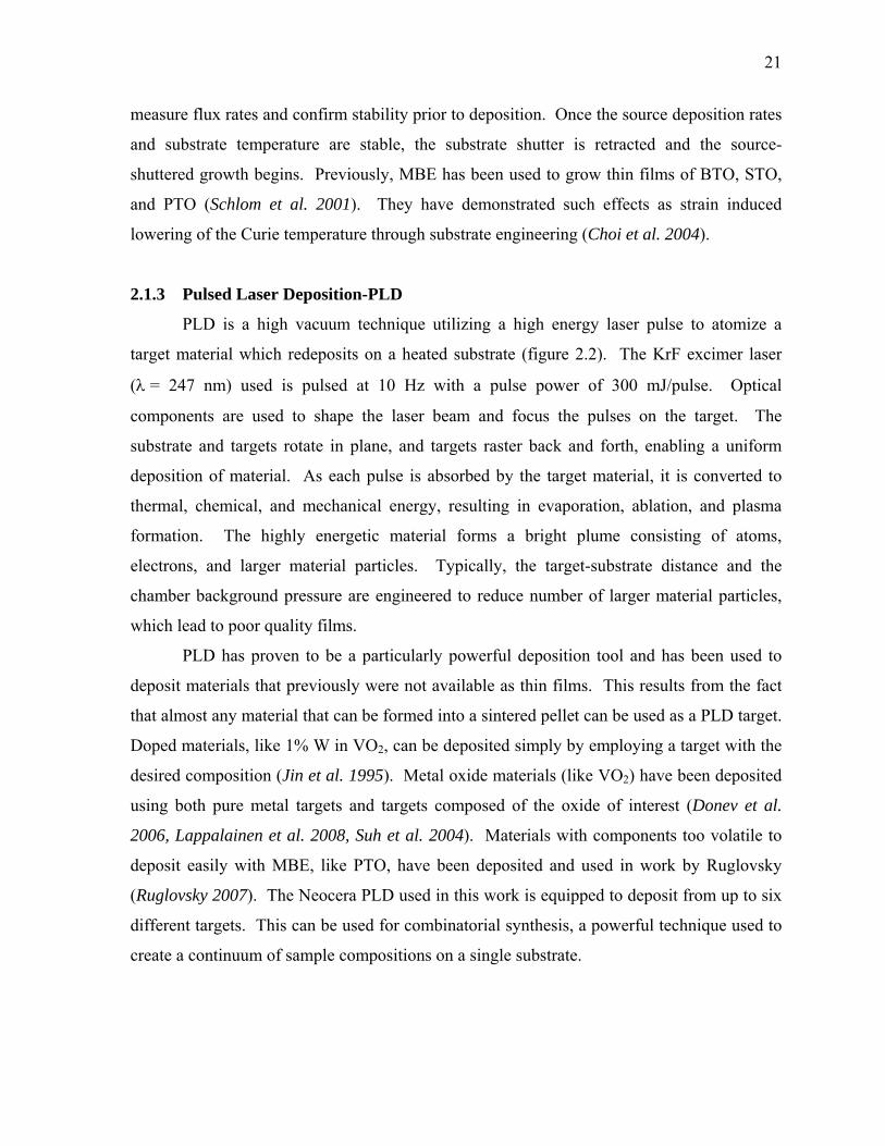
2.1.3 Pulsed Laser Deposition-PLD
PLD is a high vacuum technique utilizing a high energy laser pulse to atomize a
target material which redeposits on a heated substrate (figure 2.2). The KrF excimer laser
(= 247 nm) used is pulsed at 10 Hz with a pulse power of 300 mJ/pulse. Optical
components are used to shape the laser beam and focus the pulses on the target. The
substrate and targets rotate in plane, and targets raster back and forth, enabling a uniform
deposition of material. As each pulse is absorbed by the target material, it is converted to
thermal, chemical, and mechanical energy, resulting in evaporation, ablation, and plasma
formation. The highly energetic material forms a bright plume consisting of atoms,
electrons, and larger material particles. Typically, the target-substrate distance and the
chamber background pressure are engineered to reduce number of larger material particles,
which lead to poor quality films.
PLD has proven to be a particularly powerful deposition tool and has been used to
deposit materials that previously were not available as thin films. This results from the fact
that almost any material that can be formed into a sintered pellet can be used as a PLD target.
Doped materials, like 1% W in VO2, can be deposited simply by employing a target with the
desired composition (Jin et al. 1995). Metal oxide materials (like VO2) have been deposited
using both pure metal targets and targets composed of the oxide of interest (Donev et al.
2006, Lappalainen et al. 2008, Suh et al. 2004). Materials with components too volatile to
deposit easily with MBE, like PTO, have been deposited and used in work by Ruglovsky
(Ruglovsky 2007). The Neocera PLD used in this work is equipped to deposit from up to six
different targets. This can be used for combinatorial synthesis, a powerful technique used to
create a continuum of sample compositions on a single substrate.
22
Figure 2.2. Pulsed laser deposition system. (A) PLD schematic showing the relative placement of targets, substrate, and quartz laser port. (B) Example of energetic plume of material created with each laser pulse. (C) Neocera PLD system.
23
2.2 Characterization Techniques
In the beginning stages of thin film development, material properties are optimized by
changing process parameters with each sample growth. During this phase, each sample
requires extensive characterization to dictate the parameters of the next sample. It is
important to have a method for in situ characterization during growth. In this work we rely
heavily on in situ RHEED to characterize films. After growth, we use numerous ex-situ
characterization techniques such as x-ray diffraction (XRD), variable angle spectroscopic
ellipsometry (VASE), and piezoforce response microscopy (PFM) to examine thin film
quality and dictate the next step in optimization.
2.2.1 Reflection High-Energy Electron Diffraction-RHEED
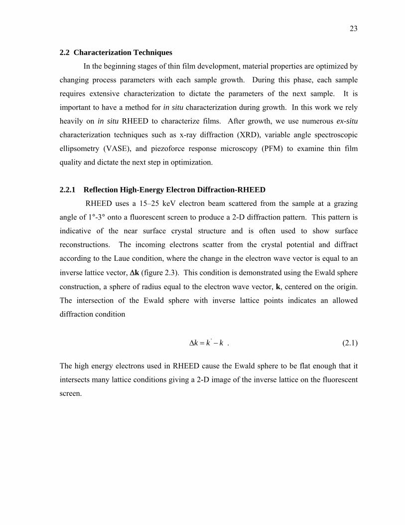
RHEED uses a 15–25 keV electron beam scattered from the sample at a grazing
angle of 1°-3° onto a fluorescent screen to produce a 2-D diffraction pattern. This pattern is
indicative of the near surface crystal structure and is often used to show surface
reconstructions. The incoming electrons scatter from the crystal potential and diffract
according to the Laue condition, where the change in the electron wave vector is equal to an
inverse lattice vector, k (figure 2.3). This condition is demonstrated using the Ewald sphere
construction, a sphere of radius equal to the electron wave vector, k, centered on the origin.
The intersection of the Ewald sphere with inverse lattice points indicates an allowed
diffraction condition
kkk ' . (2.1)
The high energy electrons used in RHEED cause the Ewald sphere to be flat enough that it
intersects many lattice conditions giving a 2-D image of the inverse lattice on the fluorescent
screen.
24
Figure 2.3. Reflection high-energy electron diffraction. (A) Schematic of in situ RHEED showing how the Laue condition results in diffraction spots on the luminescent screen. (B) Ewald construction showing the diffraction conditions that result in bright spots in the RHEED pattern.
RHEED patterns are generated by electron scattering from the crystal lattice potential.
It is possible, therefore, to calculate the RHEED pattern by solving the Schrödinger equation
for the interaction of electrons with the crystal potential V(r)
022 rkrVr . (2.6)
Using a semi-infinite crystal scattering potential leads to simple Bloch function solutions of
the form
k
k rikrr exp . (2.7)
The solutions to the Bloch expansion are taken over all inverse lattice vectors k to satisfy the
Laue condition for an electron to scatter into a different mode. Solving the dynamical
scattering problem can be done computationally and leads to information about the RHEED
spot intensities and shapes. A wealth of information regarding film crystallinity, grain size,
surface reconstructions, and surface morphology is contained in RHEED spot shapes and
intensities.
Kinematical simulations can be used to reconstruct RHEED spots for a given
material, angle of incidence, grain size, and grain orientation distribution. From these
simulations, a qualitative understanding of RHEED spot shape can be developed.
25
Simulations show that RHEED spot widths are inversely proportional to grain size and height
is inversely proportional to electron penetration depth. The out-of-plane grain distribution is
proportional to the width of the central diffraction spots. In-plane-orientation requires
analysis, at various in-plane angles, of the spot intensities, a rocking curve. This analysis,
developed by Brewer et al., has been used to characterize IBAD MgO growth and as a
heuristic to qualitatively characterize other thin films throughout this work.
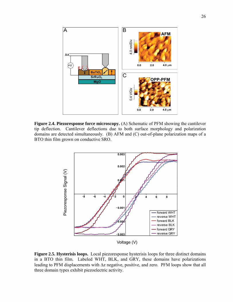
2.2.2 Piezoresponse Force Microscopy-PFM
There are a variety of powerful scanning probe techniques based on deflection of a
cantilever tip from the sample surface. Using this geometry with some modification, the
surface roughness, electrical and mechanical characteristics can be investigated. One such
specialized use is PFM (figure 2.4). PFM uses an atomic force microscopy (AFM) setup
equipped with conducting tips to apply an AC voltage in the 1–5 V range to the sample
surface. A lock-in amplifier is used to detect the deflection due to the local piezoelectric
response. Grain-by-grain response is monitored using the conductive AFM tip to scan the
surface. This is contingent upon the film having a suitable backside electrode, meaning all
samples must be grown on conductive substrates. Local piezoelectric hysteresis loops may
be obtained by sweeping a DC bias across the sample and recording the piezoresponse
(figure 2.5).
26
Figure 2.4. Piezoresponse force microscopy. (A) Schematic of PFM showing the cantilever tip deflection. Cantilever deflections due to both surface morphology and polarization domains are detected simultaneously. (B) AFM and (C) out-of-plane polarization maps of a BTO thin film grown on conductive SRO.
Figure 2.5. Hysterisis loops. Local piezoresponse hysterisis loops for three distinct domains in a BTO thin film. Labeled WHT, BLK, and GRY, these domains have polarizations leading to PFM displacements with z negative, positive, and zero. PFM loops show that all three domain types exhibit piezoelectric activity.
27
In PFM, the signal is recorded as Acos(), where A is the amplitude of the first
harmonic signal, which provides information about the magnitude of the piezo-coefficient,
d33, in the measured z-direction, and is the phase shift between the AC voltage applied
through the tip and the piezoresponse which determines the direction of polarization.
Equation (2.8) relates this signal to the field induced strain.
acaccdclever
VdVVVkdz
dCA 33
1cos
(2.8)
Throughout this work, when appropriate, we use AFM and PFM to confirm the domain
activity in thin ferroelectric films. AFM is used extensively to compare surface morphology
from sample to sample, especially for optical applications where surface scattering can be an
issue. PFM also determines the domain size, polarization orientation, and switching fields.
2.2.3 Variable Angle Spectroscopic Ellipsometry–VASE
Ellipsometry is an optical characterization technique for thin film materials that uses
linearly polarized light scattered from the sample and collected through a rotating polarizer.
The incident light interacts with the film which imparts both phase and rotation to the
scattered signal. The nature of this interaction depends on the complex index of refraction of
the material, Ñ =n + i. The complex index, Ñ, is comprised of the real index of refraction,
n, and the extinction coefficient, . The real part of the index is related to the phase velocity
of light in the material while the extinction coefficient determines how quickly the light will
be absorbed by the material.

28
Figure 2.6. Ellipsometry. (A) Linearly polarized light is scattered from the sample and detected through a polarizer, and are the measured quantities. (B) and are used to extract n and from each layer with the application of a suitable optical model.
Ellipsometry examines both the reflection and transmission properties of the sample
of interest. Reflections from each interface in a material stack are governed by the Fresnel
equations and the total reflection coefficient can be derived for s- and p-polarizations as
2exp1
2exp
2312
2312
irr
irrR
pp
ppp
,
2exp1
2exp
2312
2312
irr
irrR
ss
sss
, (2.9)
where rab are the Fresnel reflection coefficients from the interface between a and b, and
22
~
cos2
Nd
. (2.10)
Here, d is the layer thickness, the wavelength of light, Ñ2 is the complex index of the layer,
and is the phase shift due to the layer. Equation (2.9) is explicit for a three-layer stack but
can be generalized to an arbitrary number of material layers.
These represent the total reflection coefficients for a single film, two interfaces and
three materials; denoted 1, 2, and 3. Using the ratio of these reflectance coefficients, Rp and
Rs, and including the possibility of a phase shift from each interface leads to the general
equations for ellipsometry, and as
29
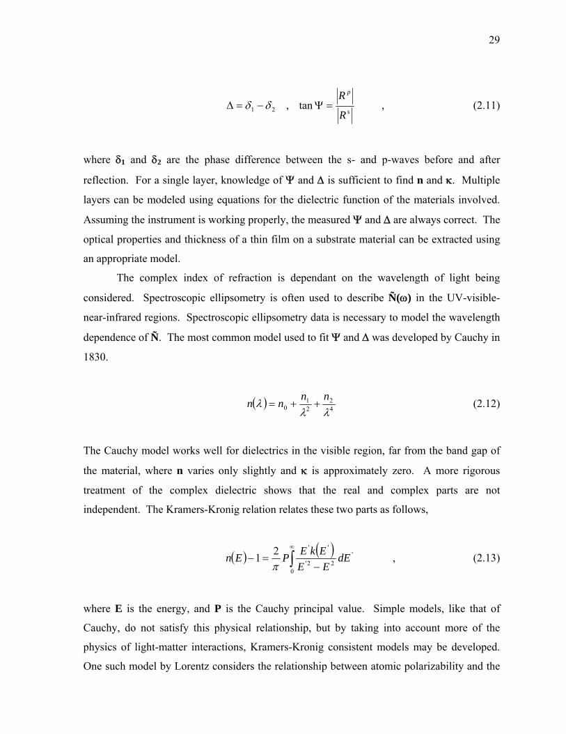
21 , s
p
R
Rtan , (2.11)
where 1 and 2 are the phase difference between the s- and p-waves before and after
reflection. For a single layer, knowledge of and is sufficient to find n and . Multiple
layers can be modeled using equations for the dielectric function of the materials involved.
Assuming the instrument is working properly, the measured and are always correct. The
optical properties and thickness of a thin film on a substrate material can be extracted using
an appropriate model.
The complex index of refraction is dependant on the wavelength of light being
considered. Spectroscopic ellipsometry is often used to describe Ñ() in the UV-visible-
near-infrared regions. Spectroscopic ellipsometry data is necessary to model the wavelength
dependence of Ñ. The most common model used to fit and was developed by Cauchy in
1830.
42
21
0
nnnn (2.12)
The Cauchy model works well for dielectrics in the visible region, far from the band gap of
the material, where n varies only slightly and is approximately zero. A more rigorous
treatment of the complex dielectric shows that the real and complex parts are not
independent. The Kramers-Kronig relation relates these two parts as follows,
0
'22'
''21 dE
EE
EkEPEn
, (2.13)
where E is the energy, and P is the Cauchy principal value. Simple models, like that of
Cauchy, do not satisfy this physical relationship, but by taking into account more of the
physics of light-matter interactions, Kramers-Kronig consistent models may be developed.
One such model by Lorentz considers the relationship between atomic polarizability and the
30
nature of electromagnetic radiation to define the dielectric function in terms of multiple
oscillator functions. In terms of 1 and 2, the Lorentz formulation reduces to
k kk
k
i
N
m
e
22
2~ 41 , (2.14)
with 2~~
N , e is the magnitude of the electronic charge, the damping, Nk is the density of
oscillators in the model, m the electronic mass, k is the resonant frequency in the absence of
damping and the pumping frequency. Variations on the Lorentz oscillator function are
used throughout this thesis to model dielectric functions and extract n and . Knowledge of
Ñ() for the thin film materials used here is necessary to design the optical devices.
2.3 Conclusions
MBE and PLD were used extensively in this thesis work to develop oxide thin films
for mechanical and optical applications. MBE offers a precise, high quality technique for
thin film deposition. MBE, however, requires UHV conditions, and deposition is very slow,
making initial investigations prohibitively long. PLD is a faster deposition technique which
only requires that a sintered or pure elemental target can be made of the material. Rapid,
accurate characterization of thin films is necessary during the initial stages of deposition.
RHEED and XRD are the two best techniques and should be applied liberally.
31
Chapter 3
Oxide Thin Film Growth Techniques
The intent of this chapter is to present work done to develop deposition techniques for
thin films of various oxide materials. These films were initially intended as a means for
investigating domain switching in ferroelectrics for high work per volume ferroelectric
MEMS. As such, they were designed to be integrated with Si CMOS processing. Integration
with Si relies heavily on IBAD MgO as a template for growth of biaxially textured oxides.
We will begin, therefore, by discussing IBAD MgO films, followed by MBE of BTO.
Following work on MBE growth, we use PLD to optimize growth of SRO thin films, to be
used as a lattice matched conductive oxide electrode in device designs. Film stacks of BTO
on SRO on IBAD MgO on amorphous Si3N4 on Si represent the successful integration of
active oxide ferroelectric materials for mechanical and optical applications. Finally, the
deposition and optimization of films of VO2, via PLD, for optical metamaterial applications
is discussed.
3.1 Ion Beam Assisted Deposition—MgO
IBAD films were deposited in an UHV chamber using an e-beam evaporator to
deposit MgO onto amorphous Si3N4 substrates oriented 45° to an Ar ion source. We use a
linear, 4-pocket, Temescal e-beam evaporator. The e-beam evaporator is housed separately
from the main UHV chamber, approximately 36 inches from the substrate. The copper
crucibles hold 5 cm3 of MgO. The e-beam is created via a hot filament adjacent to the
crucible and focused onto the material by two magnets. The filament current is controlled
through a high voltage power supply and the housing is water cooled. A quartz crystal
monitor is used to measure the deposition rate of the MgO. The minimum deposition rate to
achieve biaxially textured MgO films is 1.5 Å/sec, and the optimal rate, with regard to
orientation and grain size, is 2.0 Å/sec.
The IBAD process takes place at room temperature with 1.0 X 10⁻⁴ Torr background
Ar pressure to facilitate the ion beam. Ar ions are supplied using a Kauffman ion source. Ar
is supplied via a leak valve through the Kauffman source and ionized between two plates
held at high voltage. The Ar ions are accelerated toward the substrate due to a negatively
32
biased mesh at the base of the gun. A Faraday cup is used to calibrate the flux of the
incoming ions. The optimum ion current is 13.0 X 10⁻⁶ amps for the deposition parameters
reported here.
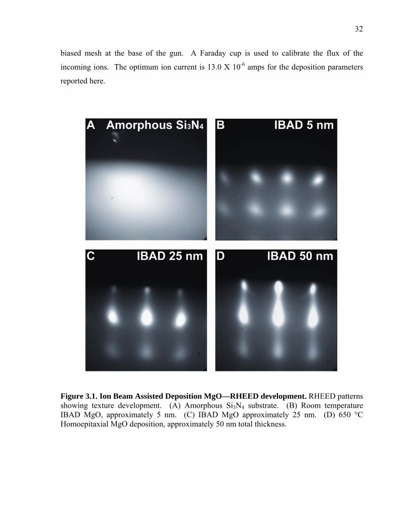
Figure 3.1. Ion Beam Assisted Deposition MgO—RHEED development. RHEED patterns showing texture development. (A) Amorphous Si3N4 substrate. (B) Room temperature IBAD MgO, approximately 5 nm. (C) IBAD MgO approximately 25 nm. (D) 650 °C Homoepitaxial MgO deposition, approximately 50 nm total thickness.
33
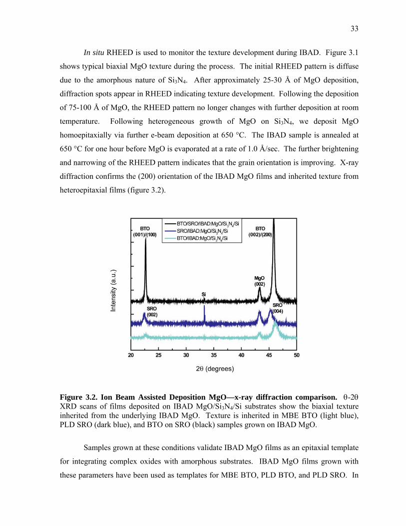
In situ RHEED is used to monitor the texture development during IBAD. Figure 3.1
shows typical biaxial MgO texture during the process. The initial RHEED pattern is diffuse
due to the amorphous nature of Si3N4. After approximately 25-30 Å of MgO deposition,
diffraction spots appear in RHEED indicating texture development. Following the deposition
of 75-100 Å of MgO, the RHEED pattern no longer changes with further deposition at room
temperature. Following heterogeneous growth of MgO on Si3N4, we deposit MgO
homoepitaxially via further e-beam deposition at 650 °C. The IBAD sample is annealed at
650 °C for one hour before MgO is evaporated at a rate of 1.0 Å/sec. The further brightening
and narrowing of the RHEED pattern indicates that the grain orientation is improving. X-ray
diffraction confirms the (200) orientation of the IBAD MgO films and inherited texture from
heteroepitaxial films (figure 3.2).
Figure 3.2. Ion Beam Assisted Deposition MgO—x-ray diffraction comparison. -2 XRD scans of films deposited on IBAD MgO/Si3N4/Si substrates show the biaxial texture inherited from the underlying IBAD MgO. Texture is inherited in MBE BTO (light blue), PLD SRO (dark blue), and BTO on SRO (black) samples grown on IBAD MgO.
Samples grown at these conditions validate IBAD MgO films as an epitaxial template
for integrating complex oxides with amorphous substrates. IBAD MgO films grown with
these parameters have been used as templates for MBE BTO, PLD BTO, and PLD SRO. In
34
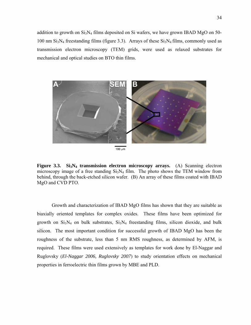
addition to growth on Si3N4 films deposited on Si wafers, we have grown IBAD MgO on 50-
100 nm Si3N4 freestanding films (figure 3.3). Arrays of these Si3N4 films, commonly used as
transmission electron microscopy (TEM) grids, were used as relaxed substrates for
mechanical and optical studies on BTO thin films.
Figure 3.3. Si3N4 transmission electron microscopy arrays. (A) Scanning electron microscopy image of a free standing Si3N4 film. The photo shows the TEM window from behind, through the back-etched silicon wafer. (B) An array of these films coated with IBAD MgO and CVD PTO.
Growth and characterization of IBAD MgO films has shown that they are suitable as
biaxially oriented templates for complex oxides. These films have been optimized for
growth on Si3N4 on bulk substrates, Si3N4 freestanding films, silicon dioxide, and bulk
silicon. The most important condition for successful growth of IBAD MgO has been the
roughness of the substrate, less than 5 nm RMS roughness, as determined by AFM, is
required. These films were used extensively as templates for work done by El-Naggar and
Ruglovsky (El-Naggar 2006, Ruglovsky 2007) to study orientation effects on mechanical
properties in ferroelectric thin films grown by MBE and PLD.
35
3.2 MBE BTO
MBE of BTO is carried out in the UHV chamber previously discussed for IBAD
MgO. This allows for monolithic deposition without breaking vacuum. The base chamber
pressure is 1 X 10⁻⁸ Torr with a background comprised entirely of oxygen supplied from a
leak valve attached to a RF plasma source. The chamber is equipped with two Knudsen
effusion cell sources, elemental Ba and Pb. These k-cells are small crucibles filled with a
pure element that is resistively heated until it sublimes at a reasonable rate. Ti is supplied
from a Varian Ti-Ball sublimation pump.
Traditionally, the elemental flux is calibrated using a quartz crystal monitor, atomic
emission spectroscopy, or other analysis. The information is then fed back to a program to
control deposition. This is not the case for titanate-based ferroelectrics due to the extreme
temperature of the Ti source. The quartz crystal monitor cannot be used to calibrate the
titanium flux because the radiative heating raises the temperature higher than the monitor can
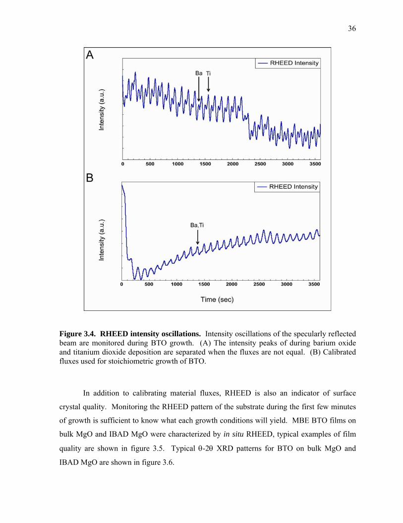
operate at. It was determined that RHEED oscillations could be used to calibrate growth
(figure 3.4).
In situ RHEED oscillations were used to calibrate the flux ratios for Ba and Ti. As
atoms are deposited on a flat surface the electron beam begins to scatter and the RHEED spot
loses intensity. This continues until the coverage is 50%, at which point the intensity
recovers. The intensity of the specular reflection spot is monitored with a CCD camera and
software provided by K-Space Associates. Source temperatures were calibrated using this
technique to yield equivalent flux rates. Subsequently, a source shuttering program was
written in Labview, and calibrated with RHEED, to optimize the flux and improve film
stoichiometry. Using these calibrated flux ratios, BTO thin films were deposited on bulk
MgO and IBAD MgO substrates. Deposition takes place at 650 °C with 1.5 X 10⁻⁵ Torr
background oxygen pressure. Oxygen was supplied through an RF plasma source operating
at 300 Watts. Plasma generated oxygen radicals lead to better oxygen stoichiometry and
hence, much higher optical quality BTO films, to be discussed in chapter 5.
36
Figure 3.4. RHEED intensity oscillations. Intensity oscillations of the specularly reflected beam are monitored during BTO growth. (A) The intensity peaks of during barium oxide and titanium dioxide deposition are separated when the fluxes are not equal. (B) Calibrated fluxes used for stoichiometric growth of BTO.
In addition to calibrating material fluxes, RHEED is also an indicator of surface
crystal quality. Monitoring the RHEED pattern of the substrate during the first few minutes
of growth is sufficient to know what each growth conditions will yield. MBE BTO films on
bulk MgO and IBAD MgO were characterized by in situ RHEED, typical examples of film
quality are shown in figure 3.5. Typical -2 XRD patterns for BTO on bulk MgO and
IBAD MgO are shown in figure 3.6.
37
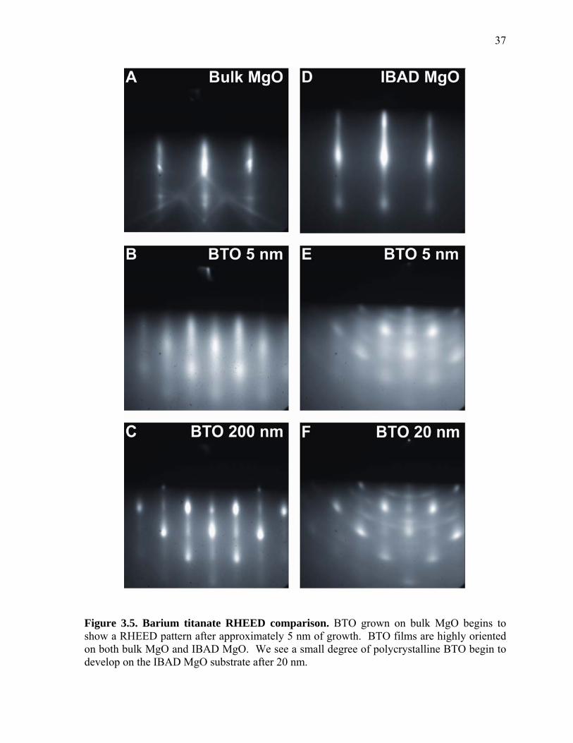
Figure 3.5. Barium titanate RHEED comparison. BTO grown on bulk MgO begins to show a RHEED pattern after approximately 5 nm of growth. BTO films are highly oriented on both bulk MgO and IBAD MgO. We see a small degree of polycrystalline BTO begin to develop on the IBAD MgO substrate after 20 nm.
38
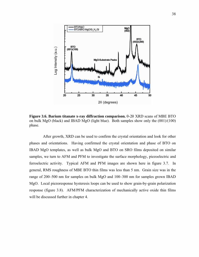
Figure 3.6. Barium titanate x-ray diffraction comparison. -2 XRD scans of MBE BTO on bulk MgO (black) and IBAD MgO (light blue). Both samples show only the (001)/(100) phase.
After growth, XRD can be used to confirm the crystal orientation and look for other
phases and orientations. Having confirmed the crystal orientation and phase of BTO on
IBAD MgO templates, as well as bulk MgO and BTO on SRO films deposited on similar
samples, we turn to AFM and PFM to investigate the surface morphology, piezoelectric and
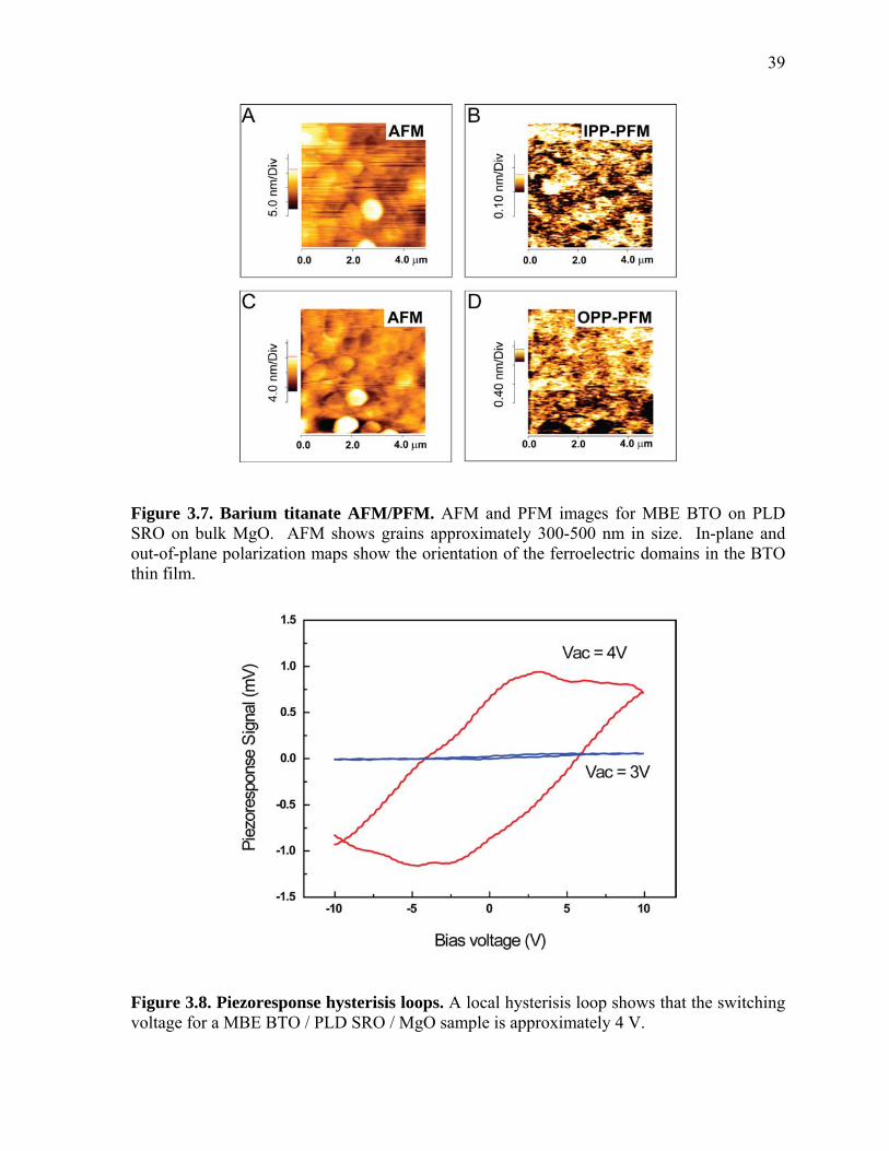
ferroelectric activity. Typical AFM and PFM images are shown here in figure 3.7. In
general, RMS roughness of MBE BTO thin films was less than 5 nm. Grain size was in the
range of 200–500 nm for samples on bulk MgO and 100–300 nm for samples grown IBAD
MgO. Local piezoresponse hysteresis loops can be used to show grain-by-grain polarization
response (figure 3.8). AFM/PFM characterization of mechanically active oxide thin films
will be discussed further in chapter 4.
39
Figure 3.7. Barium titanate AFM/PFM. AFM and PFM images for MBE BTO on PLD SRO on bulk MgO. AFM shows grains approximately 300-500 nm in size. In-plane and out-of-plane polarization maps show the orientation of the ferroelectric domains in the BTO thin film.
Figure 3.8. Piezoresponse hysterisis loops. A local hysterisis loop shows that the switching voltage for a MBE BTO / PLD SRO / MgO sample is approximately 4 V.
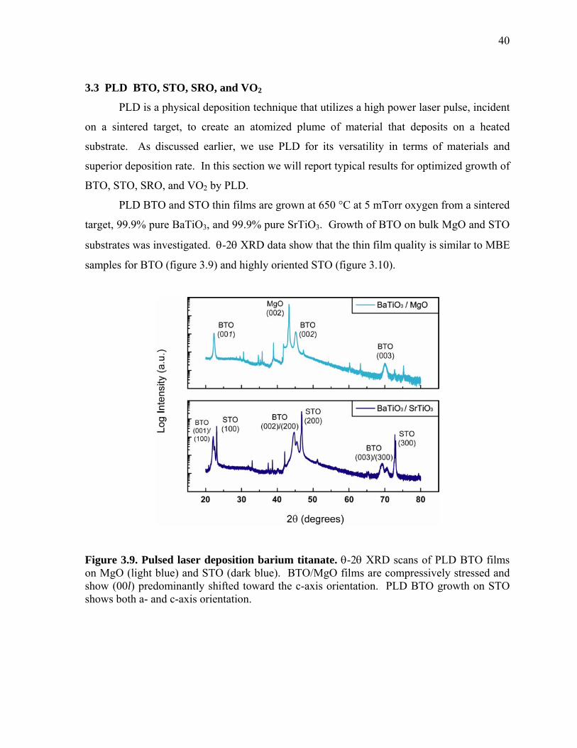
40
3.3 PLD BTO, STO, SRO, and VO2
PLD is a physical deposition technique that utilizes a high power laser pulse, incident
on a sintered target, to create an atomized plume of material that deposits on a heated
substrate. As discussed earlier, we use PLD for its versatility in terms of materials and
superior deposition rate. In this section we will report typical results for optimized growth of
BTO, STO, SRO, and VO2 by PLD.
PLD BTO and STO thin films are grown at 650 °C at 5 mTorr oxygen from a sintered
target, 99.9% pure BaTiO3, and 99.9% pure SrTiO3. Growth of BTO on bulk MgO and STO
substrates was investigated. -2 XRD data show that the thin film quality is similar to MBE
samples for BTO (figure 3.9) and highly oriented STO (figure 3.10).
Figure 3.9. Pulsed laser deposition barium titanate. -2 XRD scans of PLD BTO films on MgO (light blue) and STO (dark blue). BTO/MgO films are compressively stressed and show (00l) predominantly shifted toward the c-axis orientation. PLD BTO growth on STO shows both a- and c-axis orientation.
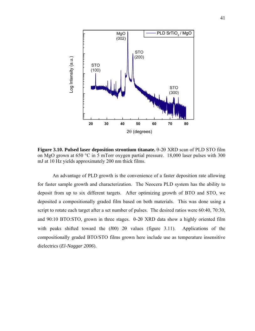
41
Figure 3.10. Pulsed laser deposition strontium titanate. -2 XRD scan of PLD STO film on MgO grown at 650 °C in 5 mTorr oxygen partial pressure. 18,000 laser pulses with 300 mJ at 10 Hz yields approximately 200 nm thick films.
An advantage of PLD growth is the convenience of a faster deposition rate allowing
for faster sample growth and characterization. The Neocera PLD system has the ability to
deposit from up to six different targets. After optimizing growth of BTO and STO, we
deposited a compositionally graded film based on both materials. This was done using a
script to rotate each target after a set number of pulses. The desired ratios were 60:40, 70:30,
and 90:10 BTO:STO, grown in three stages. -2 XRD data show a highly oriented film
with peaks shifted toward the (l00) 2 values (figure 3.11). Applications of the
compositionally graded BTO/STO films grown here include use as temperature insensitive
dielectrics (El-Naggar 2006).
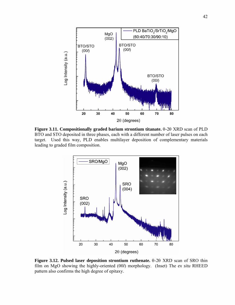
42
Figure 3.11. Compositionally graded barium strontium titanate. -2 XRD scan of PLD BTO and STO deposited in three phases, each with a different number of laser pulses on each target. Used this way, PLD enables multilayer deposition of complementary materials leading to graded film composition.
Figure 3.12. Pulsed laser deposition strontium ruthenate. -2 XRD scan of SRO thin film on MgO showing the highly-oriented (00l) morphology. (Inset) The ex situ RHEED pattern also confirms the high degree of epitaxy.
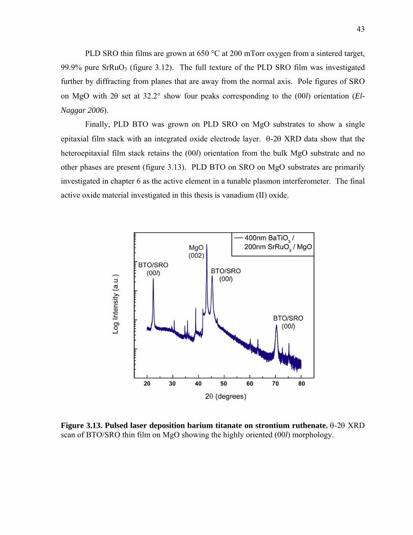
43
PLD SRO thin films are grown at 650 °C at 200 mTorr oxygen from a sintered target,
99.9% pure SrRuO3 (figure 3.12). The full texture of the PLD SRO film was investigated
further by diffracting from planes that are away from the normal axis. Pole figures of SRO
on MgO with 2 set at 32.2° show four peaks corresponding to the (00l) orientation (El-
Naggar 2006).
Finally, PLD BTO was grown on PLD SRO on MgO substrates to show a single
epitaxial film stack with an integrated oxide electrode layer. -2 XRD data show that the
heteroepitaxial film stack retains the (00l) orientation from the bulk MgO substrate and no
other phases are present (figure 3.13). PLD BTO on SRO on MgO substrates are primarily
investigated in chapter 6 as the active element in a tunable plasmon interferometer. The final
active oxide material investigated in this thesis is vanadium (II) oxide.
Figure 3.13. Pulsed laser deposition barium titanate on strontium ruthenate. -2 XRD scan of BTO/SRO thin film on MgO showing the highly oriented (00l) morphology.
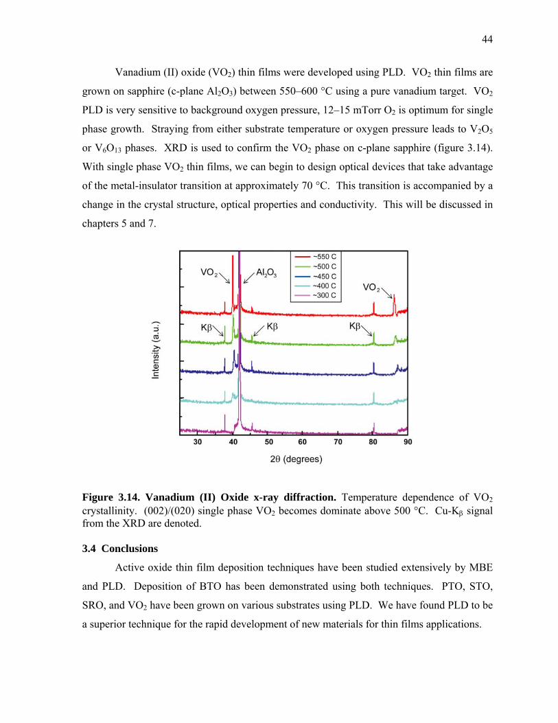
44
Vanadium (II) oxide (VO2) thin films were developed using PLD. VO2 thin films are
grown on sapphire (c-plane Al2O3) between 550–600 °C using a pure vanadium target. VO2
PLD is very sensitive to background oxygen pressure, 12–15 mTorr O2 is optimum for single
phase growth. Straying from either substrate temperature or oxygen pressure leads to V2O5
or V6O13 phases. XRD is used to confirm the VO2 phase on c-plane sapphire (figure 3.14).
With single phase VO2 thin films, we can begin to design optical devices that take advantage
of the metal-insulator transition at approximately 70 °C. This transition is accompanied by a
change in the crystal structure, optical properties and conductivity. This will be discussed in
chapters 5 and 7.
Figure 3.14. Vanadium (II) Oxide x-ray diffraction. Temperature dependence of VO2 crystallinity. (002)/(020) single phase VO2 becomes dominate above 500 °C. Cu-K signal from the XRD are denoted. 3.4 Conclusions
Active oxide thin film deposition techniques have been studied extensively by MBE
and PLD. Deposition of BTO has been demonstrated using both techniques. PTO, STO,
SRO, and VO2 have been grown on various substrates using PLD. We have found PLD to be
a superior technique for the rapid development of new materials for thin films applications.

45
Part II
Mechanical and Optical Characterization of Active Oxides
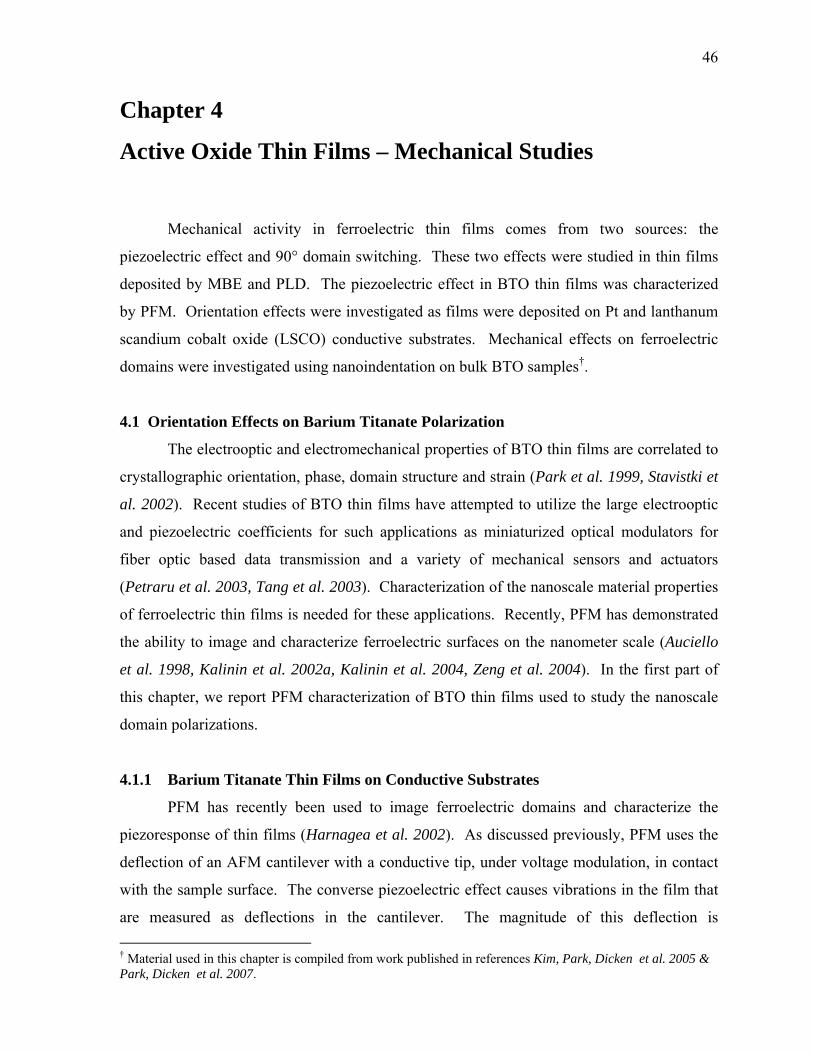
46
Chapter 4
Active Oxide Thin Films – Mechanical Studies
Mechanical activity in ferroelectric thin films comes from two sources: the
piezoelectric effect and 90° domain switching. These two effects were studied in thin films
deposited by MBE and PLD. The piezoelectric effect in BTO thin films was characterized
by PFM. Orientation effects were investigated as films were deposited on Pt and lanthanum
scandium cobalt oxide (LSCO) conductive substrates. Mechanical effects on ferroelectric
domains were investigated using nanoindentation on bulk BTO samples†.
4.1 Orientation Effects on Barium Titanate Polarization
The electrooptic and electromechanical properties of BTO thin films are correlated to
crystallographic orientation, phase, domain structure and strain (Park et al. 1999, Stavistki et
al. 2002). Recent studies of BTO thin films have attempted to utilize the large electrooptic
and piezoelectric coefficients for such applications as miniaturized optical modulators for
fiber optic based data transmission and a variety of mechanical sensors and actuators
(Petraru et al. 2003, Tang et al. 2003). Characterization of the nanoscale material properties
of ferroelectric thin films is needed for these applications. Recently, PFM has demonstrated
the ability to image and characterize ferroelectric surfaces on the nanometer scale (Auciello
et al. 1998, Kalinin et al. 2002a, Kalinin et al. 2004, Zeng et al. 2004). In the first part of
this chapter, we report PFM characterization of BTO thin films used to study the nanoscale
domain polarizations.
4.1.1 Barium Titanate Thin Films on Conductive Substrates
PFM has recently been used to image ferroelectric domains and characterize the
piezoresponse of thin films (Harnagea et al. 2002). As discussed previously, PFM uses the
deflection of an AFM cantilever with a conductive tip, under voltage modulation, in contact
with the sample surface. The converse piezoelectric effect causes vibrations in the film that
are measured as deflections in the cantilever. The magnitude of this deflection is
† Material used in this chapter is compiled from work published in references Kim, Park, Dicken et al. 2005 & Park, Dicken et al. 2007.

47
proportional to the longitudinal piezoelectric coefficient, d33. Understanding the orientation
dependence of the piezoelectric constants is important for optimization of electromechanical
film properties.
The effects of thin film texture on in-plane and out-of plane polarization in BTO
grown on Pt/Ta/SiO2/Si and La0.5Sr0.5CoO3 (LSCO)/Pt/Ta/SiO2/Si were investigated. BTO
films were deposited via PLD to thicknesses in the range of 150—250 nm. The substrate
temperature and oxygen ambient pressure during growth were 700 °C and 30 mTorr,
respectively. The 100 nm LSCO buffer layers used were deposited at 600 °C onto
Pt/Ta/SiO2/Si by PLD.
The 3-D polarization vector is reconstructed using RHEED and XRD measurements
of crystal orientation. We found a preferred (101) orientation for BTO thin films grown on
Pt electrodes compared to both (001) and (101) orientations on LSCO films. Figure 4.1
shows the XRD patterns of 250 nm BTO films grown on Pt/Ta/SiO2 and
LSCO/Pt/Ta/SiO2/Si substrates. The BTO films on Pt/Ta/SiO2/Si show polycrystalline,
perovskite, morphology, with highly (101) preferred orientation. BTO films on 100 nm
LSCO buffered layers show mixed (001) and (101) orientations. XRD shows that the LSCO
films are single phase, crystalline, with (100) orientation. The increase in (001) BTO
orientation is due to the structural match between pseudocubic LSCO (a = 3.835 Ǻ) and
tetragonal BTO (a = 4.0 Ǻ).
RHEED measurements were performed on BTO thin films on Pt and LSCO/Pt
electrodes to confirm the surface structure. RHEED patterns show evidence of biaxial
texture inheritance from the underlying Pt film in figure 4.2A. Figure 4.2B shows the ring
patterns indicative of a polycrystalline BTO film. The elongated RHEED spots are indicative
of the (101) and (001) textures compared to the continuous rings in the BTO/LSCO sample.
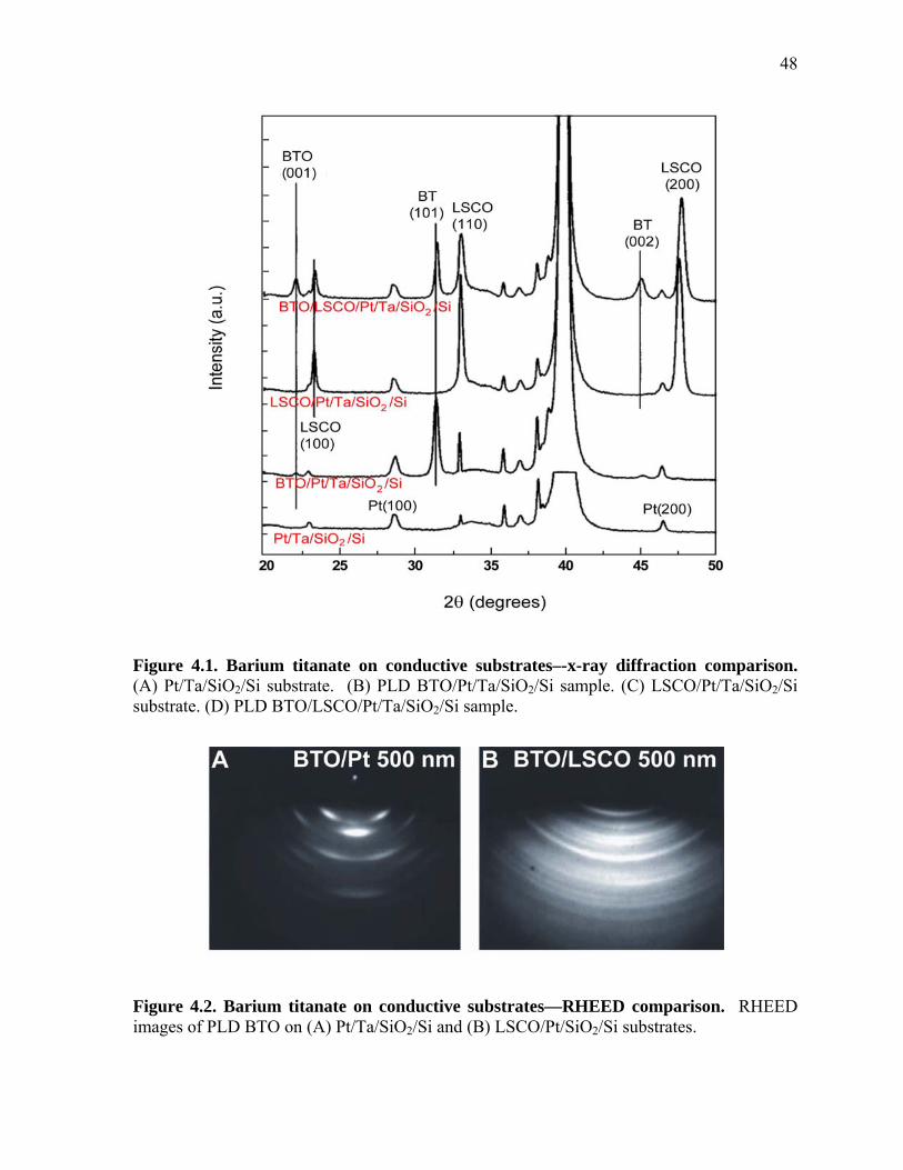
48
Figure 4.1. Barium titanate on conductive substrates–-x-ray diffraction comparison. (A) Pt/Ta/SiO2/Si substrate. (B) PLD BTO/Pt/Ta/SiO2/Si sample. (C) LSCO/Pt/Ta/SiO2/Si substrate. (D) PLD BTO/LSCO/Pt/Ta/SiO2/Si sample.
Figure 4.2. Barium titanate on conductive substrates—RHEED comparison. RHEED images of PLD BTO on (A) Pt/Ta/SiO2/Si and (B) LSCO/Pt/SiO2/Si substrates.
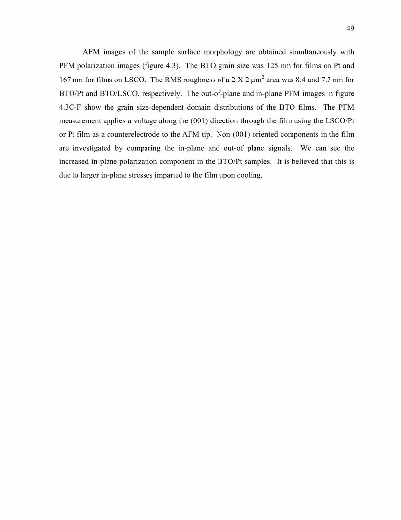
49
AFM images of the sample surface morphology are obtained simultaneously with
PFM polarization images (figure 4.3). The BTO grain size was 125 nm for films on Pt and
167 nm for films on LSCO. The RMS roughness of a 2 X 2 m2 area was 8.4 and 7.7 nm for
BTO/Pt and BTO/LSCO, respectively. The out-of-plane and in-plane PFM images in figure
4.3C-F show the grain size-dependent domain distributions of the BTO films. The PFM
measurement applies a voltage along the (001) direction through the film using the LSCO/Pt
or Pt film as a counterelectrode to the AFM tip. Non-(001) oriented components in the film
are investigated by comparing the in-plane and out-of plane signals. We can see the
increased in-plane polarization component in the BTO/Pt samples. It is believed that this is
due to larger in-plane stresses imparted to the film upon cooling.
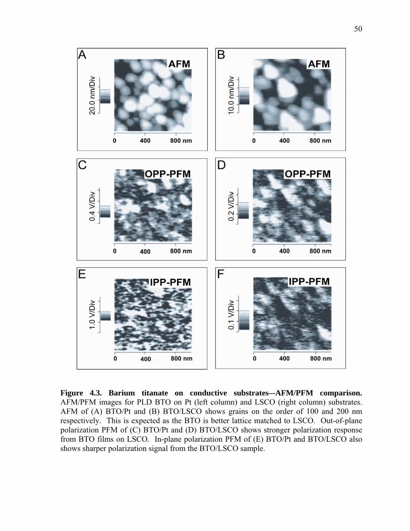
50
Figure 4.3. Barium titanate on conductive substrates–-AFM/PFM comparison. AFM/PFM images for PLD BTO on Pt (left column) and LSCO (right column) substrates. AFM of (A) BTO/Pt and (B) BTO/LSCO shows grains on the order of 100 and 200 nm respectively. This is expected as the BTO is better lattice matched to LSCO. Out-of-plane polarization PFM of (C) BTO/Pt and (D) BTO/LSCO shows stronger polarization response from BTO films on LSCO. In-plane polarization PFM of (E) BTO/Pt and BTO/LSCO also shows sharper polarization signal from the BTO/LSCO sample.
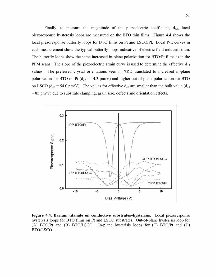
51
Finally, to measure the magnitude of the piezoelectric coefficient, d33, local
piezoresponse hysteresis loops are measured on the BTO thin films. Figure 4.4 shows the
local piezoresponse butterfly loops for BTO films on Pt and LSCO/Pt. Local P-E curves in
each measurement show the typical butterfly loops indicative of electric field induced strain.
The butterfly loops show the same increased in-plane polarization for BTO/Pt films as in the
PFM scans. The slope of the piezoelectric strain curve is used to determine the effective d33
values. The preferred crystal orientations seen in XRD translated to increased in-plane
polarization for BTO on Pt (d33 = 14.3 pm/V) and higher out-of plane polarization for BTO
on LSCO (d33 = 54.0 pm/V). The values for effective d33 are smaller than the bulk value (d33
= 85 pm/V) due to substrate clamping, grain size, defects and orientation effects.
Figure 4.4. Barium titanate on conductive substrates–hysterisis. Local piezoresponse hysteresis loops for BTO films on Pt and LSCO substrates. Out-of-plane hysterisis loop for (A) BTO/Pt and (B) BTO/LSCO. In-plane hysterisis loops for (C) BTO/Pt and (D) BTO/LSCO.
52
4.1.2 Conclusion
The effects of crystal orientation on the piezoelectric properties of BTO thin films
grown on Pt and LSCO/Pt electrodes have been investigated. Thin films deposited on Pt
exhibit strong (101) orientation whereas films deposited on LSCO electrodes show mixed
(001) and (101) orientations. The increase of the in-plane polarization signal in BTO thin
films on Pt is related to the preferred (101) orientation of the polycrystalline films. The
ferroelectric domains are thought to be clamped and stressed by the planar and biaxial
stresses exerted by the substrate and lattice mismatch.
4.2 Mechanical Domain Switching
Nanoindentation, performed in conjunction with PFM, was used to study domain
switching and to measure the mechanical properties of individual ferroelectric domains in
tetragonal BTO. Nanoindentation induces local domain switching and allows the mechanical
differences between a- and c-domains to be investigated. The elastic moduli of a- and c-
domains were mapped to confirm their differences.
4.2.1 Nanoindentation
It is well known that the application of mechanical stress or electrical field can
change the domain structure in ferroelectrics (Fang et al. 2002, Holt et al. 2005, Li et al.
2005, Li et al. 1992, Park et al. 2004, Rogan et al. 2003). As device size shrinks,
ferroelectric components consist of only a few domains and the properties of individual
domains play a critical role in design, fabrication and function of the entire device. The
mechanical properties of individual a- and c-domains, such as Young’s modulus, are not well
characterized on the nanoscale. Characterization of ferroelectric domains at these small
dimensions is challenging for existing mechanical testing techniques. AFM operated in
piezoresponse mode, PFM, has been developed to image surface morphology as well as
polarization domains. Recently, scanning nanoindentation has emerged as a technique for
modulus mapping a surface (Bhushan et al. 2003, Li et al. 2002, Li et al. 2003, Oliver et al.
1992). Using PFM and scanning nanoindentation, the mechanical properties of individual a-
and c-domains are reported for the first time.
This work focuses on (001) oriented, single crystal BTO. Individual domains are
investigated using polarized optical microscopy and contact mode AFM. During AFM
53
surface imaging, domain information is collected in situ via piezoresponse signal with a lock-
in amplifier. PFM imaging is preformed through n-doped silicon cantilevers, modulated with
an AC voltage from 3 to 5 V at 1-2 kHz with a scan rate of 0.3 Hz. A nanoindenter
monitored and recorded the load and displacement of a three-sided diamond pyramid
indenter with a force resolution of 1 nN and a displacement resolution of 0.1 nm. A series of
nanoindentations were made on individual a- and c-domains in BTO. A typical indentation
experiment consisted of three steps: approaching the surface, loading to peak load (5 mN),
and unloading. Elastic modulus and hardness were calculated from the load-displacement
curves.
The surface morphology and domain structure of ferroelectric BTO is reported here.
Figure 4.5A shows a schematic for the strip domain structure found in bulk tetragonal BTO.
The lines represent typical piezoresponse signal intensity along alternating a- and c-domains
during a PFM measurement and corresponding AFM scan (Kalinin et al. 2002b). The
schematic represents domains with a downward polarization as “c+” domains because they
will yield a positive deflection in the tip which is positively biased. In-plane domains show
no signal during the out-of-plane PFM measurement. Figure 4.5B shows the polarized
optical microscopy image of the BTO. The domain size is in the range of 2–10 microns. The
c- and a-domains appear dark and light in the polarized image, respectively, due to the
birefringence difference. Figure 4.5C shows the XRD and RHEED patterns indicative of
BTO. The XRD shows (100)/(001) peak splitting due to the tetragonal structure.
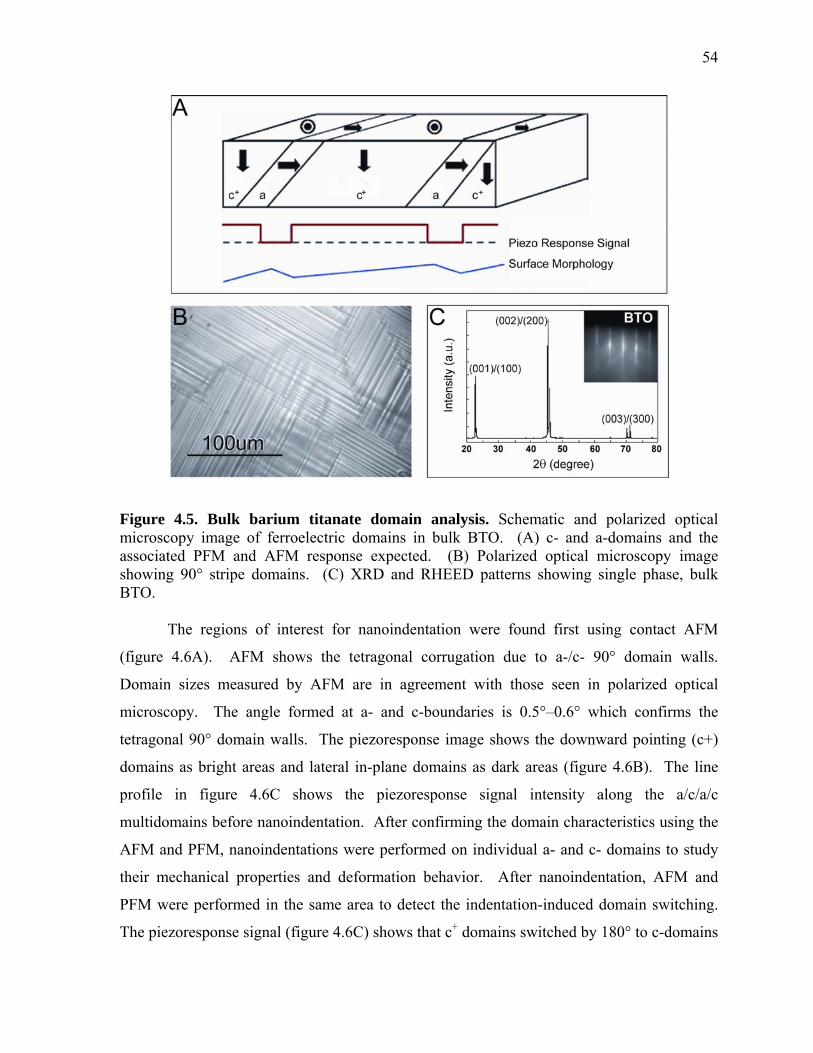
54
Figure 4.5. Bulk barium titanate domain analysis. Schematic and polarized optical microscopy image of ferroelectric domains in bulk BTO. (A) c- and a-domains and the associated PFM and AFM response expected. (B) Polarized optical microscopy image showing 90° stripe domains. (C) XRD and RHEED patterns showing single phase, bulk BTO. The regions of interest for nanoindentation were found first using contact AFM
(figure 4.6A). AFM shows the tetragonal corrugation due to a-/c- 90° domain walls.
Domain sizes measured by AFM are in agreement with those seen in polarized optical
microscopy. The angle formed at a- and c-boundaries is 0.5°–0.6° which confirms the
tetragonal 90° domain walls. The piezoresponse image shows the downward pointing (c+)
domains as bright areas and lateral in-plane domains as dark areas (figure 4.6B). The line
profile in figure 4.6C shows the piezoresponse signal intensity along the a/c/a/c
multidomains before nanoindentation. After confirming the domain characteristics using the
AFM and PFM, nanoindentations were performed on individual a- and c- domains to study
their mechanical properties and deformation behavior. After nanoindentation, AFM and
PFM were performed in the same area to detect the indentation-induced domain switching.
The piezoresponse signal (figure 4.6C) shows that c+ domains switched by 180° to c-domains
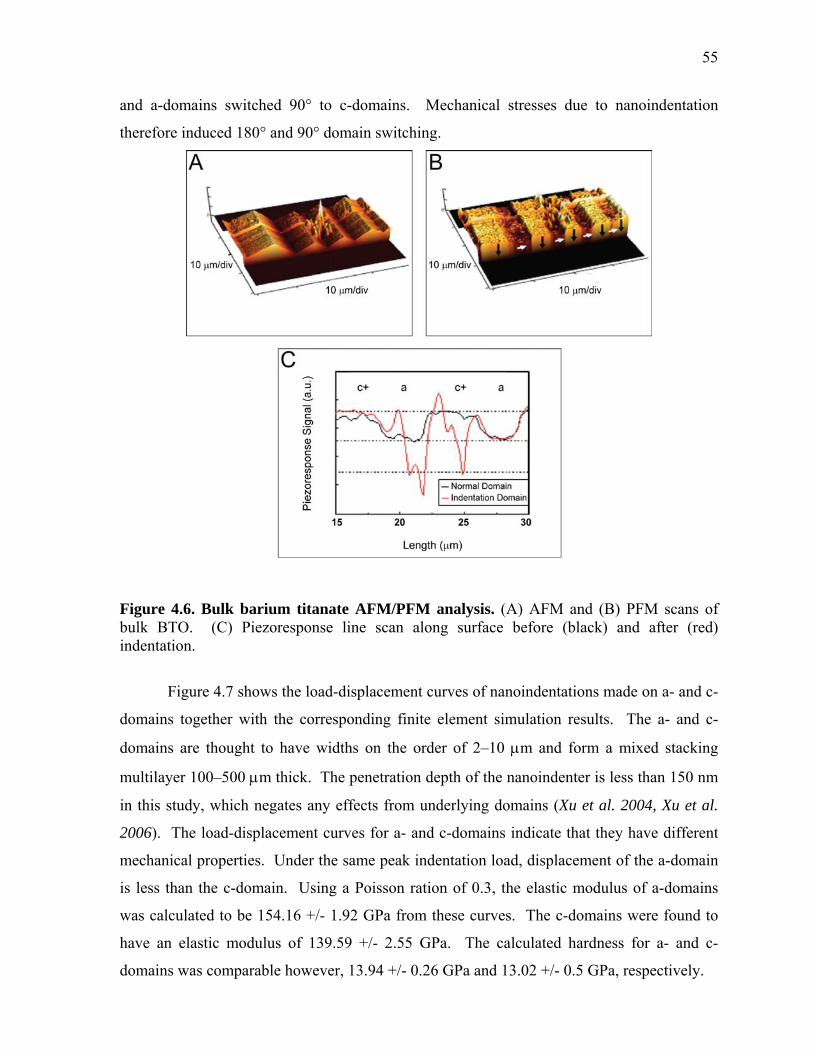
55
and a-domains switched 90° to c-domains. Mechanical stresses due to nanoindentation
therefore induced 180° and 90° domain switching.
Figure 4.6. Bulk barium titanate AFM/PFM analysis. (A) AFM and (B) PFM scans of bulk BTO. (C) Piezoresponse line scan along surface before (black) and after (red) indentation.
Figure 4.7 shows the load-displacement curves of nanoindentations made on a- and c-
domains together with the corresponding finite element simulation results. The a- and c-
domains are thought to have widths on the order of 2–10 m and form a mixed stacking
multilayer 100–500 m thick. The penetration depth of the nanoindenter is less than 150 nm
in this study, which negates any effects from underlying domains (Xu et al. 2004, Xu et al.
2006). The load-displacement curves for a- and c-domains indicate that they have different
mechanical properties. Under the same peak indentation load, displacement of the a-domain
is less than the c-domain. Using a Poisson ration of 0.3, the elastic modulus of a-domains
was calculated to be 154.16 +/- 1.92 GPa from these curves. The c-domains were found to
have an elastic modulus of 139.59 +/- 2.55 GPa. The calculated hardness for a- and c-
domains was comparable however, 13.94 +/- 0.26 GPa and 13.02 +/- 0.5 GPa, respectively.
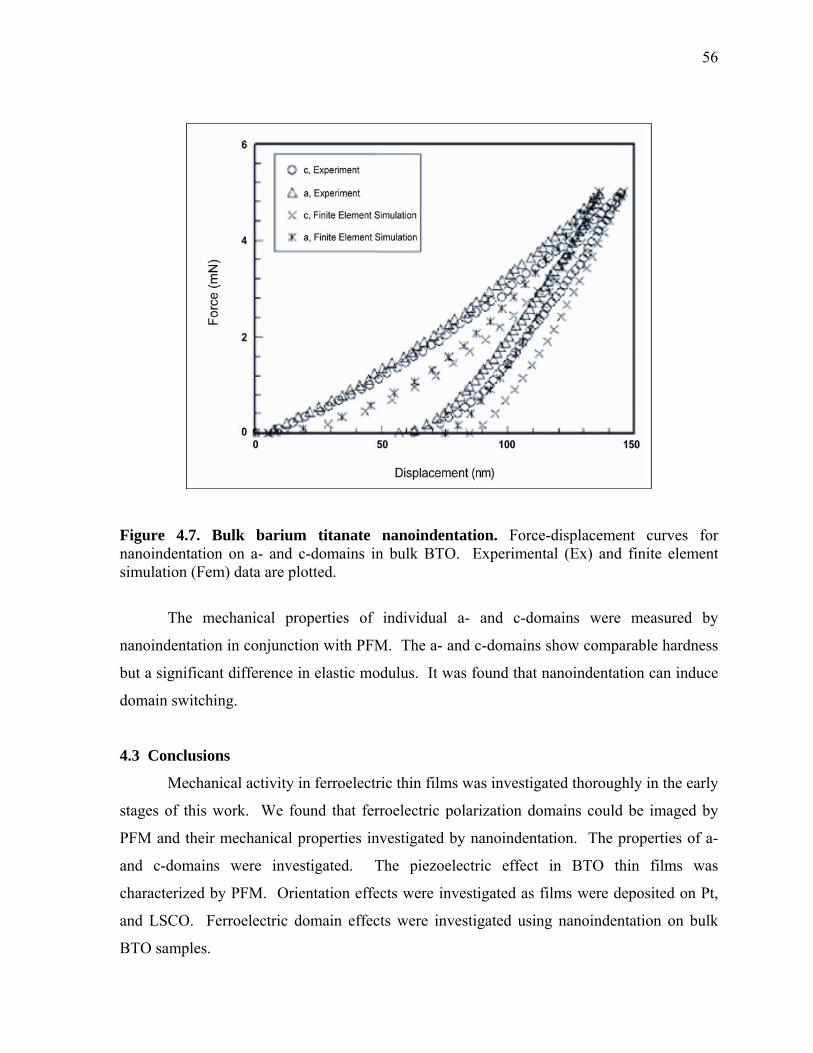
56
Figure 4.7. Bulk barium titanate nanoindentation. Force-displacement curves for nanoindentation on a- and c-domains in bulk BTO. Experimental (Ex) and finite element simulation (Fem) data are plotted.
The mechanical properties of individual a- and c-domains were measured by
nanoindentation in conjunction with PFM. The a- and c-domains show comparable hardness
but a significant difference in elastic modulus. It was found that nanoindentation can induce
domain switching.
4.3 Conclusions
Mechanical activity in ferroelectric thin films was investigated thoroughly in the early
stages of this work. We found that ferroelectric polarization domains could be imaged by
PFM and their mechanical properties investigated by nanoindentation. The properties of a-
and c-domains were investigated. The piezoelectric effect in BTO thin films was
characterized by PFM. Orientation effects were investigated as films were deposited on Pt,
and LSCO. Ferroelectric domain effects were investigated using nanoindentation on bulk
BTO samples.
57
Chapter 5
Active Oxide Thin Films – Optical Studies
Engineering the optical properties of active oxide materials begins with deposition
conditions. Complex oxide thin films are very sensitive to oxygen stoichiometry, and
therefore, oxygen conditions during growth. In this chapter, we draw on work done to show
the effect of oxygen conditions on the complex index of refraction of BTO thin films†. We
present VASE as a characterization technique for the optical properties of active oxide thin
films. A VASE model is developed to determine the index of refraction and absorption of
thin films of BTO grown by MBE and PLD. Finally, two models are presented for VO2
which describes the optical properties of the material in the semiconducting phase and the
metallic phase.
5.1 Background
Integration of electrooptic materials with Si substrates allows for compact optical
components capable of high frequency modulation, such as electrooptic modulators, to be
developed using conventional CMOS processes. The ferroelectric perovskite BTO is an
interesting candidate for thin film optical devices because of its large electrooptic coefficients
and electrically switchable structural and optical properties. While growth of various oxide
thin films has been demonstrated on Si, these films cannot support waveguiding modes due
to low index contrast and the presence of cracks in thick films (Lisoni et al. 2001, McKee et
al. 1991). Optical quality perovskite oxide thin films grown on sufficiently thick, low optical
index template layers would allow for electrooptic thin film waveguides, modulators and
statically tunable photonic devices to be designed and fabricated on Si and Si-compatible
substrates. Previous attempts to grow thin BTO films on template layers has led to
polycrystalline films on Si substrates (Lisoni et al. 2001) while oriented BTO films have
been achieved via growth on MgO films deposited on Al2O3 (Lipinsky et al. 2005).
Ferroelectric thin films can be grown using PLD (Beckers et al. 1998), metal organic
chemical vapor deposition (Beckers et al. 1998, El-Naggar et al. 2005, Kwak et al. 1991),
† Material used in this chapter is compiled from work done in Dicken et al. 2007.
58
sol-gel synthesis (Wills et al. 1992) and MBE (Lemoine et al. 1994, McKee et al. 1991).
MBE can be used to grow complex oxide thin film structures with atomic layer accuracy
(Schlom et al. 2001). High quality ferroelectric thin films are generally grown on lattice
matched substrates such as MgO and STO. Integration of ferroelectric thin films with Si
processing may enable the properties of ferroelectrics to be utilized in combination with
CMOS in multi-material integration. IBAD of various template layers such as MgO and
yttria-stabilized zirconia has been used to develop thin films of superconducting YBa2Cu3O7
as well as oriented layers of (Pb,Ba)TiO3 (Brewer & Atwater 2002, Wang et al. 1997).
We have developed processes for growth by IBAD of biaxially oriented MgO films
that act as templates for growth of highly textured ferroelectric perovskite oxide films
(Brewer & Atwater 2002). So far, however, well oriented, optical-quality BTO films
integrated with amorphous substrates in conjunction with Si-based substrates have not been
realized. In this chapter we investigate growth of highly textured BTO films on various
substrates using different oxidation sources and establish models to fit the optical properties
of BTO thin films in order to compare with single crystal BTO.
5.2 Optical Properties of Textured Barium Titanate Thin Films
We have investigated the growth of BTO thin films on bulk crystalline and
amorphous substrates utilizing biaxially oriented template layers. IBAD was used to grow
thin, biaxially textured, MgO template layers on amorphous and Si substrates. Growth of
highly oriented BTO films on these template layers was achieved by MBE using a layer-by-
layer growth process. BTO thin films were grown in molecular oxygen and in the presence
of oxygen radicals produced by a RF plasma. We used x-ray and in situ RHEED to analyze
the structural properties and show the predominately c-oriented grains in the films. VASE
was used to analyze and compare the optical properties of the thin films grown with and
without oxygen plasma. We have shown that optical quality BTO thin films, which show
bulk crystal-like properties, can be grown on any substrate through the use of biaxially
oriented MgO template layers.
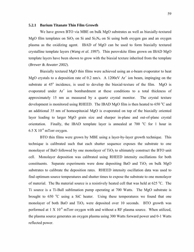
59
5.2.1 Barium Titanate Thin Film Growth
We have grown BTO via MBE on bulk MgO substrates as well as biaxially-textured
MgO film templates on SiO2 on Si and Si3N4 on Si using both oxygen gas and an oxygen
plasma as the oxidizing agent. IBAD of MgO can be used to form biaxially textured
crystalline template layers (Wang et al. 1997). Thin perovskite films grown on IBAD MgO
template layers have been shown to grow with the biaxial texture inherited from the template
(Brewer & Atwater 2002).
Biaxially textured MgO thin films were achieved using an e-beam evaporator to heat
MgO crystals to a deposition rate of 0.2 nm/s. A 1200eV Ar+ ion beam, impinging on the
substrate at 45o incidence, is used to develop the biaxial-texture of the film. MgO is
evaporated under Ar+ ion bombardment at these conditions to a total thickness of
approximately 15 nm as measured by a quartz crystal monitor. The crystal texture
development is monitored using RHEED. The IBAD MgO film is then heated to 650 oC and
an additional 35 nm of homoepitaxial MgO is evaporated on top of the biaxially oriented
layer leading to larger MgO grain size and sharper in-plane and out-of-plane crystal
orientation. Finally, the IBAD template layer is annealed at 700 oC for 1 hour in
6.5 X 10⁻⁶ mTorr oxygen.
BTO thin films were grown by MBE using a layer-by-layer growth technique. This
technique is calibrated such that each shutter sequence exposes the substrate to one
monolayer of BaO followed by one monolayer of TiO2 to ultimately construct the BTO unit
cell. Monolayer deposition was calibrated using RHEED intensity oscillations for both
constituents. Separate experiments were done depositing BaO and TiO2 on bulk MgO
substrates to calibrate the deposition rates. RHEED intensity oscillation data was used to
find optimum source temperatures and shutter times to expose the substrate to one monolayer
of material. The Ba material source is a resistively heated cell that was held at 625 oC. The
Ti source is a Ti-Ball sublimation pump operating at 700 Watts. The MgO substrate is
brought to 650 oC using a SiC heater. Using these temperatures we found that one
monolayer of both BaO and TiO2 were deposited over 10 seconds. BTO growth was
performed at 1 X 10⁻⁶ mTorr oxygen with and without a RF plasma source. When utilized,
the plasma source generates an oxygen plasma using 300 Watts forward power and 0-1 Watts
reflected power.
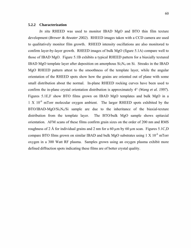
60
5.2.2 Characterization
In situ RHEED was used to monitor IBAD MgO and BTO thin film texture
development (Brewer & Atwater 2002). RHEED images taken with a CCD camera are used
to qualitatively monitor film growth. RHEED intensity oscillations are also monitored to
confirm layer-by-layer growth. RHEED images of bulk MgO (figure 5.1A) compare well to
those of IBAD MgO. Figure 5.1B exhibits a typical RHEED pattern for a biaxially textured
IBAD MgO template layer after deposition on amorphous Si3N4 on Si. Streaks in the IBAD
MgO RHEED pattern attest to the smoothness of the template layer, while the angular
orientation of the RHEED spots show how the grains are oriented out of plane with some
small distribution about the normal. In-plane RHEED rocking curves have been used to
confirm the in-plane crystal orientation distribution is approximately 4° (Wang et al. 1997).
Figures 5.1E,F show BTO films grown on IBAD MgO templates and bulk MgO in a
1 X 10⁻⁶ mTorr molecular oxygen ambient. The larger RHEED spots exhibited by the
BTO/IBAD-MgO/Si3N4/Si sample are due to the inheritance of the biaxial-texture
distribution from the template layer. The BTO/bulk MgO sample shows epitaxial
orientation. AFM scans of these films confirm grain sizes on the order of 200 nm and RMS
roughness of 2 Å for individual grains and 2 nm for a 60 m by 60 m scan. Figures 5.1C,D
compare BTO films grown on similar IBAD and bulk MgO substrates using 1 X 10⁻⁶ mTorr
oxygen in a 300 Watt RF plasma. Samples grown using an oxygen plasma exhibit more
defined diffraction spots indicating these films are of better crystal quality.
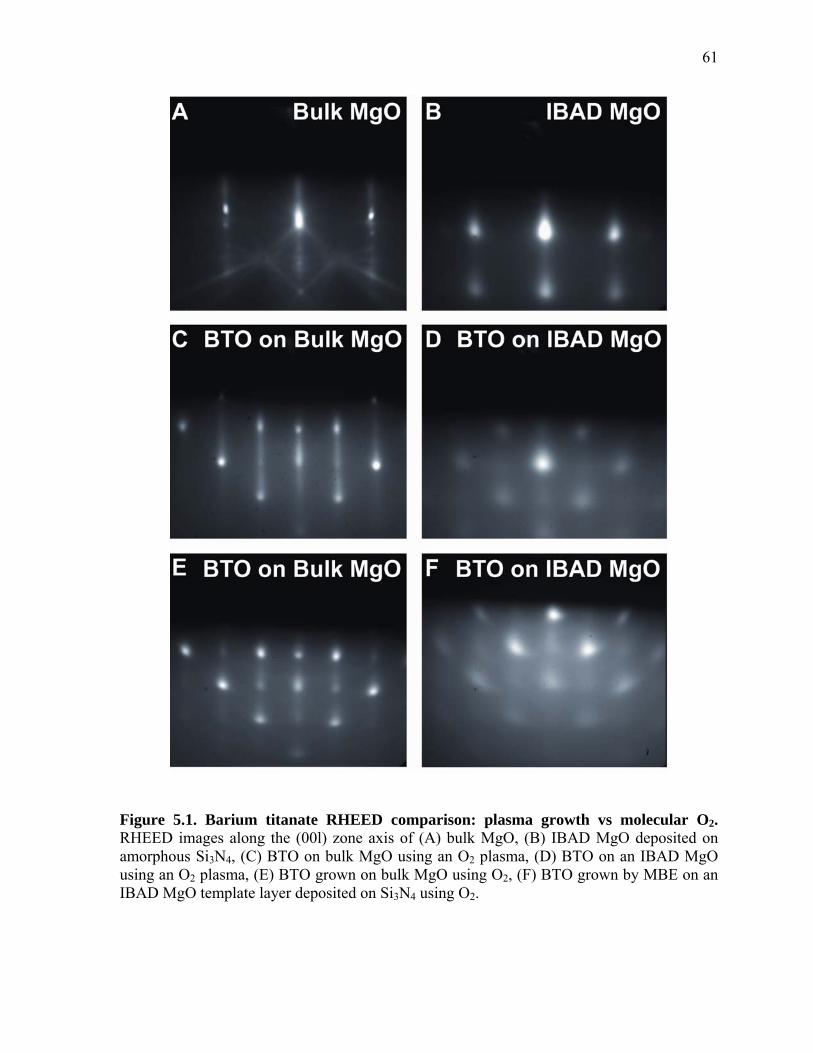
61
Figure 5.1. Barium titanate RHEED comparison: plasma growth vs molecular O2. RHEED images along the (00l) zone axis of (A) bulk MgO, (B) IBAD MgO deposited on amorphous Si3N4, (C) BTO on bulk MgO using an O2 plasma, (D) BTO on an IBAD MgO using an O2 plasma, (E) BTO grown on bulk MgO using O2, (F) BTO grown by MBE on an IBAD MgO template layer deposited on Si3N4 using O2.
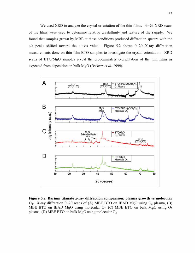
62
We used XRD to analyze the crystal orientation of the thin films. XRD scans
of the films were used to determine relative crystallinity and texture of the sample. We
found that samples grown by MBE at these conditions produced diffraction spectra with the
c/a peaks shifted toward the c-axis value. Figure 5.2 shows X-ray diffraction
measurements done on thin film BTO samples to investigate the crystal orientation. XRD
scans of BTO/MgO samples reveal the predominately c-orientation of the thin films as
expected from deposition on bulk MgO (Beckers et al. 1998).
Figure 5.2. Barium titanate x-ray diffraction comparison: plasma growth vs molecular O2. X-ray diffraction scans of (A) MBE BTO on IBAD MgO using O2 plasma, (B) MBE BTO on IBAD MgO using molecular O2. (C) MBE BTO on bulk MgO using O2 plasma, (D) MBE BTO on bulk MgO using molecular O2.
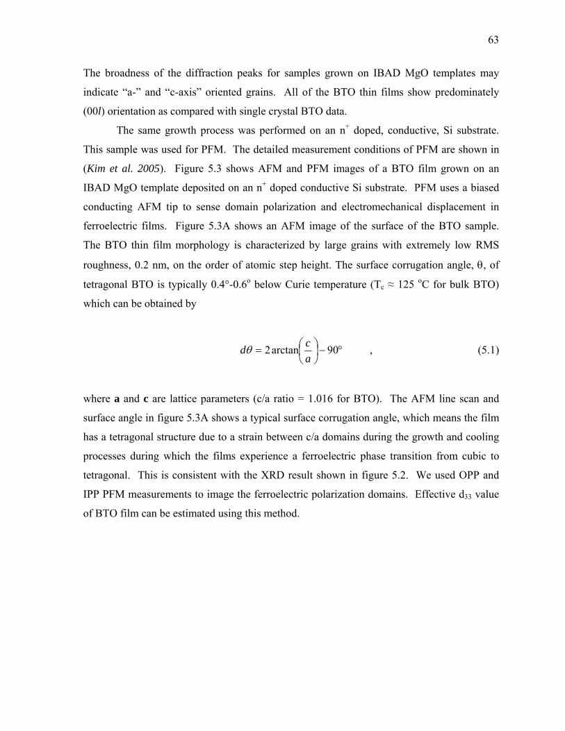
63
The broadness of the diffraction peaks for samples grown on IBAD MgO templates may
indicate “a-” and “c-axis” oriented grains. All of the BTO thin films show predominately
(00l) orientation as compared with single crystal BTO data.
The same growth process was performed on an n+ doped, conductive, Si substrate.
This sample was used for PFM. The detailed measurement conditions of PFM are shown in
(Kim et al. 2005). Figure 5.3 shows AFM and PFM images of a BTO film grown on an
IBAD MgO template deposited on an n+ doped conductive Si substrate. PFM uses a biased
conducting AFM tip to sense domain polarization and electromechanical displacement in
ferroelectric films. Figure 5.3A shows an AFM image of the surface of the BTO sample.
The BTO thin film morphology is characterized by large grains with extremely low RMS
roughness, 0.2 nm, on the order of atomic step height. The surface corrugation angle, , of
tetragonal BTO is typically 0.4°-0.6o below Curie temperature (Tc ≈ 125 oC for bulk BTO)
which can be obtained by
90arctan2
a
cd , (5.1)
where a and c are lattice parameters (c/a ratio = 1.016 for BTO). The AFM line scan and
surface angle in figure 5.3A shows a typical surface corrugation angle, which means the film
has a tetragonal structure due to a strain between c/a domains during the growth and cooling
processes during which the films experience a ferroelectric phase transition from cubic to
tetragonal. This is consistent with the XRD result shown in figure 5.2. We used OPP and
IPP PFM measurements to image the ferroelectric polarization domains. Effective d33 value
of BTO film can be estimated using this method.
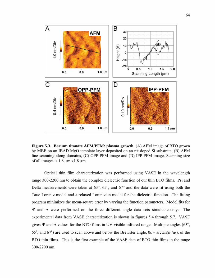
64
Figure 5.3. Barium titanate AFM/PFM: plasma growth. (A) AFM image of BTO grown by MBE on an IBAD MgO template layer deposited on an n+ doped Si substrate, (B) AFM line scanning along domains, (C) OPP-PFM image and (D) IPP-PFM image. Scanning size of all images is 1.8 m x1.8 m
Optical thin film characterization was performed using VASE in the wavelength
range 300-2200 nm to obtain the complex dielectric function of our thin BTO films. Psi and
Delta measurements were taken at 63°, 65°, and 67° and the data were fit using both the
Tauc-Lorentz model and a relaxed Lorentzian model for the dielectric function. The fitting
program minimizes the mean-square error by varying the function parameters. Model fits for
and were performed on the three different angle data sets simultaneously. The
experimental data from VASE characterization is shown in figures 5.4 through 5.7. VASE
gives and values for the BTO films in UV-visible-infrared range. Multiple angles (63o,
65o, and 67o) are used to scan above and below the Brewster angle, b= arctan(n1/n2), of the
BTO thin films. This is the first example of the VASE data of BTO thin films in the range
300-2200 nm.
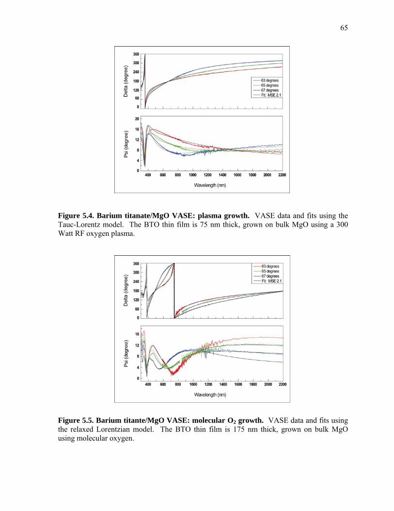
65
Figure 5.4. Barium titanate/MgO VASE: plasma growth. VASE data and fits using the Tauc-Lorentz model. The BTO thin film is 75 nm thick, grown on bulk MgO using a 300 Watt RF oxygen plasma.
Figure 5.5. Barium titante/MgO VASE: molecular O2 growth. VASE data and fits using the relaxed Lorentzian model. The BTO thin film is 175 nm thick, grown on bulk MgO using molecular oxygen.
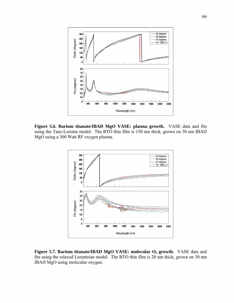
66
Figure 5.6. Barium titanate/IBAD MgO VASE: plasma growth. VASE data and fits using the Tauc-Lorentz model. The BTO thin film is 150 nm thick, grown on 30 nm IBAD MgO using a 300 Watt RF oxygen plasma.
Figure 5.7. Barium titanate/IBAD MgO VASE: molecular O2 growth. VASE data and fits using the relaxed Lorentzian model. The BTO thin film is 20 nm thick, grown on 30 nm IBAD MgO using molecular oxygen.
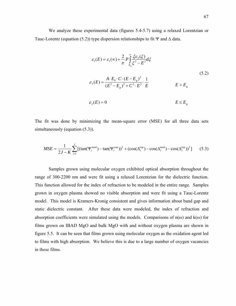
67
We analyze these experimental data (figures 5.4-5.7) using a relaxed Lorentzian or
Tauc-Lorentz (equation (5.2)) type dispersion relationships to fit and data.
dE
PEgE
222
11
)(2)()(
(5.2)
The fit was done by minimizing the mean-square error (MSE) for all three data sets
simultaneously (equation (5.3)).
J
iiiiiiKJ
MSE1
2expmodexp2expmod ]))cos()cos()(cos())tan()[(tan(2
1 (5.3)
Samples grown using molecular oxygen exhibited optical absorption throughout the
range of 300-2200 nm and were fit using a relaxed Lorentzian for the dielectric function.
This function allowed for the index of refraction to be modeled in the entire range. Samples
grown in oxygen plasma showed no visible absorption and were fit using a Tauc-Lorentz
model. This model is Kramers-Kronig consistent and gives information about band gap and
static dielectric constant. After these data were modeled, the index of refraction and
absorption coefficients were simulated using the models. Comparisons of n() and k() for
films grown on IBAD MgO and bulk MgO with and without oxygen plasma are shown in
figure 5.5. It can be seen that films grown using molecular oxygen as the oxidation agent led
to films with high absorption. We believe this is due to a large number of oxygen vacancies
in these films.
EECEE
EECEAE
g
g 1
)(
)()(
2222
20
2
0)(2 E
gEE
gEE
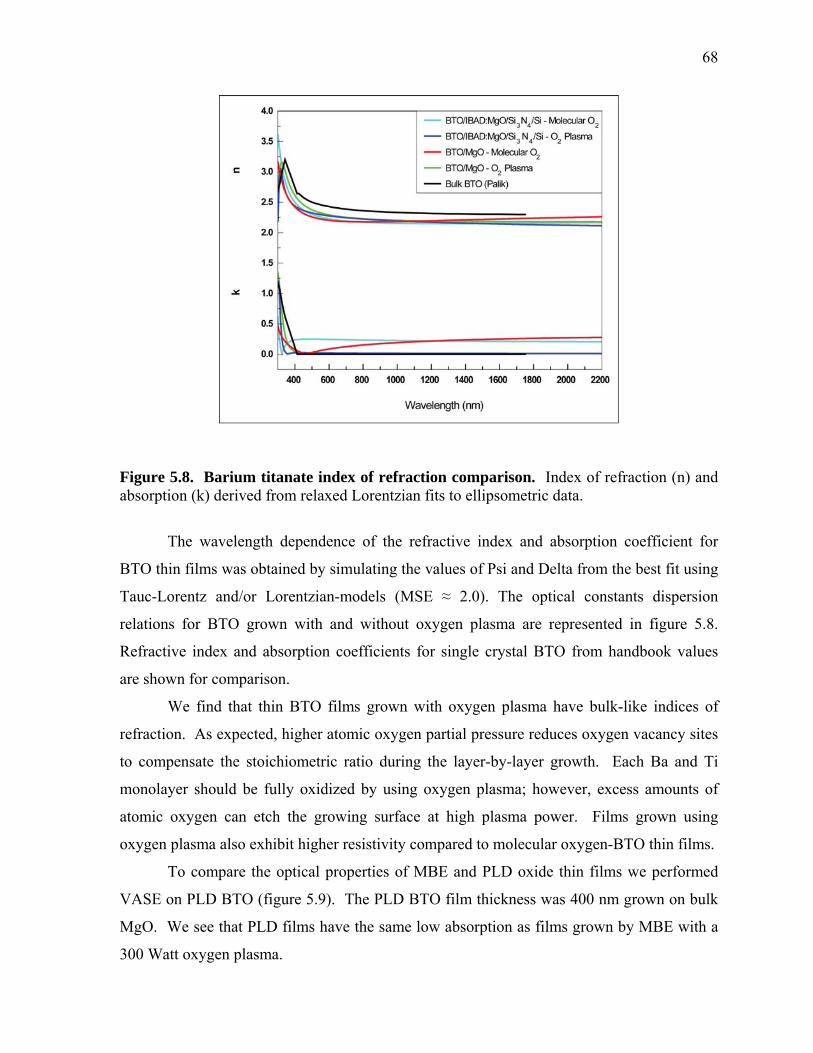
68
Figure 5.8. Barium titanate index of refraction comparison. Index of refraction (n) and absorption (k) derived from relaxed Lorentzian fits to ellipsometric data.
The wavelength dependence of the refractive index and absorption coefficient for
BTO thin films was obtained by simulating the values of Psi and Delta from the best fit using
Tauc-Lorentz and/or Lorentzian-models (MSE ≈ 2.0). The optical constants dispersion
relations for BTO grown with and without oxygen plasma are represented in figure 5.8.
Refractive index and absorption coefficients for single crystal BTO from handbook values
are shown for comparison.
We find that thin BTO films grown with oxygen plasma have bulk-like indices of
refraction. As expected, higher atomic oxygen partial pressure reduces oxygen vacancy sites
to compensate the stoichiometric ratio during the layer-by-layer growth. Each Ba and Ti
monolayer should be fully oxidized by using oxygen plasma; however, excess amounts of
atomic oxygen can etch the growing surface at high plasma power. Films grown using
oxygen plasma also exhibit higher resistivity compared to molecular oxygen-BTO thin films.
To compare the optical properties of MBE and PLD oxide thin films we performed
VASE on PLD BTO (figure 5.9). The PLD BTO film thickness was 400 nm grown on bulk
MgO. We see that PLD films have the same low absorption as films grown by MBE with a
300 Watt oxygen plasma.
69
Figure 5.9. VASE of pulsed laser deposition barium titanate. The optical quality of PLD BTO is comparable to MBE films grown in an oxygen plasma. Data were fit using a Tauc-Lorentz function similar to MBE films (equation (5.1)).
70
5.2.3 Conclusion
In summary, highly textured and optically active BTO thin films were grown by
layer-by-layer MBE on various crystal substrates by using IBAD MgO template which
allows the growth of BTO films on amorphous and Si-based substrates. X-ray diffraction
and in situ RHEED analyses show the highly textured c-orientation of the BTO films on both
IBAD MgO/a-Si3N4/Si and bulk MgO substrates independent of oxidation methods. Optical
properties of the BTO films show bulk-like dispersion relations, but films grown using
molecular oxygen exhibit large optical absorption throughout the wavelength range 300—
2200 nm. Utilizing an oxygen plasma ambient during growth helps to develop optically
transparent and stoichiometric BTO film growth on any substrate. In addition, PLD BTO
films are of comparable optical quality to MBE films.
5.3 Optical Properties of Vanadium Oxide Thin Films
Vanadium (II) oxide (VO2) is a transparent semiconductor at room temperature.
Above 70° C, VO2 undergoes a metal-insulator transition (MIT) which is accompanied by a
large change in the material optical properties. We use VASE to measure the optical
properties of both phases of VO2 and develop a separate optical model for each phase to
extract the complex index of refraction. VASE data for VO2 at room temperature, during
heating with a conventional heat gun, and above its MIT temperature are shown in figure
5.10. The complex index of refraction for VO2 was modeled at room temperature and above
the metal transition temperature. At room temperature, VO2 can be modeled as a Tauc-
Lorentz layer, similar to BTO, above its MIT it is modeled as a Drude metal. The and
data were fit using these models and n and k (1 and 2) as a function of wavelength were
extracted (figure 5.11). The complex index of refraction for each VO2 sample can be found
using this procedure. These data are used to model the VO2 layer in the metamaterial
structures discussed in chapter 7.
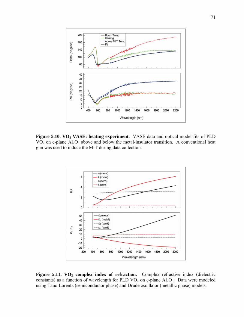
71
Figure 5.10. VO2 VASE: heating experiment. VASE data and optical model fits of PLD VO2 on c-plane Al2O3 above and below the metal-insulator transition. A conventional heat gun was used to induce the MIT during data collection.
Figure 5.11. VO2 complex index of refraction. Complex refractive index (dielectric constants) as a function of wavelength for PLD VO2 on c-plane Al2O3. Data were modeled using Tauc-Lorentz (semiconductor phase) and Drude oscillator (metallic phase) models.

72
Part III
Active Metal-Oxide Nanophotonics
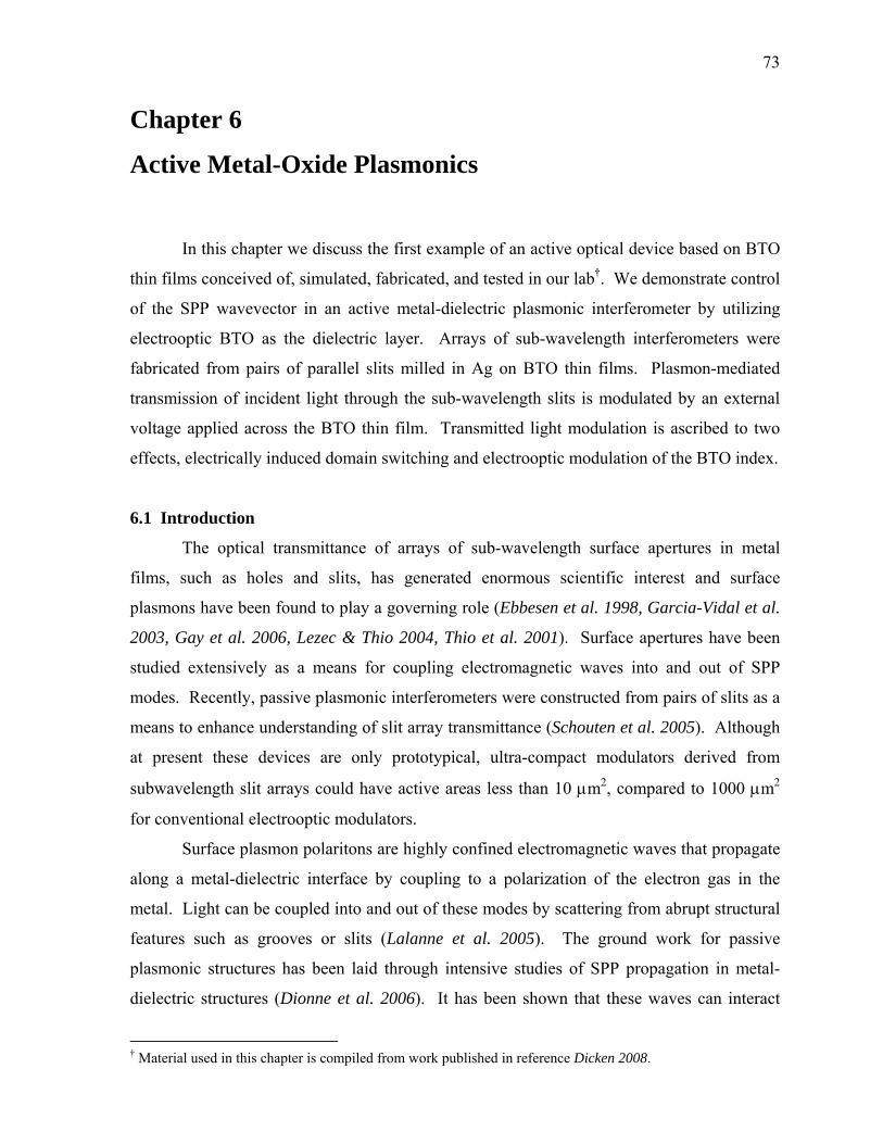
73
Chapter 6
Active Metal-Oxide Plasmonics
In this chapter we discuss the first example of an active optical device based on BTO
thin films conceived of, simulated, fabricated, and tested in our lab†. We demonstrate control
of the SPP wavevector in an active metal-dielectric plasmonic interferometer by utilizing
electrooptic BTO as the dielectric layer. Arrays of sub-wavelength interferometers were
fabricated from pairs of parallel slits milled in Ag on BTO thin films. Plasmon-mediated
transmission of incident light through the sub-wavelength slits is modulated by an external
voltage applied across the BTO thin film. Transmitted light modulation is ascribed to two
effects, electrically induced domain switching and electrooptic modulation of the BTO index.
6.1 Introduction
The optical transmittance of arrays of sub-wavelength surface apertures in metal
films, such as holes and slits, has generated enormous scientific interest and surface
plasmons have been found to play a governing role (Ebbesen et al. 1998, Garcia-Vidal et al.
2003, Gay et al. 2006, Lezec & Thio 2004, Thio et al. 2001). Surface apertures have been
studied extensively as a means for coupling electromagnetic waves into and out of SPP
modes. Recently, passive plasmonic interferometers were constructed from pairs of slits as a
means to enhance understanding of slit array transmittance (Schouten et al. 2005). Although
at present these devices are only prototypical, ultra-compact modulators derived from
subwavelength slit arrays could have active areas less than 10 m2, compared to 1000 m2
for conventional electrooptic modulators.
Surface plasmon polaritons are highly confined electromagnetic waves that propagate
along a metal-dielectric interface by coupling to a polarization of the electron gas in the
metal. Light can be coupled into and out of these modes by scattering from abrupt structural
features such as grooves or slits (Lalanne et al. 2005). The ground work for passive
plasmonic structures has been laid through intensive studies of SPP propagation in metal-
dielectric structures (Dionne et al. 2006). It has been shown that these waves can interact
† Material used in this chapter is compiled from work published in reference Dicken 2008.
74
with light transmitted through slits to create an interference pattern in the overall
transmission intensity and this interference pattern can be affected by changes to the
imaginary part of the SPP wavevector (Pacifici et al. 2007). SPP modulation via the
electrooptic effect has been studied previously in polymer films by coupling light into
surface plasmon modes at a metal-polymer interface (Chyou et al. 2005). Here, we
investigate dynamic modulation of the real part of the SPP wavevector by replacing the
dielectric layer in the structure with an electrooptically active BTO thin solid film.
Barium titanate is a well known perovskite ferroelectric material that exhibits a large
electrooptic coefficient, on the order of r = 100 pm/V, and large birefringence due to its
atomic structure, n = 0.05 (Beckers et al. 1998, Zgonik et al. 1994). Thin films of BTO are
deposited by numerous techniques and their optical properties have been widely investigated
and employed in electrooptic waveguides and modulators (Petraru et al. 2002, Tang et al.
2004a, Tang et al. 2004b). BTO has a tetragonal crystal structure with an ordinary index, no
= 2.412, corresponding to the shorter a-axis, which is larger than the extraordinary index, ne
= 2.36, along the longer c-axis. Ferroelectric domains form when the film is cooled below
the Curie temperature of 120 oC and their final orientation is affected by film stresses, as well
as lattice and thermal expansion mismatch. Ferroelectric domains in BTO can be
characterized by their orientation in-plane (a-axis) or out-of-plane (c-axis). BTO thin films
deposited on oxide thin film electrodes have been characterized by PFM and show both in-
plane and out-of-plane domains (Kim et al. 2005). These domains can be manipulated by
applying an electric field across the material, and in-plane domains can be forced to switch
out-of-plane under an applied field greater than the coercive field. This domain switching
event is accompanied by a large change in the index of the BTO thin film due to the
birefringence in the material. Using BTO thin films, we modulate the real part of the index
of refraction at the Ag/BaTiO3 interface and thereby modulate the SPP wavevector.
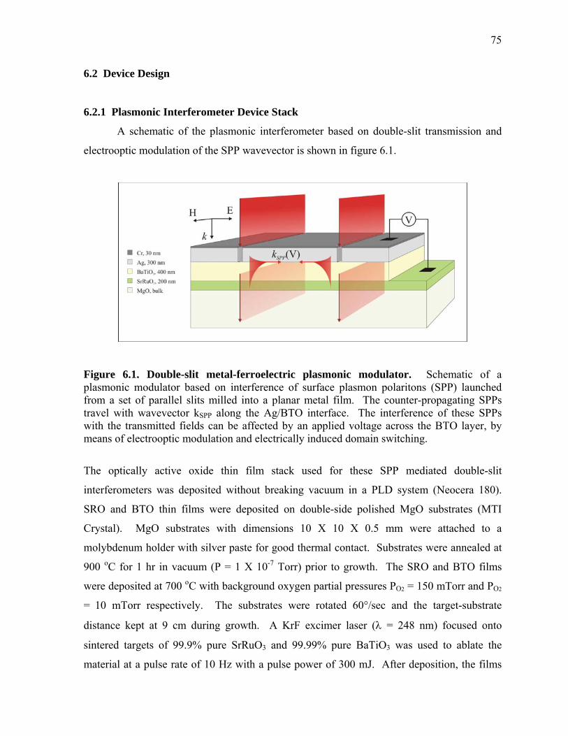
75
6.2 Device Design
6.2.1 Plasmonic Interferometer Device Stack
A schematic of the plasmonic interferometer based on double-slit transmission and
electrooptic modulation of the SPP wavevector is shown in figure 6.1.
Figure 6.1. Double-slit metal-ferroelectric plasmonic modulator. Schematic of a plasmonic modulator based on interference of surface plasmon polaritons (SPP) launched from a set of parallel slits milled into a planar metal film. The counter-propagating SPPs travel with wavevector kSPP along the Ag/BTO interface. The interference of these SPPs with the transmitted fields can be affected by an applied voltage across the BTO layer, by means of electrooptic modulation and electrically induced domain switching.
The optically active oxide thin film stack used for these SPP mediated double-slit
interferometers was deposited without breaking vacuum in a PLD system (Neocera 180).
SRO and BTO thin films were deposited on double-side polished MgO substrates (MTI
Crystal). MgO substrates with dimensions 10 X 10 X 0.5 mm were attached to a
molybdenum holder with silver paste for good thermal contact. Substrates were annealed at
900 oC for 1 hr in vacuum (P = 1 X 10⁻⁷ Torr) prior to growth. The SRO and BTO films
were deposited at 700 oC with background oxygen partial pressures PO2 = 150 mTorr and PO2
= 10 mTorr respectively. The substrates were rotated 60°/sec and the target-substrate
distance kept at 9 cm during growth. A KrF excimer laser ( = 248 nm) focused onto
sintered targets of 99.9% pure SrRuO3 and 99.99% pure BaTiO3 was used to ablate the
material at a pulse rate of 10 Hz with a pulse power of 300 mJ. After deposition, the films
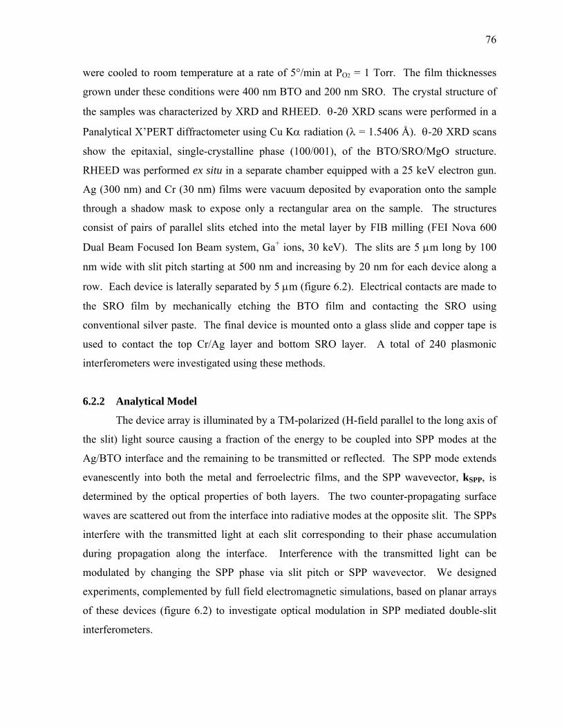
76
were cooled to room temperature at a rate of 5°/min at PO2 = 1 Torr. The film thicknesses
grown under these conditions were 400 nm BTO and 200 nm SRO. The crystal structure of
the samples was characterized by XRD and RHEED. -2 XRD scans were performed in a
Panalytical X’PERT diffractometer using Cu K radiation ( = 1.5406 Å). -2 XRD scans
show the epitaxial, single-crystalline phase (100/001), of the BTO/SRO/MgO structure.
RHEED was performed ex situ in a separate chamber equipped with a 25 keV electron gun.
Ag (300 nm) and Cr (30 nm) films were vacuum deposited by evaporation onto the sample
through a shadow mask to expose only a rectangular area on the sample. The structures
consist of pairs of parallel slits etched into the metal layer by FIB milling (FEI Nova 600
Dual Beam Focused Ion Beam system, Ga+ ions, 30 keV). The slits are 5 m long by 100
nm wide with slit pitch starting at 500 nm and increasing by 20 nm for each device along a
row. Each device is laterally separated by 5 m (figure 6.2). Electrical contacts are made to
the SRO film by mechanically etching the BTO film and contacting the SRO using
conventional silver paste. The final device is mounted onto a glass slide and copper tape is
used to contact the top Cr/Ag layer and bottom SRO layer. A total of 240 plasmonic
interferometers were investigated using these methods.
6.2.2 Analytical Model
The device array is illuminated by a TM-polarized (H-field parallel to the long axis of
the slit) light source causing a fraction of the energy to be coupled into SPP modes at the
Ag/BTO interface and the remaining to be transmitted or reflected. The SPP mode extends
evanescently into both the metal and ferroelectric films, and the SPP wavevector, kSPP, is
determined by the optical properties of both layers. The two counter-propagating surface
waves are scattered out from the interface into radiative modes at the opposite slit. The SPPs
interfere with the transmitted light at each slit corresponding to their phase accumulation
during propagation along the interface. Interference with the transmitted light can be
modulated by changing the SPP phase via slit pitch or SPP wavevector. We designed
experiments, complemented by full field electromagnetic simulations, based on planar arrays
of these devices (figure 6.2) to investigate optical modulation in SPP mediated double-slit
interferometers.
77
Figure 6.2. Double-slit SPP interferometer array. CCD image, collected with a 10X objective, of an array of double-slit devices patterned in Cr/Ag on BTO illuminated by TM-polarized (H-field parallel to the long axis of the slit) 688 nm laser diode light. The slit pitch starts at 0.50 m and increases by 20 nm for each device along a row. The observed intensity oscillation as a function of slit pitch is due to SPP interference with light transmitted through each slit. Insets: Scanning electron micrograph of slit pairs milled by focused ion beam in a Cr on Ag layer. 50X image of devices with slit pitches varying from 1.50 to 1.98 m showing one full period of transmitted intensity oscillation.
A simple analytical treatment of the total transmitted intensity resulting from
interference between the incident field and the SPP field can be used to show that small
changes in the index of refraction of the dielectric layer can lead to significant changes in the
transmitted intensity profile. For this work, the double-slit device is governed by plasmon
interference at the bottom interface of the Ag, due to the highly absorbing Cr layer at the top
surface. Considering the transmission at each slit to be the sum of a transmitted field and a
SPP field that has acquired some phase, oSPP xk , the resulting normalized transmitted
intensity can be expressed as (Pacifici et al. 2008)
78
oSPP
x
ox
ooo
T xkeeI
I
cos21 2'2' , (6.1)
where o and o’ are scattering efficiencies for SPP coupling at each slit, is the absorption
coefficient, kSPP is the SPP wavevector and o is the phase imparted by scattering from the
slit. Data from experiments and full field electromagnetic simulations have been fit by this
model to extract the relative index change of the active BTO layer from
nSPP= EffAgEffAg / where Eff is an effective dielectric constant describing the
properties of all non-metallic layers (Raether 1988).
6.2.3 Finite Difference Time Domain Simulations
To explore the physics of this double-slit device, simulations were performed using
full field finite-difference time-domain software (FDTD) (OptiFDTD 2005). A multi-
oscillator Lorentz-Drude model is used for the Cr and Ag layers with parameters given by
Rakic et al. (Rakic et al. 1998). The BTO and SRO complex refractive index data used were
derived from VASE measurements (Dicken et al. 2007). Figure 6.3A shows the magnetic
field profile (Hy) for one device with a slit pitch of 1.50 m and an index of refraction, nBTO,
of 2.20 for the BTO layer. The input plane wave ( = 688 nm) from Z = 1 m is transmitted
through the 100 nm wide slits and a fraction is scattered into surface plasmon polariton
modes propagating along the Ag/BTO interface to the left and right of each slit. Counter-
propagating SPPs along the interferometer arm formed between the slits interfere
constructively or destructively depending on slit pitch and SPP wavevector. Figure 6.3B
shows the absolute magnetic field (|Hy|2) from the same simulation. The resonant mode
formed by the two counter-propagating SPPs inside the cavity can be identified in this figure.
SPPs propagating away from each slit appear in the form of a continuously decaying
intensity profile along the Ag/BTO interface. Figure 6.3B also shows fields being coupled
into a waveguide mode formed by the 400 nm BTO film. At each slit, a fraction of the
incoming energy scatters out of the SPP mode and interferes with the transmitted light to
create an overall modulation in the transmitted power. The optical power flow through the
device can be analyzed for these simulations by plotting the Poynting vector (Sz) (figure
6.3C).
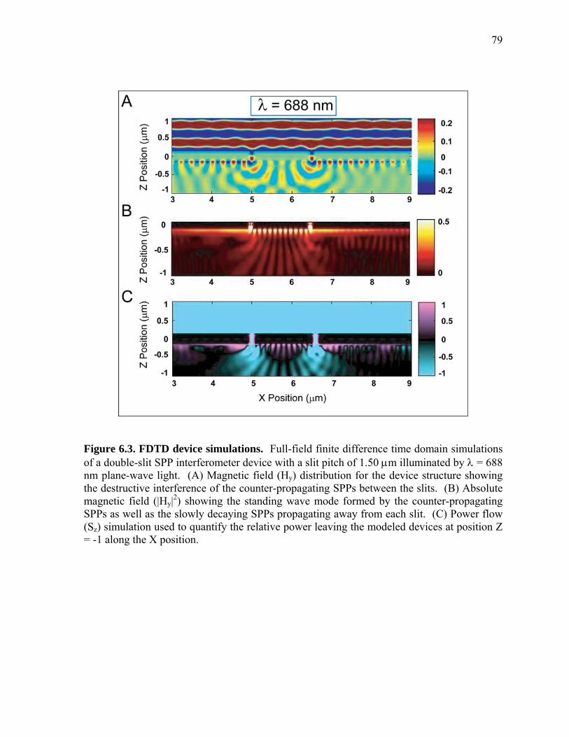
79
Figure 6.3. FDTD device simulations. Full-field finite difference time domain simulations of a double-slit SPP interferometer device with a slit pitch of 1.50 m illuminated by = 688 nm plane-wave light. (A) Magnetic field (Hy) distribution for the device structure showing the destructive interference of the counter-propagating SPPs between the slits. (B) Absolute magnetic field (|Hy|
2) showing the standing wave mode formed by the counter-propagating SPPs as well as the slowly decaying SPPs propagating away from each slit. (C) Power flow (Sz) simulation used to quantify the relative power leaving the modeled devices at position Z = -1 along the X position.
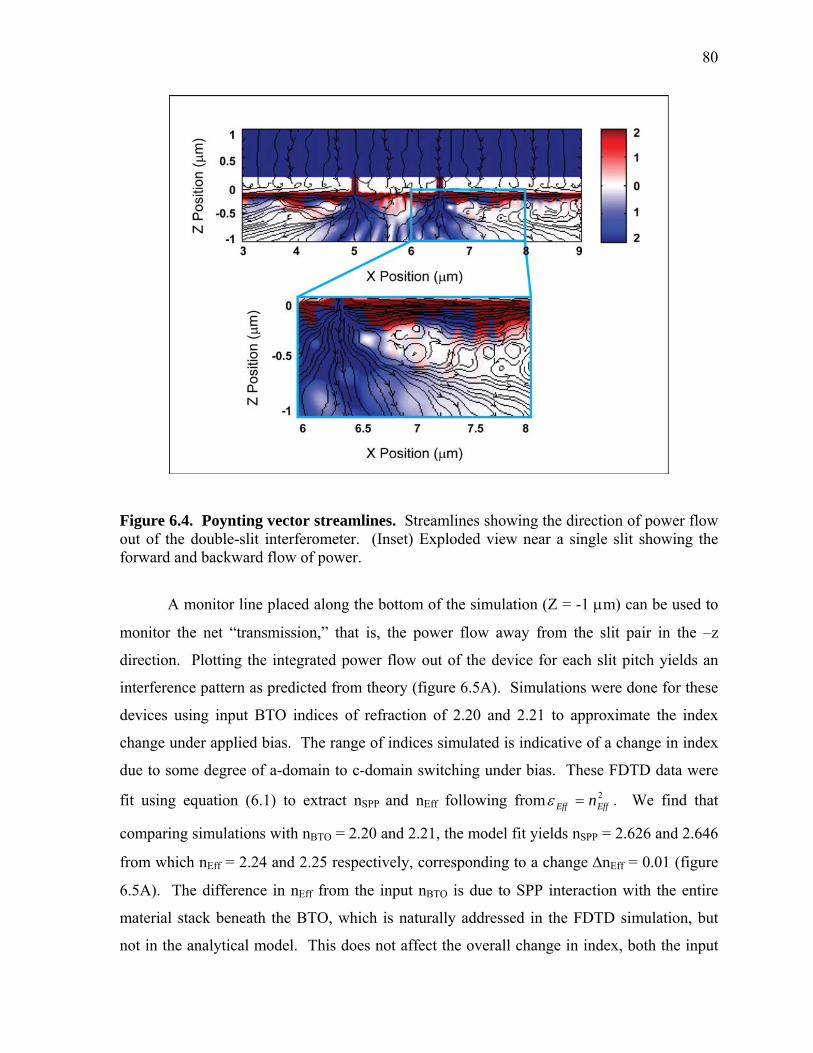
80
Figure 6.4. Poynting vector streamlines. Streamlines showing the direction of power flow out of the double-slit interferometer. (Inset) Exploded view near a single slit showing the forward and backward flow of power.
A monitor line placed along the bottom of the simulation (Z = -1 m) can be used to
monitor the net “transmission,” that is, the power flow away from the slit pair in the –z
direction. Plotting the integrated power flow out of the device for each slit pitch yields an
interference pattern as predicted from theory (figure 6.5A). Simulations were done for these
devices using input BTO indices of refraction of 2.20 and 2.21 to approximate the index
change under applied bias. The range of indices simulated is indicative of a change in index
due to some degree of a-domain to c-domain switching under bias. These FDTD data were
fit using equation (6.1) to extract nSPP and nEff following from 2EffEff n . We find that
comparing simulations with nBTO = 2.20 and 2.21, the model fit yields nSPP = 2.626 and 2.646
from which nEff = 2.24 and 2.25 respectively, corresponding to a change nEff = 0.01 (figure
6.5A). The difference in nEff from the input nBTO is due to SPP interaction with the entire
material stack beneath the BTO, which is naturally addressed in the FDTD simulation, but
not in the analytical model. This does not affect the overall change in index, both the input
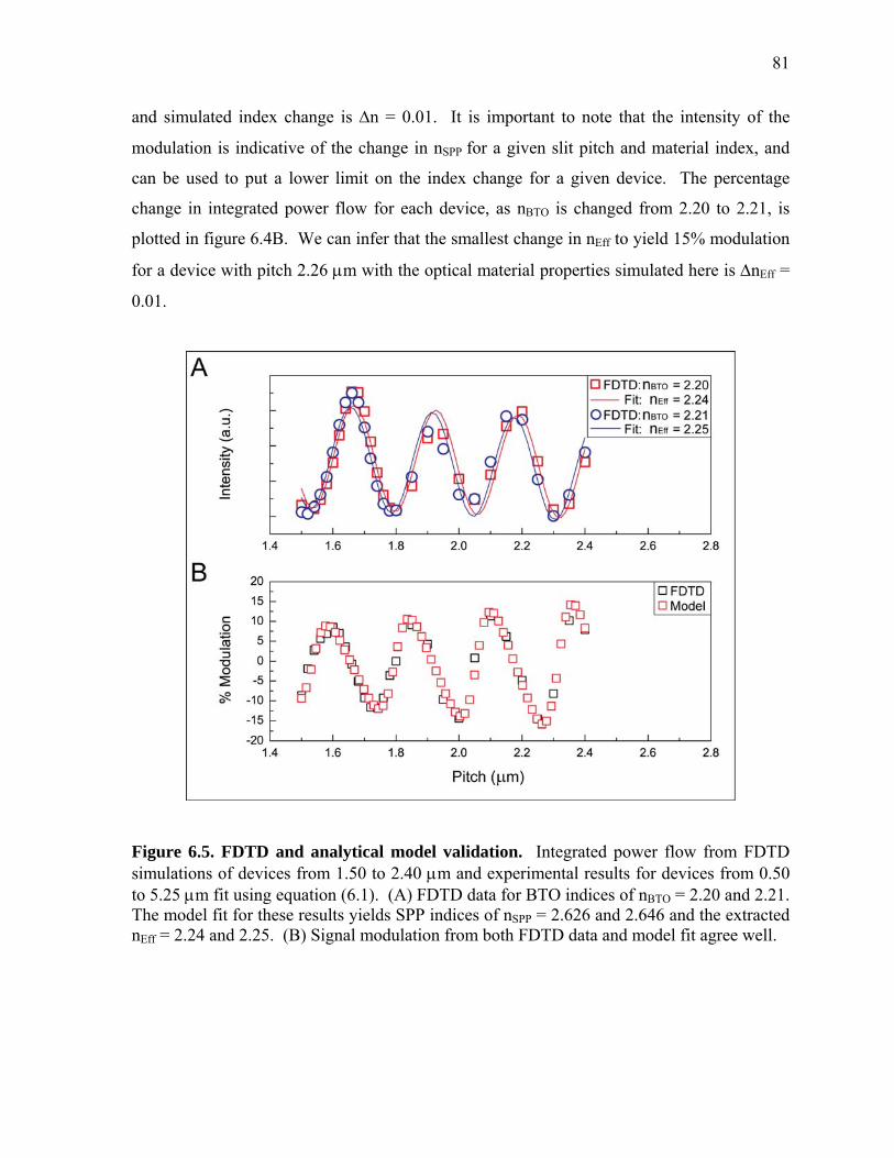
81
and simulated index change is n = 0.01. It is important to note that the intensity of the
modulation is indicative of the change in nSPP for a given slit pitch and material index, and
can be used to put a lower limit on the index change for a given device. The percentage
change in integrated power flow for each device, as nBTO is changed from 2.20 to 2.21, is
plotted in figure 6.4B. We can infer that the smallest change in nEff to yield 15% modulation
for a device with pitch 2.26 m with the optical material properties simulated here is nEff =
0.01.
Figure 6.5. FDTD and analytical model validation. Integrated power flow from FDTD simulations of devices from 1.50 to 2.40 m and experimental results for devices from 0.50 to 5.25 m fit using equation (6.1). (A) FDTD data for BTO indices of nBTO = 2.20 and 2.21. The model fit for these results yields SPP indices of nSPP = 2.626 and 2.646 and the extracted nEff = 2.24 and 2.25. (B) Signal modulation from both FDTD data and model fit agree well.
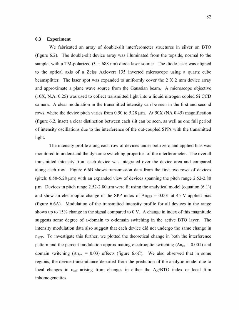
82
6.3 Experiment
We fabricated an array of double-slit interferometer structures in silver on BTO
(figure 6.2). The double-slit device array was illuminated from the topside, normal to the
sample, with a TM-polarized ( = 688 nm) diode laser source. The diode laser was aligned
to the optical axis of a Zeiss Axiovert 135 inverted microscope using a quartz cube
beamsplitter. The laser spot was expanded to uniformly cover the 2 X 2 mm device array
and approximate a plane wave source from the Gaussian beam. A microscope objective
(10X, N.A. 0.25) was used to collect transmitted light into a liquid nitrogen cooled Si CCD
camera. A clear modulation in the transmitted intensity can be seen in the first and second
rows, where the device pitch varies from 0.50 to 5.28 m. At 50X (NA 0.45) magnification
(figure 6.2, inset) a clear distinction between each slit can be seen, as well as one full period
of intensity oscillations due to the interference of the out-coupled SPPs with the transmitted
light.
The intensity profile along each row of devices under both zero and applied bias was
monitored to understand the dynamic switching properties of the interferometer. The overall
transmitted intensity from each device was integrated over the device area and compared
along each row. Figure 6.6B shows transmission data from the first two rows of devices
(pitch: 0.50-5.28 m) with an expanded view of devices spanning the pitch range 2.52-2.80
m. Devices in pitch range 2.52-2.80 m were fit using the analytical model (equation (6.1))
and show an electrooptic change in the SPP index of nSPP = 0.001 at 45 V applied bias
(figure 6.6A). Modulation of the transmitted intensity profile for all devices in the range
shows up to 15% change in the signal compared to 0 V. A change in index of this magnitude
suggests some degree of a-domain to c-domain switching in the active BTO layer. The
intensity modulation data also suggest that each device did not undergo the same change in
nSPP. To investigate this further, we plotted the theoretical change in both the interference
pattern and the percent modulation approximating electrooptic switching (neo = 0.001) and
domain switching (na-c = 0.03) effects (figure 6.6C). We also observed that in some
regions, the device transmittance departed from the prediction of the analytic model due to
local changes in nEff arising from changes in either the Ag/BTO index or local film
inhomogeneities.
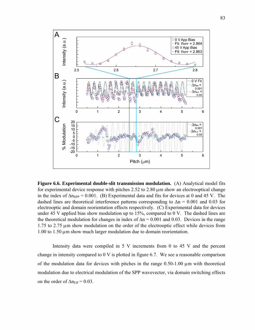
83
Figure 6.6. Experimental double-slit transmission modulation. (A) Analytical model fits for experimental device response with pitches 2.52 to 2.80 m show an electrooptical change in the index of nSPP = 0.001. (B) Experimental data and fits for devices at 0 and 45 V. The dashed lines are theoretical interference patterns corresponding to n = 0.001 and 0.03 for electrooptic and domain reorientation effects respectively. (C) Experimental data for devices under 45 V applied bias show modulation up to 15%, compared to 0 V. The dashed lines are the theoretical modulation for changes in index of n = 0.001 and 0.03. Devices in the range 1.75 to 2.75 m show modulation on the order of the electrooptic effect while devices from 1.00 to 1.50 m show much larger modulation due to domain reorientation.
Intensity data were compiled in 5 V increments from 0 to 45 V and the percent
change in intensity compared to 0 V is plotted in figure 6.7. We see a reasonable comparison
of the modulation data for devices with pitches in the range 0.50-1.00 m with theoretical
modulation due to electrical modulation of the SPP wavevector, via domain switching effects
on the order of nEff = 0.03.
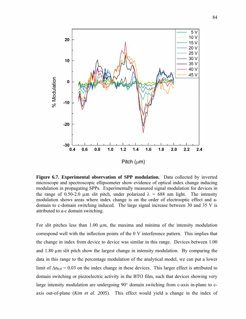
84
Figure 6.7. Experimental observation of SPP modulation. Data collected by inverted microscope and spectroscopic ellipsometer show evidence of optical index change inducing modulation in propagating SPPs. Experimentally measured signal modulation for devices in the range of 0.50-2.0 m slit pitch, under polarized = 688 nm light. The intensity modulation shows areas where index change is on the order of electrooptic effect and a-domain to c-domain switching induced. The large signal increase between 30 and 35 V is attributed to a-c domain switching.
For slit pitches less than 1.00 m, the maxima and minima of the intensity modulation
correspond well with the inflection points of the 0 V interference pattern. This implies that
the change in index from device to device was similar in this range. Devices between 1.00
and 1.80 m slit pitch show the largest change in intensity modulation. By comparing the
data in this range to the percentage modulation of the analytical model, we can put a lower
limit of nEff = 0.03 on the index change in these devices. This larger effect is attributed to
domain switching or piezoelectric activity in the BTO film, such that devices showing very
large intensity modulation are undergoing 90° domain switching from c-axis in-plane to c-
axis out-of-plane (Kim et al. 2005). This effect would yield a change in the index of
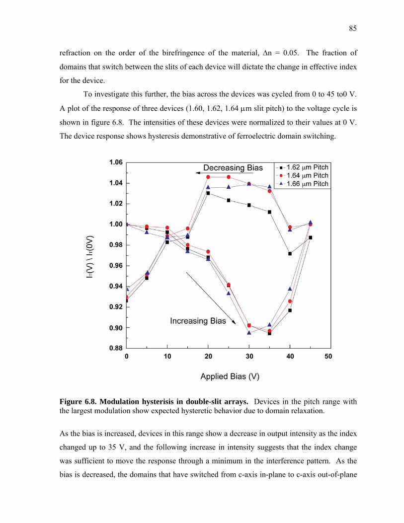
85
refraction on the order of the birefringence of the material, n = 0.05. The fraction of
domains that switch between the slits of each device will dictate the change in effective index
for the device.
To investigate this further, the bias across the devices was cycled from 0 to 45 to0 V.
A plot of the response of three devices (1.60, 1.62, 1.64 m slit pitch) to the voltage cycle is
shown in figure 6.8. The intensities of these devices were normalized to their values at 0 V.
The device response shows hysteresis demonstrative of ferroelectric domain switching.
Figure 6.8. Modulation hysterisis in double-slit arrays. Devices in the pitch range with the largest modulation show expected hysteretic behavior due to domain relaxation.
As the bias is increased, devices in this range show a decrease in output intensity as the index
changed up to 35 V, and the following increase in intensity suggests that the index change
was sufficient to move the response through a minimum in the interference pattern. As the
bias is decreased, the domains that have switched from c-axis in-plane to c-axis out-of-plane
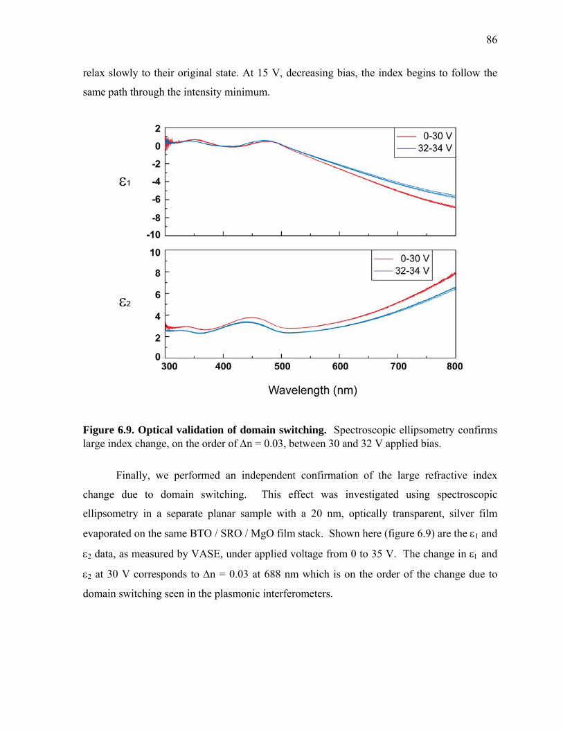
86
relax slowly to their original state. At 15 V, decreasing bias, the index begins to follow the
same path through the intensity minimum.
Figure 6.9. Optical validation of domain switching. Spectroscopic ellipsometry confirms large index change, on the order of n = 0.03, between 30 and 32 V applied bias.
Finally, we performed an independent confirmation of the large refractive index
change due to domain switching. This effect was investigated using spectroscopic
ellipsometry in a separate planar sample with a 20 nm, optically transparent, silver film
evaporated on the same BTO / SRO / MgO film stack. Shown here (figure 6.9) are the 1 and
2 data, as measured by VASE, under applied voltage from 0 to 35 V. The change in and
2 at 30 V corresponds to n = 0.03 at 688 nm which is on the order of the change due to
domain switching seen in the plasmonic interferometers.
87
6.4 Conclusions
The phenomena of SPP-mediated interference using a pair of sub-wavelength slits in
silver on BTO thin films has been investigated by a simple analytical model, full-field finite
difference simulations and experiment. Electrical modulation of the SPP wavevector was
achieved by utilizing the electrooptic effect as well as 90° domain switching in BTO. The
degree of optical switching obtained in these devices is potentially useful for designing new
plasmonic and metamaterial structures in which active oxide replaces a static dielectric
material. As photonic networks become more prevalent in chip-based microelectronic
systems, the need for active nanoscale devices is increasingly apparent. Active plasmonic
devices, based on electrooptic modulation, are well suited to fill this nanophotonic niche.

88
Chapter 7
Active Metamaterials in the Near-Infrared
In this chapter we present the first active, frequency-tunable, metamaterial devices
operating in the near-infrared spectrum from 1.5 to 5 m. These devices are based on typical
split-ring resonator (SRR) structures fabricated on the vanadium oxide (VO2) thin films
discussed previously in this thesis. Metamaterial arrays were designed, simulated, fabricated
and tested in our lab.
7.1 Introduction
Electromagnetic resonances in subwavelength metallic structures fabricated on
dielectrics can be used to engineer optical responses not found in natural materials (Enkrich
et al. 2005, Shalaev 2007, Smith et al. 2004). These “metamaterials” have reemerged from
their initial incarnation (Veselago 1968) and are currently subject to intense investigation for
their applications in super lensing (Pendry 2000), optical cloaking (Cai et al. 2007) and
negative index (Shalaev et al. 2005). Recently, active metamaterials have been demonstrated
over a narrow range around 1 THz using photoexcitation in semiconductors (Chen et al.
2006) and the metal-insulator phase transition in VO2 (Driscoll et al. 2008). Engineering
metamaterials with tunable resonances near communications wavelengths would have a
profound effect on on-chip optical devices. Here, we demonstrate frequency-tunable
metamaterials based on Ag/ and Au/VO2 hybrid structures in the near-IR range from 1.5 to 5
m. Hybrid Ag/ and Au/VO2 structures allow optical and geometrical engineering of
metamaterial devices leading to resonant peak position tuning and frequency shifts up to half
a line width.
Metamaterial designs span the electromagnetic spectrum from millimeter waves
(Smith et al. 2000) to the near-IR (Soukoulis et al. 2007). Typical metamaterials consist of
arrays of metal structures embedded in a dielectric with feature sizes much smaller than the
desired operating wavelength. In the simplest sense, each unit cell of the array is considered
to be an individual LC circuit with resonant frequency o~√ 1/(LC) (Linden et al. 2004).
SRRs are the basis for many metamaterial designs due to the ease with which they may be
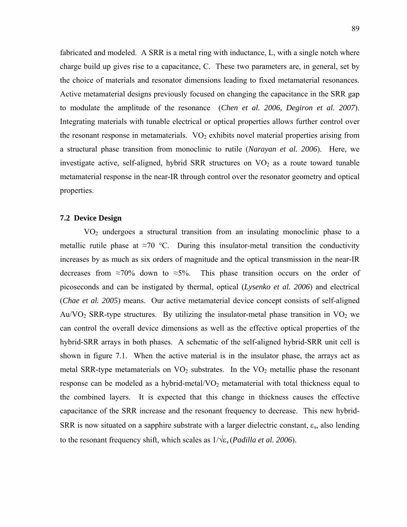
89
fabricated and modeled. A SRR is a metal ring with inductance, L, with a single notch where
charge build up gives rise to a capacitance, C. These two parameters are, in general, set by
the choice of materials and resonator dimensions leading to fixed metamaterial resonances.
Active metamaterial designs previously focused on changing the capacitance in the SRR gap
to modulate the amplitude of the resonance (Chen et al. 2006, Degiron et al. 2007).
Integrating materials with tunable electrical or optical properties allows further control over
the resonant response in metamaterials. VO2 exhibits novel material properties arising from
a structural phase transition from monoclinic to rutile (Narayan et al. 2006). Here, we
investigate active, self-aligned, hybrid SRR structures on VO2 as a route toward tunable
metamaterial response in the near-IR through control over the resonator geometry and optical
properties.
7.2 Device Design
VO2 undergoes a structural transition from an insulating monoclinic phase to a
metallic rutile phase at ≈70 °C. During this insulator-metal transition the conductivity
increases by as much as six orders of magnitude and the optical transmission in the near-IR
decreases from ≈70% down to ≈5%. This phase transition occurs on the order of
picoseconds and can be instigated by thermal, optical (Lysenko et al. 2006) and electrical
(Chae et al. 2005) means. Our active metamaterial device concept consists of self-aligned
Au/VO2 SRR-type structures. By utilizing the insulator-metal phase transition in VO2 we
can control the overall device dimensions as well as the effective optical properties of the
hybrid-SRR arrays in both phases. A schematic of the self-aligned hybrid-SRR unit cell is
shown in figure 7.1. When the active material is in the insulator phase, the arrays act as
metal SRR-type metamaterials on VO2 substrates. In the VO2 metallic phase the resonant
response can be modeled as a hybrid-metal/VO2 metamaterial with total thickness equal to
the combined layers. It is expected that this change in thickness causes the effective
capacitance of the SRR increase and the resonant frequency to decrease. This new hybrid-
SRR is now situated on a sapphire substrate with a larger dielectric constant, s, also lending
to the resonant frequency shift, which scales as 1/√s (Padilla et al. 2006).
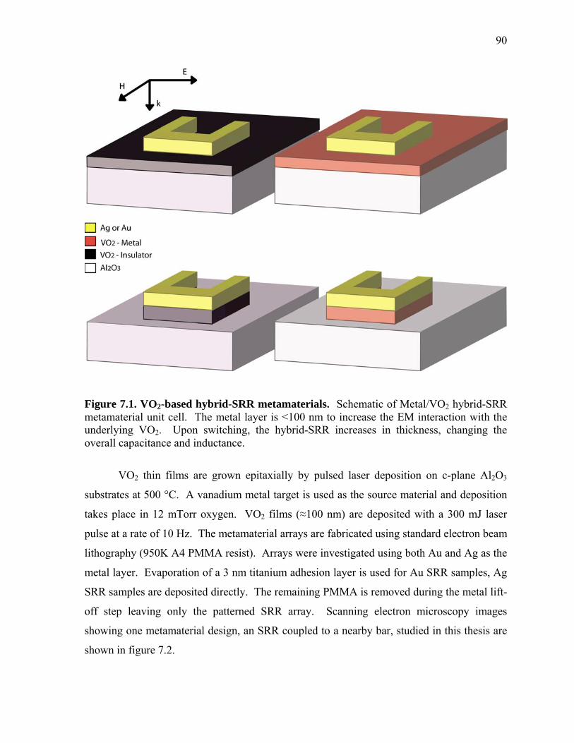
90
Figure 7.1. VO2-based hybrid-SRR metamaterials. Schematic of Metal/VO2 hybrid-SRR metamaterial unit cell. The metal layer is <100 nm to increase the EM interaction with the underlying VO2. Upon switching, the hybrid-SRR increases in thickness, changing the overall capacitance and inductance.
VO2 thin films are grown epitaxially by pulsed laser deposition on c-plane Al2O3
substrates at 500 °C. A vanadium metal target is used as the source material and deposition
takes place in 12 mTorr oxygen. VO2 films (≈100 nm) are deposited with a 300 mJ laser
pulse at a rate of 10 Hz. The metamaterial arrays are fabricated using standard electron beam
lithography (950K A4 PMMA resist). Arrays were investigated using both Au and Ag as the
metal layer. Evaporation of a 3 nm titanium adhesion layer is used for Au SRR samples, Ag
SRR samples are deposited directly. The remaining PMMA is removed during the metal lift-
off step leaving only the patterned SRR array. Scanning electron microscopy images
showing one metamaterial design, an SRR coupled to a nearby bar, studied in this thesis are
shown in figure 7.2.
91
Figure 7.2. SEM images of coupled-SRR arrays. (A) A sample metamaterial array studied in this work based on coupling the typical SRR to a nearby metal element. SRR structures show good fidelity over the entire 70 X 70 m array. Various SRR unit cell designs were studied, one such design is a typical SRR coupled to a straight bar. (B) 30 nm, (C) 60 nm, and (D) 90 nm gaps are shown. Coupled-SRR designs yield multiple resonances in the near-IR spectrum at these dimensions. Engineering the gap distances and SRR arm lengths is used to tune the resonant peaks across the near-IR spectrum.
92
7.3 Metamaterial Response in the Near-Infrared
7.3.1 Planar, VO2-Based, Hybrid-SRR Metamaterials
Metamaterial arrays are illuminated at normal incidence through a FTIR microscope
using a light source in the range of 1.5 to 8 m. The incident E-field is polarized
perpendicular to the SRR arms to efficiently couple to the capacitance inducing a circulating
current in the structure. The measured reflection spectra are normalized to the reflectivity of
an optically thick gold film. Figure 7.3 shows reflection spectra for 50 nm thick Ag SRR-
based structures on 60 nm thick VO2 thin films. These samples were heated using a
commercial heating stage add-on comprised of a silver block with a millimeter-sized aperture
milled in the center. Resonant peaks show no change as the temperature is increased from
room temperature up to 60 °C. At 65 °C the resonant reflection peaks begin to red shift
slightly and the reflectivity decreases as the VO2 thin film changes phase. The phase change
modifies the local fields in the SRR, acting like a tunable dielectric inside a capacitor. The
resonance frequency of the SRR decreases (wavelength increases) as the VO2 permittivity
increases. This is expected from the simple RLC-circuit analysis discussed previously. This
effect continues until 75 °C when the VO2 phase change is complete and the SRR array is
electrically shorted. Above the transition temperature, the sample reflectivity is dominated
by the metallic VO2 thin film. The resonances recover upon cooling below the phase
transition temperature. Coupled-SRR metamaterials were similarly investigated. The
resonant peak position in coupled-SRR can be tuned across the near-IR spectrum by
changing the distance of the strongly coupled unit (figure 7.3A-E). After investigating the
active resonant response of metal SRR arrays on planar VO2 films, these samples were
etched to create self-aligned, metal/VO2-based, hybrid SRR metamaterials.
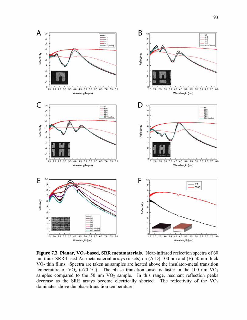
93
Figure 7.3. Planar, VO2-based, SRR metamaterials. Near-infrared reflection spectra of 60 nm thick SRR-based Au metamaterial arrays (insets) on (A-D) 100 nm and (E) 50 nm thick VO2 thin films. Spectra are taken as samples are heated above the insulator-metal transition temperature of VO2 (≈70 °C). The phase transition onset is faster in the 100 nm VO2 samples compared to the 50 nm VO2 sample. In this range, resonant reflection peaks decrease as the SRR arrays become electrically shorted. The reflectivity of the VO2 dominates above the phase transition temperature.
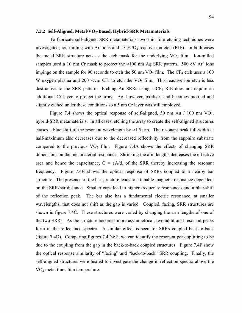
94
7.3.2 Self-Aligned, Metal/VO2-Based, Hybrid-SRR Metamaterials
To fabricate self-aligned SRR metamaterials, two thin film etching techniques were
investigated; ion-milling with Ar+ ions and a CF4/O2 reactive ion etch (RIE). In both cases
the metal SRR structure acts as the etch mask for the underlying VO2 film. Ion-milled
samples used a 10 nm Cr mask to protect the ≈100 nm Ag SRR pattern. 500 eV Ar+ ions
impinge on the sample for 90 seconds to etch the 50 nm VO2 film. The CF4 etch uses a 100
W oxygen plasma and 200 sccm CF4 to etch the VO2 film. This reactive ion etch is less
destructive to the SRR pattern. Etching Au SRRs using a CF4 RIE does not require an
additional Cr layer to protect the array. Ag, however, oxidizes and becomes mottled and
slightly etched under these conditions so a 5 nm Cr layer was still employed.
Figure 7.4 shows the optical response of self-aligned, 50 nm Au / 100 nm VO2,
hybrid-SRR metamaterials. In all cases, etching the array to create the self-aligned structures
causes a blue shift of the resonant wavelength by ≈1.5 m. The resonant peak full-width at
half-maximum also decreases due to the decreased reflectivity from the sapphire substrate
compared to the previous VO2 film. Figure 7.4A shows the effects of changing SRR
dimensions on the metamaterial resonance. Shrinking the arm lengths decreases the effective
area and hence the capacitance, C = A/d, of the SRR thereby increasing the resonant
frequency. Figure 7.4B shows the optical response of SRRs coupled to a nearby bar
structure. The presence of the bar structure leads to a tunable magnetic resonance dependent
on the SRR/bar distance. Smaller gaps lead to higher frequency resonances and a blue-shift
of the reflection peak. The bar also has a fundamental electric resonance, at smaller
wavelengths, that does not shift as the gap is varied. Coupled, facing, SRR structures are
shown in figure 7.4C. These structures were varied by changing the arm lengths of one of
the two SRRs. As the structure becomes more asymmetrical, two additional resonant peaks
form in the reflectance spectra. A similar effect is seen for SRRs coupled back-to-back
(figure 7.4D). Comparing figures 7.4D&E, we can identify the resonant peak splitting to be
due to the coupling from the gap in the back-to-back coupled structures. Figure 7.4F show
the optical response similarity of “facing” and “back-to-back” SRR coupling. Finally, the
self-aligned structures were heated to investigate the change in reflection spectra above the
VO2 metal transition temperature.

95
Figure 7.4. Self-aligned hybrid-SRR based metamaterials. 50 nm Au SRRs on 100 nm VO2 thin films (red lines) are etched by RIE to form self-aligned SRR structures (blue lines). Reflection spectra of etched structures are blue-shifted by 1.3 to 1.6 m and the line-widths narrow from ≈1.5 to 2.0 m to 500 to 700 m. (A-F) Effects of arm lengths and coupling distances are investigated in planar and etched structures.
96
7.3.3 Active, Frequency-Tunable, Hybrid-SRR Based Metamaterials
Resonant reflection response of self-aligned hybrid-SRR based metamaterials was
investigated using the heating experiment described previously for planar hybrid-SRR arrays.
Figure 7.5 shows the reflection spectra for the etched samples as the VO2 changes phase.
Compared to SRRs on planar VO2, we see resonant reflection peak wavelength shifts of 60–
110 nm upon VO2 phase transition from insulator to metal. In all cases (figures 7.5A-F), the
magnetic resonance peak shifts to lower frequency, longer wavelength. This can be
explained, using the simple RLC model, due to the increased area of the metal/VO2 hybrid-
SRR. The VO2 transition, from the insulator to the metal phase, causes the SRR thickness to
increase from the metal array thickness to the combined metal/VO2 thickness. This increase
translates to an increased area of the capacitor plates in the SRR structures and a subsequent
decrease in the resonator frequency. The increased absorption of the metal-phase VO2,
compared to Ag or Au, causes the resonant reflection peaks of the metamaterial to broaden
slightly during switching. These metamaterials represent the first generation of tunable,
VO2-based designs. To further investigate VO2 as a switching element in metamaterial
arrays, we simulated these structures using finite-difference time-domain software.
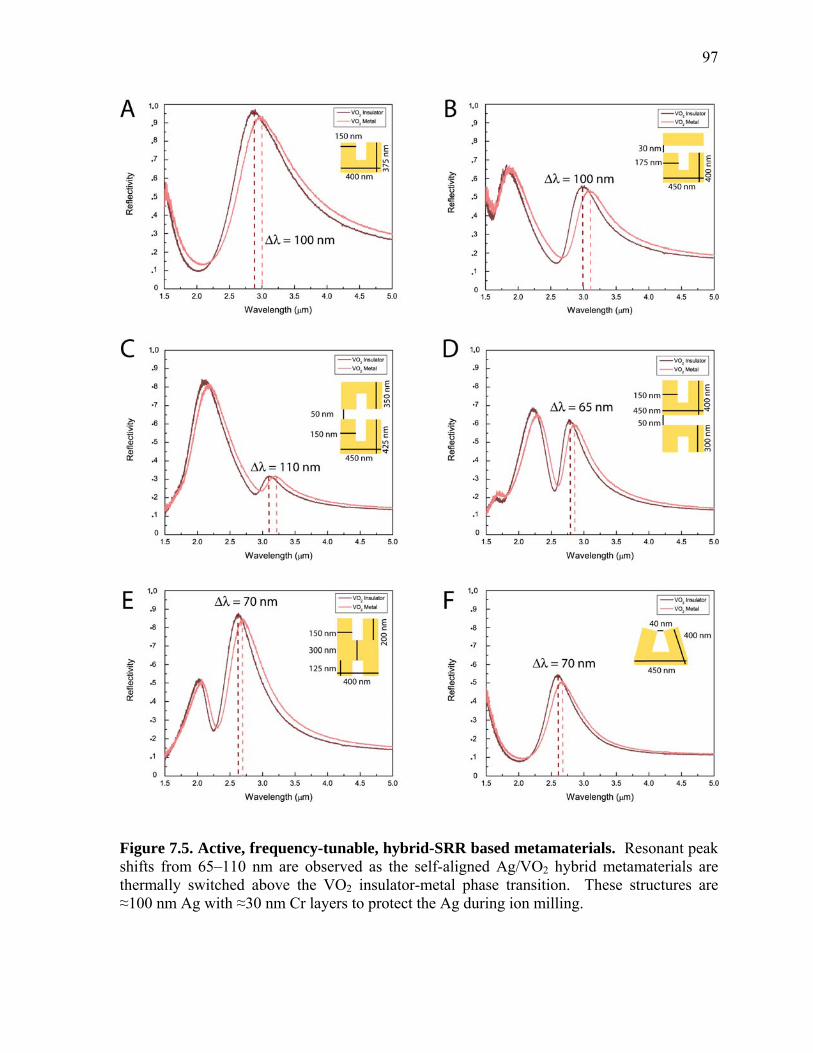
97
Figure 7.5. Active, frequency-tunable, hybrid-SRR based metamaterials. Resonant peak shifts from 65–110 nm are observed as the self-aligned Ag/VO2 hybrid metamaterials are thermally switched above the VO2 insulator-metal phase transition. These structures are ≈100 nm Ag with ≈30 nm Cr layers to protect the Ag during ion milling.
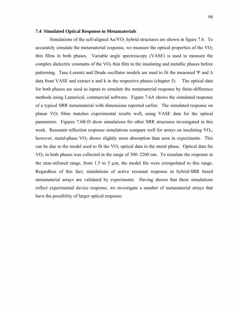
98
7.4 Simulated Optical Response in Metamaterials
Simulations of the self-aligned Au/VO2 hybrid structures are shown in figure 7.6. To
accurately simulate the metamaterial response, we measure the optical properties of the VO2
thin films in both phases. Variable angle spectroscopy (VASE) is used to measure the
complex dielectric constants of the VO2 thin film in the insulating and metallic phases before
patterning. Tauc-Lorentz and Drude oscillator models are used to fit the measured and
data from VASE and extract n and k in the respective phases (chapter 5). The optical data
for both phases are used as inputs to simulate the metamaterial response by finite-difference
methods using Lumerical, commercial software. Figure 7.6A shows the simulated response
of a typical SRR metamaterial with dimensions reported earlier. The simulated response on
planar VO2 films matches experimental results well, using VASE data for the optical
parameters. Figures 7.6B-D show simulations for other SRR structures investigated in this
work. Resonant reflection response simulations compare well for arrays on insulating VO2,
however, metal-phase VO2 shows slightly more absorption than seen in experiments. This
can be due to the model used to fit the VO2 optical data in the metal phase. Optical data for
VO2 in both phases was collected in the range of 300–2200 nm. To simulate the response in
the near-infrared range, from 1.5 to 5 m, the model fits were extrapolated to this range.
Regardless of this fact, simulations of active resonant response in hybrid-SRR based
metamaterial arrays are validated by experiments. Having shown that these simulations
reflect experimental device response, we investigate a number of metamaterial arrays that
have the possibility of larger optical response.
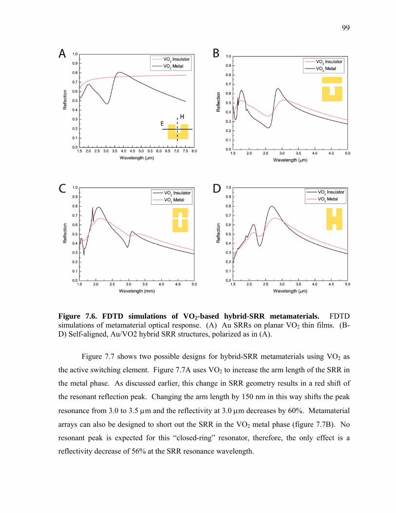
99
Figure 7.6. FDTD simulations of VO2-based hybrid-SRR metamaterials. FDTD simulations of metamaterial optical response. (A) Au SRRs on planar VO2 thin films. (B-D) Self-aligned, Au/VO2 hybrid SRR structures, polarized as in (A).
Figure 7.7 shows two possible designs for hybrid-SRR metamaterials using VO2 as
the active switching element. Figure 7.7A uses VO2 to increase the arm length of the SRR in
the metal phase. As discussed earlier, this change in SRR geometry results in a red shift of
the resonant reflection peak. Changing the arm length by 150 nm in this way shifts the peak
resonance from 3.0 to 3.5 m and the reflectivity at 3.0 m decreases by 60%. Metamaterial
arrays can also be designed to short out the SRR in the VO2 metal phase (figure 7.7B). No
resonant peak is expected for this “closed-ring” resonator, therefore, the only effect is a
reflectivity decrease of 56% at the SRR resonance wavelength.
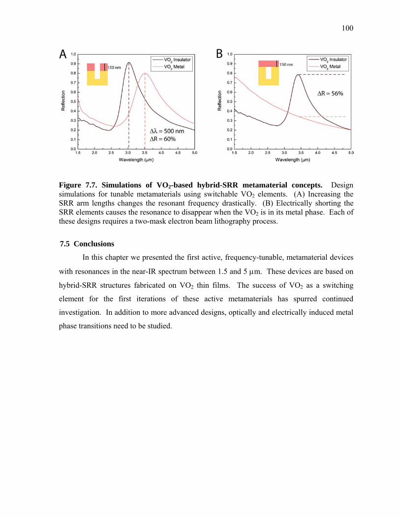
100
Figure 7.7. Simulations of VO2-based hybrid-SRR metamaterial concepts. Design simulations for tunable metamaterials using switchable VO2 elements. (A) Increasing the SRR arm lengths changes the resonant frequency drastically. (B) Electrically shorting the SRR elements causes the resonance to disappear when the VO2 is in its metal phase. Each of these designs requires a two-mask electron beam lithography process.
7.5 Conclusions
In this chapter we presented the first active, frequency-tunable, metamaterial devices
with resonances in the near-IR spectrum between 1.5 and 5 m. These devices are based on
hybrid-SRR structures fabricated on VO2 thin films. The success of VO2 as a switching
element for the first iterations of these active metamaterials has spurred continued
investigation. In addition to more advanced designs, optically and electrically induced metal
phase transitions need to be studied.
101
Chapter 8
Optical Properties of Combinatorial Metal Films
In this chapter we demonstrate the ability to fabricate metal alloy thin films with
tunable optical properties based on the alloy composition. A combinatorial approach is used
to deposit various bimetallic systems based on silver, gold and copper via magnetron
sputtering. Optical properties of Ag-Au, Ag-Cu and Au-Cu metal alloy films are
investigated with variable angle spectroscopic ellipsometry. Simulations of metal structures
are presented to illustrate the effect of tunable composition. The ability to selectively tune
the optical properties of a metallic layer has significant implications for research in
plasmonics, metamaterials and negative-index structures.
8.1 Introduction
Devices based on electromagnetic response in metals are currently attracting much
attention. Metal optics at the nanoscale has led to enhanced transmission in subwavelength
apertures (Ebbesen et al. 1998), plasmon waveguiding (Brongersma et al. 2000), cloaking
(Cai et al. 2007), negative-index materials (Lezec et al. 2007) and metamaterials (Chen et al.
2006). This wide range of applications relies on coupling of electromagnetic energy to the
collective oscillations of free electrons, or plasmons, at the interface between a dielectric and
a metal. In order to minimize the loss of energy from plasmons due to absorption, the choice
of conductive media is limited to a short list of nearly-free-electron metals such as silver,
gold, and copper; which have relatively small optical frequency electronic damping. The
study of metal-dielectric plasmonic devices has focused on designing the geometry or
varying the dielectric material composition to achieve dispersion engineering. Metal alloy
films offer a new optical engineering parameter to consider. Changing the optical properties
of the metal layer can lead to graded optical index plasmonic structures, greater tunability in
metal-insulator-metal waveguides, tunable resonances in optical metamaterials and greater
access to the negative index regime of plasmon dispersion in metal-insulator systems. It is
with this in mind that we set out to explore combinatorial synthesis of multimetal thin films.
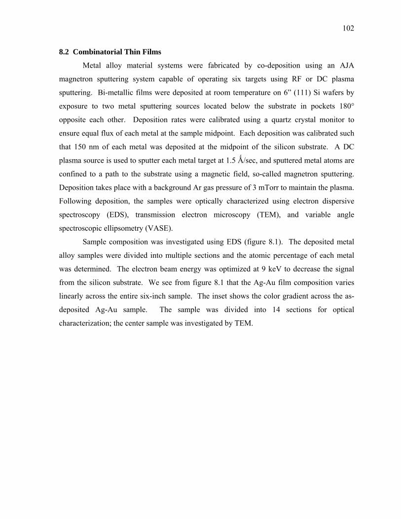
102
8.2 Combinatorial Thin Films
Metal alloy material systems were fabricated by co-deposition using an AJA
magnetron sputtering system capable of operating six targets using RF or DC plasma
sputtering. Bi-metallic films were deposited at room temperature on 6” (111) Si wafers by
exposure to two metal sputtering sources located below the substrate in pockets 180°
opposite each other. Deposition rates were calibrated using a quartz crystal monitor to
ensure equal flux of each metal at the sample midpoint. Each deposition was calibrated such
that 150 nm of each metal was deposited at the midpoint of the silicon substrate. A DC
plasma source is used to sputter each metal target at 1.5 Ǻ/sec, and sputtered metal atoms are
confined to a path to the substrate using a magnetic field, so-called magnetron sputtering.
Deposition takes place with a background Ar gas pressure of 3 mTorr to maintain the plasma.
Following deposition, the samples were optically characterized using electron dispersive
spectroscopy (EDS), transmission electron microscopy (TEM), and variable angle
spectroscopic ellipsometry (VASE).
Sample composition was investigated using EDS (figure 8.1). The deposited metal
alloy samples were divided into multiple sections and the atomic percentage of each metal
was determined. The electron beam energy was optimized at 9 keV to decrease the signal
from the silicon substrate. We see from figure 8.1 that the Ag-Au film composition varies
linearly across the entire six-inch sample. The inset shows the color gradient across the as-
deposited Ag-Au sample. The sample was divided into 14 sections for optical
characterization; the center sample was investigated by TEM.
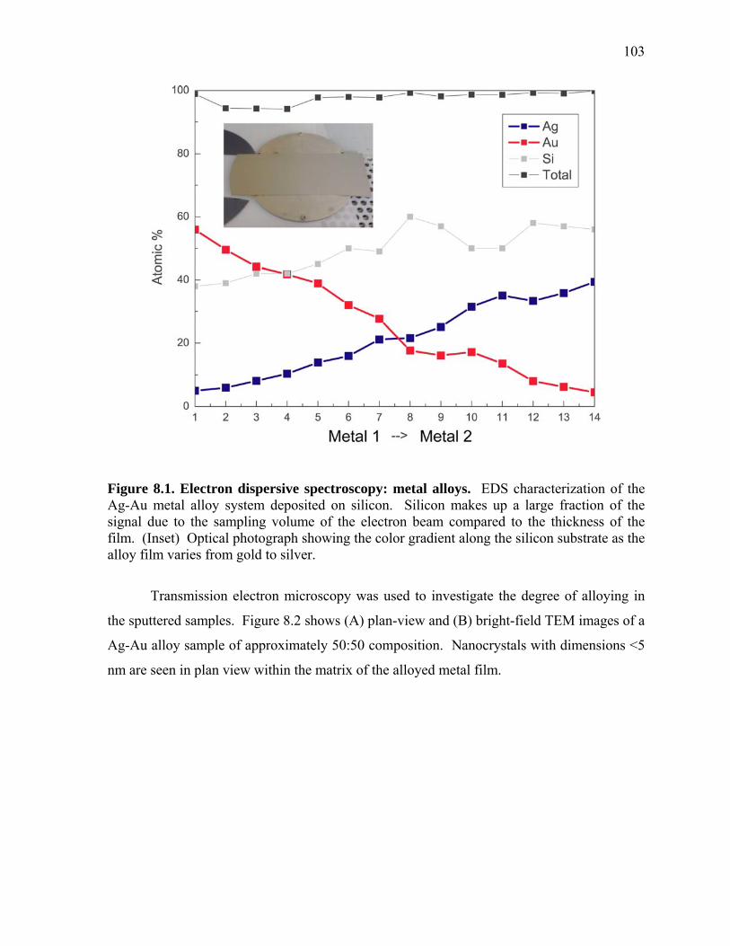
103
Figure 8.1. Electron dispersive spectroscopy: metal alloys. EDS characterization of the Ag-Au metal alloy system deposited on silicon. Silicon makes up a large fraction of the signal due to the sampling volume of the electron beam compared to the thickness of the film. (Inset) Optical photograph showing the color gradient along the silicon substrate as the alloy film varies from gold to silver.
Transmission electron microscopy was used to investigate the degree of alloying in
the sputtered samples. Figure 8.2 shows (A) plan-view and (B) bright-field TEM images of a
Ag-Au alloy sample of approximately 50:50 composition. Nanocrystals with dimensions <5
nm are seen in plan view within the matrix of the alloyed metal film.
104
Figure 8.2. Transmission electron microscopy: Ag-Au. Transmission electron microscopy images of a 50:50 Ag-Au metal alloy sample. (A) The plan-view micrograph shows the presence of some nanocrystals of Ag and Au with dimensions <5 nm in a largely alloyed matrix. (B) Bright-field microscopy shows that the film is lacking voids.
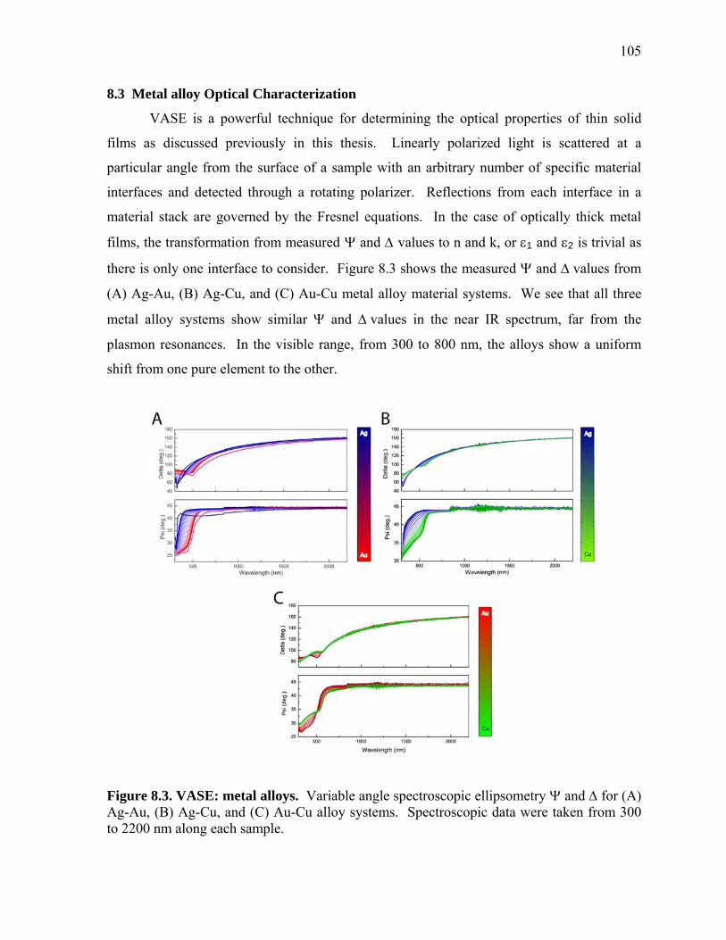
105
8.3 Metal alloy Optical Characterization
VASE is a powerful technique for determining the optical properties of thin solid
films as discussed previously in this thesis. Linearly polarized light is scattered at a
particular angle from the surface of a sample with an arbitrary number of specific material
interfaces and detected through a rotating polarizer. Reflections from each interface in a
material stack are governed by the Fresnel equations. In the case of optically thick metal
films, the transformation from measured and values to n and k, or 1 and 2 is trivial as
there is only one interface to consider. Figure 8.3 shows the measured and values from
(A) Ag-Au, (B) Ag-Cu, and (C) Au-Cu metal alloy material systems. We see that all three
metal alloy systems show similar and values in the near IR spectrum, far from the
plasmon resonances. In the visible range, from 300 to 800 nm, the alloys show a uniform
shift from one pure element to the other.
Figure 8.3. VASE: metal alloys. Variable angle spectroscopic ellipsometry and for (A) Ag-Au, (B) Ag-Cu, and (C) Au-Cu alloy systems. Spectroscopic data were taken from 300 to 2200 nm along each sample.
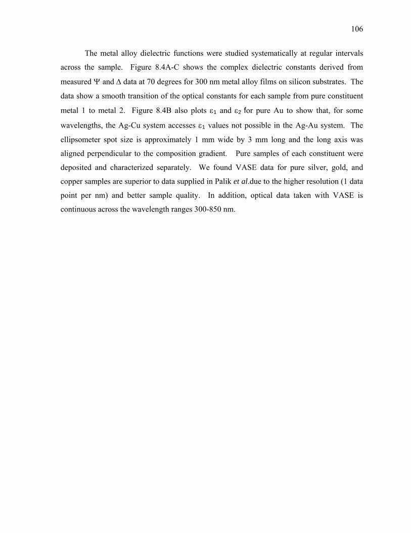
106
The metal alloy dielectric functions were studied systematically at regular intervals
across the sample. Figure 8.4A-C shows the complex dielectric constants derived from
measured and data at 70 degrees for 300 nm metal alloy films on silicon substrates. The
data show a smooth transition of the optical constants for each sample from pure constituent
metal 1 to metal 2. Figure 8.4B also plots 1 and 2 for pure Au to show that, for some
wavelengths, the Ag-Cu system accesses 1 values not possible in the Ag-Au system. The
ellipsometer spot size is approximately 1 mm wide by 3 mm long and the long axis was
aligned perpendicular to the composition gradient. Pure samples of each constituent were
deposited and characterized separately. We found VASE data for pure silver, gold, and
copper samples are superior to data supplied in Palik et al.due to the higher resolution (1 data
point per nm) and better sample quality. In addition, optical data taken with VASE is
continuous across the wavelength ranges 300-850 nm.
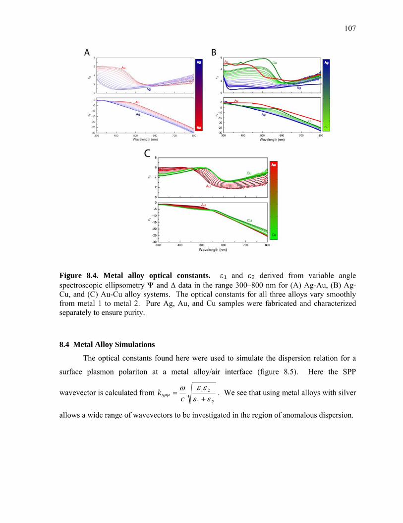
107
Figure 8.4. Metal alloy optical constants. 1 and 2 derived from variable angle spectroscopic ellipsometry and data in the range 300–800 nm for (A) Ag-Au, (B) Ag-Cu, and (C) Au-Cu alloy systems. The optical constants for all three alloys vary smoothly from metal 1 to metal 2. Pure Ag, Au, and Cu samples were fabricated and characterized separately to ensure purity.
8.4 Metal Alloy Simulations
The optical constants found here were used to simulate the dispersion relation for a
surface plasmon polariton at a metal alloy/air interface (figure 8.5). Here the SPP
wavevector is calculated from 21
21
c
kSPP . We see that using metal alloys with silver
allows a wide range of wavevectors to be investigated in the region of anomalous dispersion.
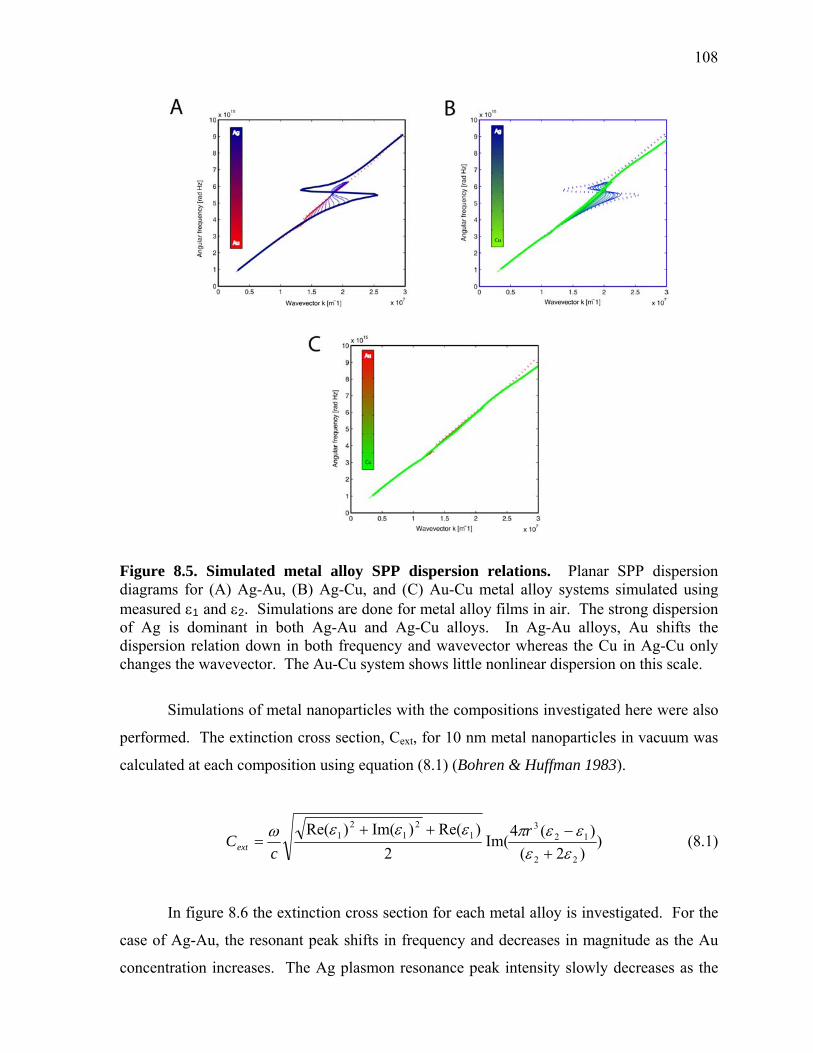
108
Figure 8.5. Simulated metal alloy SPP dispersion relations. Planar SPP dispersion diagrams for (A) Ag-Au, (B) Ag-Cu, and (C) Au-Cu metal alloy systems simulated using measured 1 and 2. Simulations are done for metal alloy films in air. The strong dispersion of Ag is dominant in both Ag-Au and Ag-Cu alloys. In Ag-Au alloys, Au shifts the dispersion relation down in both frequency and wavevector whereas the Cu in Ag-Cu only changes the wavevector. The Au-Cu system shows little nonlinear dispersion on this scale.
Simulations of metal nanoparticles with the compositions investigated here were also
performed. The extinction cross section, Cext, for 10 nm metal nanoparticles in vacuum was
calculated at each composition using equation (8.1) (Bohren & Huffman 1983).
))2(
)(4Im(
2
)Re()Im()Re(
22
123
12
12
1
r
cCext (8.1)
In figure 8.6 the extinction cross section for each metal alloy is investigated. For the
case of Ag-Au, the resonant peak shifts in frequency and decreases in magnitude as the Au
concentration increases. The Ag plasmon resonance peak intensity slowly decreases as the
109
Cu concentration increases. This is useful for tuning the nanoparticle resonance for
applications as enhanced absorbers for solar cells, plasmon waveguides and nanoantennae.
Ag-Cu nanoparticles show a broadening and decreasing of the extinction cross section.
Figure 8.6. Extinction in metal alloy nanoparticles. Extinction cross sections for 10 nm metal alloy particles in vacuum (A) Ag-Au, (B) Ag-Cu, and (C) Au-Cu. Resonances in the Ag-Au nanoparticle vary smoothly from pure Ag to pure Au. Data from Palik et al. for pure Ag are used in (A). Measured data for pure Ag and Cu plotted in (B) show a much higher extinction cross section for the pure Ag than expected from Palik et al.
8.5 Conclusions
Metal alloy systems have been realized using combinatorial techniques based on
magnetron sputtering. The optical properties of bi-metal films of Ag-Au, Ag-Cu, and Au-Cu
have been investigated using VASE and the complex dielectric constants were found to vary
systematically from pure metal 1 to pure metal 2. The largest variation of 1 and 2 for these
metals is in the visible range from 300 to 850 nm. To investigate the effects of these
variations, simulations of surface plasmon dispersion and nanoparticle extinction cross

110
section were performed. These simulations remain to be experimentally verified. In order to
fabricate samples with a single alloy composition over a large area, a MBE chamber was
built and deposition parameters explored for Ag, Au, and Cu evaporation.
111
References
Auciello, O., A. Gruverman, H. Tokumoto, S.A. Prakash, S. Aggarwal, and R. Ramesh. (1998) Nanoscale scanning force imaging of polarization phenomena in ferroelectric thin films, Mater. Res. Bull. 23.
Aydin, K. (2008) Characterization and applications of negative-index metamaterials, Ph.D. thesis, Bilkent University.
Barnes, W.L., A. Dereux, and T.W. Ebbesen. (2003) Surface plasmon subwavelength optics, Nature 424, 824-830.
Beckers, L., J. Schubert, W. Zander, J. Ziesmann, A. Eckau, P. Leinenbach, and C. Buchal. (1998) Structural and optical characterization of epitaxial waveguiding BaTiO3 thin films on MgO, J. App. Phys. 83, 3305-3310.
Bhattacharya, K., and G. Ravichandran. (2003) Ferroelectric perovskites for electromechanical actuation, Acta Mater. 51, 5941-5960.
Bhattacharya, K., and R.D. James. (2005) The material is the machine, Science 307, 53-54.
Bhushan, B., and X.D. Li. (2003) Nanomechanical characterization of solid surfaces and thin films, Int. Mater. Rev. 48, 125-164.
Bohren, C.F., and D.R. Huffman (1983) Absorption and scattering of light by small particles, Wiley, New York.
Bradley, R.M., J.M.E. Harper, and D.A. Smith. (1986) Theory of thin-film orientation by ion bombardment during deposition, J. Appl. Phys. 60, 4160-4164.
Brewer, R.T., and H.A. Atwater. (2002) Rapid biaxial texture development during nucleation of MgO thin films during ion beam-assisted deposition, Appl. Phys. Lett. 80, 3388-3390.
Brongersma, M.L., and P.G. Kik (2000) Surface plasmon nanophotonics, Springer, Dordrecht.
Burcsu, E., G. Ravichandran, and K. Bhattacharya. (2000) Large strain electrostrictive actuation in barium titanate, Appl. Phys. Lett. 77, 1698-1700.
Cai, W., U.K. Chettiar, A.V. Kildishev, and V.M. Shalaev. (2007) Optical Cloaking with Metamaterials, Nat. Phot. 1, 224-227.
112
Chae, B.G., H.T. Kim, D.H. Youn, and K.Y. Kang. (2005) Abrupt metal-insulator transition observed in VO2 thin films induced by a switching voltage pulse, Physica B 369, 76-80.
Chen, H.-T., W.J. Padilla, J.M. Zide, A.C. Gossard, A.J. Taylor, and R.D. Averitt. (2006) Active terahertz metamaterial devices, Nature 444, 597-600.
Chen, H.-T., J.F. O'Hara, A.K. Azad, A.J. Taylor, R.D. Averitt, D.B. Shrekenhamer, and W.J. Padilla. (2008) Experimental demonstration of frequency-agile terahertz metameterials, Nat. Photonics 2, 295-298.
Choi, K.J., M. Biegalski, Y.L. Li, A. Sharan, J. Schubert, R. Uecker, P. Reiche, Y.B. Chen, X.Q. Pan, V. Gopalan, L.-Q. Chen, D.G. Schlom, and C.B. Eom. (2004) Enhancement of ferroelectricity in strained BaTiO3 thin films, Science 306, 1005-1009.
Chyou, J.J., C.S. Chu, Z.H. Shih, and C.Y. Lin. (2005) Fabrication and metrology of an electro-optic polymer light modulator based on waveguide-coupled surface plasmon resonance, Opt. Eng. 44, 034001.
Damjanovic, D. (1998) Ferroelectric, dielectric and piezoelectric properties of ferroelectric thin films and ceramics, Reports on Progress in Physics 61, 1267-1324.
Degiron, A., J.J. Mock, and D.R. Smith. (2007) Modulating and tuning the response of metamaterials at the unit cell level, Optics Express 15, 1115-1127.
Dicken, M.J., K. Diest, Y.B. Park, and H.A. Atwater. (2007) Growth and optical property characterization of textured barium titanate thin films for photonic applications, J. Cryst. Growth 300, 330-335.
Dionne, J.A., L.A. Sweatlock, H.A. Atwater, and A. Polman. (2005) Planar metal plasmon waveguides: frequency-dependent dispersion, propagation, localization, and loss beyond the free electron model, Phys. Rev. B 72, 075405.
Dionne, J.A., H.J. Lezec, and H.A. Atwater. (2006) Highly confined photon transport in subwavelength metallic slot waveguides, Nano Lett. 6, 1928-1932.
Donev, E.U., J.Y. Suh, F. Villegas, R. Lopez, R.F. Haglund Jr., and L.C. Feldman. (2006) Optical properties of subwavelength hole arrays in vanadium dioxide thin films, Phys. Rev. B 73, 201401.
Dong, L., and D.J. Srolovitz. (1998) Texture development mechanisms in ion beam assisted deposition, J. Appl. Phys. 84, 5261-5269.
Driscoll, T., S. Palit, M.M. Qazilbash, M. Brehm, F. Keilmann, B.G. Chae, S.J. Yun, H.T. Kim, S.Y. Cho, N.M. Jokerst, D.R. Smith, and D.N. Basov. (2008) Dynamic tunig of an
113
infrared hybrid-metamaterial resonance using vanadium dioxide, App. Phys. Lett. 93, 024101.
Duiker, H.M., P.D. Beale, J.F. Scott, C.A.P. Dearaujo, B.M. Melnick, J.D. Cuchiaro, and L.D. McMillan. (1990) Fatigue and switching in ferroelectric memories - theory and experiment, J. Appl. Phys. 68, 5783-5791.
Ebbesen, T.W., H.J. Lezec, H.F. Ghaemi, T. Thio, and H.J. Wolff. (1998) Extraordinary optical transmission through sub-wavelength hole arrays, Nature 391, 667-669.
El-Naggar, M., D.A. Boyd, and D.G. Goodwin. (2005) Characterization of highly-oriented ferroelectric PbxBa1-xTiO3, J. Mater. Res. 20, 2969-2976.
El-Naggar, M. (2006) Textured ferroelectric thin films: synthesis, characterization, and influence of compositional grading on the dielectric behavior, Ph. D. thesis, California Institute of Technology.
Enkrich, C., M. Wegener, S. Linden, S. Burger, L. Zschiedrich, F. Schmidt, J.F. Zhou, T. Koschny, and C.M. Soukoulis. (2005) Magnetic Metamaterials at Telecommunication and Visible Frequencies, Phys. Rev. Lett. 95, 203901.
Fang, F., and W. Yang. (2002) Indentation-induced cracking and 90° domain switching pattern in barium titanate ferroelectric single crystals under different poling, Mater. Lett. 57, 198-202.
Fatuzzo, E., and W. Merz (1967) Ferroelectricity, North-Holland, Amsterdam.
Garcia-Vidal, F.J., H.J. Lezec, T.W. Ebbesen, and L. Martin-Moreno. (2003) Multiple paths to enhance optical transmission through a single subwavelength slit, Phys. Rev. Lett. 90, 213901.
Gay, G., O. Alloschery, B.V.E. Lesegno, C. O'Dwyer, J. Weiner, and H.J. Lezec. (2006) The optical response of nanostructured surfaces and the composite diffracted evanescent wave model, Nat. Phys. 2, 262-267.
Harnagea, C. (2001) Local piezoelectric response and domain structures in ferroelectric thin films investigated by voltage-modulated force microscopy, Ph.D. thesis, Martin-Luther-Universitt Hally Wittenberg.
Harnagea, C., A. Pignolet, M. Alexe, and D. Hesse. (2002) Piezoresponse scanning force microscopy: what quantitative information can we really get out of piezoresponse measurements on ferroelectric thin films, Integrated Ferroelectrics 44, 113-124.
114
Holt, M., K. Hassani, and M. Sutton. (2005) Microstructure of ferroelectric domains in BaTiO3 observed via x-ray microdiffraction, Phys. Rev. Lett. 95, 085504.
ITRS. (2007) International technology roadmap for semiconductors.
Jin, P., and S. Tanemura. (1995) Relationship between transition temperature and x in V1-
xWxO2 films deposited by dual-target magnetron sputtering, Jpn. J. Appl. Phys. 34, 2459-2460.
Kalinin, S.V., and D.A. Bonnell. (2002a) Imaging mechanism of piezoresponse force microscopy of ferroelectric surfaces, Phys. Rev. B 65, 125408.
Kalinin, S.V., C.Y. Johnson, and D.A. Bonnell. (2002b) Domain polarity and temperature induced potential inversion on the BaTiO3(100) surface, J. Appl. Phys. 91, 3816-3823.
Kalinin, S.V., A. Gruverman, and D.A. Bonnell. (2004) Quantitative analysis of nanoscale switching in SrBi2Ta2O9 thin films by piezoresponse force microscopy, Appl. Phys. Lett. 85, 795-797.
Kim, I.D., Y. Avrahami, H.L. Tuller, Y.B. Park, M.J. Dicken, and H.A. Atwater. (2005) Study of orientation effect on nanoscale polarization in BaTiO3 thin films using piezoresponse force microscopy, Appl. Phys. Lett. 86, 192907.
Kretschmann, E., and H. Raether. (1968) Radiative decay of non-radiative surface plasmons excited by light, Zeitschrift fur Naturforschung 23A.
Krulevitch, P., A.P. Lee, P.B. Ramsey, J.C. Trevino, J. Hamilton, and M.A. Northrup. (1996) Thin film shape memory alloy microactuators, J. MEMS 5, 270-282.
Kwak, B.S., K. Zhang, E.P. Boyd, A. Erbil, and B.J. Wilkens. (1991) Metalorganic chemical vapor deposition of BaTiO3 thin films, J. Appl. Phys. 69, 767-772.
Lalanne, P., J.P. Hugonin, and J.C. Roier. (2005) Theory of surface plasmon generation at nanoslit apertures, Phys. Rev. Lett. 95, 263902.
Lappalainen, J., S. Heinilehto, S. Saukko, V. Lantto, and H. Jantunen. (2008) Microstructure dependent switching properties of VO2 thin films, Sensor. Actuat. A 142, 250-255.
Lemoine, C., B. Gilbert, B. Michaux, J.P. Pirard, and A.J. Lecloux. (1994) Synthesis of barium titanate by the sol-gel process, J. Non-Cryst. Solids 175, 1-13.
Lezec, H.J., A. Degiron, E. Devaux, R.A. Linke, L. Martin-Moreno, F.J. Garcia-Vidal, and T.W. Ebbesen. (2002) Beaming light from a subwavelength aperture, Science 297, 820-822.
115
Lezec, H.J., and T. Thio. (2004) Diffracted evaescent wave model for enhanced and suppressed optical transmission through sub-wavelength hole arrays, Opt. Exp. 12, 3629-3651.
Lezec, H.J., J.A. Dionne, and H.A. Atwater. (2007) Negative Refraction at Visible Frequencies, Science 316, 3.
Li, J.Y., R.C. Rogan, E. Ustundag, and K. Bhattacharya. (2005) Domain switching in polycrystalline ferroelectric ceramics, Nat. Mater. 4, 776-781.
Li, X.D., and B. Bhushan. (2002) A review of nanoindentation continuous stiffness measurement technique and its applications, Mater. Charact. 48, 11-36.
Li, X.D., H.S. Gao, C.J. Murphy, and K.K. Caswell. (2003) Nanoindentation of silver nanowires, Nano Lett. 3, 1495-1498.
Li, Z., C.M. Foster, X.H. Dai, S.K. Chan, and D.J. Lam. (1992) Piezoelectrically-induced switching of 90° domains in tetragonal BaTiO3 and PbTiO3 investigated by micro-Raman spectroscopy, J. Appl. Phys. 71, 4481-4486.
Linden, S., C. Enkrich, M. Wegener, J. Zhou, T. Koschny, and C.M. Soukoulis. (2004) Magnetic response of metamaterials at 100 terahertz Science 306, 1351-1353.
Lipinsky, T., J. Schubert, and C. Buchal. (2005) Crack-free BaTiO3 films on Si with SiO2, MgO, or Al2O3 buffer layers, J. Opt. Soc. Am. B 22, 913-916.
Lisoni, J.G., M. Siegert, C.H. Lei, W. Biegel, J. Schubert, W. Zander, and C. Buchal. (2001) The growth of MgO buffer layers on sapphire for the epitaxy of BaTiO3 optical thin films, Thin Solid Films 389, 219-226.
Lysenko, S., A.J. Rua, V. Vikhnin, J. Jimenez, F. Fernandez, and H. Liu. (2006) Light-induced ultrafast phase transitions in VO2 thin film, App. Surf. Sci. 252, 5512-5515.
Maier, S.A., P.G. Kik, H.A. Atwater, S. Meltzer, E. Harel, B.E. Koel, and A.A.G. Requicha. (2003) Local detection of electromagnetic energy transport below the diffraction limit in metal nanoparticle plasmon waveguides, Nat. Mater. 2, 229-232.
McKee, R.A., F.J. Walker, J.R. Conner, E.D. Specht, and D.E. Zelmon. (1991) Molecular beam epitaxy growth of epitaxial barium silicide, barium oxide, and barium titanate on silicon, Appl. Phys. Lett. 59, 782-784.
Narayan, J., and V.M. Bhosle. (2006) Phase transition and critical issues in structure-property correlations of vanadium oxide, J. Appl. Phys. 100, 103524.
116
Nye, J. (1957) Physical properties of crystals, Oxford University Press, Oxford.
Oliver, W.C., and G.M. Pharr. (1992) An improved technique for determining hardness and elastic modulus using load and displacement sensing indentation experiments, J. Mater. Res. 7, 1564-1583.
OptiFDTD. (2005) Finite-Difference Time-Domain Simulation Design Software Optiwave Systems Inc.
Pacifici, D., H.J. Lezec, and H.A. Atwater. (2007) All-optical modulation by plasmonic excitation of CdSe quantum dots, Nat. Photonics 1, 402-406.
Pacifici, D., H.J. Lezec, J. Weiner, and H.A. Atwater. (2008) Quantitative determination of optical transmission through sub-wavelength slit arrays in Ag films, Phys. Rev. B 77, 115411.
Padilla, W.J., D.N. Basov, and D.R. Smith. (2006) Negative refractive index metamaterials, Materials Today 9, 28-35.
Park, S.E., S. Wada, L.E. Cross, and T.R. Shrout. (1999) Crystallographically engineered BaTiO3 single crystals for high-performance piezoelectrics, J. Appl. Phys. 86, 2746-2750.
Park, Y.B., J.L. Ruglovsky, and H.A. Atwater. (2004) Microstructure and properties of single crystal BaTiO3 thin films synthesized by ion implantation-induced layer transfer, Appl. Phys. Lett. 85, 455-457.
Pendry, J.B., A.J. Holden, D.J. Robbins, and W.J. Stewart. (1999) Magnetism from conductors and enhanced nonlinear phenomena, IEEE Trans. Microw. Theory 47, 2075-2084.
Pendry, J.B. (2000) Negative Refraction Makes a Perfect Lens, Phys. Rev. Lett. 85, 3966-3969.
Petraru, A., J. Schubert, M. Schmid, and C. Buchal. (2002) Ferroelectric BaTiO3 thin-film optical waveguide modulators, Appl. Phys. Lett. 81, 1375-1377.
Petraru, A., J. Schubert, M. Schmid, O. Trithaveesak, and C. Buchal. (2003) Integrated optical Mach-Zehnder modulator based on polycrystalline BaTiO3, Opt. Lett. 15, 2527-2529.
Raether, H. (1988) Surface plasmons on smooth and rough surfaces and on gratings, Springer, Berlin.
Rakic, A.D., A.B. Djurisic, J.M. Elazar, and M.L. Majewski. (1998) Optical properties of metallic films for vertical-cavity optoelectronic devices, Appl. Opt. 37, 5271-5283.
117
Ramesh, R., W.K. Chan, B. Wilkens, B. Gilchrist, T. Sands, J.M. Tarascon, V.G. Keramidas, D.K. Fork, J. Lee, and A. Safari. (1992) Fatigue and retention in ferroelectric Y-Ba-Cu-O/Pb-Zr-Ti-O/Y-Ba-Cu-O heterostructures, Appl. Phys. Lett. 61, 1537-1539.
Ressler, K.G., N. Sonnenberg, and M.J. Cima. (1997) Mechanism of biaxial alignment of oxide thin films during ion-beam assisted deposition, J. Am. Ceram. Soc. 80, 2637-2648.
Rogan, R.C., N. Tamura, G.A. Swift, and E. Ustundag. (2003) Direct measurement of triaxial strain fields around ferroelectric domains using x-ray microdiffraction, Nat. Mater. 2, 379-381.
Ruglovsky, J.L. (2007) Correlating microscopic ferroelectric properties and macroscopic thin film device performance, Ph.D. thesis, California Institute of Technology.
Saleh, B.E.A., and M.C. Teich (1991) Fundamentals of photonics, Wiley, New York.
Schlom, D.G., J.H. Haeni, J. Lettieri, C.D. Theis, W. Tian, J.C. Jiang, and X.Q. Pan. (2001) Oxide nano-engineering using MBE, Mat. Sci. Eng. B 87, 282-291.
Schouten, H.F., N. Kuzmin, G. Dubois, T.D. Visser, G. Gbur, P.F.A. Alkemade, H. Blok, G.W. 'tHooft, D. Lenstra, and E.R. Eliel. (2005) Plasmon-assisted two-slit transmission: Young's experiment revisited, Phys. Rev. Lett. 94, 053901.
Scott, J.F., C.A. Araujo, B.M. Melnick, L.D. McMillan, and R. Zuleeg. (1991) Quantitative measurement of space-charge effects in lead zirconate-titanate memories, J. Appl. Phys. 70, 382-388.
Scott, J.F. (2000) Ferroelectric memories, Springer, Berlin.
Shalaev, V.M., W. Cai, U.K. Chettiar, H.-K. Yuan, A.K. Sarychev, V.P. Drachev, and A.V. Kildishev. (2005) Negative index of refraction in optical metamaterials, Opt. Lett. 30, 3356-3358.
Shalaev, V.M. (2007) Optical negative-index metamaterials, Nat. Phot. 1, 41-47.
Smith, D.A., J.B. Pendry, and M.C.K. Wiltshire. (2004) Metamaterials and Negative Refractive Index, Science 305, 788-792.
Smith, D.R., W.J. Padilla, D.C. Vier, S.C. Nemat-Nasser, and S. Schultz. (2000) Composite medium with simultaneously negative permeability and permittivity, Phys. Rev. Lett. 84, 4184-4187.
Soukoulis, C.M., S. Linden, and M. Wegener. (2007) Negative Refractive Index at Optical Wavelengths, Science 315, 47-49.
118
Stavistki, N., V. Lyahovitskaya, J. Nair, I. Zon, R. Popovitz-Biro, E. Wachtel, Y. Feldman, and I. Lubomirsky. (2002) Substrate-free crystallization of distorted hexagonal barium titanate thin films, Appl. Phys. Lett. 81, 4177-4179.
Suh, J.Y., R. Lopez, L.C. Feldman, and R.F. Haglund Jr. (2004) Semiconductor to metal phase transition in the nucleation and growth of VO2 nanoparticles and thin films, J. Appl. Phys. 96, 1209-1213.
Sweatlock, L.A., S.A. Maier, H.A. Atwater, J.J. Penninkhof, and A. Polman. (2005) Highly confined electromagnetic fields in arrays of strongly coupled Ag nanoparticles, Phys. Rev. B 71, 235408.
Tang, P., D.J. Towner, A.L. Meier, and B.W. Wessels. (2003) Polarisation-insensitive Si3N4 strip-loaded BaTiO3 thin-film waveguide with low propagation losses, Electron. Lett. 39, 1651-1652.
Tang, P., D.J. Towner, T. Hamano, A.L. Meier, and B.W. Wessels. (2004a) Electrooptic modulation up to 40 GHz in a barium titanate thin film waveguide modulator, Opt. Exp. 12, 5962-5967.
Tang, P., D.J. Towner, A.L. Meier, and B.W. Wessels. (2004b) Low-voltage, polarization-insensitive, electro-optic modulator based on a polydomain barium titanate thin film, Appl. Phys. Lett. 85, 4615-4617.
Theis, C.D., and D.G. Schlom. (1996) Cheap and stable titanium source for use in oxide molecular beam epitaxy systems, J. Vac. Sci. Technol. A 14, 2677-2679.
Thio, T., K.M. Pellerin, R.A. Linke, H.J. Lezec, and T.W. Ebbesen. (2001) Enhanced light transmission through a single subwavelength aperture, Opt. Lett. 26, 1972-1974.
Veselago, V.G. (1968) The electrodynamics of substances with simultaneously negative values of permittivity and permeability, Sov. Phys. Usp. 10, 504-509.
Wang, C.P., K.B. Do, M.R. Beasley, T.H. Geballe, and R.H. Hammond. (1997) Deposition of in-plane textured MgO on amorphous Si3N4 substrates by ion-beam-assisted deposition and comparisons with ion-beam-assisted deposited yttria-stabilized-zirconia, Appl. Phys. Lett. 71, 2955-2957.
Wei, Q.H., K.H. Su, S. Durant, and X. Zhang. (2004) Plasmon resonance of finite one-dimensional Au nanoparticle chains, Nano Lett. 4, 1067-1071.
Wills, L.A., B.W. Wessels, D.S. Richeson, and T.J. Marks. (1992) Epitaxial growth of BaTiO3 thin films by organometallic chemical vapor deposition, Appl. Phys. Lett. 60, 41-43.
119
Xu, Z.H., and D. Rowcliffe. (2004) Finite element analysis of substrate effects on indentation behaviour of thin films, Thin Solid Films 447, 399-405.
Xu, Z.H., and X.D. Li. (2006) Sample size effect on nanoindentation of micro-/nanostructures, Acta Mater. 54, 1699-1703.
Yu, L.S., J.M.E. Harper, Cuomo, J. J., and D.A. Smith. (1985) Alignment of thin films by glancing angle ion bombardment during deposition, Appl. Phys. Lett. 47, 932-933.
Zeng, H.R., H.F. Yu, R.Q. Chu, G.R. Li, H.S. Luo, and Q.R. Yin. (2004) Domain orientation imaging of PMN–PT single crystals by vertical and lateral piezoresponse force microscopy, J. Cryst. Growth 267, 194-198.
Zgonik, M., P. Bernasconi, M. Duelli, R. Schlesser, and P. Gunter. (1994) Dielectric, elastic, piezoelectric, electro-optic, and elasto-optic tensors of BaTiO3 crystals, Phys. Rev. B 50, 5941-5949.