nanophotonics-biological-sensing (22)
TRANSCRIPT
Department of Physics
Imperial College London
Nanophotonics for Biological Sensing and HealthScreening using Terahertz Radiation
Aoife McDonald-Bowyer
supervised byProf. S.A. Maier
June 27, 2016
Nanophotonics for biological sensing and health screening with terahertz
radiation
Aoife McDonald-Bowyer
Department of Physics, Imperial College London
June 27, 2016
Abstract
The terahertz region of the electromagnetic spectrum has long been referred to as the ‘terahertz gap’ due to thelack of technological advancement in this area. It’s enigmatic nature arises from the fact that the frequency is toohigh for electronic devices to operate, but too low for optical devices. In this essay, the unique response exhibited bybiological molecules to terahertz radiation is outlined, and with this it’s applications in biological sensing explored.Additionally, various attempts at bridging the terahertz gap have been investigated. They begin with the advent of theAuston switch, and developments in increasing the emission from these with semiconductor technology and geometricaloptimisation. Attempts at bridging the gap from the higher frequency side is then explored. The difficulty with thislies fundamentally with the impossibility of conventionally imaging below the diffraction limit of light. A method for‘breaking’ the diffraction limit is outlined, and with this the necessity for half spaces bounded by a surface, realised.This in turn introduces the field of Nanophotonics and Photonics, with emphasis on the use metamaterials in guidinghighly confined surface terahertz waves. The application of periodically corrugated perfectly conducting surfaces forguiding strongly confined waves in the terahertz regime is explored, and it’s unique applications in broadband sensingsummarised.
Introduction
Physics has become an integral part of medical imaging re-
search since the discovery of X-rays by Rontgen in 1895[1].From Magnetic Resonance Imaging (MRI) to Computed To-mography (CT), radiologists and doctors now have a wealthof tools to aid patient diagnoses. However, many imagingtechniques such as X-Ray and CT utilise ionising radiation.Together with the strong magnetic fields employed in MRI,current imaging techniques pose a significant risk to many
aspects of human health [2]. Even ultrasound imaging, mostcommonly known for imaging unborn feotuses, can produce
damaging thermal effects on immature human cells[3].
Minimising the amount of radiation exposure is thusan important criterion in the development of new medi-cal imaging techniques. As a result, the field of researchinto utilising electromagnetic (EM) radiation in the tera-hertz regime has emerged and made significant advances inrecent years.
The terahertz (THz) regime is loosely defined as thesection of the electromagnetic spectrum of frequency 0.3×10¹²− 3× 10¹² Hz[4]. They are also referred to as T-waves,or sub-millimeter waves due to their wavelength. There areseveral features unique to T-waves that make them suit-able for medical imaging. Photons in the terahertz regime
have relatively low energy[5], meaning they are incapable ofionising atoms and causing chemical damage to molecules.Additionally, THz radiation has been shown to excite manyinter-molecular interactions of biological molecules. Kindt
et al.[6] confirmed that the changing rotational and vibra-tional modes of polar diatomic molecules caused character-istic absorption lines in the THz region of the spectrum.This sensitivity of THz radiation to polar substances, andin particular biomolecules, presents it as an attractive tool
for medical imaging. Furthermore, due to the high watercontent of biological tissue, and the susceptibility of THz ra-diation to it, this could also lead to higher soft tissue imagecontrast than other techniques.
The terahertz region of the EM spectrum has long beenreferred to as the ‘THz gap’, due to the lack of technolog-ical advances using this type of radiation. It is a particu-larly vexing part of the spectrum, in that it is of too higha frequency for electronic devices to operate, but too low afrequency for optical devices. It is where, up until recently,no semiconductor technology has been able to efficientlyconvert electrical power into electromagnetic radiation.
Transistors are the backbone of devices that operate atthe lower end of the EM spectrum and produce microwaves.They are based on electron transport and have an upperworking limit of 300 GHz (they are actually most practi-
cal at 50 GHz)[12]. Any attempt to produce higher fre-quencies, encroaching on the THz region, incur such powerlosses that the devices are so inefficient they are no longeruseful. At the other end, alternative semiconductor devicesas well as optical and quantum pumped lasers can produceradiation to a lower limit of 10 micrometers. Between theoperating limits of these two technologies lies the terahertzgap. Bridging it involves the development of compact yetpowerful sources and detectors.
To fully appreciate the challenges that research into thisfield poses, an understanding of the underlying physicalprinciples is necessary. These ideas are encapsulated inelectromagnetic theory, solid state physics and plasmonics.These will be sufficiently explained at appropriate pointsthroughout this essay.
1
Solid-State Devices
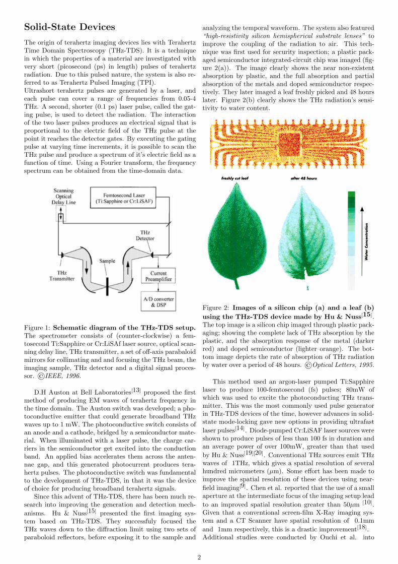
The origin of terahertz imaging devices lies with TerahertzTime Domain Spectroscopy (THz-TDS). It is a techniquein which the properties of a material are investigated withvery short (picosecond (ps) in length) pulses of terahertzradiation. Due to this pulsed nature, the system is also re-ferred to as Terahertz Pulsed Imaging (TPI).Ultrashort terahertz pulses are generated by a laser, andeach pulse can cover a range of frequencies from 0.05-4THz. A second, shorter (0.1 ps) laser pulse, called the gat-ing pulse, is used to detect the radiation. The interactionof the two laser pulses produces an electrical signal that isproportional to the electric field of the THz pulse at thepoint it reaches the detector gates. By executing the gatingpulse at varying time increments, it is possible to scan theTHz pulse and produce a spectrum of it’s electric field as afunction of time. Using a Fourier transform, the frequencyspectrum can be obtained from the time-domain data.
Figure 1: Schematic diagram of the THz-TDS setup.The spectrometer consists of (counter-clockwise) a fem-tosecond Ti:Sapphire or Cr:LiSAf laser source, optical scan-ning delay line, THz transmitter, a set of off-axis parabaloidmirrors for collimating and and focusing the THz beam, theimaging sample, THz detector and a digital signal proces-sor. ©IEEE, 1996.
D.H Auston at Bell Laboratories[13] proposed the firstmethod of producing EM waves of terahertz frequency inthe time domain. The Auston switch was developed; a pho-toconductive emitter that could generate broadband THzwaves up to 1 mW. The photoconductive switch consists ofan anode and a cathode, bridged by a semiconductor mate-rial. When illuminated with a laser pulse, the charge car-riers in the semiconductor get excited into the conductionband. An applied bias accelerates them across the anten-nae gap, and this generated photocurrent produces tera-hertz pulses. The photoconductive switch was fundamentalto the development of THz-TDS, in that it was the deviceof choice for producing broadband terahertz signals.
Since this advent of THz-TDS, there has been much re-search into improving the generation and detection mech-
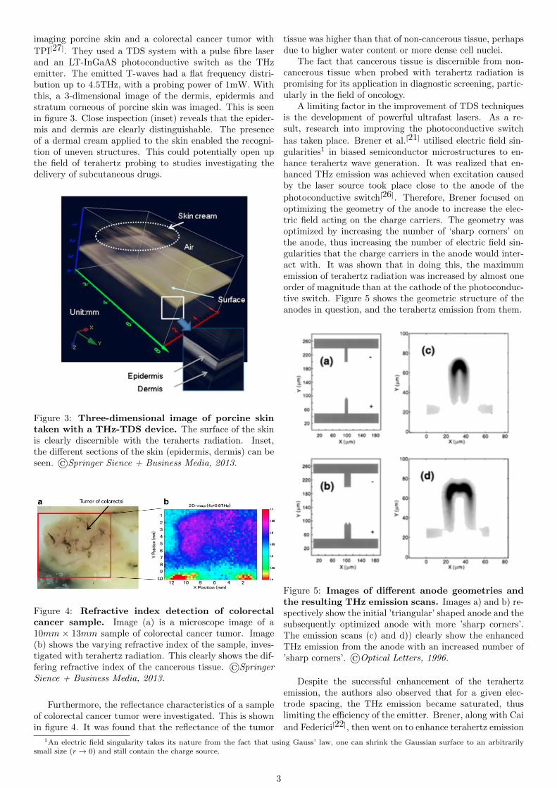
anisms. Hu & Nuss[15] presented the first imaging sys-tem based on THz-TDS. They successfuly focused theTHz waves down to the diffraction limit using two sets ofparaboloid reflectors, before exposing it to the sample and
analyzing the temporal waveform. The system also featured“high-resistivity silicon hemispherical substrate lenses” toimprove the coupling of the radiation to air. This tech-nique was first used for security inspection; a plastic pack-aged semiconductor integrated-circuit chip was imaged (fig-ure 2(a)). The image clearly shows the near non-existentabsorption by plastic, and the full absorption and partialabsorption of the metals and doped semiconductor respec-tively. They later imaged a leaf freshly picked and 48 hourslater. Figure 2(b) clearly shows the THz radiation’s sensi-tivity to water content.
Figure 2: Images of a silicon chip (a) and a leaf (b)
using the THz-TDS device made by Hu & Nuss[15].The top image is a silicon chip imaged through plastic pack-aging; showing the complete lack of THz absorption by theplastic, and the absorption response of the metal (darkerred) and doped semiconductor (lighter orange). The bot-tom image depicts the rate of absorption of THz radiationby water over a period of 48 hours. ©Optical Letters, 1995.
This method used an argon-laser pumped Ti:Sapphirelaser to produce 100-femtosecond (fs) pulses; 80mW ofwhich was used to excite the photoconducting THz trans-mitter. This was the most commonly used pulse generatorin THz-TDS devices of the time, however advances in solid-state mode-locking gave new options in providing ultrafast
laser pulses[14]. Diode-pumped Cr:LiSAF laser sources wereshown to produce pulses of less than 100 fs in duration andan average power of over 100mW, greater than that used
by Hu & Nuss[19][20]. Conventional THz sources emit THzwaves of 1THz, which gives a spatial resolution of severalhundred micrometers (µm). Some effort has been made toimprove the spatial resolution of these devices using near-
field imaging[9]. Chen et al. reported that the use of a smallaperture at the intermediate focus of the imaging setup lead
to an improved spatial resolution greater than 50µm [10].Given that a conventional screen-film X-Ray imaging sys-tem and a CT Scanner have spatial resolution of 0.1mm
and 1mm respectively, this is a drastic improvement[18].Additional studies were conducted by Ouchi et al. into
2
imaging porcine skin and a colorectal cancer tumor with
TPI[27]. They used a TDS system with a pulse fibre laserand an LT-InGaAS photoconductive switch as the THzemitter. The emitted T-waves had a flat frequency distri-bution up to 4.5THz, with a probing power of 1mW. Withthis, a 3-dimensional image of the dermis, epidermis andstratum corneous of porcine skin was imaged. This is seenin figure 3. Close inspection (inset) reveals that the epider-mis and dermis are clearly distinguishable. The presenceof a dermal cream applied to the skin enabled the recogni-tion of uneven structures. This could potentially open upthe field of terahertz probing to studies investigating thedelivery of subcutaneous drugs.
Figure 3: Three-dimensional image of porcine skintaken with a THz-TDS device. The surface of the skinis clearly discernible with the teraherts radiation. Inset,the different sections of the skin (epidermis, dermis) can beseen. ©Springer Sience + Business Media, 2013.
Figure 4: Refractive index detection of colorectalcancer sample. Image (a) is a microscope image of a10mm × 13mm sample of colorectal cancer tumor. Image(b) shows the varying refractive index of the sample, inves-tigated with terahertz radiation. This clearly shows the dif-fering refractive index of the cancerous tissue. ©SpringerSience + Business Media, 2013.
Furthermore, the reflectance characteristics of a sampleof colorectal cancer tumor were investigated. This is shownin figure 4. It was found that the reflectance of the tumor
tissue was higher than that of non-cancerous tissue, perhapsdue to higher water content or more dense cell nuclei.
The fact that cancerous tissue is discernible from non-cancerous tissue when probed with terahertz radiation ispromising for its application in diagnostic screening, partic-ularly in the field of oncology.
A limiting factor in the improvement of TDS techniquesis the development of powerful ultrafast lasers. As a re-sult, research into improving the photoconductive switch
has taken place. Brener et al.[21] utilised electric field sin-gularities1 in biased semiconductor microstructures to en-hance terahertz wave generation. It was realized that en-hanced THz emission was achieved when excitation causedby the laser source took place close to the anode of the
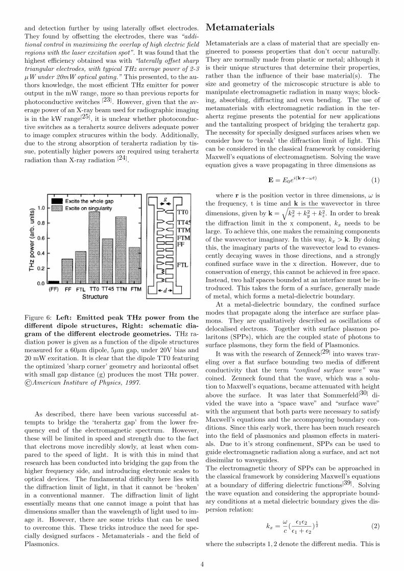
photoconductive switch[26]. Therefore, Brener focused onoptimizing the geometry of the anode to increase the elec-tric field acting on the charge carriers. The geometry wasoptimized by increasing the number of ‘sharp corners’ onthe anode, thus increasing the number of electric field sin-gularities that the charge carriers in the anode would inter-act with. It was shown that in doing this, the maximumemission of terahertz radiation was increased by almost oneorder of magnitude than at the cathode of the photoconduc-tive switch. Figure 5 shows the geometric structure of theanodes in question, and the terahertz emission from them.
Figure 5: Images of different anode geometries andthe resulting THz emission scans. Images a) and b) re-spectively show the initial ’triangular’ shaped anode and thesubsequently optimized anode with more ’sharp corners’.The emission scans (c) and d)) clearly show the enhancedTHz emission from the anode with an increased number of’sharp corners’. ©Optical Letters, 1996.
Despite the successful enhancement of the terahertzemission, the authors also observed that for a given elec-trode spacing, the THz emission became saturated, thuslimiting the efficiency of the emitter. Brener, along with Cai
and Federici[22], then went on to enhance terahertz emission
1An electric field singularity takes its nature from the fact that using Gauss’ law, one can shrink the Gaussian surface to an arbitrarilysmall size (r → 0) and still contain the charge source.
3
and detection further by using laterally offset electrodes.They found by offsetting the electrodes, there was “addi-tional control in maximizing the overlap of high electric fieldregions with the laser excitation spot”. It was found that thehighest efficiency obtained was with “laterally offset sharptriangular electrodes, with typical THz average power of 2-3µW under 20mW optical gating.” This presented, to the au-thors knowledge, the most efficient THz emitter for poweroutput in the mW range, more so than previous reports for
photoconductive switches [23]. However, given that the av-erage power of an X-ray beam used for radiographic imaging
is in the kW range[25], it is unclear whether photoconduc-tive switches as a terahertz source delivers adequate powerto image complex strucures within the body. Additionally,due to the strong absorption of terahertz radiation by tis-sue, potentially higher powers are required using terahertz
radiation than X-ray radiation [24].
Figure 6: Left: Emitted peak THz power from thedifferent dipole structures, Right: schematic dia-gram of the different electrode geometries. THz ra-diation power is given as a function of the dipole structuresmeasured for a 60µm dipole, 5µm gap, under 20V bias and20 mW excitation. It is clear that the dipole TT0 featuringthe optimized ’sharp corner’ geometry and horizontal offsetwith small gap distance (g) produces the most THz power.©American Institure of Physics, 1997.
As described, there have been various successful at-tempts to bridge the ‘terahertz gap’ from the lower fre-quency end of the electromagnetic spectrum. However,these will be limited in speed and strength due to the factthat electrons move incredibly slowly, at least when com-pared to the speed of light. It is with this in mind thatresearch has been conducted into bridging the gap from thehigher frequency side, and introducing electronic scales tooptical devices. The fundamental difficulty here lies withthe diffraction limit of light, in that it cannot be ‘broken’in a conventional manner. The diffraction limit of lightessentially means that one cannot image a point that hasdimensions smaller than the wavelength of light used to im-age it. However, there are some tricks that can be usedto overcome this. These tricks introduce the need for spe-cially designed surfaces - Metamaterials - and the field ofPlasmonics.
Metamaterials
Metamaterials are a class of material that are specially en-gineered to possess properties that don’t occur naturally.They are normally made from plastic or metal; although itis their unique structures that determine their properties,rather than the influence of their base material(s). Thesize and geometry of the microscopic structure is able tomanipulate electromagnetic radiation in many ways; block-ing, absorbing, diffracting and even bending. The use ofmetamaterials with electromagnetic radiation in the ter-ahertz regime presents the potential for new applicationsand the tantalizing prospect of bridging the terahertz gap.The necessity for specially designed surfaces arises when weconsider how to ‘break’ the diffraction limit of light. Thiscan be considered in the classical framework by consideringMaxwell’s equations of electromagnetism. Solving the waveequation gives a wave propagating in three dimensions as
E = E0ei(k·r−ωt) (1)
where r is the position vector in three dimensions, ω isthe frequency, t is time and k is the wavevector in three
dimensions, given by k =√k2x + k2y + k2z . In order to break
the diffraction limit in the x component, kx needs to belarge. To achieve this, one makes the remaining componentsof the wavevector imaginary. In this way, kx > k. By doingthis, the imaginary parts of the wavevector lead to evanes-cently decaying waves in those directions, and a stronglyconfined surface wave in the x direction. However, due toconservation of energy, this cannot be achieved in free space.Instead, two half spaces bounded at an interface must be in-troduced. This takes the form of a surface, generally madeof metal, which forms a metal-dielectric boundary.
At a metal-dielectric boundary, the confined surfacemodes that propagate along the interface are surface plas-mons. They are qualitatively described as oscillations ofdelocalised electrons. Together with surface plasmon po-laritons (SPPs), which are the coupled state of photons tosurface plasmons, they form the field of Plasmonics.
It was with the research of Zenneck[29] into waves trav-eling over a flat surface bounding two media of differentconductivity that the term “confined surface wave” wascoined. Zenneck found that the wave, which was a solu-tion to Maxwell’s equations, became attenuated with height
above the surface. It was later that Sommerfeld[30] di-vided the wave into a “space wave” and “surface wave”with the argument that both parts were necessary to satisfyMaxwell’s equations and the accompanying boundary con-ditions. Since this early work, there has been much researchinto the field of plasmonics and plasmon effects in materi-als. Due to it’s strong confinement, SPPs can be used toguide electromagnetic radiation along a surface, and act notdissimilar to waveguides.The electromagnetic theory of SPPs can be approached inthe classical framework by considering Maxwell’s equations
at a boundary of differing dielectric functions[39]. Solvingthe wave equation and considering the appropriate bound-ary conditions at a metal dielectric boundary gives the dis-persion relation:
kx =ω
c(ε1ε2ε1 + ε2
)12 (2)
where the subscripts 1, 2 denote the different media. This is
4
the dispersion relation for a surface wave propagating alonga metal-dielectric boundary.
This dispersion relation gives information on the prop-agation length L and also the energy confinement in thedielectric. The energy confinement is quantised by evanes-cent decay length of the field perpendicular to the interface:z = 1
|kx| . It is clear from equation 2 that the energy con-
finement is strongly dependent on the frequency.
Radiation into metal occurs in the transparency regime2,[28] ω > ωp. Between the bound and radiative modes, thereis a frequency gap of purely imaginary wavevector that pro-hibits propagation. For low frequency incident radiation(mid-infrared and lower), the SPP propagation constantis close to k0 (the wavevector of the propagating wave ina vacuum) and the wave extends over many wavelengthsinto the dielectric. In this regime, SPPs become Zenneck-
Sommerfeld waves [29][30]. In the opposite regime, forhigher frequency incident radiation, the SPP frequency ap-proaches the characteristic surface plasmon frequency givenby:
ωSP =ωp√
1 + ε2(3)
By assuming negligible damping, consequential limits on thewavevector, SP frequency and group velocity cause the SPPmode to become a surface plasmon. The surface plasmonis the limiting form of the SPP, as the wavevector in thedirection of propagation approaches zero. To excite an SPPwith electromagnetic radiation, the incident photons musthave the same momentum and wavevector as the SPP. Inorder to do this, a coupling medium must be introduced;normally a prism or a grating.
Ebbesen et al.[33] observed unusual optical proper-ties in submicrometer cylindrical cavities in metallic films.They found that the periodic arrays of holes displayed un-usual spectra, in that the incident and detected light werecollinear at wavelengths greater than the period of the ar-ray. This gave evidence that the incident electromagneticradiation was coupling with plasmons on the surface of the
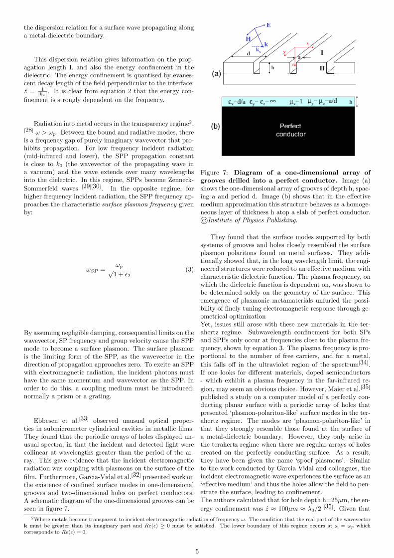
film. Furthermore, Garcia-Vidal et al.[32] presented work onthe existence of confined surface modes in one-dimensionalgrooves and two-dimensional holes on perfect conductors.A schematic diagram of the one-dimensional grooves can beseen in figure 7.
Figure 7: Diagram of a one-dimensional array ofgrooves drilled into a perfect conductor. Image (a)shows the one-dimensional array of grooves of depth h, spac-ing a and period d. Image (b) shows that in the effectivemedium approximation this structure behaves as a homoge-neous layer of thickness h atop a slab of perfect conductor.©Institute of Physics Publishing.
They found that the surface modes supported by bothsystems of grooves and holes closely resembled the surfaceplasmon polaritons found on metal surfaces. They addi-tionally showed that, in the long wavelength limit, the engi-neered structures were reduced to an effective medium withcharacteristic dielectric function. The plasma frequency, onwhich the dielectric function is dependent on, was shown tobe determined solely on the geometry of the surface. Thisemergence of plasmonic metamaterials unfurled the possi-bility of finely tuning electromagnetic response through ge-ometrical optimizationYet, issues still arose with these new materials in the ter-ahertz regime. Subwavelength confinement for both SPsand SPPs only occur at frequencies close to the plasma fre-quency, shown by equation 3. The plasma frequency is pro-portional to the number of free carriers, and for a metal,
this falls off in the ultraviolet region of the spectrum[34].If one looks for different materials, doped semiconductors- which exhibit a plasma frequency in the far-infrared re-
gion, may seem an obvious choice. However, Maier et al.[35]
published a study on a computer model of a perfectly con-ducting planar surface with a periodic array of holes thatpresented ‘plasmon-polariton-like’ surface modes in the ter-ahertz regime. The modes are ‘plasmon-polariton-like’ inthat they strongly resemble those found at the surface ofa metal-dielectric boundary. However, they only arise inthe terahertz regime when there are regular arrays of holescreated on the perfectly conducting surface. As a result,they have been given the name ‘spoof plasmons’. Similarto the work conducted by Garcia-Vidal and colleagues, theincident electromagnetic wave experiences the surface as an‘effective medium’ and thus the holes allow the field to pen-etrate the surface, leading to confinement.The authors calculated that for hole depth h=25µm, the en-
ergy confinement was z ≈ 100µm ≈ λ0/2[35]. Given that
2Where metals become transparent to incident electromagnetic radiation of frequency ω. The condition that the real part of the wavevectork must be greater than its imaginary part and Re(ε) ≥ 0 must be satisfied. The lower boundary of this regime occurs at ω = ωp whichcorresponds to Re(ε) = 0.
5
they found the maximum energy confinement as h→∞ asz ≈ 80µm ≈ 0.38λ0, the fact that a hole depth of 25µm,yields a vertical sub-wavelength confinement close to thecomputed maximum is extremely promising. It presents,due to current microfrabrication and manufacturing tech-nologies, an incredibly feasible way of producing surfacesthat can hold well-defined surface modes for the purposesof waveguiding and surface sensing.This work was further extended to three dimensions on peri-
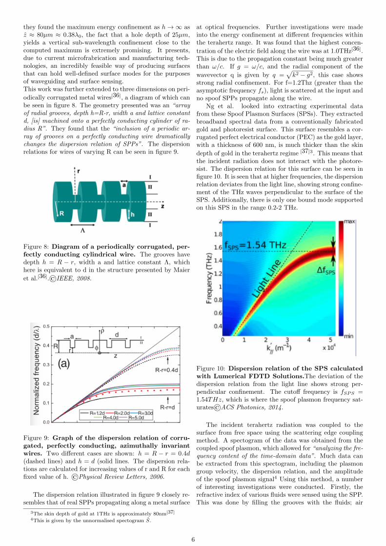
odically corrugated metal wires[36], a diagram of which canbe seen in figure 8. The geometry presented was an “arrayof radial grooves, depth h=R-r, width a and lattice constantd, [is] machined onto a perfectly conducting cylinder of ra-dius R”. They found that the “inclusion of a periodic ar-ray of grooves on a perfectly conducting wire dramaticallychanges the dispersion relation of SPPs”. The dispersionrelations for wires of varying R can be seen in figure 9.
Figure 8: Diagram of a periodically corrugated, per-fectly conducting cylindrical wire. The grooves havedepth h = R − r, width a and lattice constant Λ, whichhere is equivalent to d in the structure presented by Maier
et al.[36].©IEEE, 2008.
Figure 9: Graph of the dispersion relation of corru-gated, perfectly conducting, azimuthally invariantwires. Two different cases are shown: h = R − r = 0.4d(dashed lines) and h = d (solid lines. The dispersion rela-tions are calculated for increasing values of r and R for eachfixed value of h. ©Physical Review Letters, 2006.
The dispersion relation illustrated in figure 9 closely re-sembles that of real SPPs propagating along a metal surface
at optical frequencies. Further investigations were madeinto the energy confinement at different frequencies withinthe terahertz range. It was found that the highest concen-
tration of the electric field along the wire was at 1.0THz[36].This is due to the propagation constant being much greaterthan ω/c. If g = ω/c, and the radial component of the
wavevector q is given by q =√k2 − g2, this case shows
strong radial confinement. For f=1.2Thz (greater than theasymptotic frequency fs), light is scattered at the input andno spoof SPPs propagate along the wire.
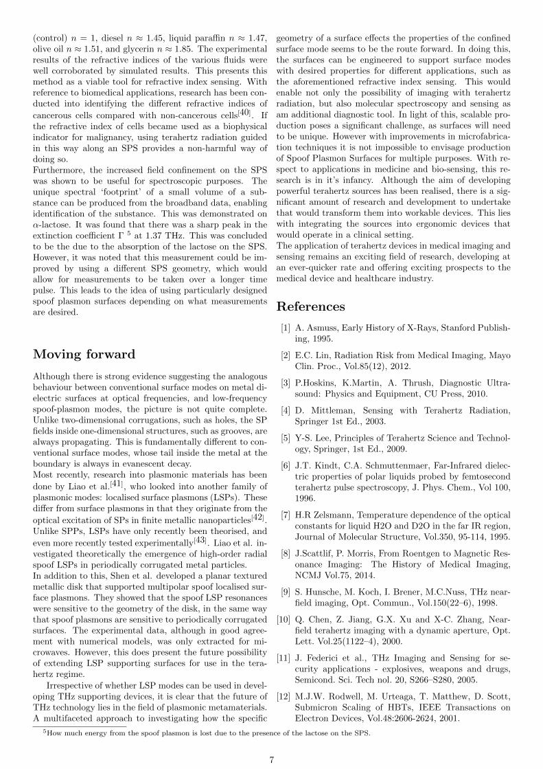
Ng et al. looked into extracting experimental datafrom these Spoof Plasmon Surfaces (SPSs). They extractedbroadband spectral data from a conventionally fabricatedgold and photoresist surface. This surface resembles a cor-rugated perfect electrical conductor (PEC) as the gold layer,with a thickness of 600 nm, is much thicker than the skin
depth of gold in the terahertz regime [37]3. This means thatthe incident radiation does not interact with the photore-sist. The dispersion relation for this surface can be seen infigure 10. It is seen that at higher frequencies, the dispersionrelation deviates from the light line, showing strong confine-ment of the THz waves perpendicular to the surface of theSPS. Additionally, there is only one bound mode supportedon this SPS in the range 0.2-2 THz.
Figure 10: Dispersion relation of the SPS calculatedwith Lumerical FDTD Solutions.The deviation of thedispersion relation from the light line shows strong per-pendicular confinement. The cutoff frequency is fSPS =1.54THz, which is where the spoof plasmon frequency sat-urates©ACS Photonics, 2014.
The incident terahertz radiation was coupled to thesurface from free space using the scattering edge couplingmethod. A spectogram of the data was obtained from thecoupled spoof plasmon, which allowed for “analyzing the fre-quency content of the time-domain data”. Much data canbe extracted from this spectogram, including the plasmongroup velocity, the dispersion relation, and the amplitudeof the spoof plasmon signal4 Using this method, a numberof interesting investigations were conducted. Firstly, therefractive index of various fluids were sensed using the SPP.This was done by filling the grooves with the fluids; air
3The skin depth of gold at 1THz is approximately 80nm[37]
4This is given by the unnormalised spectogram S.
6
(control) n = 1, diesel n ≈ 1.45, liquid paraffin n ≈ 1.47,olive oil n ≈ 1.51, and glycerin n ≈ 1.85. The experimentalresults of the refractive indices of the various fluids werewell corroborated by simulated results. This presents thismethod as a viable tool for refractive index sensing. Withreference to biomedical applications, research has been con-ducted into identifying the different refractive indices of
cancerous cells compared with non-cancerous cells[40]. Ifthe refractive index of cells became used as a biophysicalindicator for malignancy, using terahertz radiation guidedin this way along an SPS provides a non-harmful way ofdoing so.Furthermore, the increased field confinement on the SPSwas shown to be useful for spectroscopic purposes. Theunique spectral ‘footprint’ of a small volume of a sub-stance can be produced from the broadband data, enablingidentification of the substance. This was demonstrated onα-lactose. It was found that there was a sharp peak in theextinction coefficient Γ 5 at 1.37 THz. This was concludedto be the due to the absorption of the lactose on the SPS.However, it was noted that this measurement could be im-proved by using a different SPS geometry, which wouldallow for measurements to be taken over a longer timepulse. This leads to the idea of using particularly designedspoof plasmon surfaces depending on what measurementsare desired.
Moving forward
Although there is strong evidence suggesting the analogousbehaviour between conventional surface modes on metal di-electric surfaces at optical frequencies, and low-frequencyspoof-plasmon modes, the picture is not quite complete.Unlike two-dimensional corrugations, such as holes, the SPfields inside one-dimensional structures, such as grooves, arealways propagating. This is fundamentally different to con-ventional surface modes, whose tail inside the metal at theboundary is always in evanescent decay.Most recently, research into plasmonic materials has been
done by Liao et al.[41], who looked into another family ofplasmonic modes: localised surface plasmons (LSPs). Thesediffer from surface plasmons in that they originate from the
optical excitation of SPs in finite metallic nanoparticles[42].Unlike SPPs, LSPs have only recently been theorised, and
even more recently tested experimentally[43]. Liao et al. in-vestigated theoretically the emergence of high-order radialspoof LSPs in periodically corrugated metal particles.In addition to this, Shen et al. developed a planar texturedmetallic disk that supported multipolar spoof localised sur-face plasmons. They showed that the spoof LSP resonanceswere sensitive to the geometry of the disk, in the same waythat spoof plasmons are sensitive to periodically corrugatedsurfaces. The experimental data, although in good agree-ment with numerical models, was only extracted for mi-crowaves. However, this does present the future possibilityof extending LSP supporting surfaces for use in the tera-hertz regime.
Irrespective of whether LSP modes can be used in devel-oping THz supporting devices, it is clear that the future ofTHz technology lies in the field of plasmonic metamaterials.A multifaceted approach to investigating how the specific
geometry of a surface effects the properties of the confinedsurface mode seems to be the route forward. In doing this,the surfaces can be engineered to support surface modeswith desired properties for different applications, such asthe aforementioned refractive index sensing. This wouldenable not only the possibility of imaging with terahertzradiation, but also molecular spectroscopy and sensing asam additional diagnostic tool. In light of this, scalable pro-duction poses a significant challenge, as surfaces will needto be unique. However with improvements in microfabrica-tion techniques it is not impossible to envisage productionof Spoof Plasmon Surfaces for multiple purposes. With re-spect to applications in medicine and bio-sensing, this re-search is in it’s infancy. Although the aim of developingpowerful terahertz sources has been realised, there is a sig-nificant amount of research and development to undertakethat would transform them into workable devices. This lieswith integrating the sources into ergonomic devices thatwould operate in a clinical setting.The application of terahertz devices in medical imaging andsensing remains an exciting field of research, developing atan ever-quicker rate and offering exciting prospects to themedical device and healthcare industry.
References
[1] A. Asmuss, Early History of X-Rays, Stanford Publish-ing, 1995.
[2] E.C. Lin, Radiation Risk from Medical Imaging, MayoClin. Proc., Vol.85(12), 2012.
[3] P.Hoskins, K.Martin, A. Thrush, Diagnostic Ultra-sound: Physics and Equipment, CU Press, 2010.
[4] D. Mittleman, Sensing with Terahertz Radiation,Springer 1st Ed., 2003.
[5] Y-S. Lee, Principles of Terahertz Science and Technol-ogy, Springer, 1st Ed., 2009.
[6] J.T. Kindt, C.A. Schmuttenmaer, Far-Infrared dielec-tric properties of polar liquids probed by femtosecondterahertz pulse spectroscopy, J. Phys. Chem., Vol 100,1996.
[7] H.R Zelsmann, Temperature dependence of the opticalconstants for liquid H2O and D2O in the far IR region,Journal of Molecular Structure, Vol.350, 95-114, 1995.
[8] J.Scattlif, P. Morris, From Roentgen to Magnetic Res-onance Imaging: The History of Medical Imaging,NCMJ Vol.75, 2014.
[9] S. Hunsche, M. Koch, I. Brener, M.C.Nuss, THz near-field imaging, Opt. Commun., Vol.150(22–6), 1998.
[10] Q. Chen, Z. Jiang, G.X. Xu and X-C. Zhang, Near-field terahertz imaging with a dynamic aperture, Opt.Lett. Vol.25(1122–4), 2000.
[11] J. Federici et al., THz Imaging and Sensing for se-curity applications - explosives, weapons and drugs,Semicond. Sci. Tech nol. 20, S266–S280, 2005.
[12] M.J.W. Rodwell, M. Urteaga, T. Matthew, D. Scott,Submicron Scaling of HBTs, IEEE Transactions onElectron Devices, Vol.48:2606-2624, 2001.
5How much energy from the spoof plasmon is lost due to the presence of the lactose on the SPS.
7
[13] D.H. Auston, Picosecond optoelectronic switching andgating in silicon, Applied Physics Letters, Vol.26(3),1975.
[14] U.Keller, W.H. Knox, G.W. Hooft, Ultrafast solid-state mode-locked laser using resonant nonlinearities,IEEE Journal of Quantum Electronics, Vol.208(10),1992.
[15] B.B Hu, M.C. Nuss, Imaging with terahertz waves, Op-tical Letters, Vol.20(16), 1995.
[16] D.M. Mittleman, R.H. Jacobsen, M.C.Nuss, T-RayImaging, IEEE Journal of selected topics in QuantumElectronics, Vol.2(3), 1996.
[17] V.P. Wallace, D.A. Arnone, R.M.Woodward, R.J. Pye,Biomedical Applications of terahertz pulse imaging,IEEE, 2002.
[18] S. Mangles, Medical Imaging: X-Ray and Ultrasound(lecture notes), 2016.
[19] D. Kopf, K.J. Weingarten, L.R. Brovelli, M.Kamp,U. Keller, Diode-pumped 100-fs passively mode-lockedCr:LiSAF laser with an antiresonant Fabry-Perot sat-urable absorber, Opt. Lett., Vol.19, 1994.
[20] N.H. Rizvi, P.M.W. French, J.R. Taylor, 50-fs pulsegeneration from a self-starting CW passively mode-locked Cr:LiSrAlF laser, Opt. Lett. Vol.17, 1992.
[21] I. Brener, D. Dykaar, A. Frommer, L.N. Pfeiffer, J.Lopota, J. Wynn, K. West, M.C. Nuss, Terahertz emis-sion from electric field singularities in biased semicon-ductors, Opt. Lett., Vol.21(23), 1996.
[22] Y. Cai, I. Brener, J. Lopata, J.Wynn, L. Pfeiffer, J.Federici, Design and performance of singular electricfield terahertz photoconducting antennas, Appl. Phys.Lett., Vol.71(15), 1997.
[23] M.V Exter, D. Grischowsky, Characterisation of Op-toelectronic Terahertz Beam System, IEEE Trans. Mi-crowave Techn., Vol.38, 1990.
[24] S.W. Smye, J.M. Chamber, A.J. Fitzgerald, E. Berry,The interaction between Terahertz radiation and bio-logical tissue, Phys. Med. Biol., Vol.46, 2001.
[25] J.T Bushberg, J.A. Seibert, E.M Leidholdt Jr., J.M.Boone, The Essential Physics of Medical Imaging, Lip-pincott, Williams & Wilkins Pub., 2nd Ed., 2002.
[26] D. Krockel, D. Grischkowsky, M.B Ketchen, Sub-picosecond electrical pulse generation using photocon-ductive switches with long carrier lifetimes, Appl. Phys.Lett. Vol.54(11), 1989.
[27] T. Ouchi, K. Kajiki, T. Koizumi, T. Ituski, Y. Koyama,R. Sekiguchi, O. Kuboto, K. Kawase, Terahertz Imag-ing System for Medical Applications and Related HighEfficiency Terahertz Devices, J. Infrared Milli TerahzWaves, Vol.35(118-130), 2014.
[28] E-P. Li, H-S. Chu, Plasmonic Nanoelectronics andSensing, Camb. Uni. Press, 1st ed., 2014.
[29] J. Zenneck, About the propagation of plane electro-magnetic waves along a planar conductor area andits relation to wireless telegraphy, Ann. Physik, Vol.328(10), 1907.
[30] A. Sommerfeld, About the propagation of waves in theWireless Telegraphy, Ann. Physik, Vol.333(4), 1909.
[31] J.R. Wait, Excitation of Surface Waves on Conducting,Stratified, Dielectric-Clad, and Corrugated Surfaces, J.Res. Nat. Bur. Stand., Vol.59(6), 1957.
[32] F.J. Garcia-Vidal, L Martin-Moreno, J.B. Pendry, Sur-faces with holes in them: new plasmonic metamateri-als, J. Opt. A: Pure Appl. Opt., Vol 7, 2005.
[33] T.W. Ebbesen, H.J. Lezec, H.F. Ghaemi, T.Thio, P.A.Wolff, Extraordinary optical transmission through sub-wavelength hole arrays, Nature, Vol. 391, 1998.
[34] F.J. Himpsel, plasmonics, Physics Dept., University ofWisconsin Madison, 2014.
[35] S.A. Maier, S.R. Andrews, Terahertz pulse propagationusing plasmon-polariton-like surface modes on struc-tured conductive surfaces, App. Phys. Lett. Vol.88,2006.
[36] S.A. Maier, S.R. Andrews, L. Martin-Moreno, F.JGarcia-Vidal, Terahertz Surface Plasmon-PolaritonPropagation and Focusing on Periodically CorrugatedMetal Wires, Phys. Rev. Lett. Vol.97, 2006.
[37] H.R. Park, S.M. Koo, O.K. Suwal, Y.M. Park, J.S.Kyoung, M.A. Seo, S.S. Choi, N.K. Park, D.S. Kim,K.J. Ahn, Resonance behaviour of single ultrathin slotantennas on finite dielectric substrates in terahertzregime, App. Phys. Lett., Vol.96, 2010.
[38] M. Mansuripur, Classical Optics and it’s Applications,Cambridge University Press, Ed.2., 2011.
[39] M.G Cottam, D.R. Tilley, Introduction to Surface andSuperlattice Excitations, Inst. of Phys. Pub., Ed.2,1989
[40] W.J. Choi, D.I. Jeon, S-G. Ahn, J-H. Yoon, S. Kim,B.H. Lee, Full-field optical coherence microscopy foridentifying live cancer cells by quantitative measure-ments of refractive index distribution, Optics Express,Vol. 18(22), 2010.
[41] Z. Liao, Y. Lou, A.I. Fernandez-Dominguez, X. Shen,S.A. Maier, T.J. Cui, High-order localized spoof sur-face plasmon resonances and experimental verifica-tions, Scientific Reports, Vol.5, 2015.
[42] U. Kreibig, & M. Vollmer, Optical properties of metalclusters, Springer-Verlag, 1995.
[43] X. Shen, T.J. Cui, Ultrathin plasmonic metamaterialfor spoof localized surface plasmons, Laser & Photonicsreview, Vol 8.(1), 2014.
8