nanophotonics: solar and thermal applications -...
TRANSCRIPT
Nanophotonics: solar and thermal applications
Shanhui Fan
Ginzton Laboratory and Department of Electrical Engineering
Stanford University
http://www.stanford.edu/~shanhui
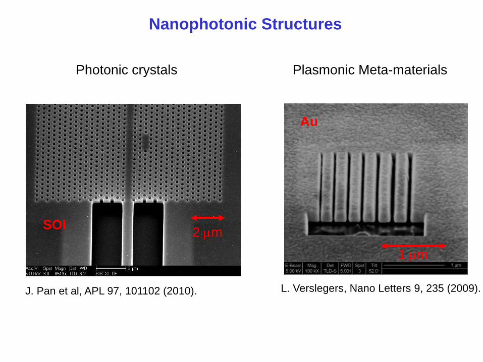
Nanophotonic Structures
Photonic crystals Plasmonic Meta-materials
1 m
Au
2 m SOI
J. Pan et al, APL 97, 101102 (2010). L. Verslegers, Nano Letters 9, 235 (2009).

Photon as an important heat carrier
On earth From the sun
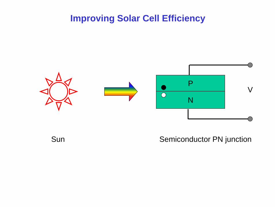
Improving Solar Cell Efficiency
P
N
V
Sun Semiconductor PN junction
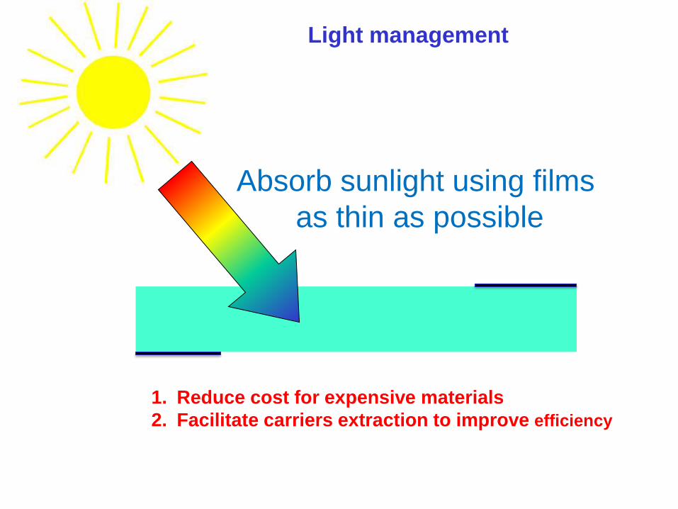
1. Reduce cost for expensive materials
2. Facilitate carriers extraction to improve efficiency
Absorb sunlight using films
as thin as possible
Light management
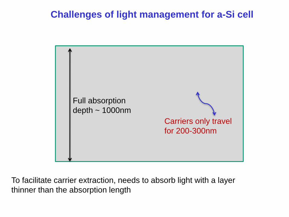
Full absorption
depth ~ 1000nm
Carriers only travel
for 200-300nm
To facilitate carrier extraction, needs to absorb light with a layer
thinner than the absorption length
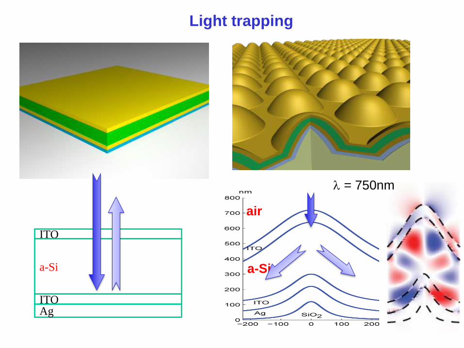
Challenges of light management for a-Si cell
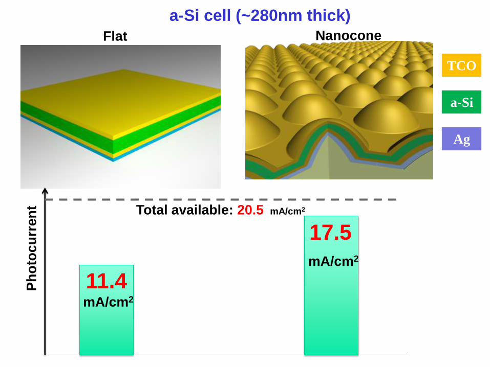
TCO
a-Si
Ag
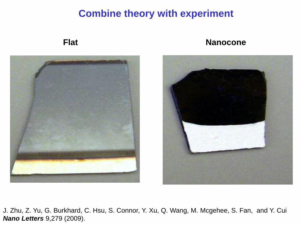
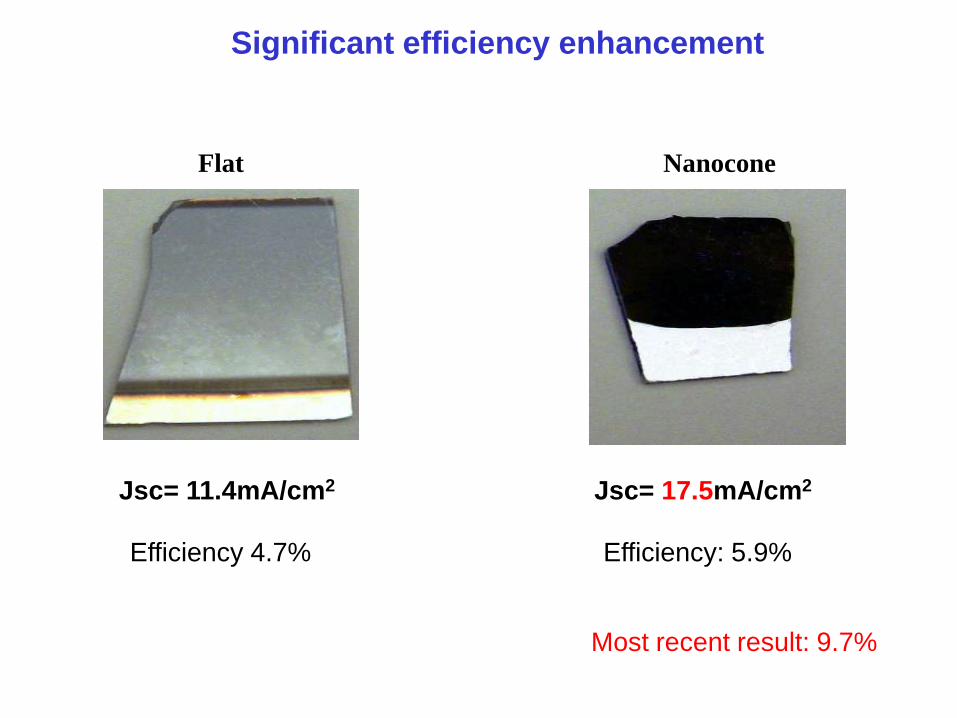
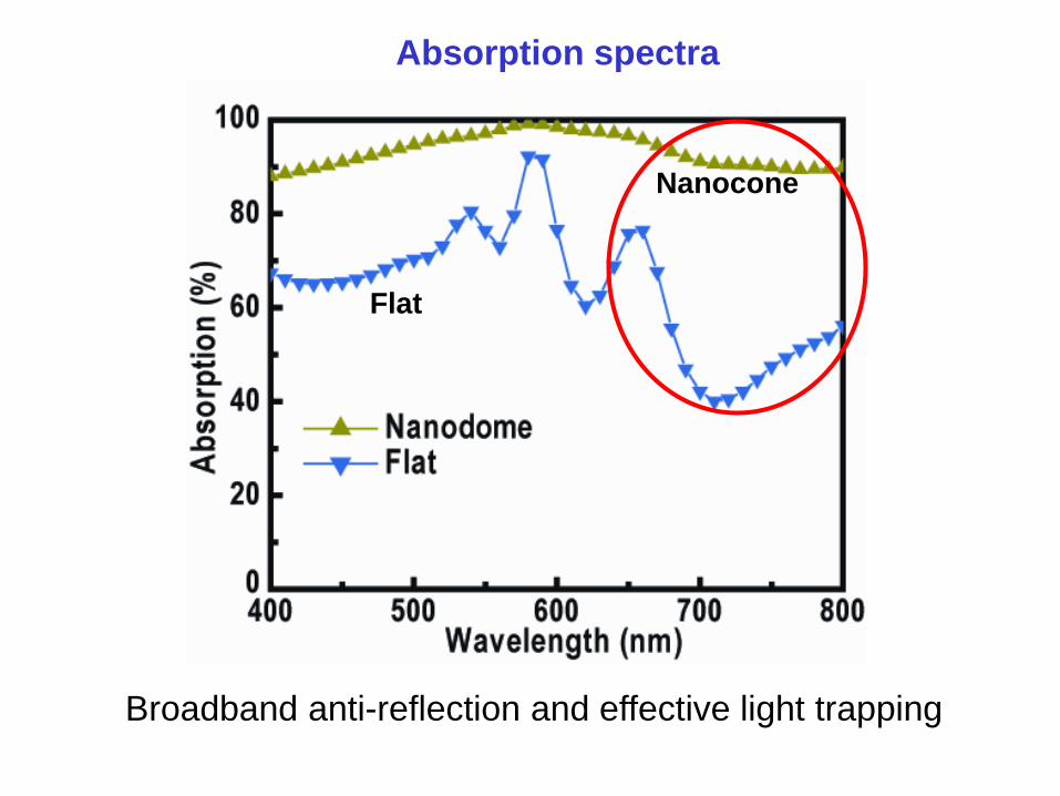
Flat Nanocone
11.4 mA/cm2
17.5
mA/cm2
Ph
oto
cu
rre
nt Total available: 20.5 mA/cm2
a-Si cell (~280nm thick)
Flat
Nanocone
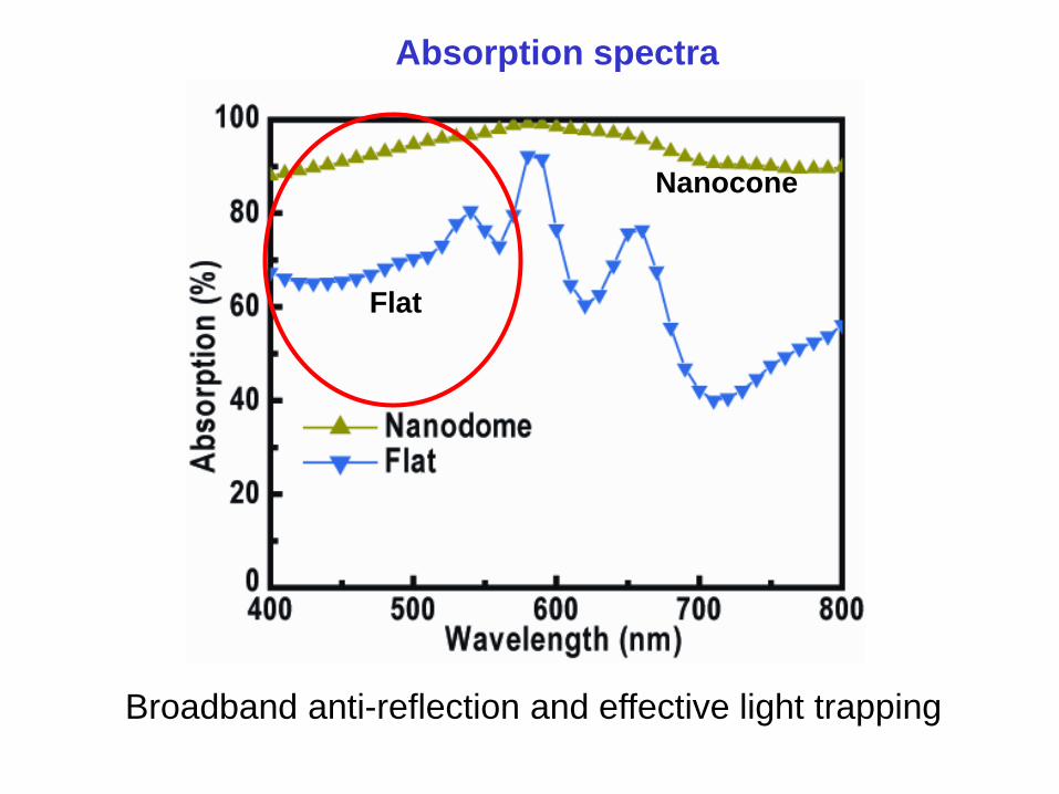
Broadband anti-reflection and effective light trapping
Absorption spectra
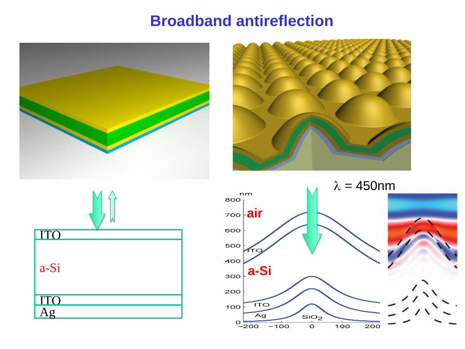
ITO
a-Si
ITO Ag
air
a-Si
Broadband antireflection
l = 450nm

Flat
Nanocone
Broadband anti-reflection and effective light trapping
Absorption spectra
ITO
a-Si
ITO Ag
air
a-Si
Light trapping
l = 750nm
Flat Nanocone
J. Zhu, Z. Yu, G. Burkhard, C. Hsu, S. Connor, Y. Xu, Q. Wang, M. Mcgehee, S. Fan, and Y. Cui
Nano Letters 9,279 (2009).
Combine theory with experiment
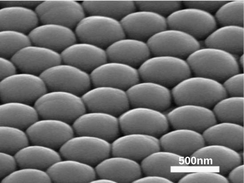
500nm
Flat Nanocone
Jsc= 11.4mA/cm2 Jsc= 17.5mA/cm2
Efficiency 4.7% Efficiency: 5.9%
Most recent result: 9.7%
Significant efficiency enhancement
Flat
Nanocone
Broadband anti-reflection and effective light trapping
Absorption spectra
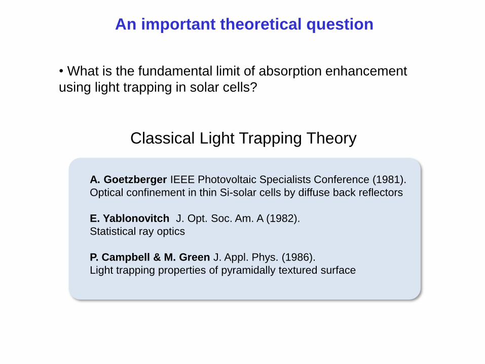
An important theoretical question
• What is the fundamental limit of absorption enhancement
using light trapping in solar cells?
A. Goetzberger IEEE Photovoltaic Specialists Conference (1981).
Optical confinement in thin Si-solar cells by diffuse back reflectors
E. Yablonovitch J. Opt. Soc. Am. A (1982).
Statistical ray optics
P. Campbell & M. Green J. Appl. Phys. (1986).
Light trapping properties of pyramidally textured surface
Classical Light Trapping Theory
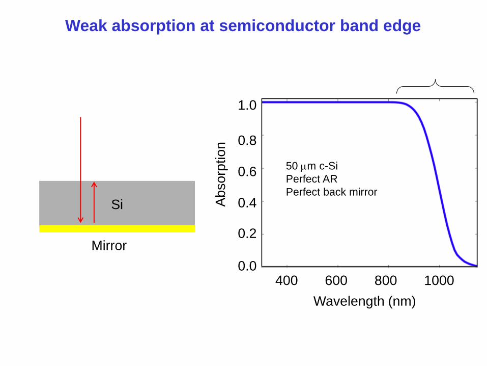
50 m c-Si
Perfect AR
Perfect back mirror
0.2
0.4
0.6
0.8
1.0
0.0 400 600 800 1000
Wavelength (nm)
Ab
so
rptio
n
Weak absorption at semiconductor band edge
Si
Mirror
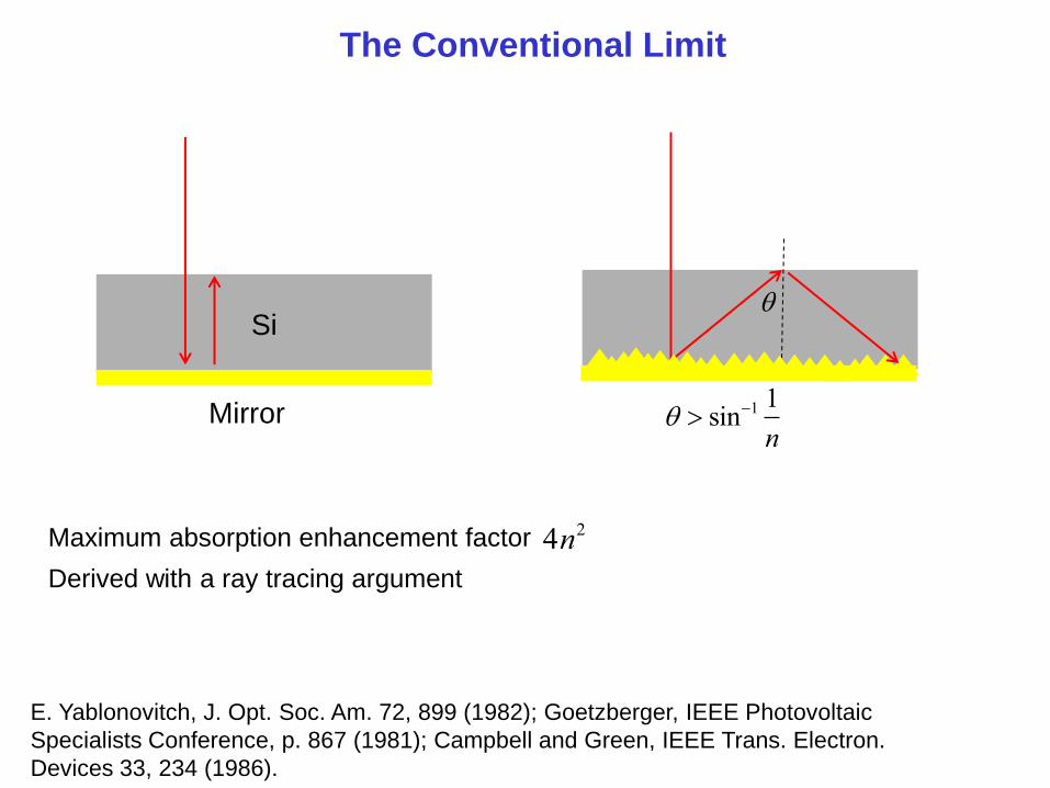
The Conventional Limit
Si
Mirror sin1 1
n
Maximum absorption enhancement factor
Derived with a ray tracing argument
4n2
E. Yablonovitch, J. Opt. Soc. Am. 72, 899 (1982); Goetzberger, IEEE Photovoltaic
Specialists Conference, p. 867 (1981); Campbell and Green, IEEE Trans. Electron.
Devices 33, 234 (1986).
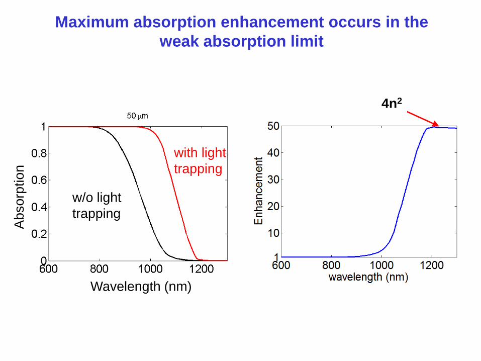
Maximum absorption enhancement occurs in the
weak absorption limit
w/o light
trapping
with light
trapping
Wavelength (nm)
Ab
so
rptio
n
4n2
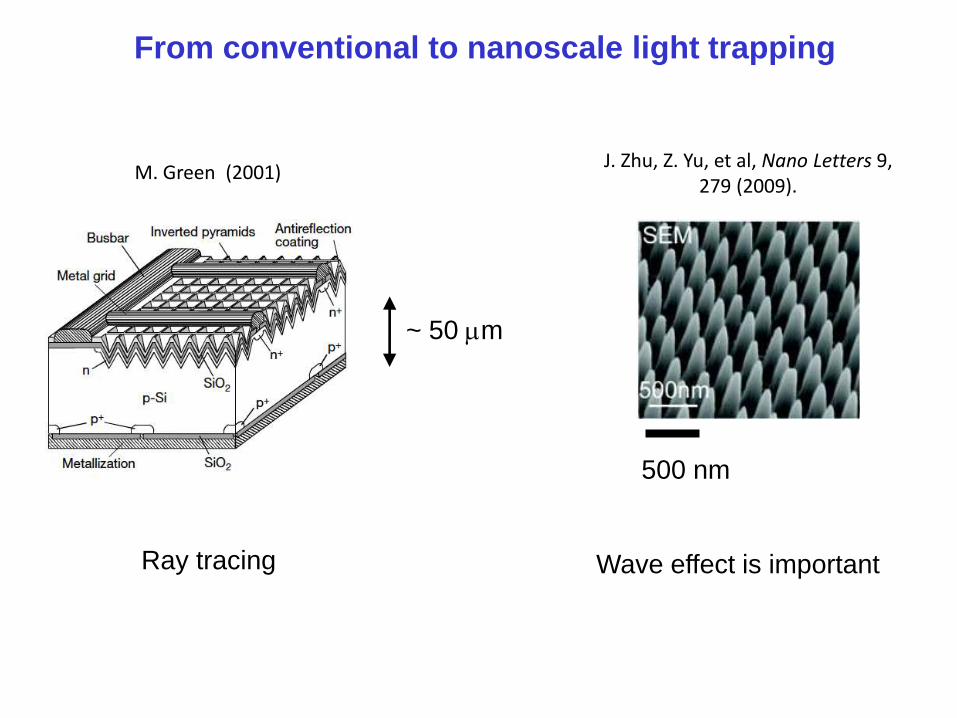
Nanocone
J. Zhu, Z. Yu, et al, Nano Letters 9, 279 (2009).
From conventional to nanoscale light trapping
~ 50 m
500 nm
Ray tracing Wave effect is important
M. Green (2001)
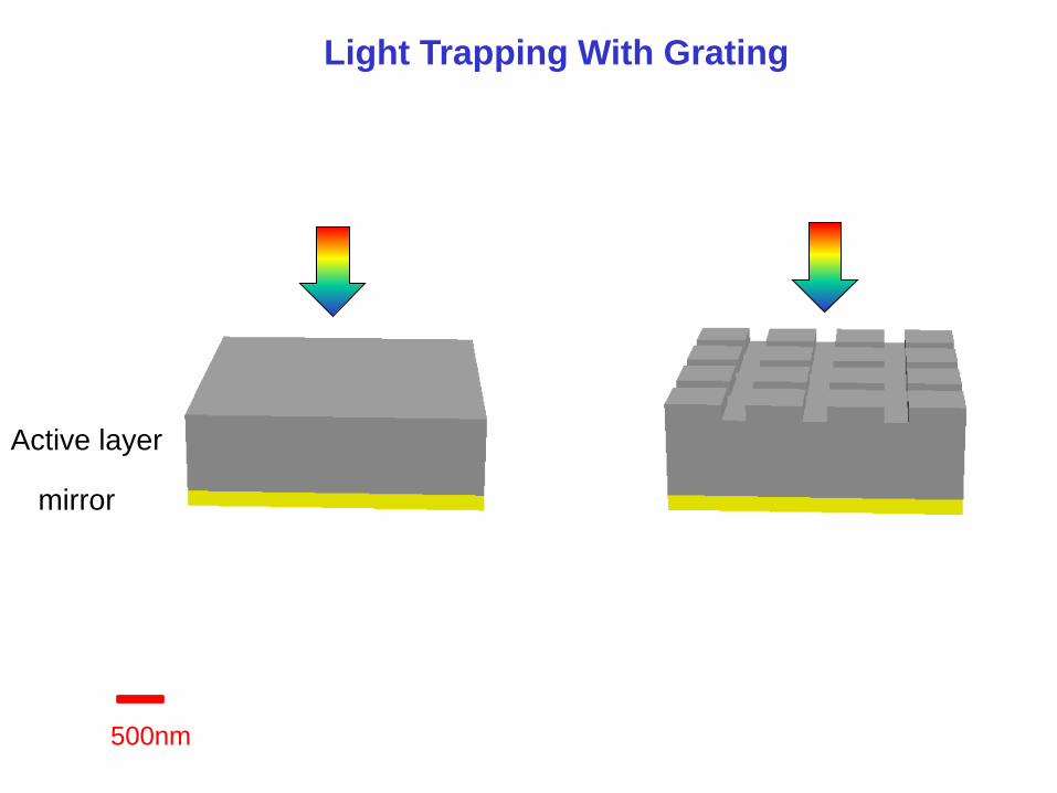
Light Trapping With Grating
mirror
Active layer
500nm
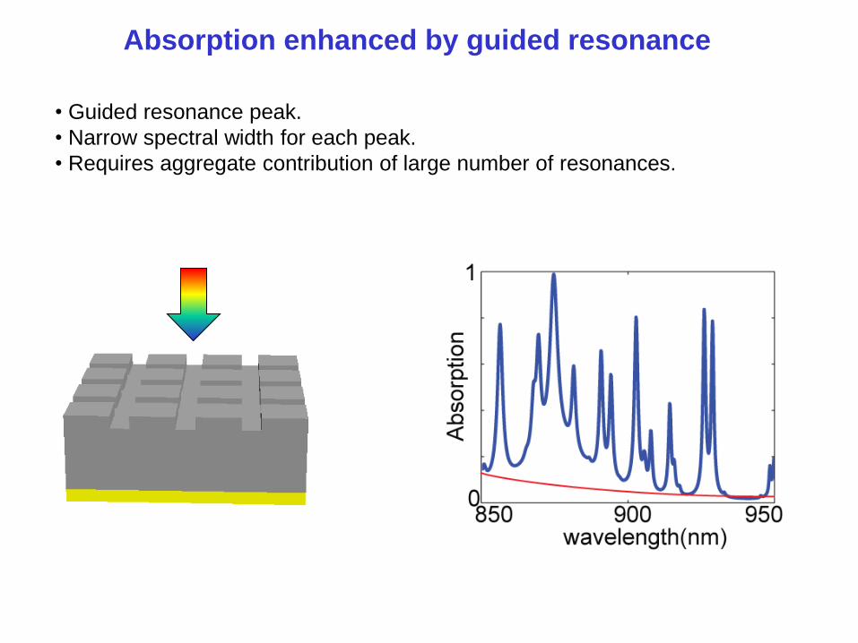
Absorption enhanced by guided resonance
• Guided resonance peak.
• Narrow spectral width for each peak.
• Requires aggregate contribution of large number of resonances.
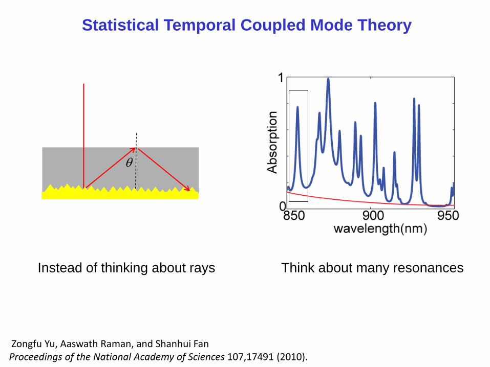
Statistical Temporal Coupled Mode Theory
Instead of thinking about rays Think about many resonances
Zongfu Yu, Aaswath Raman, and Shanhui Fan Proceedings of the National Academy of Sciences 107,17491 (2010).
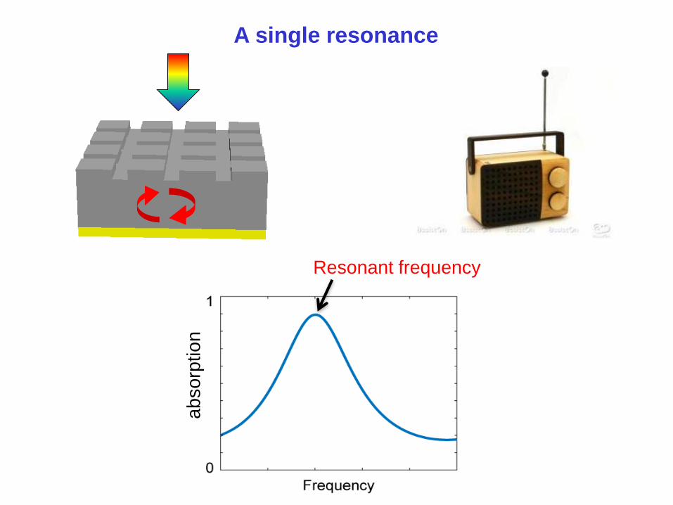
A single resonance
Resonant frequency
ab
so
rptio
n
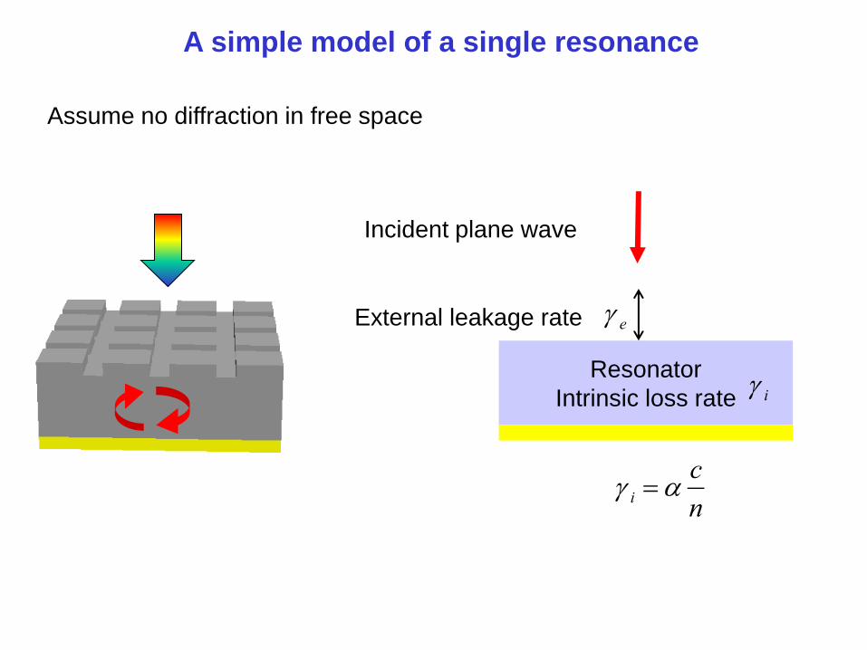
Resonator
Intrinsic loss rate
External leakage rate
Incident plane wave
A simple model of a single resonance
i c
n
Assume no diffraction in free space
i
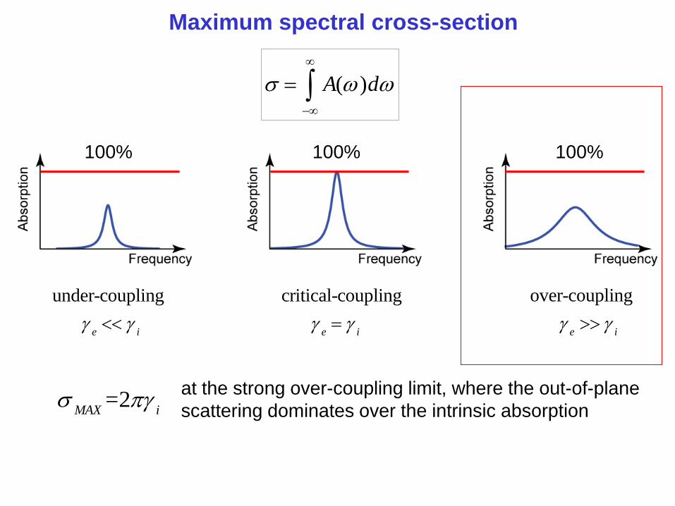
e
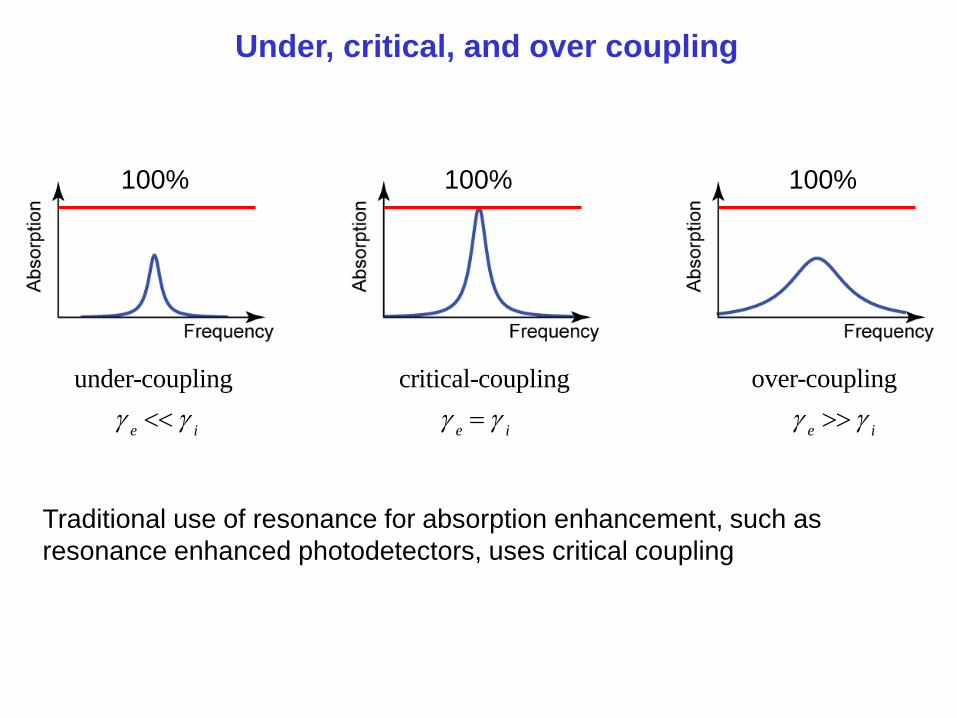
under-coupling
e
i
critical-coupling
e
i
over-coupling
e
i
Under, critical, and over coupling
100% 100% 100%
Traditional use of resonance for absorption enhancement, such as
resonance enhanced photodetectors, uses critical coupling
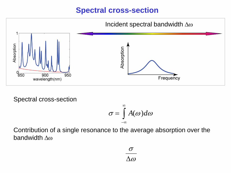
Spectral cross-section
Spectral cross-section
Contribution of a single resonance to the average absorption over the
bandwidth
A( )d
Incident spectral bandwidth
100% 100% 100%
Maximum spectral cross-section
MAX=2
i
A( )d
at the strong over-coupling limit, where the out-of-plane
scattering dominates over the intrinsic absorption
under-coupling
e
i
critical-coupling
e
i
over-coupling
e
i
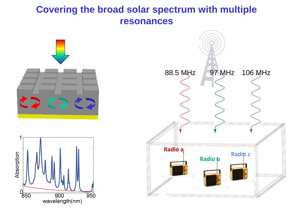
Radio a
Radio b Radio c
88.5 MHz 97 MHz 106 MHz
Covering the broad solar spectrum with multiple
resonances
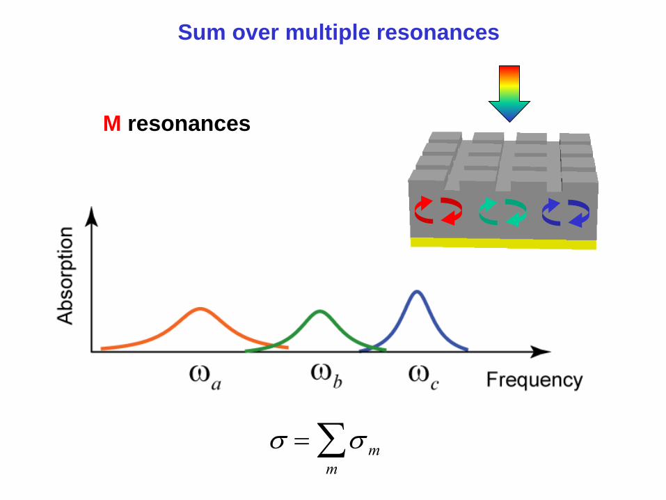
Sum over multiple resonances
M resonances
m
m
M resonances
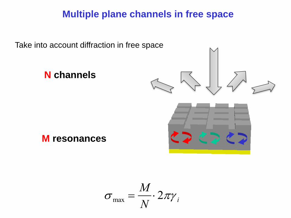
N channels
Multiple plane channels in free space
max M
N2 i
Take into account diffraction in free space
=
M
N2
i
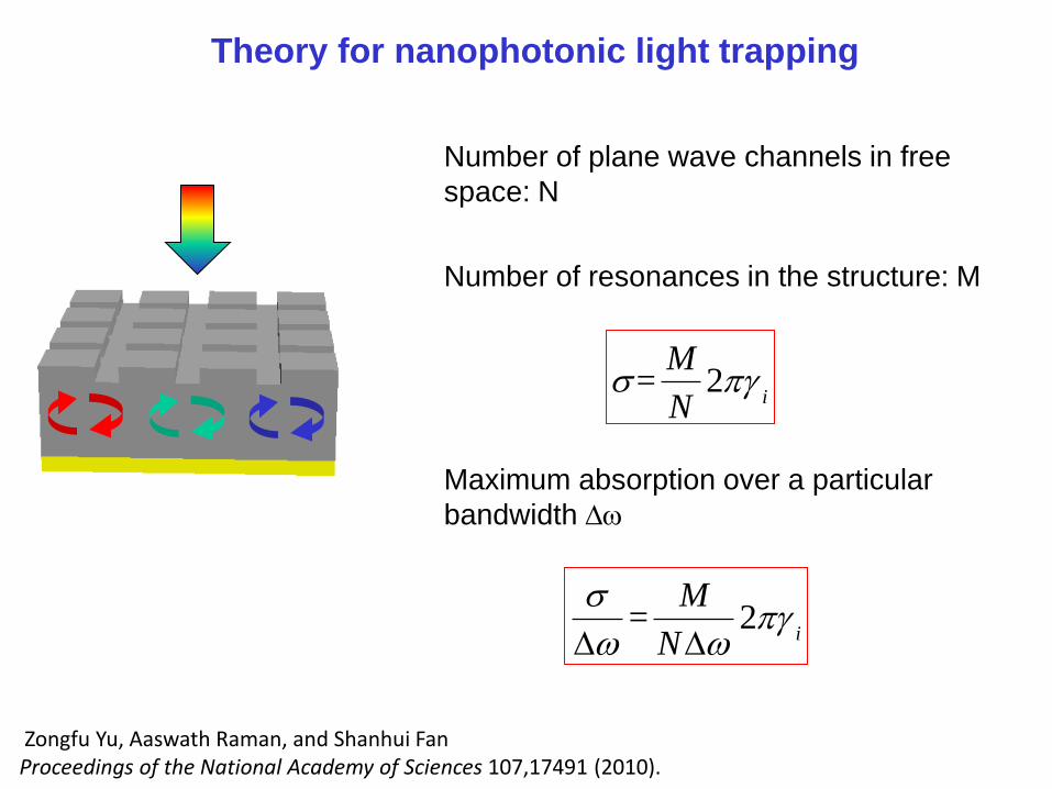
Theory for nanophotonic light trapping
Number of resonances in the structure: M
Number of plane wave channels in free
space: N
Maximum absorption over a particular
bandwidth
=
M
N2
i
Zongfu Yu, Aaswath Raman, and Shanhui Fan Proceedings of the National Academy of Sciences 107,17491 (2010).
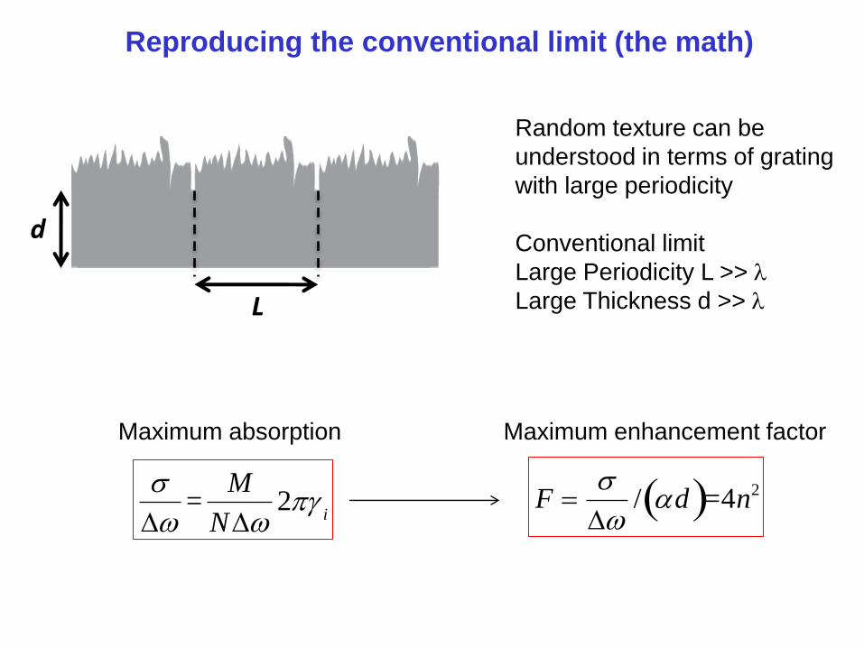
Reproducing the conventional limit (the math)
Random texture can be
understood in terms of grating
with large periodicity
Conventional limit
Large Periodicity L >> l
Large Thickness d >> l
=
M
N2
i F
/ d =4n2
L
d
Maximum absorption Maximum enhancement factor
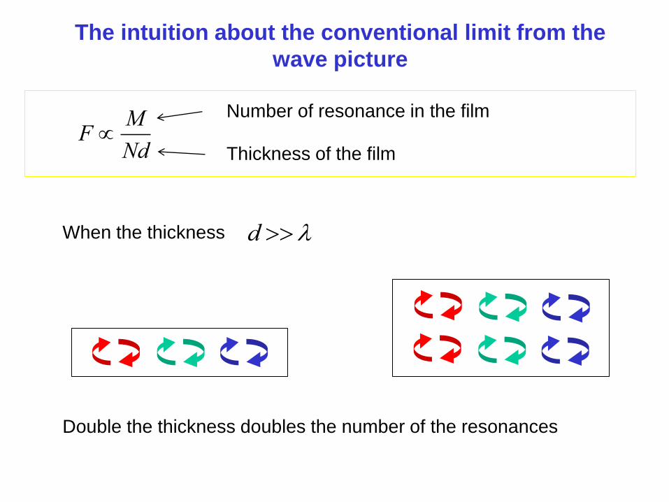
The intuition about the conventional limit from the
wave picture
F M
Nd
Number of resonance in the film
Thickness of the film
When the thickness
d l
Double the thickness doubles the number of the resonances
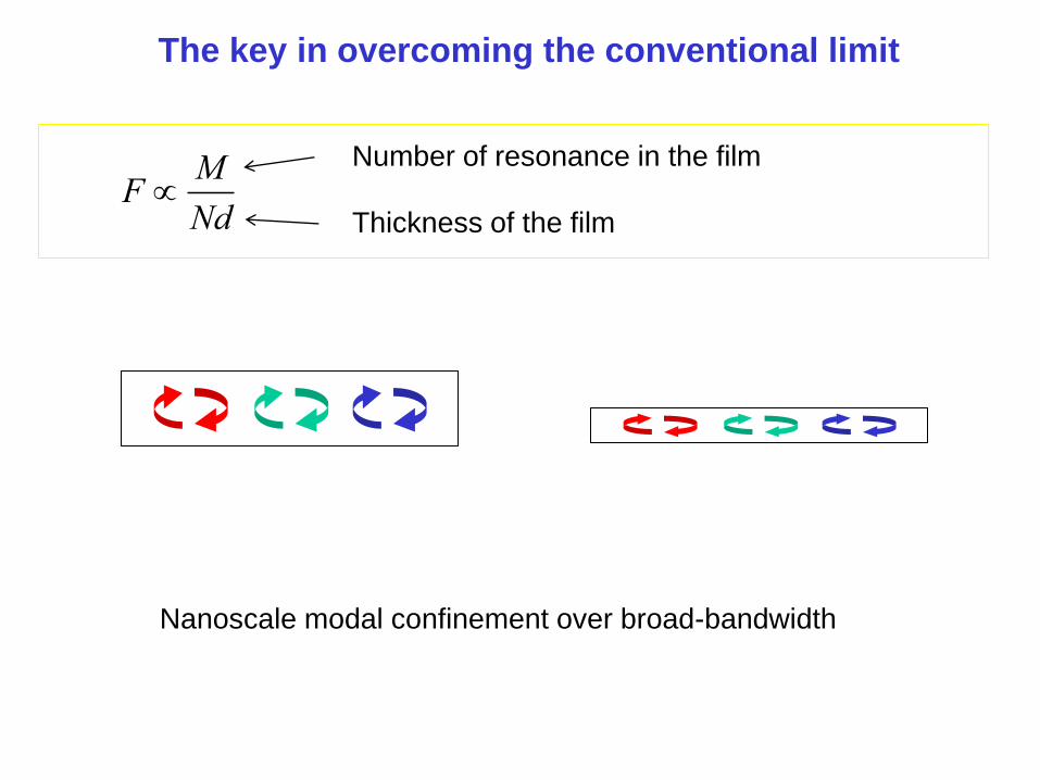
The key in overcoming the conventional limit
F M
Nd
Number of resonance in the film
Thickness of the film
Nanoscale modal confinement over broad-bandwidth
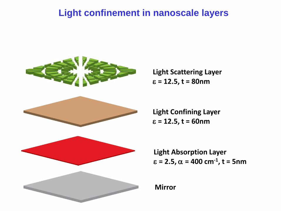
Light Scattering Layer e = 12.5, t = 80nm
Light Confining Layer e = 12.5, t = 60nm
Light Absorption Layer e = 2.5, = 400 cm-1, t = 5nm
Mirror
Light confinement in nanoscale layers
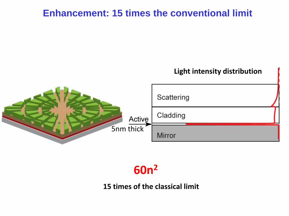
60n2
Light intensity distribution
5nm thick
15 times of the classical limit
Enhancement: 15 times the conventional limit
Zongfu Yu, Aaswath Raman, and Shanhui Fan Proceedings of the National Academy of Sciences 107,17491 (2010).
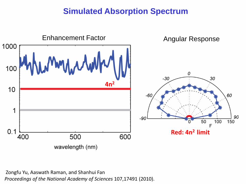
Red: 4n2 limit
Simulated Absorption Spectrum
4n2
Enhancement Factor Angular Response

Statistical Temporal Coupled Mode Theory
Instead of thinking about rays Think about many resonances
Zongfu Yu, Aaswath Raman, and Shanhui Fan Proceedings of the National Academy of Sciences 107,17491 (2010).
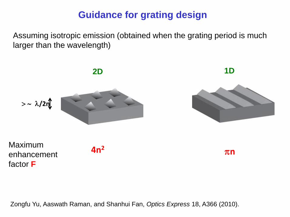
Guidance for grating design
Zongfu Yu, Aaswath Raman, and Shanhui Fan, Optics Express 18, A366 (2010).
2D 1D
Assuming isotropic emission (obtained when the grating period is much
larger than the wavelength)
4n2 n
~ l/2n
Maximum
enhancement
factor F
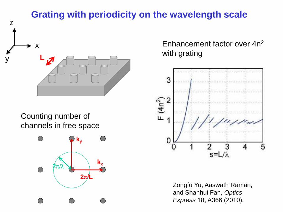
Grating with periodicity on the wavelength scale
L
x
y
z
Counting number of
channels in free space
2/L
kx
ky
2/l
Enhancement factor over 4n2
with grating
Zongfu Yu, Aaswath Raman,
and Shanhui Fan, Optics
Express 18, A366 (2010).
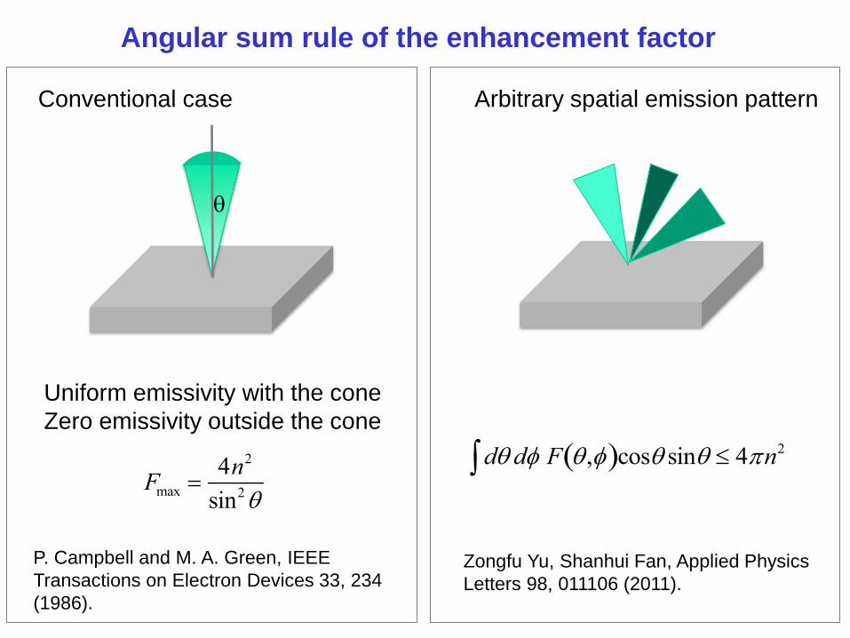
Angular sum rule of the enhancement factor
Uniform emissivity with the cone
Zero emissivity outside the cone
Zongfu Yu, Shanhui Fan, Applied Physics
Letters 98, 011106 (2011).
Fmax 4n2
sin2
Conventional case Arbitrary spatial emission pattern
d d F , cos sin 4n2
P. Campbell and M. A. Green, IEEE
Transactions on Electron Devices 33, 234
(1986).
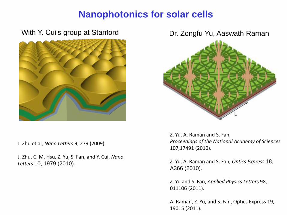
Nanophotonics for solar cells
Z. Yu, A. Raman and S. Fan, Proceedings of the National Academy of Sciences 107,17491 (2010). Z. Yu, A. Raman and S. Fan, Optics Express 18,
A366 (2010). Z. Yu and S. Fan, Applied Physics Letters 98, 011106 (2011). A. Raman, Z. Yu, and S. Fan, Optics Express 19, 19015 (2011).
J. Zhu et al, Nano Letters 9, 279 (2009). J. Zhu, C. M. Hsu, Z. Yu, S. Fan, and Y. Cui, Nano Letters 10, 1979 (2010).
With Y. Cui’s group at Stanford Dr. Zongfu Yu, Aaswath Raman

Photon as an important heat carrier
On earth From the sun

Improving Solar Cell Efficiency
P
N
V
Sun Semiconductor PN junction
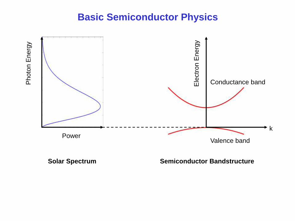
Basic Semiconductor Physics P
hoto
n E
nerg
y
Power
Solar Spectrum Semiconductor Bandstructure
Ele
ctr
on E
nerg
y
k
Valence band
Conductance band
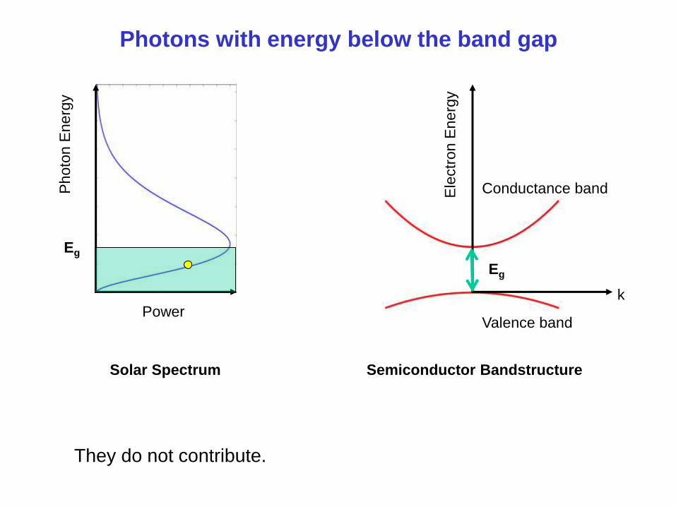
Photons with energy below the band gap P
hoto
n E
nerg
y
Power
Solar Spectrum Semiconductor Bandstructure
Ele
ctr
on E
nerg
y
k
Valence band
Conductance band
Eg
They do not contribute.
Eg
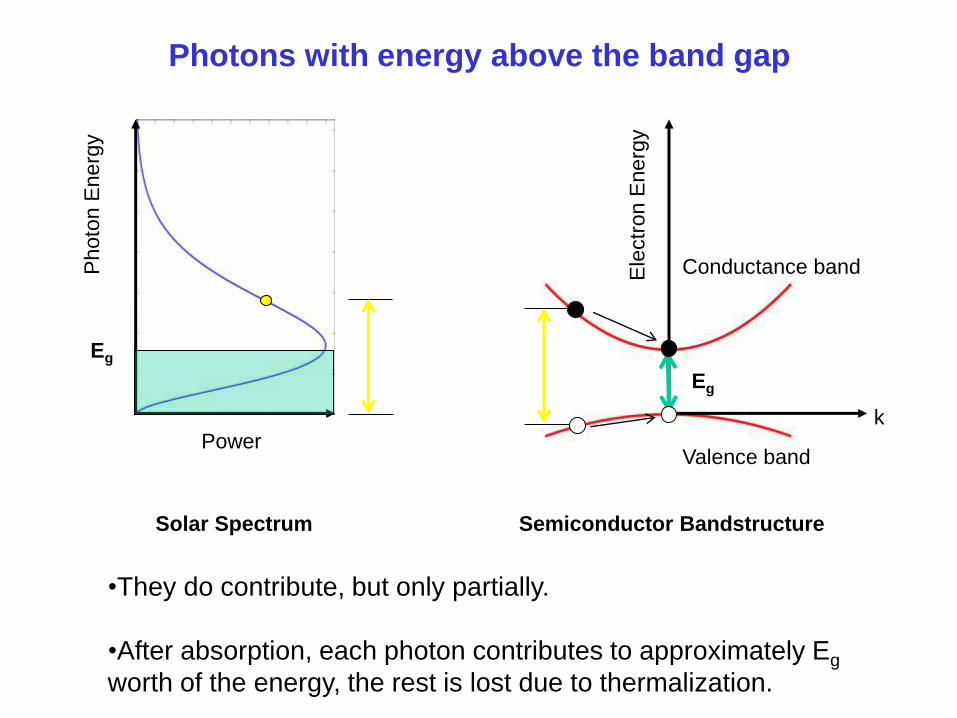
Photons with energy above the band gap P
hoto
n E
nerg
y
Power
Solar Spectrum Semiconductor Bandstructure
Ele
ctr
on E
nerg
y
k
Valence band
Conductance band
Eg
•They do contribute, but only partially.
•After absorption, each photon contributes to approximately Eg
worth of the energy, the rest is lost due to thermalization.
Eg
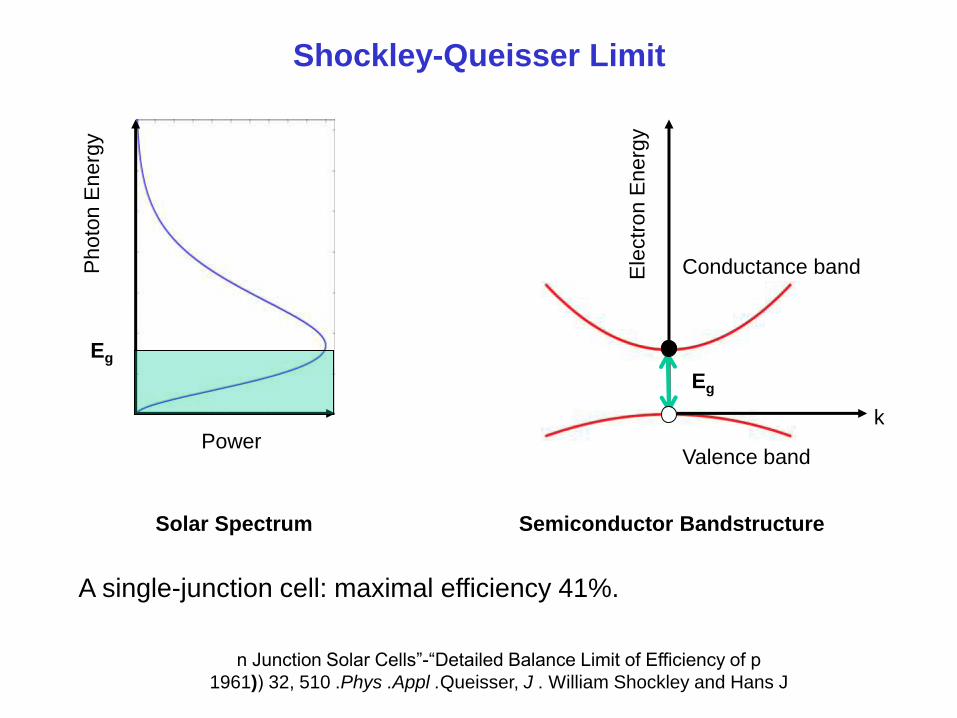
Shockley-Queisser Limit P
hoto
n E
nerg
y
Power
Solar Spectrum Semiconductor Bandstructure
Ele
ctr
on E
nerg
y
k
Valence band
Conductance band
Eg
A single-junction cell: maximal efficiency 41%.
Eg
“Detailed Balance Limit of Efficiency of p-n Junction Solar Cells”
William Shockley and Hans J .Queisser, J .Appl .Phys .32, 510 (1961)
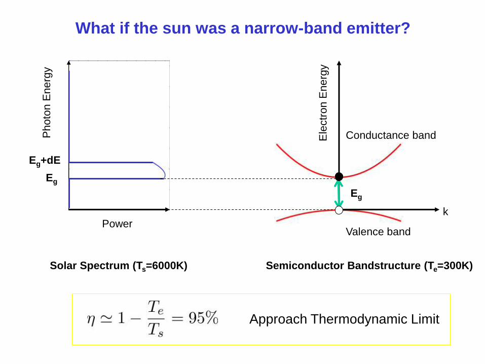
What if the sun was a narrow-band emitter? P
hoto
n E
nerg
y
Power
Solar Spectrum (Ts=6000K) Semiconductor Bandstructure (Te=300K)
Ele
ctr
on E
ne
rgy
k
Valence band
Conductance band
Eg
Eg
Eg+dE
Approach Thermodynamic Limit
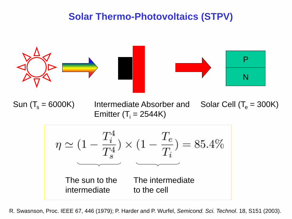
Solar Thermo-Photovoltaics (STPV)
Sun (Ts = 6000K)
P
N
Intermediate Absorber and
Emitter (Ti = 2544K)
Solar Cell (Te = 300K)
The sun to the
intermediate
The intermediate
to the cell
R. Swasnson, Proc. IEEE 67, 446 (1979); P. Harder and P. Wurfel, Semicond. Sci. Technol. 18, S151 (2003).
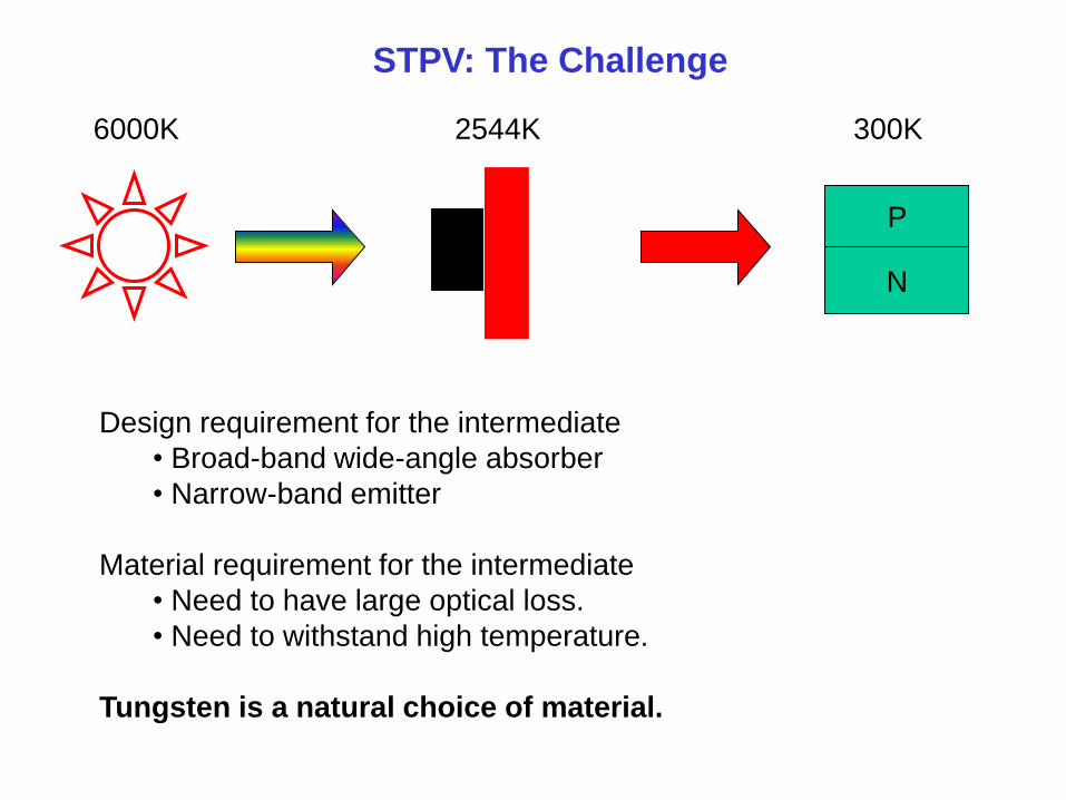
STPV: The Challenge
6000K
P
N
2544K 300K
Design requirement for the intermediate
• Broad-band wide-angle absorber
• Narrow-band emitter
Material requirement for the intermediate
• Need to have large optical loss.
• Need to withstand high temperature.
Tungsten is a natural choice of material.

Dielectric Function of Tungsten
Tungsten is a very lossy material in the solar wavelength range.
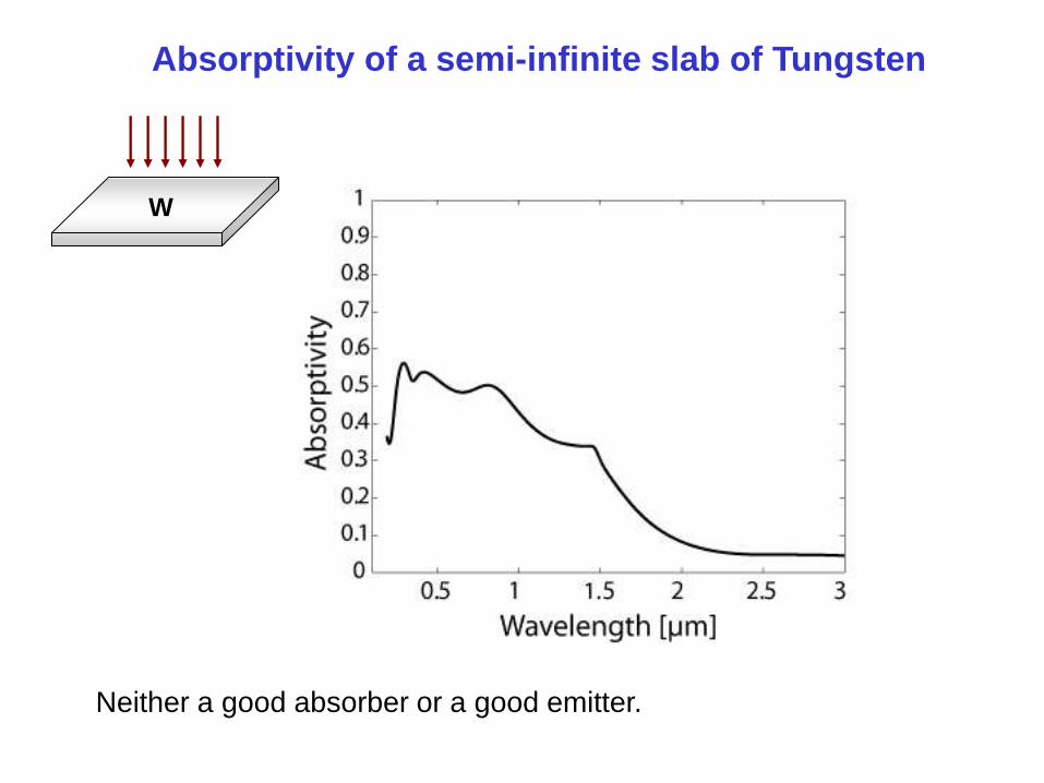
W
Absorptivity of a semi-infinite slab of Tungsten
Neither a good absorber or a good emitter.
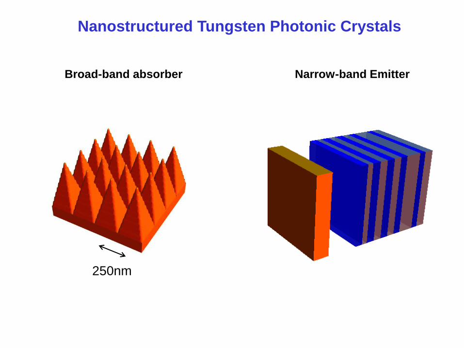
Nanostructured Tungsten Photonic Crystals
Narrow-band Emitter Broad-band absorber
250nm
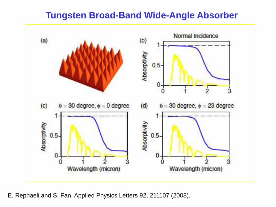
Tungsten Broad-Band Wide-Angle Absorber
E. Rephaeli and S. Fan, Applied Physics Letters 92, 211107 (2008).
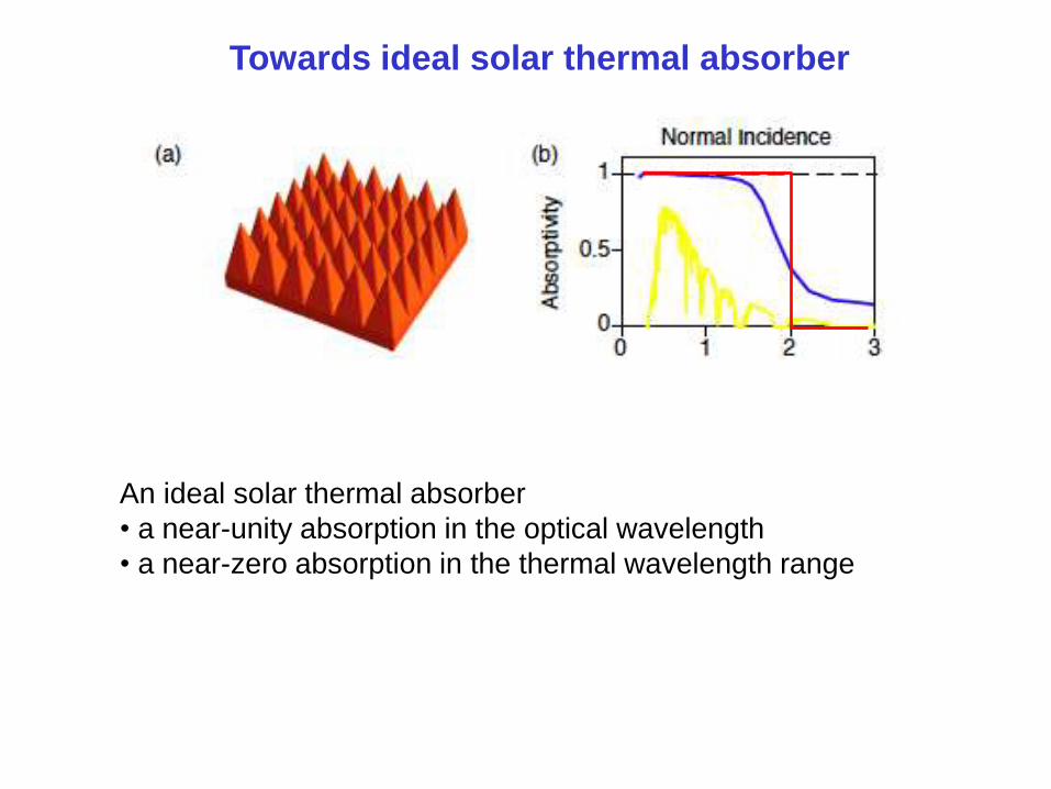
Towards ideal solar thermal absorber
An ideal solar thermal absorber
• a near-unity absorption in the optical wavelength
• a near-zero absorption in the thermal wavelength range
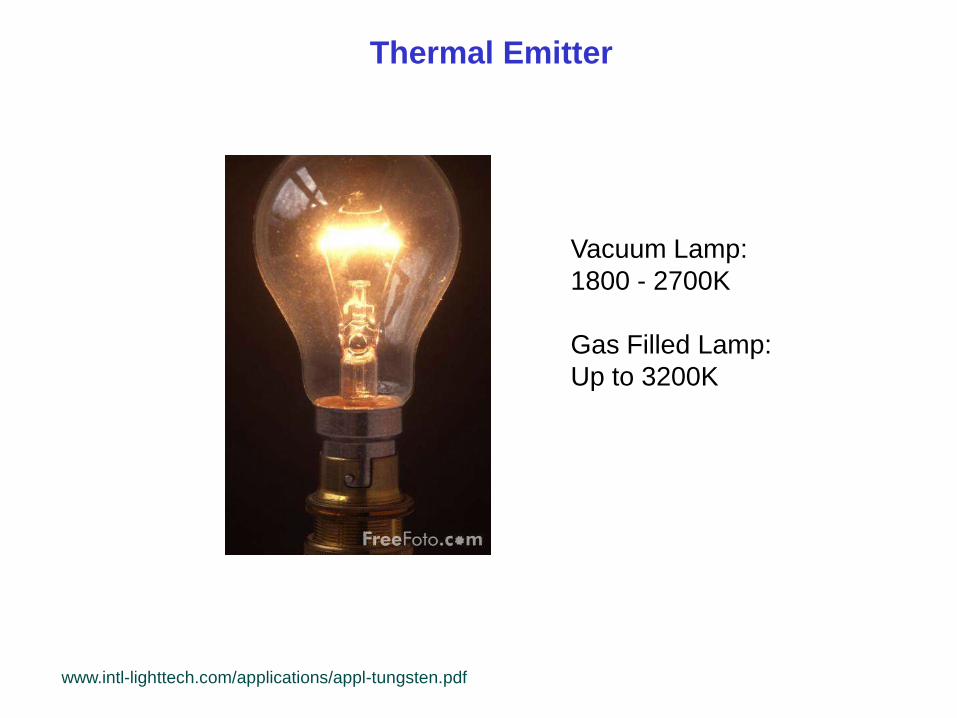
Thermal Emitter
Vacuum Lamp:
1800 - 2700K
Gas Filled Lamp:
Up to 3200K
www.intl-lighttech.com/applications/appl-tungsten.pdf
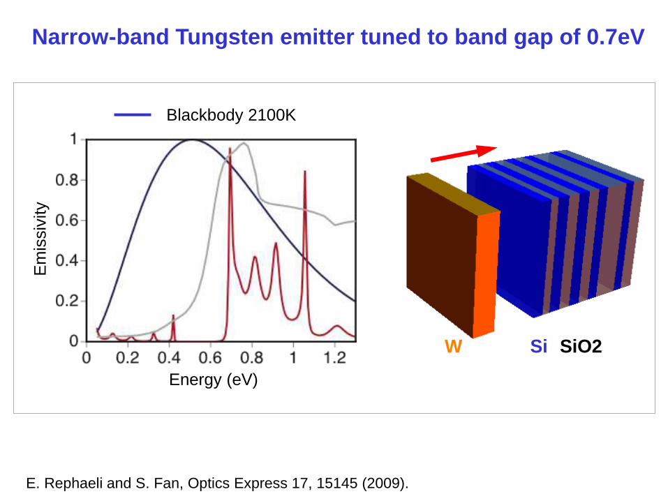
Narrow-band Tungsten emitter tuned to band gap of 0.7eV
Energy (eV)
Em
issiv
ity
Blackbody 2100K
W Si SiO2
E. Rephaeli and S. Fan, Optics Express 17, 15145 (2009).
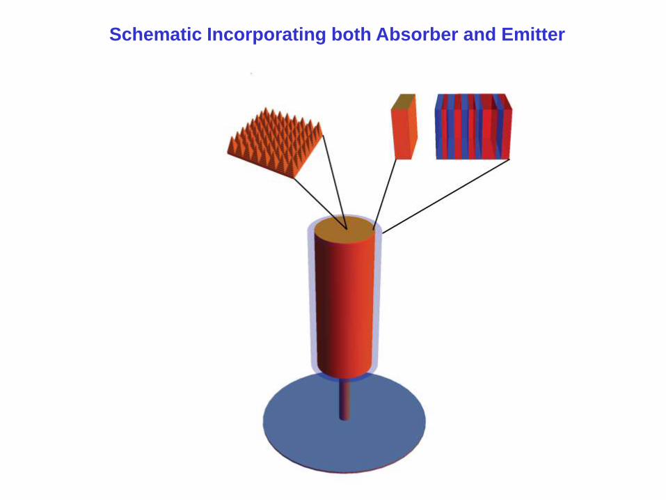
Schematic Incorporating both Absorber and Emitter
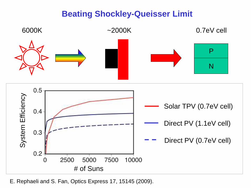
Beating Shockley-Queisser Limit
6000K
P
N
~2000K 0.7eV cell
E. Rephaeli and S. Fan, Optics Express 17, 15145 (2009).
Solar TPV (0.7eV cell)
Direct PV (1.1eV cell)
Direct PV (0.7eV cell)
# of Suns
Syste
m E
ffic
iency
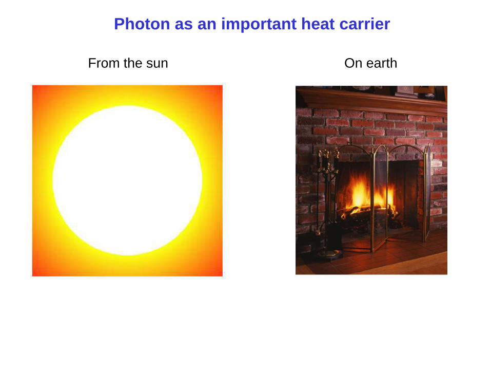
Photon as an important heat carrier
On earth From the sun
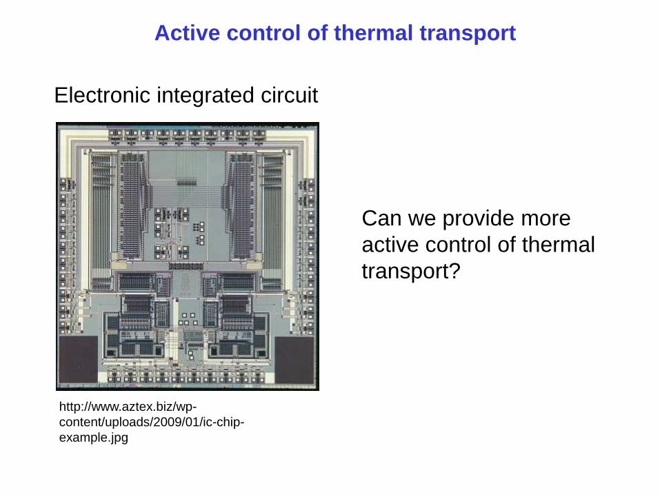
Active control of thermal transport
http://www.aztex.biz/wp-
content/uploads/2009/01/ic-chip-
example.jpg
Can we provide more
active control of thermal
transport?
Electronic integrated circuit
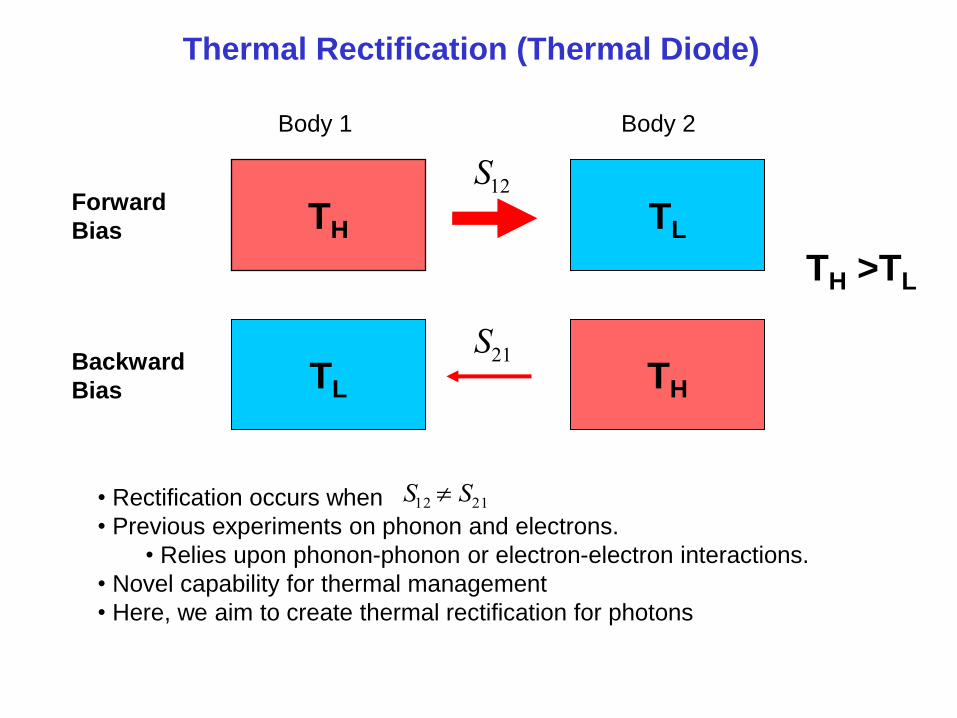
Thermal Rectification (Thermal Diode)
Body 1 Body 2
Forward
Bias
Backward
Bias
TH TL
TH TL
TH >TL
S12
S21
• Rectification occurs when
• Previous experiments on phonon and electrons.
• Relies upon phonon-phonon or electron-electron interactions.
• Novel capability for thermal management
• Here, we aim to create thermal rectification for photons
S12 S21
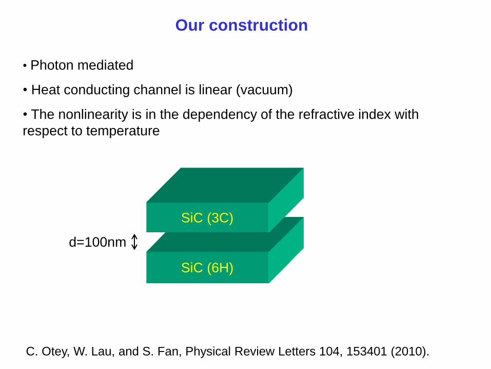
SiC (6H)
• Photon mediated
• Heat conducting channel is linear (vacuum)
• The nonlinearity is in the dependency of the refractive index with
respect to temperature
Our construction
SiC (3C)
d=100nm
C. Otey, W. Lau, and S. Fan, Physical Review Letters 104, 153401 (2010).
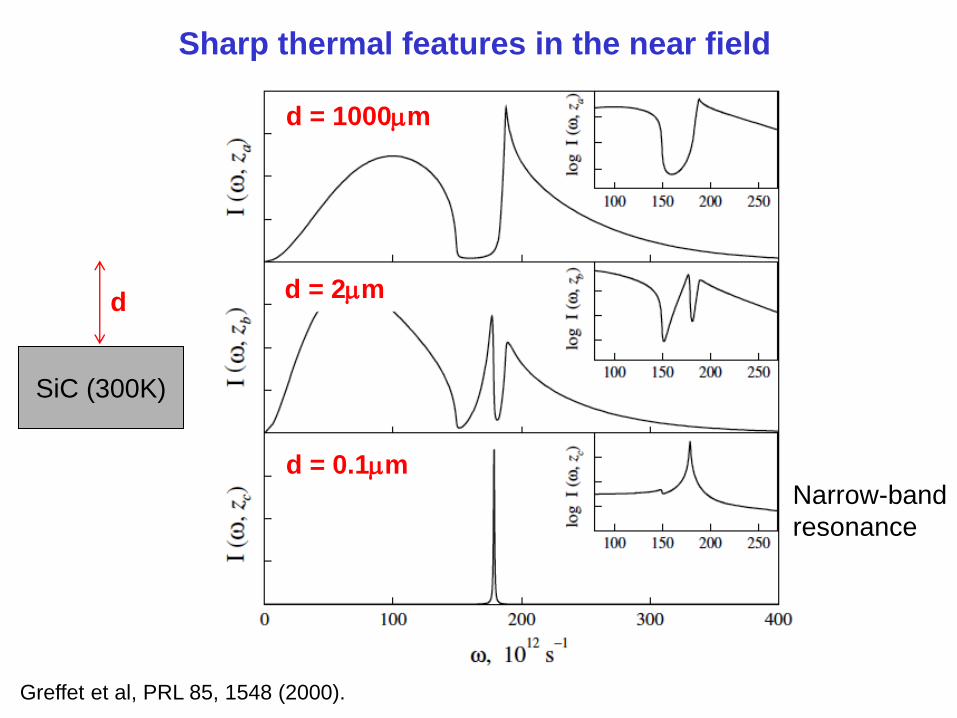
Sharp thermal features in the near field
SiC (300K)
d
Greffet et al, PRL 85, 1548 (2000).
d = 1000m
d = 2m
d = 0.1m Narrow-band
resonance
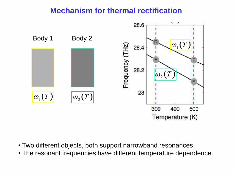
Mechanism for thermal rectification
Body 1 Body 2
• Two different objects, both support narrowband resonances
• The resonant frequencies have different temperature dependence.
1 T 2 T
1 T
2 T
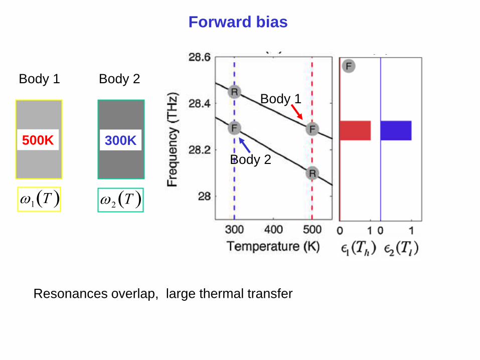
Forward bias
Body 1 Body 2
1 T 2 T
500K 300K
Resonances overlap, large thermal transfer
Body 1
Body 2
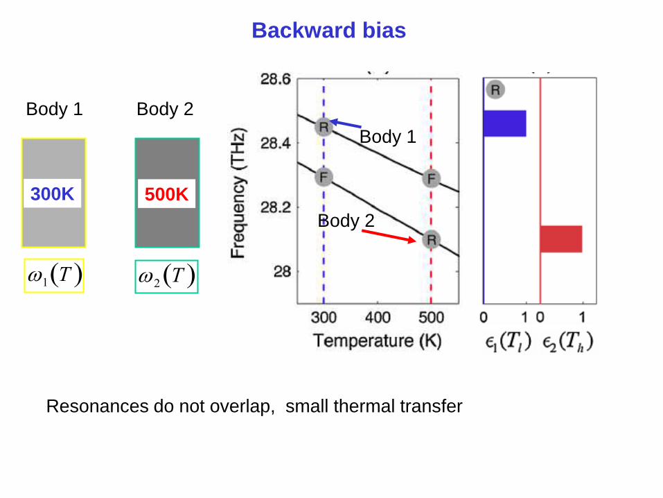
Backward bias
Body 1 Body 2
1 T 2 T
300K 500K
Body 1
Body 2
Resonances do not overlap, small thermal transfer
orward everse
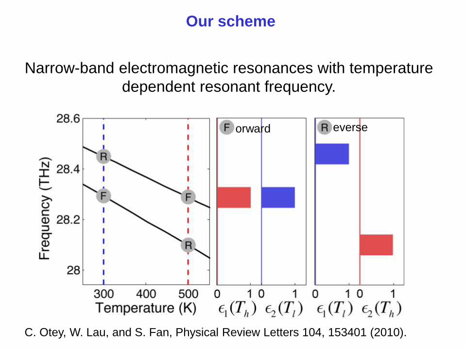
Narrow-band electromagnetic resonances with temperature
dependent resonant frequency.
Our scheme
C. Otey, W. Lau, and S. Fan, Physical Review Letters 104, 153401 (2010).
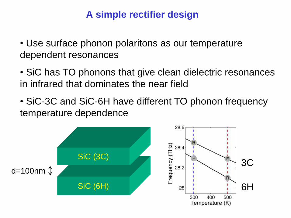
• Use surface phonon polaritons as our temperature
dependent resonances
• SiC has TO phonons that give clean dielectric resonances
in infrared that dominates the near field
• SiC-3C and SiC-6H have different TO phonon frequency
temperature dependence
3C
6H
A simple rectifier design
SiC (6H)
SiC (3C)
d=100nm
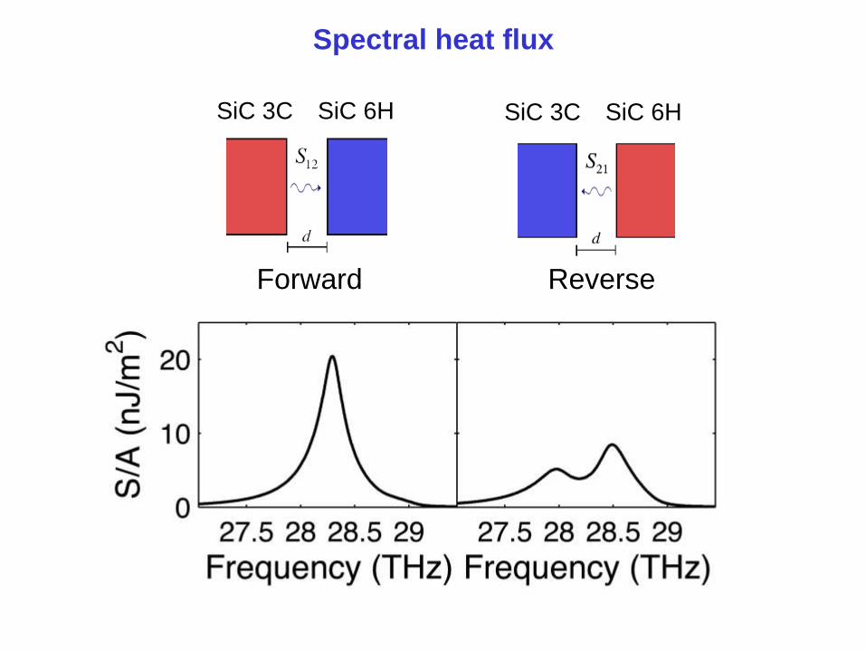
Forward Reverse
Spectral heat flux
SiC 3C SiC 6H SiC 3C SiC 6H
Rectification S12 S21
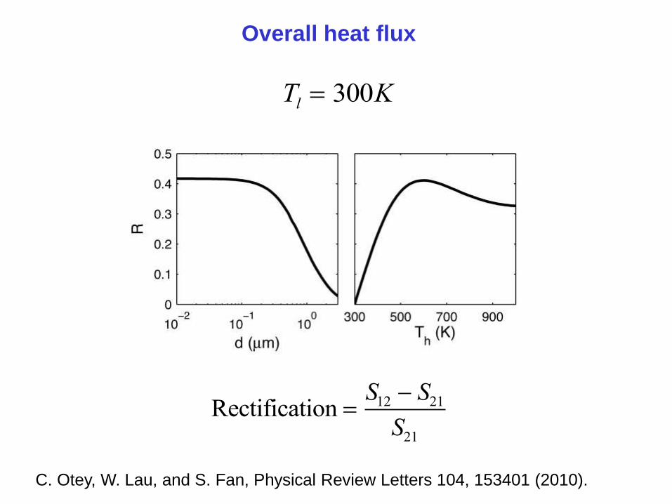
S21
Tl 300K
Overall heat flux
C. Otey, W. Lau, and S. Fan, Physical Review Letters 104, 153401 (2010).
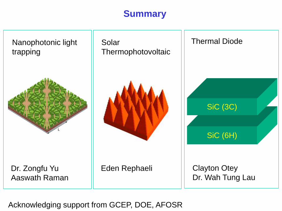
Summary
Nanophotonic light
trapping
Dr. Zongfu Yu
Aaswath Raman
SiC (6H)
SiC (3C)
Thermal Diode
Clayton Otey
Dr. Wah Tung Lau
Acknowledging support from GCEP, DOE, AFOSR
Eden Rephaeli
Solar
Thermophotovoltaic