fpga verification of alu - computer science & ejbakos/611/tutorials/tutorial14.pdffpga...
TRANSCRIPT
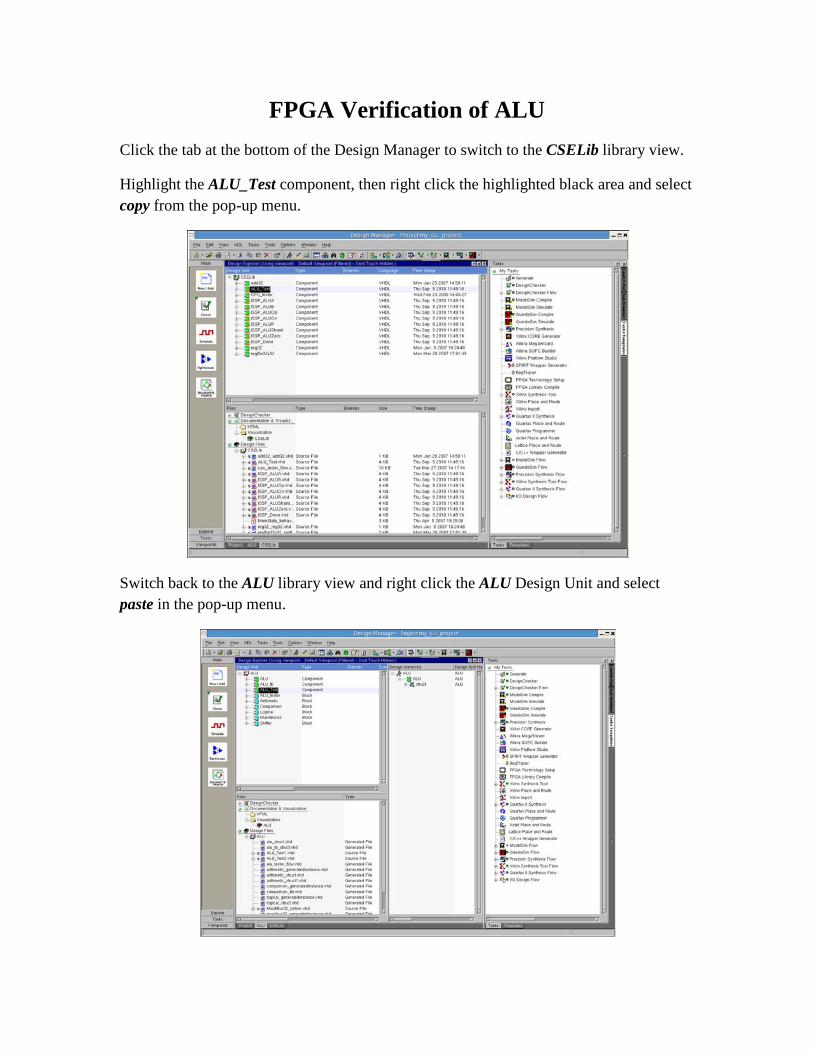
FPGA Verification of ALU Click the tab at the bottom of the Design Manager to switch to the CSELib library view.
Highlight the ALU_Test component, then right click the highlighted black area and select copy from the pop-up menu.
Switch back to the ALU library view and right click the ALU Design Unit and select paste in the pop-up menu.
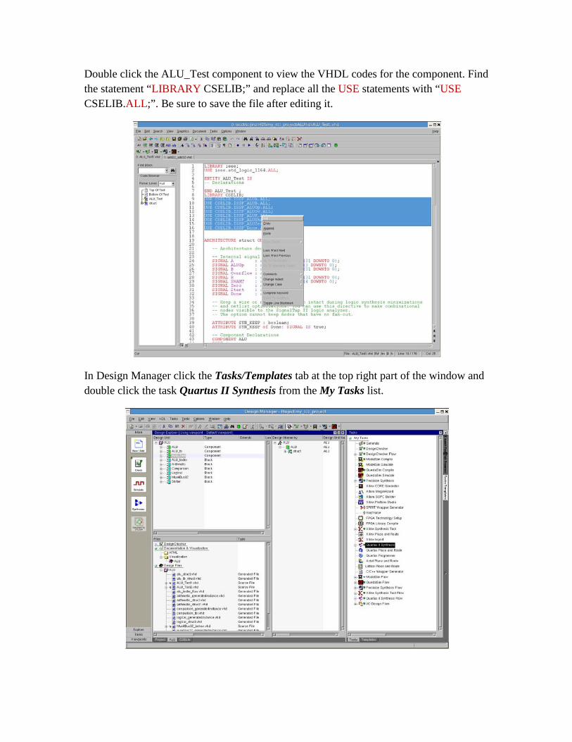
Double click the ALU_Test component to view the VHDL codes for the component. Find the statement “LIBRARY CSELIB;” and replace all the USE statements with “USE CSELIB.ALL;”. Be sure to save the file after editing it.
In Design Manager click the Tasks/Templates tab at the top right part of the window and double click the task Quartus II Synthesis from the My Tasks list.
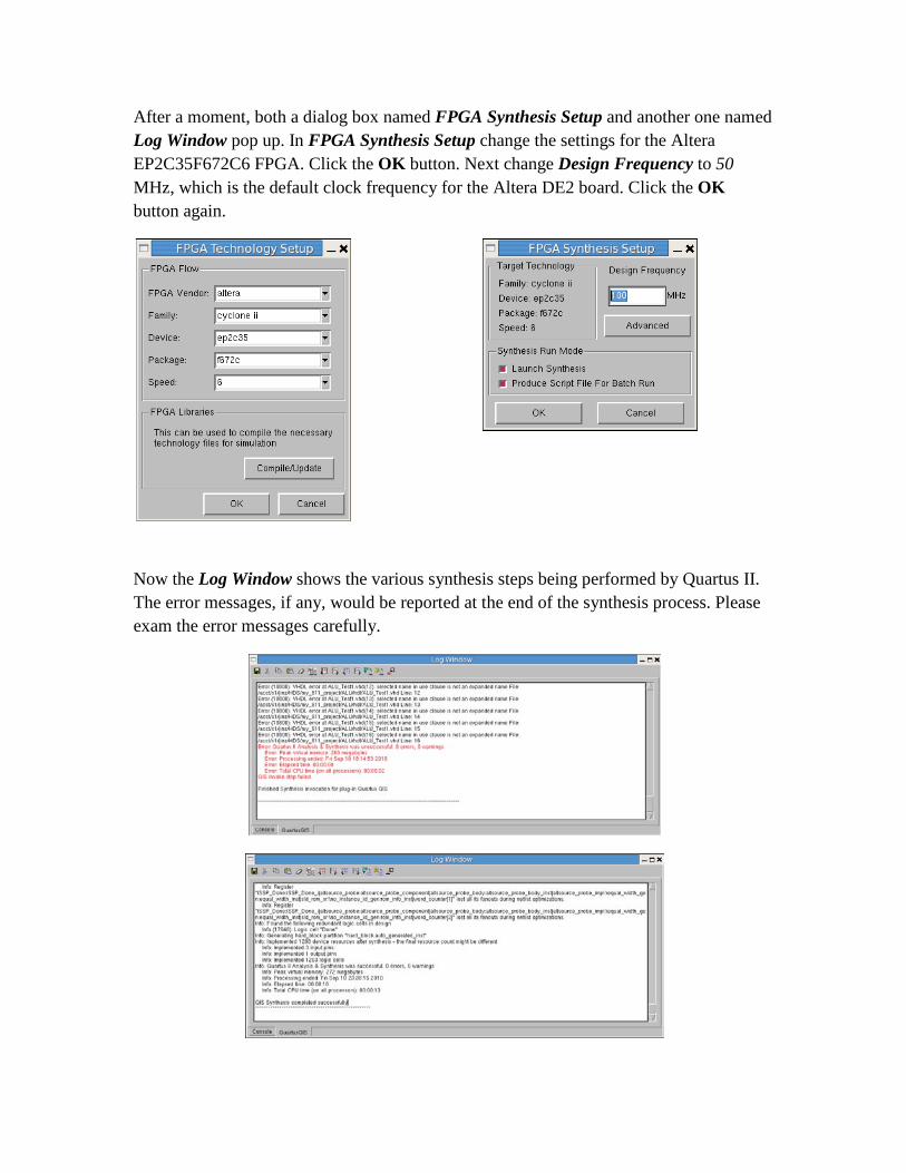
After a moment, both a dialog box named FPGA Synthesis Setup and another one named Log Window pop up. In FPGA Synthesis Setup change the settings for the Altera EP2C35F672C6 FPGA. Click the OK button. Next change Design Frequency to 50 MHz, which is the default clock frequency for the Altera DE2 board. Click the OK button again.
Now the Log Window shows the various synthesis steps being performed by Quartus II. The error messages, if any, would be reported at the end of the synthesis process. Please exam the error messages carefully.
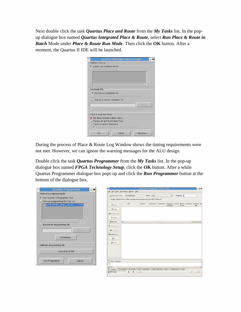
Next double click the task Quartus Place and Route from the My Tasks list. In the pop-up dialogue box named Quartus Integrated Place & Route, select Run Place & Route in Batch Mode under Place & Route Run Mode. Then click the OK button. After a moment, the Quartus II IDE will be launched.
During the process of Place & Route Log Window shows the timing requirements were not met. However, we can ignore the warning messages for the ALU design.
Double click the task Quartus Programmer from the My Tasks list. In the pop-up dialogue box named FPGA Technology Setup, click the OK button. After a while Quartus Programmer dialogue box pops up and click the Run Programmer button at the bottom of the dialogue box.
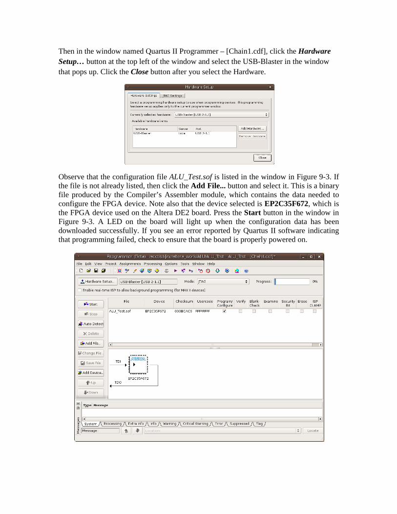
Then in the window named Quartus II Programmer – [Chain1.cdf], click the Hardware Setup… button at the top left of the window and select the USB-Blaster in the window that pops up. Click the Close button after you select the Hardware.
Observe that the configuration file ALU_Test.sof is listed in the window in Figure 9-3. If the file is not already listed, then click the Add File... button and select it. This is a binary file produced by the Compiler’s Assembler module, which contains the data needed to configure the FPGA device. Note also that the device selected is EP2C35F672, which is the FPGA device used on the Altera DE2 board. Press the Start button in the window in Figure 9-3. A LED on the board will light up when the configuration data has been downloaded successfully. If you see an error reported by Quartus II software indicating that programming failed, check to ensure that the board is properly powered on.
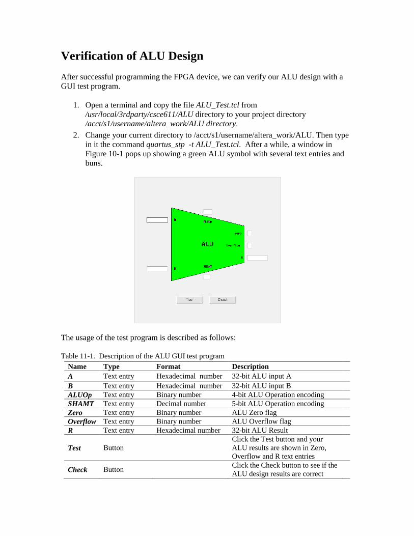
Verification of ALU Design After successful programming the FPGA device, we can verify our ALU design with a GUI test program.
1. Open a terminal and copy the file ALU_Test.tcl from /usr/local/3rdparty/csce611/ALU directory to your project directory /acct/s1/username/altera_work/ALU directory.
2. Change your current directory to /acct/s1/username/altera_work/ALU. Then type in it the command quartus_stp -t ALU_Test.tcl. After a while, a window in Figure 10-1 pops up showing a green ALU symbol with several text entries and buns.
The usage of the test program is described as follows: Table 11-1. Description of the ALU GUI test program
Name Type Format Description A Text entry Hexadecimal number 32-bit ALU input A B Text entry Hexadecimal number 32-bit ALU input B ALUOp Text entry Binary number 4-bit ALU Operation encoding SHAMT Text entry Decimal number 5-bit ALU Operation encoding Zero Text entry Binary number ALU Zero flag Overflow Text entry Binary number ALU Overflow flag R Text entry Hexadecimal number 32-bit ALU Result
Test Button Click the Test button and your ALU results are shown in Zero, Overflow and R text entries
Check Button Click the Check button to see if the ALU design results are correct

Make sure you follow the formats of the text entries. Otherwise, some ALU inputs may be set to 0 and a warning message is prompted. If you have problem with testing the ALU design, ask the instructors for help.
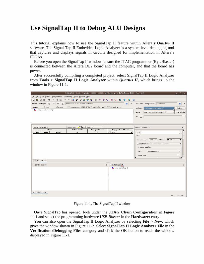
Use SignalTap II to Debug ALU Designs This tutorial explains how to use the SignalTap II feature within Altera’s Quartus II software. The Signal-Tap II Embedded Logic Analyzer is a system-level debugging tool that captures and displays signals in circuits designed for implementation in Altera’s FPGAs. Before you open the SignalTap II window, ensure the JTAG programmer (ByteBlaster) is connected between the Altera DE2 board and the computer, and that the board has power. After successfully compiling a completed project, select SignalTap II Logic Analyzer from Tools > SignalTap II Logic Analyzer within Quartus II, which brings up the window in Figure 11-1.
Figure 11-1. The SignalTap II window Once SignalTap has opened, look under the JTAG Chain Configuration in Figure 11-1 and select the programming hardware USB-Blaster in the Hardware: entry. You can also open the SignalTap II Logic Analyzer by selecting File > New, which gives the window shown in Figure 11-2. Select SignalTap II Logic Analyzer File in the Verification /Debugging Files category and click the OK button to reach the window displayed in Figure 11-1.
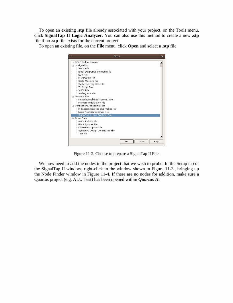
To open an existing .stp file already associated with your project, on the Tools menu, click SignalTap II Logic Analyzer. You can also use this method to create a new .stp file if no .stp file exists for the current project.
To open an existing file, on the File menu, click Open and select a .stp file
Figure 11-2. Choose to prepare a SignalTap II File. We now need to add the nodes in the project that we wish to probe. In the Setup tab of the SignalTap II window, right-click in the window shown in Figure 11-3., bringing up the Node Finder window in Figure 11-4. If there are no nodes for addition, make sure a Quartus project (e.g. ALU Test) has been opened within Quartus II.
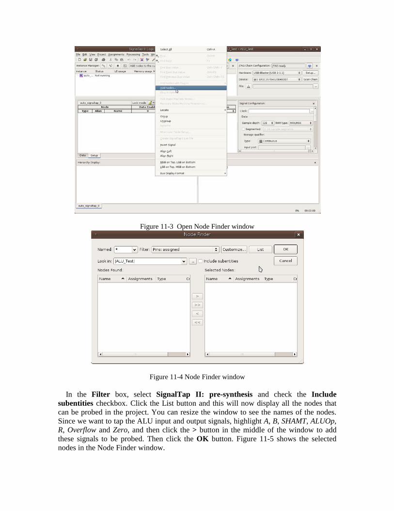
Figure 11-3 Open Node Finder window
Figure 11-4 Node Finder window In the Filter box, select SignalTap II: pre-synthesis and check the Include subentities checkbox. Click the List button and this will now display all the nodes that can be probed in the project. You can resize the window to see the names of the nodes. Since we want to tap the ALU input and output signals, highlight A, B, SHAMT, ALUOp, R, Overflow and Zero, and then click the > button in the middle of the window to add these signals to be probed. Then click the OK button. Figure 11-5 shows the selected nodes in the Node Finder window.
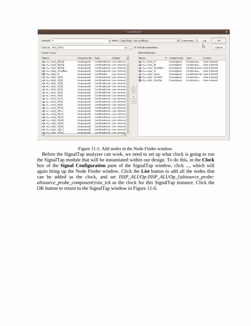
Figure 11-5. Add nodes in the Node Finder window. Before the SignalTap analyzer can work, we need to set up what clock is going to run the SignalTap module that will be instantiated within our design. To do this, in the Clock box of the Signal Configuration pane of the SignalTap window, click ..., which will again bring up the Node Finder window. Click the List button to add all the nodes that can be added as the clock, and set ISSP_ALUOp:ISSP_ALUOp_i|altsource_probe: altsource_probe_component|raw_tck as the clock for this SignalTap instance. Click the OK button to return to the SignalTap window in Figure 11-6.
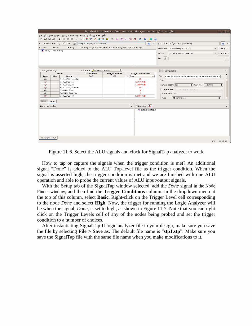
Figure 11-6. Select the ALU signals and clock for SignalTap analyzer to work How to tap or capture the signals when the trigger condition is met? An additional signal “Done” is added to the ALU Top-level file as the trigger condition. When the signal is asserted high, the trigger condition is met and we are finished with one ALU operation and able to probe the current values of ALU input/output signals. With the Setup tab of the SignalTap window selected, add the Done signal in the Node Finder window, and then find the Trigger Conditions column. In the dropdown menu at the top of this column, select Basic. Right-click on the Trigger Level cell corresponding to the node Done and select High. Now, the trigger for running the Logic Analyzer will be when the signal, Done, is set to high, as shown in Figure 11-7. Note that you can right click on the Trigger Levels cell of any of the nodes being probed and set the trigger condition to a number of choices. After instantiating SignalTap II logic analyzer file in your design, make sure you save the file by selecting File > Save as. The default file name is “stp1.stp”. Make sure you save the SignalTap file with the same file name when you make modifications to it.
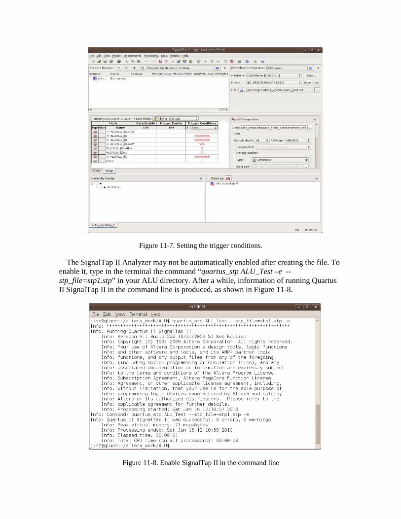
Figure 11-7. Setting the trigger conditions.
The SignalTap II Analyzer may not be automatically enabled after creating the file. To enable it, type in the terminal the command “quartus_stp ALU_Test –e --stp_file=stp1.stp” in your ALU directory. After a while, information of running Quartus II SignalTap II in the command line is produced, as shown in Figure 11-8.
Figure 11-8. Enable SignalTap II in the command line
The last step is to compile the design. Click on the toolbar icon and start compilation. After compilation, use the toolbar icon to load the project onto the DE2 board. The compiler may display some warning messages, but make sure Quartus II Analysis & Synthesis was successful with 0 errors and 0 warnings. If you have trouble with the compilation of the project, please ask the instructors for help. 12. Probing the Design Using SignalTap II Now that the project with SignalTap II instantiated has been loaded onto the DE2 board, we can now probe the nodes as we would with an external logic analyzer.
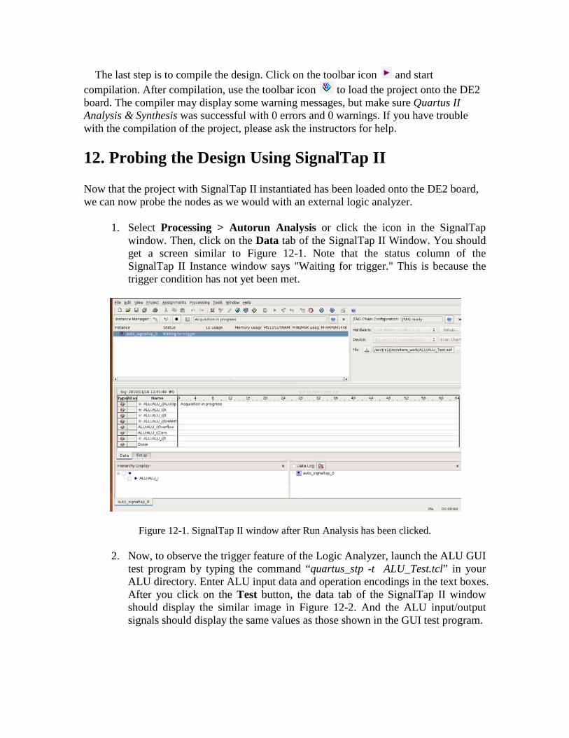
1. Select Processing > Autorun Analysis or click the icon in the SignalTap window. Then, click on the Data tab of the SignalTap II Window. You should get a screen similar to Figure 12-1. Note that the status column of the SignalTap II Instance window says "Waiting for trigger." This is because the trigger condition has not yet been met.
Figure 12-1. SignalTap II window after Run Analysis has been clicked.
2. Now, to observe the trigger feature of the Logic Analyzer, launch the ALU GUI test program by typing the command “quartus_stp -t ALU_Test.tcl” in your ALU directory. Enter ALU input data and operation encodings in the text boxes. After you click on the Test button, the data tab of the SignalTap II window should display the similar image in Figure 12-2. And the ALU input/output signals should display the same values as those shown in the GUI test program.
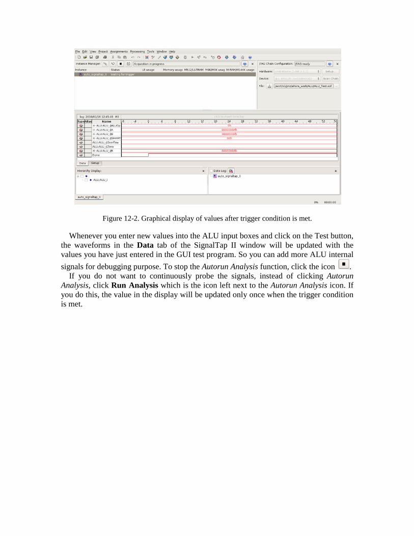
Figure 12-2. Graphical display of values after trigger condition is met. Whenever you enter new values into the ALU input boxes and click on the Test button, the waveforms in the Data tab of the SignalTap II window will be updated with the values you have just entered in the GUI test program. So you can add more ALU internal signals for debugging purpose. To stop the Autorun Analysis function, click the icon .
If you do not want to continuously probe the signals, instead of clicking Autorun Analysis, click Run Analysis which is the icon left next to the Autorun Analysis icon. If you do this, the value in the display will be updated only once when the trigger condition is met.