nanoscientific - parksystems.com · works in the field of nanotechnology, nano science, ... the...
TRANSCRIPT

SUB-ANGSTROM ROUGHNESS
REPEATABILITYWITH TIP-TO-TIP
CORRELATION. p. 10
EXAMINING CELL ION CHANNELS USING INNOVATIVE TARGETED PATCH CLAMPING ON ION CONDUCTANCE MICROSCOPYp. 13
NANOscientificWINTER 2014 The Magazine for Nanotechnology
INTERVIEW: TCELL VISUALIZATION AND
MANIPULATION USING ATOMIC FORCE MICROSCOPY
AN INTERVIEW WITH DR. MANISH BUTTE
p. 18
NANOSCALE CHARACTERIZATION
FOR OIL & GAS INDUSTRY
AN INTERVIEW WITH DR. RIGOBERTO ADVINCULA
p. 8
SMARTSCAN BY PARK SYSTEM
PROFESSIONAL AFM IMAGES WITH A SINGLE CLICK
p. 6
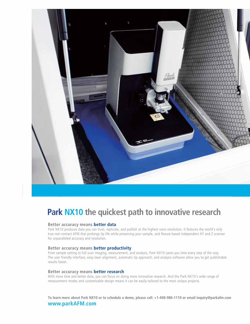

TABLE OF CONTENTS Message from Editor/NanoTechnology News Update 5 Feature Article: SmartScan Professional AFM images with a Single Click 7 Feature Story: Nanoscale Characterization for Oil & Gas Industry An Interview with Dr. Rigoberto Advincula, Professor Department of Macromolecular Science and Engineering Case Western University 10 Feature Story: Sub-Angstrom Roughness Repeatability with Tip-to-Tip Correlation. Ardavan Zandiatashbar 14 Feature Interview: Dr. Manish Butte, Asst Professor Pediatrics, Immunology and Allergy. Stanford School of Medicine. Critical Role of Atomic Force Microscopes in Conducting T Cell Research At Stanford School of Medicine 17 Examining Cell Ion Channels Using Innovative Targeted Patch Clamping on Ion Conductance Microscopy MyungHoon Choi, Goo Eun Jung 20 Park Systems News Update 22
NANOscientific The Magazine for Nanotechnology
www.nano-scientific.org
Keibock Lee, Editor-in-Chief [email protected]
Deborah West, Content Editor [email protected]
Art Director, Ryan Mackenzie
Gerard Pascal, Digital Media & Advertising Manager [email protected]
Published by Park Systems, Inc.3040 Olcott St. Santa, Clara CA [email protected], 408-986-1110www.parkAFM.com
NANOscientific is published quarterly to showcase advancements in the field of nano science and technology across a wide range of multidisciplinary areas of research.
The publication is offered free to anyone who works in the field of Nanotechnology, Nano Science, Microscopy and other related fields of study and manufacturing.
For inquiries about submitting story ideas, please contact Deborah West, Content Editor at [email protected] for inquiries about Advertising in NANOscientific, please contact Gerald Pascal at [email protected]
p. 7
p. 10
p. 14
p. 18
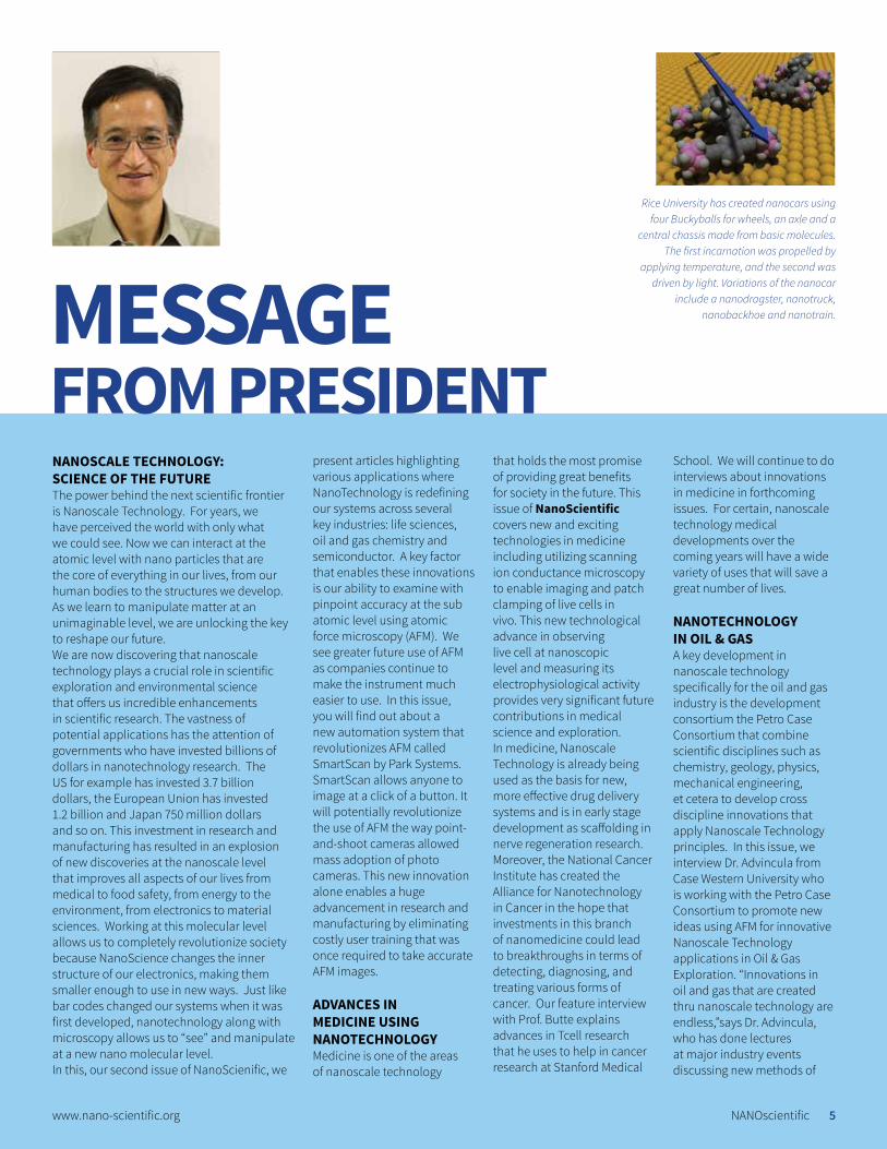
NANOSCALE TECHNOLOGY: SCIENCE OF THE FUTUREThe power behind the next scientific frontier is Nanoscale Technology. For years, we have perceived the world with only what we could see. Now we can interact at the atomic level with nano particles that are the core of everything in our lives, from our human bodies to the structures we develop. As we learn to manipulate matter at an unimaginable level, we are unlocking the key to reshape our future.We are now discovering that nanoscale technology plays a crucial role in scientific exploration and environmental science that offers us incredible enhancements in scientific research. The vastness of potential applications has the attention of governments who have invested billions of dollars in nanotechnology research. The US for example has invested 3.7 billion dollars, the European Union has invested 1.2 billion and Japan 750 million dollars and so on. This investment in research and manufacturing has resulted in an explosion of new discoveries at the nanoscale level that improves all aspects of our lives from medical to food safety, from energy to the environment, from electronics to material sciences. Working at this molecular level allows us to completely revolutionize society because NanoScience changes the inner structure of our electronics, making them smaller enough to use in new ways. Just like bar codes changed our systems when it was first developed, nanotechnology along with microscopy allows us to “see” and manipulate at a new nano molecular level. In this, our second issue of NanoScienific, we
present articles highlighting various applications where NanoTechnology is redefining our systems across several key industries: life sciences, oil and gas chemistry and semiconductor. A key factor that enables these innovations is our ability to examine with pinpoint accuracy at the sub atomic level using atomic force microscopy (AFM). We see greater future use of AFM as companies continue to make the instrument much easier to use. In this issue, you will find out about a new automation system that revolutionizes AFM called SmartScan by Park Systems. SmartScan allows anyone to image at a click of a button. It will potentially revolutionize the use of AFM the way point-and-shoot cameras allowed mass adoption of photo cameras. This new innovation alone enables a huge advancement in research and manufacturing by eliminating costly user training that was once required to take accurate AFM images.
ADVANCES IN MEDICINE USING NANOTECHNOLOGYMedicine is one of the areas of nanoscale technology
that holds the most promise of providing great benefits for society in the future. This issue of NanoScientific covers new and exciting technologies in medicine including utilizing scanning ion conductance microscopy to enable imaging and patch clamping of live cells in vivo. This new technological advance in observing live cell at nanoscopic level and measuring its electrophysiological activity provides very significant future contributions in medical science and exploration.In medicine, Nanoscale Technology is already being used as the basis for new, more effective drug delivery systems and is in early stage development as scaffolding in nerve regeneration research. Moreover, the National Cancer Institute has created the Alliance for Nanotechnology in Cancer in the hope that investments in this branch of nanomedicine could lead to breakthroughs in terms of detecting, diagnosing, and treating various forms of cancer. Our feature interview with Prof. Butte explains advances in Tcell research that he uses to help in cancer research at Stanford Medical
School. We will continue to do interviews about innovations in medicine in forthcoming issues. For certain, nanoscale technology medical developments over the coming years will have a wide variety of uses that will save a great number of lives.
NANOTECHNOLOGY IN OIL & GASA key development in nanoscale technology specifically for the oil and gas industry is the development consortium the Petro Case Consortium that combine scientific disciplines such as chemistry, geology, physics, mechanical engineering, et cetera to develop cross discipline innovations that apply Nanoscale Technology principles. In this issue, we interview Dr. Advincula from Case Western University who is working with the Petro Case Consortium to promote new ideas using AFM for innovative Nanoscale Technology applications in Oil & Gas Exploration. “Innovations in oil and gas that are created thru nanoscale technology are endless,”says Dr. Advincula, who has done lectures at major industry events discussing new methods of
MESSAGEFROM PRESIDENT
Rice University has created nanocars using four Buckyballs for wheels, an axle and a
central chassis made from basic molecules. The first incarnation was propelled by
applying temperature, and the second was driven by light. Variations of the nanocar
include a nanodragster, nanotruck, nanobackhoe and nanotrain.
NANOscientificwww.nano-scientific.org 5
Keibock Lee, President of Park America
Nanoscale Characterization of Polymers and Chemicals that enhance oil & gas production while also being more environmentally conscious.
INNOVATIONS IN RESEARCH AT MAJOR UNIVERSITIESNanoscale technology is moving from science fiction into really hard engineering. We are seeing this as new products come out of research being done at so many major universities world-wide and in the curriculum at the schools that offer courses in NanoTechnology, creating young scientists who can continue to foster new innovationMany industry groups fund research projects of particular value to the industry at universities, labs and companies around the world. Projects can involve university research staff and industry representatives. Almost all of the leading discoveries in Nanoscale Technology begin with research projects at universities across the country where NanoTechnology classes are changing our science curriculum. For instance, Rice University in Houston,TX offers a Nanotechnology 101 course for business people and a short course on the history of the Buckyball (Buckminsterfullerene), which turns 25 in October. The Buckyball, which won a Nobel Prize in chemistry for Richard E. Smalley and his associates, measures only a single nanometer in diameter, yet its 60 carbon atom structure is tremendously strong, relying entirely on carbon-carbon bonds, which Adams says is the strongest of all possible elemental bonds. The single-walled carbon nanotube is essentially a continuous Buckyball.
Several years ago, Tour and his students at Rice University also created a nanocar, a nanotruck and a nanotrain using Buckyball wheels, axles and a tiny chassis. These nanovehicles were powered using a molecular motor that produced 1.8 rotations a minute.As industries come together and tackle all the challenges and opportunities this new field provides, we expect to see revolutionary changes. The future possibilities in NanoScale innovation are seemingly endless, and NanoScientific is here to share new innovations as they rapidly become part of our new science and manufacturing and providing new exciting ways to enhance our lives. I wish you all a very happy holiday season and I hope you enjoy our new issue. As always, I welcome your ideas and if you have an article you would like to submit, please forward it to us.
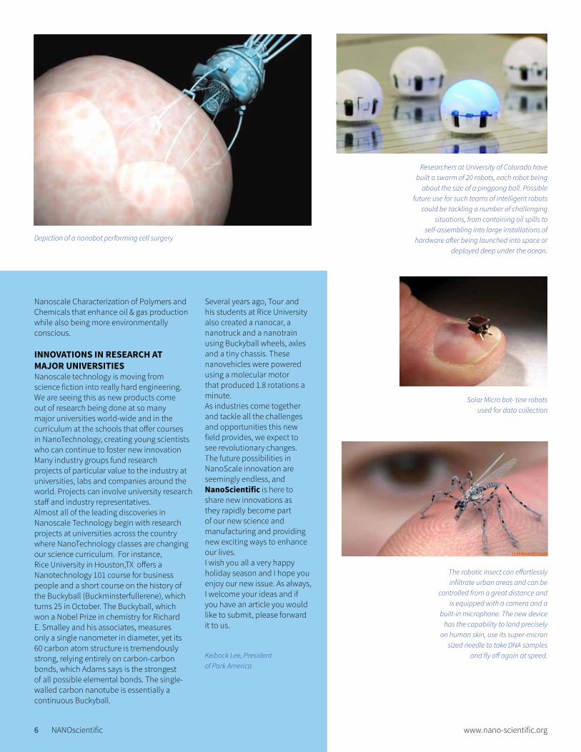
Depiction of a nanobot performing cell surgery
Researchers at University of Colorado have built a swarm of 20 robots, each robot being
about the size of a pingpong ball. Possible future use for such teams of intelligent robots
could be tackling a number of challenging situations, from containing oil spills to
self-assembling into large installations of hardware after being launched into space or
deployed deep under the ocean.
Solar Micro bot- tine robots used for data collection
The robotic insect can effortlessly infiltrate urban areas and can be
controlled from a great distance and is equipped with a camera and a
built-in microphone. The new device has the capability to land precisely
on human skin, use its super-micron sized needle to take DNA samples
and fly off again at speed.
NANOscientific www.nano-scientific.org6
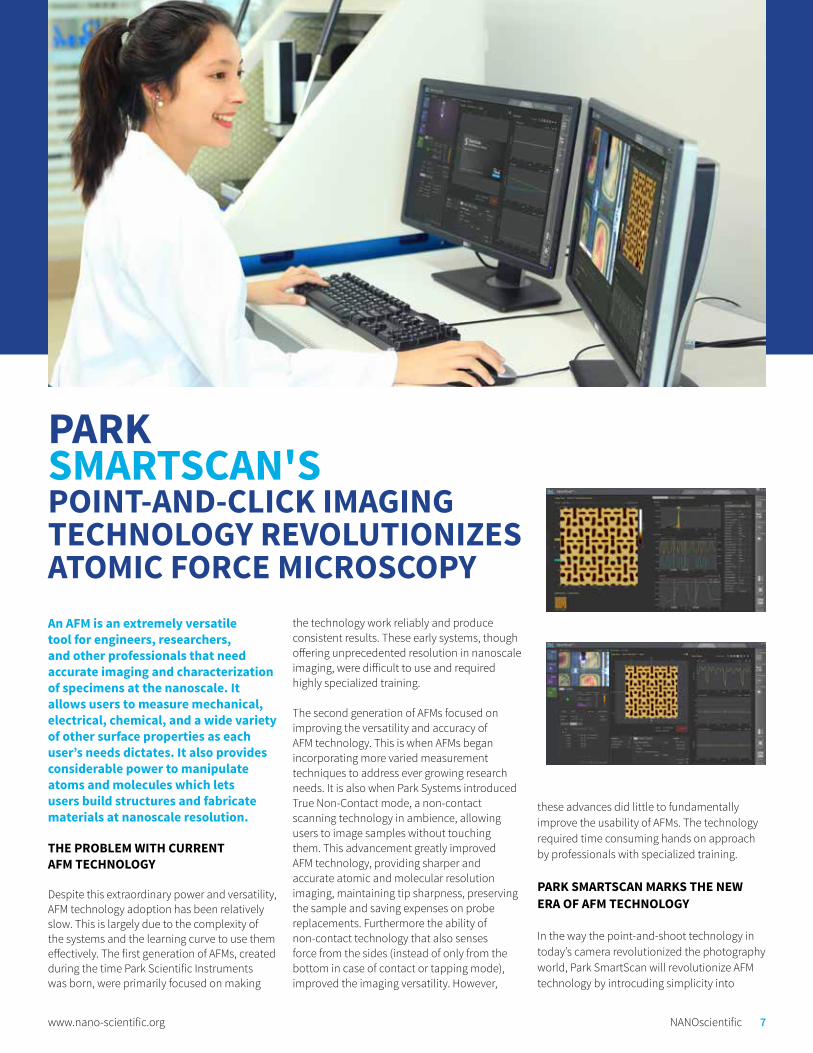
PARK SMARTSCAN'SPOINT-AND-CLICK IMAGING TECHNOLOGY REVOLUTIONIZES ATOMIC FORCE MICROSCOPY An AFM is an extremely versatile tool for engineers, researchers, and other professionals that need accurate imaging and characterization of specimens at the nanoscale. It allows users to measure mechanical, electrical, chemical, and a wide variety of other surface properties as each user’s needs dictates. It also provides considerable power to manipulate atoms and molecules which lets users build structures and fabricate materials at nanoscale resolution.
THE PROBLEM WITH CURRENT AFM TECHNOLOGY
Despite this extraordinary power and versatility, AFM technology adoption has been relatively slow. This is largely due to the complexity of the systems and the learning curve to use them effectively. The first generation of AFMs, created during the time Park Scientific Instruments was born, were primarily focused on making
the technology work reliably and produce consistent results. These early systems, though offering unprecedented resolution in nanoscale imaging, were difficult to use and required highly specialized training.
The second generation of AFMs focused on improving the versatility and accuracy of AFM technology. This is when AFMs began incorporating more varied measurement techniques to address ever growing research needs. It is also when Park Systems introduced True Non-Contact mode, a non-contact scanning technology in ambience, allowing users to image samples without touching them. This advancement greatly improved AFM technology, providing sharper and accurate atomic and molecular resolution imaging, maintaining tip sharpness, preserving the sample and saving expenses on probe replacements. Furthermore the ability of non-contact technology that also senses force from the sides (instead of only from the bottom in case of contact or tapping mode), improved the imaging versatility. However,
these advances did little to fundamentally improve the usability of AFMs. The technology required time consuming hands on approach by professionals with specialized training.
PARK SMARTSCAN MARKS THE NEW ERA OF AFM TECHNOLOGY
In the way the point-and-shoot technology in today’s camera revolutionized the photography world, Park SmartScan will revolutionize AFM technology by introcuding simplicity into
NANOscientific 7www.nano-scientific.org
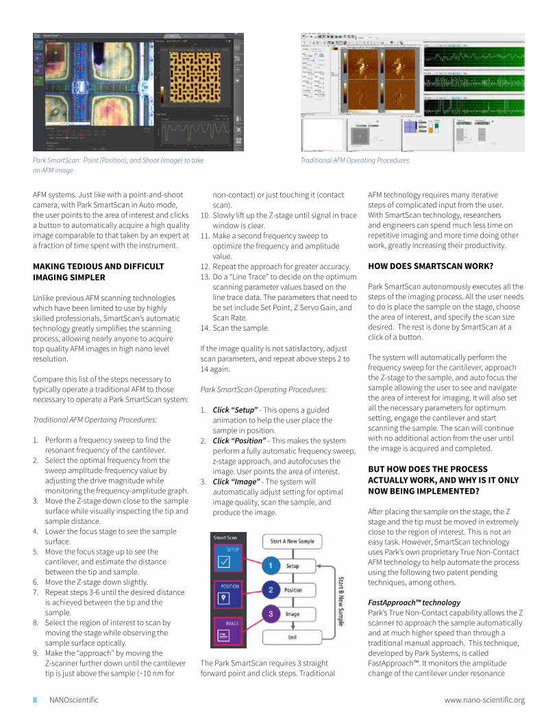
AFM systems. Just like with a point-and-shoot camera, with Park SmartScan in Auto mode, the user points to the area of interest and clicks a button to automatically acquire a high quality image comparable to that taken by an expert at a fraction of time spent with the instrument.
MAKING TEDIOUS AND DIFFICULT IMAGING SIMPLER
Unlike previous AFM scanning technologies which have been limited to use by highly skilled professionals, SmartScan’s automatic technology greatly simplifies the scanning process, allowing nearly anyone to acquire top quality AFM images in high nano level resolution.
Compare this list of the steps necessary to typically operate a traditional AFM to those necessary to operate a Park SmartScan system:
Traditional AFM Opertaing Procedures:
1. Perform a frequency sweep to find the resonant frequency of the cantilever.
2. Select the optimal frequency from the sweep amplitude-frequency value by adjusting the drive magnitude while monitoring the frequency-amplitude graph.
3. Move the Z-stage down close to the sample surface while visually inspecting the tip and sample distance.
4. Lower the focus stage to see the sample surface.
5. Move the focus stage up to see the cantilever, and estimate the distance between the tip and sample.
6. Move the Z-stage down slightly. 7. Repeat steps 3-6 until the desired distance
is achieved between the tip and the sample.
8. Select the region of interest to scan by moving the stage while observing the sample surface optically.
9. Make the “approach” by moving the Z-scanner further down until the cantilever tip is just above the sample (~10 nm for
non-contact) or just touching it (contact scan).
10. Slowly lift up the Z-stage until signal in trace window is clear.
11. Make a second frequency sweep to optimize the frequency and amplitude value.
12. Repeat the approach for greater accuracy.13. Do a “Line Trace” to decide on the optimum
scanning parameter values based on the line trace data. The parameters that need to be set include Set Point, Z Servo Gain, and Scan Rate.
14. Scan the sample.
If the image quality is not satisfactory, adjust scan parameters, and repeat above steps 2 to 14 again. Park SmartScan Operating Procedures:
1. Click “Setup” - This opens a guided animation to help the user place the sample in position.
2. Click “Position” - This makes the system perform a fully automatic frequency sweep, z-stage approach, and autofocuses the image. User points the area of interest.
3. Click “Image” - The system will automatically adjust setting for optimal image quality, scan the sample, and produce the image.
The Park SmartScan requires 3 straight forward point and click steps. Traditional
AFM technology requires many iterative steps of complicated input from the user. With SmartScan technology, researchers and engineers can spend much less time on repetitive imaging and more time doing other work, greatly increasing their productivity.
HOW DOES SMARTSCAN WORK?
Park SmartScan autonomously executes all the steps of the imaging process. All the user needs to do is place the sample on the stage, choose the area of interest, and specify the scan size desired. The rest is done by SmartScan at a click of a button.
The system will automatically perform the frequency sweep for the cantilever, approach the Z-stage to the sample, and auto focus the sample allowing the user to see and navigate the area of interest for imaging. It will also set all the necessary parameters for optimum setting, engage the cantilever and start scanning the sample. The scan will continue with no additional action from the user until the image is acquired and completed.
BUT HOW DOES THE PROCESS ACTUALLY WORK, AND WHY IS IT ONLY NOW BEING IMPLEMENTED?
After placing the sample on the stage, the Z stage and the tip must be moved in extremely close to the region of interest. This is not an easy task. However, SmartScan technology uses Park’s own proprietary True Non-Contact AFM technology to help automate the process using the following two patent pending techniques, among others.
FastApproach™ technologyPark’s True Non-Contact capability allows the Z scanner to approach the sample automatically and at much higher speed than through a traditional manual approach. This technique, developed by Park Systems, is called FastApproach™. It monitors the amplitude change of the cantilever under resonance
Park SmartScan: Point (Position), and Shoot (Image) to take an AFM image
Traditional AFM Operating Procedures
8 NANOscientific www.nano-scientific.org

during the approach. This allows it to sense the exact moment to slow down and stop few nanometers above the sample.
AdaptiveScan™AdaptiveScan adjusts the scanning speed to the sample topography dynamically to maximize scanning speed while retaining high image quality. This technique, also developed by Park Systems (patent pending), scans the first line at regular constant speed. It then scans the subsequent lines utilizing prior line scan information at variable speeds that adjust in real time. This technique is possible because of True Non-Contact™ mode scanning technology that senses force on the sides of the sample in addition to forces from below the sample, allowing adjustments to be made automatically on the fly.
Park SmartScan also incorporates several other automation features to make the process more user friendly. Scripting and built in macros allow users to easily create own customized scanning automation, making more complicated repeated scan simpler. SmartScan is also designed with a
cleaner, more intuitive user interface from ground up, making it easier to use, even by those without special training.
PARK SMARTSCAN REPRESENTS A NEW GENERATION OF AUTOMATED AFM TECHNOLOGY
Park SmartScan is the first of a new generation of AFM technology bringing AFM technology to the masses. SmartScan makes powerful nanoscale imaging technology more efficient and easier to use by automating processes that once required careful oversight by highly trained professionals. This allows much higher research and engineering productivity and greatly reduced labor costs. It also reduces the risk of human error by offering a highly repeatable and accurate means of nanoscale imaging. This sets a new standard for AFM technology and heralds a new generation AFMs.
AdaptiveScan™
NANOscientific 9www.nano-scientific.org

NANOSCALE CHARACTERIZATION FOR THE OIL & GAS INDUSTRYDR. RIGOBERTO ADVINCULA DESCRIBES NANOSCALE CHARACTERIZATION METHODS AND RESEARCH OF POLYMERS AND CHEMICALS FOR THE OIL & GAS INDUSTRY An Interview with Dr. Rigoberto Advincula, Professor, Department of Macromolecular Science and Engineering Case Western University and Director of PETRO Case Consortium
Dr. Rigoberto Advincula, Director of the Petro Case Consortium, is recognized industry-wide as an expert regarding polymer and materials challenges of the oil-gas industry. He is currently a Professor with the Department of Macromolecular Science and Engineering at Case Western Reserve University and is the recipient of numerous awards including Fellow of the American
Chemical Society, Herman Mark Scholar Award of the Polymer Division, and Humboldt Fellow
How does the use of AFM (Atomic Force Microscope) help automate or improve the existing methods applied in oil & gas manufacturing?
AFM has many capabilities that SEM, TEM and optical microscopy does not which is surface
forces and surface analysis - surface probe microscopy (SPM). It requires less sample preparation and the appropriate mode (multi-mode) can be chosen to focus on wetting, magnetic, friction, electrostatic behavior, etc. This is not easily probed in the other optical microscopy methods.
Is there a significant improvement in the manufacturing process for oil & gas that can be identified due to AFM and nanotechnology applications?
FEATURE ARTICLE
10 NANOscientific www.nano-scientific.org
Dr. Rigoberto Advincula is Full Professor at the Dept. of Macromolecular Science and Engineering, Case Western Reserve University. He is also Associate Chair and Graduate Chair of the Department and Director of PETRO Case, a polymers for oil-gas consortium. He is Vice-Chair of the Polymer Chemistry Division (ACS) and previous President of the Philippine American Academy of Science and Engineering (PAASE). He is also Trustee with PhilDev Foundation.
He is Editor of Reactive and Functional Polymers and Associate Editor of Polymer Reviews. He has published more than 416 papers (H index = 42), 11 patents, and given more than 560 lectures and seminars. His area of research is in polymers, nanoscience, macromolecules, organic materials, hybrid materials, ultrathin films, polymers and additives for oil and gas, and corrosion: (1) synthesis of new functional nanomaterials capable of ordering at surfaces and interfaces, (2) application of surface sensitive spectroscopic, microscopic, optical, and electrochemical analytical techniques to understand ordering and phenomena, (3) devices and sensor applications of ultrathin films and particles, (4) biotechnology, (5) highly performance polymers and additives for fluids and coatings, and (6) sustainability engineering. He has been mostly been funded by the National Science Foundation, Welch Foundation, and several industry grants. He has had Visiting Professor positions at the Max Planck Institute for Polymer Research, Austrian Institute of Technology, Waseda University, McGill University, Tokyo University of Agriculture and Technology, and National University of Singapore.
He is also most passionate with training young minds in science and engineering careers. He has trained over 26 Ph.D. graduates, 50 undergraduates, and 40 high school students. A number have become successful Professors, R&D Managers, Ph.D. students, and many have won awards in their presentations at national meetings during their time in his group.
What are they and how much is the improvement?
Right now, AFM is very much still in the academic area as far as oil & gas is concerned at least not to the extent that it is heavily used in the semiconductor industry. Typical manufacturing needs in the O&G industry concerns coatings, proppants, fluids, completion tools, elastomers, etc. AFM can first be useful in understanding the surface properties of these products but can be used a lot in failure analysis. It is a true nanoscale method as such the nanoscopic to microscopic phenomena can be probed as against macroscopic properties that are measured with existing industry standard testing from API, NACE, ISO, etc. This means that structure-property relationships can be greatly amplified.
Can you explain in detail the vast advantages of using AFM to understand phenomena on colloids-surfaces and predicting failures?
In surface and interfacial science which includes flat surfaces and colloidal surfaces, the SPM methods takes a very important tract since the surface forces that are susceptible to changes in wetting, shear, eletrostatic charging, morphology change and anisotropy - can be probed. In typical failure analysis this is often a "before and after" experiment or ex-situ. AFM has the capability to do in-situ or
real time measurements of failure, e.g. with a temperature stage or a magnetic field. Also with AFM, it can be used with a nanoindenter (diamond) or even a spectroscopic method (Raman) to investigate specific fields or sample spots. Colloidal surfaces are accessible in dried or flat-pressed sample geometries.
Can you explain what failure analysis in materials means and why it helps to be able to provide analytics at the nanoscale level for oil & gas?
Failure is a series of events starting from the nanoscopic level all the way to microscopic. In oil & gas, high T, high P, and corrosive brine conditions can be investigated in terms of thermodynamic and kinetic considerations. The failure at the nanoscopic level can involve a series of bond-breaking events or field driven changes in anisotropy or crystallinity. This means that a first principle explanation is based on a chemical reaction or physical desorption or delamination at the nanoscale level. The same also applies to deposition (as in scaling and other petrochemica or microbiall fouling mechanisms).
NANOscientific 11www.nano-scientific.org
Currently, the Oil & Gas Industry looks up to Nanotechnology to ensure optimum performance of chemical interfaces during production using AFM in numerous applications to ensure the highest degree of efficiency in manufacturing. Can you explain how AFM increases efficiency in oil & gas manufacturing?
AFM allows exposure and understanding of the mechanisms of failure or the promise of a strong structure-property correlation. By understanding first principles or distinguishing first vs second order transitions and phase separation, one is able to improve on the design of the synthesis or the formulation of the material or fluid. The performance of a product is only as good as control of the weakest point or link - or a rate determining step.
Please describe in some detail the way that AFM characterization is an improvement to the old method
of inspection and how it improves production yield, saves money, automates the process, etc. What are the benefits?
AFM should be compared in terms of what is normally used in the industry with SEM, TEM, and optical microscopy. As mentioned, AFM is not just an imaging technique but an in-situ and interactive method that includes more experimental design as a probe. In a way, AFM can answer many questions that would have taken 2-4 additional analysis methods. If not AFM complements a lot of what you get from the other microscopy methods. The field is wide open for exploring the many different number of modes ( non-contact, phase imaging, elstrostatic force, frictional force, magnetic AC, etc. that can be paired or augment any existing industry standards testing in the macroscopic realm.
What future improvements might soon be available to the oil & gas industry in the field of Nanotechnology and AFM
inspection and will they significantly enhance or improve the processes?
This could involve the use of AFM for high throughput analysis of failure or high throughput screening of new materials. Another is that the AFM method could further be hyphenated with other experiments, e.g. combine with spectroscopy, magnetic field, electrochemistry, etc. AFM is able to complete the picture from other spectroscopic, microscopic methods and could one day be a routine analytical method, accessible to a growing number of scientists and engineers.
12 NANOscientific www.nano-scientific.org

more material?I think you send me but I
cant fint it
NANOscientific 13www.nano-scientific.org
SUB-ANGSTROM ROUGHNESS REPEATABILITYWITH TIP-TO-TIP CORRELATIONBy Ardavan Zandiatashbar, Park Systems Inc., Santa Clara, California.
ABSTRACTNano-scale surface roughness measurement has been one of the most common applications of atomic force microscopes over the past two decades. Roughness measurement accuracy and repeatability along with tip life are the major factors that had been considered to be almost impossible to coexist. In this article, we review the basics of non-contact (attractive) mode imaging and introduce soft dynamic mode for special sub-angstrom level roughness measurement applications. The effects of using soft dynamic mode on tip life, measurement consistency and tip-to-tip correlation have been investigated. It is found that soft dynamic mode could be the solution for samples with sub-angstrom surface roughness covered with liquid layer.
INTRODUCTIONCharacterization of nano-scale surface roughness and statistical properties of surfaces for different materials is known to be one of the most common applications of scanning probe microscopy (SPM) both in research and production. As an example for SPM application in industrial research and development, surface roughness measurement is required for quality control of glass media samples or heat-assisted magnetic recording (HAMR) products in data storage industry. On the other hand, surface quality control after chemo-mechanical polishing (CMP) is key factor in
determining the reliability of final products in semiconductor production. Nanometer scale roughness of production wafers is important for device patterning in integrated circuit (IC) manufacturing. In all of these applications, understanding the physical property of the sample surface at nano-scale is essential to maintain the reliability and understand failure mechanisms in final products.Atomic force microscopy (AFM) plays a key role in nano-scale surface roughness measurement due to its sub-nanometer level resolution in Z direction. Non-contact (NC) mode or attractive state oscillation imaging has been essential for preserving tip life and consistency in measurements. Although NC mode was the first dynamic force microscopy mode [1], lack of high bandwidth Z-actuator made it difficult to maintain the tip consistently in attractive state. Therefore repulsive state oscillation was used as an alternative which is also known as dynamic mode. Dynamic mode is usually used with high oscillation amplitudes, which leads to limited tip lifetime. Consequently, the data measurement lacks repeatability as it relies heavily on the tip sharpness. Using blunt tips affects significantly the surface roughness measurements as the surface feature size become comparable to or smaller than effective tip radius. Park Systems pioneered manufacturing commercial AFM systems with the focus on performing non-contact mode imaging with high bandwidth Z-actuators and
decoupled Z and XY scanners. Here we explain the advances made in AFM imaging for sub-angstrom surface roughness measurement and repeatability using Park NX system.
DISCUSSIONS NON-CONTACT VS. DYNAMIC MODETo perform amplitude modulation non-contact mode imaging, the frequency of the cantilever oscillation should be selected slightly larger than the resonance frequency of the cantilever. This frequency selection is based on the fact that the cantilever resonance frequency increases when the cantilever oscillates in attractive state based on the tip-sample separation. In this state, the phase of oscillation for a sharp clean tip is negative in the AFM systems manufactured by Park Systems. (The actual value and sign of the phase signal varies depending on system manufacturer).While Z stage is approaching the sample surface, the cantilever oscillation amplitude is affected by tip-sample interaction forces. This behavior can be observed in Figure 1. In this figure an experimental amplitude-displacement (A-d) curve is shown. In this curve the oscillation amplitude is measured as the tip approaches towards and then retracts from the sample surface. While the tip-sample separation decreases (red curve), the tip-sample interaction is in attractive state (NC mode) until a jump in amplitude occurs and tip-sample interaction transitions to repulsive
waiting a photoor suggestion
for a photo
14 NANOscientific www.nano-scientific.org

state (dynamic mode). Similarly when the tip is retracting from the surface (blue curve), it suddenly switches from repulsive to attractive state. As a rule of thumb, this transition generally happens when the tip-sample separation is almost between half to three quarters of free oscillation amplitude of cantilever.This transitional behavior between NC and dynamic modes can be seen as a hysteresis loop in the plot and creates a bistable state [2]. In this state, the feedback system becomes bistable. A corresponding hysteresis loop can be observed in the phase curve as well. In the phase hysteresis loop, phase values transition between negative (attractive state or NC mode) and positive values (repulsive state or dynamic mode). TIP SHARPNESS BASED ON A-D CURVESThe amplitude curves can be affected by tip sharpness as well. Figure 2 shows three sets of amplitude and phase curves representing sharp, normal, and blunt tips. The tip sharpness is verified by scanning a 70 nm grating. As the tip loses its sharpness, its ability to precisely resolve the gratings becomes limited, while the attractive state region becomes slightly wider. For a normal tip it is easier to maintain the tip in attractive state as this state is wider. For a blunt tip, the amplitude and phase curves do not include the bistable state hysteresis loop, and phase can reach large negative values. In fact, Figure 2 shows that amplitude curve can be used as an estimated tip sharpness/quality characterization tool.
DYNAMIC MODE BENEFITS AND LIMITATIONSNC mode imaging has the benefits of preserving tip life and measurement consistency, and has been very helpful in measurement of sub-angstrom level roughness values, for example for bare silicon wafers.
However, in some cases its performance may be limited when measuring samples with small roughness values (<2Å). In these cases, the image loses resolution and has poor quality. This could be attributed to the presence of liquid layer on top of the sample surface. If the thickness of the liquid layer is comparable to the feature size, it does not allow the tip to track the surface features accurately in attractive state. In order to overcome this issue, tip needs to oscillate in repulsive state. This way it can penetrate the liquid layer and reach the sample surface (contact). This phenomenon is demonstrated by imaging a hard drive glass media sample using both NC and dynamic modes in Figure 3. In this image the sample was initially imaged using the NC mode with the cantilever oscillation amplitude of 10 nm. Despite the acceptable sharpness of the tip, the image quality is not desirable. Sample was imaged again using dynamic mode (with oscillation frequency smaller than the free air resonance frequency (f0)). The dynamic mode image has better quality than the initial image. In the 3rd scan, the sample was imaged in NC mode by using cantilever oscillation frequency larger than f0 and inability of the tip reaching the sample surface was confirmed.
SOFT DYNAMIC MODEConventionally dynamic mode imaging is performed with large amplitude oscillation (>20 nm). The larger amplitude oscillation is enabled by applying more energy to the cantilever which facilitates the tip ability to “contact” the sample surface. In addition, the AFM systems ability to perform dynamic mode imaging with low oscillation amplitude was limited due to the bandwidth of the Z servo of the AFM system and system noise level. If a system can perform dynamic mode with low amplitude, it should be able to apply minimum energy to the cantilever, just enough to penetrate the liquid layer, then the tip life may be preserved longer and minimize its effect on the measurement repeatability. Park NX series were designed for low amplitude NC mode imaging, hence it is made possible to perform low amplitude low energy cantilever oscillation with maximum signal to noise ratio. We call this type of dynamic mode (with low oscillation amplitude) soft dynamic (SD) mode.Figure 4 shows a comparison between the tip life in normal dynamic mode (high amplitude) vs. SD mode (low amplitude) by scanning a glass substrate sample with roughness value of about 1Å. In this figure, the 1st and 50th scanned images by normal dynamic mode are compared. The 1um x 0.25um images (512 x 128 pixels) are collected with scan rate of 1Hz. The roughness value (Ra) is decreased by 6% over 50 images and image resolution significantly degrades due to loss
Figure 1. AFM cantilever oscillation amplitude (upper) and phase (lower) vs. tip-sample separation (d) known as A-d curve for constant Z actuator driving power.
Ampl
itude
(nm
)
dynamic mode state
non-contact mode state
bi-stable state
Phas
e (d
eg)
d (nm)
dynamic mode (repulsive state)
non-contact mode (attractive state)
Blun
t Ty
pica
l Sh
arp
Profile of 70nm grating
Phase (deg)
d (nm)
Ampl
itude
(nm
)
d (nm)
Ampl
itude
(nm
) Phase (deg)
d (nm)
Phase (deg)
Ampl
itude
(nm
)
22nm
X (nm)
Y (n
m)
13nm
X (nm)
Y (n
m)
X (nm)
Y (n
m)
a
b
c
1 µm
0.25 µm
0.25 µm
0.25 µm
Figure 2. Plots on the left show representative A-d curves (plots of cantilever oscillation amplitude and phase vs. tip sample separation) for sharp, typical, and blunt tips. The plots on the right side are the corresponding profiles of a calibration grid collected with each tip.
Figure 3. Imaging sample surface with angstrom level roughness, covered with liquid layer collected in tip-sample interaction being a) attractive, b) repulsive, & c) attractive again.
www.nano-scientific.org

“Soft” Dynamic Mode
Normal Dynamic Mode 1st
1000th 1st
50th
Ra=0.100 Ra=0.094
Ra=0.102 Ra=0.100
of tip sharpness. The two lower images show the comparison between 1st and 1000th images collected with same tip using SD mode. The decrease in roughness value is below 2% over 1000 images, and high image resolution is well-preserved until the last image. Performing SD mode imaging is made possible by using fast Z servo feedback. Despite the gradual tip wear, SD mode clearly outperforms normal dynamic mode in terms of tip life and measurement consistency.
TIP TO TIP VARIATION AND TIP LIFEAnother important factor about measurement consistency is tip-to-tip correlation. It is desirable to eliminate tip dependency of the measurements in order to obtain true sample surface property by AFM roughness measurement. For this purpose, the 1000-image roughness measurement test was repeated with three different tips. Variations of roughness (Ra) over 1000 scans for the three tips are shown in Figure 5. The average and standard deviation of the data set for each tip is shown in the inset table. It can be seen that for the sample with Ra of 1Å, the repeatability measurements show variations below 0.03Å (below 3%). This minimal variation shows tip independency of roughness measurements using SD mode.
SAMPLE VARIATIONSAlthough the measurement variation is small (<3%), the source of the variation still remains unknown. Figure 6 shows three sets of roughness measurement on different positions on the HDD glass media. At each location, 1um x 2um images with resolution of 512 x 1024 pixels are collected at scan rate of 1Hz in SD mode. Each image is divided to eight 512 x 128 pixel sections in order to be comparable with images collected for Figure 5 and Ra values were measured for each sub-image. It turned out that the Ra variation on the sample surface from location to location is around 3% which is comparable to the variation observed in Figure 5. Therefore, one possible source of the 3% variation observed
in Figure 5 could be attributed to point to point variation on the sample surface.
CONCLUSIONIn this article we introduced SD mode imaging as an alternative method for sub-angstrom surface roughness measurement by using low amplitude low energy cantilever oscillation with Park NX series. We performed 1000 roughness measurements using one single tip using SD mode and showed less than 3% variation while the image resolution and tip sharpness is preserved. This variation is identical to the variation of roughness over different locations on the sample surface. By repeating the 1000 scan test using two additional tips, significant tip-to-tip correlation with 3% variation was shown to exist. Performing SD mode imaging is made possible by using large bandwidth and high speed feedback system provided on Park NX series. This solution is provided for research and production in different industries including hard drive media and semiconductor manufacturing.
REFERENCES[1] G. Binnig, C. F. Quate and C. Gerber, "Atomic Force Microscope," Physical Review Letters, pp. 930-933, 1986.[2] R. Garcia and R. Perez, "Dynamic atomic force microscopy methods," Surface Science Reports, pp. 197-301, 2002.
Figure 4. Repeatability test using conventional (upper) and low amplitude soft (lower) dynamic mode on glass substrate.
0
0.02
0.04
0.06
0.08
0.1
0.12
0.14
0.16
0 100 200 300 400 500 600 700 800 900 1000
Rou
ghne
ss R
q (n
m)
Repeat
Tip1Tip2Tip3
Average 1σ (%)
0.1009nm 0.0030nm (3.01%)
0.1012nm 0.0029nm (2.84%)
0.0994nm 0.0027nm (2.67%)
Total 0.1005nm 0.0030nm (2.95%)
STD 0.00218nm % std 2.35
1st Position
STD 0.00288nm % std 3.02
2nd Position
STD 0.00248nm % std 2.60
3rd Position
0.096nm
0.092nm
0.092nm
0.089nm
0.093nm
0.093nm
0.091nm
0.095nm
0.096nm
0.093nm
0.096nm
0.097nm
0.100nm
0.096nm
0.090nm
0.095nm
0.094nm
0.095nm
0.092nm
0.098nm
0.098nm
0.099nm
0.096nm
0.093nm
Figure 5.1000 repeat roughness measurement variation
Figure 6. Roughness measurement images at different locations on sample surface. The roughness values show around 3% variation from location to location in 1 μm x 0.25 μm.
Ardavan Zandiatashbar
waiting a photoor suggestion
for a photo
16 NANOscientific www.nano-scientific.org

TCELL VISUALIZATION AND MANIPULATION USING ATOMIC FORCE MICROSCOPY
Manish J. Butte, MD PhD is an Assistant Professor in the Department of Pediatrics at Stanford University. He studied Physics at Brown University where he earned his Sc.B. with honors in 1993, studying mathematical neural networks in Prof. Leon Cooper’s group. Afterwards, he earned his M.D. degree from the Brown University School of Medicine in 1996. He then studied protein crystallography under Prof. Robert Fletterick at UCSF and graduated with a Ph.D. in Biophysics in 2000. Returning to clinical training, he completed a Pediatrics residency at the Children's Hospital of Philadelphia in 2003 and a clinical fellowship in Allergy & Immunology at Boston Children's Hospital in 2006, where he specialized in the care of children with immunodeficiencies, autoimmunity, auto-inflammatory disorders, asthma, and allergies. He is board certified in both Pediatrics and Allergy & Immunology. During a joint post-doctoral fellowship at Harvard Medical School (under Prof. Arlene Sharpe) and in the Harvard Chemistry & Chemical Biology Dept. (under Prof. George Whitesides), he worked on T cell inhibitory pathways and development of microfabricated tools to capture and study immune cells. He transitioned to Stanford in 2009 to start his own lab. His group addresses fundamental, long-standing questions in immunology using innovative nanotechnological approaches to visualize and manipulate cells. His group has pioneered use of biological atomic force microscopy to study immune cell function in health and disease. He cares for children and adults with immunological diseases at the Lucile Packard Children’s Hospital at Stanford and at Stanford Hospital & Clinics.
MANISH BUTTE EXPLAINS THE CRITICAL ROLE OF ATOMIC FORCE MICROSCOPES IN CONDUCTING T CELL RESEARCH AT STANFORD SCHOOL OF MEDICINE PROFESSOR MANISH BUTTE WORKS AT STANFORD SCHOOL OF MEDICINE WHERE HE TEACHES A COURSE IN IMMUNOLOGY AND CONDUCTS RESEARCH IN THE LABORATORY SEEKING OUT THE ANSWERS TO SOME OF THE MOST PERPLEXING QUESTIONS ABOUT THE INTERACTION OF CELLS AND OUR IMMUNE SYSTEMS. THE LABORATORY'S GOAL IS TO ADDRESS FUNDAMENTAL AND THERAPEUTIC QUESTIONS IN IMMUNOLOGY USING INNOVATIVE NANOTECHNOLOGICAL AND BIOPHYSICAL APPROACHES TO VISUALIZE AND MANIPULATE CELLS. THE PRIMARY FOCUS IS ON UNDERSTANDING THE MOLECULAR CONTROLS THAT BALANCE T CELL ACTIVATION VERSUS TOLERANCE. THE ULTIMATE AIM OF OUR WORK IS TO MANIPULATE T CELL SIGNALING PATHWAYS TO CONTROL IMMUNOLOGICALLY-MEDIATED DISEASES.
Manish J Butte has been awarded 5 Patents including a the 2010 Patent awarded for work with AFM and live Cells:Manish J Butte, Marc Amor Bruce, Jianwei Liu. "United States Patent US 13/307,882 Atomic force microscope manipulation of living cells", The Board Of Trustees Of The Leland Stanford Junior University, Nov 30, 2010
NANOscientific 17www.nano-scientific.org

An Interview with Assistant Professor Manish Butte, Park Systems AFM user
How does the identification of T Cells help in research?
T cells are the master organizers of the immune system. They help fight infections by coordinating the adaptive immune response. They demonstrate "memory" by remembering past infections and fighting more quickly the next time; this memory effect is the basis of vaccines. In organ transplants, T cells are the main cause of chronic rejection and are the targets of immunosuppressive drugs. In cancer, activation of T cells is necessary to permanently eliminate tumors. In allergies, T cells demonstrate a defect in tolerance and become unusually sensitive to foreign antigens that ordinarily would be ignored. In aging, the triggering of T cells become difficult and infections become harder to fight. The more we learn about T cells, the better we can diagnose and treat these conditions and diseases.
How does the use of AFM technology improve your ability to work with T Cells?
Atomic force microscopy has been an important tool for innovation in my lab. We are pushing our study of the immune system into an area of cell biology called mechanobiology. This relatively new field entails studying the sensation and generation of mechanical forces by cells. Using AFM, we have shown that T cells push and pull on their cellular partners, which turns out to be essential at the molecular level for their activation. Furthermore, we have identified mechanical changes in the cytoskeleton of T cells, the protein framework that enables cells to rapidly crawl and surveil the body for foreign antigens. These mechanical changes influence how T cell sense the antigens that are presented to them.
Can you describe how you use AFM to visualize and manipulate cells?
We use AFM in a number of ways. First and foremost, we make tiny, brief indentations in the cells, and by measuring the cantilever's path during the indentation, we can calculate the stiffness of the cytoskeleton at that local portion of the cell. By repeating this measurement over and over at different parts of the cell, we can make a "stiffness map" and track changes in the cytoskeleton. By studying stiffness maps after treating cells with antigens or immunomodulatory drugs, we can study the effects of these perturbations on the mechanical state of the cytoskeleton. The second AFM technique we employ,
which I believe we invented ourselves, entails putting molecules that can trigger cells on the cantilever tip. For example, we published putting antigenic proteins on the tip of the cantilever that could trigger mast cells. By touching down onto live T cells, ligating their receptors with the cantilever-bound ligands and simultaneously imaging the T cells with an optical microscope, we can learn about how molecular signals are interpreted by T cells. These biochemical signals can be delivered while the AFM is delivering minute mechanical forces to the cell, and moreover, the AFM can measure the mechanical responses of cells undergoing receptor triggering. These studies are critical for us to understand the fundamental processes of activation and
18 NANOscientific

FEATURE ARTICLE
tolerance. This might come as a surprise to some users of AFM, but we almost never do "topography"!
Does using AFM for T Cells and other research help improve the ability to cure and/or treat diseases? How has it improved?
AFM has helped us identify a cytoskeletal pathway in T cells that promotes activation. We are seeking funding for the next level of research, to test whether this pathway can accelerate vaccines or amplify immune responses during infections.
What other applications do you use AFM for in your research?
We have measured the mechanical properties of biological hydrogels that are used for research in cancer, cardiology, and stem cells. We have measured nanoparticles that will be used for gene therapy. We measured the beating of heart cells that allows an improved understanding of pediatric, inherited cardiac diseases. My group is also are quite active at
Stanford in developing and publishing new AFM techniques.
What are features of the Park Systems AFM equipment that help most in your research?
The Park NX10 instrument has allowed us to innovate in improving AFM techniques. Specifically, in collaboration with Prof. Olav Solgaard's group at Stanford, we have been developing a new form of high-bandwidth AFM cantilever that can speed up the mechanical measurements mentioned earlier by over 1000-fold! The NX10 has an open head design that allows us to insert miniature mirrors into the light path, which is key to the sensor's mechanism.
How do you see the field of cell research changing in the future with the use of more advanced imaging equipment?
Super-resolution microscopy is revolutionizing optical microscopy in revealing ever finer, nearly-molecular-sized aspects of cells. AFM
still has an order-of-magnitude increased resolution over super-resolution microscopy. With the capability to sense chemicals and surface molecules, AFM will be used to improve our understanding the organization of the cell surface. As mechanobiology pervades fields of cell biology, including cancer, stem cells, and others, AFM will become more and more utilized to measure and influence the mechanical state of cells.
What type of research will you be doing in pediatrics specifically? Will your research help identify the causes?
Currently, our AFM studies of the immune system are focused on fundamentals, but our questions are motivated by the disorders of the children I care for in my clinic with genetic (primary) immune deficiencies. We are inspired to better understand their diseases to improve diagnosis and treatment.
PROJECTS IN THE LAB INCLUDE: ATOMIC FORCE MICROSCOPY OF T CELLS, MECHANOBIOLOGY OF BIOMATERIALS, CARDIAC CELLS, ENDOTHELIAL CELLS, AND CANCERS, DISCOVERY AND CHARACTERIZATION OF NEW INHIBITORY PATHWAYS OF T CELLS, HIGH RESOLUTION VISUALIZATION OF RECEPTOR AND LIGANDS IN THE T CELL IMMUNOLOGICAL SYNAPSE, MANIPULATION OF SINGLE-RECEPTORS ON T CELLS TO CONTROL ACTIVATION VERSUS TOLERANCE, DEVELOPMENT OF DIAGNOSTIC TOOLS FOR IMMUNE MONITORING AND AUTOIMMUNE DISEASES (SUCH AS TYPE 1 DIABETES AND MULTIPLE SCLEROSIS) AND CHARACTERIZATION OF SELF-LIKE ANTIGENS AND THEIR ROLES IN AUTOIMMUNITY (IN MULTIPLE SCLEROSIS AND TYPE 1 DIABETES)
NANOscientific 19www.nano-scientific.org
EXAMINING CELL ION CHANNELS USING INNOVATIVE TARGETED PATCH CLAMPING ON ION CONDUCTANCE MICROSCOPY
cardiomyocyte cells were examined with targeted patch clamping using a Park XE-Bio ICM from Park Systems. In this experiment, ion channel signals were successfully recorded at a chosen Z groove location on the ventricular cardiomyocyte.
OPERATIONAL PRINCIPLE OFTARGETED PATCH CLAMPING The main idea of TPC is to perform patch clamping on small cellular structures using ICM for submicron-scale detection. The ICM utilizes the same pipette and electric circuit used with traditional patch clamping to detect the cell topography. Using Park XEP control software in Park XE-Bio ICM imaging mode, high resolution cell topography is acquired with feedback control. Once an interesting structure for patch clamping is identified via ICM imaging, the ICM Z scanner positions the pipette on the structure, and applies suction to form a giga-ohm seal. Ion channel recording can then be performed as in conventional patch clamping. Because the pipette approaches the cell surface in the vertical direction with nanometer scale precision, TPC improves the probability of making a giga-ohm seal compared with the slanted approach used in conventional patch clamping3.
INSTRUMENTATION FOR TARGETED PATCH CLAMPINGTo implement TPC, Park XE-Bio ICM is integrated with a patch clamp system by sharing the pipette and its ionic current circuit. Park ICM receives the ionic current signal for imaging from the patch clamp’s ion current detector (pre-amp.). The ionic
By MyungHoon Choi, Goo Eun Jung Research Product Management, Research & Development of Park Systems
Targeted patch clamping (TPC)1 combines patch clamping with ion conductance microscopy (ICM)2 to guide the pipette to a specific patch clamping position. Patch clamping is vital to the study of excitable cells such as neurons, cardiomyocites, and muscle fibers in electrophysiology because the technique allows the researcher to examine single or multiple ion channels in those cells. But patch clamping cannot be applied to small cells or submicron-size structures on the cell surface, due to the resolution limitation of the incorporated optical microscope, which is used to maneuver the patch clamp’s pipette near the cell surface. However, because ICM can identify the cell surface at the submicron scale using the same patch clamping pipette, TPC overcomes the optical resolution hurdle, and greatly improves the applicability of the patch clamp and its accuracy beyond the classical technique. In this paper, live rat ventricular
waiting a photoor suggestion
for a photo
20 NANOscientific www.nano-scientific.org

current flows through the nano-pipette, is detected by the patch clamp’s amplifier, and then is divided into two: one for the ICM cell imaging (feedback control) and the other for the electrophysiological recording.
SAMPLES AND METHODSLive rat ventricular cardiomyocyte cellswere isolated as previouslydescribed4. Cells were allowed to attach to polystyrenecell culture
dishes filled with bath solutions composed of 120 NaCl,5.4 KCl, 5 MgSO4, 0.2 CaCl2, 5 Na-Pyryvate, 5.5 Glucose, 20 Taurine, 10 Hepes, and 29 Manitol, adjusted to PH 7.4 with NaOH. Pipette fillingsolution was the same as the bath solution. A live cell image was acquired in ICM-ARS mode5. The pipette used for the ICM was pulled from borosilicate glass (O.D.,1.0 mm, I.D., 0.58 mm, length 90 mm; Warner Instruments, US) using a CO2-laser-based micropipette puller (P-2000, Sutter Instruments, Novato,
US). The inner diameter of the pipette was about 500 nm.
Figure 3shows an example of targeted patch clamping using ICM. Park ICM topography illustrates typical Z grooves clearly, with details.
CONCLUSIONUtilizing Park XE-Bio ICM, we were able to successfully record ion channel of targeted patch clampingon the cell membrane at the desired precise location. We examined the attached
cell recording, and successfully measured its transient current of about 3.45 pA at a voltage of ±0 mV at theposition on the Z groove structure (red circle in Figure 3a). The targeted patch clamp ICM found in Park XE-Bio by Park Systems is especially useful for research on small cells such as sperm cells, subcellular structures such as microvilli6, and even opaque cells like intact tissues, trachea, and brain slices.
Figure 1. Illustration of the operational steps for targeted patch clamping: (a) Park ICM acquires the topography of thecardiomycyte cell surface. (b) The nano-pipette is positioned on the chosen region (z groove) by the XY scanner of the ICM. (c) The nano-pipette approaches and forms a giga-ohm seal to record the channel opening current signal.
Figure 2. Configuration of targeted patch clamping: (a)XE-Bio ICM integrated with the Axon Axopatch 200B. (b) A schematic diagram of patch clamp connection with XE-Bio ICM.
(a) (b)
Figure 3. (a) Optical image (top inset) and ICM topography of a live rat ventricular cardiomyocyte. The small red circle indicates a Z groove structure where
patch clamping was performed.(b)Transient current (3.45 pA) of attached cell, recording at voltage of ±0 mV. (c) The conductance measurement of the
recorded channel. The conductance is 44 pS, and was estimated to be the inward-rectifier K channel.
(a) (b) (c)
NANOscientific 21www.nano-scientific.org

Park Systems, a leading manufacturer of atomic force microscopy (AFM) products announces the debut of the Park XE7-CR, designed for university
classrooms, research & scientific studies. Park XE7-CR is fully bundled with classroom teaching material including an AFM primer book (50 copies), a set of video files and training manuals for curriculum use. Modeled after the highly successful Park XE7, the most affordable, research-grade AFM world-wide, Park XE7-CR provides academic researchers with a cost-effective solution using Park’s proprietary technology, without compromising quality or functionality, a key distinction from conventional classroom AFMs.
The explosive advancement of nano-scale technologies is impacting every existing industrial sector and universities are playing a key role in the development and commercialization of these Nano Science applications. Universities are tasked with preparing future NanoScientists for future careers which includes the appropriate use of equipment such as AFM. Park Systems developed XE7-CR to meet the needs of universities by offering a low priced research grade AFM that has excellent classroom tools and all the power and accuracy available for scientific research needs. Park XE7-CR is the first research grade AFM priced and ready for classroom use.
“We continue to set new standards of excellence, beating the competition, with our new technology and high accuracy in AFM imaging and measurements,” says Keibock Lee, President of Park Systems. “Park XE7-CR is the most affordable research-grade AFM product, a significant milestone that transforms the next generation of AFM technology for Universities and Scientific Research and the ultimate testament of our commitment to enabling more researchers and scientists at our leading academic institutions to achieve the most accurate nanoscale results at an unbeatable price.”
Park XE7-CR was designed to overcome the limitations currently available for universities seeking AFM systems. In the past, AFM’s for teaching were low cost but not suited to publish papers for scientific journals and the AFM’s for research were too costly for curriculum use and were not equipped for classroom use. Park XE7-CR meets both needs, as an AFM classroom teaching tool and also for producing the highest quality research, an option that is affordable without sacrificing quality.
Dr. Gwo-Ching Wang, Professor at Rensselaer Polytechnic Institute, the oldest technological research university in the nation, uses Park XE7 in lab sessions of experimental physics course, as well as for research at their state-of-the-art Nanotechnology and Advanced Materials Lab.
Eight former and current students of her at RPI have received over 10 national graduate student awards [e.g., AVS (American Vacuum Society), MRS (Material Research society), and PEC (Physical Electronics Conference)].
“Our students require advanced research microscopy equipment to integrate into course learning and research methodology that can be applied to the real world,” comments Dr. Wang, “We have purchased three of the Park Systems Atomic Force Microscopes in the past, and we have added this latest one for our classrooms and research here at RPI because it meets our rigid requirements for accurate measurements at the highest nanoscale resolution at a price we can afford.”
Park XE7-CR also comes with an antivibration isolation table, and acoustic enclosure to free from floor shakes and room noises that affect measurements at nanoscale level, enabling accurate operation.
The advantages of Park XE-CR for research-grade AFM underline the flat and orthogonal XY scan achieved by Crosstalk Elimination (XE) where the two independent, closed-loop XY and Z flexure scanners are used for sample and probe tip. Park XE7 also features True Non-Contact Mode™ for longer tip lifespan with minimized sample damage or modification.
PARK SYSTEMS INTRODUCES PARK XE7-CR AFFORDABLE, RESEARCH-GRADE AFM FOR RESEARCH AND UNIVERSITIES
PARK SYSTEMS NEWS UPDATES
22 www.nano-scientific.org

PARK SYSTEMS
NEWS UPDATES
Park Systems, a leading manufacturer of atomic force microscopy (AFM) products, proudly introduces Park Analytical Services for the US market; on-demand and comprehensive AFM imaging designed to provide professionals working with nanoscale structures with limited equipment cost effective access to AFM data analysis and interpretation. The expansion into data analysis services is an ongoing effort of Park Systems to provide accurate and reliable nanotechnology AFM expertise across a wide array of industries at an affordable price.
“Park Analytical Services is performed by our in house team of interdisciplinary application scientists who are not only highly skilled on Park AFM equipment, but also understand industry requirements for data interpretation,” comments Keibock Lee, President of Park Systems Inc. “Our team provides expert consultation during the initial design stage of your project all the way to final reporting to ensure we meet the scope requirements.”
“Park Systems team of research engineers will work carefully and methodically to customize the research efforts throughout the process by outlining each customer’s objectives before starting any imaging,” said Byong Kim, Park Analytical Systems Director. “Consider Park’s AFM Analytical services team your own in house AFM lab, that understands your requirement for data interpretation and sets the highest standards for accuracy in testing and reporting.”
With the rapid increase in Nanoscale demands, this service makes smaller companies more competitive and increases their capabilities. Park’s AFM Analytical Services is a sample based surface imaging and analysis service using Park’s world-class AFM equipment and team of highly skilled nanotechnology experts, making it highly beneficial for anyone who wants to establish AFM protocol using the most advanced nanoscale resolution technology available.
Additional services include technical services for AFM training, parts repair, installation, and onsite service for those who own Park Systems products. For more information on Park Analytical Services, contact Byong Kim at 408-986-1110 or [email protected].
PARK SYSTEMS ANNOUNCES PARK ANALYTICAL SERVICES: OUTSOURCED ANALYTICAL SERVICES INCLUDING AFM SURFACE IMAGING, DATA ANALYSIS AND INTERPRETATION
PARK SYSTEMS INTRODUCES PINPOINT™ NANOMECHANICAL MODE TO CHARACTERIZE NANO MECHANICAL PROPERTIES OF MATERIALS AND BIOLOGICAL CELLS
PinPoint™ Nanomechanical acquires images simultaneously and in real-time by taking the high speed force-distance curves when the XY scanner stops, while maintaining well
defined control of contact force and contact time between the tip and the sample."
Park Systems, a leading manufacturer of atomic force microscopy (AFM) announces PinPoint™ Nanomechanical Mode a new application designed to measure and map mechanical properties in materials and biological cells simultaneously and in real-time from high speed force-distance (F-d) curves with accurate control of both contact force and time. This new feature is compatible with Park AFM products Park NX10, Park NX20 and Park NX-Bio used world-wide for unparalleled accuracy in AFM imaging for industry and research. This new feature for AFM is applicable to many materials especially polymers and will provide valuable data for cell imaging in many bio research applications."PinPoint™ Nanomechanical mode was designed for failure analysis engineers, researchers in materials science, and cell biologists who use F-d spectroscopy or force modulation mode to characterize the mechanical differences of material components or cells in their samples in less time in the orders of magnitude and with more accuracy," explains Keibock Lee, Park Systems President. "We continue to develop applications and products to advance our equipment to ever increasing levels of precision which is what makes Park AFM imaging the world leader in nanoscale imaging."
By adjusting contact force and time, PinPoint™ Nanomechanical identifies embedded details of sample material under its surface and characterizes topography, stiffness, elastic modulus, adhesion force, and adhesion in materials. PinPoint™ Nanomechanical mode acquires images simultaneously and in real-time by taking the high speed force-distance curves when the XY scanner stops, while maintaining well defined control of contact force and contact time between the tip and the sample.
"In the past, taking an extensive force volume imaging over an area took a prohibitively long amount of time. For example, 32×32 pixel force volume imaging would take a few hours and an AFM scan at 256×256 pixels would take over thirty hours," comments Lee. "PinPoint ™Nanomechanical allows users to get even more accurate and detailed data in real time using existing Park AFM equipment."
Using PinPoint™ Nanomechanical Mode makes it possible to study the variation and position of mechanical properties across a surface at previously unattainable resolutions using a non-destructive tip mode that controls the peak normal force and minimizes the lateral force on the probe. One of the advantages is achieving truly quantitative material property mapping with the resolution and convenience required in today's complex nanotechnology environment. By adjusting contact force and time, PinPoint™ Nanomechanical imaging can reveal embedded details of material components on and under the sample surface, enabling a distribution map of material components in a high resolution of nanometer scale and analysis comparing with a surface morphology directly.
The new PinPoint™ mode acquires AFM Nanomechanical property maps of stiffness, elastic modulus and adhesion force on a sample surface simultaneously with topography from high speed Force-distance curve at each point. The process is done using Park Systems's unique methodology, while measuring a morphology of the sample, the XY scanner stops at each data acquisition point for taking the high speed force-distance curves with well defined control of contact force(or distance) and contact time between the tip and the sample. This makes evaluation of mechanical properties in materials a seamless operation for material science professionals, creating reliable analysis at vastly improved levels of speed and accuracy.
NANOscientific 23www.nano-scientific.org

AFM, Laser microscope, Electrobalance, SPM, Microhardness tester, Interferometer, Electron scale surface roughness tester and other precision instruments
Park Special Sales Promotion, Limited-Time Offer!Now is your chance to experience Kurashiki’s tremendous noise reduction effect provided by Park Systems.
Please ask your local distributors below for further information.
EUROPE
OCEANIA
France +33 (0)-6-2009-2200
Germany +49-6103-30098-0
Italy +39-02-9009-3082
Israel +972-3-923-9666
Switzerland +41-22-788-9186
Romania +40-21-313-5655
Spain and Portugal +34-902-244-343
Turkey +90-312-236-42-0708
UK an Ireland +44(0)1372-378-822
Benelux, Scandinavia, and Baltics +31-184-64-0000
Australia and New Zealand +61-2-9319-0122
SACIREMAAISAUSA: +1-408-986-1110
Canada: +1-888-641-0209
Brazil: +55-11-4178-7070
China +86-10-6401-0651
India +91-40-2404-2353
Indonesia +62-21-384-6464
Malaysia +603-8065-3889
Philippines +632-807-2712
Saudi Arabia +966-2-640-5846
Taiwan +886-2-2755-2266
Thailand +662-668-2436
UAE +971-4-339-2603
Vietnam +844-3556-7371
Tran
smis
sibi
lity
(dB)
Frequency (Hz)
30
20
10
0
0 20 0401 30 50 60 70 80 90
-10
-20
-30
-40
-50
-60
With Control (active)
Without Control (passive)
6DOF active vibration control produces outstanding vibration isolation performance.6DOF Active vibration control
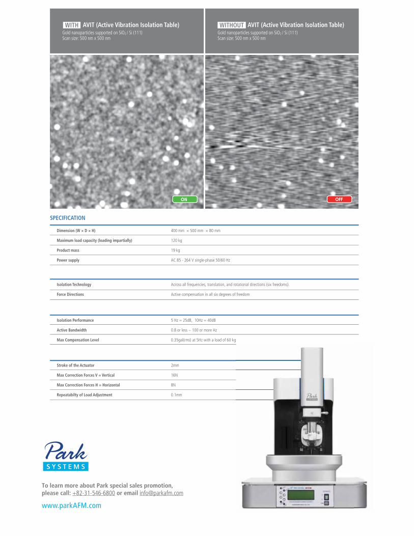
The effect of non-resonant vibration isolation produced via 6DOF active control results in outstanding performance over the all frequency range.
Automatic leveling & Clamping
You can activate automatic leveling and automatic clamping for transport with the push of a button.
Clean room-compatible
An aluminum surface plate and body eliminate the possibility of air contamination, and also it requires no air supply.
LCD monitor (standard equipment)AccelerogramAcceleration response spectrum
HEADQUARTERS
GLOBAL HEADQUARTERS +82-31-546-6800 AMERICAS HEADQUARTERS +1-408-986-1110
JAPAN HEADQUARTERS +81-3-3219-1001 SE ASIA HEADQUARTERS +65-6634-7470
Mini 450
www.parkAFM.com
To learn more about Park special sales promotion,please call: +82-31-546-6800 or email [email protected]
Dimension (W × D × H)
Maximum load capacity (loading impartially)
Product mass
Power supply
400 mm × 500 mm × 80 mm
120 kg
19 kg
AC 85 - 264 V single-phase 50/60 Hz
ON OFF
SPECIFICATION
AVIT (Active Vibration Isolation Table) Gold nanoparticles supported on SiO2 / Si (111)Scan size: 500 nm x 500 nm
AVIT (Active Vibration Isolation Table) Gold nanoparticles supported on SiO2 / Si (111)Scan size: 500 nm x 500 nm
WITH WITHOUT
Isolation Technology
Force Directions
Across all frequencies, translation, and rotational directions (six freedoms).
Active compensation in all six degrees of freedom
Isolation Performance
Active Bandwidth
Max Compensation Level
5 Hz = 25dB, 10Hz = 40dB
0.8 or less ~ 100 or more Hz
0.35gal(rms) at 5Hz with a load of 60 kg
Stroke of the Actuator
Max Correction Forces V = Vertical
Max Correction Forces H = Horizontal
Repeatabilty of Load Adjustment
2mm
16N
8N
0.1mm
The Most Accurate Atomic Force Microscope
Park NX10The quickest path to innovative research
www.parkAFM.com
NX10130822E16B
Park Systems Dedicated to producing the most accurate and easiest to use AFMs
www.parkAFM.com
More than a quarter century ago, the foundations for Park Systems were laid at Stanford University where Dr. Sang-Il Park, the founder of Park Systems worked as an integral part of the group that first developed AFM technology. After perfecting the technology, he then went on to create the first commercial AFM and later Park Systems was born.
Park Systems strives everyday to live up to the innovative spirit of its beginnings. Throughout our long history, we have honored our commitment to providing the most accurate and yet very easy to use AFMs, with revolutionary features like True Non-Contact™ mode, and many automated software. We are not simply content to rest on our past success. All of our products are designed with same care and creativity that went into our first, allowing you to focus on getting results without worrying about the integrity of your tools.
EUROPE
OCEANIA
France +33-1-6953-8023
Germany +49-6103-30098-0
Italy +39-02-9009-3082
Israel +972-3-923-9666
Switzerland +41-34-423-7070
Romania +40(0)-724-157-480
Spain and Portugal +34-902-244-343
Turkey +90-312-236-42-0708
UK an Ireland +44(0)1372-378-822
Benelux, Scandinavia, and Baltics +31-184-64-0000
Australia and New Zealand +61-2-9319-0122
HEADQUARTERS ASIAGLOBAL HEADQUARTERS +82-31-546-6800
AMERICAS HEADQUARTERS +1-408-986-1110
JAPAN HEADQUARTERS +81-3-3219-1001
SE ASIA HEADQUARTERS +65-6634-7470
AMERICAS USA: +1-408-986-1110
Canada: +1-888-641-0209
Brazil +55-11-4178-7070
China +852-2751-9488
India +91-40-2404-2353
Indonesia +62-21-384-6464
Malaysia +60-3-8075-2268
Philippines +632-807-2712
Saudi Arabia +966-2-640-5846
Taiwan +886-2-2755-2266
Thailand +662-668-2436
UAE +971-4-339-2603
Vietnam +844-3556-7371
The global headquarters is located at
Korean Advanced Nanotechnology Center (KANC) in Suwon, Korea.
The global headquarters is located at
Korean Advanced Nanotechnology Center (KANC) in Suwon, Korea.
Cell Discovery like Never BeforeIn-Liquid Biological Imaging with Park SICM
Human Foreskin Fibroblast COS M6 2F3 Cell Prostate Cell
Fibroblast Prostate Cell
C2C12 Bone Cancer Cell
Human Fetal Lung Fibroblast Hela Cell to Cell Connection
Rat Trachea HEp2 Cellular Surface
Cornea Collagen Film Rat Tail Collagen Network
COS (fibroblast-like cell) Pig Skin
Normal Rat Kidney Epithelial Skin Collagen Film Network
Madin-Darby Canin Kidney Benign Prostatic Hyperplasia
A6 Cell HaCaT (Cell Fusion) Large Instestine Tissue AGS cellHEK 293 3Y1 Rat Fibroblast (GFP)
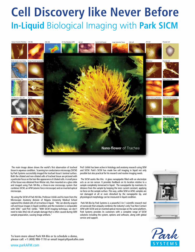
Nano-flower of Trachea
The main image above shows the world’s first observation of tracheal tissue in aqueous condition. Scanning ion conductance microscopy (SICM) by Park Systems successfully imaged the trachael tissue’s luminal surface. Both the ciliated and non-ciliated cells of tracheal tissue are pictured with a particular focus on the hair-like appearance of ciliated cells. A small piece of the tissue was obtained from Wistar rats, then mounted on a glass slide and imaged using Park NX-Bio, a three-in-one microscopy system that combines SICM, an AFM (atomic force microscope) and an inverted optical microscope.
By using the SICM of Park NX-Bio, Professor Ushiki and his team from the Microscopic Anatomy division of Niigata University Medical School captured the ciliated cells of rat trachea in liquid. "We can directly acquire cell and tissue images in liquid condition and the resolution is comparable with SEM," said Prof. Ushiki. "With SICM imaging technique, we don't need to take [the] risk of sample damage that is often caused during SEM sample preparation, causing image artifacts."
Prof. Ushiki has been active in histology and anatomy research using SEM and SICM. Park’s SICM has made live cell imaging in liquid not only possible but also practical for his research and routine imaging needs.
The SICM works like this: A glass nanopipette filled with an electrolyte acts as an ion sensor. It provides feedback on its location relative to a sample completely immersed in liquid. The nanopipette tip maintains its distance from the sample by keeping the ionic current constant, applying no force on the sample surface. This way, unlike SEM or AFM, samples are not damaged at all or even disturbed by the nanopipette tip, and physiological morphology can be measured in liquid condition.
Park NX-Bio by Park Systems is a powerful 3-in-1 scientific research tool at nanoscale that uniquely combines the industry’s only True Non-Contact AFM with SICM and an inverted optical microscope on the same platform. Park Systems provides its customers with a complete range of SICM solutions including the system, options and software, along with global service and support.
To learn more about Park NX-Bio or to schedule a demo,please call: +1 (408) 986-1110 or email [email protected]
www.parkAFM.com