anti-counterfeit nanoscale fingerprints based on randomly ...time.kaist.ac.kr/pub/101.pdf ·...
TRANSCRIPT
Nanotechnology
Nanotechnology 25 (2014) 155303 (7pp) doi:10.1088/0957-4484/25/15/155303
Anti-counterfeit nanoscale fingerprintsbased on randomly distributed nanowiresJangbae Kim1, Je Moon Yun1, Jongwook Jung1, Hyunjoon Song1,2,Jin-Baek Kim1 and Hyotcherl Ihee1,2
1 Department of Chemistry, Korea Advanced Institute of Science and Technology (KAIST),Daejeon 305-701, Republic of Korea2 Center for Nanomaterials and Chemical Reactions, Institute for Basic Science (IBS),Daejeon 305-701, Republic of Korea
E-mail: [email protected]
Received 21 December 2013, revised 29 January 2014Accepted for publication 13 February 2014Published 20 March 2014
AbstractCounterfeiting is conducted in almost every industry, and the losses caused by it aregrowing as today’s world trade continues to increase. In an attempt to provide an efficientmethod to fight such counterfeiting, we herein demonstrate anti-counterfeit nanoscalefingerprints generated by randomly distributed nanowires. Specifically, we prepare silvernanowires coated with fluorescent dyes and cast them onto the surface of transparent PETfilm. The resulting non-repeatable patterns characterized by the random location of thenanowires and their fluorescent colors provide unique barcodes suitable foranti-counterfeit purposes. Counterfeiting such a fingerprint pattern is impractical andexpensive; the cost of replicating it would be higher than the value of the typical targetitem being protected. Fingerprint patterns can be visually authenticated in a simple andstraightforward manner by using an optical microscope. The concept of generating uniquepatterns by randomness is not limited to the materials shown in this paper and should bereadily applicable to other types of materials.
Keywords: anti-counterfeit, fingerprint, fluorescence, nanowire, randomness
S Online supplementary data available from stacks.iop.org/Nano/25/155303/mmedia
1. Introduction
Counterfeiting is a steadily increasing and important problemthat affects all types of commercialized production. Accordingto the World Customs Organization, ∼6% of global goodstraded are counterfeit. The sale of counterfeit goods occurs innearly every trade and industry affecting our daily life becauseof globalization and the growth of internet trade. In manycases, it is very difficult to distinguish counterfeit goods fromgenuine products. Ironically, to some extent, customer demandencourages the counterfeiting business.
To date, there have been numerous attempts at anti-counterfeiting, including holography [1–3], laser surfaceauthentication (LSATM) [4], radio frequency identification(RFID) [5], nano barcodes [6, 7], surface enhanced Raman
scattering (SERS) and quantum dot tags [8, 9], and nanocom-posite tags [10]. In this paper, we propose a new approachbased on fingerprint patterns generated by randomly dis-tributed nanorods. Our key idea is that a unique pattern isgenerated simply by casting a handful of nanorods onto a plate.Because of naturally occurring randomness, the probability ofobtaining identical patterns is practically zero. Therefore,each pattern generated by simple casting is unique, likea fingerprint, and can thus be used as a security code orbarcode. If we expand this concept further, we can find somenano or subnano (or even micro and above) scale defectson the surfaces of many products, such as paper documents,whose defect profiles can also be recorded as unique barcodes.However, it would be more beneficial to create unique patternson the location selected for identification. For this purpose,
0957-4484/14/155303+07$33.00 1 c© 2014 IOP Publishing Ltd Printed in the UK
Nanotechnology 25 (2014) 155303 J Kim et al
we prepared a fingerprint pattern on a transferable film,specifically a flexible polyethylene terephthalate (PET) film,on which direction and target markers were patterned by aphotolithographic technique to provide positional informationfor identification. The target marker has a specified observationregion in which a hidden fingerprint pattern is prepared usingrandomly distributed silver nanowires (AgNWs). A simple,low-magnification optical microscope can be used to verifythe fingerprint pattern. The complexity of the pattern can befurther increased by coating the surfaces of the AgNWs withfluorescent dyes of various colors (red and green in this work);in this case, verification can be achieved by a fluorescencemicroscope. This fingerprint patterning technique is easilytransferable to any surface and provides artificial fingerprintsas nanoscale stamps. The authenticity verification is simple andstraightforward, allowing customers to immediately determinewhether products are authentic. Our technique is sufficientlysimple that anyone can prepare fingerprint patterns that cannotbe reproduced as a result of the underlying basic principleof randomness. This naturally occurring event enabled us toprepare novel fingerprint labels that can be used to combatpotential counterfeiting attempts.
2. Materials and methods
2.1. Synthesis of AgNWs
A 3.0 ml solution of PVP (0.6 M, M.W. 55 000, Sigma-Aldrich,Missouri, USA) and a 3.0 ml solution of AgNO3 (0.10 M,99.999%, Sigma-Aldrich, Missouri, USA) in ethylene glycol(Sigma-Aldrich, Missouri, USA) were alternately added to5.0 ml of boiling ethylene glycol every 30 s over a 7.5 minperiod. The resulting mixture was refluxed at ∼160 ◦C for1 h. The final solution was cooled, and the small particleswere removed by centrifugation at 1500 rpm for 10 min. Theproduct was purified by repetitive dispersion and precipitationcycles with ethanol (Junsei, Japan) to remove excess PVP andthen dispersed in ethanol (40 ml).
2.2. Silica coating of the AgNWs
A total of 0.350 ml of aqueous 30 vol.% NH4OH (Junsei,Japan) was mixed with 9.09 ml of isopropyl alcohol (Junsei,Japan), and 0.11 ml of tetraethyl orthosilicate (TEOS) (Sigma-Aldrich, Missouri, USA) was mixed with 7.9 ml of isopropylalcohol. A total of 2.00 ml of DI-H2O was first added to 5.0 mlof the AgNW dispersion, followed by the dropwise additionof the isopropyl alcohol solution of NH4OH. After 30 s, theisopropyl alcohol solution of TEOS was added to the finalAgNW dispersion. The final solution was stirred for 40 min toform silica-coated AgNWs.
2.3. FITC- or RITC-doped silica coating of the AgNWs
FITC (fluorescein isothiocyanate, Sigma-Aldrich, Missouri,USA) and RITC (rhodamine B-isothiocyanate, Sigma-Aldrich,Missouri, USA) were covalently linked to 3-aminopropyltrimethoxysilane (APTMS, TCI, Japan) by dissolving 100 mgof FITC in 186 µl of APTMS and 100 mg of RITC in 135 µl
of APTMS. Then, ethanol was added to make a 10 vol.%dye-linked APTMS in ethanol solution. The ethanol solutionof dye-linked APTMS was stirred for 24 h in the dark prior touse. The silica-coated AgNW dispersion (1 ml) was addeddropwise to 0.4 ml of isopropyl alcohol under vigorousstirring, followed by the addition of 0.1 ml DI-H2O. Separately,0.126 ml of the NH4OH was mixed with 9.62 ml of isopropylalcohol, and 0.1 ml of ethanol solution of the dye-linkedAPTMS was mixed with 9.9 ml of isopropyl alcohol. Next,0.72 ml of the isopropyl alcohol solution of NH4OH wasadded dropwise to the AgNW dispersion. After 30 s, 0.2 ml ofthe alcoholic solution of dye-linked APTMS was added to theAgNW dispersion. The final solution was stirred for 24 h.
2.4. Preparation of the photolithographic pattern on PET
A PET film was cut into strips 3 cm× 3 cm in size. ThePET strips were ultrasonically cleaned for 5 min in ace-tone, followed by chloroform. A negative-tone SU-8 2000.5(0.25 mg ml−1, MicroChem Corp., Massachusetts, USA)photoresist incorporating fluorescent dye (RB) was droppedonto the cleaned PET strips. The initial spin was set at 500 rpmfor a period of 10 s to spread the photoresist over the entiresample surface and then at 2000 rpm for 50 s. The coatedsamples were then soft baked on a hotplate at 95 ◦C for90 s to remove organic solvent. After the baking process, toprepare direction and target marker pattern arrays, the sampleswere exposed to UV light through a photomask with theappropriate design features for 45 s using a collimated UVsource (13.1 mW cm−2, MDA-6000DUV, MAIDAS SystemCo, Korea). A post-exposure baking process was performedon a hotplate at 95 ◦C for 5 min. Afterward, the samples weredeveloped in SU-8 developer for 60 s, rinsed with 2-propanol,and dried in a stream of nitrogen.
2.5. Preparation of the fingerprint pattern on PET
The preparation of the fingerprint pattern simply involvedalternately dropping a predetermined amount of FITC- orRITC-coated AgNW dispersion onto the target marker. Alter-natively, the dye-coated AgNW dispersion was premixedin any ratio, and this solution was dropped onto the targetmarker. Simply increasing the amount of solution droppedcould increase the number density of dye-coated AgNWsin the observation region. In addition, various mixing ratiosbetween the two colors of the dye-coated AgNW dispersioncould generate numerous different subset patterns. Practically,1 µl of solution was more than sufficient for the preparationof five or six fingerprint patterns.
2.6. Fluorescence microscopy
The optical and fluorescence images of the dye-labeled finger-printing patterns were observed using an inverted fluorescencemicroscope (IX71, Olympus) equipped with filter set typesU-MWB2 (460–490 nm excitation and 500 nm dichromaticmirror) and U-MWG2 (510–550 nm excitation and 570 nmdichromatic mirror). Direct visualization of the fingerprintingpattern was achieved via excitation of the FITC/RITC-labeled
2
Nanotechnology 25 (2014) 155303 J Kim et al
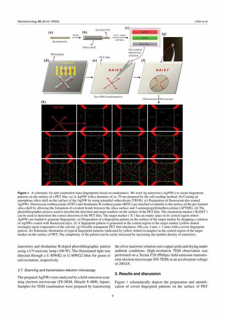
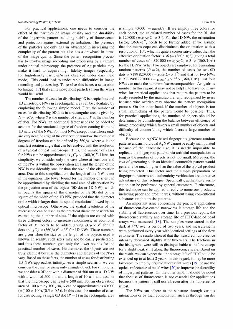
Figure 1. A schematic for anti-counterfeit nano-fingerprints based on randomness. We used Ag nanowires (AgNWs) to create fingerprintpatterns on the surface of a PET film. (a) A AgNW with a diameter of ca. 70 nm prepared by the self-seeding method. (b) Coating anamorphous silica shell on the surface of the AgNW by using tetraethyl orthosilicate (TEOS). (c) Preparation of fluorescent-dye-coatedAgNWs. Fluorescein isothiocyanate (FITC) and rhodamine B-isothiocyanate (RITC) are attached covalently to the surface of the pre-formedsilica shell by allowing the formation of covalent bonds between the silica surface and 3-aminopropyltrimethoxysilane (APTMS). (d) Thephotolithographic process used to inscribe the direction and target markers on the surface of the PET film. The orientation marker (‘KAIST’)can be used to determine the correct direction of the PET film. The target marker (‘X’) has an empty space in its central region whereAgNWs are loaded to generate fingerprints. (e) Preparation of a fingerprint pattern on the surface of the target marker by dropping a solutionof AgNWs coated with fluorescent dyes. (f) A fingerprint pattern is generated in the central region of the target marker (yellow dottedrectangle) upon evaporation of the solvent. (g) Flexible transparent PET film (thickness 100 µm, 5 mm × 5 mm) with a covert fingerprintpattern. (h) Schematic illustration of typical fingerprint patterns (indicated by yellow dotted rectangles) in the central region of the targetmarker on the surface of PET. The complexity of the pattern can be easily increased by increasing the number density of nanowires.
nanowires and rhodamine B-doped photolithographic patternusing a UV-mercury lamp (100 W). The illuminated light wasdirected through a U-MWB2 or U-MWG2 filter for green orred excitation, respectively.
2.7. Scanning and transmission electron microscopy
The prepared AgNWs were analyzed by a field-emission scan-ning electron microscope (FE-SEM, Hitachi S-4800, Japan).Samples for TEM examination were prepared by transferring
the silver nanowire solution onto copper grids and drying underambient conditions. High-resolution TEM observation wasperformed on a Tecnai F20 (Philips) field-emission transmis-sion electron microscope (FE-TEM) at an acceleration voltageof 200 kV.
3. Results and discussion
Figure 1 schematically depicts the preparation and identifi-cation of covert fingerprint patterns on the surface of PET
3
Nanotechnology 25 (2014) 155303 J Kim et al
film. AgNWs were chosen as the basic materials for randompatterns because (1) they can be easily observed by opticalor fluorescence microscopy, (2) their anisotropic well-defined1D structure is suitable for generating unique patterns, and(3) they can be prepared routinely in high volume by afacile process [11–13]. In principle, however, any NW ornanoscale (or even any) object can be used (figure 1(a)). Weprepared AgNWs via the self-seeding process according tothe literature [12, 13]. The resulting AgNWs had an averagelength of 10–50 µm and an average diameter of 70 ± 6 nm(figure S1 available at stacks.iop.org/Nano/25/155303/mmedia). The AgNW dispersion in ethanol usually contains a smallamount of nanoparticles, even after centrifugation. Althoughthey make the overall pattern appear noisier, these nanoparti-cles actually increase the complexity of the pattern.
While the AgNW-based random patterns alone servedour purpose, we added complexity by coloring the AgNWswith various fluorescent dyes so that the hidden color infor-mation could be detected only via fluorescent detection. Toachieve this goal, we formed amorphous silica shells onthe surfaces of the as-synthesized AgNWs by employinga previously reported method [14, 15]. The prepared sil-ica layer was further reacted with fluorescent dyes (fluo-rescein isothiocyanate, FITC; rhodamine B-isothiocyanate,RITC) linked to 3-aminopropyltrimethoxysilane (APTMS) toprepare dye-coated AgNWs by allowing the formation ofcovalent bonds between the silica surface and the APTMS(figures 1(b) and (c)). The silica layer not only provides thesurface chemistry necessary to attach fluorescent dyes to itssurface covalently but also enhances visibility by increasingthe thickness of the AgNW (ca. 212 nm). Considering theresolution limit of the optical microscope, thickness increaseis highly preferable. With green light (550 nm), the estimatedoptical resolution limit is approximately 350 nm. In practice,the lowest value obtainable with conventional lenses is approx-imately 200 nm [16]. Note that fluorescent dyes should beattached to the surface of a pre-formed silica shell to avoid thedissolution of core AgNWs, which occurs if the silica coatingand fluorescent dye coating are performed simultaneously. Asmall portion of AgNWs were found to remain intact, evenafter the fluorescent dye molecules were conjugated to thesilica layer. These non-fluorescent AgNWs were also usedas basic components for generating the fingerprint patternbecause they could not be removed from the fluorescent AgNWmixture. The randomly distributed fingerprint pattern becameincreasingly complex as a result of the existence of non-fluorescent AgNWs because all optically active AgNWs underbright field observation do not contribute to the fluorescentimages.
A flexible transparent PET film was used as the substrateon which a rhodamine B (RB) dye-incorporated photoresist(SU-8 2000.5) pattern was prepared by a conventional pho-tolithographic technique using an I-Line UV (figure 1(d)).After the photolithographic processes had been performed,the orientation marker (‘KAIST’) and the target marker (‘X’)were prepared on the surface of the flexible PET film. Thethickness of the prepared markers was measured to be ca.600 nm from the flat surface. The orientation marker indicates
the correct observation direction for the flexible PET film.That is, the correct orientation of the PET film is defined as thedirectional placement in which we can read the label ‘KAIST’correctly (figure S2 available at stacks.iop.org/Nano/25/155303/mmedia). The target marker (‘X’) in the center of the PETfilm indicates the location of the observation region, whichhas dimensions of 100 µm× 100 µm (figure 1(e)), where therandomly distributed fluorescent-dye-coated AgNWs are cast,and thereafter the fingerprint patterns can be observed usingan optical or fluorescence microscope. Because the letter ‘X’has dimensions of 800 µm× 700 µm, with a line width of20 µm and a height of ca. 600 nm, the existence of preparedpatterns can be identified even by the naked eye. Once wehave confirmed the ideal position of the substrate using theorientation marker, the target marker can be easily observedby moving down from the orientation marker by 590 µm, andthe observation region can consequently be readily identifiedby following the lines of the ‘X’.
The fingerprint patterns are prepared by dropping apredetermined amount of AgNW dispersion on the targetmarker on the surface of the PET film, followed by air drying(figure 1(e)). Upon solvent evaporation, a random distributionof the dye-coated AgNWs on the film occurs, thereby leadingto the formation of a unique fingerprint pattern (figure 1(f)).Notably, a flexible transparent PET film with a thickness of100 µm presents advantages with respect to application andprocessing. One of the greatest advantages of such a PET filmis that it can be cut to any size and shape and attached tovarious surfaces via simple treatments (figure 1(g)).
The prepared fingerprint pattern can be easily observedby using an optical/fluorescence microscope, as representedschematically in figure 1(h). As mentioned previously, we canidentify the correct orientation using the orientation marker(‘KAIST’), which in turn allows us to easily find the targetmarker (‘X’). Based on magnified (1000×) images focusingon the observation region in the center of the target marker(yellow dotted square), the fingerprint pattern can be readilyidentified. Thereafter, these observed fingerprint images can bestored in a database with intrinsic ID numbers for authenticityverification. The number of AgNWs distributed in the obser-vation region can be easily controlled by the concentration offluorescent AgNWs. Various schematic fingerprint patternsare represented by the number density of nanowires andthe distribution patterns in figure 1(h). Considering the largenumber of cases that can be generated by distributing a singleAgNW in a square measuring 100 µm× 100 µm, several tensof AgNWs can generate a nearly infinite number of uniquedistribution patterns, for which the probability of obtainingtwo identical patterns is practically zero.
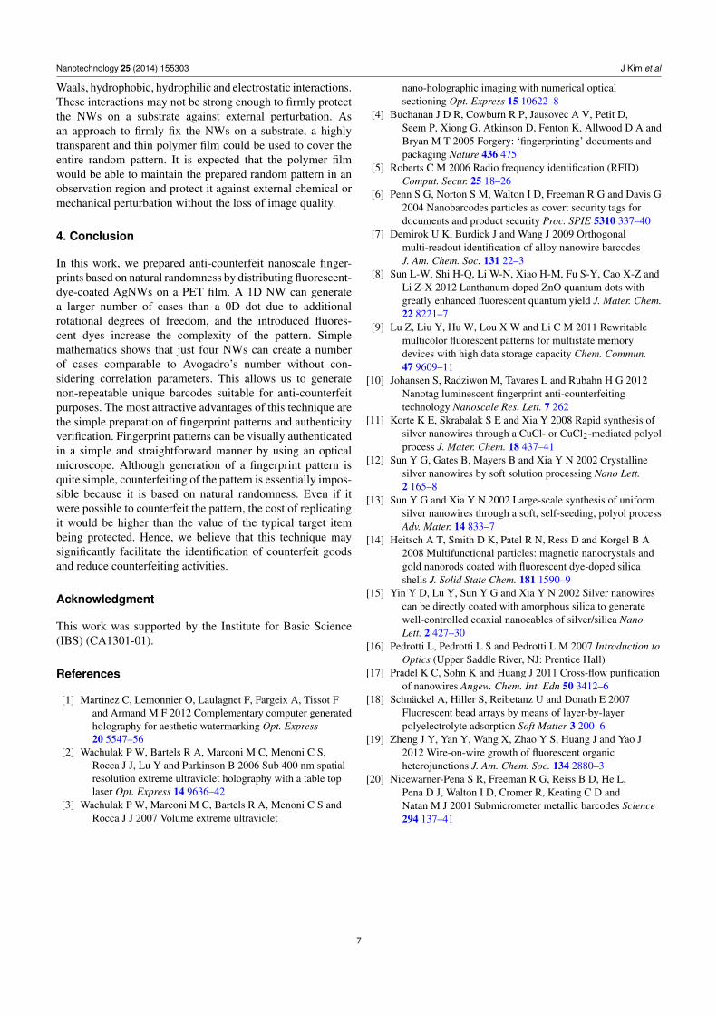
We prepared many fingerprints on the surface of PETfilm and selected 12 sets for clear visualization, as shownin figure 2. Figure 2(c) represents the fingerprint patternswith enhanced visibility that were created by employingfluorescent-dye-coated AgNWs with an average diameter ofca. 392 nm, which is 1.8 times thicker than the AgNWs infigures 2(a) and (b). All of the observed images from the PETfilm (figure 2) show distinct, randomly distributed patterns,and no identical images can be found. Here, three major factors
4

Nanotechnology 25 (2014) 155303 J Kim et al
Figure 2. A series of fingerprint patterns with various number densities of dye-coated AgNWs. A series of bright field optical (left) andfluorescence (right) images are displayed with target markers (black dotted parallelograms) and central fingerprint regions (yellow dottedrectangles; 100 µm× 100 µm) for better visualization for three number densities of AgNWs: (a) low, (b) medium and (c) high. Thefluorescence images are prepared by combining individual red and green fluorescence images that are detected from the same viewpoint andfield of interest. The scale bar shown in the first figure is common for all figures. The average diameters of the AgNWs are ca. 200 nm, ca.212 nm, and 392 nm for (a), (b), and (c), respectively.
govern the generation of fingerprints: (1) the lack of AgNWswith identical lengths in the observation region, (2) nearlyinfinite spatial (position and orientation) degrees of freedomgenerated by multiple AgNWs inside the observation region,and (3) varied mixing ratios between the two different colors aswell as fluorescently inactive objects. Thus, the combination ofthese factors makes the number of cases for potential randompatterns practically infinite. Furthermore, the nanoparticlesthat remain in the AgNW dispersion also contribute to thecomplexity of the fingerprint pattern (figure 2).
As a final step, a unique ID (barcode) can be assigned toeach unique fingerprint; this ID can facilitate a quick search in adatabase. The authentication process would be the same as the
pattern observation process using a microscope (figure 1(h)). Ifthe substrate is positioned in the correct orientation, the brightfield and fluorescence images of the observation region canbe displayed and visually compared with the stored images.Comparison of both bright field and fluorescent images willminimize the occurrence of authentication failures as a resultof non-fluorescent AgNWs. These authentication processescan be automated by employing an algorithm that recognizesthe positions and colors of the AgNWs and digitizing thatinformation in a database. Such digitized information couldsignificantly reduce the size of the stored data and reduce thetime required for the authentication process.
5
Nanotechnology 25 (2014) 155303 J Kim et al
For practical applications, one needs to consider theeffect of the particles on image quality and the durabilityof the fingerprint pattern including stability of fluorescenceand protection against external perturbation. The presenceof the particles not only has an advantage in increasing thecomplexity of the pattern but also has a drawback in termsof the image quality. Since the pattern recognition processhas to involve image recording and processing by a cameraunder optical microscopy, the presence of Ag particles maymake it hard to acquire high fidelity images (especiallyfor high-density particles/wires observed under dark fieldmode). This could lead to undesirable difficulties in imagerecording and processing. To resolve this issue, a separationtechnique [17] that can remove most particles from the wireswould be useful.
The number of cases for distributing 0D isotropic dots and1D anisotropic NWs in a rectangular area can be calculated byemploying the following simple model. First, the number ofcases for distributing 0D dots in a rectangular area is given byN = SCP , where S is the number of sites and P is the numberof dots. For NWs, an additional factor needs to be added toaccount for the rotational degree of freedom coming from the1D nature of the NWs. For most NWs except those whose endsare very near the edge of the observation window, the rotationaldegrees of freedom can be defined by 360/n, where n is thesmallest rotation angle that can be resolved with the resolutionof a typical optical microscope. Thus, the number of casesfor NWs can be approximated as SCP × (360/n)P . Here, forsimplicity, we consider only the case where at least one endof the NW is within the observation area and the length of theNW is considerably smaller than the size of the observationarea. Due to this simplification, the length of the NW is notin the equation. The lower bound for the number of sites canbe approximated by dividing the total area of observation bythe projection area of the object (0D dot or 1D NW), whichis roughly the square of the diameter of the 0D dot or thesquare of the width of the 1D NW, provided that the diameteror the width is larger than the spatial resolution allowed by theoptical microscope. Otherwise, the spatial resolution of themicroscope can be used as the practical diameter or width forestimating the number of sites. If the objects are coated withthree different colors to increase randomness, an additionalfactor of 3P needs to be added, giving SCP × 3P for 0Ddots and SCP × (360/n)P
× 3P for 1D NWs. These numbersare given when the size or the length of the objects used isknown. In reality, such sizes may not be easily predictable,and thus these numbers give only the lower bounds for thepractical number of cases. Furthermore, the objects are nottruly identical because the diameters and lengths of the NWsvary. Based on these facts, the number of cases for distributing1D NWs approaches infinity. As a simple scenario, we canconsider the case for using only a single object. For simplicity,we consider a 0D dot with a diameter of 500 nm or a 1D NWwith a width of 500 nm and a length of 10 µm and assumethat the microscope can resolve 500 nm. For an observationarea of 100 µm by 100 µm, S can be approximated as 40 000(=(100× 100)/(0.5× 0.5)). In this case, the number of casesfor distributing a single 0D dot (P = 1) in the rectangular area
is simply 40 000 (= 40 000C1). If we employ three colors foreach object, the calculated number of cases for the 0D dotis 120 000 (= 40 000C1× 31). For the 1D NW, the orientationfactor, (360/n)P , needs to be further added. If we assumethat the microscope can discriminate the orientation with aresolution of 10◦, which is quite a conservative value, then theeffective orientation factor is 36 (= (360/10)1), giving a totalnumber of cases of 4 320 000 (= 40 000C1 × 31
× (360/10)1)for the 1D NW. When two objects are employed for generatingrandom patterns (P = 2), the number of cases for two 0Ddots is 7199 820 000 (= 40 000C2× 32) and that for two NWsis 9330 966 720 000 (= 40 000C2× 32
× (360/10)2). Just fourNWs can make the number of cases comparable to Avogadro’snumber. In this regard, it may not be helpful to have too manywires for practical applications that require the pattern to beeasily recorded by the manufacturer and recognized by usersbecause wire overlap may obscure the pattern recognitionprocess. On the other hand, if the number of objects is toosmall, mimicking of the pattern would be possible. Thus,for practical applications, the number of objects should bedetermined by considering the balance between efficiency ofimage processing which favors a small number of objects anddifficulty of counterfeiting which favors a large number ofobjects.
Because the AgNW-based fingerprints generate randompatterns and an individual AgNW cannot be easily manipulatedbecause of the nanoscale size, it is nearly impossible toreplicate the fingerprint patterns via artificial manipulation aslong as the number of objects is not too small. Moreover, thecost of generating such an identical counterfeit pattern wouldgenerally be much higher than the value of the typical productbeing protected. This factor and the simple preparation offingerprint patterns and authenticity verification are attractiveadvantages of this technique. Specifically, authenticity verifi-cation can be performed by general customers. Furthermore,this technique can be applied directly to numerous products,including paper and credit cards, without using conventionalsubstrates or photoresist patterns.
An important issue concerning the practical applicationof fluorescent-dye-coated nanowires is storage life and thestability of fluorescence over time. In a previous report, thefluorescence stability and storage life of FITC-labeled beadarrays was measured [18]. The samples were stored in thedark at 4 ◦C over a period of two years, and measurementswere performed every year with identical settings of the flowcytometer. The results showed that the measured fluorescenceintensity decreased slightly after two years. The fractions inthe histograms were still as distinguishable as before exceptfor a slight peak shift along the fluorescence scale. Based onthe result, we can expect that the storage life of FITC could beextended up to at least 2 years. In this regard, it may be morefavorable to employ organic fluorescent wires [19] or use theoptical reflectance of metal wires [20] to improve the durabilityof fingerprint patterns. On the other hand, it should be notedthat the use of fluorescence is not essential for applicationsbecause the pattern is still useful, even after the fluorescenceis lost.
The NWs can adhere to the substrate through variousinteractions or by their combination, such as through van der
6
Nanotechnology 25 (2014) 155303 J Kim et al
Waals, hydrophobic, hydrophilic and electrostatic interactions.These interactions may not be strong enough to firmly protectthe NWs on a substrate against external perturbation. Asan approach to firmly fix the NWs on a substrate, a highlytransparent and thin polymer film could be used to cover theentire random pattern. It is expected that the polymer filmwould be able to maintain the prepared random pattern in anobservation region and protect it against external chemical ormechanical perturbation without the loss of image quality.
4. Conclusion
In this work, we prepared anti-counterfeit nanoscale finger-prints based on natural randomness by distributing fluorescent-dye-coated AgNWs on a PET film. A 1D NW can generatea larger number of cases than a 0D dot due to additionalrotational degrees of freedom, and the introduced fluores-cent dyes increase the complexity of the pattern. Simplemathematics shows that just four NWs can create a numberof cases comparable to Avogadro’s number without con-sidering correlation parameters. This allows us to generatenon-repeatable unique barcodes suitable for anti-counterfeitpurposes. The most attractive advantages of this technique arethe simple preparation of fingerprint patterns and authenticityverification. Fingerprint patterns can be visually authenticatedin a simple and straightforward manner by using an opticalmicroscope. Although generation of a fingerprint pattern isquite simple, counterfeiting of the pattern is essentially impos-sible because it is based on natural randomness. Even if itwere possible to counterfeit the pattern, the cost of replicatingit would be higher than the value of the typical target itembeing protected. Hence, we believe that this technique maysignificantly facilitate the identification of counterfeit goodsand reduce counterfeiting activities.
Acknowledgment
This work was supported by the Institute for Basic Science(IBS) (CA1301-01).
References
[1] Martinez C, Lemonnier O, Laulagnet F, Fargeix A, Tissot Fand Armand M F 2012 Complementary computer generatedholography for aesthetic watermarking Opt. Express20 5547–56
[2] Wachulak P W, Bartels R A, Marconi M C, Menoni C S,Rocca J J, Lu Y and Parkinson B 2006 Sub 400 nm spatialresolution extreme ultraviolet holography with a table toplaser Opt. Express 14 9636–42
[3] Wachulak P W, Marconi M C, Bartels R A, Menoni C S andRocca J J 2007 Volume extreme ultraviolet
nano-holographic imaging with numerical opticalsectioning Opt. Express 15 10622–8
[4] Buchanan J D R, Cowburn R P, Jausovec A V, Petit D,Seem P, Xiong G, Atkinson D, Fenton K, Allwood D A andBryan M T 2005 Forgery: ‘fingerprinting’ documents andpackaging Nature 436 475
[5] Roberts C M 2006 Radio frequency identification (RFID)Comput. Secur. 25 18–26
[6] Penn S G, Norton S M, Walton I D, Freeman R G and Davis G2004 Nanobarcodes particles as covert security tags fordocuments and product security Proc. SPIE 5310 337–40
[7] Demirok U K, Burdick J and Wang J 2009 Orthogonalmulti-readout identification of alloy nanowire barcodesJ. Am. Chem. Soc. 131 22–3
[8] Sun L-W, Shi H-Q, Li W-N, Xiao H-M, Fu S-Y, Cao X-Z andLi Z-X 2012 Lanthanum-doped ZnO quantum dots withgreatly enhanced fluorescent quantum yield J. Mater. Chem.22 8221–7
[9] Lu Z, Liu Y, Hu W, Lou X W and Li C M 2011 Rewritablemulticolor fluorescent patterns for multistate memorydevices with high data storage capacity Chem. Commun.47 9609–11
[10] Johansen S, Radziwon M, Tavares L and Rubahn H G 2012Nanotag luminescent fingerprint anti-counterfeitingtechnology Nanoscale Res. Lett. 7 262
[11] Korte K E, Skrabalak S E and Xia Y 2008 Rapid synthesis ofsilver nanowires through a CuCl- or CuCl2-mediated polyolprocess J. Mater. Chem. 18 437–41
[12] Sun Y G, Gates B, Mayers B and Xia Y N 2002 Crystallinesilver nanowires by soft solution processing Nano Lett.2 165–8
[13] Sun Y G and Xia Y N 2002 Large-scale synthesis of uniformsilver nanowires through a soft, self-seeding, polyol processAdv. Mater. 14 833–7
[14] Heitsch A T, Smith D K, Patel R N, Ress D and Korgel B A2008 Multifunctional particles: magnetic nanocrystals andgold nanorods coated with fluorescent dye-doped silicashells J. Solid State Chem. 181 1590–9
[15] Yin Y D, Lu Y, Sun Y G and Xia Y N 2002 Silver nanowirescan be directly coated with amorphous silica to generatewell-controlled coaxial nanocables of silver/silica NanoLett. 2 427–30
[16] Pedrotti L, Pedrotti L S and Pedrotti L M 2007 Introduction toOptics (Upper Saddle River, NJ: Prentice Hall)
[17] Pradel K C, Sohn K and Huang J 2011 Cross-flow purificationof nanowires Angew. Chem. Int. Edn 50 3412–6
[18] Schnackel A, Hiller S, Reibetanz U and Donath E 2007Fluorescent bead arrays by means of layer-by-layerpolyelectrolyte adsorption Soft Matter 3 200–6
[19] Zheng J Y, Yan Y, Wang X, Zhao Y S, Huang J and Yao J2012 Wire-on-wire growth of fluorescent organicheterojunctions J. Am. Chem. Soc. 134 2880–3
[20] Nicewarner-Pena S R, Freeman R G, Reiss B D, He L,Pena D J, Walton I D, Cromer R, Keating C D andNatan M J 2001 Submicrometer metallic barcodes Science294 137–41
7