center for nanoscale science and technology – nist nanotechnology r&d at nist robert celotta,...
TRANSCRIPT
Center for Nanoscale Science and Technology – NIST
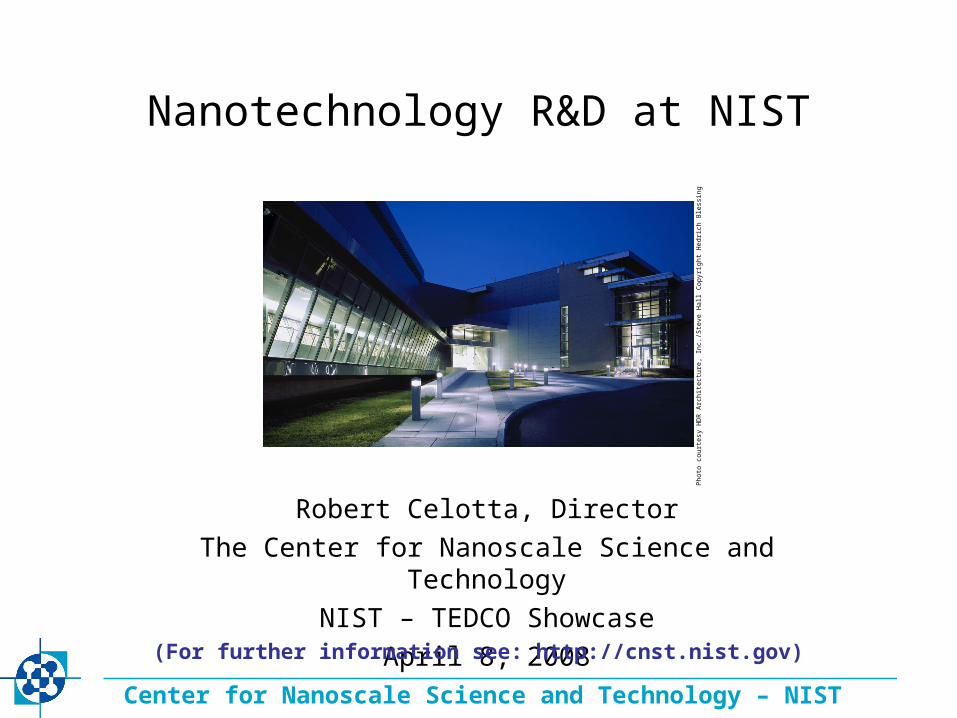
Nanotechnology R&D at NIST
Robert Celotta, Director
The Center for Nanoscale Science and Technology
NIST – TEDCO Showcase
April 8, 2008(For further information see: http://cnst.nist.gov)
Pho
to c
ourt
esy
HD
R A
rchi
tect
ure,
Inc
./S
teve
Hal
l Cop
yrig
ht H
edric
h B
less
ing

2
Center for Nanoscale Science and Technology – NIST
Outline
• NIST at a Glance• The New Center for Nanoscale Science and
Technology– The Nanofab– The Research Program
• Quick Tour of Nanotechnology throughout NIST
3
Center for Nanoscale Science and Technology – NIST
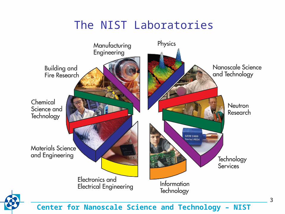
The NIST Laboratories
4
Center for Nanoscale Science and Technology – NIST
CNST Mission and Structure
Mission: • To enable the development of nanotechnology
– Provides both research and access to facilities– Works to solve outstanding nanoscale measurement and
fabrication problems
Structure:• The CNST consists of a Research Program and the
CNST Nanofab– The Nanofab
• A national facility offering convenient and economical access to expensive nanoscale measurement and fabrication tools.
– The Research Program• Multidisciplinary research staff operates in a highly collaborative
mode

5
Center for Nanoscale Science and Technology – NIST
Advanced Measurement Laboratory
• CNST leverages the facilities of the AML – arguably the world’s most advanced laboratory – for its nanotechnology research.
6
Center for Nanoscale Science and Technology – NIST
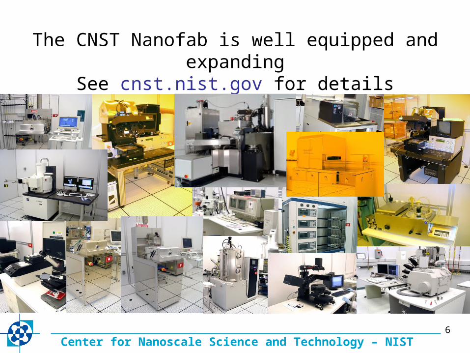
The CNST Nanofab is well equipped and expandingSee cnst.nist.gov for details

7
Center for Nanoscale Science and Technology – NIST
Research Program
Developing measurement capabilities for:– Future Electronics
• Devices, architectures, interconnects– Nanomanufacturing and Nanofabrication
• Top-down and bottom-up fabrication and assembly– Energy
• Conversion, storage, and transport• Complementary to and interactive with strong, existing NIST
Laboratory programs• Areas of concentration will, of necessity, change with needs

8
Center for Nanoscale Science and Technology – NIST
Core Competences• Atomic Scale Characterization and Manipulation
– Fabrication and measure the geometric and electronic structure of materials with atomic resolution using a UHV cryogenic/high magnetic field scanning tunneling microscope system.
• Directed Assembly– Fabrication and study the effects of templating structures on the organization of nanoscale materials and their resultant
properties.
• Laser-Atom Manipulation– Laser control of atomic motion is used to develop new nanofabrication and nanoscale measurement methods.
• Nanomagnetic Imaging (SEMPA)– Use of spin polarized electrons generated in a scanning electron microscope to image magnetic structures over a large
magnification range. Measurements are sensitive to less than a monolayer of magnetic material.
• Nanophotonics– Study of nanofabricated optical structures that confine light to wavelength-scale dimensions and to investigate light-matter
interactions with near-field probing and microphotoluminescence setups.
• Nanoscale Transport – Device fabrication and photo-electrical probing of electronic and ionic transport properties of thin-film materials and nanoscale
objects equipped with probe station, cryostats, air/ liquid /high-vacuum STM/cAFM.
• Nanoplasmonics – Design and nanofabrication of metal-based photonic components and metamaterials which exploit subwavelength confinement of
light, for applications in information processing, metrology, and microscopy.
• Nanomagnet Dynamics – Fabrication and measurement of magnetization dynamics of magnetic nanostructures. Microwave spectroscopy techniques yield
precise information on material and structure properties at the nanoscale
NEMs, MEMs, Nanoscale Process Control (Coming soon) +

9
Center for Nanoscale Science and Technology – NIST
Highlights:
• Molecular Spintronics– Used nanoscale pore in Si wafer
– One molecule thick layer of self assembled molecules
– Observed vibrational energies of molecular states
• Laser-based Nanotube Cleanup– Purifies raw nanotube material
– Reduces carbon impurities, e.g., graphite, soot, etc.
– Does not destroy tubes • Nanoscale Pores Provide Analysis
– Detects and sorts different sized polymer chains
– Uses a lipid bilayer membrane
– Pore size ~ 1.5 nm
– Current flow indicates chain size

10
Center for Nanoscale Science and Technology – NIST
Highlights:
• Nanotechnology Research Recognized with two Nano 50 Awards– Scanning Electron Microscopy
– Scatterfield Optical Microscopy
• First Results Reported for Helium Ion Microscopy– New instrument has been installed
– Study of imaging process has begun

11
Center for Nanoscale Science and Technology – NIST
Highlights:
• Nanowire Device Fabrication Method Demonstrated– Nanowires grown on sapphire wafer in specific locations and
directions
– Gold deposits used as nucleation points
– Zinc Oxide nanowires grown to create 600 nanowire based transistors
• Nanoelectronic Switch Demonstrated– Uses self-assembled layers of organic molecules
– Silver atoms quickly assemble to form conduction path
– Growth provides nanoscale binary switch
• SWNT Interaction with Polarized Light Studied– DNA stretching alignment method used
– First experimental verification of optical response
– Joint with Physics Lab and RIT

12
Center for Nanoscale Science and Technology – NIST
Highlights:
• New Hybrid Microscope Developed– Scanning Photoionization Microscopy (SPIM)– High spatial resolution – Electrical sensitivity from low energy electron detection
• Highly Charged Ions Used to Study GMR/TMR– Insulating buffer layer modified by xenon +44 ions– Device incorporates both GMR and TMR effects
• High Speed Nanoscale Vibrations Measured– The 40 MHz NEM vibrations observed– Offers potential of 500-fold increase in STM speed

13
Center for Nanoscale Science and Technology – NIST
Highlights:
• “Fossilized Liquid Assembly”– Components self assemble freely in liquid– UV light exposure polymerizes a monomer– Allows the study of the self assembly process
• Carbon Nanotube Tools– Carbon “nanoknife” stretched between two tungsten
needles– Could be applied to slice individual cells
• Rapid Method for Judging Nanotube Purity– Uses simple quartz crystal apparatus– Resonance frequency change on heating– Gauges consistency of samples

Center for Nanoscale Science and Technology – NIST
Nanotechnology R&D at NIST
Robert Celotta, Director
The Center for Nanoscale Science and Technology
NIST – TEDCO Showcase
April 8, 2008(For further information see: http://cnst.nist.gov)
Pho
to c
ourt
esy
HD
R A
rchi
tect
ure,
Inc
./S
teve
Hal
l Cop
yrig
ht H
edric
h B
less
ing

15
Center for Nanoscale Science and Technology – NIST
Using the CNST Nanofab
• The Nanofab is a nanofabrication and nanoscale measurement facility– Based on highly successful NNIN Nanocenter model– Fee based, shared use
• Open to all users– NIST site access restrictions apply
• Fees are based on operating costs– Similar to the full cost recovery fees of the NNIN-NSF Nanocenters
• External users may apply to have a portion of their fee waived– For research supportive of CNST goals– Net charges similar to NNIN-NSF “academic” rates
• The Nanofab will train users in tool use– Alternatively, the process can performed by a process engineer at an additional
cost• User can maintain IP rights under certain circumstances• For information about use of the Nanofab
– Contact Dr. Alex Liddle ([email protected]),