modeling and stability analysis of active/hybrid common
TRANSCRIPT
6254 IEEE TRANSACTIONS ON POWER ELECTRONICS, VOL. 31, NO. 9, SEPTEMBER 2016
Modeling and Stability Analysis of Active/HybridCommon-Mode EMI Filters for DC/DC
Power ConvertersYongbin Chu, Student Member, IEEE, Shuo Wang, Senior Member, IEEE, and Qinghai Wang
Abstract—Hybrid electromagnetic interference (EMI) filters(HEFs), which are composed of an active filter and a passive fil-ter, have been proposed to reduce the size and weight of conven-tional passive EMI filters in literatures. However, accurate modelsthat can be used to predict the stability and performance of HEFshave not been developed. To cope with this, this paper presents amodeling technique for a hybrid common-mode (CM) filter. Thetechnique can be applied to the modeling of other HEFs. Criticalcomponent models were first developed for the HEF. HEF’s overallmodel was further developed based on these individual compo-nent models. Experimental results validated that the developedmodel can successfully predict the stability and performance ofactive/hybrid CM filters.
Index Terms—Active EMI filters, CM noise, hybrid EMI filters,modeling, stability analysis.
I. INTRODUCTION
SWITCHED-MODE power supplies generate conductedelectromagnetic interference (EMI) noise due to their fast
switching of high currents and high voltages. Various elec-tromagnetic compatibility (EMC) standards [1]–[3] have beenapplied to both consumer and industry products. Generally,EMI noise includes differential-mode (DM) noise and common-mode (CM) noise. Passive EMI filters, which are composed ofinductors and capacitors, are widely used to suppress EMI noise.
As power electronics moves to high power density, EMI filtersare becoming one of the biggest function units in the powerconverters. For CM EMI filters, the maximum CM capacitanceis limited by the safety standards so CM inductors usually have abig inductance. Furthermore, the CM inductor windings conductfull power currents so the CM inductors are usually big [2], [4]and heavy [5].
A hybrid filter (HEF) is composed of an active filter anda passive filter. The active filter reduces low-frequency EMInoise and the passive filter reduces high-frequency EMI noise.Because the passive filter has a much higher corner frequency
Manuscript received July 30, 2015; revised October 10, 2015; acceptedNovember 3, 2015. Date of publication November 20, 2015; date of current ver-sion March 25, 2016. This work was supported by Huawei Innovation ResearchProgram. Recommended for publication by Associate Editor A. Lindemann.
Y. Chu is with Texas Instruments, Dallas, TX 75243 USA (e-mail:[email protected]).
S. Wang is with the Department of Electrical and Computer Engineering, Uni-versity of Florida, Gainesville, FL 32611 USA (e-mail: [email protected]).
Q. Wang is with Huawei Technologies, Co., Shenzhen 518129 China (e-mail:[email protected]).
Color versions of one or more of the figures in this paper are available onlineat http://ieeexplore.ieee.org.
Digital Object Identifier 10.1109/TPEL.2015.2502218
than a conventional EMI filter, the passive filter size is greatlyreduced. The total size and weight of the active and passivefilters could also be much smaller than a conventional passiveEMI filter [4], [6]. At the same time, the HEF could have a betterperformance than a conventional passive EMI filter because thepassive filter has a better high-frequency performance due to itssmaller parasitic parameters.
A considerable amount of research has been conducted onHEFs. Various HEFs have been implemented in dc/dc con-verters, motor drive systems, electric vehicles, etc. [3]–[24].LaWhite and Schlecht [7] discussed the use of active DM filtersin conjunction with minimal passive filters for a high switch-ing frequency converter. Farkas and Schlecht [8] discussed theviability of active EMI filters for utility applications. In [9],a circuit element, nullor, was used to describe the active ripplefilters and four basic circuit configurations for ripple current can-cellation was classified and compared. Son and Seung-Ki [10]conducted a generalized analysis of active EMI filter topologies.A current-sense current-compensation feedback hybrid EMI fil-ter had been designed for industry application in [11] and [12].Hybrid EMI filters used in motor drive systems were evaluatedand implemented in [4] and [13]–[17]. Recently, a digital activeEMI filter was proposed and applied to a microinverter moduleand a dc/dc converter [18], [19].
The insertion gain and stability for HEFs were discussed inseveral articles [1], [7], [20]–[22]. Chen et al. [20] evaluates theperformance of a hybrid CM filter through active impedancemultiplication method. In [21], the stability of a current-senseand voltage the feedback active EMI filter was discussed. How-ever, the effect of noise source impedance was missed and exper-imental validation was not provided. Guidelines on the designof a feed forward voltage-sense voltage-feedback CM HEF wasgiven in [22].
Different from the existing work above, this paper focuseson the development of a modeling technique for a hybrid CMfilter. The developed technique can be extended to other HEFs.It would be a good tool for HEF’s stability and performanceanalysis. A hybrid current-sense and current-feedback CM filteris introduced and analyzed in Section II. Critical componentmodels are developed in Section III. The overall model of thehybrid CM filter is further developed based on these individualcomponent models in Section IV. The model is used for stabilityanalysis and is validated by experimental results in Section V. InSection VI, the model is used to evaluate a HEF’s performance.It is shown that the developed model can successfully predictthe stability and performance of the hybrid CM filter.
0885-8993 © 2015 IEEE. Personal use is permitted, but republication/redistribution requires IEEE permission.See http://www.ieee.org/publications standards/publications/rights/index.html for more information.
Authorized licensed use limited to: University of Florida. Downloaded on December 30,2020 at 05:05:33 UTC from IEEE Xplore. Restrictions apply.

CHU et al.: MODELING AND STABILITY ANALYSIS OF ACTIVE/HYBRID CM EMI FILTERS FOR DC/DC POWER CONVERTERS 6255
Fig. 1. Hybrid CM filter under investigation.
II. HYBRID CM FILTER UNDER INVESTIGATION
Fig. 1 shows the hybrid CM filter under investigation. InFig. 1, the CM capacitors 2 × CY 1 , 2 × CY 2 , resistors 2 × RY 1 ,and the CM inductor L compose a passive CM filter. The fil-ter reduces the noise ripple and attenuates high-frequency CMnoise to ensure the hybrid CM filter works properly [4]. Theresistors 2 × RY 1 are used to damp resonant peaking of thepassive filter. CX 1 , CX 2 , and CX 3 are DM capacitors. A pairof line impedance stabilization networks (LISNs) is connectedbetween a dc source and the hybrid CM filter for conductiveEMI measurement.
The active part of the hybrid CM filter is mainly composed ofa current transformer (CT), an operational amplifier circuit, andan RC branch connected between the output of the operationalamplifier and the ground. The CT is a three winding CT usedfor CM noise current sensing. Its two primary windings areconnected to a converter’s main power paths. They have thesame number of turns and are directly coupled. The CM currentsin the main power paths of the converter will generate signals inthe third winding on the secondary side. On the other hand, theDM currents will not generate signals in the third winding on thesecondary side because the DM magnetic flux is canceled withinthe CT. R1 converts the sensed CM currents into voltages. Thevoltages are fed to an operational amplifier U1 . The noninvertinginput of U1 is connected to VEE through an ac capacitor (notshown here). The output of the amplifier is coupled throughRco and Cco to the ground. This capacitive coupling providesa necessary isolation to meet safety standards. Although theoutput voltage is fed back to the inverting input via R4 , theoperational amplifier injects cancellation currents because itsoutput voltage is the voltage drop of the injected current on theimpedance between the output of the operational amplifier andVEE . The dc biasing of the hybrid CM filter is similar to thatdiscussed in [12] and will not be discussed in this paper. Detailedinformation about this hybrid CM filter can be found in [6], [11],[12], and [20] where similar topologies have been discussedextensively. This paper will concentrate on the modeling andstability analysis of this hybrid CM filter.
III. DEVELOP MODELS FOR CRITICAL COMPONENTS
As discussed in Section II, CT and the operational amplifierare two critical components of the active EMI filter, so theirmodels will be developed in this section.
Fig. 2. CT model: (a) Model of the CT with parasitic components and (b)simplified CT model.
A. CT Model
As discussed previously, the two primary windings of the CTare in parallel for CM current sensing and the magnetic fluxesgenerated by the DM currents cancel each other. Thus, the twodirectly and fully coupled primary windings are equivalent toone winding. Because of this, the CT can be modeled as a twowinding CT.
The CT including its parasitics can be modeled as a two-portnetwork as shown in Fig. 2(a) [25]. In Fig. 2(a), Cp and Cs arethe lumped intrawinding capacitances within the primary andthe secondary windings; Llp and Lls are the leakage inductanceof the primary and the secondary windings; Rp and Rs are theresistances of the primary and the secondary windings; two Cps
are the interwinding capacitance between the primary and thesecondary windings; Lm is the magnetizing inductance on thesecondary side; RC represents the core loss, and CT’s turn ratiois 1:n. R1 is the load resistance at port 2. The current flowinginto the primary-side winding is represented by a current sourcei at port 1 in Fig. 2(a).
The CT’s primary winding has only one turn and its turn ratiois 1:7. The CT uses a high permeability ferrite core (μr = 2300),which leads to a small leakage inductance (measured as 143 nH)on the secondary side. As a result, the impedance of the leakageinductance is much smaller than the load resistance 100 Ω withinthe concerned frequency range from 150 kHz to 30 MHz. TheCT also has a small (5 mm × 6 mm × 4 mm) size so the windinglength is small. As a result, winding resistance and capacitancecan be ignored within the concerned frequency range. Becauseof the analysis above, Cp,Rp,Rs, Llp , Lls , and Cps can be ig-nored in CT’s model. Fig. 2(b) shows the simplified CT modelafter reflecting the primary current to the secondary side. Basedon this model, the transimpedance G1(s) from noise current i tothe voltage across the load resistor R1 can be expressed as
G1(s)=vR (s)i(s)
=1n
sLm R1Rc
s2CsR1RcLm + sLm (R1 + Rc) + R1Rc.
(1)
Authorized licensed use limited to: University of Florida. Downloaded on December 30,2020 at 05:05:33 UTC from IEEE Xplore. Restrictions apply.

6256 IEEE TRANSACTIONS ON POWER ELECTRONICS, VOL. 31, NO. 9, SEPTEMBER 2016
Fig. 3. Measured impedance curves for CT.
Fig. 4. Comparison of the measured and the predicted transresistance ofthe CT.
To quantify the parameters of the CT, the impedance of theCT (without the load resistor R1) was measured from the sec-ondary side when its primary side was open. The measuredimpedance curves are shown in Fig. 3. Under this configuration,the measured impedance was the impedances of the magnetiz-ing inductance Lm , core loss equivalent resistance Rc , and theparasitic capacitance Cs of the secondary winding in parallel.Based on the measured impedance curve, Lm ,Rc and Cs of theCT were calculated as 21.2 μH, 2.043 kΩ, and 2.2 pF, respec-tively [26]. With these parameters, the transimpedance of theCT G1(s), from noise current i to the voltage across the loadresistor R1 , can be obtained based on (1).
To validate the model of the CT, a 2 × 2 S-parameter matrix(S11 , S12 ;S21 , S22) was measured between port 1 and port 2with the load resistor R1 connected [28], [29]. Based on themeasured S-parameters, the transimpedance G1 (s), i.e., the inputcurrent to the output voltage gain of the CT was calculatedfrom (2). In (2), Zref is 50 Ω reference impedance. The gainobtained based on measured S parameters was compared withthat obtained according to the CT model, i.e., (1), in Fig. 4. It
Fig. 5. Operational amplifier model: (a) Four-stage model of the operationalamplifier, (b) equivalent circuit of the operational amplifier without the limitersand the CMVR part, and (c) simplified model.
is shown that the two results match very well. This verifies thedeveloped CT model
G1(s) =vR
i= Zref
2S21
(1 − S11)(1 − S22) − S12S21. (2)
B. Operational Amplifier Model
In [30], a four-stage operational amplifier model was devel-oped. The four stages include input stage, slew-rate limiting anddominant pole stage, unity gain and higher pole stage, and outputstage, as shown in Fig. 5(a). In Fig. 5(a), IN has a current limitingcharacteristic. When the current is within the limits, the currentsource is linear; otherwise, the current will be clamped at eitherthe upper or lower limits. RN has a voltage limiting character-istic. When the output voltage is within the limits, the resistanceis infinite; otherwise, the voltage will be clamped at either upperor lower limits. In Fig. 1, since the CM noise is attenuated bythe passive filter to ensure the operational amplifier unsaturated,the nonlinear characteristics of IN and RN can be ignored. SoRN can be removed from the model. The effect of the CMvoltage on the output voltage of the operational amplifier is alsovery small due to its high CMRR (80 dB), so the common-modevoltage rejection (CMVR) part, which includes Cicm , Ricm , andgm0Vcm , can also be ignored. Ri is usually much smaller thanthe impedance of Ridm and Cidm , so it can be ignored too [30].
Authorized licensed use limited to: University of Florida. Downloaded on December 30,2020 at 05:05:33 UTC from IEEE Xplore. Restrictions apply.

CHU et al.: MODELING AND STABILITY ANALYSIS OF ACTIVE/HYBRID CM EMI FILTERS FOR DC/DC POWER CONVERTERS 6257
Fig. 6. Close-loop output impedance measurement.
The equivalent circuit of the operational amplifier, therefore,becomes Fig. 5(b).
In the four-stage model in Fig. 5(a), stage 4 is used to modelthe output impedance and it is connected to stage 3 through thevoltage-controlled current source gm3V3 . It should not changeoperational amplifier’s Thevenin equivalent output voltage de-termined by V3 , so gm3 should be equal to 1/Zmo [30]. Theopen-loop gain of operational amplifiers can, therefore, be cal-culated as
Gop−am p =Vo
Vin=
gm 1gm 2Rm 1Rm 2
(1 + sCm 1Rm 1 ) (1 + sCm 3 (Rm 2 + Rm 3 ))
=Go(
1 + sω 1
) (1 + s
ω 2
) (3)
where Go = gm1gm2Rm1Rm2 , ω1 = 1/ (Rm1Cm1), and ω2 =1/ [(Rm2 + Rm3) Cm3 ].
Based on (3), the equivalent circuit of the operational ampli-fier can be further simplified to Fig. 5(c). In Fig. 5(c), Gop−ampis the open-loop gain of the operational amplifier defined in(3) and Ridm , Cidm , and Zmo are the input resistance, the in-put capacitance, and the output impedance of the operationalamplifier, which are the same as those in Fig. 5(a) and (b).Based on Fig. 5(c), only Gop−amp , Ridm , Cidm , and Zmo areneeded to model the operational amplifier. Gop−amp containsthree parameters Go , ω1 , and ω2 . These parameters can be ei-ther found in the datasheet of an operational amplifier or frommeasurements.
From the datasheet of the operational amplifier used, the inputresistance Ridm and the input capacitance Cidm were found as10 kΩ and 2.1 pF, respectively. The open-loop gain and phasecurves are also given in the datasheet. Based on the gain andphase curves, Go , ω1 , and ω2 in (3) were estimated as 5102,20 kHz, and 250 MHz, respectively.
The open-loop output impedance Zmo was derived from (4)from the close-loop output impedance ZCLO measured withan impedance analyzer. Fig. 6 shows the close loop outputimpedance measurement setup and Fig. 7 shows the Zmo ob-tained based on the measurement result. It was found that Zmo
can be approximately represented with a 30 Ω resistance basedon Fig. 7
Zmo = ZCLO
[1 +
(1 +
R2
R1
)Gop−amp
]. (4)
Based on these parameters, the model of the operational am-plifier was developed.
To validate the developed operational amplifier model, a non-inverting configuration shown in Fig. 8(a) was tested in the
Fig. 7. Calculated open-loop output impedance based on a close-loop mea-surement.
Fig. 8. Validate the developed operational amplifier model: (a) noninvertingOp-amp circuit used to validate the developed operational amplifier model, (b)circuit model, and (c) comparison of the measured and the predicted gains.
experiments. R1 , R2 , and RL are 1 kΩ, 10 kΩ, and 30 Ω, re-spectively. Fig. 8(b) shows the model for the noninverting con-figuration. In Fig. 8(b), since the impedance of Ridm in parallelwith Cidm is much larger than R1 , the following two equationshold:
Vin1 ≈ Vin − R1Vo
R1 + R2(5)
Gop−ampVin1 − Vo
Zmo≈ Vo
RL+
Vo
R1 + R2. (6)
Authorized licensed use limited to: University of Florida. Downloaded on December 30,2020 at 05:05:33 UTC from IEEE Xplore. Restrictions apply.

6258 IEEE TRANSACTIONS ON POWER ELECTRONICS, VOL. 31, NO. 9, SEPTEMBER 2016
According to (5) and (6), the voltage gain of the operationalamplifier circuit can be derived as
A =V0
Vin=
Go p−a m pZm o
1Zm o
+ 1RL
+ 1R1 +R2
+ R1R1 +R2
Go p−a m pZm o
. (7)
The voltage gain is predicted based on the developed modelin (7). At the same time, the S-parameter matrix of this networkwas measured with RL included and the voltage gain of theoperational amplifier circuit was obtained based on the measuredS-parameters using [29]
Gv =vo
vin=
2S21
(1 + S11) (1 − S22) + S21S12. (8)
The predicted and the measured gains are compared inFig. 8(c). It is shown that two results match very well exceptthat the model has a pole at 4.5 MHz and the measurement hasa pole at 5.1 MHz. The small difference is due to fact that theparameters derived from the datasheet are not exactly the sameas an actual IC. However, the difference is within the acceptablerange. This validates the developed operational amplifier model.
IV. MODEL DEVELOPMENT FOR THE HYBRID EMI FILTER
To analyze the loop gain, insertion gain and stability of thehybrid EMI filter, the noise source, and the load impedance mustbe included in the model because they influence the performanceof the hybrid EMI filter. In this section, a system model isdeveloped for the hybrid CM filter, which includes the noisesource and load impedance, and all the components in the hybridCM filter used for CM noise attenuation.
The DM capacitors CX 1 , CX 2 , and CX 3 in Fig. 1 are four4.7 μF ceramic capacitors in parallel and the equivalent seriesresistance and inductance of each of the 4.7 μF DM capacitorsare around 10 mΩ and 0.22 nH. Within the concerned frequencyrange from 150 kHz to 30 MHz, these capacitors are consideredshorted for CM noise since their impedances are very small[27]. Fig. 9(a) shows the equivalent circuit for the CM noise forFig. 1. The ZLISN is LISNs’ CM impedance. It is the load ofthe hybrid CM filter. For convenience, it can be simply modeledas two 50 Ω resistors in parallel, i.e., a 25 Ω resistor. Underactual conditions, it could be the equivalent impedance of the dcsource when LISNs are not present. Vs and Zs are the CM noisesource and its impedance which are determined by the powerconverter; Zc1 represents the impedance of the two paralleledbranches that are composed of the damping resistors 2 × RY 1 ,and the CM capacitors 2 × CY 1 ;Zc2 represents the two par-alleled CM capacitors 2 × CY 2 ;Zco is the impedance of theinjecting RC branch which is composed of Rco and Cco ; ZCTis the impedance of the CT, and Zout is the close-loop outputimpedance of the operational amplifier circuit. G(s) in Fig. 9(a)is the gain from the CM noise current to the output voltage ofthe active filter. It includes the effects of CT and the operationalamplifier circuit, as shown in Fig. 9(b). In Fig. 9 (b), the inputimpedance Zin of the operational amplifier circuit is given by
Fig. 9. (a) Equivalent circuit of the system with the hybrid CM filter and (b)circuit of G(s) in Fig. 9(a).
[31]
Zin = R2 + R3 +Zidm
1 + [1 + Gop−amp(s)] Zi d mR4
(9)
where Zidm is the impedance of Ridm and Cidm in parallel.In this case, Zin is much larger than R1 , so Z ′
ins loading effectscan be ignored. G1(s) and G2(s) can be decoupled. As a result,G(s) equals to G1(s)G2(s), where G1(s) and G2(s) are the gainsof the CT and the operational amplifier circuit, respectively.
In Fig. 9(a), i3 is the output current of the active filter. i4 isthe CM noise current sensed by the CT. Other currents in eachbranch are shown in Fig. 9(a).
As shown in Fig. 9(a), the output voltage vop of the activefilter is
vop = i4G(s). (10)
If the dc bus is defined as CM voltage reference, i.e., 0 V,based on Kirchhoff’s current law and Kirchhoff’s voltage law,equations (11)–(17) hold
vs = i1Zs + i2Zc1 (11)
i1 = i2 + i3 + i4 (12)
i3 =vop − vx
Zout + Zco(13)
i2 =(i3 + i4)ZL − vx
Zc1(14)
i4 =−vx
ZCT + ZLISN//Zc2(15)
i4 = i5 + i6 (16)
i6ZLISN = i5Zc2 . (17)
Authorized licensed use limited to: University of Florida. Downloaded on December 30,2020 at 05:05:33 UTC from IEEE Xplore. Restrictions apply.

CHU et al.: MODELING AND STABILITY ANALYSIS OF ACTIVE/HYBRID CM EMI FILTERS FOR DC/DC POWER CONVERTERS 6259
Fig. 10. Block diagram of the system.
From equations above, the following equations can be derived
i3 =vs + Q1vop
Zeq(18)
i2 = i3Q2 − vopZL + ZL1
ZL1Zc1(19)
where
Q1 =Zs
ZL1+ (Zs + Zc1)
ZL + ZL1
ZL1Zc1,
Q2 =ZL
Zc1+
(Zco + Zout)ZL1
(ZL + ZL1)Zc1
,
Zeq = Zs +Zs (Zco + Zout)
ZL1+ (Zs + Zc1)
×(
ZL
Zc1+
(ZL + ZL1)Zc1
(Zco + Zout)ZL1
),
and
ZL1 = ZCT + ZLISN//Zc2 .
Based on the above equations, the signal flow block diagramof the system can be derived in Fig. 10. According to the blockdiagram, the loop gain of the system can be derived as (20),which can be used to evaluate the stability of the system. Ac-cording to Mason’s rule, the transfer function from vs to i6 canbe obtained as
Gloop =G (s)Zeq
(Zs
ZL1+
ZL
Zc1ZL1(Zs + Zc1)
)(20)
i6vs
=
((Zc o +Zo u t )
Z e q ZL 1
) (Zc 2
Zc 2 +ZL IS N
)
1 + G(s)Z e q
(Zs
ZL 1+ ZL
Zc 1 ZL 1(Zs + Zc1)
) . (21)
The noise current flowing through the LISNs without thehybrid CM filter is given by (22). The insertion gain of thehybrid CM filter can be calculated based on (23)
i′6 =vs
ZLISN + Zs(22)
Ginsertion =i6i′6
. (23)
Based on the previous analysis, the performance and stabilityof the hybrid CM filter can be evaluated with the developedmodel. This is very critical for the design and industrial appli-cation of a hybrid CM filter. To design a hybrid CM filter, an
TABLE IKEY PARAMETERS OF THE UNSTABLE AND STABLE SCENARIOS UNDER
INVESTIGATION
Unstable Scenario Stable Scenario
Damping resistor, RY 1 0 Ω 2 ΩCM capacitor at noise source side, CY 1 11 nF 11 nFCM inductor, L No NoCM capacitor at LISN side, CY 2 No NoLoad resistor of the CT, R1 100 Ω 100 ΩResistors at the input of the Op-amp, R2 , R3 100 Ω 100 ΩFeedback resistor of Op-amp, R4 51 kΩ 51 kΩInjection resistor, Rc o 4.7 Ω 4.7 ΩInjection capacitor, Cc o 100 nF 100 nF
operational amplifier needs to be selected. First, the operationalamplifier should have enough output capability to inject enoughcancellation currents. Second, it should not get saturated at thehighest output voltages. With a high operation power supplyvoltage, the operational amplifier will not easily get saturated,but it leads to a relatively high power loss. On the other hand,with a low operation power supply voltage, the operational am-plifier may be easy to get saturated, but it leads to a relatively lowpower loss. For the hybrid CM filters used in dc/dc converters,the power loss of the operational amplifier is usually small, sohigh operation voltage is generally preferred if possible. Third,the operational amplifier should have enough unity-gain band-width to ensure that it can successfully amplify the noise volt-age within a wide bandwidth. After the operational amplifieris decided, the passive components including CT, capacitors,inductors, and damping resistors can be designed to ensure thestability and performance of the hybrid CM filter based on thedeveloped model.
V. STABILITY ANALYSIS
The stability of the system was investigated in two scenarioswith the model developed. The two scenarios consist of a stablescenario and an unstable scenario. The key parameters of thehybrid CM filter used in the analysis are summarized in Table I.The circuits of the two scenarios were almost the same exceptthere was no RY 1 in the unstable scenario and RY 1 was 2 Ω in thestable scenario. These two scenarios were used to validate thestability analysis. The final actual scenarios could be different,but the technique developed still holds.
In the stable scenario, the power converter was powered offand the hybrid CM filter was powered on. A spectrum analyzermeasured no EMI noise on the LISNs. In the unstable scenario,the power converter was still powered off and the hybrid CMfilter was still powered on. The spectrum analyzer measured ahigh noise spike spectrum. Fig. 11 shows the comparison.
The first spike around 3.3 MHz was due to the resonanceunder unstable scenario and the other spikes were the harmonics.Fig. 12 shows the measured voltage drop of the output currenton Rco (4.7 Ω) in the two scenarios.
In Fig. 12, for unstable scenario, the measured voltageis a trapezoidal wave with a fundamental frequency around
Authorized licensed use limited to: University of Florida. Downloaded on December 30,2020 at 05:05:33 UTC from IEEE Xplore. Restrictions apply.

6260 IEEE TRANSACTIONS ON POWER ELECTRONICS, VOL. 31, NO. 9, SEPTEMBER 2016
Fig. 11. CM noise comparison between unstable and stable operations.
Fig. 12. Time-domain measurement results of the output voltages of the op-erational amplifier without noise source in the two scenarios.
3.3 MHz, while for stable scenario, it was zero. The resultsmatch the spectrum measurement results in Fig. 11.
The output impedance Zout of the operational amplifier cir-cuit is in Fig. 9(b) is [31]
Zout =Zmo
1 + Zm o +Go p−a m p (s)(R2 +R3 )R2 +R3 +R4
. (24)
At 3.3 MHz, the operational amplifier’s open-loop gainGop−amp is low. Since R4 � R2 + R3 , it was found thatZout ≈ Zmo .
Although the peak-to-peak voltage of the trapezoidal wavewas only around 1.1 V in Fig. 12, when Zout and otherimpedances in the circuit are taken into consideration, the ac-tual output voltage of the operational amplifier in the unstablescenario is around 8.5 V, which is very close to 9 V, the powersupply voltage of the operational amplifier. So in the unstablescenario, due to the saturation of the operational amplifier, theoutput resonant voltage of the operational amplifier became thetrapezoidal wave in Fig. 12. This was why there are harmonicsof 3.3 MHz.
Based on (9), the calculated input impedance Zin of the oper-ational amplifier circuit is much higher than CT’s load resistanceR1 . The loop gain can, therefore, be measured as in Fig. 13. Inthe measurement, the noise source vs was shorted. In Fig. 13,v1 is voltage excitation, v2 is the response, and v2 /v1 is the loopgain.
Fig. 13. Loop gain measurement.
Fig. 14. Comparison of the measured and calculated loop gains: (a) unstablescenario and (b) stable scenario.
The loop gains v2 /v1 for both scenarios were measured usingS-parameters and transformed to voltage gain [29]. The loopgains are also calculated based on (20). In the calculation, theimpedance Zc1 includes 22 nF capacitance, 0.023 Ω ESR, and7.1 nH ESL. On Zco and ZLISN branches, there were resistors,so effects of the high-frequency parasitics on these two brancheswere ignored in the calculation. Source impedance Zs , whichis the impedance of parasitic capacitance, is much higher thanZc1 , so Zs//Zc1 ≈ Zc1 .
Fig. 14(a) and (b) shows the comparison between the mea-sured and the calculated loop gains for both scenarios. Theymatch very well for both scenarios. In addition, in Fig. 14(a),it is shown the crossover frequency of the unstable case is3.3 MHz and at that frequency, the phase margin is only 15°.It is not enough to ensure a stable system. This agrees with themeasurement results in Figs. 11 and 12. For the stable scenario,
Authorized licensed use limited to: University of Florida. Downloaded on December 30,2020 at 05:05:33 UTC from IEEE Xplore. Restrictions apply.
CHU et al.: MODELING AND STABILITY ANALYSIS OF ACTIVE/HYBRID CM EMI FILTERS FOR DC/DC POWER CONVERTERS 6261
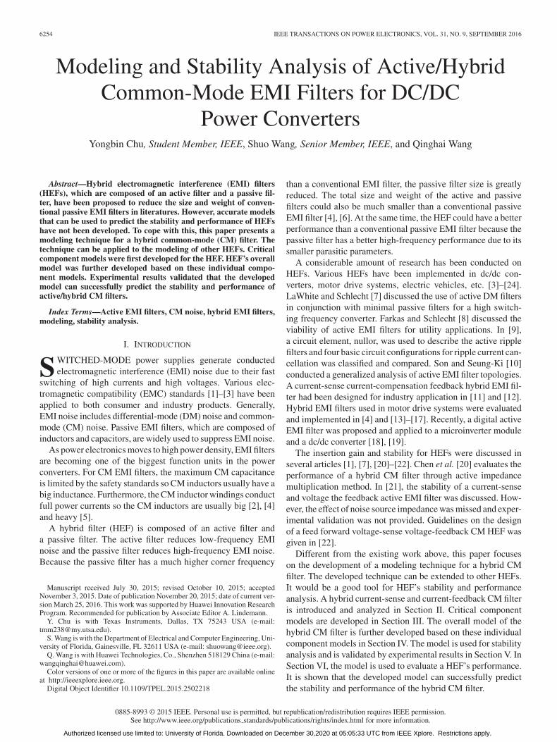
Fig. 15. CM noise measured with a 500-mV 100-kHz square wave from asignal generator noise source.
the phase margin was increased to 45° due to the presenceof RY 1 .
To further validate the stability analysis, a signal generatorwith 50 Ω source impedance was used as a noise source. A500-mV 150-kHz square wave was fed to the hybrid CM filter.The measurement results are shown in Fig. 15. Based on Fig. 13,Zc1 branch is in parallel with the noise source impedance in theloop gain calculation. In this case, the noise source impedanceis 50 Ω, which is much larger than that of Zc1 branch, soZs//Zc1 ≈ Zc1 . As a result, the loop gain of the two scenarioswith the signal generator are the same as Fig. 14. Fig. 15 agreeswith the prediction in Fig. 14. Instability occurred at 3.3 MHzif RY 1 is not connected.
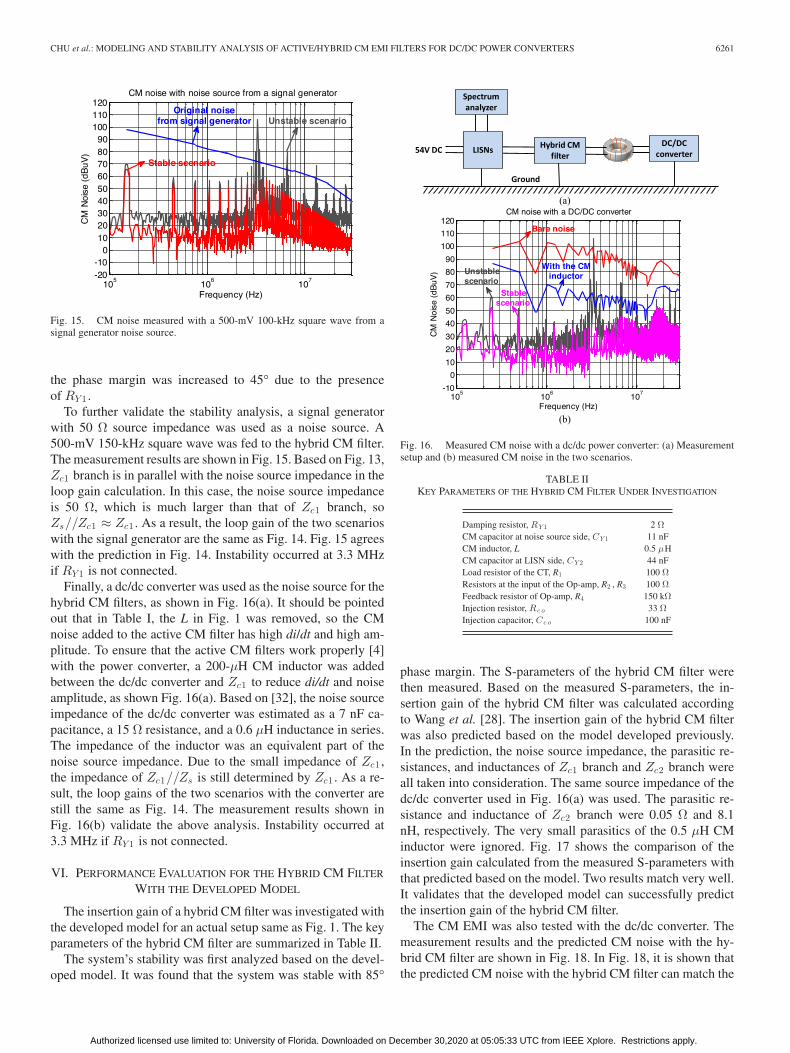
Finally, a dc/dc converter was used as the noise source for thehybrid CM filters, as shown in Fig. 16(a). It should be pointedout that in Table I, the L in Fig. 1 was removed, so the CMnoise added to the active CM filter has high di/dt and high am-plitude. To ensure that the active CM filters work properly [4]with the power converter, a 200-μH CM inductor was addedbetween the dc/dc converter and Zc1 to reduce di/dt and noiseamplitude, as shown Fig. 16(a). Based on [32], the noise sourceimpedance of the dc/dc converter was estimated as a 7 nF ca-pacitance, a 15 Ω resistance, and a 0.6 μH inductance in series.The impedance of the inductor was an equivalent part of thenoise source impedance. Due to the small impedance of Zc1 ,the impedance of Zc1//Zs is still determined by Zc1 . As a re-sult, the loop gains of the two scenarios with the converter arestill the same as Fig. 14. The measurement results shown inFig. 16(b) validate the above analysis. Instability occurred at3.3 MHz if RY 1 is not connected.
VI. PERFORMANCE EVALUATION FOR THE HYBRID CM FILTER
WITH THE DEVELOPED MODEL
The insertion gain of a hybrid CM filter was investigated withthe developed model for an actual setup same as Fig. 1. The keyparameters of the hybrid CM filter are summarized in Table II.
The system’s stability was first analyzed based on the devel-oped model. It was found that the system was stable with 85°
Fig. 16. Measured CM noise with a dc/dc power converter: (a) Measurementsetup and (b) measured CM noise in the two scenarios.
TABLE IIKEY PARAMETERS OF THE HYBRID CM FILTER UNDER INVESTIGATION
Damping resistor, RY 1 2 ΩCM capacitor at noise source side, CY 1 11 nFCM inductor, L 0.5 μHCM capacitor at LISN side, CY 2 44 nFLoad resistor of the CT, R1 100 ΩResistors at the input of the Op-amp, R2 , R3 100 ΩFeedback resistor of Op-amp, R4 150 kΩInjection resistor, Rc o 33 ΩInjection capacitor, Cc o 100 nF
phase margin. The S-parameters of the hybrid CM filter werethen measured. Based on the measured S-parameters, the in-sertion gain of the hybrid CM filter was calculated accordingto Wang et al. [28]. The insertion gain of the hybrid CM filterwas also predicted based on the model developed previously.In the prediction, the noise source impedance, the parasitic re-sistances, and inductances of Zc1 branch and Zc2 branch wereall taken into consideration. The same source impedance of thedc/dc converter used in Fig. 16(a) was used. The parasitic re-sistance and inductance of Zc2 branch were 0.05 Ω and 8.1nH, respectively. The very small parasitics of the 0.5 μH CMinductor were ignored. Fig. 17 shows the comparison of theinsertion gain calculated from the measured S-parameters withthat predicted based on the model. Two results match very well.It validates that the developed model can successfully predictthe insertion gain of the hybrid CM filter.
The CM EMI was also tested with the dc/dc converter. Themeasurement results and the predicted CM noise with the hy-brid CM filter are shown in Fig. 18. In Fig. 18, it is shown thatthe predicted CM noise with the hybrid CM filter can match the
Authorized licensed use limited to: University of Florida. Downloaded on December 30,2020 at 05:05:33 UTC from IEEE Xplore. Restrictions apply.

6262 IEEE TRANSACTIONS ON POWER ELECTRONICS, VOL. 31, NO. 9, SEPTEMBER 2016
Fig. 17. Comparison of the predicted and measured insertion gains of thehybrid CM filter.
Fig. 18. Measured and predicted CM noise.
measurement results up to 2 MHz. The high-frequency mis-match of the two results was due to other factors such as thebackground noise, grounding and near-field coupling [26], [33]–[35], etc. However, the high-frequency noise was mainly atten-uated with the passive part of the hybrid CM filter. So, thedeveloped model is very helpful in the evalution and design ofthe active part.
VII. CONCLUSION
In this paper, the model of a hybrid CM filter is developed. Themodels for CT and the operational amplifier are first developed.The model of the hybrid CM filter including the noise sourceand the load is further developed. With the developed model,the stability of the system and the performance of the hybridCM filter were effectively evaluated. The developed modelswere verified through experiments. The experimental resultsshow that the developed model can successfully predict thestability and low-frequency performance of the hybrid CM filter.This would greatly benefit the design and application of thehybrid CM filters in power electronics systems. The proceduredeveloped in this paper can be used to model other types ofHEFs.
REFERENCES
[1] K. Mainali and R. Oruganti, “Conducted EMI Mitigation techniques forswitch-mode power converters: A survey,” IEEE Trans. Power Electron.,vol. 25, no. 9, pp. 2344–2356, Sep. 2010.
[2] R. P. Clayton, Introduction to Electromagnetic Compatibility, 2nd ed.Hoboken, NJ, USA: Wiley, 2006.
[3] M. Ali, E. Laboure, and F Costa, “Integrated active filter for differential-mode noise suppression,” IEEE Trans. Power Electron., vol. 29, no. 3,pp. 1053–1057, Mar. 2014.
[4] S. Wang, Y. Y. Maillet, F. Wang, D. Boroyevich, and R. Burgos, “In-vestigation of hybrid EMI filters for common-mode EMI suppressionin a motor drive system,” IEEE Trans. Power Electron., vol. 25, no. 4,pp. 1034–1045, Apr. 2010.
[5] W. Chen, W. Zhang, X. Yang, Z. Sheng, and Z. Wang, “An experimentalstudy of common- and differential-mode Active EMI filter compensa-tion characteristics,” IEEE Trans. Electromagn. Compat., vol. 51, no. 3,pp. 683–691, Aug. 2009.
[6] W. Chen, X. Yang, and Z. Wang, “An active EMI filtering techniquefor improving passive filter low-frequency performance,” IEEE Trans.Electromagn. Compat., vol. 48, no. 1, pp. 172–177, Feb. 2006.
[7] L. LaWhite and M. F. Schlecht, “Design of active ripple filters for powercircuits operating in the 1–10 MHz range,” IEEE Trans. Power Electron.,vol. 3, no. 3, pp. 310–317, Jul. 1988.
[8] T. Farkas and M. F. Schlecht, “Viability of active EMI filters for utilityapplications,” IEEE Trans. Power Electron., vol. 9, no. 3, pp. 328–337,May 1994.
[9] N. K. Poon, J. C. P. Liu, C. K. Tse, and M. H. Pong, “Techniques for in-put ripple current cancellation: classification and implementati-on,” IEEETrans. Power Electron., vol. 15, no. 6, pp. 1144–1152, Nov. 2000.
[10] Y.-C. Son and S. Seung-Ki, “Generalization of active filters for EMIreduction and harmonics compensation,” IEEE Trans. Ind. Appl., vol. 42,no. 2, pp. 545–551, Mar./Apr. 2006.
[11] J. Dumas, B. Lanoue, and B. Tahhan, “Active analog power filters providesolutions for EMC and EMI,” in Proc. IEEE Appl. Power Electron. Conf.,2004, pp. 675–680.
[12] M. Briere, J. Dumas, and B. Tahhan, “EMI filter circuit,” U.S. Patent 6898 092 B2, May 24, 2005.
[13] M. C. Di Piazza, A. Ragusa, and G. Vitale, “An optimized feedbackcommon mode active filter for vehicular induction motor drives,” IEEETrans. Power Electron., vol. 26, no. 11, pp. 3153–3162, Nov. 2011.
[14] W. Chen, X. Yang, J. Xue, and F. Wang, “A novel filter topology with activemotor CM impedance regulator in PWM ASD system,” IEEE Trans. Ind.Electron., vol. 61, no. 12, pp. 6938–6946, Dec. 2014.
[15] P. Pairodamonchai, S. Suwankawin, and S. Sangwongwanich, “Design andimplementation of a hybrid output EMI filter for high-frequency common-mode voltage compensation in PWM inverters,” IEEE Trans. Ind. Appl.,vol. 45, no. 5, pp. 1647–1659, Sep./Oct. 2009.
[16] M. C. Di Piazza, M. Luna, and G. Vitale, “EMI reduction in DC-fed electricdrives by active common-mode compensator,” IEEE Trans. Electromagn.Compat., vol. 56, no. 5, pp. 1067–1076, Oct. 2014.
[17] C. Zhu and T. H. Hubing, “An active cancellation circuit for reducingelectrical noise from three-phase AC motor drivers,” IEEE Trans. Electro-magn. Compat., vol. 56, no. 1, pp. 60–66, Feb. 2014.
[18] D. Hamza, Q. Mei, and P. K. Jain, “Application and stability analysisof a novel digital active EMI filter used in a grid-tied PV microinvertermodule,” IEEE Trans. Power Electron., vol. 28, no. 6, pp. 2867–2874,Jun. 2013.
[19] D. Hamza, M. Pahlevaninezhad, and P. K. Jain, “Implementation of a noveldigital active EMI technique in a DSP-based DC–DC digital controllerused in electric vehicle (EV),” IEEE Trans. Power Electron., vol. 28,no. 7, pp. 3126–3137, Jul. 2013.
[20] W. Chen, X. Yang, and Z. Wang, “A novel hybrid common-mode EMIfilter with active impedance multiplication,” IEEE Trans. Ind. Electron.,vol. 58, no. 5, pp. 1826–1834, May 2011.
[21] K. Mainali and R. Oruganti, “Design of a current-sense voltage-feedbackcommon mode EMI filter for an off-line power converter,” in Proc. IEEEPower Electron. Spec. Conf., 2008, pp. 1632–1638.
[22] D. Shin, S. Kim, G. Jeong, J. Park, J, Park, K. J. Han, and J. Kim, “Analysisand design guide of active EMI filter in a compact package for reductionof common-mode conducted emissions,” IEEE Trans. Electromagn. Com-pat., vol. 57, no. 4, pp. 660–671, Aug. 2015.
[23] X. Chang, W. Chen, Y. Yang, K. Wang, and X. Yang, “Research andrealization of a novel active common-mode EMI filter,” in Proc. IEEEAppl. Power Electron. Conf., 2015, pp. 1941–1945.
Authorized licensed use limited to: University of Florida. Downloaded on December 30,2020 at 05:05:33 UTC from IEEE Xplore. Restrictions apply.
CHU et al.: MODELING AND STABILITY ANALYSIS OF ACTIVE/HYBRID CM EMI FILTERS FOR DC/DC POWER CONVERTERS 6263
[24] D. Hamza, M. Sawan, and P. K. Jain, “Suppression of common-modeinput electromagnetic interference noise in DC-DC converters usingthe active filtering method,” IET Trans. Power Electron., vol. 4, no. 7,pp. 776–784, Aug. 2011.
[25] N. Kondrath and M. K. Kazimierczuk, “Bandwidth of current trans-formers,” IEEE Trans. Instrum. Meas., vol. 58, no. 6, pp. 2008–2016,Jun. 2009.
[26] Y. Chu, S. Wang, N. Zhang, and D. Fu, “A common mode inductorwith external magnetic field immunity, low magnetic field emission andhigh differential mode inductance,” IEEE Trans. Power Electron., vol. 30,no. 12, pp. 6684–6694, Dec. 2015.
[27] Y. Chu and S. Wang, “A generalized common-mode current cancela-tion approach for power converters,” IEEE Trans. Ind. Electron., vol. 62,no. 7, pp. 4130–4140, Jul. 2015.
[28] S. Wang, F. C. Lee, and W. G. Odendaal, “Characterization and parasiticextraction of EMI filters using scattering parameters,” IEEE Trans. PowerElectron., vol. 20, no. 2, pp. 502–510, Mar. 2005.
[29] S. Wang, F. C. Lee, and W. G. Odendaal, “Using scattering parametersto characterize EMI filters,” in Proc. IEEE Power Electron. Spec. Conf.,2004, pp. 297–303.
[30] E. Sanchez-Sinencio and M. L. Majewski, “A nonlinear macromodel ofoperational amplifiers in the frequency domain,” IEEE Trans. CircuitsSyst., vol. CAS-26, no. 6, pp. 395–402, Jun. 1979.
[31] P. R. Gray, P. J. Hurst, S. H. Lewis, and R. G. Meyer, Analysis and Designof Analog Intergrated Circuits. New York, NY, USA: Wiley, 2009
[32] D. Zhang, D. Y. Chen, M. J. Nave, and D. Sable, “Measurement of noisesource impedance of off-line converters,” IEEE Trans. Power Electron.,vol. 15, no. 5, pp. 820–825, Sep. 2000.
[33] Y. Chu, S. Wang, J. Xu, and D. Fu, “EMI reduction with near field cou-pling suppression techniques for planar transformers and CM chokes inswitching-mode power converters,” in Proc. IEEE Energy Convers. Congr.Expo., 2013, pp. 3679–3686.
[34] S. Wang, Y. Y Maillet, F. Wang, R. Lai, F. Luo, and D. Boroyevich,“Parasitic effects of grounding paths on common-mode EMI filter’s per-formance in power electronics systems,” IEEE Trans. Ind. Electron.,vol. 57, no. 9, pp. 3050–3059, Sep. 2010.
[35] S. Wang, J. D. Van Wyk, and F. C. Lee, “Effects of interactions betweenfilter parasitics and power interconnects on EMI filter performance,” IEEETrans. Ind. Electron., vol. 54, no. 6, pp. 3344–3352, Dec. 2007.
Yongbin Chu (S’12) received the B.S.E.E. degreefrom the Hefei University of Technology, Hefei,China, in 2011, and the Ph.D. degree from the Uni-versity of Texas at San Antonio, San Antonio, TX,USA, in 2015.
His interest includes circuit topology for powerelectronics, EMI/EMC in power electronics systems,high-efficiency and high power density power conver-sion, and power systems analysis. He has publishedmore than ten IEEE journal and conference papers.
Shuo Wang (S’03–M’06–SM’07) received the Ph.D.degree from Virginia Tech, Blacksburg, VA, USA, in2005.
He has been an Associate Professor at the Depart-ment of Electrical and Computer Engineering, Uni-versity of Florida, Gainesville, FL, USA, since 2015.From 2010 to 2014, he was with the University ofTexas at San Antonio, San Antonio, TX, USA, firstas an Assistant Professor and later as an AssociateProfessor. From 2009 to 2010, he was a Senior De-sign Engineer with GE Aviation Systems, Vandalia,
OH, USA. From 2005 to 2009, he was a Research Assistant Professor withVirginia Tech. He has published more than 110 IEEE journal and conferencepapers and holds seven U.S. patents.
Dr. Wang received the Best Transaction Paper Award from the IEEE PowerElectronics Society in 2006 and two William M. Portnoy Awards for the pa-pers published in the IEEE Industry Applications Society in 2004 and 2012,respectively. In 2012, he received the prestigious National Science FoundationCAREER Award. He is an Associate Editor for the IEEE TRANSACTIONS ON
INDUSTRY APPLICATIONS and a Technical Program Cochair for the IEEE 2014International Electric Vehicle Conference.
Qinghai Wang received the B.Eng. degree in elec-trical engineering from Xi’an Jiaotong University,Xi’an, China, in 2001.
After graduation, he was with Huawei Technolo-gies, Co., Ltd., Shenzhen, China, where he was in-volved in EMC and Surge protection design and re-search for ICT& Power module. He is currently aChief Design Engineer and the Leader of EMC andLightning Technology Manage Group. He had madeoutstanding contributions to protection circuit design,the miniaturization of protection and filter circuits, LF
filter design and grounding design, etc. His current research interest includesEMI modeling and system simulation, EMI suppression, and passive and activefilter design for power electronic product. He is a Member of several standardorganizations and has been responsible for the constituting of several standards,and holds 12 patents.
Authorized licensed use limited to: University of Florida. Downloaded on December 30,2020 at 05:05:33 UTC from IEEE Xplore. Restrictions apply.