an integrated active hybrid filter for adsl
TRANSCRIPT
An Integrated Active Hybrid Filter for ADSL
Jim Hellums, Ph.D.TI Fellow
Seminar for IEEEMay 29, 2008

I wish to acknowledge collaborations with:
Dr. Richard HesterTI Senior Fellow
Outline
•Background•System•Circuits•Process•Measurements•Summary

ADSL System
Transmitter
Receiver
Transmitter
Receiver
DOWN <= 8 Mbps
UP <= 800 kbps
POTSSplitter
POTSSplitter
up to 19 kft
Central Office Remote Terminal
PSTN
Subscriber Loop
POTS
1.1 MHzFrequency
Frequency Division Multiplexed Operation
26 kHz
DownUp
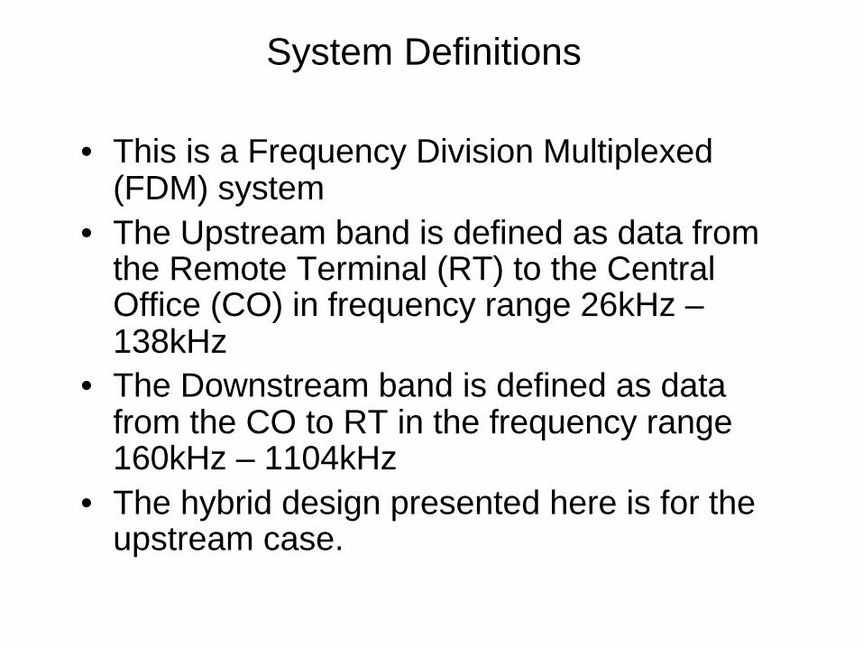
System Definitions
• This is a Frequency Division Multiplexed (FDM) system
• The Upstream band is defined as data from the Remote Terminal (RT) to the Central Office (CO) in frequency range 26kHz –138kHz
• The Downstream band is defined as data from the CO to RT in the frequency range 160kHz –1104kHz
• The hybrid design presented here is for the upstream case.
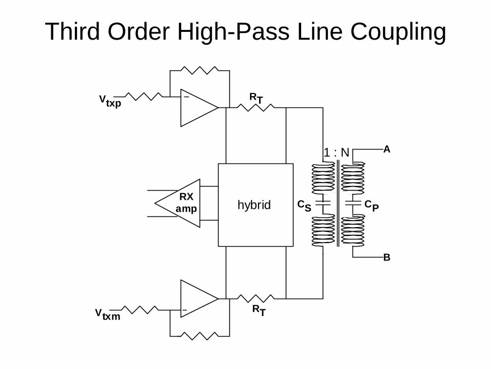
Third Order High-Pass Line Coupling
Vtxp
Vtxm
B
1 : N
RXamp
RT
RT
CS CP
A
hybrid
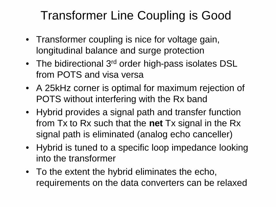
Transformer Line Coupling is Good
• Transformer coupling is nice for voltage gain, longitudinal balance and surge protection
• The bidirectional 3rd order high-pass isolates DSL from POTS and visa versa
• A 25kHz corner is optimal for maximum rejection of POTS without interfering with the Rx band
• Hybrid provides a signal path and transfer function from Tx to Rx such that the net Tx signal in the Rx signal path is eliminated (analog echo canceller)
• Hybrid is tuned to a specific loop impedance looking into the transformer
• To the extent the hybrid eliminates the echo, requirements on the data converters can be relaxed
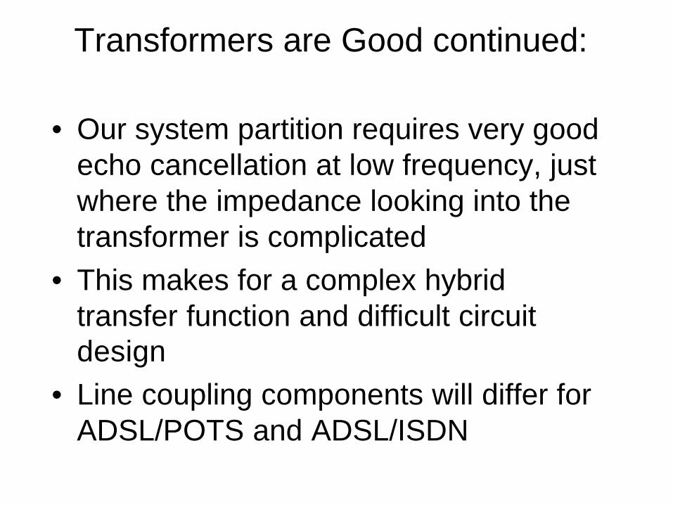
Transformers are Good continued:
•Our system partition requires very good echo cancellation at low frequency, just where the impedance looking into the transformer is complicated
•This makes for a complex hybrid transfer function and difficult circuit design
•Line coupling components will differ for ADSL/POTS and ADSL/ISDN
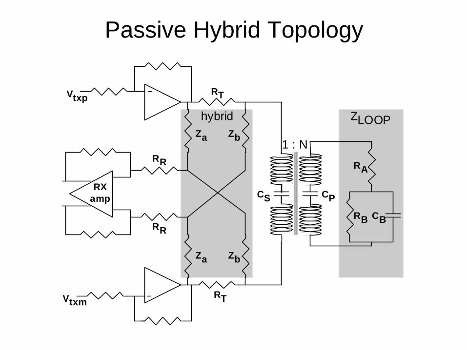
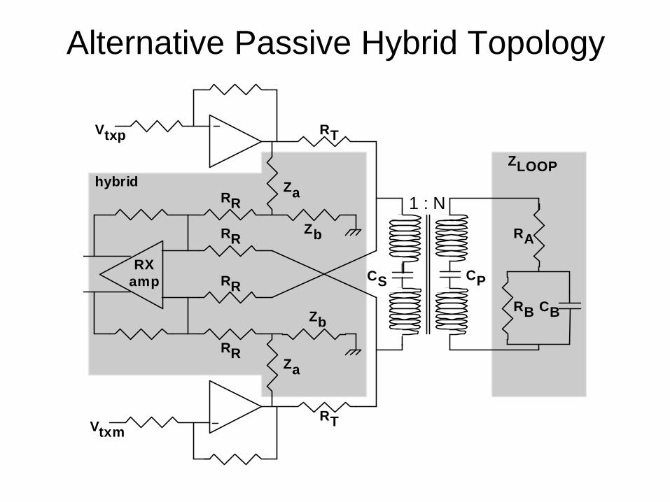
Passive Hybrid Topology
Vtxp
Vtxm
RB
1 : NZa
Za Zb
Zb
hybrid
RXamp
RR
RT
RT
RR
ZLOOP
CS CP
CB
RA
A Bridge as Hybrid
•A Bridge circuit cancels the echo by construction
•Ideally the Rx amp only amplifies the receive signal
•The Bridge is tuned to the line coupling and loop impedance
•The Z-Loop model is not exact, but good enough to calculate Za & Zb
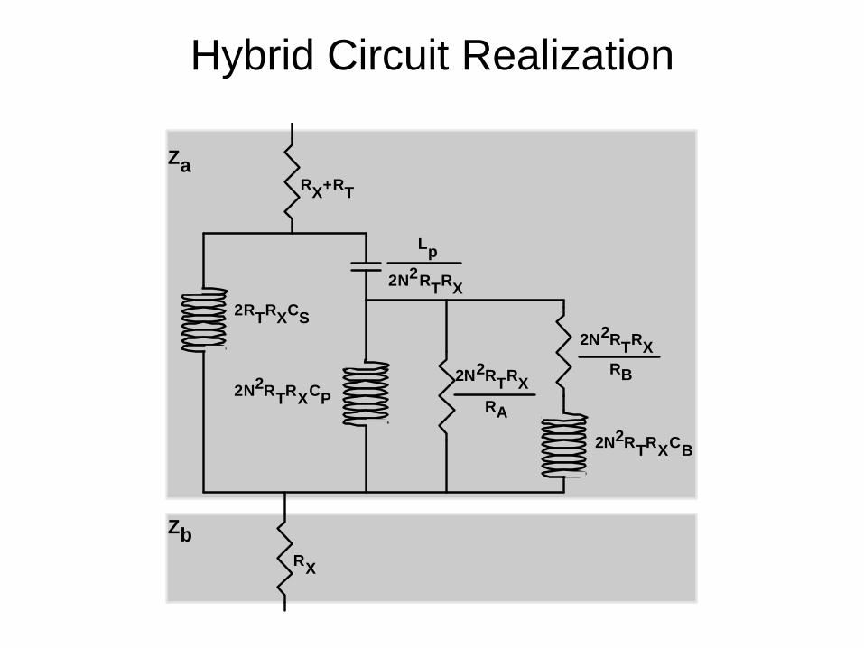
Hybrid Circuit Realization
Lp
2N2RTRX
Zb
Za
RX
RX+RT
RB
2N2RTRX
2N2RTRXCB
RA
2N2RTRX
2RTRXCS
2N2RTRXCP
Circuit Realization Comments
•The exact equation solution for the Bridge component values exits
•Complicated: requires 4 resistors, 3 inductors and 1 capacitors
•Large cost and board area•Inductors must be non-saturating and
Capacitors have the best dielectric to be distortion free
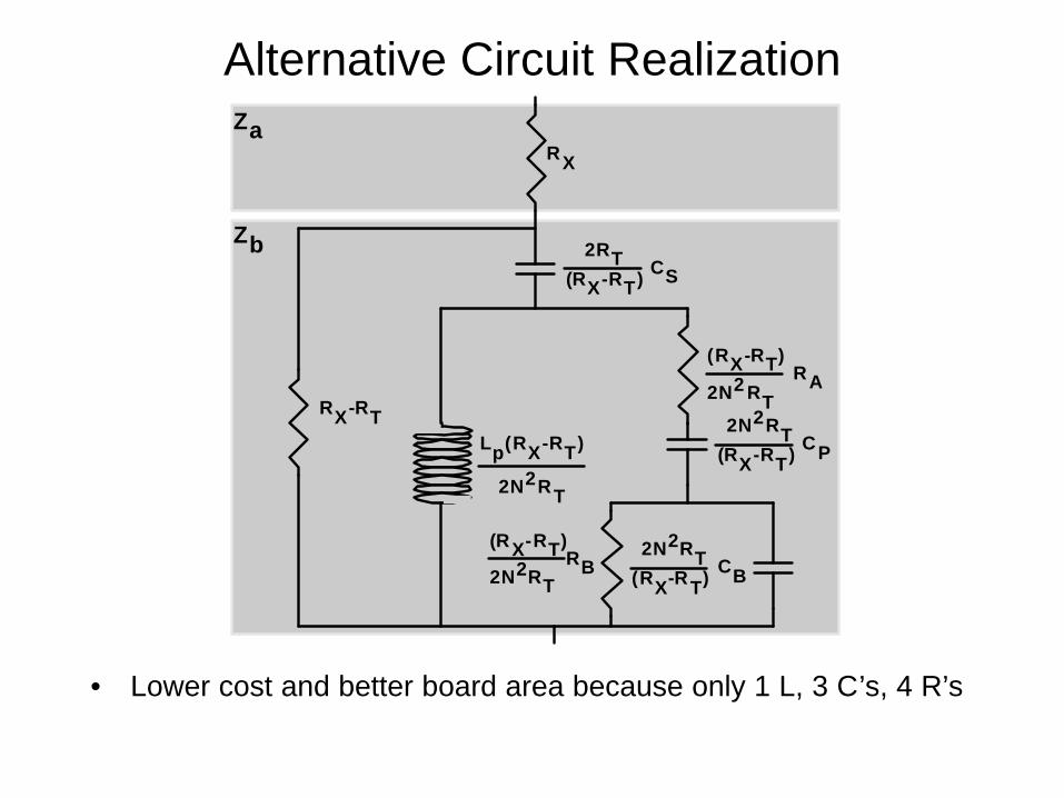
Alternative Circuit RealizationZa
Zb
RX-RT
RX
2N2RT
Lp(RX-RT)
2N2RT
(RX-RT)RB
2N2RT(RX-RT)
CP
2N2 RT
(RX-RT)RA
2RT(RX-RT)
CS
2N2RT(RX-RT)
CB
• Lower cost and better board area because only 1 L, 3 C’s, 4 R’s
Alternative Passive Hybrid Topology
Vtxp
Vtxm
RB
1 : NZa
Za
Zb
Zb
hybrid
RXamp
RR
RT
RT
RR
ZLOOP
CS CP
CB
RARR
RR
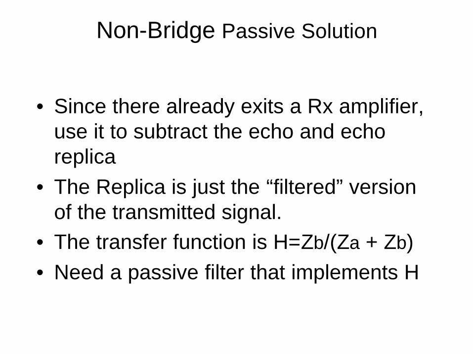
Non-Bridge Passive Solution
•Since there already exits a Rx amplifier, use it to subtract the echo and echo replica
•The Replica is just the “filtered”version of the transmitted signal.
•The transfer function is H=Zb/(Za + Zb)•Need a passive filter that implements H
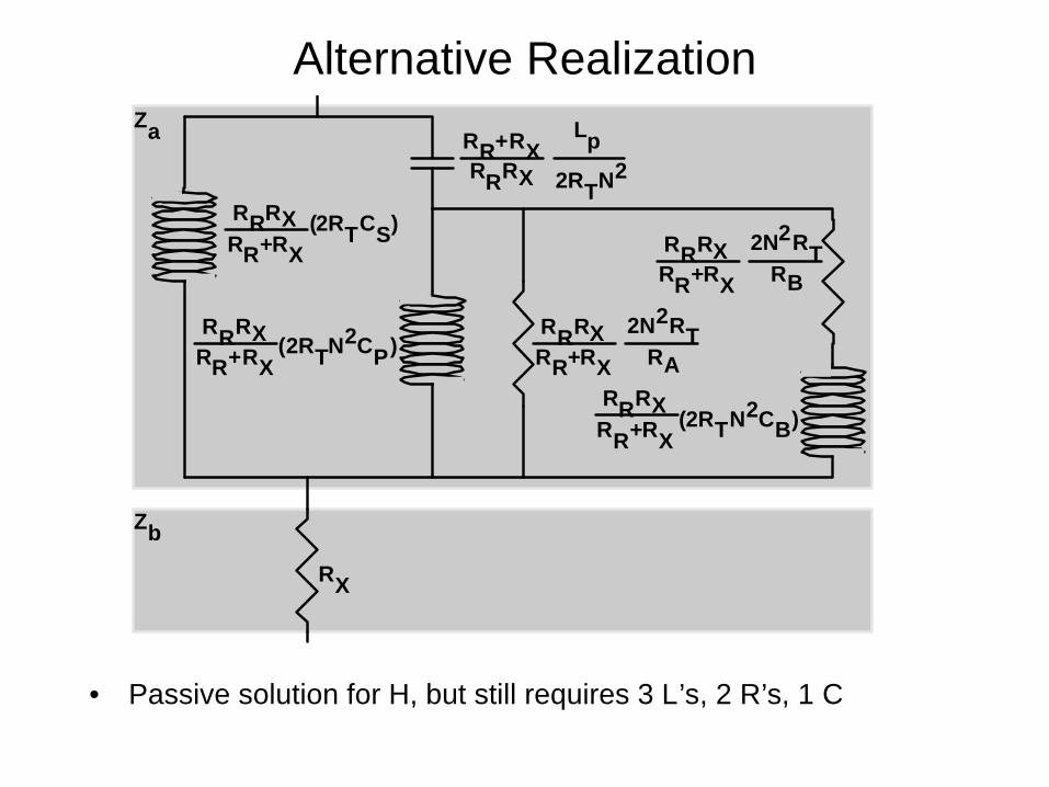
Alternative RealizationLp
2RTN2
Zb
Za
RX
RA
2N2RT
(2RTCS)
RR+RXRRRX
RR+RX
RRRX
RR+RX
RRRX (2RTN2CP) RR+RX
RRRX
RB
2N2RTRR+RX
RRRX
RR+RX
RRRX(2RTN2CB)
• Passive solution for H, but still requires 3 L’s, 2 R’s, 1 C
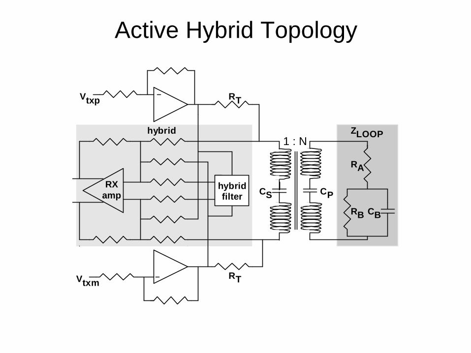
Active Hybrid Topology
Vtxp
Vtxm
RB
1 : Nhybrid
RXamp
RT
RT
ZLOOP
CS CP
CB
RA
hybridfilter
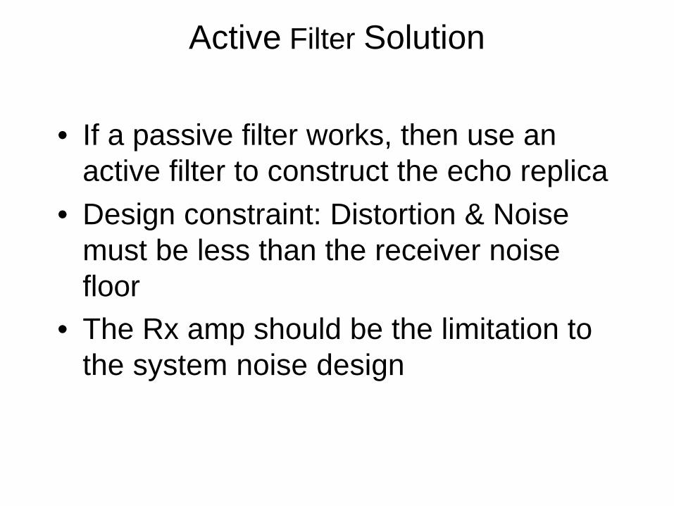
Active Filter Solution
•If a passive filter works, then use an active filter to construct the echo replica
•Design constraint: Distortion & Noise must be less than the receiver noise floor
•The Rx amp should be the limitation to the system noise design
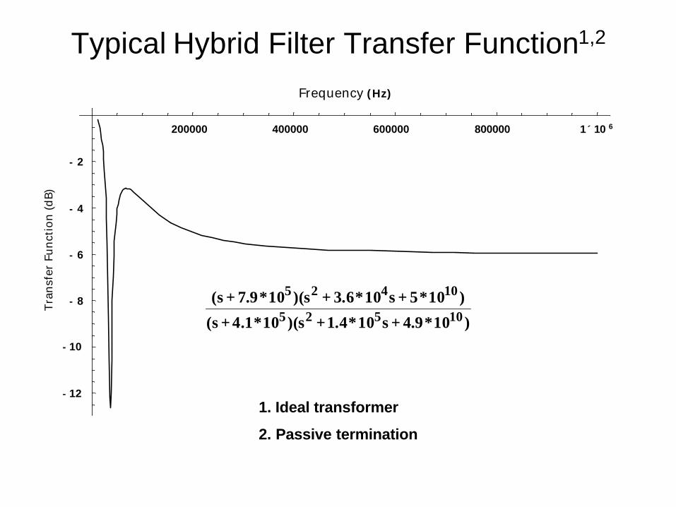
Typical Hybrid Filter Transfer Function1,2
200000 400000 600000 800000 1´ 10 6
- 12
- 10
- 8
- 6
- 4
- 2
Frequency (Hz)
Tran
sfer
Fun
ctio
n (d
B)
)10*9.4s10*4.1s)(10*1.4s(
)10*5s10*6.3s)(10*9.7s(10525
10425
+++
+++
1. Ideal transformer
2. Passive termination
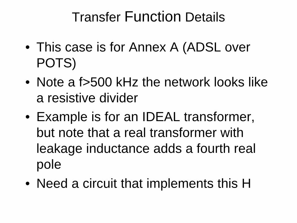
Transfer Function Details
•This case is for Annex A (ADSL over POTS)
•Note a f>500 kHz the network looks like a resistive divider
•Example is for an IDEAL transformer, but note that a real transformer with leakage inductance adds a fourth real pole
•Need a circuit that implements this H
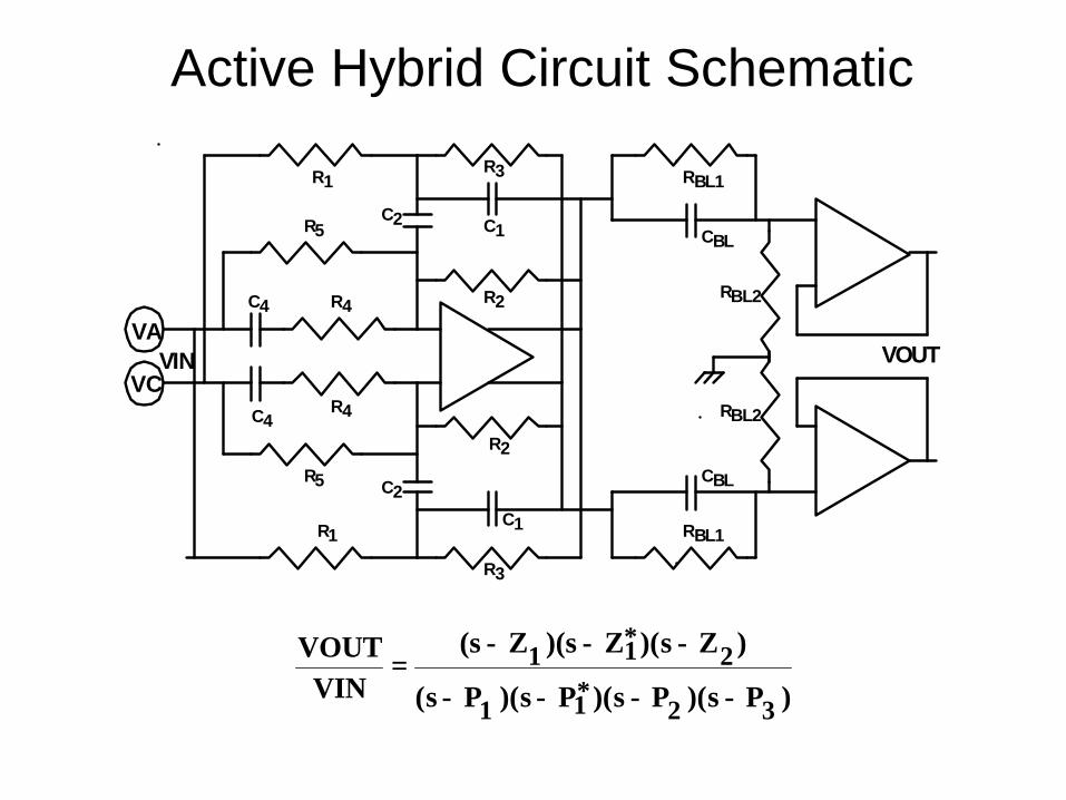
)Ps)(Ps)(Ps)(Ps(
)Zs)(Zs)(Zs(
VINVOUT
32*11
2*11
−−−−
−−−=
VIN
C1
R3R1
C2R5
C4 R2
C2
R3
C1
R2
R5
C4
R1
R4
R4
VOUT
CBL
RBL1
CBL
RBL2
RBL1
RBL2
VA
VC
Active Hybrid Circuit Schematic
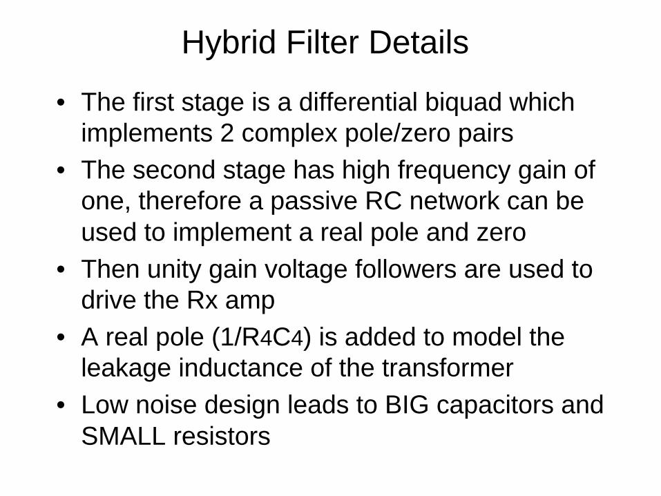
Hybrid Filter Details
• The first stage is a differential biquad which implements 2 complex pole/zero pairs
• The second stage has high frequency gain of one, therefore a passive RC network can be used to implement a real pole and zero
• Then unity gain voltage followers are used to drive the Rx amp
• A real pole (1/R4C4) is added to model the leakage inductance of the transformer
• Low noise design leads to BIG capacitors and SMALL resistors
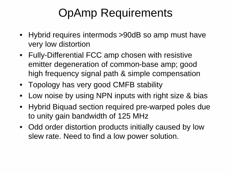
OpAmp Requirements
• Hybrid requires intermods >90dB so amp must have very low distortion
• Fully-Differential FCC amp chosen with resistive emitter degeneration of common-base amp; good high frequency signal path & simple compensation
• Topology has very good CMFB stability• Low noise by using NPN inputs with right size & bias• Hybrid Biquad section required pre-warped poles due
to unity gain bandwidth of 125 MHz• Odd order distortion products initially caused by low
slew rate. Need to find a low power solution.
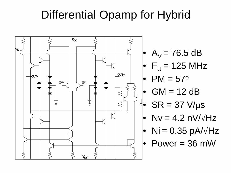
Differential Opamp for Hybrid
• AV = 76.5 dB• FU = 125 MHz• PM = 57o
• GM = 12 dB• SR = 37 V/µs• Nv = 4.2 nV/√Hz• Ni = 0.35 pA/√Hz• Power = 36 mW
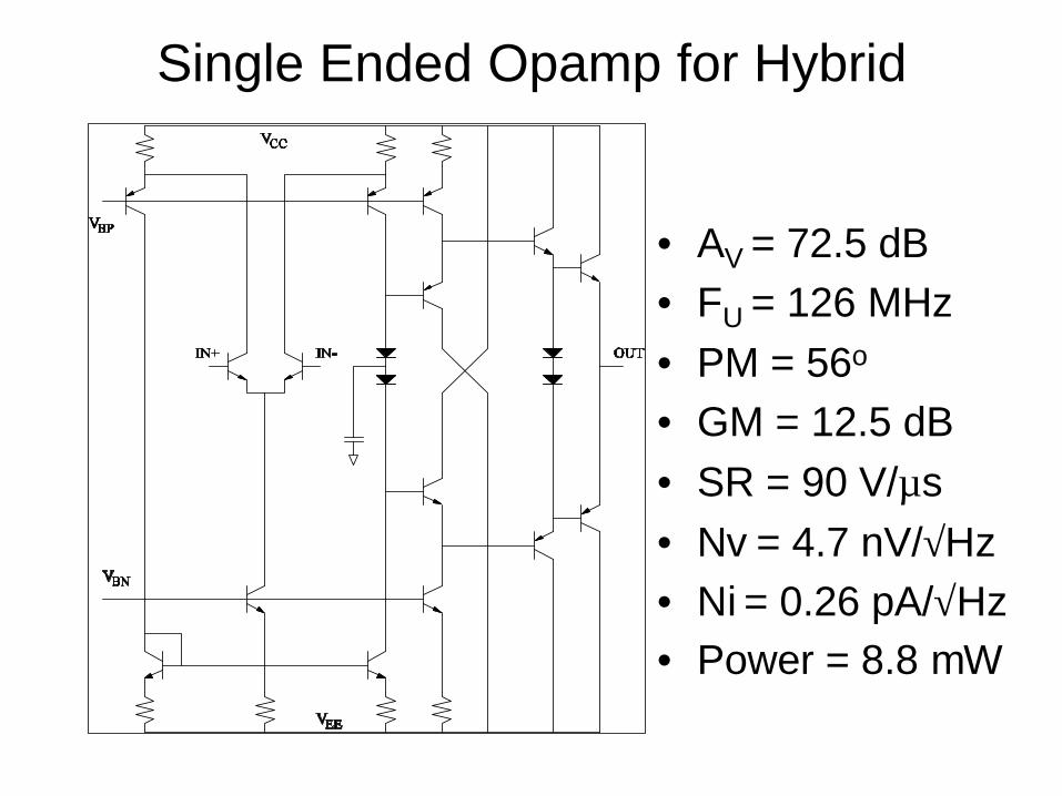
Single Ended Opamp for Hybrid
• AV = 72.5 dB• FU = 126 MHz• PM = 56o
• GM = 12.5 dB• SR = 90 V/µs• Nv = 4.7 nV/√Hz• Ni = 0.26 pA/√Hz• Power = 8.8 mW
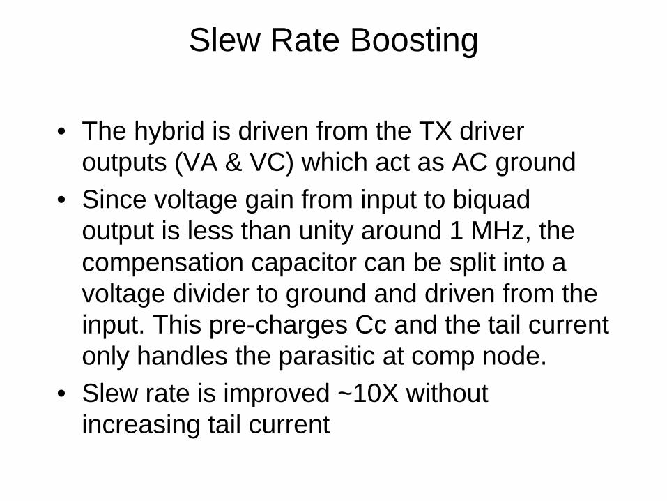
Slew Rate Boosting
• The hybrid is driven from the TX driver outputs (VA & VC) which act as AC ground
• Since voltage gain from input to biquadoutput is less than unity around 1 MHz, the compensation capacitor can be split into a voltage divider to ground and driven from the input. This pre-charges Cc and the tail current only handles the parasitic at comp node.
• Slew rate is improved ~10X without increasing tail current
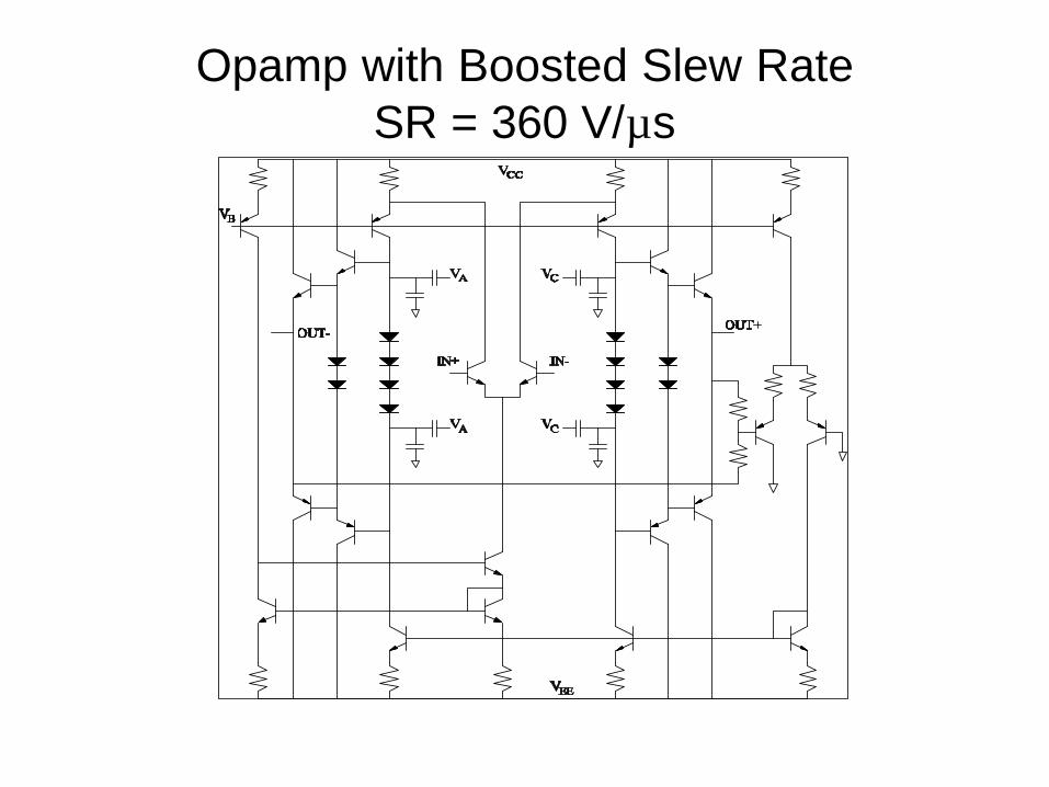
Opamp with Boosted Slew RateSR = 360 V/µs
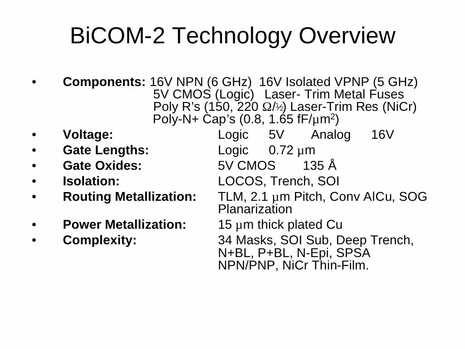
BiCOM-2 Technology Overview
• Components: 16V NPN (6 GHz) 16V Isolated VPNP (5 GHz)5V CMOS (Logic) Laser- Trim Metal Fuses Poly R’s (150, 220 Ω / ) Laser-Trim Res (NiCr)Poly-N+ Cap’s (0.8, 1.65 fF/µm2)
• Voltage: Logic ⇒ 5V Analog ⇒ 16V• Gate Lengths: Logic ⇒ 0.72 µm • Gate Oxides: 5V CMOS ⇒ 135 Å• Isolation: LOCOS, Trench, SOI• Routing Metallization: TLM, 2.1 µm Pitch, Conv AlCu, SOG
Planarization• Power Metallization: 15 µm thick plated Cu • Complexity: 34 Masks, SOI Sub, Deep Trench,
N+BL, P+BL, N-Epi, SPSA NPN/PNP, NiCr Thin-Film.
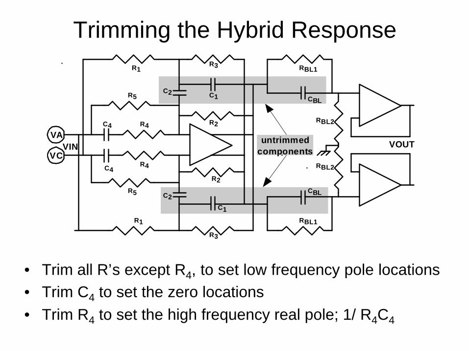
VIN
C1
R3R1
C2R5
C4 R2
C2
R3
C1
R2
R5
C4
R1
R4
R4
VOUT
CBL
RBL1
CBL
RBL2
RBL1
RBL2
untrimmedcomponents
VA
VC
Trimming the Hybrid Response
• Trim all R’s except R4, to set low frequency pole locations• Trim C4 to set the zero locations• Trim R4 to set the high frequency real pole; 1/ R4C4
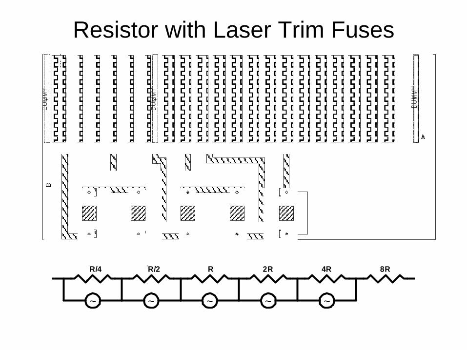
Resistor with Laser Trim Fuses
8R4R2RRR/2R/4
~ ~~ ~ ~
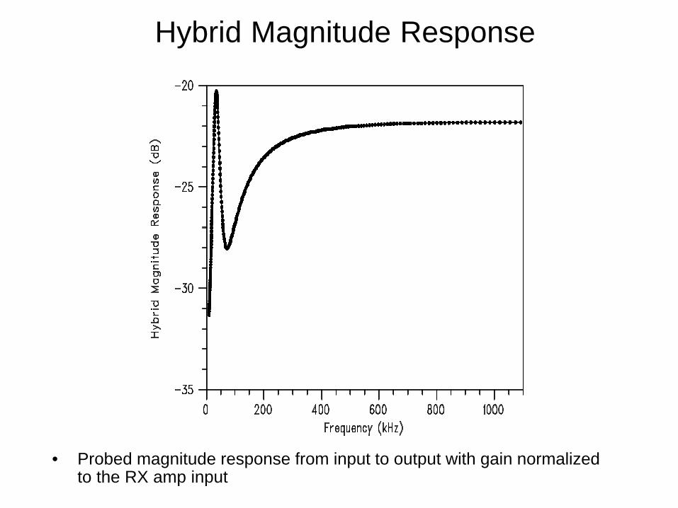
Hybrid Magnitude Response
• Probed magnitude response from input to output with gain normalized to the RX amp input
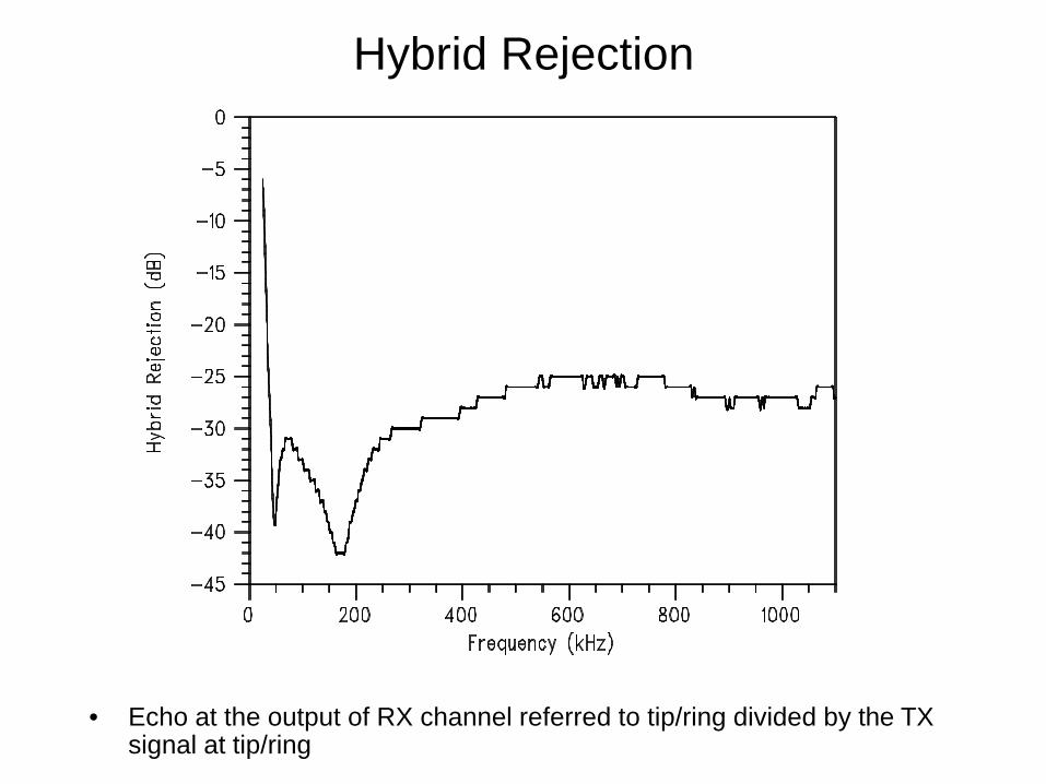
Hybrid Rejection
• Echo at the output of RX channel referred to tip/ring divided by the TX signal at tip/ring
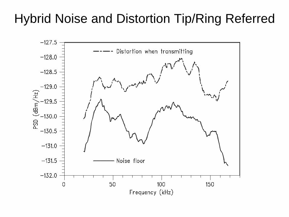
Hybrid Noise and Distortion Tip/Ring Referred
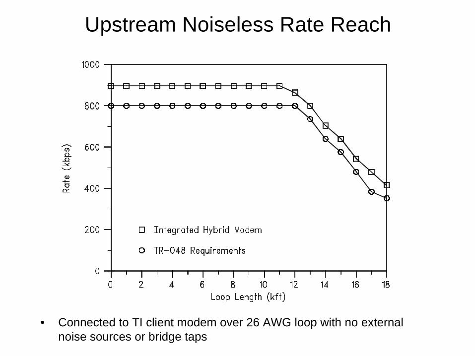
Upstream Noiseless Rate Reach
• Connected to TI client modem over 26 AWG loop with no external noise sources or bridge taps
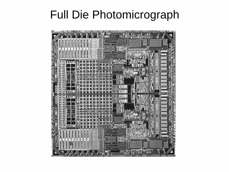
Full Die Photomicrograph
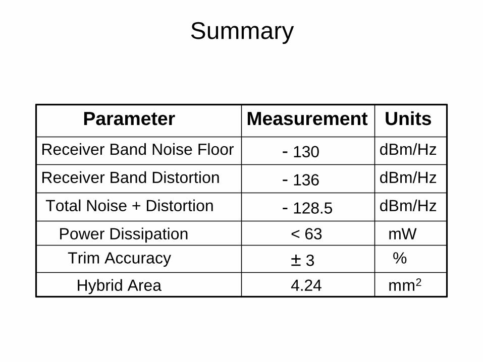
Summary
mm24.24Hybrid Area
UnitsMeasurementParameter
%±3Trim AccuracymW< 63Power Dissipation
dBm/Hz- 128.5Total Noise + Distortion
dBm/Hz- 136Receiver Band Distortion
dBm/Hz- 130Receiver Band Noise Floor