for thin film e-beam, deep uv or uv lithography

1
www.microresist.com For Thin Film E-Beam, Deep UV or UV Lithography Main applications Use in micro- and nanoelectronics Manufacturing of semiconductor devices Mask for etching, e.g. Si, SiO 2 , Si 3 N 4 or metals Generation of sub 100 nm pattern Generation of stamps with nanopatterns 500 nm thick, 1000 nm chess pattern 100 nm thick, 50 nm L/ S 100 nm thick, 80 nm dots 100 nm thick, 80 nm L/ S mr-EBL 6000 (All pictures - Courtesy of IPHT/ Jena and Fraunhofer - HHI/ Berlin) Resist ma-N 2400 mr-EBL 6000 mr-UVL 6000 Exposure dose @ 10 keV E-beam @ 20 keV @ 50 keV Deep UV [248 nm/ 254 nm] UV [300 365 nm] - 120 – 250 µC/cm 2 100 – 350 µC/cm 2 210 – 420 mJ/cm 2 - 2 – 5 µC/cm 2 4 – 6 µC/cm 2 20 – 40 µC/cm 2 - - - - - - 400 – 550 mJ/cm 2 Ready-to-use solutions for various film thicknesses @ 3000 rpm ma-N 2401 g 0.1 µm ma-N 2403 g 0.3 µm ma-N 2405 g 0.5 µm ma-N 2410 g 1.0 µm mr-EBL 6000.1 g 0.1 µm mr-EBL 6000.3 g 0.3 µm mr-EBL 6000.5 g 0.5 µm mr-UVL 6000.1 g 0.1 µm mr-UVL 6000.3 g 0.3 µm mr-UVL 6000.5 g 0.5 µm Developer ma-D 525 (TMAH based) ma-D 332/ ma-D 331 (NaOH based) mr-Dev 600 (solvent based) ma-N 2400 and mr-EBL 6000 for pattern transfer These two series are mainly used for electron beam lithography. mr-UVL 6000 for pattern transfer Mainly used for thin layer UV lithography. High dry and wet etch resistance Excellent thermal stability of the resist patterns Post exposure bake (PEB) ma-N 2400 e-beam & Deep UV sensitive High resolution capability Aqueous alkaline development Good thermal stability of the resist patterns High wet and dry etch resistance Lift-off Easy to remove mr-EBL 6000 high e-beam sensitivity Excellent thermal stability of the resist patterns High dry and wet etch resistance High resolution capability Post exposure bake (PEB) Photoresist Substrate (Si) Substrate (SiO ) 2 Coat, Softbake E-beam exposure (+ PEB for mr-EBL 6000) Develop Crosslinked Photoresist RIE Resist Removal ma-N 2400 3

Upload: others

Post on 29-Nov-2021

2 views

Category:

Documents


0 download

TRANSCRIPT

w

ww

.micr

ores

ist.c

om

For Thin Film E-Beam, Deep UV or UV Lithography

Main applications • Use in micro- and nanoelectronics • Manufacturing of semiconductor devices • Mask for etching, e.g. Si, SiO2, Si3N4 or metals • Generation of sub 100 nm pattern • Generation of stamps with nanopatterns

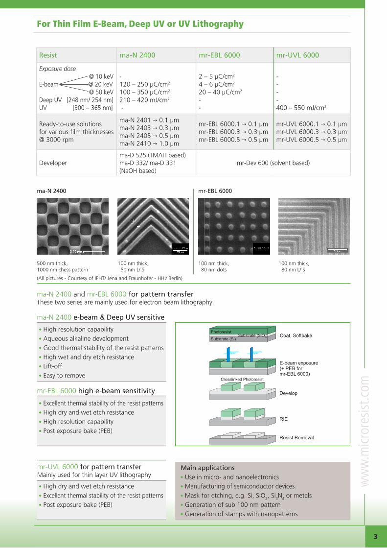
500 nm thick,1000 nm chess pattern

100 nm thick, 50 nm L/ S

100 nm thick, 80 nm dots

100 nm thick, 80 nm L/ S

mr-EBL 6000

(All pictures - Courtesy of IPHT/ Jena and Fraunhofer - HHI/ Berlin)

Resist ma-N 2400 mr-EBL 6000 mr-UVL 6000

Exposure dose @ 10 keVE-beam @ 20 keV @ 50 keVDeep UV [248 nm/ 254 nm]UV [300 – 365 nm]

-120 – 250 µC/cm2

100 – 350 µC/cm2

210 – 420 mJ/cm2

-

2 – 5 µC/cm2

4 – 6 µC/cm2

20 – 40 µC/cm2

--

-- --400 – 550 mJ/cm2

Ready-to-use solutions for various film thicknesses @ 3000 rpm

ma-N 2401 g 0.1 µmma-N 2403 g 0.3 µmma-N 2405 g 0.5 µmma-N 2410 g 1.0 µm

mr-EBL 6000.1 g 0.1 µmmr-EBL 6000.3 g 0.3 µmmr-EBL 6000.5 g 0.5 µm

mr-UVL 6000.1 g 0.1 µmmr-UVL 6000.3 g 0.3 µmmr-UVL 6000.5 g 0.5 µm

Developerma-D 525 (TMAH based) ma-D 332/ ma-D 331 (NaOH based)

mr-Dev 600 (solvent based)

ma-N 2400 and mr-EBL 6000 for pattern transfer These two series are mainly used for electron beam lithography.

mr-UVL 6000 for pattern transferMainly used for thin layer UV lithography.

• High dry and wet etch resistance • Excellent thermal stability of the resist patterns• Post exposure bake (PEB)

ma-N 2400 e-beam & Deep UV sensitive

• High resolution capability • Aqueous alkaline development• Good thermal stability of the resist patterns• High wet and dry etch resistance• Lift-off• Easy to remove

mr-EBL 6000 high e-beam sensitivity

• Excellent thermal stability of the resist patterns • High dry and wet etch resistance• High resolution capability • Post exposure bake (PEB)

Photoresist

Substrate (Si)Substrate (SiO )2 Coat, Softbake

E-beam exposure(+ PEB formr-EBL 6000)

Develop

Crosslinked Photoresist

RIE

Resist Removal

ma-N 2400

3