negative photoresists for uv, laser & electron beam ... · for thin film e-beam, deep uv or uv...
TRANSCRIPT

• ma-N 400
• ma-N 1400
• ma-N 2400
• mr-EBL 6000 and mr-UVL 6000
• mr-DWL
• EpoCore and EpoClad
Unique features of the negative photoresists• Different negative photoresists series designed for various applications:
- conventional pattern transfer - lift-off process - use as permanent material
• Ready-to-use solutions in a variety of viscosities
- Made in Germany -
w
ww
.micr
ores
ist.c
om
Negative Photoresists for UV, Laser & Electron Beam Lithography
phone +49 30 64 16 70 100fax +49 30 64 16 70 200mail [email protected] www.microresist.com
micro resist technology GmbH Gesellschaft für chemische Materialien spezieller Photoresistsysteme mbH
Köpenicker Str. 32512555 BerlinGERMANY
November 2017

For Conventional Pattern Transfer and Single Layer Lift-OffN
egat
ive
Phot
ores
ists
Photoresist
Substrate (Si)Substrate (SiO )2
Mask
Coat, Softbake
Expose
Develop
Crosslinked Photoresist Crosslinked Photoresist
Metall
Develop
PVD
UV Flood Exposure
Lift-Off
Etch
Remove Resist
Lift-OffStandard
Resist ma-N 400 ma-N 1400
Spectral sensitivity 300 – 380 nm 300 – 410 nm
Exposure dose @ 365 nm 350 – 1900 mJ/cm2 300 – 700 mJ/cm2
Ready-to-use solutionsfor various fi lm thicknesses @ 3000 rpm
ma-N 405 g 0.5 µmma-N 415 g 1.5 µmma-N 420 g 2.0 µm ma-N 440 g 4.1 µmma-N 490 g 7.5 µm
ma-N 1405 g 0.5 µmma-N 1407 g 0.7 µmma-N 1410 g 1.0 µmma-N 1420 g 2.0 µmma-N 1440 g 4.0 µm
Thermal stability up to 110 °Cfor metal evaporation
up to 160 °Cfor metal evaporation and sputtering
Developerma-D 331/S, ma-D 332/S (NaOH based)ma-D 531/S, ma-D 532/S (TMAH based)
ma-D 533/S (TMAH based)
ma-N 400 and ma-N 1400 for conventional pattern transfer, physical vapour deposition (PVD), and lift-offThese two series are mainly used as single layer resist for pattern transfer by PVD and lift-off.
• Tunable pattern profi le: vertical to undercut• Aqueous alkaline development • Good - excellent thermal pattern stability • High wet and dry etch resistance• Easy to remove
tD = 90 s g0 µm undercut
tD = 120 s g1.0 µm undercut
tD= 100 s g1.7 µm undercut
tD = 65 s g0.6 µm undercut
ma-N 400Undercut patterns of 2 µm thick ma-N 400
ma-N 1400 Undercut patterns of 2 µm thick ma-N 1400
Main applications
• Microelectronics and micro system technology • Mask for lift-off processes • Etch mask for semiconductors and metals
2
w
ww
.micr
ores
ist.c
om
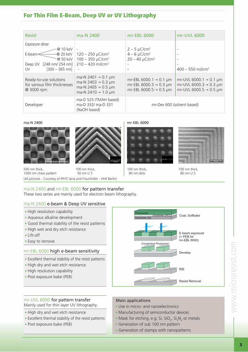
For Thin Film E-Beam, Deep UV or UV Lithography
Main applications • Use in micro- and nanoelectronics • Manufacturing of semiconductor devices • Mask for etching, e.g. Si, SiO2, Si3N4 or metals • Generation of sub 100 nm pattern • Generation of stamps with nanopatterns
500 nm thick,1000 nm chess pattern
100 nm thick, 50 nm L/ S
100 nm thick, 80 nm dots
100 nm thick, 80 nm L/ S
mr-EBL 6000
(All pictures - Courtesy of IPHT/ Jena and Fraunhofer - HHI/ Berlin)
Resist ma-N 2400 mr-EBL 6000 mr-UVL 6000
Exposure dose @ 10 keVE-beam @ 20 keV @ 50 keVDeep UV [248 nm/ 254 nm]UV [300 – 365 nm]
-120 – 250 µC/cm2
100 – 350 µC/cm2
210 – 420 mJ/cm2
-
2 – 5 µC/cm2
4 – 6 µC/cm2
20 – 40 µC/cm2
--
-- --400 – 550 mJ/cm2
Ready-to-use solutions for various film thicknesses @ 3000 rpm
ma-N 2401 g 0.1 µmma-N 2403 g 0.3 µmma-N 2405 g 0.5 µmma-N 2410 g 1.0 µm
mr-EBL 6000.1 g 0.1 µmmr-EBL 6000.3 g 0.3 µmmr-EBL 6000.5 g 0.5 µm
mr-UVL 6000.1 g 0.1 µmmr-UVL 6000.3 g 0.3 µmmr-UVL 6000.5 g 0.5 µm
Developerma-D 525 (TMAH based) ma-D 332/ ma-D 331 (NaOH based)
mr-Dev 600 (solvent based)
ma-N 2400 and mr-EBL 6000 for pattern transfer These two series are mainly used for electron beam lithography.
mr-UVL 6000 for pattern transferMainly used for thin layer UV lithography.
• High dry and wet etch resistance • Excellent thermal stability of the resist patterns• Post exposure bake (PEB)
ma-N 2400 e-beam & Deep UV sensitive
• High resolution capability • Aqueous alkaline development• Good thermal stability of the resist patterns• High wet and dry etch resistance• Lift-off• Easy to remove
mr-EBL 6000 high e-beam sensitivity
• Excellent thermal stability of the resist patterns • High dry and wet etch resistance• High resolution capability • Post exposure bake (PEB)
Photoresist
Substrate (Si)Substrate (SiO )2 Coat, Softbake
E-beam exposure(+ PEB formr-EBL 6000)
Develop
Crosslinked Photoresist
RIE
Resist Removal
ma-N 2400
3

Highly transparent Materials for Low Optical Loss and Standard Applications
50 µm thick
EpoCore
Resist EpoCore EpoClad
Spectral sensitivity Broadband, 365 nm
Ready-to-use solutionsfor various fi lm thicknesses from 1.5 µm to 120 µm
EpoCore 2 EpoCore 5 EpoCore 10 EpoCore 20 EpoCore 50
EpoClad 2 EpoClad 5 EpoClad 10 EpoClad 20 EpoClad 50
Developer mr-Dev 600 (solvent based)
Properties of cured resistShrinkage < 3 %
Thermal stability up to 230 °C
Refractive index @ 830 nm 1.58 1.57
Optical loss ~ 0.2 dB/cm @ 850 nm
Glass transition temperature
> 180 °C
Excellent stability after lamination
T > 185°C, pressure 23 kp/cm2 and refl ow tests 3 x 15 s @ 230 C°, TCT: 240 x -40 °C to 120 °C
EpoCore / EpoClad for preparation of polymer waveguides
Main applications
Singlemode (SM) and Multimode (MM) polymeric optical waveguides
100 µm thick
EpoClad
UV
EpoClad, fl ood exposedSubstrate
EpoCore
Patterning of EpoCore
EpoClad, fl ood exposure
Lamination
mr-DWL @ 405 nm for Direct Laser Writing (DLW)
Main applications • Fast and contactless prototyping by DLW • Optical applications in micro systems technology • Etch mask for wet and dry etch processes • Mould for electroplating • Mould for stamp fabrication/ template manufacture
50 µm thick 50 µm thick
Direct Laser Writing @ 405 nm
300 350 400 450 5000.0
0.2
0.4
0.6
Abso
rptio
n co
effic
ient
[µm
-1]
Wavelength [nm]
unexposed exposed exposed and post exposure baked
Resist mr-DWL
Spectral sensitivityHigh sensitivity > 400 nmDLW @ 405 nm
Ready-to-use solutions for various fi lm thicknesses
mr-DWL 5: 3 µm g 12 µmmr-DWL 40: 20 µm g 100 µmmr-DWL 100: 20 µm g 150 µm
Developer mr-Dev 600 (solvent based)
N
egat
ive
Phot
ores
ists
© micro resist technology GmbH | November 2017
4
w
ww
.micr
ores
ist.c
om