draft cs5343/4 3/10/15 - d3uzseaevmutz1.cloudfront.net · ers, a/v receivers, and automotive...
TRANSCRIPT
CS5343/4Draft3/10/15
98 dB, 96 kHz, Multi-Bit Audio A/D Converter
Features
Advanced Multi-Bit Architecture
24-bit Conversion
Supports Audio Sample Rates Up to 108 kHz
98 dB Dynamic Range at 5 V
-92 dB THD+N at 5 V
Low-Latency Digital Filter
High-Pass Filter to Remove DC Offsets
Single +3.3 V or +5 V Power Supply
Power Consumption < 40 mW at 3.3 V
Master or Slave Operation
Slave Mode Speed Auto-Detect
Master Mode Default Settings
256x or 384x MCLK/LRCK Ratio
CS5343 Supports I²S Audio Format
CS5344 Supports Left-Justified Audio Format
General Description
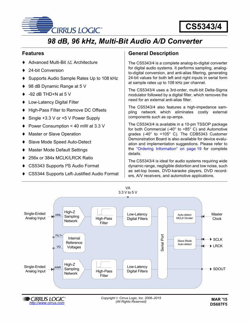
The CS5343/4 is a complete analog-to-digital converterfor digital audio systems. It performs sampling, analog-to-digital conversion, and anti-alias filtering, generating24-bit values for both left and right inputs in serial format sample rates up to 108 kHz per channel.
The CS5343/4 uses a 3rd-order, multi-bit Delta-Sigmamodulator followed by a digital filter, which removes theneed for an external anti-alias filter.
The CS5343/4 also features a high-impedance sam-pling network which eliminates costly externalcomponents such as op-amps.
The CS5343/4 is available in a 10-pin TSSOP packagefor both Commercial (-40° to +85° C) and Automotivegrades (-40° to +105° C). The CDB5343 CustomerDemonstration Board is also available for device evalu-ation and implementation suggestions. Please refer tothe “Ordering Information” on page 19 for completedetails.
The CS5343/4 is ideal for audio systems requiring widedynamic range, negligible distortion and low noise, suchas set-top boxes, DVD-karaoke players, DVD record-ers, A/V receivers, and automotive applications.
High-Pass Filter
High-Pass Filter
Low-Latency Digital Filters
VA3.3 V to 5 V
Internal Reference Voltages
High-Z Sampling Network
Auto-detect MCLK Divider
Master Clock
Single-Ended Analog Input
Low-Latency Digital Filters
High-Z Sampling Network
Single-Ended Analog Input
SCLK
LRCK
SDOUT
FILT+
VQ
AINR
AINL
Se
rial P
ort
Slave Mode Auto-detect
High-Pass Filter
Copyright Cirrus Logic, Inc. 2006–2015(All Rights Reserved)http://www.cirrus.com
MAR '15DS687F5
CS5343/4Draft
3/10/15
TABLE OF CONTENTS1. PIN DESCRIPTIONS .............................................................................................................................. 32. CHARACTERISTICS AND SPECIFICATIONS ...................................................................................... 4
RECOMMENDED OPERATING CONDITIONS ..................................................................................... 4ABSOLUTE MAXIMUM RATINGS ......................................................................................................... 4ANALOG CHARACTERISTICS - COMMERCIAL GRADE (-CZZ) ......................................................... 5ANALOG CHARACTERISTICS - AUTOMOTIVE GRADE (-DZZ) ......................................................... 6DIGITAL FILTER CHARACTERISTICS ................................................................................................ 7DC ELECTRICAL CHARACTERISTICS ................................................................................................ 7DIGITAL CHARACTERISTICS ............................................................................................................... 8SYSTEM CLOCKING AND SERIAL AUDIO INTERFACE ..................................................................... 9
3. TYPICAL CONNECTION DIAGRAM ................................................................................................... 114. APPLICATIONS ................................................................................................................................... 12
4.1 Operation as Clock Master or Slave ............................................................................................... 124.1.1 Slave Mode Operation ........................................................................................................... 124.1.2 Master Mode Operation ......................................................................................................... 13
4.1.2.1 Master Mode Speed Selection ................................................................................... 134.1.3 Master Clock ......................................................................................................................... 13
4.2 Serial Audio Interface ..................................................................................................................... 144.3 Digital Interface ............................................................................................................................... 144.4 Analog Connections ....................................................................................................................... 14
4.4.1 Component Values ................................................................................................................ 154.5 Grounding and Power Supply Decoupling ...................................................................................... 154.6 Synchronization of Multiple Devices ............................................................................................... 16
5. FILTER PLOTS - ALL SPEED MODES ............................................................................................... 166. PARAMETER DEFINITIONS ................................................................................................................ 177. PACKAGE DIMENSIONS .................................................................................................................... 18
THERMAL CHARACTERISTICS .......................................................................................................... 188. ORDERING INFORMATION ................................................................................................................ 199. REVISION HISTORY ............................................................................................................................ 20
2 DS687F5
CS5343/4Draft
3/10/15
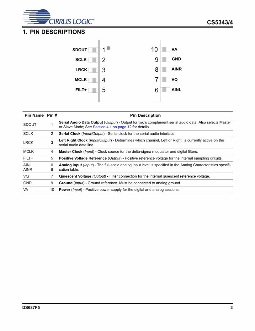
1. PIN DESCRIPTIONS
Pin Name Pin # Pin Description
SDOUT 1Serial Audio Data Output (Output) - Output for two’s complement serial audio data. Also selects Master or Slave Mode; See Section 4.1 on page 12 for details.
SCLK 2 Serial Clock (Input/Output) - Serial clock for the serial audio interface.
LRCK 3Left Right Clock (Input/Output) - Determines which channel, Left or Right, is currently active on the serial audio data line.
MCLK 4 Master Clock (Input) - Clock source for the delta-sigma modulator and digital filters.
FILT+ 5 Positive Voltage Reference (Output) - Positive reference voltage for the internal sampling circuits.
AINLAINR
68
Analog Input (Input) - The full-scale analog input level is specified in the Analog Characteristics specifi-cation table.
VQ 7 Quiescent Voltage (Output) - Filter connection for the internal quiescent reference voltage.
GND 9 Ground (Input) - Ground reference. Must be connected to analog ground.
VA 10 Power (Input) - Positive power supply for the digital and analog sections.
1
2
3
4
5 6
7
8
9
10SDOUT
SCLK
LRCK
MCLK
FILT+
VA
GND
AINR
VQ
AINL
DS687F5 3
CS5343/4Draft
3/10/15
2. CHARACTERISTICS AND SPECIFICATIONS
RECOMMENDED OPERATING CONDITIONSGND = 0 V, all voltages with respect to GND.
ABSOLUTE MAXIMUM RATINGSGND = 0 V, all voltages with respect to GND. (Note 1)
Notes:
1. Operation beyond these limits may result in permanent damage to the device. Normal operation is notguaranteed at these extremes.
2. Any pin except supplies. Transient currents of up to ±100 mA on the analog input pins will not causeSCR latch-up.
3. The maximum over/under voltage is limited by the input current.
Parameter Symbol Min Typ Max Unit
Power SuppliesVA
3.14.75
3.35.0
3.55.25
VV
Ambient Operating Temperature Commercial (-CZZ)Automotive (-DZZ)
TACTAD
-40-40
--
85105
°C°C
Parameter Symbol Min Max Unit
DC Power Supplies VA -0.3 +6.0 V
Input Current (Note 2) Iin -10 10 mA
Input Voltage (Note 3) VIN -0.7 VA+0.7 V
Ambient Operating Temperature (Power Applied) TA -50 +115 C
Storage Temperature Tstg -65 +150 C
4 DS687F5
CS5343/4Draft
3/10/15
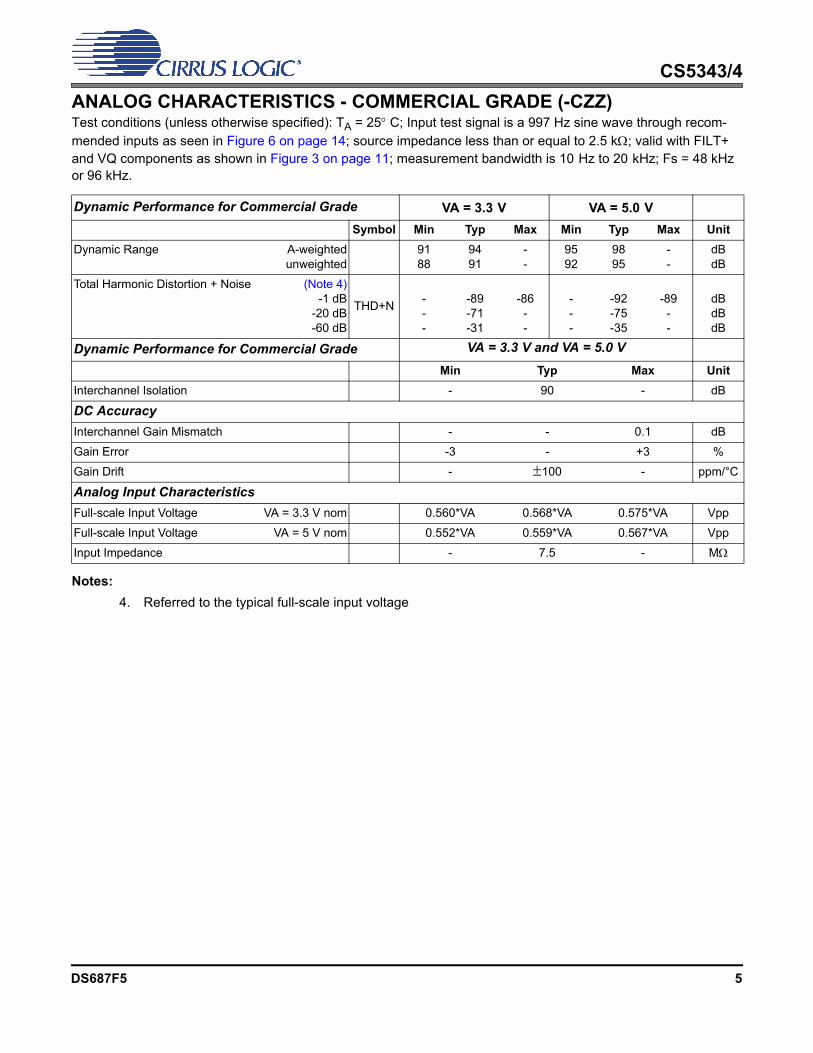
ANALOG CHARACTERISTICS - COMMERCIAL GRADE (-CZZ)Test conditions (unless otherwise specified): TA = 25C; Input test signal is a 997 Hz sine wave through recom-mended inputs as seen in Figure 6 on page 14; source impedance less than or equal to 2.5 k; valid with FILT+ and VQ components as shown in Figure 3 on page 11; measurement bandwidth is 10 Hz to 20 kHz; Fs = 48 kHz or 96 kHz.
Notes:
4. Referred to the typical full-scale input voltage
Dynamic Performance for Commercial Grade VA = 3.3 V VA = 5.0 V
Symbol Min Typ Max Min Typ Max Unit
Dynamic Range A-weightedunweighted
9188
9491
--
9592
9895
--
dBdB
Total Harmonic Distortion + Noise (Note 4) -1 dB-20 dB-60 dB
THD+N---
-89-71-31
-86--
---
-92-75-35
-89--
dBdBdB
Dynamic Performance for Commercial Grade VA = 3.3 V and VA = 5.0 V
Min Typ Max Unit
Interchannel Isolation - 90 - dB
DC Accuracy
Interchannel Gain Mismatch - - 0.1 dB
Gain Error -3 - +3 %
Gain Drift - 100 - ppm/°C
Analog Input Characteristics
Full-scale Input Voltage VA = 3.3 V nom 0.560*VA 0.568*VA 0.575*VA Vpp
Full-scale Input Voltage VA = 5 V nom 0.552*VA 0.559*VA 0.567*VA Vpp
Input Impedance - 7.5 - M
DS687F5 5
CS5343/4Draft
3/10/15
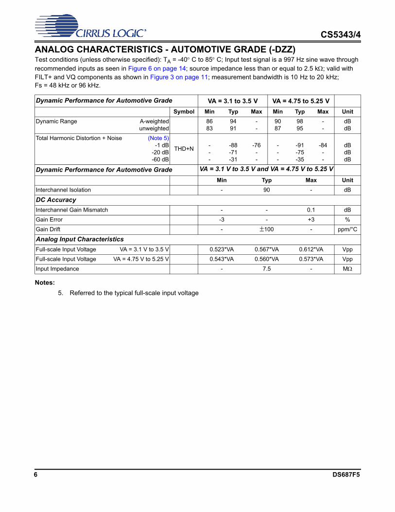
ANALOG CHARACTERISTICS - AUTOMOTIVE GRADE (-DZZ)Test conditions (unless otherwise specified): TA = -40C to 85C; Input test signal is a 997 Hz sine wave through recommended inputs as seen in Figure 6 on page 14; source impedance less than or equal to 2.5 k; valid with FILT+ and VQ components as shown in Figure 3 on page 11; measurement bandwidth is 10 Hz to 20 kHz; Fs = 48 kHz or 96 kHz.
Notes:
5. Referred to the typical full-scale input voltage
Dynamic Performance for Automotive Grade VA = 3.1 to 3.5 V VA = 4.75 to 5.25 V
Symbol Min Typ Max Min Typ Max Unit
Dynamic Range A-weightedunweighted
8683
9491
--
9087
9895
--
dBdB
Total Harmonic Distortion + Noise (Note 5) -1 dB
-20 dB-60 dB
THD+N---
-88-71-31
-76--
---
-91-75-35
-84--
dBdBdB
Dynamic Performance for Automotive Grade VA = 3.1 V to 3.5 V and VA = 4.75 V to 5.25 V
Min Typ Max Unit
Interchannel Isolation - 90 - dB
DC Accuracy
Interchannel Gain Mismatch - - 0.1 dB
Gain Error -3 - +3 %
Gain Drift - 100 - ppm/°C
Analog Input Characteristics
Full-scale Input Voltage VA = 3.1 V to 3.5 V 0.523*VA 0.567*VA 0.612*VA Vpp
Full-scale Input Voltage VA = 4.75 V to 5.25 V 0.543*VA 0.560*VA 0.573*VA Vpp
Input Impedance - 7.5 - M
6 DS687F5
CS5343/4Draft
3/10/15
DIGITAL FILTER CHARACTERISTICS
Notes:
6. Response shown is for Fs equal to 48 kHz. Filter characteristics scale with Fs.
DC ELECTRICAL CHARACTERISTICSGND = 0 V, all voltages with respect to 0 V. MCLK=12.288 MHz; Master Mode.
Notes:
7. Device enters power-down mode when MCLK is held static.
8. Valid with the recommended capacitor values on FILT+ and VQ as shown in the Typical ConnectionDiagram.
Parameter Symbol Min Typ Max Unit
All Speed Modes
Passband (-0.1 dB) 0 - 0.489 Fs
Passband Ripple -0.031 - 0.031 dB
Stopband 0.560 - - Fs
Stopband Attenuation 60 - - dB
Total Group Delay (Fs = Output Sample Rate) tgd - 12/Fs - s
High-Pass Filter Characteristics
Frequency Response -3.0 dB-0.13 dB (Note 6)
- 120
--
HzHz
Phase Deviation @ 20 Hz (Note 6) - 10 - Deg
Passband Ripple - - 0 dB
Parameter Symbol
VA = 3.3 V VA = 5.0 V
Min Typ Max Min Typ Max Unit
Power Supply Current (Normal Operation) IA - 11 15 - 12 17 mA
Power Supply Current (Power-Down Mode) (Note 7) IA - 10 - - 40 - uA
Power Consumption (Normal Operation)(Power-Down Mode) (Note 7)
--
--
36<1
50-
--
60<1
85-
mWmW
Parameter Symbol Min Typ Max Unit
Power Supply Rejection Ratio (1 kHz) (Note 8) PSRR - 65 - dB
VQ Nominal Voltage
Output Impedance
--
0.44xVA25
--
Vk
Filt+ Nominal VoltageOutput ImpedanceMaximum allowable DC current source/sink
---
VA2202.5
---
VkuA
DS687F5 7
CS5343/4Draft
3/10/15
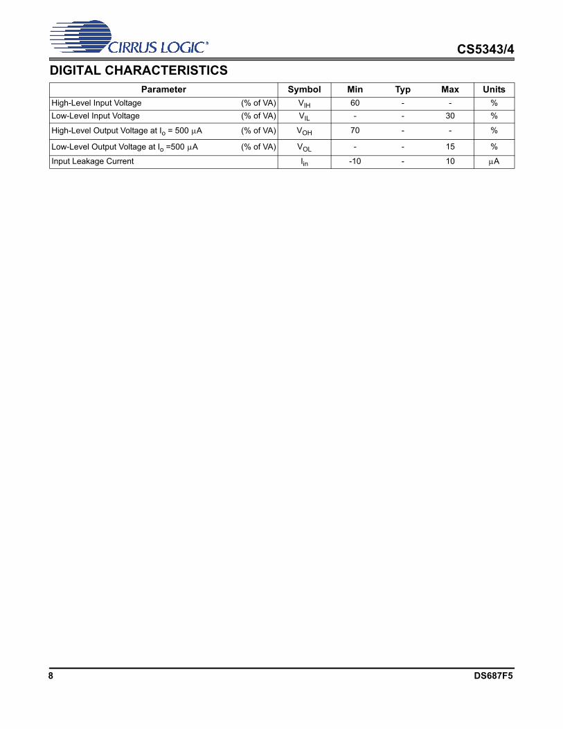
DIGITAL CHARACTERISTICSParameter Symbol Min Typ Max Units
High-Level Input Voltage (% of VA) VIH 60 - - %
Low-Level Input Voltage (% of VA) VIL - - 30 %
High-Level Output Voltage at Io = 500 A (% of VA) VOH 70 - - %
Low-Level Output Voltage at Io =500 A (% of VA) VOL - - 15 %
Input Leakage Current Iin -10 - 10 A
8 DS687F5
CS5343/4Draft
3/10/15
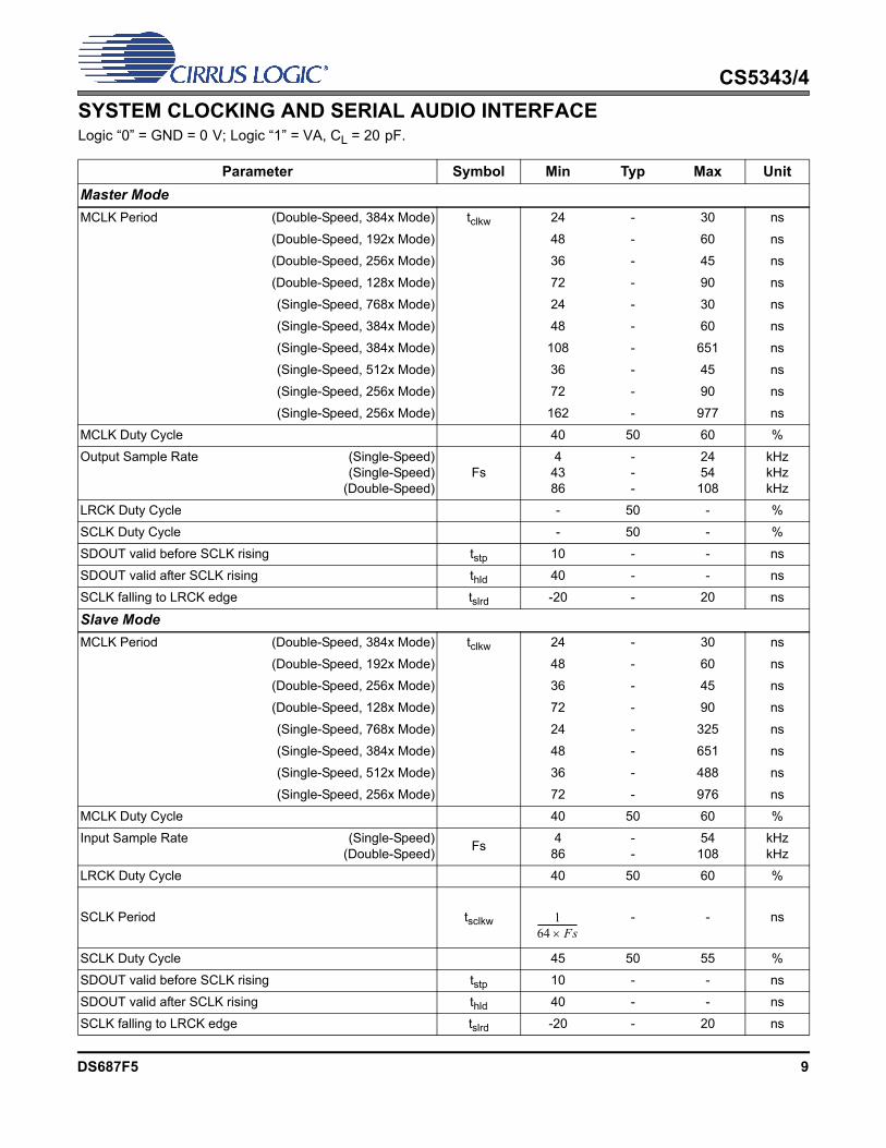
SYSTEM CLOCKING AND SERIAL AUDIO INTERFACELogic “0” = GND = 0 V; Logic “1” = VA, CL = 20 pF.
Parameter Symbol Min Typ Max Unit
Master Mode
MCLK Period (Double-Speed, 384x Mode) tclkw 24 - 30 ns
(Double-Speed, 192x Mode) 48 - 60 ns
(Double-Speed, 256x Mode) 36 - 45 ns
(Double-Speed, 128x Mode) 72 - 90 ns
(Single-Speed, 768x Mode) 24 - 30 ns
(Single-Speed, 384x Mode) 48 - 60 ns
(Single-Speed, 384x Mode) 108 - 651 ns
(Single-Speed, 512x Mode) 36 - 45 ns
(Single-Speed, 256x Mode) 72 - 90 ns
(Single-Speed, 256x Mode) 162 - 977 ns
MCLK Duty Cycle 40 50 60 %
Output Sample Rate (Single-Speed)(Single-Speed)
(Double-Speed)Fs
44386
---
2454
108
kHzkHzkHz
LRCK Duty Cycle - 50 - %
SCLK Duty Cycle - 50 - %
SDOUT valid before SCLK rising tstp 10 - - ns
SDOUT valid after SCLK rising thld 40 - - ns
SCLK falling to LRCK edge tslrd -20 - 20 ns
Slave Mode
MCLK Period (Double-Speed, 384x Mode) tclkw 24 - 30 ns
(Double-Speed, 192x Mode) 48 - 60 ns
(Double-Speed, 256x Mode) 36 - 45 ns
(Double-Speed, 128x Mode) 72 - 90 ns
(Single-Speed, 768x Mode) 24 - 325 ns
(Single-Speed, 384x Mode) 48 - 651 ns
(Single-Speed, 512x Mode) 36 - 488 ns
(Single-Speed, 256x Mode) 72 - 976 ns
MCLK Duty Cycle 40 50 60 %
Input Sample Rate (Single-Speed)(Double-Speed)
Fs4
86--
54108
kHzkHz
LRCK Duty Cycle 40 50 60 %
SCLK Period tsclkw - - ns
SCLK Duty Cycle 45 50 55 %
SDOUT valid before SCLK rising tstp 10 - - ns
SDOUT valid after SCLK rising thld 40 - - ns
SCLK falling to LRCK edge tslrd -20 - 20 ns
164 Fs------------------
DS687F5 9
CS5343/4Draft
3/10/15
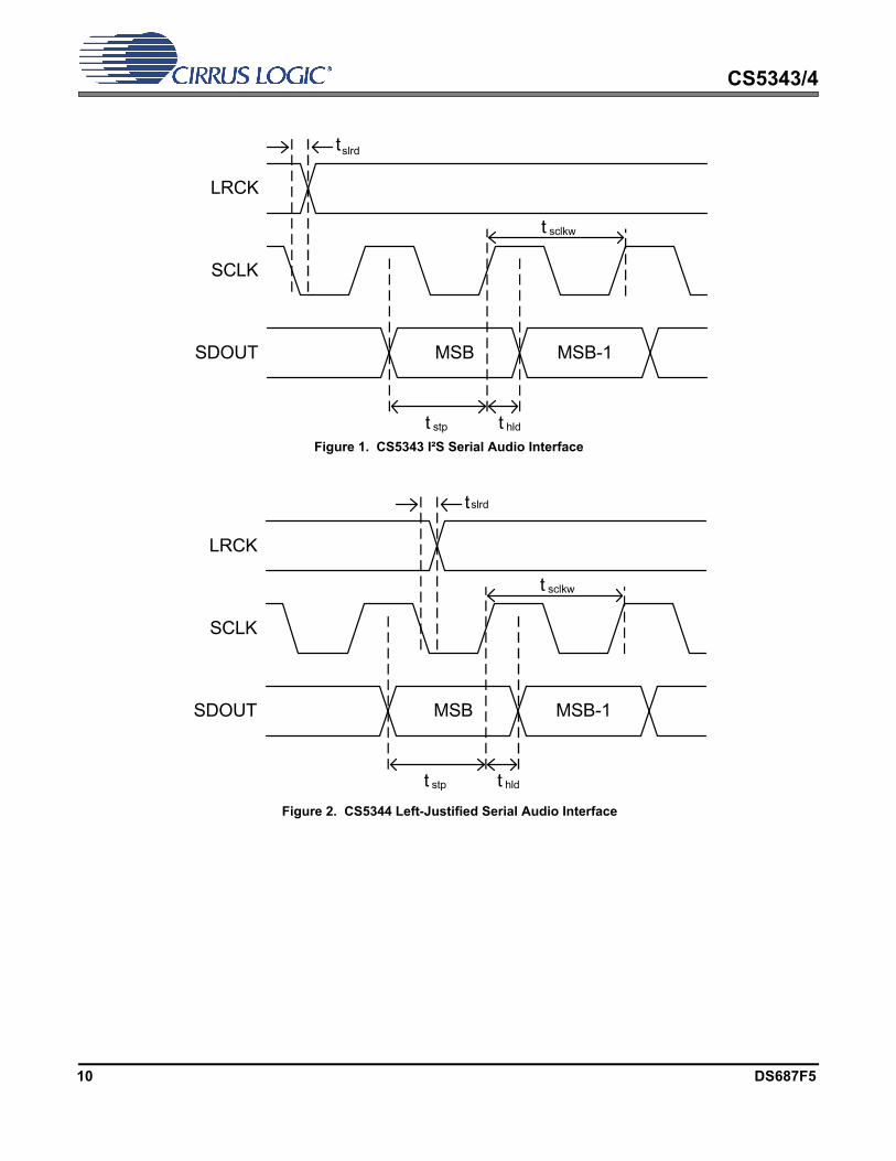
Figure 1. CS5343 I²S Serial Audio Interface
t tstp hld
MSB MSB-1
LRCK
SCLK
SDOUT
tslrd
t sclkw
Figure 2. CS5344 Left-Justified Serial Audio Interface
t tstp hld
MSB MSB-1
LRCK
SCLK
SDOUT
tslrd
t sclkw
10 DS687F5
CS5343/4Draft
3/10/15
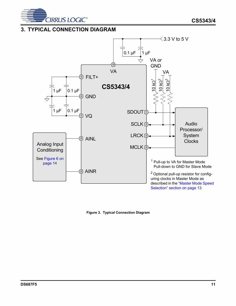
3. TYPICAL CONNECTION DIAGRAM
Figure 3. Typical Connection Diagram
AINL
AINR
6
8
1SDOUT
9 GND
7 VQ
VA
10
5 FILT+
2SCLK
3LRCK
4MCLK
Audio Processor/
System Clocks
VA or GND
VA
3.3 V to 5 V
CS5343/4
10
k1
10
k2
Analog Input Conditioning
10
k2
1 µF 0.1 µF
1 µF 0.1 µF
1 µF0.1 µF
See Figure 6 on page 14
1 Pull-up to VA for Master ModePull-down to GND for Slave Mode
2 Optional pull-up resistor for config-uring clocks in Master Mode as described in the “Master Mode Speed Selection” section on page 13
DS687F5 11
CS5343/4Draft
3/10/15
4. APPLICATIONS
4.1 Operation as Clock Master or Slave
The CS5343/4 supports operation as either a clock master or slave. As a clock master, the left/right andserial clocks are synchronously generated on-chip and output on the LRCK and SCLK pins, respectively.As a clock slave, the LRCK and SCLK pins are always inputs and require external generation of the left/rightand serial clocks. The selection of clock master or slave is made via a 10 k pull-up resistor from SDOUTto VA for Master Mode selection or via a 10 kpull-down resistor from SDOUT to GND for Slave Mode se-lection, as shown in Table 1.
4.1.1 Slave Mode Operation
A unique feature of the CS5343/4 is the automatic selection of either Single- or Double-Speed Mode whenacting as a clock slave. The auto-mode selection feature supports all standard audio sample rates from4 to 108 kHz. Please refer to Table 2 for supported sample rate ranges in Slave Mode.
Table 2. Speed Modes and the Associated Sample Rates (Fs) in Slave Mode
Mode Selection
Master Mode 10 k pull-up resistor from SDOUT to VA
Slave Mode 10 kpull-down resistor from SDOUT to GND
Table 1. Master/Slave Mode Selection
Speed ModeMCLK/LRCK
RatioSCLK/LRCK
RatioInput Sample Rate Range (kHz)
Single-Speed Mode
256x 64 4 - 54
512x 64 4 - 54
384x 48, 64 4 - 54
768x 48, 64 4 - 54
Double-Speed Mode
128x 64 86 - 108
256x 64 86 - 108
192x 48, 64 86 - 108
384x 48, 64 86 - 108
12 DS687F5
CS5343/4Draft
3/10/15
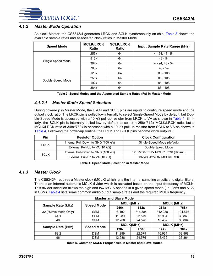
4.1.2 Master Mode Operation
As clock Master, the CS5343/4 generates LRCK and SCLK synchronously on-chip. Table 3 shows theavailable sample rates and associated clock ratios in Master Mode.
4.1.2.1 Master Mode Speed Selection
During power-up in Master Mode, the LRCK and SCLK pins are inputs to configure speed mode and theoutput clock ratio. The LRCK pin is pulled low internally to select Single-Speed Mode by default, but Dou-ble-Speed Mode is accessed with a 10 k pull-up resistor from LRCK to VA as shown in Table 4. Simi-larly, the SCLK pin is internally pulled-low by default to select a 256x/512x MCLK/LRCK ratio, but aMCLK/LRCK ratio of 348x/768x is accessed with a 10 k pull-up resistor from SCLK to VA as shown inTable 4. Following the power-up routine, the LRCK and SCLK pins become clock outputs.
4.1.3 Master Clock
The CS5343/4 requires a Master clock (MCLK) which runs the internal sampling circuits and digital filters.There is an internal automatic MCLK divider which is activated based on the input frequency of MCLK.This divider selection allows the high and low MCLK speeds in a given speed mode (i.e. 256x and 512xin SSM). Table 4 lists some common audio output sample rates and the required MCLK frequency.
Speed ModeMCLK/LRCK
RatioSCLK/LRCK
RatioInput Sample Rate Range (kHz)
Single-Speed Mode
256x 64 4 - 24, 43 - 54
512x 64 43 - 54
384x 64 4 - 24, 43 - 54
768x 64 43 - 54
Double-Speed Mode
128x 64 86 - 108
256x 64 86 - 108
192x 64 86 - 108
384x 64 86 - 108
Table 3. Speed Modes and the Associated Sample Rates (Fs) in Master Mode
Pin Resistor Option Clock Configuration
LRCKInternal Pull-Down to GND (100 k) Single-Speed Mode (default)
External Pull-Up to VA (10 k) Double-Speed Mode
SCLKInternal Pull-Down to GND (100 k) 128x/256x/512x MCLK/LRCK (default)
External Pull-Up to VA (10 k) 192x/384x/768x MCLK/LRCK
Table 4. Speed Mode Selection in Master Mode
Master and Slave Mode
Sample Rate (kHz) Speed ModeMCLK(MHz) MCLK (MHz)
256x 512x 384x 768x32 (*Slave Mode Only) SSM *8.192 *16.384 *12.288 *24.576
44.1 SSM 11.289 22.579 16.934 33.86848 SSM 12.288 24.576 18.432 36.864
Sample Rate (kHz) Speed ModeMCLK(MHz) MCLK (MHz)
128x 256x 192x 384x88.2 DSM 11.289 22.579 16.934 33.86896 DSM 12.288 24.576 18.432 36.864
Table 5. Common MCLK Frequencies in Master and Slave Modes
DS687F5 13
CS5343/4Draft
3/10/15
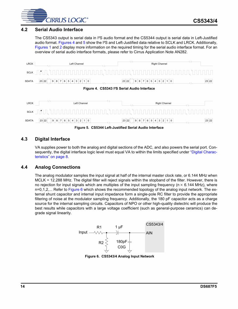
4.2 Serial Audio Interface
The CS5343 output is serial data in I²S audio format and the CS5344 output is serial data in Left-Justifiedaudio format. Figures 4 and 5 show the I²S and Left-Justified data relative to SCLK and LRCK. Additionally,Figures 1 and 2 display more information on the required timing for the serial audio interface format. For anoverview of serial audio interface formats, please refer to Cirrus Application Note AN282.
4.3 Digital Interface
VA supplies power to both the analog and digital sections of the ADC, and also powers the serial port. Con-sequently, the digital interface logic level must equal VA to within the limits specified under “Digital Charac-teristics” on page 8.
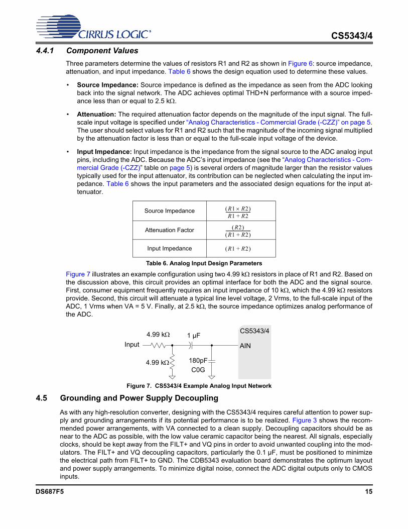
4.4 Analog Connections
The analog modulator samples the input signal at half of the internal master clock rate, or 6.144 MHz whenMCLK = 12.288 MHz. The digital filter will reject signals within the stopband of the filter. However, there isno rejection for input signals which are multiples of the input sampling frequency (n 6.144 MHz), wheren=0,1,2,... Refer to Figure 6 which shows the recommended topology of the analog input network. The ex-ternal shunt capacitor and internal input impedance form a single-pole RC filter to provide the appropriatefiltering of noise at the modulator sampling frequency. Additionally, the 180 pF capacitor acts as a chargesource for the internal sampling circuits. Capacitors of NPO or other high-quality dielectric will produce thebest results while capacitors with a large voltage coefficient (such as general-purpose ceramics) can de-grade signal linearity.
Figure 4. CS5343 I²S Serial Audio Interface
SDATA 23 22 8 7 23 22
SCLK
LRCK
23 226 5 4 3 2 1 0 8 7 6 5 4 3 2 1 09 9
Left Channel Right Channel
Figure 5. CS5344 Left-Justified Serial Audio Interface
SDATA 23 22 7 6 23 22
SCLK
LRCK
23 225 4 3 2 1 08 7 6 5 4 3 2 1 089 9
Left Channel Right Channel
Figure 6. CS5343/4 Analog Input Network
CS5343/4
AINInputR1
R2
1 µF
180pF
C0G
14 DS687F5
CS5343/4Draft
3/10/15
4.4.1 Component Values
Three parameters determine the values of resistors R1 and R2 as shown in Figure 6: source impedance,attenuation, and input impedance. Table 6 shows the design equation used to determine these values.
• Source Impedance: Source impedance is defined as the impedance as seen from the ADC lookingback into the signal network. The ADC achieves optimal THD+N performance with a source imped-ance less than or equal to 2.5 k.
• Attenuation: The required attenuation factor depends on the magnitude of the input signal. The full-scale input voltage is specified under “Analog Characteristics - Commercial Grade (-CZZ)” on page 5.The user should select values for R1 and R2 such that the magnitude of the incoming signal multipliedby the attenuation factor is less than or equal to the full-scale input voltage of the device.
• Input Impedance: Input impedance is the impedance from the signal source to the ADC analog inputpins, including the ADC. Because the ADC’s input impedance (see the “Analog Characteristics - Com-mercial Grade (-CZZ)” table on page 5) is several orders of magnitude larger than the resistor valuestypically used for the input attenuator, its contribution can be neglected when calculating the input im-pedance. Table 6 shows the input parameters and the associated design equations for the input at-tenuator.
Figure 7 illustrates an example configuration using two 4.99 kresistors in place of R1 and R2. Based onthe discussion above, this circuit provides an optimal interface for both the ADC and the signal source.First, consumer equipment frequently requires an input impedance of 10 kwhich the 4.99 kresistorsprovide. Second, this circuit will attenuate a typical line level voltage, 2 Vrms, to the full-scale input of theADC, 1 Vrms when VA = 5 V. Finally, at 2.5 kthe source impedance optimizes analog performance ofthe ADC.
4.5 Grounding and Power Supply Decoupling
As with any high-resolution converter, designing with the CS5343/4 requires careful attention to power sup-ply and grounding arrangements if its potential performance is to be realized. Figure 3 shows the recom-mended power arrangements, with VA connected to a clean supply. Decoupling capacitors should be asnear to the ADC as possible, with the low value ceramic capacitor being the nearest. All signals, especiallyclocks, should be kept away from the FILT+ and VQ pins in order to avoid unwanted coupling into the mod-ulators. The FILT+ and VQ decoupling capacitors, particularly the 0.1 µF, must be positioned to minimizethe electrical path from FILT+ to GND. The CDB5343 evaluation board demonstrates the optimum layoutand power supply arrangements. To minimize digital noise, connect the ADC digital outputs only to CMOSinputs.
Source Impedance
Attenuation Factor
Input Impedance
Table 6. Analog Input Design Parameters
R1 R2 R1 R2+-------------------------
R2 R1 R2+ -------------------------
R1 R2+
Figure 7. CS5343/4 Example Analog Input Network
CS5343/4
AINInput
4.99 k
4.99 k
1 µF
180pF
C0G
DS687F5 15
CS5343/4Draft
3/10/15
4.6 Synchronization of Multiple Devices
In systems where multiple ADCs are required, care must be taken to achieve simultaneous sampling. Toensure synchronous sampling, the MCLK, SCLK, and LRCK signals must be the same for all of the CS5343and CS5344 devices in the system.
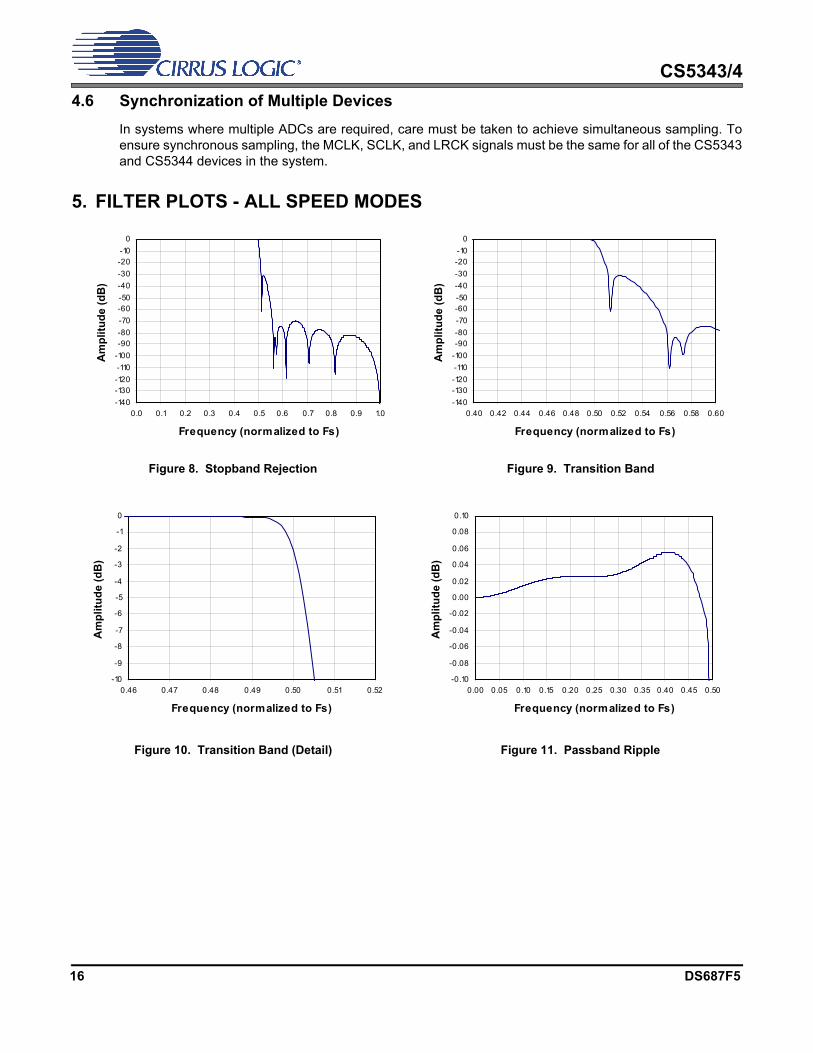
5. FILTER PLOTS - ALL SPEED MODES
Figure 8. Stopband Rejection Figure 9. Transition Band
-140
-130-120
-110
-100
-90-80
-70
-60-50
-40
-30
-20-10
0
0.0 0.1 0.2 0.3 0.4 0.5 0.6 0.7 0.8 0.9 1.0
Frequency (normalized to Fs)
Am
plit
ud
e (d
B)
-140
-130-120
-110
-100
-90-80
-70
-60-50
-40
-30
-20-10
0
0.40 0.42 0.44 0.46 0.48 0.50 0.52 0.54 0.56 0.58 0.60
Frequency (normalized to Fs)A
mp
litu
de
(dB
)
Figure 10. Transition Band (Detail) Figure 11. Passband Ripple
-0.10
-0.08
-0.06
-0.04
-0.02
0.00
0.02
0.04
0.06
0.08
0.10
0.00 0.05 0.10 0.15 0.20 0.25 0.30 0.35 0.40 0.45 0.50
Frequency (normalized to Fs)
Am
plit
ud
e (d
B)
-10
-9
-8
-7
-6
-5
-4
-3
-2
-1
0
0.46 0.47 0.48 0.49 0.50 0.51 0.52
Frequency (normalized to Fs)
Am
plit
ud
e (d
B)
16 DS687F5
CS5343/4Draft
3/10/15
6. PARAMETER DEFINITIONS
Dynamic Range
The ratio of the rms value of the signal to the rms sum of all other spectral components over the specifiedbandwidth. Dynamic Range is a signal-to-noise ratio measurement over the specified bandwidth made witha -60 dBFS signal. 60 dB is added to resulting measurement to refer the measurement to full-scale. Thistechnique ensures that the distortion components are below the noise level and do not affect the measure-ment. This measurement technique has been accepted by the Audio Engineering Society, AES17-1991,and the Electronic Industries Association of Japan, EIAJ CP-307. Expressed in decibels.
Total Harmonic Distortion + Noise
The ratio of the rms value of the signal to the rms sum of all other spectral components over the specifiedbandwidth (typically 10 Hz to 20 kHz), including distortion components. Expressed in decibels. Measuredat -1 and -20 dBFS as suggested in AES17-1991 Annex A.
Frequency Response
A measure of the amplitude response variation from 10 Hz to 20 kHz relative to the amplitude response at1 kHz. Units in decibels.
Interchannel Isolation
A measure of crosstalk between the left and right channels. Measured for each channel at the converter'soutput with no signal to the input under test and a full-scale signal applied to the other channel. Units in deci-bels.
Interchannel Gain Mismatch
The gain difference between left and right channels. Units in decibels.
Gain Error
The deviation from the nominal full-scale analog input for a full-scale digital output.
Gain Drift
The change in gain value with temperature. Units in ppm/°C.
DS687F5 17

CS5343/4Draft
3/10/15
7. PACKAGE DIMENSIONS
Notes:
1. Reference document: JEDEC MO-187
2. D does not include mold flash or protrusions, which is 0.15 mm max. per side.
3. E1 does not include inter-lead flash or protrusions, which is 0.15 mm max per side.
4. Dimension b does not include a total allowable dambar protrusion of 0.08 mm max.
5. Exceptions to JEDEC dimension.
THERMAL CHARACTERISTICS
INCHES MILLIMETERS NOTE
DIM MIN NOM MAX MIN NOM MAXA -- -- 0.0433 -- -- 1.10
A1 0 -- 0.0059 0 -- 0.15
A2 0.0295 -- 0.0374 0.75 -- 0.95
b 0.0059 -- 0.0118 0.15 -- 0.30 4, 5
c 0.0031 -- 0.0091 0.08 -- 0.23
D -- 0.1181 BSC -- -- 3.00 BSC -- 2
E -- 0.1929 BSC -- -- 4.90 BSC --
E1 -- 0.1181 BSC -- -- 3.00 BSC -- 3
e -- 0.0197 BSC -- -- 0.50 BSC --
L 0.0157 0.0236 0.0315 0.40 0.60 0.80
L1 -- 0.0374 REF -- -- 0.95 REF --
µ 0° -- 8° 0° -- 8°
Controlling Dimension is Millimeters
Parameter Symbol Min Typ Max Unit
Allowable Junction Temperature TJ - - 135 CJunction to Ambient Thermal Impedance
(4-layer PCB)(2-layer PCB)
JA-4JA-2
--
100170
--
C/WC/W
10LD TSSOP (3 mm BODY) PACKAGE DRAWING (Note 1)
E
N
1 2 3
e bA1
A2 A
D
SEATINGPLANE
E11
L
SIDE VIEW
END VIEW
TOP VIEW
L1
c
18 DS687F5
CS5343/4Draft
3/10/15
8. ORDERING INFORMATION
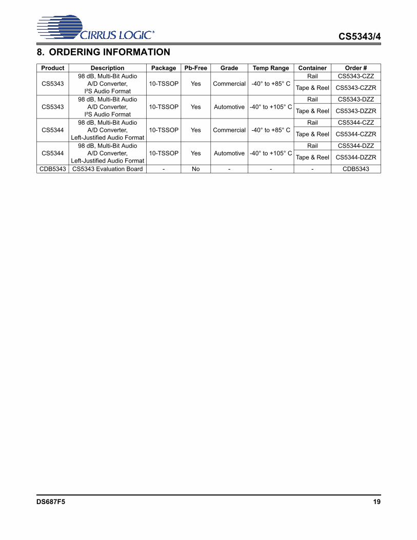
Product Description Package Pb-Free Grade Temp Range Container Order #
CS534398 dB, Multi-Bit Audio
A/D Converter, I²S Audio Format
10-TSSOP Yes Commercial -40° to +85° CRail CS5343-CZZ
Tape & Reel CS5343-CZZR
CS534398 dB, Multi-Bit Audio
A/D Converter, I²S Audio Format
10-TSSOP Yes Automotive -40° to +105° CRail CS5343-DZZ
Tape & Reel CS5343-DZZR
CS534498 dB, Multi-Bit Audio
A/D Converter, Left-Justified Audio Format
10-TSSOP Yes Commercial -40° to +85° CRail CS5344-CZZ
Tape & Reel CS5344-CZZR
CS534498 dB, Multi-Bit Audio
A/D Converter, Left-Justified Audio Format
10-TSSOP Yes Automotive -40° to +105° CRail CS5344-DZZ
Tape & Reel CS5344-DZZR
CDB5343 CS5343 Evaluation Board - No - - - CDB5343
DS687F5 19
CS5343/4Draft
3/10/15
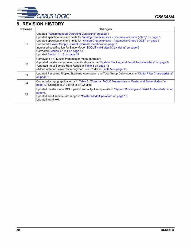
9. REVISION HISTORYRelease Changes
F1
Updated “Recommended Operating Conditions” on page 4Updated specifications and limits for “Analog Characteristics - Commercial Grade (-CZZ)” on page 5Updated specifications and limits for “Analog Characteristics - Automotive Grade (-DZZ)” on page 6Corrected “Power Supply Current (Normal Operation)” on page 7Increased specification for Slave-Mode “SDOUT valid after SCLK rising” on page 9Corrected Section 4.1.2.1 on page 13Updated Section 4.1.3 on page 13
F2
Removed Fs < 43 kHz from master mode operation:-Updated master mode timing specifications in the “System Clocking and Serial Audio Interface” on page 9-Updated Input Sample Rate Range in Table 3 on page 13-Added note for “slave mode only” for Fs = 32 kHz in Table 5 on page 13.
F3Updated Passband Ripple, Stopband Attenuation and Total Group Delay specs in “Digital Filter Characteristics” on page 7.
F4Corrected a typographical error in Table 5, “Common MCLK Frequencies in Master and Slave Modes,” on page 13. Changed 8.912 MHz to 8.192 MHz.
F5
Updated master mode MCLK period and output sample rate in “System Clocking and Serial Audio Interface” on page 9.Updated input sample rate range in “Master Mode Operation” on page 13.Updated legal text.
20 DS687F5
CS5343/4Draft
3/10/15
Contacting Cirrus Logic SupportFor all product questions and inquiries, contact a Cirrus Logic Sales Representative. To find one nearest you, go to www.cirrus.com.
IMPORTANT NOTICE
The products and services of Cirrus Logic International (UK) Limited; Cirrus Logic, Inc.; and other companies in the Cirrus Logic group (collectively either "Cirrus" or "Cirrus Logic") are sold subject to Cirrus's terms and conditions of sale supplied at the time of order acknowledgement, including those pertaining to warranty, indemnification, and limitation of liability. Software is provided pursuant to applicable license terms. Cirrus reserves the right to make changes to its products and specifications or to discontinue any product or service without notice. Customers should therefore obtain the latest version of relevant information from Cirrus to verify that the information is current and complete. Testing and other quality control techniques are utilized to the extent Cirrus deems necessary. Specific testing of all parameters of each device is not necessarily performed. In order to minimize risks associated with customer applications, the customer must use adequate design and operating safeguards to minimize inherent or procedural hazards. Cirrus is not liable for applications assistance or customer product design. The customer is solely responsible for its selection and use of Cirrus products.
CERTAIN APPLICATIONS USING SEMICONDUCTOR PRODUCTS MAY INVOLVE POTENTIAL RISKS OF DEATH, PERSONAL INJURY, OR SEVERE PROPERTY OR ENVIRONMENTAL DAMAGE ("CRITICAL APPLICATIONS"). CIRRUS PRODUCTS ARE NOT DESIGNED, AUTHORIZED OR WARRANTED FOR USE IN PRODUCTS SURGICALLY IMPLANTED INTO THE BODY, AUTOMOTIVE SAFETY OR SECURITY DEVICES, NUCLEAR SYSTEMS, LIFE SUPPORT PRODUCTS OR OTHER CRITICAL APPLICATIONS. INCLUSION OF CIRRUS PRODUCTS IN SUCH APPLICATIONS IS UNDERSTOOD TO BE FULLY AT THE CUSTOMER'S RISK AND CIRRUS DISCLAIMS AND MAKES NO WARRANTY, EXPRESS, STATUTORY OR IMPLIED, INCLUDING THE IMPLIED WARRANTIES OF MERCHANTABILITY AND FITNESS FOR PARTICULAR PURPOSE, WITH REGARD TO ANY CIRRUS PRODUCT THAT IS USED IN SUCH A MANNER. IF THE CUSTOMER OR CUSTOMER'S CUSTOMER USES OR PERMITS THE USE OF CIRRUS PRODUCTS IN CRITICAL APPLICATIONS, CUSTOMER AGREES, BY SUCH USE, TO FULLY INDEMNIFY CIRRUS, ITS OFFICERS, DIRECTORS, EMPLOYEES, DISTRIBUTORS AND OTHER AGENTS FROM ANY AND ALL LIABILITY, INCLUDING ATTORNEYS' FEES AND COSTS, THAT MAY RESULT FROM OR ARISE IN CONNECTION WITH THESE USES.
This document is the property of Cirrus and by furnishing this information, Cirrus grants no license, express or implied, under any patents, mask work rights, copyrights, trademarks, trade secrets or other intellectual property rights. Any provision or publication of any third party's products or services does not constitute Cirrus's approval, license, warranty or endorsement thereof. Cirrus gives consent for copies to be made of the information contained herein only for use within your organization with respect to Cirrus integrated circuits or other products of Cirrus, and only if the reproduction is without alteration and is accompanied by all associated copyright, proprietary and other notices and conditions (including this notice). This consent does not extend to other copying such as copying for general distribution, advertising or promotional purposes, or for creating any work for resale. This document and its information is provided "AS IS" without warranty of any kind (express or implied). All statutory warranties and conditions are excluded to the fullest extent possible. No responsibility is assumed by Cirrus for the use of information herein, including use of this information as the basis for manufacture or sale of any items, or for infringement of patents or other rights of third parties. Cirrus Logic, Cirrus, the Cirrus Logic logo design and SoundClear are among the trademarks of Cirrus. Other brand and product names may be trademarks or service marks of their respective owners.
Copyright © 2006–2015 Cirrus Logic, Inc. All rights reserved.
DS687F5 21