circuitos cmos
TRANSCRIPT
8/3/2019 Circuitos CMOS
http://slidepdf.com/reader/full/circuitos-cmos 1/34
ECE2030Introduction to Computer Engineering
Lecture 4: CMOS Network
Prof. HsienProf. Hsien--Hsin Sean LeeHsin Sean LeeSchool of Electrical and Computer EngineeringSchool of Electrical and Computer Engineering
Georgia TechGeorgia Tech
8/3/2019 Circuitos CMOS
http://slidepdf.com/reader/full/circuitos-cmos 2/34
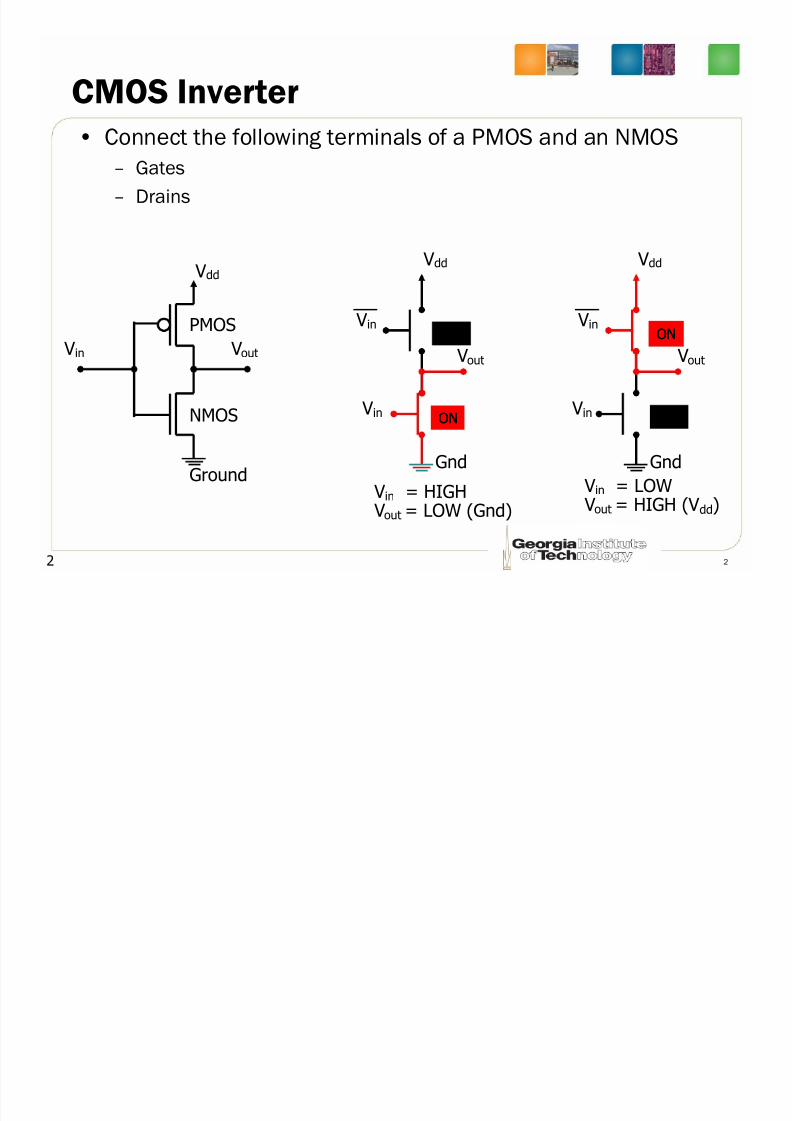
CMOS Inverter• Connect the following terminals of a PMOS and an NMOS
– Gates
– Drains
Vdd Vdd Vdd
2 2
Vin Vout
Gnd
Vout
Vin
Vin
Vin = HIGH Vout = LOW (Gnd)
ONON
OFFOFF
Gnd
Vout
Vin
Vin
Vin = LOW Vout = HIGH (Vdd)
ONON
OFFOFF
PMOS
Ground
NMOS
8/3/2019 Circuitos CMOS
http://slidepdf.com/reader/full/circuitos-cmos 3/34
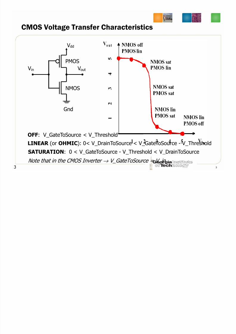
CMOS Voltage Transfer Characteristics
Vdd
Vin VoutPMOS
NMOS
3 3
Gnd
OFF: V_GateToSource < V_Threshold
LINEAR (or OHMIC): 0< V_DrainToSource < V_GateToSource - V_Threshold
SATURATION: 0 < V_GateToSource - V_Threshold < V_DrainToSource
Note that in the CMOS Inverter → V_GateToSource = V_in
8/3/2019 Circuitos CMOS
http://slidepdf.com/reader/full/circuitos-cmos 4/34
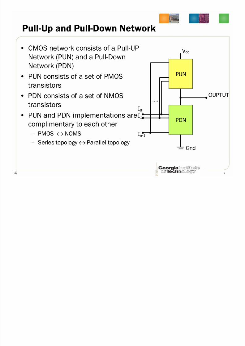
Pull-Up and Pull-Down Network• CMOS network consists of a Pull-UP
Network (PUN) and a Pull-Down
Network (PDN)• PUN consists of a set of PMOS
transistors
Vdd
PUN
4 4
• cons s s o a se otransistors
• PUN and PDN implementations arecomplimentary to each other
– PMOS ↔ NOMS– Series topology ↔ Parallel topology
….I0
I1
In-1
Gnd
PDN
8/3/2019 Circuitos CMOS
http://slidepdf.com/reader/full/circuitos-cmos 5/34
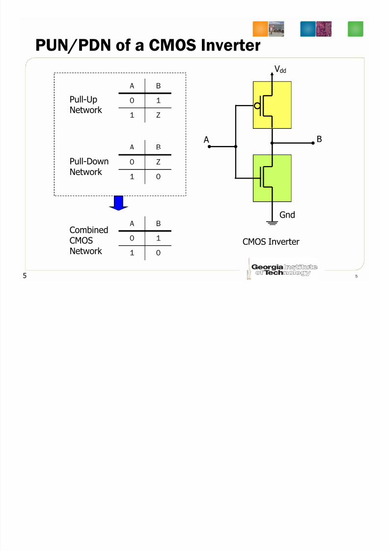
PUN/PDN of a CMOS Inverter
A B
0 1
1 Z
A B
Pull-UpNetwork
Vdd
A B
5 5
0 Z
1 0
A B
0 1
1 0
Pull-DownNetwork
CombinedCMOSNetwork
Gnd
CMOS Inverter
8/3/2019 Circuitos CMOS
http://slidepdf.com/reader/full/circuitos-cmos 6/34
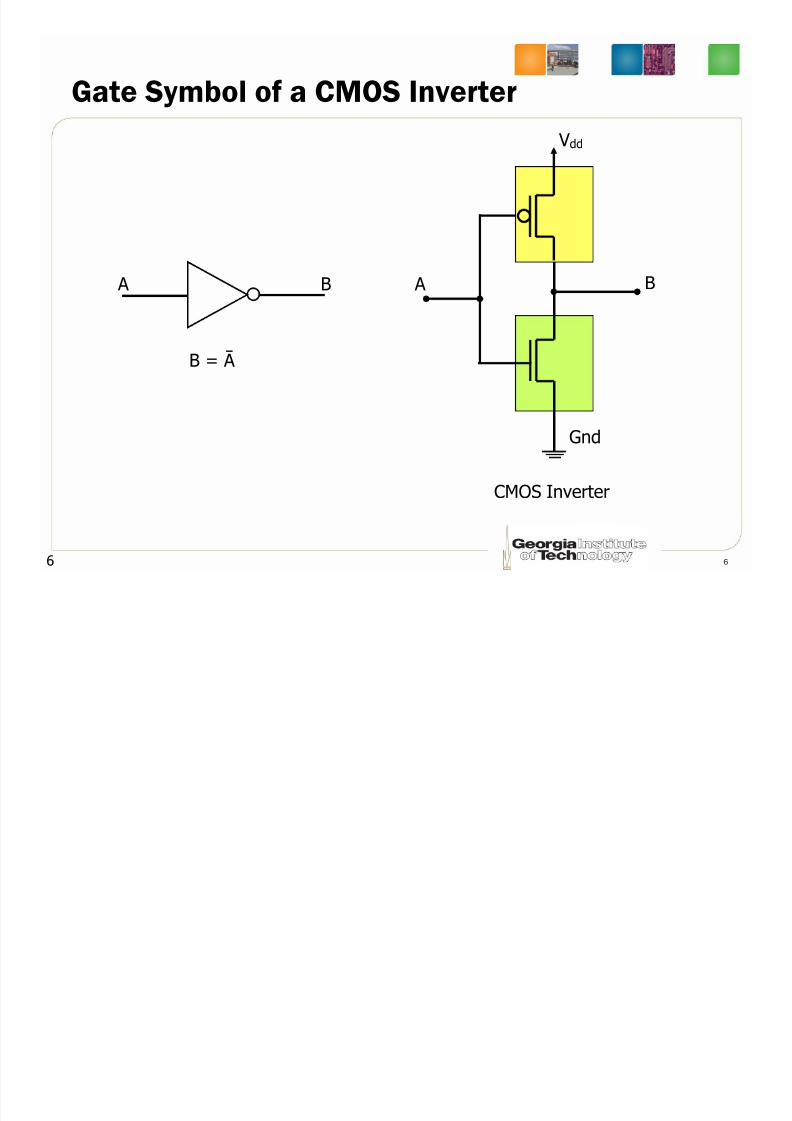
Gate Symbol of a CMOS Inverter
Vdd
A B A B
6 6
Gnd
CMOS Inverter
B = Ā
8/3/2019 Circuitos CMOS
http://slidepdf.com/reader/full/circuitos-cmos 7/34
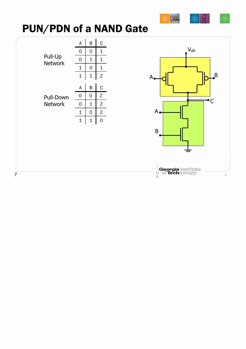
PUN/PDN of a NAND GateA B C
0 0 1
0 1 1
1 0 1
1 1 Z
A B C
Pull-UpNetwork
Vdd
A B
7 7
0 1 Z
1 0 Z
1 1 0
Pull-DownNetwork A
B
C
8/3/2019 Circuitos CMOS
http://slidepdf.com/reader/full/circuitos-cmos 8/34
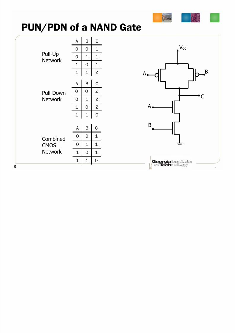
PUN/PDN of a NAND GateA B C
0 0 1
0 1 1
1 0 1
1 1 Z
A B C
Pull-UpNetwork
Vdd
A B
8 8
0 1 Z
1 0 Z
1 1 0
A B C
0 0 1
0 1 1
1 0 1
1 1 0
Pull-DownNetwork
CombinedCMOSNetwork
A
B
C
8/3/2019 Circuitos CMOS
http://slidepdf.com/reader/full/circuitos-cmos 9/34
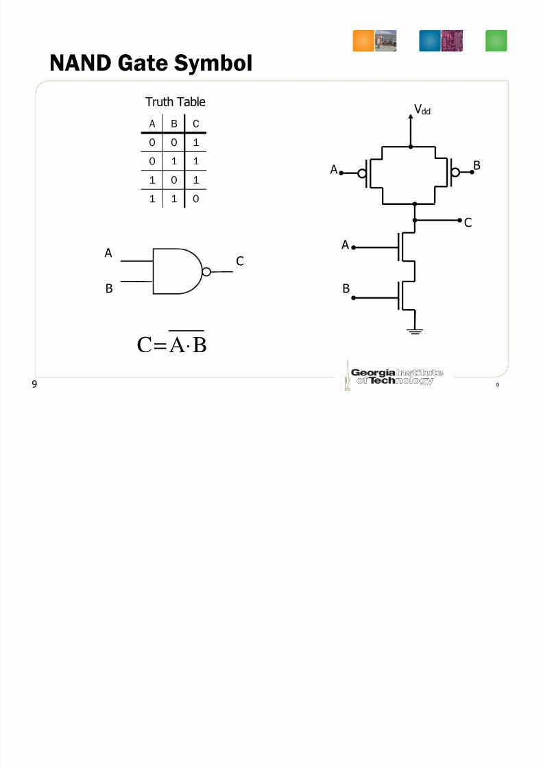
NAND Gate Symbol
A B C
0 0 10 1 1
1 0 1
1 1 0
Vdd
A B
Truth Table
9 9
A
B
C
A
B
C
BAC ⋅=
8/3/2019 Circuitos CMOS
http://slidepdf.com/reader/full/circuitos-cmos 10/34
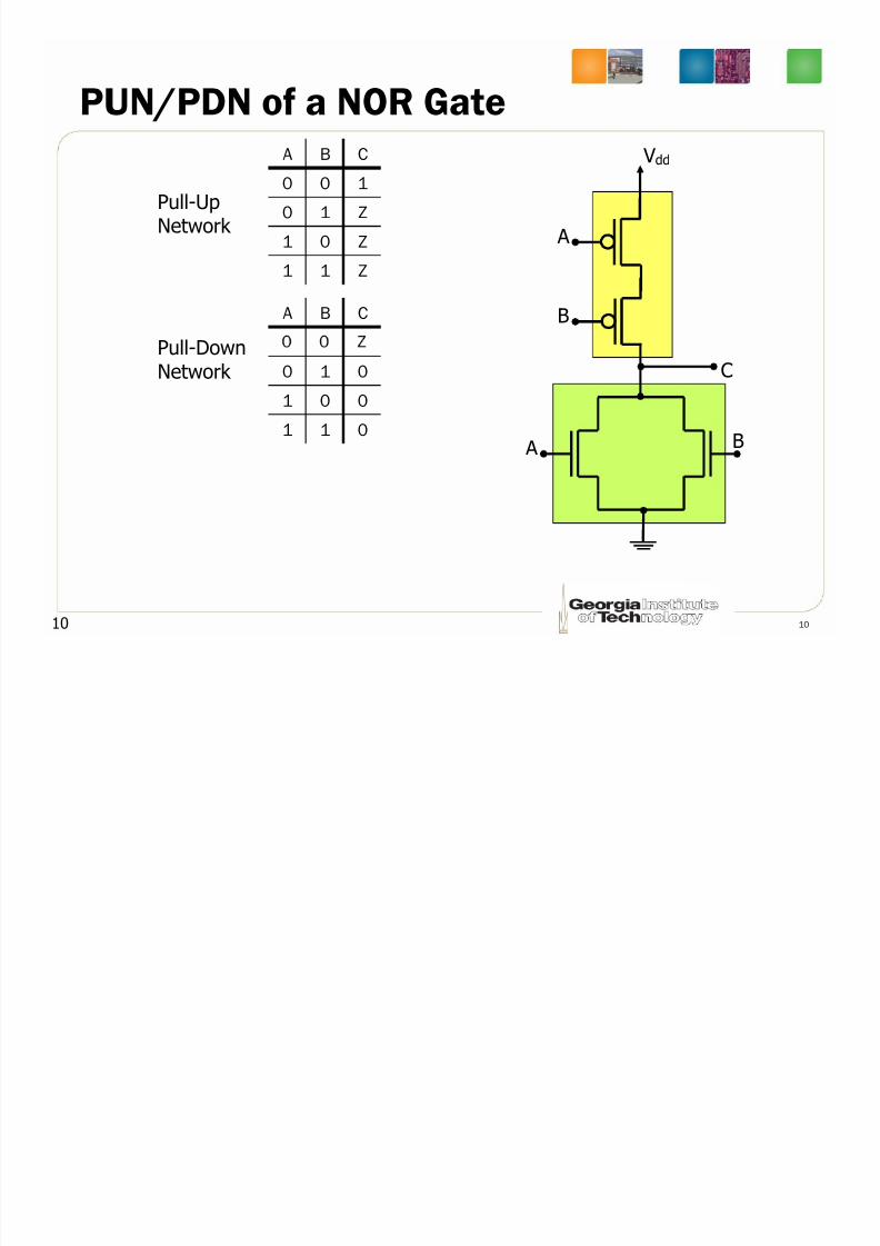
PUN/PDN of a NOR GateA B C
0 0 1
0 1 Z
1 0 Z
1 1 Z
A B C
Pull-UpNetwork
Vdd
A
B
10 10
0 1 0
1 0 0
1 1 0
Pull-DownNetwork C
A B
8/3/2019 Circuitos CMOS
http://slidepdf.com/reader/full/circuitos-cmos 11/34
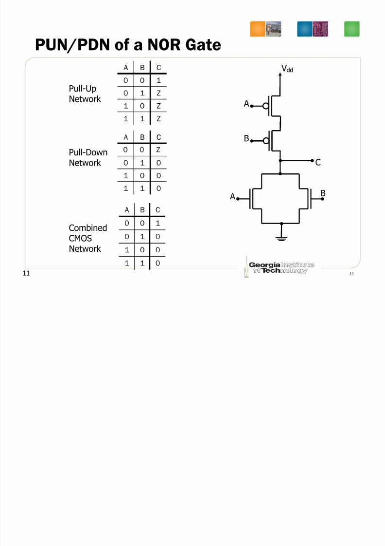
PUN/PDN of a NOR GateA B C
0 0 1
0 1 Z
1 0 Z
1 1 Z
A B C
Pull-UpNetwork
A
B
Vdd
11 11
0 1 0
1 0 0
1 1 0
A B C
0 0 1
0 1 0
1 0 0
1 1 0
Pull-DownNetwork
CombinedCMOSNetwork
C
A B
8/3/2019 Circuitos CMOS
http://slidepdf.com/reader/full/circuitos-cmos 12/34
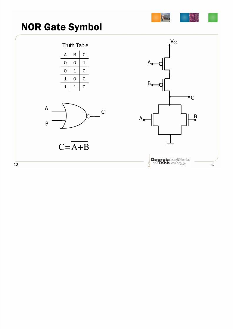
NOR Gate Symbol
A B C
0 0 10 1 0
1 0 0
1 1 0
Truth Table
A
B
Vdd
12 12
A
B
C
C
A B
BAC +=
8/3/2019 Circuitos CMOS
http://slidepdf.com/reader/full/circuitos-cmos 13/34
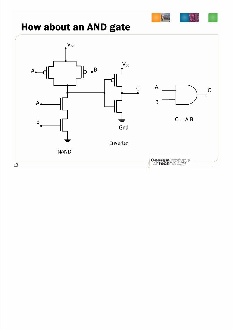
How about an AND gate
Vdd
A Vdd
B
A
13 13
A
B
Gnd
NAND
Inverter
C = A B
B
8/3/2019 Circuitos CMOS
http://slidepdf.com/reader/full/circuitos-cmos 14/34
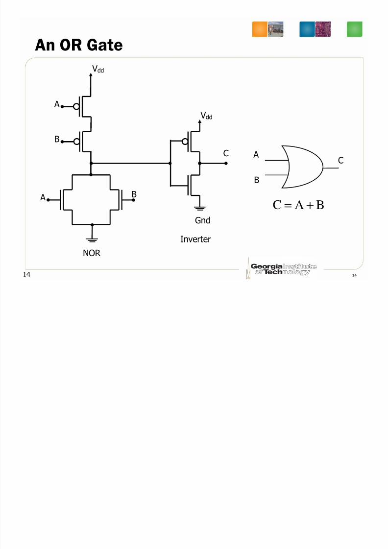
An OR Gate
A
B
Vdd
Vdd
14 14
A B
Gnd
C
Inverter
NOR
A
B
C
BAC+=
8/3/2019 Circuitos CMOS
http://slidepdf.com/reader/full/circuitos-cmos 15/34
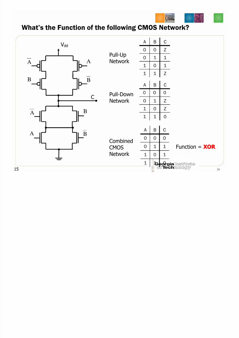
What’s the Function of the following CMOS Network?
A B C
0 0 Z
0 1 1
1 0 11 1 Z
A B C
Pull-UpNetwork
Vdd
A
B
A
B
15 15
0 1 Z
1 0 Z
1 1 0
A B C
0 0 0
0 1 1
1 0 1
1 1 0
Pull-DownNetwork
CombinedCMOSNetwork
Function = XOR XOR
A
A
B
B
C
8/3/2019 Circuitos CMOS
http://slidepdf.com/reader/full/circuitos-cmos 16/34
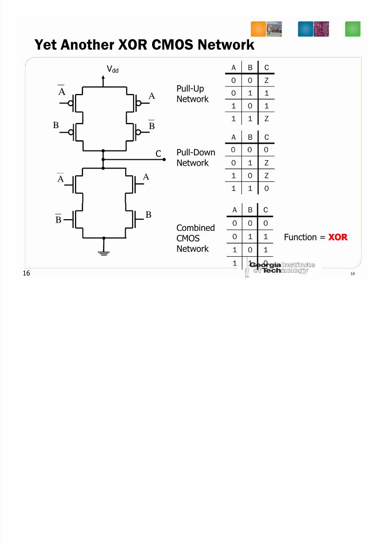
Yet Another XOR CMOS Network
Vdd
A
B
A
B
A B C
0 0 Z
0 1 1
1 0 11 1 Z
A B C
Pull-UpNetwork
16 16
A A
BB
C 0 1 Z
1 0 Z
1 1 0
A B C0 0 0
0 1 1
1 0 1
1 1 0
Pull-DownNetwork
CombinedCMOSNetwork
Function = XOR XOR
8/3/2019 Circuitos CMOS
http://slidepdf.com/reader/full/circuitos-cmos 17/34
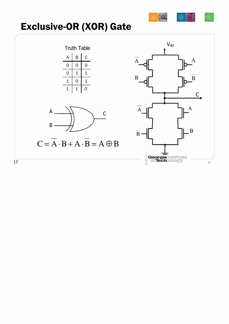
Exclusive-OR (XOR) Gate
Vdd
A
B
A
B
A B C
0 0 0
0 1 1
1 0 1
Truth Table
17 17
A A
BB
C
A
B
C
BABABAC ⊕=⋅+⋅=
8/3/2019 Circuitos CMOS
http://slidepdf.com/reader/full/circuitos-cmos 18/34
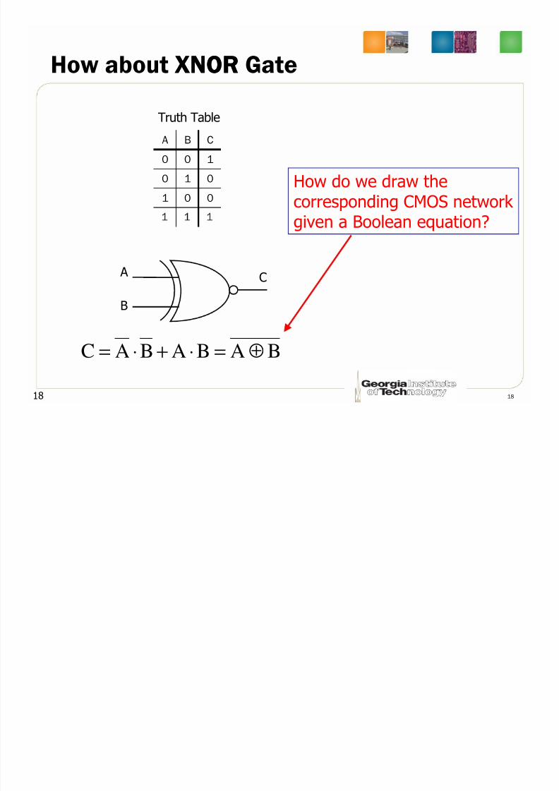
How about XNORXNOR Gate
A B C
0 0 1
0 1 0
1 0 0
Truth Table
How do we draw thecorresponding CMOS network
18 18
A
B
C
BABABAC ⊕=⋅+⋅=
given a Boolean equation?
8/3/2019 Circuitos CMOS
http://slidepdf.com/reader/full/circuitos-cmos 19/34
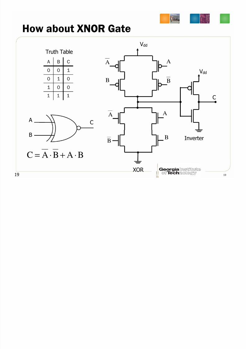
How about XNORXNOR Gate
A B C
0 0 1
0 1 0
1 0 0
Truth Table Vdd
A
B
A
B
Vdd
19 19
A
B
C
BABAC ⋅+⋅=
A A
BB
C
XOR
Inverter
8/3/2019 Circuitos CMOS
http://slidepdf.com/reader/full/circuitos-cmos 20/34
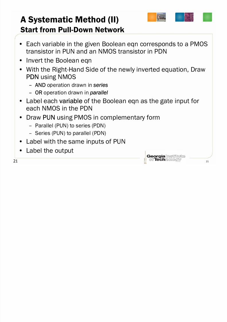
A Systematic Method (I)
Start from Pull-Up Network• Each variable in the given Boolean eqn corresponds to
a PMOS transistor in PUN and an NMOS transistor in
PDN• Draw PUNPUN using PMOS based on the Boolean eqn–– ANDAND operation drawn in series series
––
20 20
• Invert each variablevariable of the Boolean eqn as the gateinput for each PMOS in the PUN
• Draw PDNPDN using NMOS in complementary form
– Parallel (PUN) to series (PDN)– Series (PUN) to parallel (PDN)
• Label with the same inputs of PUN• Label the output
8/3/2019 Circuitos CMOS
http://slidepdf.com/reader/full/circuitos-cmos 21/34
A Systematic Method (II)
Start from Pull-Down Network• Each variable in the given Boolean eqn corresponds to a PMOS
transistor in PUN and an NMOS transistor in PDN
• Invert the Boolean eqn• With the Right-Hand Side of the newly inverted equation, DrawPDNPDN using NMOS–– ANDAND o eration drawn in series series
21 21
–– OROR operation drawn in parallelparallel• Label each variablevariable of the Boolean eqn as the gate input for
each NMOS in the PDN
• Draw PUNPUN using PMOS in complementary form
– Parallel (PUN) to series (PDN)– Series (PUN) to parallel (PDN)
• Label with the same inputs of PUN
• Label the output
8/3/2019 Circuitos CMOS
http://slidepdf.com/reader/full/circuitos-cmos 22/34
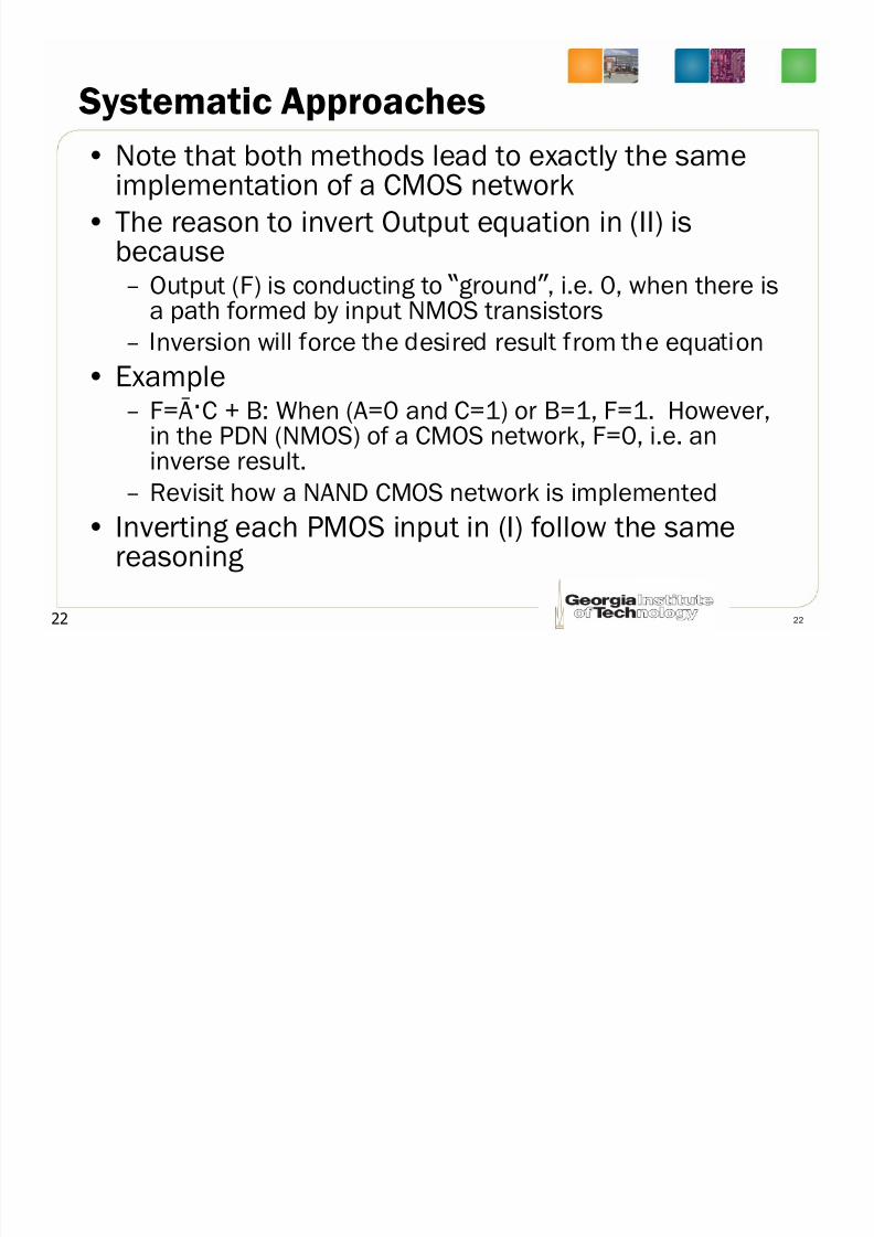
Systematic Approaches
• Note that both methods lead to exactly the sameimplementation of a CMOS network
• The reason to invert Output equation in (II) isbecause– Output (F) is conducting to “ground” , i.e. 0, when there is
a path formed by input NMOS transistors
22 22
– nvers on w orce e es re resu rom e equa on
• Example– F=Ā·C + B: When (A=0 and C=1) or B=1, F=1. However,
in the PDN (NMOS) of a CMOS network, F=0, i.e. aninverse result.
– Revisit how a NAND CMOS network is implemented
• Inverting each PMOS input in (I) follow the samereasoning
8/3/2019 Circuitos CMOS
http://slidepdf.com/reader/full/circuitos-cmos 23/34
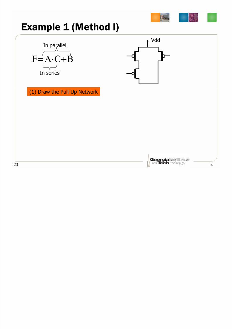
Example 1 (Method I)
BCAF +⋅=
In series
In parallel Vdd
23 23
(1) Draw the Pull-Up Network
8/3/2019 Circuitos CMOS
http://slidepdf.com/reader/full/circuitos-cmos 24/34
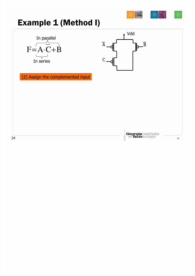
Example 1 (Method I)
BCAF +⋅=
In series
In parallel Vdd
A
C
B
24 24
(2) Assign the complemented input
8/3/2019 Circuitos CMOS
http://slidepdf.com/reader/full/circuitos-cmos 25/34
8/3/2019 Circuitos CMOS
http://slidepdf.com/reader/full/circuitos-cmos 26/34
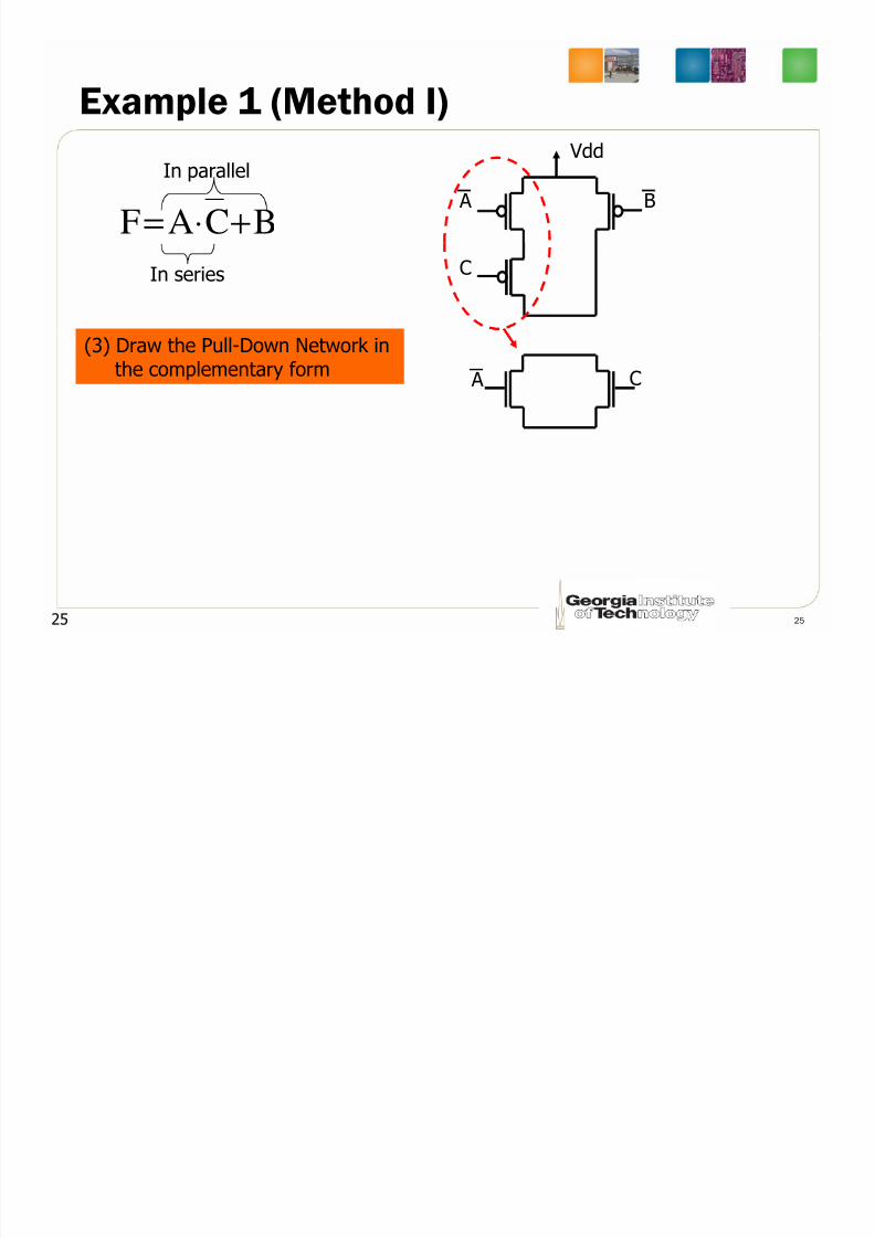
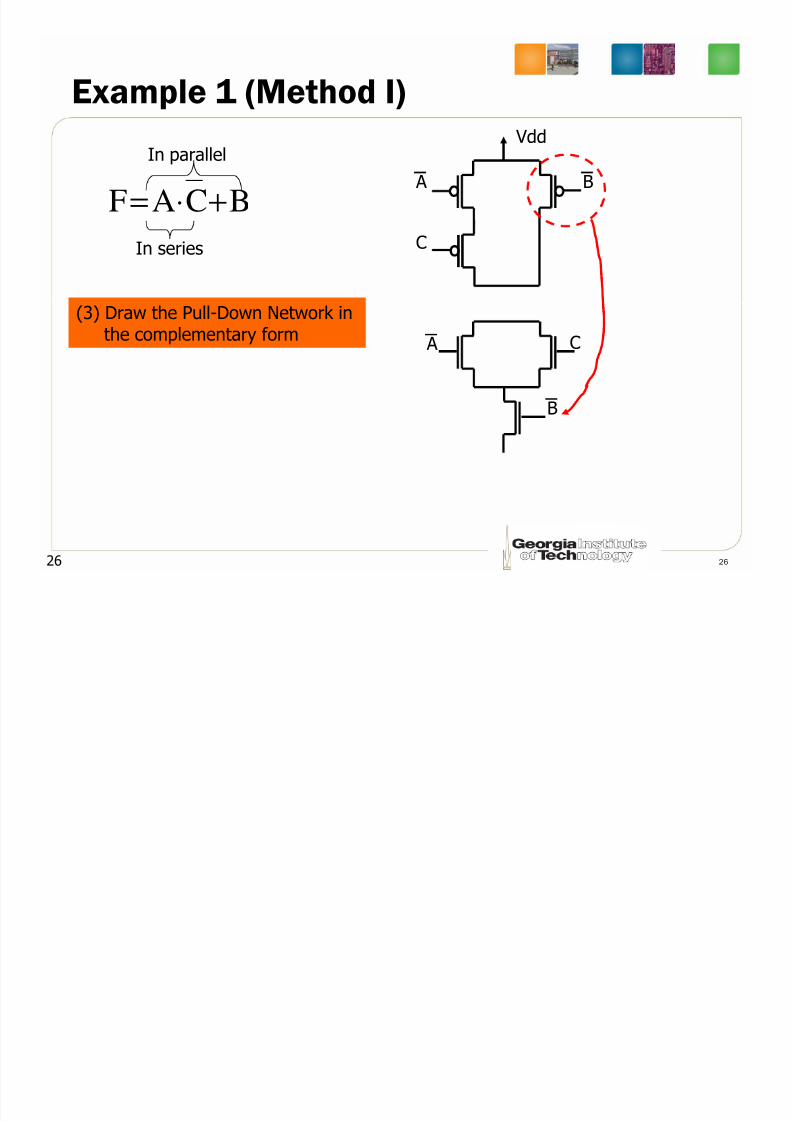
Example 1 (Method I)
BCAF +⋅=
In series
In parallel Vdd
A
C
B
26 26
(3) Draw the Pull-Down Network inthe complementary form A C
B
8/3/2019 Circuitos CMOS
http://slidepdf.com/reader/full/circuitos-cmos 27/34
Example 1 (Method I)
BCAF +⋅=
In series
In parallel Vdd
A
C
B
F
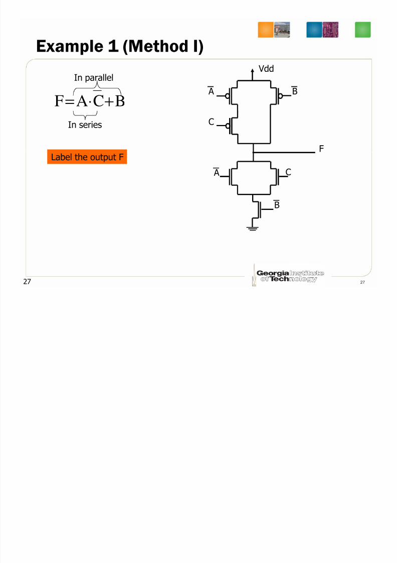
27 27
Label the output F
A C
B
8/3/2019 Circuitos CMOS
http://slidepdf.com/reader/full/circuitos-cmos 28/34
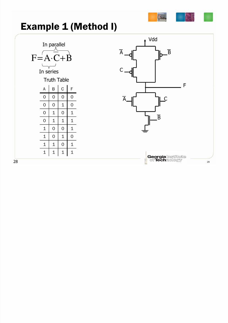
Example 1 (Method I)
BCAF +⋅=
In series
In parallel Vdd
A
C
B
FTruth Table
28 28
A C
B
0 0 0 0
0 0 1 0
0 1 0 1
0 1 1 1
1 0 0 1
1 0 1 0
1 1 0 1
1 1 1 1
8/3/2019 Circuitos CMOS
http://slidepdf.com/reader/full/circuitos-cmos 29/34
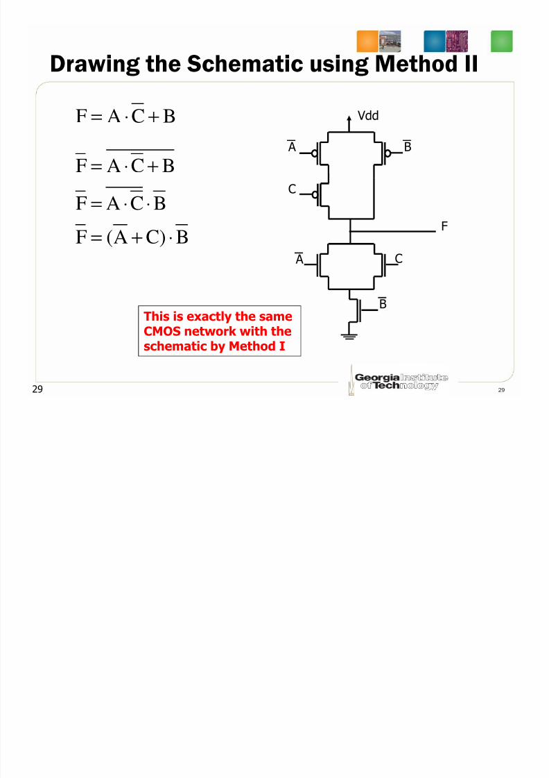
Drawing the Schematic using Method II
BCAF +⋅=
BCAF
BCAF
⋅⋅=
+⋅=
Vdd
A
C
B
29 29
BC)A(F
⋅+=
A C
B
F
This is exactly the sameCMOS network with theschematic by Method I
8/3/2019 Circuitos CMOS
http://slidepdf.com/reader/full/circuitos-cmos 30/34
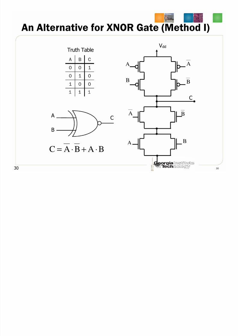
An Alternative for XNOR Gate (Method I)
A B C
0 0 1
0 1 0
1 0 0
Truth Table Vdd
A
B
A
B
30 30
A
B
C
BABAC ⋅+⋅=
A
A B
B
C
8/3/2019 Circuitos CMOS
http://slidepdf.com/reader/full/circuitos-cmos 31/34
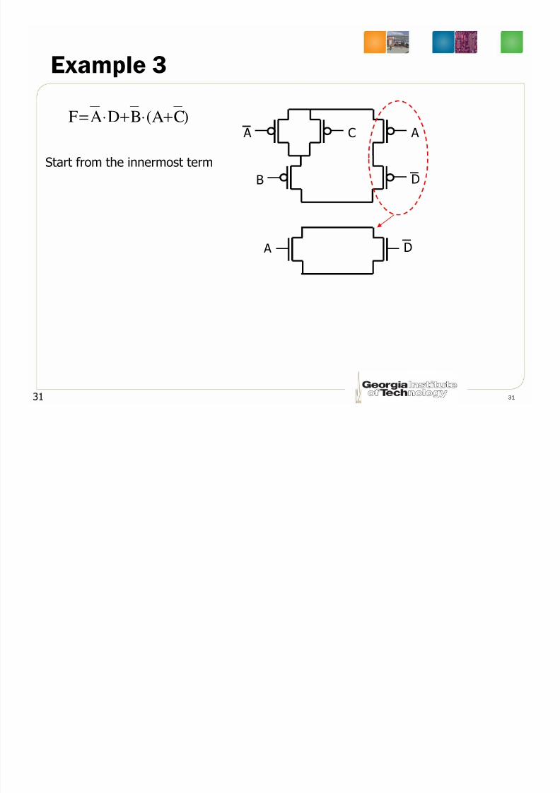
Example 3
)C(ABDAF +⋅+⋅=
Start from the innermost term
A
B D
A C
31 31
A D
8/3/2019 Circuitos CMOS
http://slidepdf.com/reader/full/circuitos-cmos 32/34
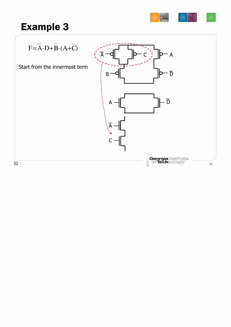
Example 3
)C(ABDAF +⋅+⋅=
Start from the innermost term
A
B D
A C
32 32
A D
A
C
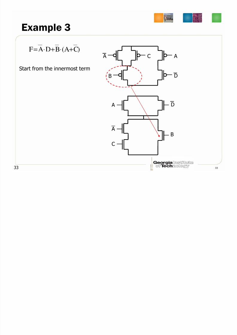
8/3/2019 Circuitos CMOS
http://slidepdf.com/reader/full/circuitos-cmos 33/34
Example 3
)C(ABDAF +⋅+⋅=
Start from the innermost term
A
B D
A C
33 33
A D
A
C
B
8/3/2019 Circuitos CMOS
http://slidepdf.com/reader/full/circuitos-cmos 34/34
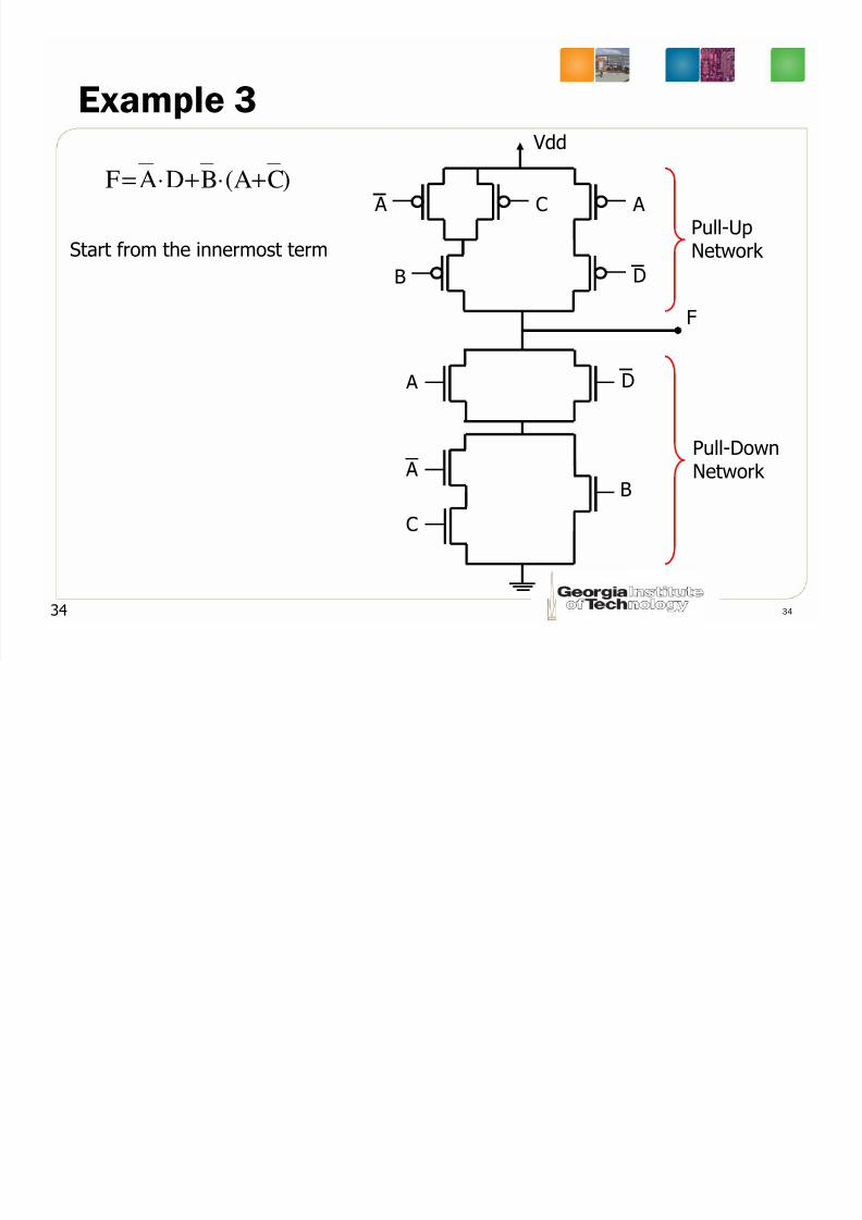
Example 3
)C(ABDAF +⋅+⋅=
Start from the innermost term
A
B D
A C
Vdd
F
Pull-UpNetwork
34 34
A D
A
C
B
Pull-Down
Network