ads1294 24 bits
DESCRIPTION
TRANSCRIPT
Control
CL
KG
PIO
AN
D C
ON
TR
OL
Oscillator
SPI
Test Signals and
Monitors
PACE
SP
I
RLD
Wilson
TerminalWCT
Reference
REF
ADC7
ADC8
ADC1
ADC2
ADC3
ADC4
ADC5
ADC6
A7
A8
A1
A2
A3
A4
A5
A6
MUX
INP
UT
S
¼ ¼
¼
To Channel
RESP
Resp
RESP
DEMOD
ADS129xR
ADS129xR
ADS1294, ADS1294RADS1296, ADS1296RADS1298, ADS1298R
www.ti.com SBAS459I –JANUARY 2010–REVISED JANUARY 2012
Low-Power, 8-Channel, 24-Bit Analog Front-End for Biopotential MeasurementsCheck for Samples: ADS1294, ADS1294R, ADS1296, ADS1296R, ADS1298, ADS1298R
With its high levels of integration and exceptional1FEATURES
performance, the ADS1294/6/8/4R/6R/8R family23• Eight Low-Noise PGAs and Eight enables the development of scalable medical
High-Resolution ADCs (ADS1298, ADS1298R) instrumentation systems at significantly reduced size,• Low Power: 0.75mW/channel power, and overall cost.• Input-Referred Noise: 4μVPP (150Hz BW, G = 6) The ADS1294/6/8/4R/6R/8R have a flexible input
multiplexer per channel that can be independently• Input Bias Current: 200pAconnected to the internally-generated signals for test,• Data Rate: 250SPS to 32kSPStemperature, and lead-off detection. Additionally, any
• CMRR: –115dB configuration of input channels can be selected for• Programmable Gain: 1, 2, 3, 4, 6, 8, or 12 derivation of the right leg drive (RLD) output signal.
The ADS1294/6/8/4R/6R/8R operate at data rates as• Supports AAMI EC11, EC13, IEC60601-1,high as 32kSPS, thereby allowing the implementationIEC60601-2-27, and IEC60601-2-51 Standardsof software PACE detection. Lead-off detection can
• Unipolar or Bipolar Supplies: be implemented internal to the device, either with aAVDD = 2.7V to 5.25V, DVDD = 1.65V to 3.6V pull-up/pull-down resistor or an excitation current
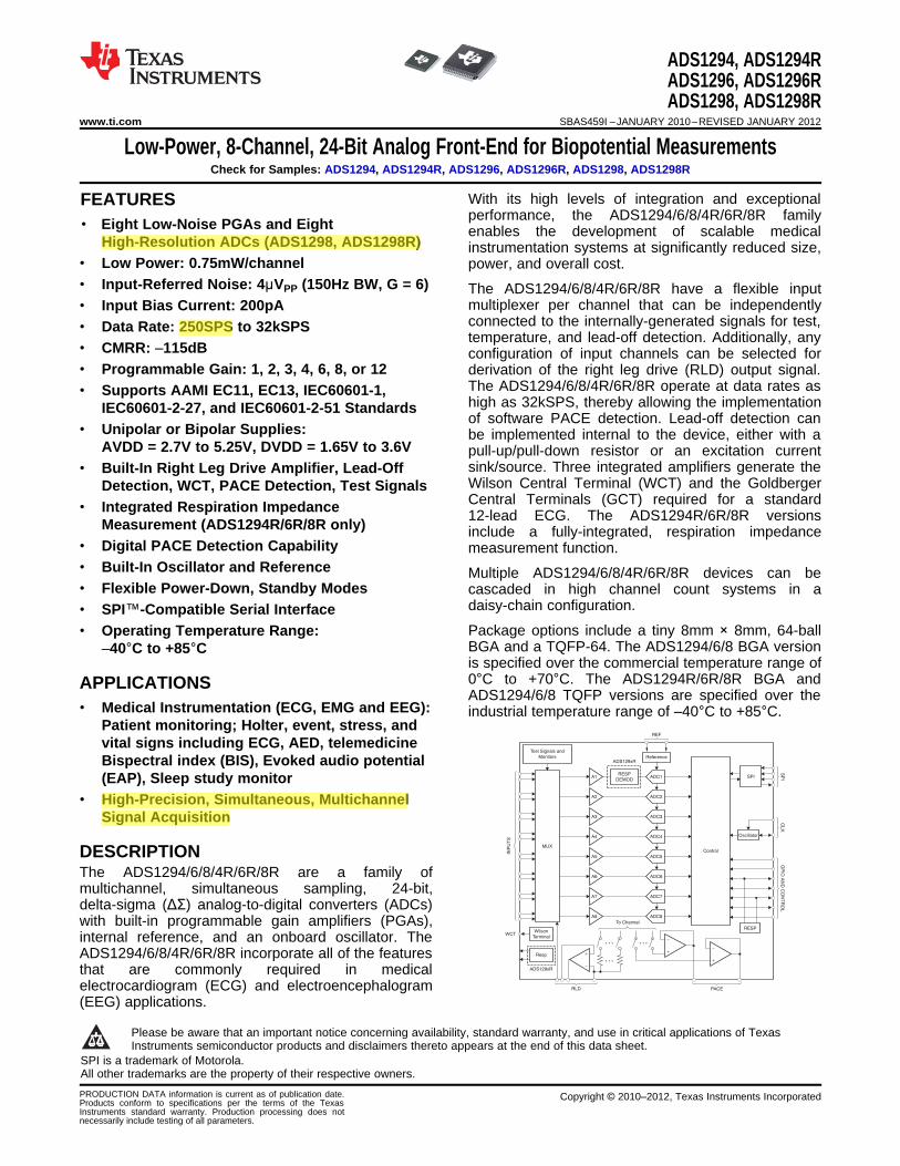
sink/source. Three integrated amplifiers generate the• Built-In Right Leg Drive Amplifier, Lead-OffWilson Central Terminal (WCT) and the GoldbergerDetection, WCT, PACE Detection, Test SignalsCentral Terminals (GCT) required for a standard• Integrated Respiration Impedance12-lead ECG. The ADS1294R/6R/8R versions
Measurement (ADS1294R/6R/8R only) include a fully-integrated, respiration impedance• Digital PACE Detection Capability measurement function.• Built-In Oscillator and Reference Multiple ADS1294/6/8/4R/6R/8R devices can be• Flexible Power-Down, Standby Modes cascaded in high channel count systems in a
daisy-chain configuration.• SPI™-Compatible Serial InterfacePackage options include a tiny 8mm × 8mm, 64-ball• Operating Temperature Range:BGA and a TQFP-64. The ADS1294/6/8 BGA version–40°C to +85°Cis specified over the commercial temperature range of0°C to +70°C. The ADS1294R/6R/8R BGA andAPPLICATIONSADS1294/6/8 TQFP versions are specified over the
• Medical Instrumentation (ECG, EMG and EEG): industrial temperature range of –40°C to +85°C.Patient monitoring; Holter, event, stress, andvital signs including ECG, AED, telemedicineBispectral index (BIS), Evoked audio potential(EAP), Sleep study monitor
• High-Precision, Simultaneous, MultichannelSignal Acquisition
DESCRIPTIONThe ADS1294/6/8/4R/6R/8R are a family ofmultichannel, simultaneous sampling, 24-bit,delta-sigma (ΔΣ) analog-to-digital converters (ADCs)with built-in programmable gain amplifiers (PGAs),internal reference, and an onboard oscillator. TheADS1294/6/8/4R/6R/8R incorporate all of the featuresthat are commonly required in medicalelectrocardiogram (ECG) and electroencephalogram(EEG) applications.1
Please be aware that an important notice concerning availability, standard warranty, and use in critical applications of TexasInstruments semiconductor products and disclaimers thereto appears at the end of this data sheet.
2SPI is a trademark of Motorola.3All other trademarks are the property of their respective owners.
PRODUCTION DATA information is current as of publication date. Copyright © 2010–2012, Texas Instruments IncorporatedProducts conform to specifications per the terms of the TexasInstruments standard warranty. Production processing does notnecessarily include testing of all parameters.
ADS1294, ADS1294RADS1296, ADS1296RADS1298, ADS1298RSBAS459I –JANUARY 2010–REVISED JANUARY 2012 www.ti.com
This integrated circuit can be damaged by ESD. Texas Instruments recommends that all integrated circuits be handled withappropriate precautions. Failure to observe proper handling and installation procedures can cause damage.
ESD damage can range from subtle performance degradation to complete device failure. Precision integrated circuits may be moresusceptible to damage because very small parametric changes could cause the device not to meet its published specifications.
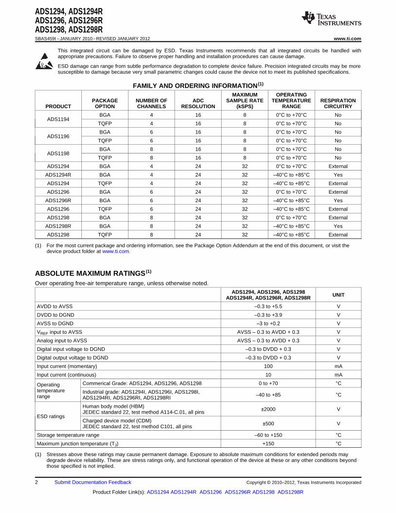
FAMILY AND ORDERING INFORMATION (1)
MAXIMUM OPERATINGPACKAGE NUMBER OF ADC SAMPLE RATE TEMPERATURE RESPIRATION
PRODUCT OPTION CHANNELS RESOLUTION (kSPS) RANGE CIRCUITRY
BGA 4 16 8 0°C to +70°C NoADS1194
TQFP 4 16 8 0°C to +70°C No
BGA 6 16 8 0°C to +70°C NoADS1196
TQFP 6 16 8 0°C to +70°C No
BGA 8 16 8 0°C to +70°C NoADS1198
TQFP 8 16 8 0°C to +70°C No
ADS1294 BGA 4 24 32 0°C to +70°C External
ADS1294R BGA 4 24 32 –40°C to +85°C Yes
ADS1294 TQFP 4 24 32 –40°C to +85°C External
ADS1296 BGA 6 24 32 0°C to +70°C External
ADS1296R BGA 6 24 32 –40°C to +85°C Yes
ADS1296 TQFP 6 24 32 –40°C to +85°C External
ADS1298 BGA 8 24 32 0°C to +70°C External
ADS1298R BGA 8 24 32 –40°C to +85°C Yes
ADS1298 TQFP 8 24 32 –40°C to +85°C External
(1) For the most current package and ordering information, see the Package Option Addendum at the end of this document, or visit thedevice product folder at www.ti.com.
ABSOLUTE MAXIMUM RATINGS (1)
Over operating free-air temperature range, unless otherwise noted.
ADS1294, ADS1296, ADS1298 UNITADS1294R, ADS1296R, ADS1298R
AVDD to AVSS –0.3 to +5.5 V
DVDD to DGND –0.3 to +3.9 V
AVSS to DGND –3 to +0.2 V
VREF input to AVSS AVSS – 0.3 to AVDD + 0.3 V
Analog input to AVSS AVSS – 0.3 to AVDD + 0.3 V
Digital input voltage to DGND –0.3 to DVDD + 0.3 V
Digital output voltage to DGND –0.3 to DVDD + 0.3 V
Input current (momentary) 100 mA
Input current (continuous) 10 mA
Commerical Grade: ADS1294, ADS1296, ADS1298 0 to +70 °COperatingtemperature Industrial grade: ADS1294I, ADS1296I, ADS1298I, –40 to +85 °Crange ADS1294RI, ADS1296RI, ADS1298RI
Human body model (HBM) ±2000 VJEDEC standard 22, test method A114-C.01, all pinsESD ratings
Charged device model (CDM) ±500 VJEDEC standard 22, test method C101, all pins
Storage temperature range –60 to +150 °CMaximum junction temperature (TJ) +150 °C
(1) Stresses above these ratings may cause permanent damage. Exposure to absolute maximum conditions for extended periods maydegrade device reliability. These are stress ratings only, and functional operation of the device at these or any other conditions beyondthose specified is not implied.
2 Submit Documentation Feedback Copyright © 2010–2012, Texas Instruments Incorporated
Product Folder Link(s): ADS1294 ADS1294R ADS1296 ADS1296R ADS1298 ADS1298R

ADS1294, ADS1294RADS1296, ADS1296RADS1298, ADS1298R
www.ti.com SBAS459I –JANUARY 2010–REVISED JANUARY 2012
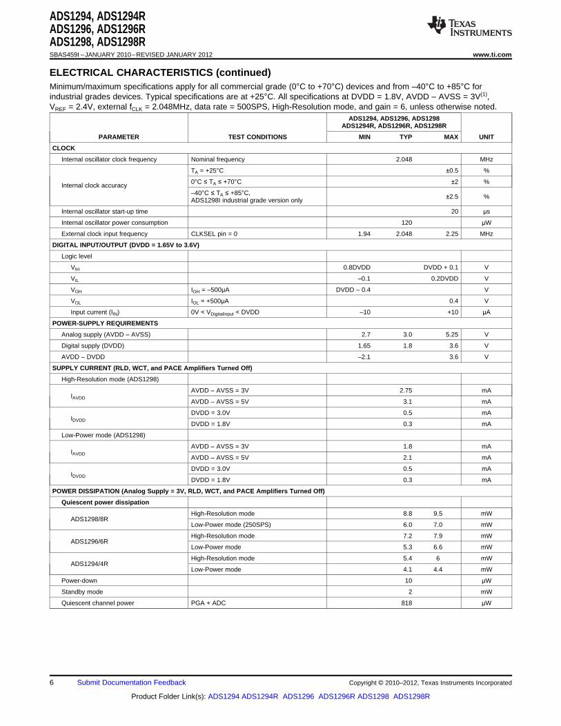
ELECTRICAL CHARACTERISTICSMinimum/maximum specifications apply for all commercial grade (0°C to +70°C) devices and from –40°C to +85°C forindustrial grades devices. Typical specifications are at +25°C. All specifications at DVDD = 1.8V, AVDD – AVSS = 3V (1),VREF = 2.4V, external fCLK = 2.048MHz, data rate = 500SPS, High-Resolution mode, and gain = 6, unless otherwise noted.
ADS1294, ADS1296, ADS1298ADS1294R, ADS1296R, ADS1298R
PARAMETER TEST CONDITIONS MIN TYP MAX UNIT
ANALOG INPUTS
Full-scale differential input voltage (AINP – AINN) ±VREF/GAIN V
See the Input Common-Mode RangeInput common-mode range subsection of the PGA Settings and Input
Range section
Input capacitance 20 pF
TA = +25°C, input = 1.5V ±200 pA
Input bias current TA = 0°C to +70°C, input = 1.5V ±1 nA
TA = –40°C to +85°C, input = 1.5V ±1.2 nA
No lead-off 1000 MΩ
DC input impedance Current source lead-off detection 500 MΩ
Pull-up resistor lead-off detection 10 MΩ
PGA PERFORMANCE
Gain settings 1, 2, 3, 4, 6, 8, 12
Bandwidth See Table 6
ADC PERFORMANCE
Data rates up to 8kSPS, no missing codes 24 Bits
Resolution 16kSPS data rate 19 Bits
32kSPS data rate 17 Bits
fCLK = 2.048MHz, High-Resolution mode 500 32000 SPSData rate
fCLK = 2.048MHz, Low-Power mode 250 16000 SPS
CHANNEL PERFORMANCE
DC Performance
Gain = 6 (2), 10 seconds of data 5 μVPP
Gain = 6, 256 points, 0.5 seconds of data 4 7 μVPPInput-referred noiseGain settings other than 6, data rates other See Noise Measurements sectionthan 500SPS
Full-scale with gain = 6, best fit 8 ppm
Full-scale with gain = 6, best fit, 40 ppmIntegral nonlinearity ADS1294R/6R/8R channel 1
–20dBFS with gain = 6, best fit, 8 ppmADS1294R/6R/8R channel 1
Offset error ±500 µV
Offset error drift 2 µV/°C
Gain error Excluding voltage reference error ±0.2 ±0.5 % of FS
Gain drift Excluding voltage reference drift 5 ppm/°C
Gain match between channels 0.3 % of FS
(1) Performance is applicable for 5V operation as well. Production testing for limits is performed at 3V.(2) Noise data measured in a 10-second interval. Test not performed in production. Input-referred noise is calculated with input shorted
(without electrode resistance) over a 10-second interval.
Copyright © 2010–2012, Texas Instruments Incorporated Submit Documentation Feedback 3
Product Folder Link(s): ADS1294 ADS1294R ADS1296 ADS1296R ADS1298 ADS1298R
ADS1294, ADS1294RADS1296, ADS1296RADS1298, ADS1298RSBAS459I –JANUARY 2010–REVISED JANUARY 2012 www.ti.com
ELECTRICAL CHARACTERISTICS (continued)Minimum/maximum specifications apply for all commercial grade (0°C to +70°C) devices and from –40°C to +85°C forindustrial grades devices. Typical specifications are at +25°C. All specifications at DVDD = 1.8V, AVDD – AVSS = 3V(1),VREF = 2.4V, external fCLK = 2.048MHz, data rate = 500SPS, High-Resolution mode, and gain = 6, unless otherwise noted.
ADS1294, ADS1296, ADS1298ADS1294R, ADS1296R, ADS1298R
PARAMETER TEST CONDITIONS MIN TYP MAX UNIT
CHANNEL PERFORMANCE (continued)
AC Performance
Common-mode rejection ratio (CMRR) fCM = 50Hz, 60Hz (3) –105 –115 dB
Power-supply rejection ratio (PSRR) fPS = 50Hz, 60Hz 90 dB
Crosstalk fIN = 50Hz, 60Hz –126 dB
Signal-to-noise ratio (SNR) fIN = 10Hz input, gain = 6 112 dB
10Hz, –0.5dBFs –98 dB
ADS1294R/6R/8R channel 1, 10Hz, –0.5dBFs –70 dB
100Hz, –0.5dBFs (4) –100 dBTotal harmonic distortion (THD)
ADS1294R/6R/8R channel 1, –68 dB100Hz, –0.5dBFs (4)
ADS1294R/6R/8R channel 1, –86 dB100Hz, –20dBFs (4)
DIGITAL FILTER
–3dB bandwidth 0.262fDR Hz
Digital filter settling Full setting 4 Conversions
RIGHT LEG DRIVE (RLD) AMPLIFIER AND PACE AMPLIFIERS
RLD integrated noise BW = 150Hz 7 μVRMS
PACE integrated noise BW = 8kHz 20 µVRMS
PACE amplifier crosstalk Crosstalk between PACE amplifiers 60 dB
Gain bandwidth product 50kΩ || 10pF load, gain = 1 100 kHz
Slew rate 50kΩ || 10pF load, gain = 1 0.25 V/μs
Short-circuit to GND (AVDD = 3V) 270 μA
Short-circuit to supply (AVDD = 3V) 550 μAPACE and RLD amplifier drive strength
Short-circuit to GND (AVDD = 5V) 490 μA
Short-circuit to supply (AVDD = 5V) 810 μA
Peak swing (AVSS + 0.3V to AVDD + 0.3V) 50 μAat AVDD = 3VPACE and RLD current
Peak swing (AVSS + 0.3V to AVDD + 0.3V) 75 μAat AVDD = 5V
PACE amplifier output resistance 100 Ω
Total harmonic distortion fIN = 100Hz, gain = 1 –70 dB
Common-mode input range AVSS + 0.7 AVDD – 0.3 V
Common-mode resistor matching Internal 200kΩ resistor matching 0.1 %
Short-circuit current ±0.25 mA
Quiescent power consumption Either RLD or PACE amplifier 20 μA
WILSON CENTRAL TERMINAL (WCT) AMPLIFIER
Integrated noise BW = 150Hz See Table 5 nV/√Hz
Gain bandwidth product See Table 5 kHz
Slew rate See Table 5 V/s
Total harmonic distortion fIN = 100Hz 90 dB
Common-mode input range AVSS + 0.3 AVDD – 0.3 V
Short-circuit current Through internal 30kΩ resistor ±0.25 mA
Quiescent power consumption See Table 5 μA
(3) CMRR is measured with a common-mode signal of AVSS + 0.3V to AVDD – 0.3V. The values indicated are the maximum of the eightchannels.
(4) Harmonics above the second harmonic are attenuated by the digital filter.
4 Submit Documentation Feedback Copyright © 2010–2012, Texas Instruments Incorporated
Product Folder Link(s): ADS1294 ADS1294R ADS1296 ADS1296R ADS1298 ADS1298R
ADS1294, ADS1294RADS1296, ADS1296RADS1298, ADS1298R
www.ti.com SBAS459I –JANUARY 2010–REVISED JANUARY 2012
ELECTRICAL CHARACTERISTICS (continued)Minimum/maximum specifications apply for all commercial grade (0°C to +70°C) devices and from –40°C to +85°C forindustrial grades devices. Typical specifications are at +25°C. All specifications at DVDD = 1.8V, AVDD – AVSS = 3V(1),VREF = 2.4V, external fCLK = 2.048MHz, data rate = 500SPS, High-Resolution mode, and gain = 6, unless otherwise noted.
ADS1294, ADS1296, ADS1298ADS1294R, ADS1296R, ADS1298R
PARAMETER TEST CONDITIONS MIN TYP MAX UNIT
LEAD-OFF DETECT
Frequency See the Register Map section for settings 0, fDR/4 kHz
Current See the Register Map section for settings 6, 12, 18, 24 nA
Current accuracy ±20 %
Comparator threshold accuracy ±30 mV
RESPIRATION (ADS1294R/6R/8R Only)
Internal source 32, 64 kHzFrequency
External source 32 64 kHz
Phase shift See the Register Map section for settings 22.5 90 157.5 Degrees
Impedance range IRESP = 30μA 10 kΩ
0.05Hz to 2Hz brick wall filter, 32kHzmodulation clock, phase = 112.5,Impedance measurement noise 20 mΩPPusing IRESP = 30μA with 2kΩ baseline load,gain = 4 test condition
internal reference, signal path = 82kΩ,Modulator current 29 µAbaseline = 2.21kΩ
EXTERNAL REFERENCE
3V supply VREF = (VREFP – VREFN) 2.5 VReference input voltage
5V supply VREF = (VREFP – VREFN) 4.0 V
Negative input (VREFN) AVSS V
Positive input (VREFP) AVSS + 2.5 V
Input impedance 10 kΩ
INTERNAL REFERENCE
Register bit CONFIG3.VREF_4V = 0, 2.4 VAVDD ≥ 2.7VOutput voltage
Register bit CONFIG3.VREF_4V = 1, 4.0 VAVDD ≥ 4.4V
VREF accuracy ±0.2 %
TA = +25°C 35 ppm/°C
Internal reference drift Commerical grade, 0°C to +70°C 35 ppm
Industrial grade, –40°C to +85°C 45 ppm
Start-up time 150 ms
SYSTEM MONITORS
Analog supply reading error 2 %
Digital supply reading error 2 %
From power-up to DRDY low 150 msDevice wake up
STANDBY mode 9 ms
Temperature sensor reading, voltage TA = +25°C 145 mV
Temperature sensor reading, coefficient 490 μV/°C
Test Signal
Signal frequency See Register Map section for settings HzfCLK/221, fCLK/220
Signal voltage See Register Map section for settings ±1, ±2 mV
Accuracy ±2 %
Copyright © 2010–2012, Texas Instruments Incorporated Submit Documentation Feedback 5
Product Folder Link(s): ADS1294 ADS1294R ADS1296 ADS1296R ADS1298 ADS1298R
ADS1294, ADS1294RADS1296, ADS1296RADS1298, ADS1298RSBAS459I –JANUARY 2010–REVISED JANUARY 2012 www.ti.com
ELECTRICAL CHARACTERISTICS (continued)Minimum/maximum specifications apply for all commercial grade (0°C to +70°C) devices and from –40°C to +85°C forindustrial grades devices. Typical specifications are at +25°C. All specifications at DVDD = 1.8V, AVDD – AVSS = 3V(1),VREF = 2.4V, external fCLK = 2.048MHz, data rate = 500SPS, High-Resolution mode, and gain = 6, unless otherwise noted.
ADS1294, ADS1296, ADS1298ADS1294R, ADS1296R, ADS1298R
PARAMETER TEST CONDITIONS MIN TYP MAX UNIT
CLOCK
Internal oscillator clock frequency Nominal frequency 2.048 MHz
TA = +25°C ±0.5 %
0°C ≤ TA ≤ +70°C ±2 %Internal clock accuracy–40°C ≤ TA ≤ +85°C, ±2.5 %ADS1298I industrial grade version only
Internal oscillator start-up time 20 μs
Internal oscillator power consumption 120 μW
External clock input frequency CLKSEL pin = 0 1.94 2.048 2.25 MHz
DIGITAL INPUT/OUTPUT (DVDD = 1.65V to 3.6V)
Logic level
VIH 0.8DVDD DVDD + 0.1 V
VIL –0.1 0.2DVDD V
VOH IOH = –500μA DVDD – 0.4 V
VOL IOL = +500μA 0.4 V
Input current (IIN) 0V < VDigitalInput < DVDD –10 +10 μA
POWER-SUPPLY REQUIREMENTS
Analog supply (AVDD – AVSS) 2.7 3.0 5.25 V
Digital supply (DVDD) 1.65 1.8 3.6 V
AVDD – DVDD –2.1 3.6 V
SUPPLY CURRENT (RLD, WCT, and PACE Amplifiers Turned Off)
High-Resolution mode (ADS1298)
AVDD – AVSS = 3V 2.75 mAIAVDD
AVDD – AVSS = 5V 3.1 mA
DVDD = 3.0V 0.5 mAIDVDD
DVDD = 1.8V 0.3 mA
Low-Power mode (ADS1298)
AVDD – AVSS = 3V 1.8 mAIAVDD
AVDD – AVSS = 5V 2.1 mA
DVDD = 3.0V 0.5 mAIDVDD
DVDD = 1.8V 0.3 mA
POWER DISSIPATION (Analog Supply = 3V, RLD, WCT, and PACE Amplifiers Turned Off)
Quiescent power dissipation
High-Resolution mode 8.8 9.5 mWADS1298/8R
Low-Power mode (250SPS) 6.0 7.0 mW
High-Resolution mode 7.2 7.9 mWADS1296/6R
Low-Power mode 5.3 6.6 mW
High-Resolution mode 5.4 6 mWADS1294/4R
Low-Power mode 4.1 4.4 mW
Power-down 10 μW
Standby mode 2 mW
Quiescent channel power PGA + ADC 818 μW
6 Submit Documentation Feedback Copyright © 2010–2012, Texas Instruments Incorporated
Product Folder Link(s): ADS1294 ADS1294R ADS1296 ADS1296R ADS1298 ADS1298R
ADS1294, ADS1294RADS1296, ADS1296RADS1298, ADS1298R
www.ti.com SBAS459I –JANUARY 2010–REVISED JANUARY 2012
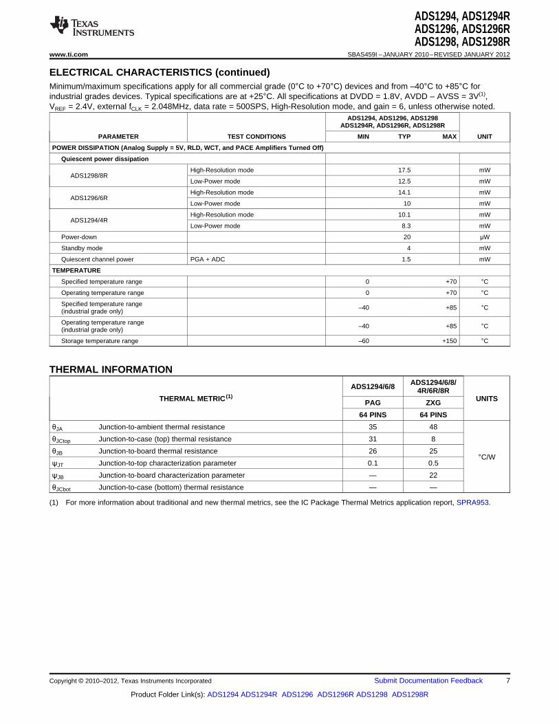
ELECTRICAL CHARACTERISTICS (continued)Minimum/maximum specifications apply for all commercial grade (0°C to +70°C) devices and from –40°C to +85°C forindustrial grades devices. Typical specifications are at +25°C. All specifications at DVDD = 1.8V, AVDD – AVSS = 3V(1),VREF = 2.4V, external fCLK = 2.048MHz, data rate = 500SPS, High-Resolution mode, and gain = 6, unless otherwise noted.
ADS1294, ADS1296, ADS1298ADS1294R, ADS1296R, ADS1298R
PARAMETER TEST CONDITIONS MIN TYP MAX UNIT
POWER DISSIPATION (Analog Supply = 5V, RLD, WCT, and PACE Amplifiers Turned Off)
Quiescent power dissipation
High-Resolution mode 17.5 mWADS1298/8R
Low-Power mode 12.5 mW
High-Resolution mode 14.1 mWADS1296/6R
Low-Power mode 10 mW
High-Resolution mode 10.1 mWADS1294/4R
Low-Power mode 8.3 mW
Power-down 20 μW
Standby mode 4 mW
Quiescent channel power PGA + ADC 1.5 mW
TEMPERATURE
Specified temperature range 0 +70 °C
Operating temperature range 0 +70 °C
Specified temperature range –40 +85 °C(industrial grade only)
Operating temperature range –40 +85 °C(industrial grade only)
Storage temperature range –60 +150 °C
THERMAL INFORMATIONADS1294/6/8/ADS1294/6/8 4R/6R/8R
THERMAL METRIC (1) UNITSPAG ZXG
64 PINS 64 PINS
θJA Junction-to-ambient thermal resistance 35 48
θJCtop Junction-to-case (top) thermal resistance 31 8
θJB Junction-to-board thermal resistance 26 25°C/W
ψJT Junction-to-top characterization parameter 0.1 0.5
ψJB Junction-to-board characterization parameter — 22
θJCbot Junction-to-case (bottom) thermal resistance — —
(1) For more information about traditional and new thermal metrics, see the IC Package Thermal Metrics application report, SPRA953.
Copyright © 2010–2012, Texas Instruments Incorporated Submit Documentation Feedback 7
Product Folder Link(s): ADS1294 ADS1294R ADS1296 ADS1296R ADS1298 ADS1298R
ADS1294, ADS1294RADS1296, ADS1296RADS1298, ADS1298RSBAS459I –JANUARY 2010–REVISED JANUARY 2012 www.ti.com
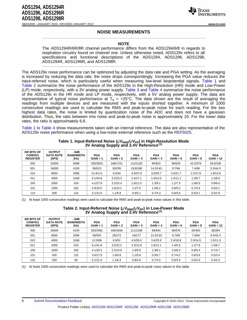
NOISE MEASUREMENTS
NOTEThe ADS1294R/6R/8R channel performance differs from the ADS1294/6/8 in regards torespiration circuitry found on channel one. Unless otherwise noted, ADS129x refers to allspecifications and functional descriptions of the ADS1294, ADS1296, ADS1298,ADS1294R, ADS1296R, and ADS1298R.
The ADS129x noise performance can be optimized by adjusting the data rate and PGA setting. As the averagingis increased by reducing the data rate, the noise drops correspondingly. Increasing the PGA value reduces theinput-referred noise, which is particularly useful when measuring low-level biopotential signals. Table 1 andTable 2 summarize the noise performance of the ADS129x in the High-Resolution (HR) mode and Low-Power(LP) mode, respectively, with a 3V analog power supply. Table 3 and Table 4 summarize the noise performanceof the ADS129x in the HR mode and LP mode, respectively, with a 5V analog power supply. The data arerepresentative of typical noise performance at TA = +25°C. The data shown are the result of averaging thereadings from multiple devices and are measured with the inputs shorted together. A minimum of 1000consecutive readings are used to calculate the RMS and peak-to-peak noise for each reading. For the twohighest data rates, the noise is limited by quantization noise of the ADC and does not have a gaussiandistribution. Thus, the ratio between rms noise and peak-to-peak noise is approximately 10. For the lower datarates, the ratio is approximately 6.6.
Table 1 to Table 4 show measurements taken with an internal reference. The data are also representative of theADS129x noise performance when using a low-noise external reference such as the REF5025.
Table 1. Input-Referred Noise (μVRMS/μVPP) in High-Resolution Mode3V Analog Supply and 2.4V Reference (1)
DR BITS OF OUTPUT –3dBCONFIG1 DATA RATE BANDWIDTH PGA PGA PGA PGA PGA PGA PGA
REGISTER (SPS) (Hz) GAIN = 1 GAIN = 2 GAIN = 3 GAIN = 4 GAIN = 6 GAIN = 8 GAIN = 12
000 32000 8398 335/3553 168/1701 112/1100 85/823 58/529 42.5/378 28.6/248
001 16000 4193 56/613 28/295 18.8/188 14.3/143 9.7/94 7.4/69 5.2/44.3
010 8000 2096 12.4/111 6.5/54 4.5/37.9 3.5/29.7 2.6/21.7 2.2/17.8 1.8/13.8
011 4000 1048 6.1/44.8 3.2/23.3 2.4/17.1 1.9/14.0 1.5/11.1 1.3/9.7 1.2/8.5
100 2000 524 4.1/27.8 2.2/15.4 1.6/11.0 1.3/9.1 1.1/7.3 1.0/6.5 0.9/6.0
101 1000 262 2.9/19.0 1.6/10.1 1.2/7.5 1.0/6.2 0.8/5.0 0.7/4.6 0.6/4.1
110 500 131 2.1/12.5 1.1/6.8 0.9/5.1 0.7/4.3 0.6/3.5 0.5/3.1 0.5/2.9
(1) At least 1000 consecutive readings were used to calculate the RMS and peak-to-peak noise values in this table.
Table 2. Input-Referred Noise (μVRMS/μVPP) in Low-Power Mode3V Analog Supply and 2.4V Reference (1)
DR BITS OF OUTPUT –3dBCONFIG1 DATA RATE BANDWIDTH PGA PGA PGA PGA PGA PGA PGA
REGISTER (SPS) (Hz) GAIN = 1 GAIN = 2 GAIN = 3 GAIN = 4 GAIN = 6 GAIN = 8 GAIN = 12
000 16000 4193 333/3481 166/1836 111/1168 84/834 56/576 42/450 28/284
001 8000 2096 56/554 28/272 19/177 14.3/133 9.7/85 7.4/64 5.0/42.4
010 4000 1048 12.5/99 6.5/51 4.5/35.0 3.4/25.9 2.4/18.8 2.0/14.5 1.5/11.3
011 2000 524 6.1/41.8 3.2/22.2 2.3/15.9 1.8/12.1 1.4/9.3 1.2/7.8 1.0/6.7
100 1000 262 4.1/26.3 2.2/14.6 1.6/9.9 1.3/8.1 1.0/6.2 0.8/5.4 0.7/4.7
101 500 131 3.0/17.9 1.6/9.8 1.1/6.8 0.9/5.7 0.7/4.2 0.6/3.6 0.5/3.4
110 250 65 2.1/11.9 1.1/6.3 0.8/4.6 0.7/4.0 0.5/3.0 0.5/2.6 0.4/2.4
(1) At least 1000 consecutive readings were used to calculate the RMS and peak-to-peak noise values in this table.
8 Submit Documentation Feedback Copyright © 2010–2012, Texas Instruments Incorporated
Product Folder Link(s): ADS1294 ADS1294R ADS1296 ADS1296R ADS1298 ADS1298R
ADS1294, ADS1294RADS1296, ADS1296RADS1298, ADS1298R
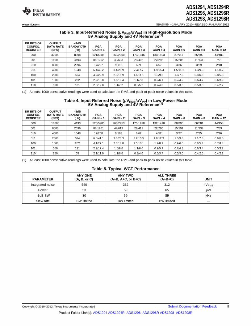
www.ti.com SBAS459I –JANUARY 2010–REVISED JANUARY 2012
Table 3. Input-Referred Noise (μVRMS/μVPP) in High-Resolution Mode5V Analog Supply and 4V Reference (1)
DR BITS OF OUTPUT –3dBCONFIG1 DATA RATE BANDWIDTH PGA PGA PGA PGA PGA PGA PGA
REGISTER (SPS) (Hz) GAIN = 1 GAIN = 2 GAIN = 3 GAIN = 4 GAIN = 6 GAIN = 8 GAIN = 12
000 32000 8398 521/5388 260/2900 173/1946 130/1403 87/917 65/692 44/483
001 16000 4193 86/1252 43/633 29/402 22/298 15/206 11/141 7/91
010 8000 2096 17/207 9/112 6/71 4/57 3/36 3/29 2/18
011 4000 1048 6.4/48.2 3.4/25.9 2.417.7 1.9/15.4 1.5/11.2 1.3/9.6 1.1/8.2
100 2000 524 4.2/29.9 2.3/15.9 1.6/11.1 1.3/9.3 1.0/7.5 0.9/6.6 0.8/5.8
101 1000 262 2.9/18.8 1.6/10.4 1.1/7.8 0.9/6.1 0.7/4.9 0.6/4.7 0.6/3.9
110 500 131 2.0/12.8 1.1/7.2 0.8/5.2 0.7/4.0 0.5/3.3 0.5/3.3 0.4/2.7
(1) At least 1000 consecutive readings were used to calculate the RMS and peak-to-peak noise values in this table.
Table 4. Input-Referred Noise (μVRMS/μVPP) in Low-Power Mode5V Analog Supply and 4V Reference (1)
DR BITS OF OUTPUT –3dBCONFIG1 DATA RATE BANDWIDTH PGA PGA PGA PGA PGA PGA PGA
REGISTER (SPS) (Hz) GAIN = 1 GAIN = 2 GAIN = 3 GAIN = 4 GAIN = 6 GAIN = 8 GAIN = 12
000 16000 4193 526/5985 263/2953 175/1918 132/1410 88/896 66/681 44/458
001 8000 2096 88/1201 44/619 29/411 22/280 15/191 11/139 7/83
010 4000 1048 17/208 9/103 6/62 4/52 3/37 2/25 2/16
011 2000 524 6.0/41.1 3.3/23.3 2.2/15.5 1.8/12.3 1.3/9.8 1.1/7.8 0.9/6.5
100 1000 262 4.1/27.1 2.3/14.8 1.5/10.1 1.2/8.1 0.9/6.0 0.8/5.4 0.7/4.4
101 500 131 2.9/17.4 1.6/9.6 1.1/6.6 0.9/5.9 0.7/4.3 0.6/3.4 0.5/3.2
110 250 65 2.1/11.9 1.1/6.6 0.8/4.6 0.6/3.7 0.5/3.0 0.4/2.5 0.4/2.2
(1) At least 1000 consecutive readings were used to calculate the RMS and peak-to-peak noise values in this table.
Table 5. Typical WCT Performance
ANY ONE ANY TWO ALL THREEPARAMETER (A, B, or C) (A+B, A+C, or B+C) (A+B+C) UNIT
Integrated noise 540 382 312 nVRMS
Power 53 59 65 μW
–3dB BW 30 59 89 kHz
Slew rate BW limited BW limited BW limited —
Copyright © 2010–2012, Texas Instruments Incorporated Submit Documentation Feedback 9
Product Folder Link(s): ADS1294 ADS1294R ADS1296 ADS1296R ADS1298 ADS1298R

1
2
3
4
5
6
7
8
H G F E D C B A
IN8PIN7PIN6PIN5PIN4PIN3PIN2PIN1P
IN8NIN7NIN6NIN5NIN4NIN3NIN2NIN1N
RLDINRLDOUTRLDINVWCT
TESTP_PACE_OUT1
TESTN_PACE_OUT2VCAP4VREFP
AVDDAVDDRLDREFAVSSRESV1RESP_MODN
RESP_MODPVREFN
AVSSAVSSAVSSAVSSGPIO4GPIO1PWDNVCAP1
AVDDAVDDAVDDDRDYGPIO3DAISY_INRESETVCAP2
AVDD1VCAP3DGNDDGNDGPIO2CSSTARTDGND
AVSS1CLKSELDVDDDVDDDOUTSCLKCLKDIN
ADS1294, ADS1294RADS1296, ADS1296RADS1298, ADS1298RSBAS459I –JANUARY 2010–REVISED JANUARY 2012 www.ti.com
PIN CONFIGURATIONS
ZXG PACKAGEBGA-64
(TOP VIEW, SOLDER BUMPS ON BOTTOM SIDE)
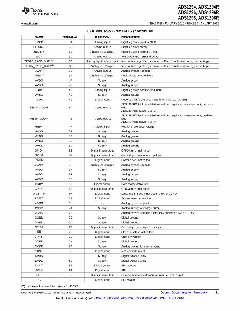
BGA PIN ASSIGNMENTSNAME TERMINAL FUNCTION DESCRIPTION
IN8P (1) 1A Analog input Differential analog positive input 8 (ADS1298/8R)
IN7P (1) 1B Analog input Differential analog positive input 7 (ADS1298/8R)
IN6P (1) 1C Analog input Differential analog positive input 6 (ADS1296/8/6R/8R)
IN5P (1) 1D Analog input Differential analog positive input 5 (ADS1296/8/6R/8R)
IN4P (1) 1E Analog input Differential analog positive input 4
IN3P (1) 1F Analog input Differential analog positive input 3
IN2P (1) 1G Analog input Differential analog positive input 2
IN1P (1) 1H Analog input Differential analog positive input 1
IN8N (1) 2A Analog input Differential analog negative input 8 (ADS1298/8R)
IN7N (1) 2B Analog input Differential analog negative input 7 (ADS1298/8R)
IN6N (1) 2C Analog input Differential analog negative input 6 (ADS1296/8/6R/8R)
IN5N (1) 2D Analog input Differential analog negative input 5 (ADS1296/8/6R/8R)
IN4N (1) 2E Analog input Differential analog negative input 4
IN3N (1) 2F Analog input Differential analog negative input 3
IN2N (1) 2G Analog input Differential analog negative input 2
IN1N (1) 2H Analog input Differential analog negative input 1
(1) Connect unused terminals to AVDD.
10 Submit Documentation Feedback Copyright © 2010–2012, Texas Instruments Incorporated
Product Folder Link(s): ADS1294 ADS1294R ADS1296 ADS1296R ADS1298 ADS1298R
ADS1294, ADS1294RADS1296, ADS1296RADS1298, ADS1298R
www.ti.com SBAS459I –JANUARY 2010–REVISED JANUARY 2012
BGA PIN ASSIGNMENTS (continued)NAME TERMINAL FUNCTION DESCRIPTION
RLDIN (2) 3A Analog input Right leg drive input to MUX
RLDOUT 3B Analog output Right leg drive output
RLDINV 3C Analog input/output Right leg drive inverting input
WCT 3D Analog output Wilson Central Terminal output
TESTP_PACE_OUT1 (2) 3E Analog input/buffer output Internal test signal/single-ended buffer output based on register settings
TESTN_PACE_OUT2 (2) 3F Analog input/output Internal test signal/single-ended buffer output based on register settings
VCAP4 3G Analog output Analog bypass capacitor
VREFP 3H Analog input/output Positive reference voltage
AVDD 4A Supply Analog supply
AVDD 4B Supply Analog supply
RLDREF 4C Analog input Right leg drive noninverting input
AVSS 4D Supply Analog ground
RESV1 4E Digital input Reserved for future use; must tie to logic low (DGND).
ADS1294R/6R/8R: modulation clock for respiration measurement, negativeRESP_MODN 4F Analog output side.
ADS1294/6/8: leave floating.
ADS1294R/6R/8R: modulation clock for respiration measurement, positiveRESP_MODP 4G Analog output side.
ADS1294/6/8: leave floating.
VREFN 4H Analog input Negative reference voltage
AVSS 5A Supply Analog ground
AVSS 5B Supply Analog ground
AVSS 5C Supply Analog ground
AVSS 5D Supply Analog ground
GPIO4 5E Digital input/output GPIO4 in normal mode
GPIO1 5F Digital input/output General purpose input/output pin
PWDN 5G Digital input Power-down; active low
VCAP1 5H Analog input/output Analog bypass capacitor
AVDD 6A Supply Analog supply
AVDD 6B Supply Analog supply
AVDD 6C Supply Analog supply
DRDY 6D Digital output Data ready; active low
GPIO3 6E Digital input/output GPIO3 in normal mode
DAISY_IN 6F Digital input Daisy-chain input; if not used, short to DGND.
RESET 6G Digital input System reset; active low
VCAP2 6H — Analog bypass capacitor
AVDD1 7A Supply Analog supply for charge pump
VCAP3 7B — Analog bypass capacitor; internally generated AVDD + 1.9V.
DGND 7C Supply Digital ground
DGND 7D Supply Digital ground
GPIO2 7E Digital input/output General-purpose input/output pin
CS 7F Digital input SPI chip select; active low
START 7G Digital input Start conversion
DGND 7H Supply Digital ground
AVSS1 8A Supply Analog ground for charge pump
CLKSEL 8B Digital input Master clock select
DVDD 8C Supply Digital power supply
DVDD 8D Supply Digital power supply
DOUT 8E Digital output SPI data out
SCLK 8F Digital input SPI clock
CLK 8G Digital input/output External Master clock input or internal clock output.
DIN 8H Digital input SPI data in
(2) Connect unused terminals to AVDD.
Copyright © 2010–2012, Texas Instruments Incorporated Submit Documentation Feedback 11
Product Folder Link(s): ADS1294 ADS1294R ADS1296 ADS1296R ADS1298 ADS1298R
48
47
46
45
44
43
42
41
40
39
38
37
36
35
34
33
DVDD
GPIO4
GPIO3
GPIO2
DOUT
GPIO1
DAISY_IN
SCLK
START
CLK
DIN
DGND
DRDY
CS
RESET
PWDN
1
2
3
4
5
6
7
8
9
10
11
12
13
14
15
16
IN8N
IN8P
IN7N
IN7P
IN6N
IN6P
IN5N
IN5P
IN4N
IN4P
IN3N
IN3P
IN2N
IN2P
IN1N
IN1P
WC
T
RLD
OU
T
RLD
IN
RLD
INV
RLD
RE
F
AV
DD
AV
SS
AV
SS
AV
DD
VC
AP
3
AV
DD
1
AV
SS
1
CLK
SE
L
DG
ND
DV
DD
DG
ND
TE
ST
P_P
AC
E_O
UT
1
TE
ST
N_P
AC
E_O
UT
2
AV
DD
AV
SS
AV
DD
AV
DD
AV
SS
VR
EF
P
VR
EF
N
VC
AP
4
NC
VC
AP
1
NC
VC
AP
2
RE
SV
1
AV
SS
17
18
19
20
21
22
23
24
25
26
27
28
29
30
31
32
64
63
62
61
60
59
58
57
56
55
54
53
52
51
50
49
ADS1294, ADS1294RADS1296, ADS1296RADS1298, ADS1298RSBAS459I –JANUARY 2010–REVISED JANUARY 2012 www.ti.com
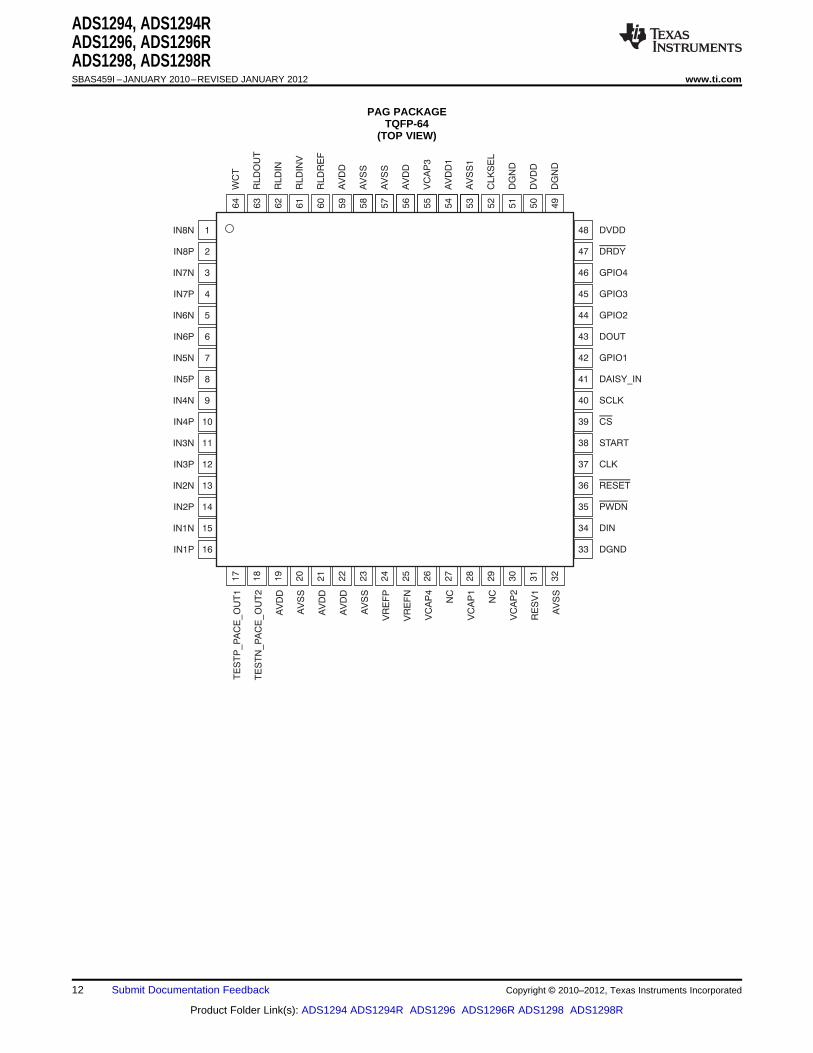
PAG PACKAGETQFP-64
(TOP VIEW)
12 Submit Documentation Feedback Copyright © 2010–2012, Texas Instruments Incorporated
Product Folder Link(s): ADS1294 ADS1294R ADS1296 ADS1296R ADS1298 ADS1298R
ADS1294, ADS1294RADS1296, ADS1296RADS1298, ADS1298R
www.ti.com SBAS459I –JANUARY 2010–REVISED JANUARY 2012
PAG PIN ASSIGNMENTSNAME PIN FUNCTION DESCRIPTION
IN8N (1) 1 Analog input Differential analog negative input 8 (ADS1298)
IN8P (1) 2 Analog input Differential analog positive input 8 (ADS1298)
IN7N (1) 3 Analog input Differential analog negative input 7 (ADS1298)
IN7P (1) 4 Analog input Differential analog positive input 7 (ADS1298)
IN6N (1) 5 Analog input Differential analog negative input 6 (ADS1296/8)
IN6P (1) 6 Analog input Differential analog positive input 6 (ADS1296/8)
IN5N (1) 7 Analog input Differential analog negative input 5 (ADS1296/8)
IN5P (1) 8 Analog input Differential analog positive input 5 (ADS1296/8)
IN4N (1) 9 Analog input Differential analog negative input 4
IN4P (1) 10 Analog input Differential analog positive input 4
IN3N (1) 11 Analog input Differential analog negative input 3
IN3P (1) 12 Analog input Differential analog positive input 3
IN2N (1) 13 Analog input Differential analog negative input 2
IN2P (1) 14 Analog input Differential analog positive input 2
IN1N (1) 15 Analog input Differential analog negative input 1
IN1P (1) 16 Analog input Differential analog positive input 1
TESTP_PACE_OUT1 (1) 17 Analog input/buffer output Internal test signal/single-ended buffer output based on register settings
TESTN_PACE_OUT2 (1) 18 Analog input/output Internal test signal/single-ended buffer output based on register settings
AVDD 19 Supply Analog supply
AVSS 20 Supply Analog ground
AVDD 21 Supply Analog supply
AVDD 22 Supply Analog supply
AVSS 23 Supply Analog ground
VREFP 24 Analog input/output Positive reference voltage
VREFN 25 Analog input Negative reference voltage
VCAP4 26 Analog output Analog bypass capacitor
NC 27 — No connection
VCAP1 28 — Analog bypass capacitor
NC 29 — No connection
VCAP2 30 — Analog bypass capacitor
RESV1 31 Digital input Reserved for future use; must tie to logic low (DGND).
AVSS 32 Supply Analog ground
DGND 33 Supply Digital ground
DIN 34 Digital input SPI data in
PWDN 35 Digital input Power-down; active low
RESET 36 Digital input System reset; active low
CLK 37 Digital input/output External Master clock input or internal clock output.
START 38 Digital input Start conversion
CS 39 Digital input SPI chip select; active low
SCLK 40 Digital input SPI clock
DAISY_IN 41 Digital input Daisy-chain input; if not used, short to DGND.
GPIO1 42 Digital input/output General-purpose input/output pin
DOUT 43 Digital output SPI data out
GPIO2 44 Digital input/output General-purpose input/output pin
GPIO3 45 Digital input/output General-purpose input/output pin
GPIO4 46 Digital input/output General-purpose input/output pin
DRDY 47 Digital output Data ready; active low
DVDD 48 Supply Digital power supply
DGND 49 Supply Digital ground
DVDD 50 Supply Digital power supply
(1) Connect unused terminals to AVDD.
Copyright © 2010–2012, Texas Instruments Incorporated Submit Documentation Feedback 13
Product Folder Link(s): ADS1294 ADS1294R ADS1296 ADS1296R ADS1298 ADS1298R
ADS1294, ADS1294RADS1296, ADS1296RADS1298, ADS1298RSBAS459I –JANUARY 2010–REVISED JANUARY 2012 www.ti.com
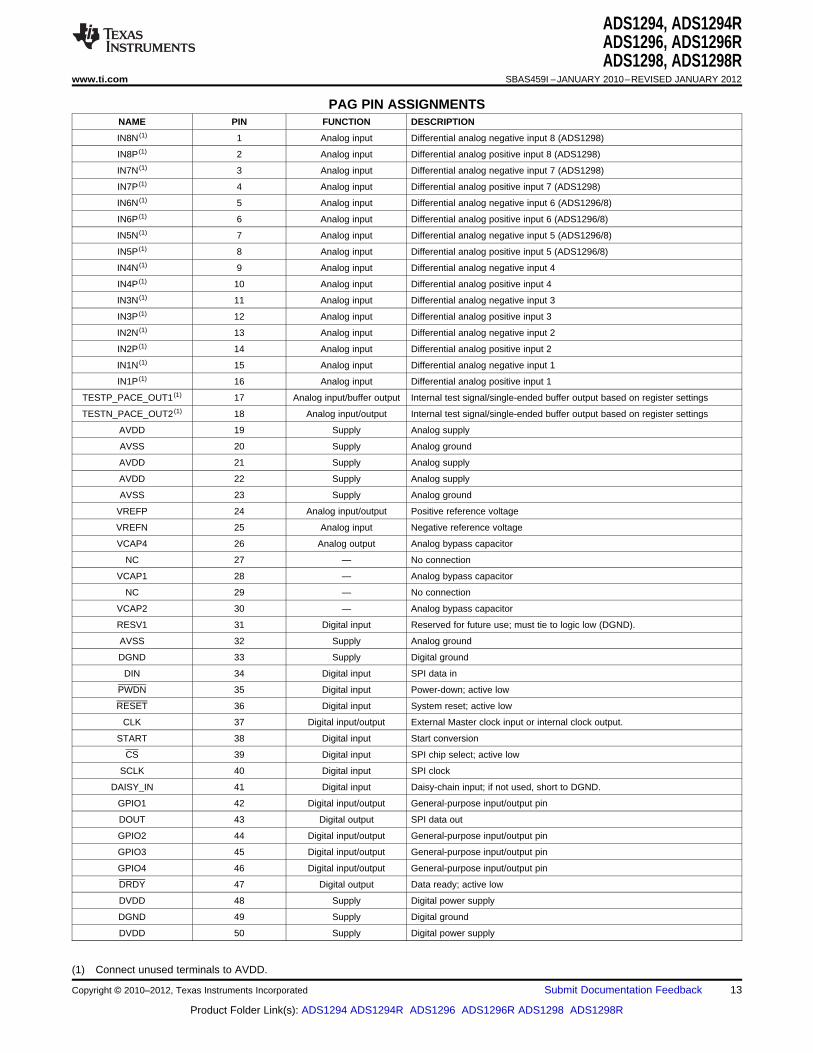
PAG PIN ASSIGNMENTS (continued)NAME PIN FUNCTION DESCRIPTION
DGND 51 Supply Digital ground
CLKSEL 52 Digital input Master clock select
AVSS1 53 Supply Analog ground
AVDD1 54 Supply Analog supply
VCAP3 55 Analog Analog bypass capacitor; internally generated AVDD + 1.9V.
AVDD 56 Supply Analog supply
AVSS 57 Supply Analog ground
AVSS 58 Supply Analog ground
AVDD 59 Supply Analog supply
RLDREF 60 Analog input Right leg drive noninverting input
RLDINV 61 Analog input/output Right leg drive inverting input
RLDIN (1) 62 Analog input Right leg drive input to MUX
RLDOUT 63 Analog output Right leg drive output
WCT 64 Analog output Wilson Central Terminal output
14 Submit Documentation Feedback Copyright © 2010–2012, Texas Instruments Incorporated
Product Folder Link(s): ADS1294 ADS1294R ADS1296 ADS1296R ADS1298 ADS1298R
1
CS
SCLK
DIN
DOUT
2 3 8 1 2 83
tCSSC
tDIST
tDIHD tDOHD
tCSH
tDOPD
tSPWH
tSPWL tSCCS
Hi-Z
tCSDOZtCSDOD
Hi-Z
tSCLK
tSDECODE
CLK
tCLK
D ISY_INA
DOUT
SCLK
MSBD1
tDISCK2ST
MSB
21 3 216 217 218
MSBD1LSB
tDISCK2HT
tDOPD
Don’t Care
LSBD1
219
ADS1294, ADS1294RADS1296, ADS1296RADS1298, ADS1298R
www.ti.com SBAS459I –JANUARY 2010–REVISED JANUARY 2012
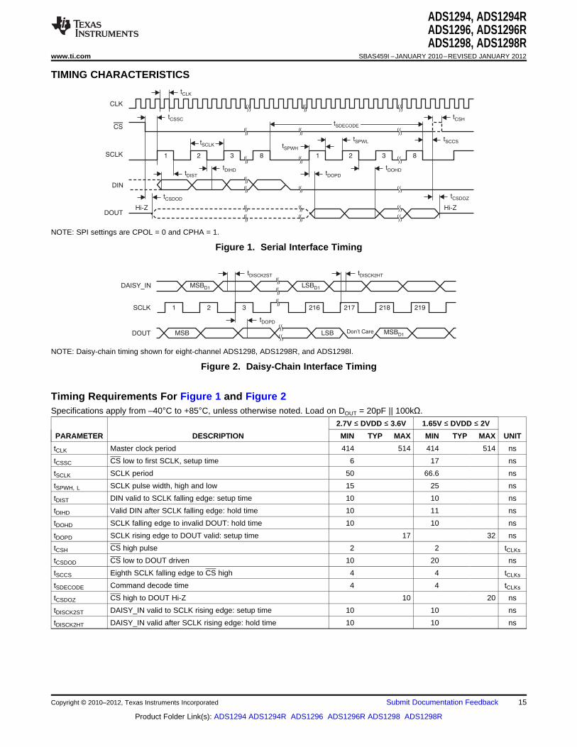
TIMING CHARACTERISTICS
NOTE: SPI settings are CPOL = 0 and CPHA = 1.
Figure 1. Serial Interface Timing
NOTE: Daisy-chain timing shown for eight-channel ADS1298, ADS1298R, and ADS1298I.
Figure 2. Daisy-Chain Interface Timing
Timing Requirements For Figure 1 and Figure 2Specifications apply from –40°C to +85°C, unless otherwise noted. Load on DOUT = 20pF || 100kΩ.
2.7V ≤ DVDD ≤ 3.6V 1.65V ≤ DVDD ≤ 2V
PARAMETER DESCRIPTION MIN TYP MAX MIN TYP MAX UNIT
tCLK Master clock period 414 514 414 514 ns
tCSSC CS low to first SCLK, setup time 6 17 ns
tSCLK SCLK period 50 66.6 ns
tSPWH, L SCLK pulse width, high and low 15 25 ns
tDIST DIN valid to SCLK falling edge: setup time 10 10 ns
tDIHD Valid DIN after SCLK falling edge: hold time 10 11 ns
tDOHD SCLK falling edge to invalid DOUT: hold time 10 10 ns
tDOPD SCLK rising edge to DOUT valid: setup time 17 32 ns
tCSH CS high pulse 2 2 tCLKs
tCSDOD CS low to DOUT driven 10 20 ns
tSCCS Eighth SCLK falling edge to CS high 4 4 tCLKs
tSDECODE Command decode time 4 4 tCLKs
tCSDOZ CS high to DOUT Hi-Z 10 20 ns
tDISCK2ST DAISY_IN valid to SCLK rising edge: setup time 10 10 ns
tDISCK2HT DAISY_IN valid after SCLK rising edge: hold time 10 10 ns
Copyright © 2010–2012, Texas Instruments Incorporated Submit Documentation Feedback 15
Product Folder Link(s): ADS1294 ADS1294R ADS1296 ADS1296R ADS1298 ADS1298R
3
2
1
0
1
2
3
-
-
-
Time (sec)
Input-
Refe
rred N
ois
e (
V)
m
1 20 103 4 5 6 7 8 9
Peak-to-Peak Over 10sec = 5 Vm
1600
1400
1200
1000
800
600
400
200
0
Input-Referred Noise ( V)m
Occu
rre
nce
s
-2
.88
-2
.35
-1
.85
-1
.35
-0
.84
-0
.34
0.1
7
1.1
7
2.1
8
0.6
7
1.6
8
2.408
2.406
2.404
2.402
2.4
2.398
2.396-40 85
Temperature ( C)°
Inte
rnal R
efe
rence (
V)
-15 10 6035
-130
125
120
115
110
105
100
95
90
85
-
-
-
-
-
-
-
-
-
10 1k
Frequency (Hz)
Co
mm
on-M
od
e R
eje
ctio
n R
atio
(d
B)
100
Gain = 1
Data Rate = 4kSPS
AIN = AVDD 0.3V to AVSS + 0.3V-
Gain = 2
Gain = 3
Gain = 4
Gain = 6
Gain = 8
Gain = 12
0.18
0.16
0.14
0.12
0.10
0.08
0.06
0.04
0.02
00.3 4.8
Input Voltage (V)
Inp
ut
Le
aka
ge
Cu
rre
nt
(nA
)
2.3
AVDD AVSS = 5V
PGA = 1
-
1.81.30.8 2.8 3.3 3.8 4.3
1200
1000
800
600
400
200
0-40 85
Temperature ( C)°
Le
aka
ge
Cu
rre
nt
(pA
)
3510-15 60
ADS1294, ADS1294RADS1296, ADS1296RADS1298, ADS1298RSBAS459I –JANUARY 2010–REVISED JANUARY 2012 www.ti.com
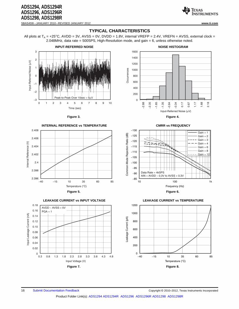
TYPICAL CHARACTERISTICSAll plots at TA = +25°C, AVDD = 3V, AVSS = 0V, DVDD = 1.8V, internal VREFP = 2.4V, VREFN = AVSS, external clock =
2.048MHz, data rate = 500SPS, High-Resolution mode, and gain = 6, unless otherwise noted.
INPUT-REFERRED NOISE NOISE HISTOGRAM
Figure 3. Figure 4.
INTERNAL REFERENCE vs TEMPERATURE CMRR vs FREQUENCY
Figure 5. Figure 6.
LEAKAGE CURRENT vs INPUT VOLTAGE LEAKAGE CURRENT vs TEMPERATURE
Figure 7. Figure 8.
16 Submit Documentation Feedback Copyright © 2010–2012, Texas Instruments Incorporated
Product Folder Link(s): ADS1294 ADS1294R ADS1296 ADS1296R ADS1298 ADS1298R
110
105
100
95
90
85
80
75
7010 1k
Frequency (Hz)
Po
we
r-S
up
ply
Re
jectio
n R
atio
(d
B)
100
Data Rate = 4kSPS
Gain = 2
Gain = 4
Gain = 1
Gain = 12
Gain = 3
Gain = 8
Gain = 6
-105
100
95
90
85
80
75
70
-
-
-
-
-
-
-
10 1k
Frequency (Hz)
Tota
l H
arm
onic
Dis
tort
ion (
dB
)
100
Data Rate = 4kSPS
AIN = 0.5dBFS
Gain = 1
Gain = 2
Gain = 4
Gain = 12
Gain = 3
Gain = 8
Gain = 6
8
6
4
2
0
2
4
6
8
-
-
-
-
-1 1
Input Range (Normalized to Full-Scale)
Inte
gra
l N
onlin
earity
(ppm
)
-0.5 0.50
-40 C°
-20 C°
0 C°
+25 C°
+40 C°
+60 C°
+70 C°
+85 C°
10
8
6
4
2
0
2
4
6
8
10
-
-
-
-
-
Input (Normalized to Full-Scale)
Inte
gra
l N
onlin
earity
(ppm
)
-0.8-1.0 1.0-0.2 0.2 0.6-0.6 0.8-0.4 0 0.4
Gain = 6Gain = 8Gain = 12
Gain = 1Gain = 2Gain = 3Gain = 4
0
20
40
60
80
100
120
140
160
180
-
-
-
-
-
-
-
-
-
Frequency (Hz)
Am
plit
ude (
dB
FS
)
500 250100 150 200
PGA Gain = 1
THD = 102dB
SNR = 115dB
f = 500SPS
f = External Clock
-
DR
CLK
0
20
40
60
80
100
120
140
160
180
-
-
-
-
-
-
-
-
-
Frequency (kHz)
Am
plit
ude (
dB
FS
)
20 164 6 8
PGA Gain = 6
THD = 104dB
SNR = 74.5dB
-
f = 32kSPSDR
10 12 14
ADS1294, ADS1294RADS1296, ADS1296RADS1298, ADS1298R
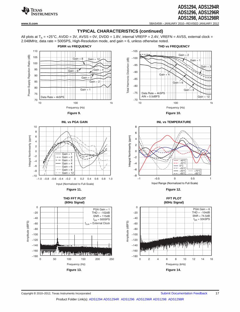
www.ti.com SBAS459I –JANUARY 2010–REVISED JANUARY 2012
TYPICAL CHARACTERISTICS (continued)All plots at TA = +25°C, AVDD = 3V, AVSS = 0V, DVDD = 1.8V, internal VREFP = 2.4V, VREFN = AVSS, external clock =2.048MHz, data rate = 500SPS, High-Resolution mode, and gain = 6, unless otherwise noted.
PSRR vs FREQUENCY THD vs FREQUENCY
Figure 9. Figure 10.
INL vs PGA GAIN INL vs TEMPERATURE
Figure 11. Figure 12.
THD FFT PLOT FFT PLOT(60Hz Signal) (60Hz Signal)
Figure 13. Figure 14.
Copyright © 2010–2012, Texas Instruments Incorporated Submit Documentation Feedback 17
Product Folder Link(s): ADS1294 ADS1294R ADS1296 ADS1296R ADS1298 ADS1298R

800
700
600
500
400
300
200
100
01 12
PGA Gain
Offse
t (
V)
m
8642 109753 11
70
60
50
40
30
20
10
0
-0.5
3
Error (%)
Num
ber
of B
ins
-0.4
1
-0.1
8
0.0
6
0.3
0
0.5
4
0.6
6
0.4
2
0.1
8
-0.0
6
-0.2
9
Data From 31 Devices, Two Lots
80
70
60
50
40
30
20
10
0
-2
0
Threshold Error (mV)
Nu
mb
er
of
Bin
s
-1
5 0
10
20
30
35
25
155
-1
0
Data From 31 Devices, Two Lots120
100
80
60
40
20
0
-2
.70
Error in Current Magnitude (nA)
Nu
mb
er
of
Bin
s
-2
.14
-1
.01
0.1
2
1.2
4
2.3
7
2.9
3
1.8
0
0.6
8
-0
.45
-1
.57
Data From 31 Devices, Two Lots
Current Setting = 24nA
17.5
15.5
13.5
11.5
9.5
7.5
5.5
3.5
1.5
Number of Channels Disabled
Pow
er
(mW
)
10 84 62 3 5 7
AVDD = 3V
AVDD = 5V
40
30
20
10
0
10
20
30
40
50
-
-
-
-
-
Input Range (Normalized to Full-Scale)
Inte
gra
l N
onlin
earity
(ppm
)
-0.8-1 1-0.2 0.2-0.6 -0.4 0 0.4 0.80.6
Channel 1Channel 2Channel 3Channel 4Channel 5Channel 6Channel 7Channel 8
ADS1294, ADS1294RADS1296, ADS1296RADS1298, ADS1298RSBAS459I –JANUARY 2010–REVISED JANUARY 2012 www.ti.com
TYPICAL CHARACTERISTICS (continued)All plots at TA = +25°C, AVDD = 3V, AVSS = 0V, DVDD = 1.8V, internal VREFP = 2.4V, VREFN = AVSS, external clock =2.048MHz, data rate = 500SPS, High-Resolution mode, and gain = 6, unless otherwise noted.
OFFSET vs PGA GAIN(ABSOLUTE VALUE) TEST SIGNAL AMPLITUDE ACCURACY
Figure 15. Figure 16.
LEAD-OFF CURRENT SOURCE ACCURACYLEAD-OFF COMPARATOR THRESHOLD ACCURACY DISTRIBUTION
Figure 17. Figure 18.
ADS1294R/6R/8R NONLINEARITY ADS1298/8R CHANNEL POWER
Figure 19. Figure 20.
18 Submit Documentation Feedback Copyright © 2010–2012, Texas Instruments Incorporated
Product Folder Link(s): ADS1294 ADS1294R ADS1296 ADS1296R ADS1298 ADS1298R
110
105
100
95
90
85
80
75
70
65
60
Channel
Tota
l H
arm
onic
Dis
tort
ion (
dB
c)
1 84 62 3 5 7
f = 10Hz, 0.5dBFS-IN
120
110
100
90
80
70
60
50
Input Amplitude (dBFS)
Sig
nal-to
-Nois
e R
atio (
dB
)
-50-60 -0.5-20 -5-40 -30 -12 -2
Internal Master Clock, AVDD = 3V
External Master Clock, AVDD = 3V
External Master Clock, AVDD = 5V
Internal Master Clock, AVDD = 5V
ADS1294, ADS1294RADS1296, ADS1296RADS1298, ADS1298R
www.ti.com SBAS459I –JANUARY 2010–REVISED JANUARY 2012
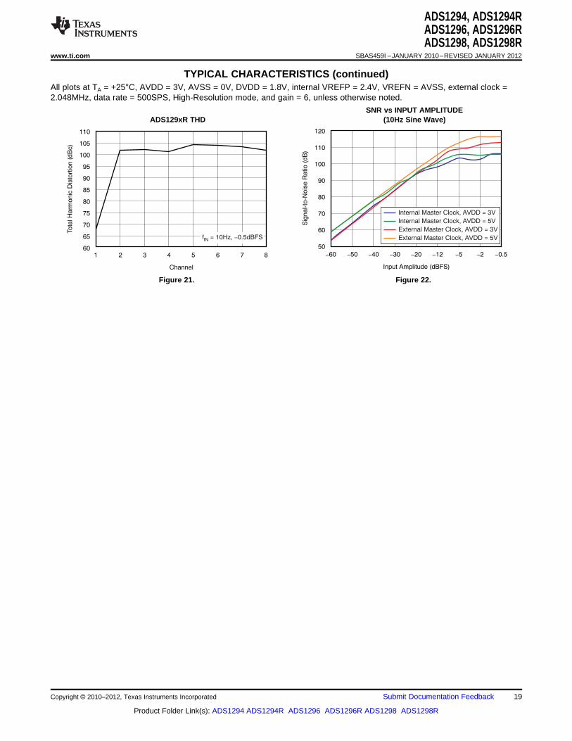
TYPICAL CHARACTERISTICS (continued)All plots at TA = +25°C, AVDD = 3V, AVSS = 0V, DVDD = 1.8V, internal VREFP = 2.4V, VREFN = AVSS, external clock =2.048MHz, data rate = 500SPS, High-Resolution mode, and gain = 6, unless otherwise noted.
SNR vs INPUT AMPLITUDEADS129xR THD (10Hz Sine Wave)
Figure 21. Figure 22.
Copyright © 2010–2012, Texas Instruments Incorporated Submit Documentation Feedback 19
Product Folder Link(s): ADS1294 ADS1294R ADS1296 ADS1296R ADS1298 ADS1298R
ADS1294, ADS1294RADS1296, ADS1296RADS1298, ADS1298RSBAS459I –JANUARY 2010–REVISED JANUARY 2012 www.ti.com
OVERVIEW
NOTEThe ADS1294R/6R/8R channel performance differs from the ADS1294/6/8 in regards torespiration circuitry found on channel one. Unless otherwise noted, ADS129x refers to allspecifications and functional descriptions of the ADS1294, ADS1296, ADS1298,ADS1294R, ADS1296R, and ADS1298R.
The ADS129x are low-power, multichannel, simultaneously-sampling, 24-bit delta-sigma (ΔΣ) analog-to-digitalconverters (ADCs) with integrated programmable gain amplifiers (PGAs). These devices integrate variousECG-specific functions that make them well-suited for scalable electrocardiogram (ECG),electroencephalography (EEG), and electromyography (EMG) applications. The devices can also be used inhigh-performance, multichannel data acquisition systems by powering down the ECG-specific circuitry.
The ADS129x have a highly programmable multiplexer that allows for temperature, supply, input short, and RLDmeasurements. Additionally, the multiplexer allows any of the input electrodes to be programmed as the patientreference drive. The PGA gain can be chosen from one of seven settings (1, 2, 3, 4, 6, 8, and 12). The ADCs inthe device offer data rates from 250SPS to 32kSPS. Communication to the device is accomplished using anSPI-compatible interface. The device provides four GPIO pins for general use. Multiple devices can besynchronized using the START pin.
The internal reference can be programmed to either 2.4V or 4V. The internal oscillator generates a 2.048MHzclock. The versatile right leg drive (RLD) block allows the user to choose the average of any combination ofelectrodes to generate the patient drive signal. Lead-off detection can be accomplished either by using apull-up/pull-down resistor or a current source/sink. An internal ac lead-off detection feature is also available. Thedevice supports both hardware PACE detection and software PACE detection. The Wilson Central Terminal(WCT) block can be used to generate the WCT point of the standard 12-lead ECG.
Additionally, the ADS1294R, ADS1296R, and ADS1298R provide options for an internal respiration modulatorand a demodulator circuit in the signal path of channel 1.
20 Submit Documentation Feedback Copyright © 2010–2012, Texas Instruments Incorporated
Product Folder Link(s): ADS1294 ADS1294R ADS1296 ADS1296R ADS1298 ADS1298R

DR
DY
CL
K
CL
KS
EL
STA
RT
MU
X
Oscill
ato
r
Po
we
r-S
up
ply
Sig
na
l
SP
I
DV
DD
DG
ND
RLD
INV
RL
DO
UT
RL
DR
EF
Le
ad
-Off
Excita
tio
nS
ou
rce
PA
CE
OU
T2
GP
IO1
GP
IO4
/RC
LK
O
GP
IO3
/RC
LK
O
RE
SP
CL
K
PA
CE
OU
T1
CS
SC
LK
DIN
DO
UT
RL
DIN
ADS1298/8RADS1296/6R/8/8R
GP
IO2
AV
DD
AV
SS
IN8
P
IN8
N
IN7
P
IN7
N
IN6
P
IN6
N
IN5
P
IN5
N
IN4
P
IN4
N
IN3
P
IN3
N
IN2
P
IN2
N
IN1
P
IN1
N
PG
A1
DS
AD
C1
PG
A2
PG
A3
PG
A4
PG
A5
PG
A6
PG
A7
PG
A8
EM
I
Filt
er
EM
I
Filt
er
EM
I
Filt
er
EM
I
Filt
er
EM
I
Filt
er
EM
I
Filt
er
EM
I
Filt
er
EM
I
Filt
er
Tem
pe
ratu
re S
en
so
r In
pu
t
RL
D
Am
plif
ier
PA
CE
Am
plif
ier
2
PA
CE
Am
plif
ier
1
WC
T
BC A
Fro
m
Wm
uxc
Fro
m
Wm
uxa
Fro
m
Wm
uxb
WC
T
Re
fere
nce
VR
EF
PV
RE
FN
Contr
ol
PW
DN
RE
SE
T
DS
AD
C2
DS
AD
C3
DS
AD
C4
DS
AD
C5
DS
AD
C6
DS
AD
C7
DS
AD
C8
AV
DD
1
AV
SS
1
Test
Sig
na
lIn
tern
al R
esp
ira
tio
n
Mo
du
lato
r
()
AD
S1
29
xR
RE
SP
DE
MO
DR
ES
P_
DE
MO
D_
EN
ADS129xR
ADS129xR
RE
SP
_M
OD
P
RE
SP
_M
OD
N
G =
0.4
G =
0.4
ADS1294, ADS1294RADS1296, ADS1296RADS1298, ADS1298R
www.ti.com SBAS459I –JANUARY 2010–REVISED JANUARY 2012
Figure 23. Functional Block Diagram
Copyright © 2010–2012, Texas Instruments Incorporated Submit Documentation Feedback 21
Product Folder Link(s): ADS1294 ADS1294R ADS1296 ADS1296R ADS1298 ADS1298R
MUX[2:0] = 101
TempPMUX[2:0] = 100
MvddP(1) MUX[2:0] = 011
From LoffP
MUX[2:0] = 000
MUX[2:0] = 110
MUX[2:0] = 001
To PgaP
To PgaNMUX[2:0] = 001
RLDIN
MUX[2:0] = 010RLD_MEAS
AND
MUX[2:0] = 111
VINP
VINNMUX[2:0] = 000
From LoffN
RLD_REF
MUX[2:0] = 010RLD_MEAS
AND
MvddN(1)
TempNMUX[2:0] = 100
MUX[2:0] = 101
ADS129x
MUX
TestP
TestN
TESTP_PACE_OUT1
INT_TEST
INT_TEST
TESTN_PACE_OUT2
INT_TEST
INT_TEST
MUX[2:0] = 011
EMI
Filter
(AVDD + AVSS)
2
ADS1294, ADS1294RADS1296, ADS1296RADS1298, ADS1298RSBAS459I –JANUARY 2010–REVISED JANUARY 2012 www.ti.com
THEORY OF OPERATION
This section discusses the details of the ADS129x internal functional elements. The analog blocks are reviewedfirst, followed by the digital interface. Blocks implementing ECG-specific functions are covered in the end.
Throughout this document, fCLK denotes the frequency of the signal at the CLK pin, tCLK denotes the period of thesignal at the CLK pin, fDR denotes the output data rate, tDR denotes the time period of the output data, and fMODdenotes the frequency at which the modulator samples the input.
EMI FILTER
An RC filter at the input acts as an EMI filter on all of the channels. The –3dB filter bandwidth is approximately3MHz.
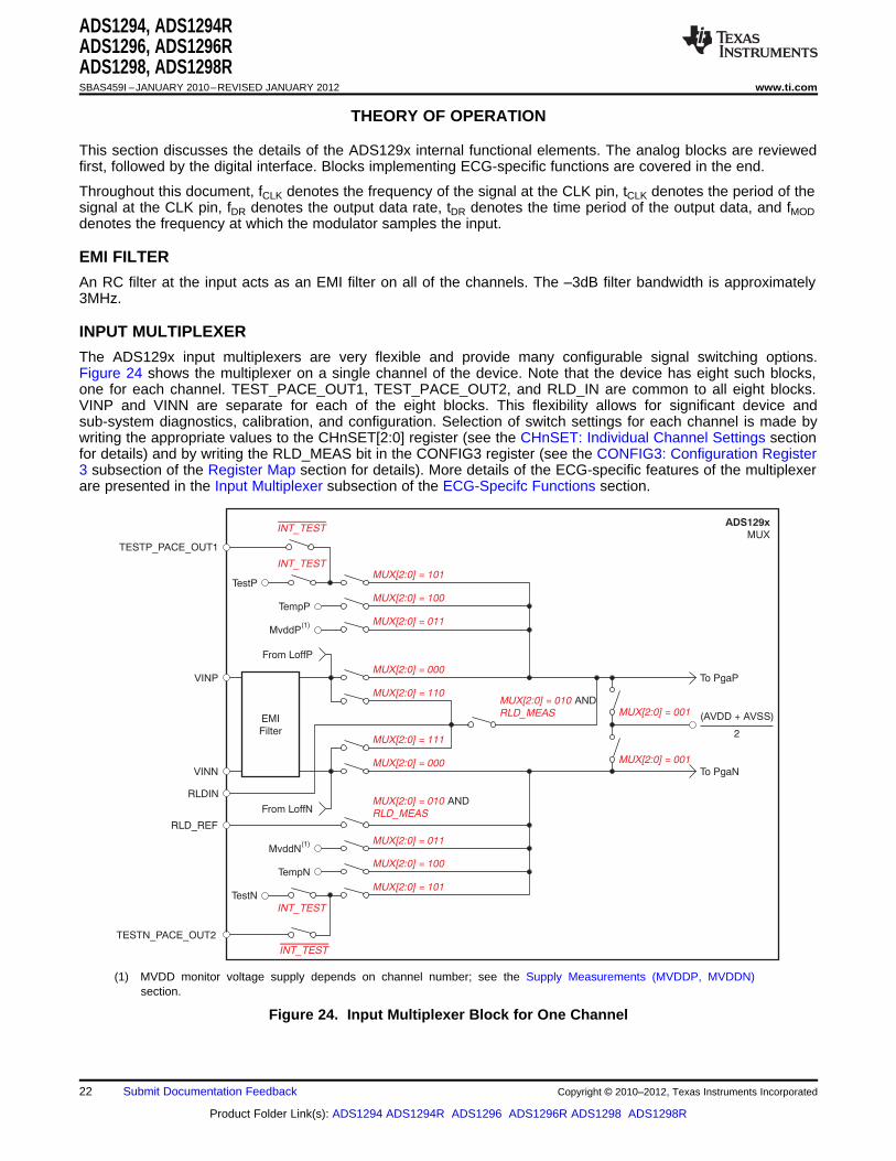
INPUT MULTIPLEXER
The ADS129x input multiplexers are very flexible and provide many configurable signal switching options.Figure 24 shows the multiplexer on a single channel of the device. Note that the device has eight such blocks,one for each channel. TEST_PACE_OUT1, TEST_PACE_OUT2, and RLD_IN are common to all eight blocks.VINP and VINN are separate for each of the eight blocks. This flexibility allows for significant device andsub-system diagnostics, calibration, and configuration. Selection of switch settings for each channel is made bywriting the appropriate values to the CHnSET[2:0] register (see the CHnSET: Individual Channel Settings sectionfor details) and by writing the RLD_MEAS bit in the CONFIG3 register (see the CONFIG3: Configuration Register3 subsection of the Register Map section for details). More details of the ECG-specific features of the multiplexerare presented in the Input Multiplexer subsection of the ECG-Specifc Functions section.
(1) MVDD monitor voltage supply depends on channel number; see the Supply Measurements (MVDDP, MVDDN)section.
Figure 24. Input Multiplexer Block for One Channel
22 Submit Documentation Feedback Copyright © 2010–2012, Texas Instruments Incorporated
Product Folder Link(s): ADS1294 ADS1294R ADS1296 ADS1296R ADS1298 ADS1298R
Temperature ( C) =°Temperature Reading ( V) 145,300 Vm - m
490 V/ Cm °
+ 25 C°
2x
1x
1x
8x
AVDD
AVSS
Temperature Sensor Monitor
To MUX TempP
To MUX TempN
ADS1294, ADS1294RADS1296, ADS1296RADS1298, ADS1298R
www.ti.com SBAS459I –JANUARY 2010–REVISED JANUARY 2012
Device Noise Measurements
Setting CHnSET[2:0] = 001 sets the common-mode voltage of (AVDD – AVSS)/2 to both inputs of the channel.This setting can be used to test the inherent noise of the device in the user system.
Test Signals (TestP and TestN)
Setting CHnSET[2:0] = 101 provides internally-generated test signals for use in sub-system verification atpower-up. This functionality allows the entire signal chain to be tested out. Although the test signals are similar tothe CAL signals described in the IEC60601-2-51 specification, this feature is not intended for use in compliancetesting.
Control of the test signals is accomplished through register settings (see the CONFIG2: Configuration Register 2subsection in the Register Map section for details). TEST_AMP controls the signal amplitude and TEST_FREQcontrols switching at the required frequency.
The test signals are multiplexed and transmitted out of the device at the TESTP_PACE_OUT1 andTESTN_PACE_OUT2 pins. A bit register (CONFIG2.INT_TEST = 0) deactivates the internal test signals so thatthe test signal can be driven externally. This feature allows the calibration of multiple devices with the samesignal. The test signal feature cannot be used in conjunction with the external hardware PACE feature (see theExternal Hardware Approach subsection of the ECG-Specific Functions section for details).
Auxiliary Differential Input (TESTP_PACE_OUT1, TESTN_PACE_OUT2)
When hardware PACE detect is not used, the TESTP_PACE_OUT1 and TESPN_PACE_OUT2 signals can beused as a multiplexed differential input channel. These inputs can be multiplexed to any of the eight channels.The performance of the differential input signal fed through these pins is identical to the normal channelperformance.
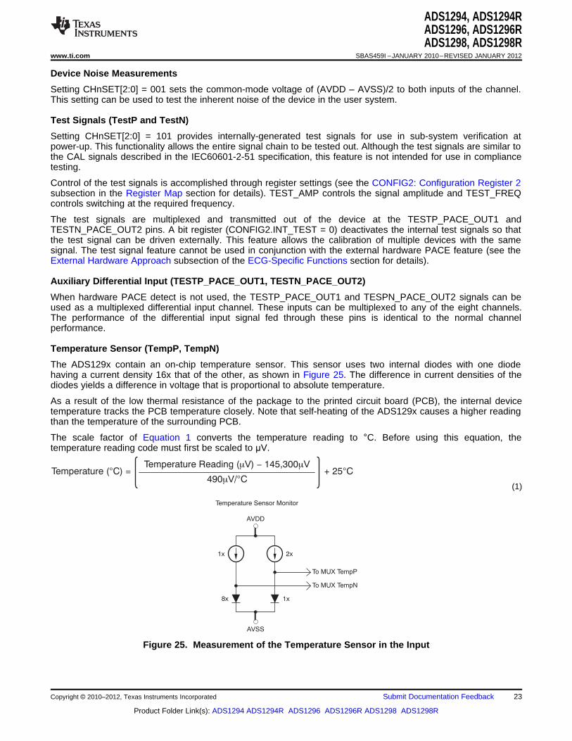
Temperature Sensor (TempP, TempN)
The ADS129x contain an on-chip temperature sensor. This sensor uses two internal diodes with one diodehaving a current density 16x that of the other, as shown in Figure 25. The difference in current densities of thediodes yields a difference in voltage that is proportional to absolute temperature.
As a result of the low thermal resistance of the package to the printed circuit board (PCB), the internal devicetemperature tracks the PCB temperature closely. Note that self-heating of the ADS129x causes a higher readingthan the temperature of the surrounding PCB.
The scale factor of Equation 1 converts the temperature reading to °C. Before using this equation, thetemperature reading code must first be scaled to μV.
(1)
Figure 25. Measurement of the Temperature Sensor in the Input
Copyright © 2010–2012, Texas Instruments Incorporated Submit Documentation Feedback 23
Product Folder Link(s): ADS1294 ADS1294R ADS1296 ADS1296R ADS1298 ADS1298R

ADS1298- V to
+1/2VREF
REF
1/2
Common
Voltage
Single-Ended Input
ADS1298
V
peak-to-peakREF
V
peak-to-peakREF
Common
Voltage
Differential Input
ADS1294, ADS1294RADS1296, ADS1296RADS1298, ADS1298RSBAS459I –JANUARY 2010–REVISED JANUARY 2012 www.ti.com
Supply Measurements (MVDDP, MVDDN)
Setting CHnSET[2:0] = 011 sets the channel inputs to different supply voltages of the device. For channels 1, 2,5, 6, 7, and 8, (MVDDP – MVDDN) is [0.5 × (AVDD – AVSS)]; for channel 3 and for channel 4, (MVDDP –MVDDN) is DVDD/4. Note that to avoid saturating the PGA while measuring power supplies, the gain must beset to '1'. For example, if AVDD = 2.5V and AVSS = –2.5V, then the measurement result would be 2.5V.
Lead-Off Excitation Signals (LoffP, LoffN)
The lead-off excitation signals are fed into the multiplexer before the switches. The comparators that detect thelead-off condition are also connected to the multiplexer block before the switches. For a detailed description ofthe lead-off block, refer to the Lead-Off Detection subsection in the ECG-Specific Functions section.
Auxiliary Single-Ended Input
The RLD_IN pin is primarily used for routing the right leg drive signal to any of the electrodes in case the right legdrive electrode falls off. However, the RLD_IN pin can be used as a multiple single-ended input channel. Thesignal at the RLD_IN pin can be measured with respect to the voltage at the RLD_REF pin using any of the eightchannels. This measurement is done by setting the channel multiplexer setting to '010' and the RLD_MEAS bit ofthe CONFIG3 register to '1'.
ANALOG INPUT
The analog input to the ADS1298 is fully differential. Assuming PGA = 1, the differential input (INP – INN) canspan between –VREF to +VREF. Note that the the absolute range for INP and INN must be between AVSS – 0.3Vand AVDD + 0.3V. Refer to Table 8 for an explanation of the correlation between the analog input and the digitalcodes. There are two general methods of driving the analog input of the ADS1298: single-ended or differential,as shown in Figure 26 and Figure 27. Note that INP and INN are 180°C out-of-phase in the differential inputmethod. When the input is single-ended, the INN input is held at the common-mode voltage, preferably atmid-supply. The INP input swings around the same common voltage and the peak-to-peak amplitude is the(common-mode + 1/2VREF) and the (common-mode – 1/2VREF). When the input is differential, the common-modeis given by (INP + INN)/2. Both the INP and INN inputs swing from (common-mode + 1/2VREF tocommon-mode – 1/2VREF). For optimal performance, it is recommended that the ADS1298 devices be used in adifferential configuration.
Figure 26. Methods of Driving the ADS1298: Single-Ended or Differential
24 Submit Documentation Feedback Copyright © 2010–2012, Texas Instruments Incorporated
Product Folder Link(s): ADS1294 ADS1294R ADS1296 ADS1296R ADS1298 ADS1298R
CM + 1/2VREF
+1/2VREF
- VREF1/2
Single-Ended Inputst
INPCM Voltage
CM V- REF1/2
CM + 1/2VREF
Differential Inputs
t
INP
INN
CM Voltage
CM 1/2VREF-
+VREF
-VREF
Common-Mode Voltage (Differential Mode) =(INP) + (INN)
2, Common-Mode Voltage (Single-Ended Mode) = INN.
INN = CM Voltage
Input Range (Differential Mode) = (AINP AINN) = V ( V ) = 2V .- REF REF- - REF
PgaP
R
50kW
2
R
20k
(for Gain = 6)
W
1
R
50kW
2
From MuxP
PgaN
From MuxN
To ADC
ADS1294, ADS1294RADS1296, ADS1296RADS1298, ADS1298R
www.ti.com SBAS459I –JANUARY 2010–REVISED JANUARY 2012
Figure 27. Using the ADS1298 in the Single-Ended and Differential Input Modes
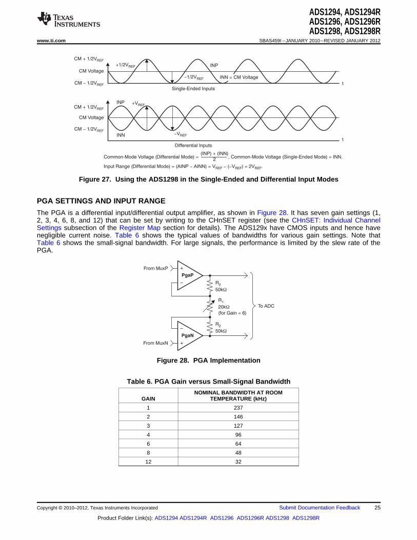
PGA SETTINGS AND INPUT RANGE
The PGA is a differential input/differential output amplifier, as shown in Figure 28. It has seven gain settings (1,2, 3, 4, 6, 8, and 12) that can be set by writing to the CHnSET register (see the CHnSET: Individual ChannelSettings subsection of the Register Map section for details). The ADS129x have CMOS inputs and hence havenegligible current noise. Table 6 shows the typical values of bandwidths for various gain settings. Note thatTable 6 shows the small-signal bandwidth. For large signals, the performance is limited by the slew rate of thePGA.
Figure 28. PGA Implementation
Table 6. PGA Gain versus Small-Signal Bandwidth
NOMINAL BANDWIDTH AT ROOMGAIN TEMPERATURE (kHz)
1 237
2 146
3 127
4 96
6 64
8 48
12 32
Copyright © 2010–2012, Texas Instruments Incorporated Submit Documentation Feedback 25
Product Folder Link(s): ADS1294 ADS1294R ADS1296 ADS1296R ADS1298 ADS1298R

AVDD 0.2- -
Gain VMAX_DIFF
2> CM > AVSS + 0.2 +
Gain VMAX_DIFF
2
Max (INP INN) <-
VREF
GainFull-Scale Range =
±VREF
Gain; =
2VREF
Gain
−160−150−140−130−120−110−100
−90−80−70−60−50−40−30−20−10
0
0.001 0.01 0.1 1Normalized Frequency (fIN/fMOD)
Pow
er S
pect
ral D
ensi
ty (
dB)
G001
ADS1294, ADS1294RADS1296, ADS1296RADS1298, ADS1298RSBAS459I –JANUARY 2010–REVISED JANUARY 2012 www.ti.com
The resistor string of the PGA that implements the gain has 120kΩ of resistance for a gain of 6. This resistanceprovides a current path across the outputs of the PGA in the presence of a differential input signal. This currentis in addition to the quiescent current specified for the device in the presence of a differential signal at the input.
Input Common-Mode Range
The usable input common-mode range of the front end depends on various parameters, including the maximumdifferential input signal, supply voltage, PGA gain, etc. This range is described in Equation 2:
where:
VMAX_DIFF = maximum differential signal at the input of the PGA
CM = common-mode range (2)
For example:If VDD = 3V, gain = 6, and VMAX_DIFF = 350mVThen 1.25V < CM < 1.75V
Input Differential Dynamic Range
The differential (INP – INN) signal range depends on the analog supply and reference used in the system. Thisrange is shown in Equation 3.
(3)
The 3V supply, with a reference of 2.4V and a gain of 6 for ECGs, is optimized for power with a differential inputsignal of approximately 300mV. For higher dynamic range, a 5V supply with a reference of 4V (set by theVREF_4V bit of the CONFIG3 register) can be used to increase the differential dynamic range.
ADC ΔΣ Modulator
Each channel of the ADS129x has a 24-bit ΔΣ ADC. This converter uses a second-order modulator optimized forlow-power applications. The modulator samples the input signal at the rate of fMOD = fCLK/4 for High-Resolutionmode and fMOD = fCLK/8 for Low-Power mode. As in the case of any ΔΣ modulator, the noise of the ADS129x isshaped until fMOD/2, as shown in Figure 29. The on-chip digital decimation filters explained in the next sectioncan be used to filter out the noise at higher frequencies. These on-chip decimation filters also provide antialiasfiltering. This feature of the ΔΣ converters drastically reduces the complexity of the analog antialiasing filters thatare typically needed with Nyquist ADCs.
Figure 29. Modulator Noise Spectrum Up To 0.5 × fMOD
26 Submit Documentation Feedback Copyright © 2010–2012, Texas Instruments Incorporated
Product Folder Link(s): ADS1294 ADS1294R ADS1296 ADS1296R ADS1298 ADS1298R
½H(z) =½
3
1 Z-
- N
1 Z-
- 1
½H(f) =½
3
sinN fp
fMOD
N sin´
pf
fMOD
ADS1294, ADS1294RADS1296, ADS1296RADS1298, ADS1298R
www.ti.com SBAS459I –JANUARY 2010–REVISED JANUARY 2012
DIGITAL DECIMATION FILTER
The digital filter receives the modulator output and decimates the data stream. By adjusting the amount offiltering, tradeoffs can be made between resolution and data rate: filter more for higher resolution, filter less forhigher data rates. Higher data rates are typically used in ECG applications for implement software PACEdetection and ac lead-off detection.
The digital filter on each channel consists of a third-order sinc filter. The decimation ratio on the sinc filters canbe adjusted by the DR bits in the CONFIG1 register (see the Register Map section for details). This setting is aglobal setting that affects all channels and, therefore, in a device all channels operate at the same data rate.
Sinc Filter Stage (sinx/x)
The sinc filter is a variable decimation rate, third-order, low-pass filter. Data are supplied to this section of thefilter from the modulator at the rate of fMOD. The sinc filter attenuates the high-frequency noise of the modulator,then decimates the data stream into parallel data. The decimation rate affects the overall data rate of theconverter.
Equation 4 shows the scaled Z-domain transfer function of the sinc filter.
(4)
The frequency domain transfer function of the sinc filter is shown in Equation 5.
where:N = decimation ratio (5)
Copyright © 2010–2012, Texas Instruments Incorporated Submit Documentation Feedback 27
Product Folder Link(s): ADS1294 ADS1294R ADS1296 ADS1296R ADS1298 ADS1298R
0
-20
-40
-60
-80
-100
-120
-140
Normalized Frequency (f /f )IN DR
Gain
(dB
)
1.0 2.00 3.0 4.0 5.00.5 4.53.52.51.5
0
0.5
1.0
1.5
2.0
2.5
3.0
-
-
-
-
-
-
Normalized Frequency (f /f )IN DR
Gain
(dB
)
0.05 0.100 0.15 0.350.20 0.25 0.30
0
20
40
60
80
100
120
140
-
-
-
-
-
-
-
Normalized Frequency (f /f )IN MOD
Gain
(dB
)
0.05 0.100 0.500.15 0.20 0.25 0.30 0.35 0.40 0.45
DR[2:0] = 110
DR[2:0] = 000
0
20
40
60
80
100
120
140
-
-
-
-
-
-
-
Normalized Frequency (f /f )IN MOD
Gain
(dB
)
0.010 0.070.02 0.03 0.04 0.05 0.06
DR[2:0] = 000
DR[2:0] = 110
10
10
30
50
70
90
110
130
-
-
-
-
-
-
-
Normalized Frequency (f /f )IN MOD
Gain
(dB
)
0.50 4.01.0 1.5 2.0 2.5 3.0 3.5
DR[2:0] = 110DR[2:0] = 000
ADS1294, ADS1294RADS1296, ADS1296RADS1298, ADS1298RSBAS459I –JANUARY 2010–REVISED JANUARY 2012 www.ti.com
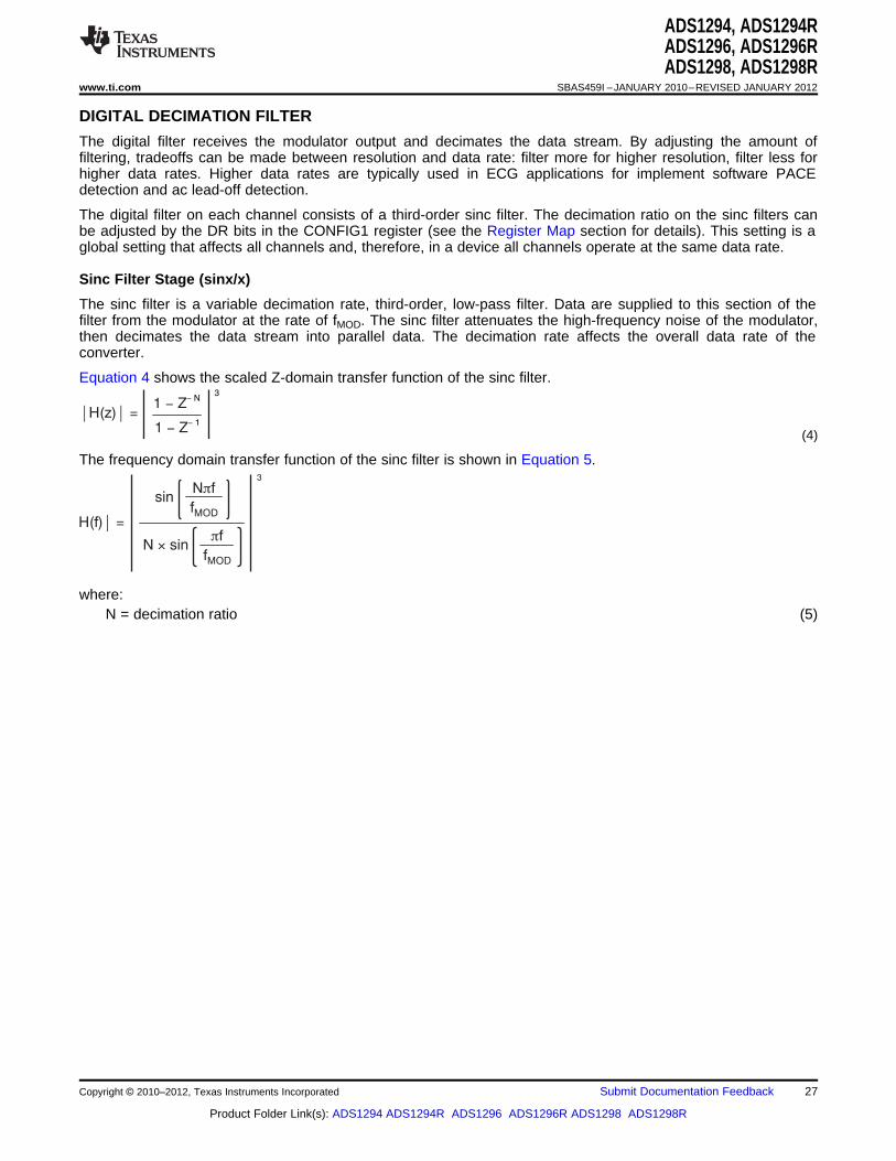
The sinc filter has notches (or zeroes) that occur at the output data rate and multiples thereof. At thesefrequencies, the filter has infinite attenuation. Figure 30 shows the frequency response of the sinc filter andFigure 31 shows the roll-off of the sinc filter. With a step change at input, the filter takes 3 × tDR to settle. After arising edge of the START signal, the filter takes tSETTLE time to give the first data output. The settling time of thefilters at various data rates are discussed in the START subsection of the SPI Interface section. Figure 32 andFigure 33 show the filter transfer function until fMOD/2 and fMOD/16, respectively, at different data rates. Figure 34shows the transfer function extended until 4 × fMOD. It can be seen that the passband of the ADS129x repeatsitself at every fMOD. The input R-C anti-aliasing filters in the system should be chosen such that any interferencein frequencies around multiples of fMOD are attenuated sufficiently.
Figure 30. Sinc Filter Frequency Response Figure 31. Sinc Filter Roll-Off
Figure 32. Transfer Function of On-Chip Figure 33. Transfer Function of On-ChipDecimation Filters Until fMOD/2 Decimation Filters Until fMOD/16
Figure 34. Transfer Function of On-Chip Decimation FiltersUntil 4fMOD for DR[2:0] = 000 and DR[2:0] = 110
28 Submit Documentation Feedback Copyright © 2010–2012, Texas Instruments Incorporated
Product Folder Link(s): ADS1294 ADS1294R ADS1296 ADS1296R ADS1298 ADS1298R
22 Fm
To ADC Reference Inputs
VCAP1
10 Fm
VREFP
VREFN
Bandgap2.4V or 4V
AVSS
R1(1)
R3(1)
R2(1)
100W
100kW
100W
OPA211
10pF
0.1 Fm
+5V
0.1 Fm10 Fm
100 Fm22 Fm
OUTVIN+5V
TRIM22 Fm
REF5025
To VREFP Pin
ADS1294, ADS1294RADS1296, ADS1296RADS1298, ADS1298R
www.ti.com SBAS459I –JANUARY 2010–REVISED JANUARY 2012
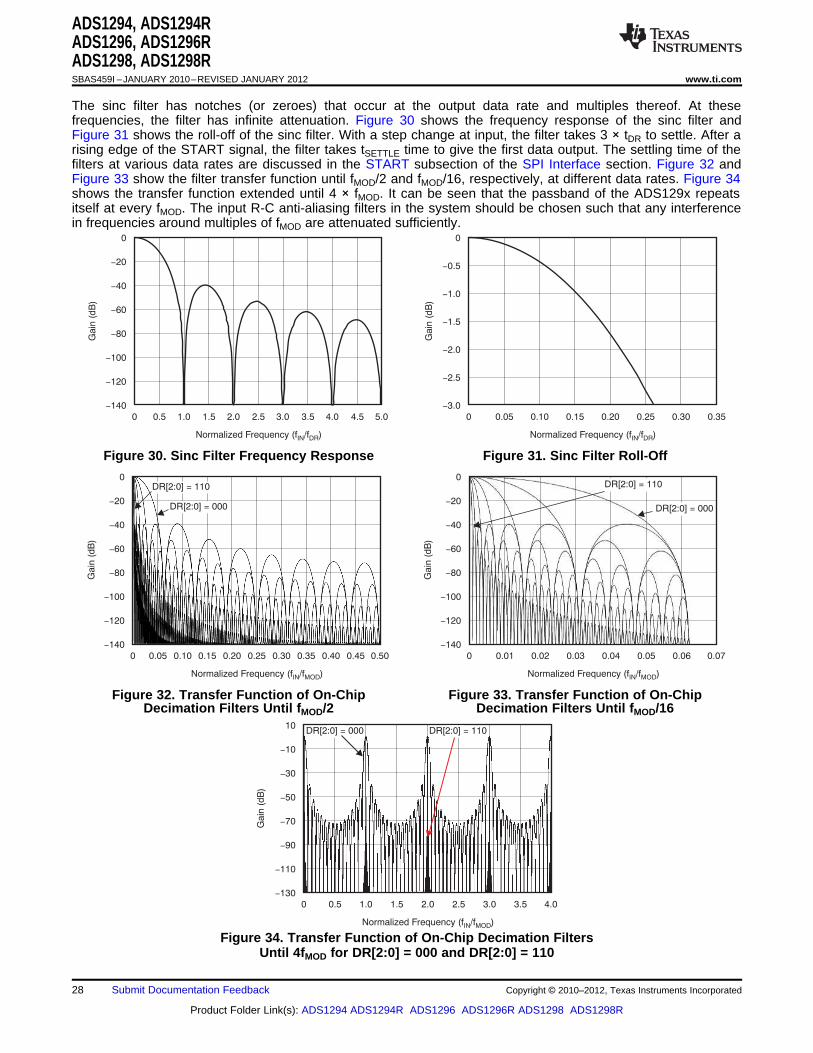
REFERENCE
Figure 35 shows a simplified block diagram of the internal reference of the ADS129x. The reference voltage isgenerated with respect to AVSS. When using the internal voltage reference, connect VREFN to AVSS.
(1) For VREF = 2.4V: R1 = 12.5kΩ, R2 = 25kΩ, and R3 = 25kΩ. For VREF = 4V: R1 = 10.5kΩ, R2 = 15kΩ, and R3 = 35kΩ.
Figure 35. Internal Reference
The external band-limiting capacitors determine the amount of reference noise contribution. For high-end ECGsystems, the capacitor values should be chosen such that the bandwidth is limited to less than 10Hz, so that thereference noise does not dominate the system noise. When using a 3V analog supply, the internal referencemust be set to 2.4V. In case of a 5V analog supply, the internal reference can be set to 4V by setting theVREF_4V bit in the CONFIG2 register.
Alternatively, the internal reference buffer can be powered down and VREFP can be applied externally. Figure 36shows a typical external reference drive circuitry. Power-down is controlled by the PD_REFBUF bit in theCONFIG3 register. By default the device wakes up in external reference mode.
Figure 36. External Reference Driver
Copyright © 2010–2012, Texas Instruments Incorporated Submit Documentation Feedback 29
Product Folder Link(s): ADS1294 ADS1294R ADS1296 ADS1296R ADS1298 ADS1298R
ADS1294, ADS1294RADS1296, ADS1296RADS1298, ADS1298RSBAS459I –JANUARY 2010–REVISED JANUARY 2012 www.ti.com
CLOCK
The ADS129x provide two different methods for device clocking: internal and external. Internal clocking is ideallysuited for low-power, battery-powered systems. The internal oscillator is trimmed for accuracy at roomtemperature. Over the specified temperature range the accuracy varies; see the Electrical Characteristics. Clockselection is controlled by the CLKSEL pin and the CLK_EN register bit.
The CLKSEL pin selects either the internal or external clock. The CLK_EN bit in the CONFIG1 register enablesand disables the oscillator clock to be output in the CLK pin. A truth table for these two pins is shown in Table 7.The CLK_EN bit is useful when multiple devices are used in a daisy-chain configuration. It is recommended thatduring power-down the external clock be shut down to save power.
Table 7. CLKSEL Pin and CLK_EN Bit
CONFIG1.CLK_ENCLKSEL PIN BIT CLOCK SOURCE CLK PIN STATUS
0 X External clock Input: external clock
1 0 Internal clock oscillator 3-state
1 1 Internal clock oscillator Output: internal clock oscillator
DATA FORMAT
The ADS129x output 24 bits of data per channel in binary twos complement format, MSB first. The LSB has aweight of VREF/(223 – 1). A positive full-scale input produces an output code of 7FFFFFh and the negativefull-scale input produces an output code of 800000h. The output clips at these codes for signals exceedingfull-scale. Table 8 summarizes the ideal output codes for different input signals. Note that for DR[2:0] = 000 and001, the device has only 17 and 19 bits of resolution, respectively. The last seven (in 17-bit mode) or five (in19-bit mode) bits can be ignored.
Table 8. Ideal Output Code versus Input Signal (1) (2)
INPUT SIGNAL, VIN(AINP – AINN) IDEAL OUTPUT CODE (3)
≥ VREF 7FFFFFh
+VREF/(223 – 1) 000001h
0 000000h
–VREF/(223 – 1) FFFFFFh
≤ –VREF (223/223 – 1) 800000h
(1) Only valid for 24-bit resolution data rates.(2) Assumes gain = 1.(3) Excludes effects of noise, linearity, offset, and gain error.
30 Submit Documentation Feedback Copyright © 2010–2012, Texas Instruments Incorporated
Product Folder Link(s): ADS1294 ADS1294R ADS1296 ADS1296R ADS1298 ADS1298R
ADS1294, ADS1294RADS1296, ADS1296RADS1298, ADS1298R
www.ti.com SBAS459I –JANUARY 2010–REVISED JANUARY 2012
SPI INTERFACE
The SPI-compatible serial interface consists of four signals: CS, SCLK, DIN, and DOUT. The interface readsconversion data, reads and writes registers, and controls the ADS129x operation. The DRDY output is used as astatus signal to indicate when data are ready. DRDY goes low when new data are available.
Chip Select (CS)
Chip select (CS) selects the ADS129x devices for SPI communication. While CS is low the serial interface isactive CS must remain low for the entire duration of the serial communication. After the serial communication isfinished, always wait four or more tCLK cycles before taking CS high. When CS is taken high, the serial interfaceis reset, SCLK and DIN are ignored, and DOUT enters a high-impedance state. DRDY asserts when dataconversion is complete, regardless of whether CS is high or low.
While ADS129x is selected the device will attempt to decode and execute commands every eight serial clocks. Ifthe devices ceases to execute serial commands, it is possible extra clock pulses were presented and placed theserial interface in an unknown state. Take CS high and back low to reset the serial interface to a known state.
Serial Clock (SCLK)
SCLK is the serial peripheral interface (SPI) serial clock. It is used to shift in commands and shift out data fromthe device. The serial clock (SCLK) features a Schmitt-triggered input and clocks data on the DIN and DOUTpins into and out of the ADS129x. Even though the input has hysteresis, it is recommended to keep SCLK asclean as possible to prevent glitches from accidentally forcing a clock event. The absolute maximum limit forSCLK is specified in the Serial Interface Timing table.
While ADS129x is selected(CS = LOW), the device attempts to decode and execute commands every eightserial clocks. It is therefore recommended that multiples of 8 SCLKs be presented every serial transfer to keepthe interface in a normal operating mode. If the interface ceases to function because of extra serial clocks, it canbe reset by toggling CS high and back to low.
For a single device, the minimum speed needed for the SCLK depends on the number of channels, number ofbits of resolution, and output data rate. (For multiple cascaded devices, see the Cascade Mode subsection of theMultiple Device Configuration section.)tSCLK < (tDR – 4tCLK)/(NBITS × NCHANNELS + 24) (6)
For example, if the ADS1298 is used in a 500SPS mode (eight channels, 24-bit resolution), the minimum SCLKspeed is 110kHz.
Data retrieval can be done either by putting the device in RDATAC mode or by issuing a RDATA command fordata on demand. The above SCLK rate limitation applies to RDATAC. For the RDATA command, the limitationapplies if data must be read between two consecutive DRDY signals. The above calculation assumes that thereare no other commands issued between data captures.
Data Input (DIN)
The data input pin (DIN) is used along with SCLK to communicate with the ADS129x (opcode commands andregister data). The device latches data on DIN on the falling edge of SCLK.
Copyright © 2010–2012, Texas Instruments Incorporated Submit Documentation Feedback 31
Product Folder Link(s): ADS1294 ADS1294R ADS1296 ADS1296R ADS1298 ADS1298R
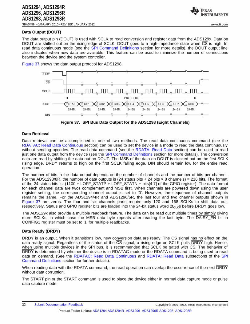
CS
SCLK
DRDY
DOUT STAT
24-Bit 24-Bit 24-Bit 24-Bit 24-Bit 24-Bit 24-Bit 24-Bit 24-Bit
CH1 CH2 CH3 CH4 CH5 CH6 CH7 CH8
216 SCLKs
DIN
ADS1294, ADS1294RADS1296, ADS1296RADS1298, ADS1298RSBAS459I –JANUARY 2010–REVISED JANUARY 2012 www.ti.com
Data Output (DOUT)
The data output pin (DOUT) is used with SCLK to read conversion and register data from the ADS129x. Data onDOUT are shifted out on the rising edge of SCLK. DOUT goes to a high-impedance state when CS is high. Inread data continuous mode (see the SPI Command Definitions section for more details), the DOUT output linealso indicates when new data are available. This feature can be used to minimize the number of connectionsbetween the device and the system controller.
Figure 37 shows the data output protocol for ADS1298.
Figure 37. SPI Bus Data Output for the ADS1298 (Eight Channels)
Data Retrieval
Data retrieval can be accomplished in one of two methods. The read data continuous command (see theRDATAC: Read Data Continuous section) can be used to set the device in a mode to read the data continuouslywithout sending opcodes. The read data command (see the RDATA: Read Data section) can be used to readjust one data output from the device (see the SPI Command Definitions section for more details). The conversiondata are read by shifting the data out on DOUT. The MSB of the data on DOUT is clocked out on the first SCLKrising edge. DRDY returns to high on the first SCLK falling edge. DIN should remain low for the entire readoperation.
The number of bits in the data output depends on the number of channels and the number of bits per channel.For the ADS1298/8R, the number of data outputs is (24 status bits + 24 bits × 8 channels) = 216 bits. The formatof the 24 status bits is: (1100 + LOFF_STATP + LOFF_STATN + bits[4:7] of the GPIO register). The data formatfor each channel data are twos complement and MSB first. When channels are powered down using the userregister setting, the corresponding channel output is set to '0'. However, the sequence of channel outputsremains the same. For the ADS1294/4R and ADS1296/6R, the last four and two channel outputs shown inFigure 37 are zeros. The four and six channels parts require only 120 and 168 SCLKs to shift data out,respectively. Status and GPIO register bits are loaded into the 24-bit status word 2tCLKs before DRDY goes low.
The ADS129x also provide a multiple readback feature. The data can be read out multiple times by simply givingmore SCLKs, in which case the MSB data byte repeats after reading the last byte. The DAISY_EN bit inCONFIG1 register must be set to '1' for multiple readbacks.
Data Ready (DRDY)
DRDY is an output. When it transitions low, new conversion data are ready. The CS signal has no effect on thedata ready signal. Regardless of the status of the CS signal, a rising edge on SCLK pulls DRDY high. Hence,when using multiple devices in the SPI bus, it is recommended that SCLK be gated with CS. The behavior ofDRDY is determined by whether the device is in RDATAC mode or the RDATA command is being used to readdata on demand. (See the RDATAC: Read Data Continuous and RDATA: Read Data subsections of the SPICommand Definitions section for further details).
When reading data with the RDATA command, the read operation can overlap the occurrence of the next DRDYwithout data corruption.
The START pin or the START command is used to place the device either in normal data capture mode or pulsedata capture mode.
32 Submit Documentation Feedback Copyright © 2010–2012, Texas Instruments Incorporated
Product Folder Link(s): ADS1294 ADS1294R ADS1296 ADS1296R ADS1298 ADS1298R
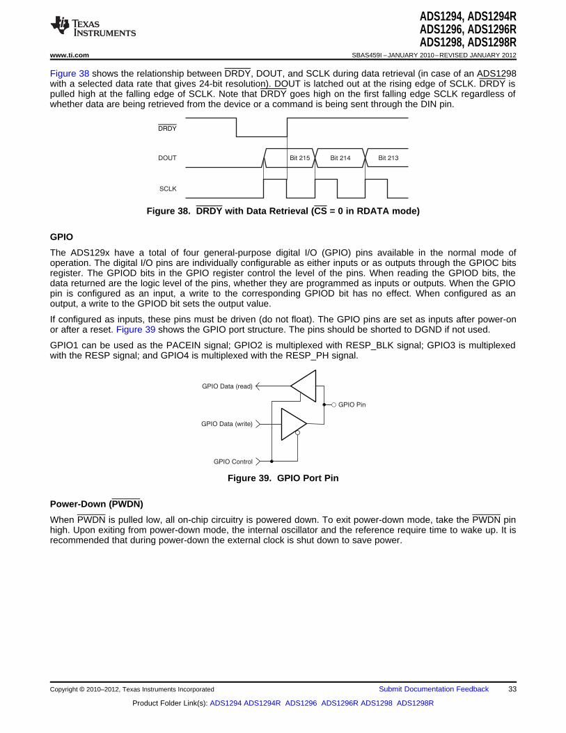
DRDY
DOUT
SCLK
Bit 215 Bit 214 Bit 213
GPIO Pin
GPIO Data (read)
GPIO Data (write)
GPIO Control
ADS1294, ADS1294RADS1296, ADS1296RADS1298, ADS1298R
www.ti.com SBAS459I –JANUARY 2010–REVISED JANUARY 2012
Figure 38 shows the relationship between DRDY, DOUT, and SCLK during data retrieval (in case of an ADS1298with a selected data rate that gives 24-bit resolution). DOUT is latched out at the rising edge of SCLK. DRDY ispulled high at the falling edge of SCLK. Note that DRDY goes high on the first falling edge SCLK regardless ofwhether data are being retrieved from the device or a command is being sent through the DIN pin.
Figure 38. DRDY with Data Retrieval (CS = 0 in RDATA mode)
GPIO
The ADS129x have a total of four general-purpose digital I/O (GPIO) pins available in the normal mode ofoperation. The digital I/O pins are individually configurable as either inputs or as outputs through the GPIOC bitsregister. The GPIOD bits in the GPIO register control the level of the pins. When reading the GPIOD bits, thedata returned are the logic level of the pins, whether they are programmed as inputs or outputs. When the GPIOpin is configured as an input, a write to the corresponding GPIOD bit has no effect. When configured as anoutput, a write to the GPIOD bit sets the output value.
If configured as inputs, these pins must be driven (do not float). The GPIO pins are set as inputs after power-onor after a reset. Figure 39 shows the GPIO port structure. The pins should be shorted to DGND if not used.
GPIO1 can be used as the PACEIN signal; GPIO2 is multiplexed with RESP_BLK signal; GPIO3 is multiplexedwith the RESP signal; and GPIO4 is multiplexed with the RESP_PH signal.
Figure 39. GPIO Port Pin
Power-Down (PWDN)
When PWDN is pulled low, all on-chip circuitry is powered down. To exit power-down mode, take the PWDN pinhigh. Upon exiting from power-down mode, the internal oscillator and the reference require time to wake up. It isrecommended that during power-down the external clock is shut down to save power.
Copyright © 2010–2012, Texas Instruments Incorporated Submit Documentation Feedback 33
Product Folder Link(s): ADS1294 ADS1294R ADS1296 ADS1296R ADS1298 ADS1298R
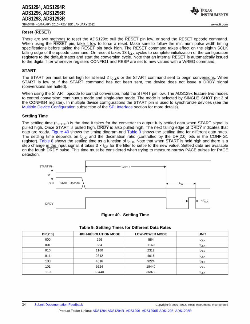
STAR coT Op de
START Pin
D NI
4/fCLKDRDY
or
tDR
tSETTLE
ADS1294, ADS1294RADS1296, ADS1296RADS1298, ADS1298RSBAS459I –JANUARY 2010–REVISED JANUARY 2012 www.ti.com
Reset (RESET)
There are two methods to reset the ADS129x: pull the RESET pin low, or send the RESET opcode command.When using the RESET pin, take it low to force a reset. Make sure to follow the minimum pulse width timingspecifications before taking the RESET pin back high. The RESET command takes effect on the eighth SCLKfalling edge of the opcode command. On reset it takes 18 tCLK cycles to complete initialization of the configurationregisters to the default states and start the conversion cycle. Note that an internal RESET is automatically issuedto the digital filter whenever registers CONFIG1 and RESP are set to new values with a WREG command.
START
The START pin must be set high for at least 2 tCLKs or the START command sent to begin conversions. WhenSTART is low or if the START command has not been sent, the device does not issue a DRDY signal(conversions are halted).
When using the START opcode to control conversion, hold the START pin low. The ADS129x feature two modesto control conversion: continuous mode and single-shot mode. The mode is selected by SINGLE_SHOT (bit 3 ofthe CONFIG4 register). In multiple device configurations the START pin is used to synchronize devices (see theMultiple Device Configuration subsection of the SPI Interface section for more details).
Settling Time
The settling time (tSETTLE) is the time it takes for the converter to output fully settled data when START signal ispulled high. Once START is pulled high, DRDY is also pulled high. The next falling edge of DRDY indicates thatdata are ready. Figure 40 shows the timing diagram and Table 9 shows the settling time for different data rates.The settling time depends on fCLK and the decimation ratio (controlled by the DR[2:0] bits in the CONFIG1register). Table 8 shows the settling time as a function of tCLK. Note that when START is held high and there is astep change in the input signal, it takes 3 × tDR for the filter to settle to the new value. Settled data are availableon the fourth DRDY pulse. This time must be considered when trying to measure narrow PACE pulses for PACEdetection.
Figure 40. Settling Time
Table 9. Settling Times for Different Data Rates
DR[2:0] HIGH-RESOLUTION MODE LOW-POWER MODE UNIT
000 296 584 tCLK
001 584 1160 tCLK
010 1160 2312 tCLK
011 2312 4616 tCLK
100 4616 9224 tCLK
101 9224 18440 tCLK
110 18440 36872 tCLK
34 Submit Documentation Feedback Copyright © 2010–2012, Texas Instruments Incorporated
Product Folder Link(s): ADS1294 ADS1294R ADS1296 ADS1296R ADS1298 ADS1298R

START
Opcode
(1)
S RT PinTA
DIN
tDR
tSETTLEDRDY
STOP
Opcode
(1)
or or
tSDSU
tDSHD
STOP Opcode
DRDY and DOUT
START Pin
or
STOP(1)STOP(1)
ADS1294, ADS1294RADS1296, ADS1296RADS1298, ADS1298R
www.ti.com SBAS459I –JANUARY 2010–REVISED JANUARY 2012
Continuous Mode
Conversions begin when the START pin is taken high for at least 2 tCLKs or when the START opcode commandis sent. As seen in Figure 41, the DRDY output goes high when conversions are started and goes low when dataare ready. Conversions continue indefinitely until the START pin is taken low or the STOP opcode command istransmitted. When the START pin is pulled low or the stop command is issued, the conversion in progress isallowed to complete. Figure 42 and Table 10 show the required timing of DRDY to the START pin and theSTART/STOP opcode commands when controlling conversions in this mode. To keep the converter runningcontinuously, the START pin can be permanently tied high. Note that when switching from pulse mode tocontinuous mode, the START signal is pulsed or a STOP command must be issued followed by a STARTcommand. This conversion mode is ideal for applications that require a fixed-continuous stream of conversionsresults.
(1) START and STOP opcode commands take effect on the seventh SCLK falling edge.
Figure 41. Continuous Conversion Mode
(1) START and STOP commands take effect on the seventh SCLK falling edge at the end of the opcode transmission.
Figure 42. START to DRDY Timing
Table 10. Timing Characteristics for Figure 42(1)
SYMBOL DESCRIPTION MIN UNIT
START pin low or STOP opcode to DRDY setup timetSDSU 16 tCLKto halt further conversions
START pin low or STOP opcode to complete currenttDSHD 16 tCLKconversion
(1) START and STOP commands take effect on the seventh SCLK falling edge at the end of the opcode transmission.
Copyright © 2010–2012, Texas Instruments Incorporated Submit Documentation Feedback 35
Product Folder Link(s): ADS1294 ADS1294R ADS1296 ADS1296R ADS1298 ADS1298R
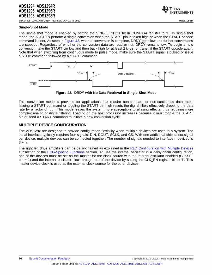
START
DRDY
4 f/ CLK 4 f/ CLKData Updating
tSETTLE
ADS1294, ADS1294RADS1296, ADS1296RADS1298, ADS1298RSBAS459I –JANUARY 2010–REVISED JANUARY 2012 www.ti.com
Single-Shot Mode
The single-shot mode is enabled by setting the SINGLE_SHOT bit in CONFIG4 register to '1'. In single-shotmode, the ADS129x perform a single conversion when the START pin is taken high or when the START opcodecommand is sent. As seen in Figure 42, when a conversion is complete, DRDY goes low and further conversionsare stopped. Regardless of whether the conversion data are read or not, DRDY remains low. To begin a newconversion, take the START pin low and then back high for at least 2 tCLKs, or transmit the START opcode again.Note that when switching from continuous mode to pulse mode, make sure the START signal is pulsed or issuea STOP command followed by a START command.
Figure 43. DRDY with No Data Retrieval in Single-Shot Mode
This conversion mode is provided for applications that require non-standard or non-continuous data rates.Issuing a START command or toggling the START pin high resets the digital filter, effectively dropping the datarate by a factor of four. This mode leaves the system more susceptible to aliasing effects, thus requiring morecomplex analog or digital filtering. Loading on the host processor increases because it must toggle the STARTpin or send a START command to initiate a new conversion cycle.
MULTIPLE DEVICE CONFIGURATION
The ADS129x are designed to provide configuration flexibility when multiple devices are used in a system. Theserial interface typically requires four signals: DIN, DOUT, SCLK, and CS. With one additional chip select signalper device, multiple devices can be connected together. The number of signals needed to interface n devices is3 + n.
The right leg drive amplifiers can be daisy-chained as explained in the RLD Configuration with Multiple Devicessubsection of the ECG-Specific Functions section. To use the internal oscillator in a daisy-chain configuration,one of the devices must be set as the master for the clock source with the internal oscillator enabled (CLKSELpin = 1) and the internal oscillator clock brought out of the device by setting the CLK_EN register bit to '1'. Thismaster device clock is used as the external clock source for the other devices.
36 Submit Documentation Feedback Copyright © 2010–2012, Texas Instruments Incorporated
Product Folder Link(s): ADS1294 ADS1294R ADS1296 ADS1296R ADS1298 ADS1298R
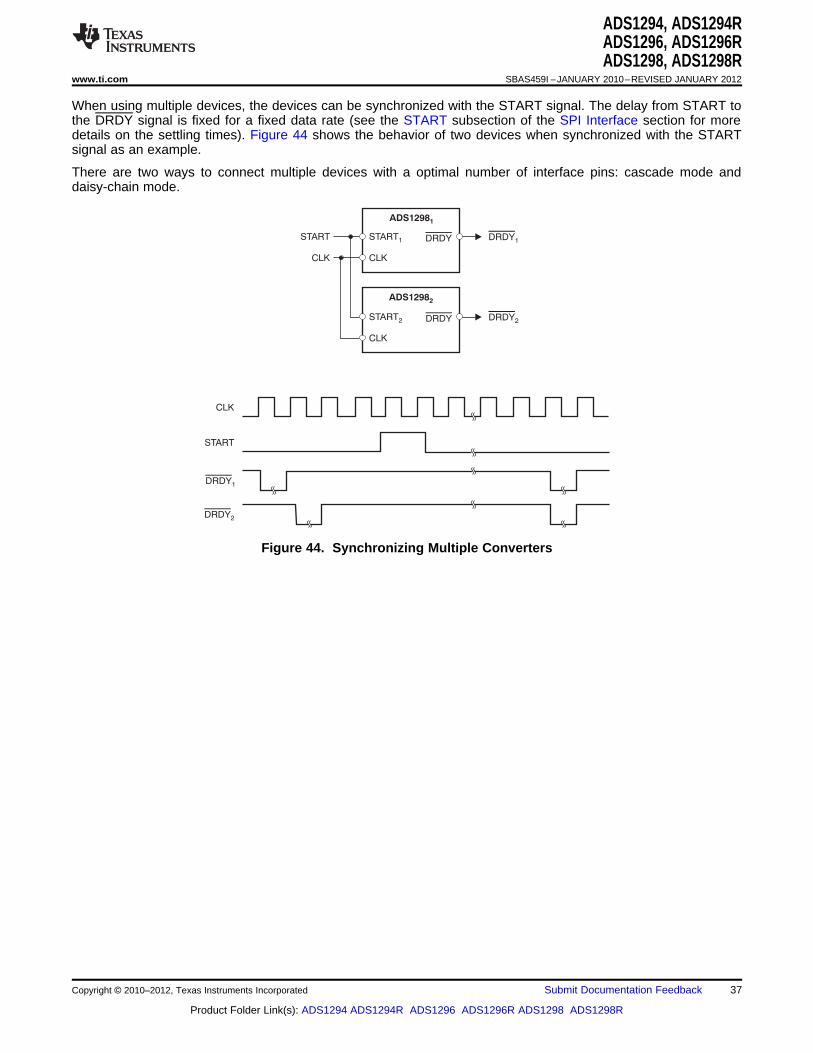
START1
ADS12981
CLK
DRDY DRDY1
START
CLK
START2
ADS12982
CLK
DRDY DRDY2
START
CLK
DRDY1
DRDY2
ADS1294, ADS1294RADS1296, ADS1296RADS1298, ADS1298R
www.ti.com SBAS459I –JANUARY 2010–REVISED JANUARY 2012
When using multiple devices, the devices can be synchronized with the START signal. The delay from START tothe DRDY signal is fixed for a fixed data rate (see the START subsection of the SPI Interface section for moredetails on the settling times). Figure 44 shows the behavior of two devices when synchronized with the STARTsignal as an example.
There are two ways to connect multiple devices with a optimal number of interface pins: cascade mode anddaisy-chain mode.
Figure 44. Synchronizing Multiple Converters
Copyright © 2010–2012, Texas Instruments Incorporated Submit Documentation Feedback 37
Product Folder Link(s): ADS1294 ADS1294R ADS1296 ADS1296R ADS1298 ADS1298R
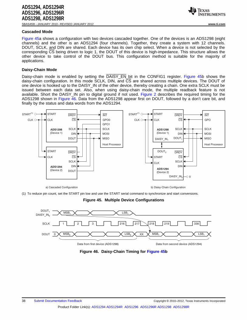
START DRDY
CS
SCLK
DIN
DOUT
ADS1298
(Device 1)
START DRDY
CS
SCLK
DIN
DOUT
ADS1294
(Device 2)
START(1)
a) Cascaded Configuration
CLK
CLK
INT
GPO0
GPO1
SCLK
MOSI
Host Processor
MISO
CLK
START DRDY
CS
SCLK
DIN
DOUT1
ADS1298
(Device 1)
START
DRDY
CS
SCLK
DIN
DAISY_IN2
ADS1294
(Device 2)
START(1)
b) Daisy-Chain Configuration
CLK
CLK
INT
GPO
SCLK
MOSI
Host Processor
MISO
CLK
0
DOUT2
DAISY_IN1
DOUT
DAISY_IN1
0
DO TU 0
SCLK
MSB1
MSB0
21 3 216 217 218
MSB1LSB0
LSB1
219 338
LSB1
Da a ft rom first d ce (evi ADS1298) Da a ft rom second vide ce (ADS1294)
XX
ADS1294, ADS1294RADS1296, ADS1296RADS1298, ADS1298RSBAS459I –JANUARY 2010–REVISED JANUARY 2012 www.ti.com
Cascaded Mode
Figure 45a shows a configuration with two devices cascaded together. One of the devices is an ADS1298 (eightchannels) and the other is an ADS1294 (four channels). Together, they create a system with 12 channels.DOUT, SCLK, and DIN are shared. Each device has its own chip select. When a device is not selected by thecorresponding CS being driven to logic 1, the DOUT of this device is high-impedance. This structure allows theother device to take control of the DOUT bus. This configuration method is suitable for the majority ofapplications.
Daisy-Chain Mode
Daisy-chain mode is enabled by setting the DAISY_EN bit in the CONFIG1 register. Figure 45b shows thedaisy-chain configuration. In this mode SCLK, DIN, and CS are shared across multiple devices. The DOUT ofone device is hooked up to the DAISY_IN of the other device, thereby creating a chain. One extra SCLK must beissued between each data set. Also, when using daisy-chain mode, the multiple readback feature is notavailable. Short the DAISY_IN pin to digital ground if not used. Figure 2 describes the required timing for theADS1298 shown in Figure 46. Data from the ADS1298 appear first on DOUT, followed by a don’t care bit, andfinally by the status and data words from the ADS1294.
(1) To reduce pin count, set the START pin low and use the START serial command to synchronize and start conversions.
Figure 45. Multiple Device Configurations
Figure 46. Daisy-Chain Timing for Figure 45b
38 Submit Documentation Feedback Copyright © 2010–2012, Texas Instruments Incorporated
Product Folder Link(s): ADS1294 ADS1294R ADS1296 ADS1296R ADS1298 ADS1298R

fSCLK
f (N )(NDR BITS CHANNELS) + 24N =DEVICES
ADS1294, ADS1294RADS1296, ADS1296RADS1298, ADS1298R
www.ti.com SBAS459I –JANUARY 2010–REVISED JANUARY 2012
In a case where all devices in the chain operate in the same register setting, DIN can be shared as well andthereby reduce the SPI communication signals to four, regardless of the number of devices. However, becausethe individual devices cannot be programmed, the RLD driver cannot be shared among the multiple devices.Furthermore, an external clock must be used.
Note that from Figure 2, the SCLK rising edge shifts data out of the ADS129x on DOUT. The SCLK rising edge isalso used to latch data into the device DAISY_IN pin down the chain. This architecture allows for a faster SCLKrate speed, but it also makes the interface sensitive to board level signal delays. The more devices in the chain,the more challenging it could become to adhere to setup and hold times. A star pattern connection of SCLK to alldevices, minimizing length of DOUT, and other PCB layout techniques help. Placing delay circuits such asbuffers between DOUT and DAISY_IN are ways to mitigate this challenge. One other option is to insert a Dflip-flop between DOUT and DAISY_IN clocked on an inverted SCLK. Note also that daisy-chain mode requiressome software overhead to recombine data bits spread across byte boundaries.
The maximum number of devices that can be daisy-chained depends on the data rate at which the device isbeing operated. The maximum number of devices can be estimated with Equation 7.
where:NBITS = device resolution (depends on data rate), andNCHANNELS = number of channels in the device (4, 6, or 8). (7)
For example, when the ADS1298 (eight-channel, 24-bit version) is operated at a 2kSPS data rate with a 4MHzfSCLK, 10 devices can be daisy-chained.
Copyright © 2010–2012, Texas Instruments Incorporated Submit Documentation Feedback 39
Product Folder Link(s): ADS1294 ADS1294R ADS1296 ADS1296R ADS1298 ADS1298R
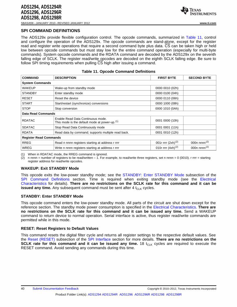
ADS1294, ADS1294RADS1296, ADS1296RADS1298, ADS1298RSBAS459I –JANUARY 2010–REVISED JANUARY 2012 www.ti.com
SPI COMMAND DEFINITIONS
The ADS129x provide flexible configuration control. The opcode commands, summarized in Table 11, controland configure the operation of the ADS129x. The opcode commands are stand-alone, except for the registerread and register write operations that require a second command byte plus data. CS can be taken high or heldlow between opcode commands but must stay low for the entire command operation (especially for multi-bytecommands). System opcode commands and the RDATA command are decoded by the ADS129x on the seventhfalling edge of SCLK. The register read/write opcodes are decoded on the eighth SCLK falling edge. Be sure tofollow SPI timing requirements when pulling CS high after issuing a command.
Table 11. Opcode Command Definitions
COMMAND DESCRIPTION FIRST BYTE SECOND BYTE
System Commands
WAKEUP Wake-up from standby mode 0000 0010 (02h)
STANDBY Enter standby mode 0000 0100 (04h)
RESET Reset the device 0000 0110 (06h)
START Start/restart (synchronize) conversions 0000 1000 (08h)
STOP Stop conversion 0000 1010 (0Ah)
Data Read Commands
Enable Read Data Continuous mode.RDATAC 0001 0000 (10h)This mode is the default mode at power-up. (1)
SDATAC Stop Read Data Continuously mode 0001 0001 (11h)
RDATA Read data by command; supports multiple read back. 0001 0010 (12h)
Register Read Commands
RREG Read n nnnn registers starting at address r rrrr 001r rrrr (2xh) (2) 000n nnnn (2)
WREG Write n nnnn registers starting at address r rrrr 010r rrrr (4xh) (2) 000n nnnn (2)
(1) When in RDATAC mode, the RREG command is ignored.(2) n nnnn = number of registers to be read/written – 1. For example, to read/write three registers, set n nnnn = 0 (0010). r rrrr = starting
register address for read/write opcodes.
WAKEUP: Exit STANDBY Mode
This opcode exits the low-power standby mode; see the STANDBY: Enter STANDBY Mode subsection of theSPI Command Definitions section. Time is required when exiting standby mode (see the ElectricalCharacteristics for details). There are no restrictions on the SCLK rate for this command and it can beissued any time. Any subsequent command must be sent after 4 tCLK cycles.
STANDBY: Enter STANDBY Mode
This opcode command enters the low-power standby mode. All parts of the circuit are shut down except for thereference section. The standby mode power consumption is specified in the Electrical Characteristics. There areno restrictions on the SCLK rate for this command and it can be issued any time. Send a WAKEUPcommand to return device to normal operation. Serial interface is active, thus register read/write commands arepermitted while in this mode.
RESET: Reset Registers to Default Values
This command resets the digital filter cycle and returns all register settings to the respective default values. Seethe Reset (RESET) subsection of the SPI Interface section for more details. There are no restrictions on theSCLK rate for this command and it can be issued any time. 18 tCLK cycles are required to execute theRESET command. Avoid sending any commands during this time.
40 Submit Documentation Feedback Copyright © 2010–2012, Texas Instruments Incorporated
Product Folder Link(s): ADS1294 ADS1294R ADS1296 ADS1296R ADS1298 ADS1298R

START
DRDY
CS
SCLK
DINtUPDATE
DOUTHi-Z
RDATAC Opcode
Status Register + 8-Channel Data (216 Bits) Next Data
ADS1294, ADS1294RADS1296, ADS1296RADS1298, ADS1298R
www.ti.com SBAS459I –JANUARY 2010–REVISED JANUARY 2012
START: Start Conversions
This opcode starts data conversions. Tie the START pin low to control conversions by command. If conversionsare in progress this command has no effect. The STOP opcode command is used to stop conversions. If theSTART command is immediately followed by a STOP command, there must be a gap of 4 tCLK cycles betweenthe two commands. When the START opcode is sent to the device, keep the START pin low until the STOPcommand is issued. (See the START subsection of the SPI Interface section for more details.) There are norestrictions on the SCLK rate for this command and it can be issued any time.
STOP: Stop Conversions
This opcode stops conversions. Tie the START pin low to control conversions by command. When the STOPcommand is sent, the conversion in progress completes and further conversions are stopped. If conversions arealready stopped, this command has no effect. There are no restrictions on the SCLK rate for this commandand it can be issued any time.
RDATAC: Read Data Continuous
This opcode enables the output of conversion data on each DRDY without the need to issue subsequent readdata opcodes. This mode places the conversion data in the output register and may be shifted out directly. Theread data continuous mode is the default mode of the device and the device defaults to this mode on power-upand reset.
RDATAC mode is cancelled by the Stop Read Data Continuous command. If the device is in RDATAC mode, aSDATAC command must be issued before any other commands can be sent to the device. There is norestriction on the SCLK rate for this command. However, the subsequent data retrieval SCLKs or the SDATACopcode command should wait at least 4 tCLK cycles. The timing for RDATAC is shown in Figure 47. As Figure 47shows, there is a keep out zone of 4 tCLK cycles around the DRDY pulse when this command cannot be issued.If no data are retrieved from the device, DOUT and DRDY behave similarly in this mode. To retrieve data fromthe device after RDATAC command is issued, make sure either the START pin is high or the START commandis issued. Figure 47 shows the recommended way to use the RDATAC command. RDATAC is ideally suited forapplications such as data loggers or recorders where registers are set once and do not need to be re-configured.
(1) tUPDATE = 4/fCLK. Do not read data during this time.
Figure 47. RDATAC Usage
SDATAC: Stop Read Data Continuous
This opcode cancels the Read Data Continuous mode. There is no restriction on the SCLK rate for thiscommand, but the subsequent command must wait for 4 tCLK cycles.
Copyright © 2010–2012, Texas Instruments Incorporated Submit Documentation Feedback 41
Product Folder Link(s): ADS1294 ADS1294R ADS1296 ADS1296R ADS1298 ADS1298R
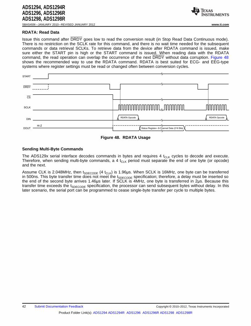
Hi-Z
START
DRDY
CS
SCLK
DIN
DOUT
RDATA Opcode
Status Register+ 8-Channel Data (216 Bits)
RDATA Opcode
ADS1294, ADS1294RADS1296, ADS1296RADS1298, ADS1298RSBAS459I –JANUARY 2010–REVISED JANUARY 2012 www.ti.com
RDATA: Read Data
Issue this command after DRDY goes low to read the conversion result (in Stop Read Data Continuous mode).There is no restriction on the SCLK rate for this command, and there is no wait time needed for the subsequentcommands or data retrieval SCLKs. To retrieve data from the device after RDATA command is issued, makesure either the START pin is high or the START command is issued. When reading data with the RDATAcommand, the read operation can overlap the occurrence of the next DRDY without data corruption. Figure 48shows the recommended way to use the RDATA command. RDATA is best suited for ECG- and EEG-typesystems where register settings must be read or changed often between conversion cycles.
Figure 48. RDATA Usage
Sending Multi-Byte Commands
The ADS129x serial interface decodes commands in bytes and requires 4 tCLK cycles to decode and execute.Therefore, when sending multi-byte commands, a 4 tCLK period must separate the end of one byte (or opcode)and the next.
Assume CLK is 2.048MHz, then tSDECODE (4 tCLK) is 1.96µs. When SCLK is 16MHz, one byte can be transferredin 500ns. This byte transfer time does not meet the tSDECODE specification; therefore, a delay must be inserted sothe end of the second byte arrives 1.46µs later. If SCLK is 4MHz, one byte is transferred in 2µs. Because thistransfer time exceeds the tSDECODE specification, the processor can send subsequent bytes without delay. In thislater scenario, the serial port can be programmed to cease single-byte transfer per cycle to multiple bytes.
42 Submit Documentation Feedback Copyright © 2010–2012, Texas Instruments Incorporated
Product Folder Link(s): ADS1294 ADS1294R ADS1296 ADS1296R ADS1298 ADS1298R
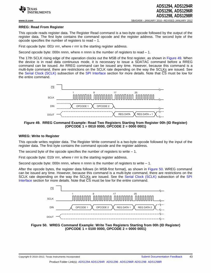
1 9 17 25
CS
SCLK
DIN OPCODE 1 OPCODE 2
DOUT REG DATA REG DATA + 1
1 9 17 25
CS
SCLK
DIN OPCODE 1 OPCODE 2 REG DATA 1 REG DATA 2
DOUT
ADS1294, ADS1294RADS1296, ADS1296RADS1298, ADS1298R
www.ti.com SBAS459I –JANUARY 2010–REVISED JANUARY 2012
RREG: Read From Register
This opcode reads register data. The Register Read command is a two-byte opcode followed by the output of theregister data. The first byte contains the command opcode and the register address. The second byte of theopcode specifies the number of registers to read – 1.
First opcode byte: 001r rrrr, where r rrrr is the starting register address.
Second opcode byte: 000n nnnn, where n nnnn is the number of registers to read – 1.
The 17th SCLK rising edge of the operation clocks out the MSB of the first register, as shown in Figure 49. Whenthe device is in read data continuous mode, it is necessary to issue a SDATAC command before a RREGcommand can be issued. An RREG command can be issued any time. However, because this command is amulti-byte command, there are restrictions on the SCLK rate depending on the way the SCLKs are issued. Seethe Serial Clock (SCLK) subsection of the SPI Interface section for more details. Note that CS must be low forthe entire command.
Figure 49. RREG Command Example: Read Two Registers Starting from Register 00h (ID Register)(OPCODE 1 = 0010 0000, OPCODE 2 = 0000 0001)
WREG: Write to Register
This opcode writes register data. The Register Write command is a two-byte opcode followed by the input of theregister data. The first byte contains the command opcode and the register address.
The second byte of the opcode specifies the number of registers to write – 1.
First opcode byte: 010r rrrr, where r rrrr is the starting register address.
Second opcode byte: 000n nnnn, where n nnnn is the number of registers to write – 1.
After the opcode bytes, the register data follows (in MSB-first format), as shown in Figure 50. WREG commandcan be issued any time. However, because this command is a multi-byte command, there are restrictions on theSCLK rate depending on the way the SCLKs are issued. See the Serial Clock (SCLK) subsection of the SPIInterface section for more details. Note that CS must be low for the entire command.
Figure 50. WREG Command Example: Write Two Registers Starting from 00h (ID Register)(OPCODE 1 = 0100 0000, OPCODE 2 = 0000 0001)
Copyright © 2010–2012, Texas Instruments Incorporated Submit Documentation Feedback 43
Product Folder Link(s): ADS1294 ADS1294R ADS1296 ADS1296R ADS1298 ADS1298R
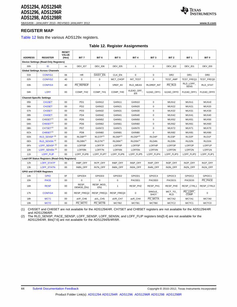
ADS1294, ADS1294RADS1296, ADS1296RADS1298, ADS1298RSBAS459I –JANUARY 2010–REVISED JANUARY 2012 www.ti.com
REGISTER MAP
Table 12 lists the various ADS129x registers.
Table 12. Register AssignmentsRESETVALUE
ADDRESS REGISTER (Hex) BIT 7 BIT 6 BIT 5 BIT 4 BIT 3 BIT 2 BIT 1 BIT 0
Device Settings (Read-Only Registers)
00h ID xx DEV_ID7 DEV_ID6 DEV_ID5 1 0 DEV_ID2 DEV_ID1 DEV_ID0
Global Settings Across Channels
01h CONFIG1 06 HR DAISY_EN CLK_EN 0 0 DR2 DR1 DR0
02h CONFIG2 40 0 0 WCT_CHOP INT_TEST 0 TEST_AMP TEST_FREQ1 TEST_FREQ0
RLD_LOFF_03h CONFIG3 40 PD_REFBUF 1 VREF_4V RLD_MEAS RLDREF_INT PD_RLD RLD_STAT
SENS
VLEAD_OFF_04h LOFF 00 COMP_TH2 COMP_TH1 COMP_TH0 ILEAD_OFF1 ILEAD_OFF0 FLEAD_OFF1 FLEAD_OFF0
EN
Channel-Specific Settings
05h CH1SET 00 PD1 GAIN12 GAIN11 GAIN10 0 MUXn2 MUXn1 MUXn0
06h CH2SET 00 PD2 GAIN22 GAIN21 GAIN20 0 MUX22 MUX21 MUX20
07h CH3SET 00 PD3 GAIN32 GAIN31 GAIN30 0 MUX32 MUX31 MUX30
08h CH4SET 00 PD4 GAIN42 GAIN41 GAIN40 0 MUX42 MUX41 MUX40
09h CH5SET(1) 00 PD5 GAIN52 GAIN51 GAIN50 0 MUX52 MUX51 MUX50
0Ah CH6SET(1) 00 PD6 GAIN62 GAIN61 GAIN60 0 MUX62 MUX61 MUX60
0Bh CH7SET(1) 00 PD7 GAIN72 GAIN71 GAIN70 0 MUX72 MUX71 MUX70
0Ch CH8SET(1) 00 PD8 GAIN82 GAIN81 GAIN80 0 MUX82 MUX81 MUX80
0Dh RLD_SENSP (2) 00 RLD8P(1) RLD7P(1) RLD6P(1) RLD5P(1) RLD4P RLD3P RLD2P RLD1P
0Eh RLD_SENSN (2) 00 RLD8N(1) RLD7N(1) RLD6N(1) RLD5N(1) RLD4N RLD3N RLD2N RLD1N
0Fh LOFF_SENSP (2) 00 LOFF8P LOFF7P LOFF6P LOFF5P LOFF4P LOFF3P LOFF2P LOFF1P
10h LOFF_SENSN (2) 00 LOFF8N LOFF7N LOFF6N LOFF5N LOFF4N LOFF3N LOFF2N LOFF1N
11h LOFF_FLIP 00 LOFF_FLIP8 LOFF_FLIP7 LOFF_FLIP6 LOFF_FLIP5 LOFF_FLIP4 LOFF_FLIP3 LOFF_FLIP2 LOFF_FLIP1
Lead-Off Status Registers (Read-Only Registers)
12h LOFF_STATP 00 IN8P_OFF IN7P_OFF IN6P_OFF IN5P_OFF IN4P_OFF IN3P_OFF IN2P_OFF IN1P_OFF
13h LOFF_STATN 00 IN8N_OFF IN7N_OFF IN6N_OFF IN5N_OFF IN4N_OFF IN3N_OFF IN2N_OFF IN1N_OFF
GPIO and OTHER Registers
14h GPIO 0F GPIOD4 GPIOD3 GPIOD2 GPIOD1 GPIOC4 GPIOC3 GPIOC2 GPIOC1
15h PACE 00 0 0 0 PACEE1 PACEE0 PACEO1 PACEO0 PD_PACE
RESP_ RESP_MOD_16h RESP 00 1 RESP_PH2 RESP_PH1 RESP_PH0 RESP_CTRL1 RESP_CTRL0
DEMOD_EN1 EN1
SINGLE_ WCT_TO_ PD_LOFF_17h CONFIG4 00 RESP_FREQ2 RESP_FREQ1 RESP_FREQ0 0 0
SHOT RLD COMP
18h WCT1 00 aVF_CH6 aVL_CH5 aVR_CH7 avR_CH4 PD_WCTA WCTA2 WCTA1 WCTA0
19h WCT2 00 PD_WCTC PD_WCTB WCTB2 WCTB1 WCTB0 WCTC2 WCTC1 WCTC0
(1) CH5SET and CH6SET are not available for the ADS1294/4R. CH7SET and CH8SET registers are not available for the ADS1294/4Rand ADS1296/6R.
(2) The RLD_SENSP, PACE_SENSP, LOFF_SENSP, LOFF_SENSN, and LOFF_FLIP registers bits[5:4] are not available for theADS1294/4R. Bits[7:6] are not available for the ADS1294/6/4R/6R.
44 Submit Documentation Feedback Copyright © 2010–2012, Texas Instruments Incorporated
Product Folder Link(s): ADS1294 ADS1294R ADS1296 ADS1296R ADS1298 ADS1298R
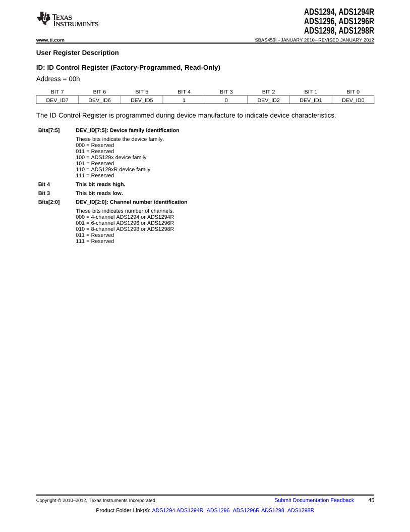
ADS1294, ADS1294RADS1296, ADS1296RADS1298, ADS1298R
www.ti.com SBAS459I –JANUARY 2010–REVISED JANUARY 2012
User Register Description
ID: ID Control Register (Factory-Programmed, Read-Only)
Address = 00h
BIT 7 BIT 6 BIT 5 BIT 4 BIT 3 BIT 2 BIT 1 BIT 0
DEV_ID7 DEV_ID6 DEV_ID5 1 0 DEV_ID2 DEV_ID1 DEV_ID0
The ID Control Register is programmed during device manufacture to indicate device characteristics.
Bits[7:5] DEV_ID[7:5]: Device family identification
These bits indicate the device family.000 = Reserved011 = Reserved100 = ADS129x device family101 = Reserved110 = ADS129xR device family111 = Reserved
Bit 4 This bit reads high.
Bit 3 This bit reads low.
Bits[2:0] DEV_ID[2:0]: Channel number identification
These bits indicates number of channels.000 = 4-channel ADS1294 or ADS1294R001 = 6-channel ADS1296 or ADS1296R010 = 8-channel ADS1298 or ADS1298R011 = Reserved111 = Reserved
Copyright © 2010–2012, Texas Instruments Incorporated Submit Documentation Feedback 45
Product Folder Link(s): ADS1294 ADS1294R ADS1296 ADS1296R ADS1298 ADS1298R
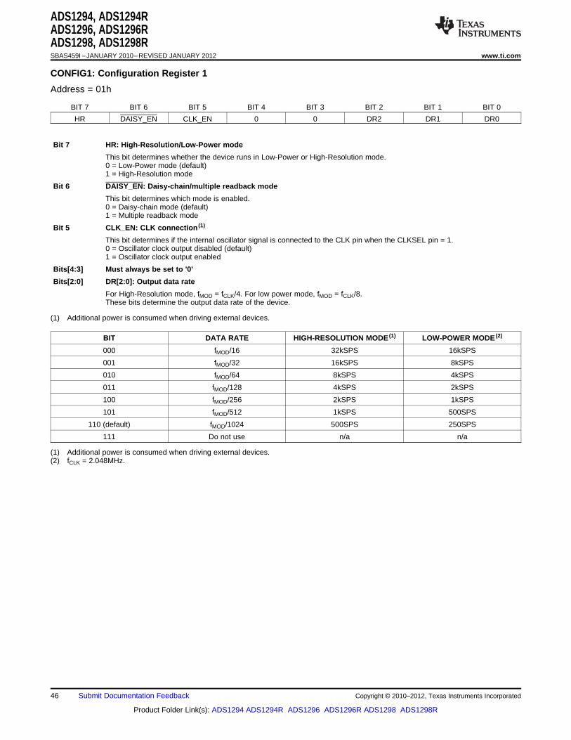
ADS1294, ADS1294RADS1296, ADS1296RADS1298, ADS1298RSBAS459I –JANUARY 2010–REVISED JANUARY 2012 www.ti.com
CONFIG1: Configuration Register 1
Address = 01h
BIT 7 BIT 6 BIT 5 BIT 4 BIT 3 BIT 2 BIT 1 BIT 0
HR DAISY_EN CLK_EN 0 0 DR2 DR1 DR0
Bit 7 HR: High-Resolution/Low-Power mode
This bit determines whether the device runs in Low-Power or High-Resolution mode.0 = Low-Power mode (default)1 = High-Resolution mode
Bit 6 DAISY_EN: Daisy-chain/multiple readback mode
This bit determines which mode is enabled.0 = Daisy-chain mode (default)1 = Multiple readback mode
Bit 5 CLK_EN: CLK connection (1)
This bit determines if the internal oscillator signal is connected to the CLK pin when the CLKSEL pin = 1.0 = Oscillator clock output disabled (default)1 = Oscillator clock output enabled
Bits[4:3] Must always be set to '0'
Bits[2:0] DR[2:0]: Output data rate
For High-Resolution mode, fMOD = fCLK/4. For low power mode, fMOD = fCLK/8.These bits determine the output data rate of the device.
(1) Additional power is consumed when driving external devices.
BIT DATA RATE HIGH-RESOLUTION MODE (1) LOW-POWER MODE (2)
000 fMOD/16 32kSPS 16kSPS
001 fMOD/32 16kSPS 8kSPS
010 fMOD/64 8kSPS 4kSPS
011 fMOD/128 4kSPS 2kSPS
100 fMOD/256 2kSPS 1kSPS
101 fMOD/512 1kSPS 500SPS
110 (default) fMOD/1024 500SPS 250SPS
111 Do not use n/a n/a
(1) Additional power is consumed when driving external devices.(2) fCLK = 2.048MHz.
46 Submit Documentation Feedback Copyright © 2010–2012, Texas Instruments Incorporated
Product Folder Link(s): ADS1294 ADS1294R ADS1296 ADS1296R ADS1298 ADS1298R
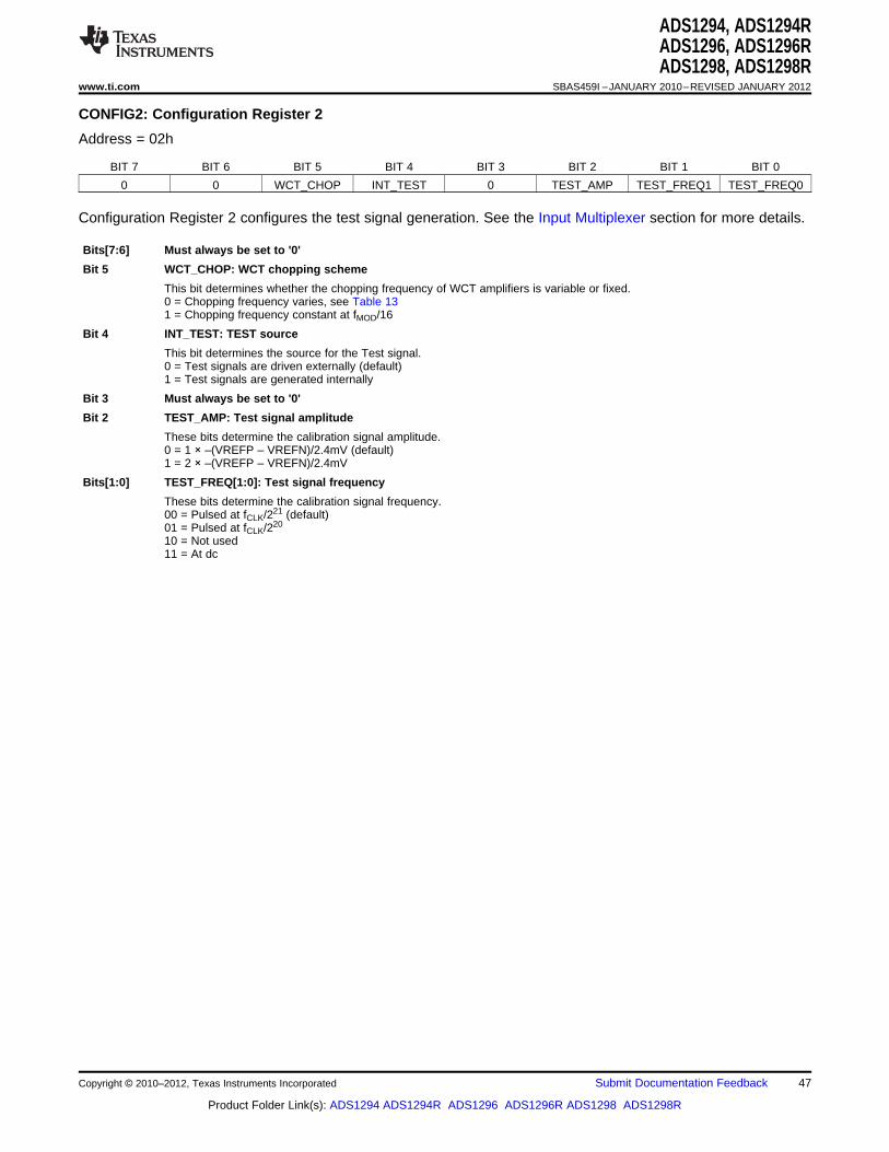
ADS1294, ADS1294RADS1296, ADS1296RADS1298, ADS1298R
www.ti.com SBAS459I –JANUARY 2010–REVISED JANUARY 2012
CONFIG2: Configuration Register 2
Address = 02h
BIT 7 BIT 6 BIT 5 BIT 4 BIT 3 BIT 2 BIT 1 BIT 0
0 0 WCT_CHOP INT_TEST 0 TEST_AMP TEST_FREQ1 TEST_FREQ0
Configuration Register 2 configures the test signal generation. See the Input Multiplexer section for more details.
Bits[7:6] Must always be set to '0'
Bit 5 WCT_CHOP: WCT chopping scheme
This bit determines whether the chopping frequency of WCT amplifiers is variable or fixed.0 = Chopping frequency varies, see Table 131 = Chopping frequency constant at fMOD/16
Bit 4 INT_TEST: TEST source
This bit determines the source for the Test signal.0 = Test signals are driven externally (default)1 = Test signals are generated internally
Bit 3 Must always be set to '0'
Bit 2 TEST_AMP: Test signal amplitude
These bits determine the calibration signal amplitude.0 = 1 × –(VREFP – VREFN)/2.4mV (default)1 = 2 × –(VREFP – VREFN)/2.4mV
Bits[1:0] TEST_FREQ[1:0]: Test signal frequency
These bits determine the calibration signal frequency.00 = Pulsed at fCLK/221 (default)01 = Pulsed at fCLK/220
10 = Not used11 = At dc
Copyright © 2010–2012, Texas Instruments Incorporated Submit Documentation Feedback 47
Product Folder Link(s): ADS1294 ADS1294R ADS1296 ADS1296R ADS1298 ADS1298R

ADS1294, ADS1294RADS1296, ADS1296RADS1298, ADS1298RSBAS459I –JANUARY 2010–REVISED JANUARY 2012 www.ti.com
CONFIG3: Configuration Register 3
Address = 03h
BIT 7 BIT 6 BIT 5 BIT 4 BIT 3 BIT 2 BIT 1 BIT 0
PD_REFBUF 1 VREF_4V RLD_MEAS RLDREF_INT PD_RLD RLD_LOFF_SENS RLD_STAT
Configuration Register 3 configures multi-reference and RLD operation.
Bit 7 PD_REFBUF: Power-down reference buffer
This bit determines the power-down reference buffer state.0 = Power-down internal reference buffer (default)1 = Enable internal reference buffer
Bit 6 Must always be set to '1'
Default is '1' at power-up.
Bit 5 VREF_4V: Reference voltage
This bit determines the reference voltage, VREFP.0 = VREFP is set to 2.4V (default)1 = VREFP is set to 4V (use only with a 5V analog supply)
Bit 4 RLD_MEAS: RLD measurement
This bit enables RLD measurement. The RLD signal may be measured with any channel.0 = Open (default)1 = RLD_IN signal is routed to the channel that has the MUX_Setting 010 (VREF)
Bit 3 RLDREF_INT: RLDREF signal
This bit determines the RLDREF signal source.0 = RLDREF signal fed externally (default)1 = RLDREF signal (AVDD – AVSS)/2 generated internally
Bit 2 PD_RLD: RLD buffer power
This bit determines the RLD buffer power state.0 = RLD buffer is powered down (default)1 = RLD buffer is enabled
Bit 1 RLD_LOFF_SENS: RLD sense function
This bit enables the RLD sense function.0 = RLD sense is disabled (default)1 = RLD sense is enabled
Bit 0 RLD_STAT: RLD lead-off status
This bit determines the RLD status.0 = RLD is connected (default)1 = RLD is not connected
48 Submit Documentation Feedback Copyright © 2010–2012, Texas Instruments Incorporated
Product Folder Link(s): ADS1294 ADS1294R ADS1296 ADS1296R ADS1298 ADS1298R
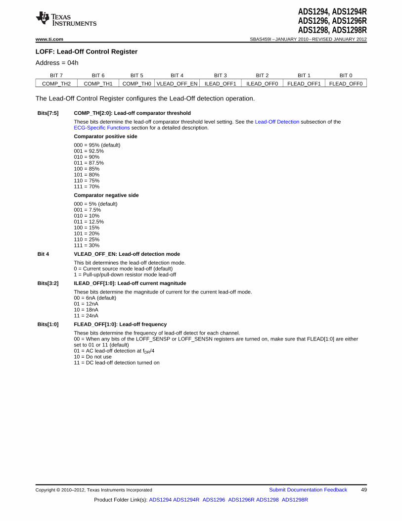
ADS1294, ADS1294RADS1296, ADS1296RADS1298, ADS1298R
www.ti.com SBAS459I –JANUARY 2010–REVISED JANUARY 2012
LOFF: Lead-Off Control Register
Address = 04h
BIT 7 BIT 6 BIT 5 BIT 4 BIT 3 BIT 2 BIT 1 BIT 0
COMP_TH2 COMP_TH1 COMP_TH0 VLEAD_OFF_EN ILEAD_OFF1 ILEAD_OFF0 FLEAD_OFF1 FLEAD_OFF0
The Lead-Off Control Register configures the Lead-Off detection operation.
Bits[7:5] COMP_TH[2:0]: Lead-off comparator threshold
These bits determine the lead-off comparator threshold level setting. See the Lead-Off Detection subsection of theECG-Specific Functions section for a detailed description.
Comparator positive side
000 = 95% (default)001 = 92.5%010 = 90%011 = 87.5%100 = 85%101 = 80%110 = 75%111 = 70%
Comparator negative side
000 = 5% (default)001 = 7.5%010 = 10%011 = 12.5%100 = 15%101 = 20%110 = 25%111 = 30%
Bit 4 VLEAD_OFF_EN: Lead-off detection mode
This bit determines the lead-off detection mode.0 = Current source mode lead-off (default)1 = Pull-up/pull-down resistor mode lead-off
Bits[3:2] ILEAD_OFF[1:0]: Lead-off current magnitude
These bits determine the magnitude of current for the current lead-off mode.00 = 6nA (default)01 = 12nA10 = 18nA11 = 24nA
Bits[1:0] FLEAD_OFF[1:0]: Lead-off frequency
These bits determine the frequency of lead-off detect for each channel.00 = When any bits of the LOFF_SENSP or LOFF_SENSN registers are turned on, make sure that FLEAD[1:0] are eitherset to 01 or 11 (default)01 = AC lead-off detection at fDR/410 = Do not use11 = DC lead-off detection turned on
Copyright © 2010–2012, Texas Instruments Incorporated Submit Documentation Feedback 49
Product Folder Link(s): ADS1294 ADS1294R ADS1296 ADS1296R ADS1298 ADS1298R
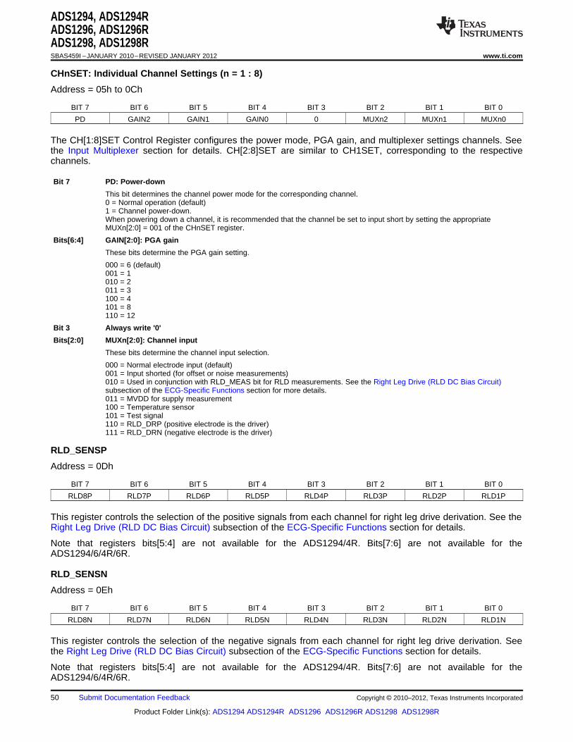
ADS1294, ADS1294RADS1296, ADS1296RADS1298, ADS1298RSBAS459I –JANUARY 2010–REVISED JANUARY 2012 www.ti.com
CHnSET: Individual Channel Settings (n = 1 : 8)
Address = 05h to 0Ch
BIT 7 BIT 6 BIT 5 BIT 4 BIT 3 BIT 2 BIT 1 BIT 0
PD GAIN2 GAIN1 GAIN0 0 MUXn2 MUXn1 MUXn0
The CH[1:8]SET Control Register configures the power mode, PGA gain, and multiplexer settings channels. Seethe Input Multiplexer section for details. CH[2:8]SET are similar to CH1SET, corresponding to the respectivechannels.
Bit 7 PD: Power-down
This bit determines the channel power mode for the corresponding channel.0 = Normal operation (default)1 = Channel power-down.When powering down a channel, it is recommended that the channel be set to input short by setting the appropriateMUXn[2:0] = 001 of the CHnSET register.
Bits[6:4] GAIN[2:0]: PGA gain
These bits determine the PGA gain setting.
000 = 6 (default)001 = 1010 = 2011 = 3100 = 4101 = 8110 = 12
Bit 3 Always write '0'
Bits[2:0] MUXn[2:0]: Channel input
These bits determine the channel input selection.
000 = Normal electrode input (default)001 = Input shorted (for offset or noise measurements)010 = Used in conjunction with RLD_MEAS bit for RLD measurements. See the Right Leg Drive (RLD DC Bias Circuit)subsection of the ECG-Specific Functions section for more details.011 = MVDD for supply measurement100 = Temperature sensor101 = Test signal110 = RLD_DRP (positive electrode is the driver)111 = RLD_DRN (negative electrode is the driver)
RLD_SENSP
Address = 0Dh
BIT 7 BIT 6 BIT 5 BIT 4 BIT 3 BIT 2 BIT 1 BIT 0
RLD8P RLD7P RLD6P RLD5P RLD4P RLD3P RLD2P RLD1P
This register controls the selection of the positive signals from each channel for right leg drive derivation. See theRight Leg Drive (RLD DC Bias Circuit) subsection of the ECG-Specific Functions section for details.
Note that registers bits[5:4] are not available for the ADS1294/4R. Bits[7:6] are not available for theADS1294/6/4R/6R.
RLD_SENSN
Address = 0Eh
BIT 7 BIT 6 BIT 5 BIT 4 BIT 3 BIT 2 BIT 1 BIT 0
RLD8N RLD7N RLD6N RLD5N RLD4N RLD3N RLD2N RLD1N
This register controls the selection of the negative signals from each channel for right leg drive derivation. Seethe Right Leg Drive (RLD DC Bias Circuit) subsection of the ECG-Specific Functions section for details.
Note that registers bits[5:4] are not available for the ADS1294/4R. Bits[7:6] are not available for theADS1294/6/4R/6R.
50 Submit Documentation Feedback Copyright © 2010–2012, Texas Instruments Incorporated
Product Folder Link(s): ADS1294 ADS1294R ADS1296 ADS1296R ADS1298 ADS1298R
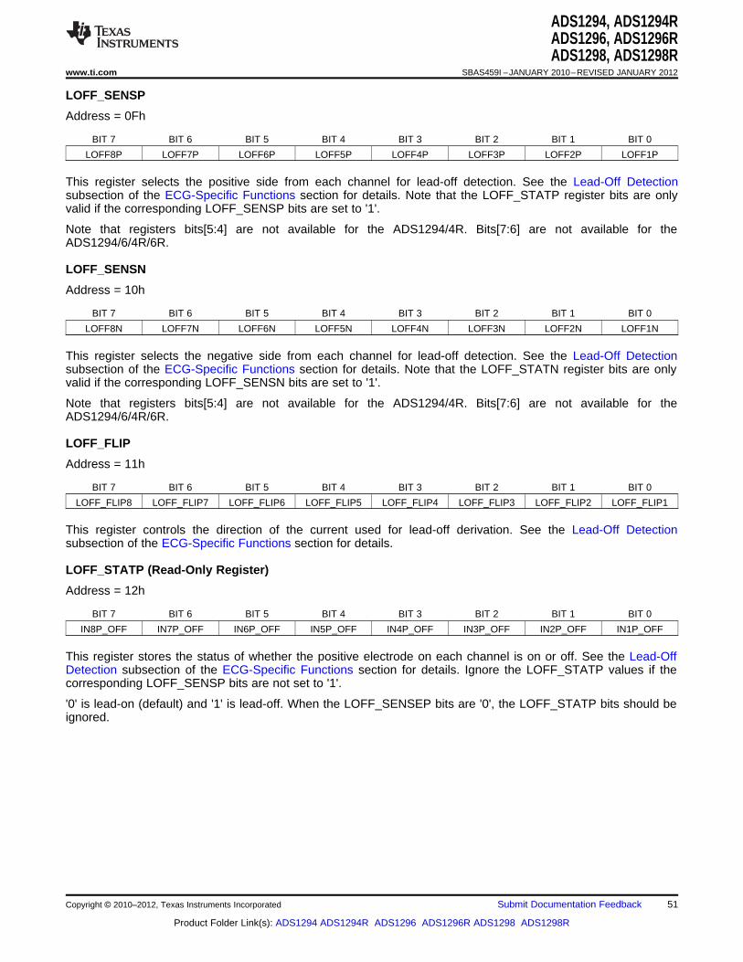
ADS1294, ADS1294RADS1296, ADS1296RADS1298, ADS1298R
www.ti.com SBAS459I –JANUARY 2010–REVISED JANUARY 2012
LOFF_SENSP
Address = 0Fh
BIT 7 BIT 6 BIT 5 BIT 4 BIT 3 BIT 2 BIT 1 BIT 0
LOFF8P LOFF7P LOFF6P LOFF5P LOFF4P LOFF3P LOFF2P LOFF1P
This register selects the positive side from each channel for lead-off detection. See the Lead-Off Detectionsubsection of the ECG-Specific Functions section for details. Note that the LOFF_STATP register bits are onlyvalid if the corresponding LOFF_SENSP bits are set to '1'.
Note that registers bits[5:4] are not available for the ADS1294/4R. Bits[7:6] are not available for theADS1294/6/4R/6R.
LOFF_SENSN
Address = 10h
BIT 7 BIT 6 BIT 5 BIT 4 BIT 3 BIT 2 BIT 1 BIT 0
LOFF8N LOFF7N LOFF6N LOFF5N LOFF4N LOFF3N LOFF2N LOFF1N
This register selects the negative side from each channel for lead-off detection. See the Lead-Off Detectionsubsection of the ECG-Specific Functions section for details. Note that the LOFF_STATN register bits are onlyvalid if the corresponding LOFF_SENSN bits are set to '1'.
Note that registers bits[5:4] are not available for the ADS1294/4R. Bits[7:6] are not available for theADS1294/6/4R/6R.
LOFF_FLIP
Address = 11h
BIT 7 BIT 6 BIT 5 BIT 4 BIT 3 BIT 2 BIT 1 BIT 0
LOFF_FLIP8 LOFF_FLIP7 LOFF_FLIP6 LOFF_FLIP5 LOFF_FLIP4 LOFF_FLIP3 LOFF_FLIP2 LOFF_FLIP1
This register controls the direction of the current used for lead-off derivation. See the Lead-Off Detectionsubsection of the ECG-Specific Functions section for details.
LOFF_STATP (Read-Only Register)
Address = 12h
BIT 7 BIT 6 BIT 5 BIT 4 BIT 3 BIT 2 BIT 1 BIT 0
IN8P_OFF IN7P_OFF IN6P_OFF IN5P_OFF IN4P_OFF IN3P_OFF IN2P_OFF IN1P_OFF
This register stores the status of whether the positive electrode on each channel is on or off. See the Lead-OffDetection subsection of the ECG-Specific Functions section for details. Ignore the LOFF_STATP values if thecorresponding LOFF_SENSP bits are not set to '1'.
'0' is lead-on (default) and '1' is lead-off. When the LOFF_SENSEP bits are '0', the LOFF_STATP bits should beignored.
Copyright © 2010–2012, Texas Instruments Incorporated Submit Documentation Feedback 51
Product Folder Link(s): ADS1294 ADS1294R ADS1296 ADS1296R ADS1298 ADS1298R
ADS1294, ADS1294RADS1296, ADS1296RADS1298, ADS1298RSBAS459I –JANUARY 2010–REVISED JANUARY 2012 www.ti.com
LOFF_STATN (Read-Only Register)
Address = 13h
BIT 7 BIT 6 BIT 5 BIT 4 BIT 3 BIT 2 BIT 1 BIT 0
IN8N_OFF IN7N_OFF IN6N_OFF IN5N_OFF IN4N_OFF IN3N_OFF IN2N_OFF IN1N_OFF
This register stores the status of whether the negative electrode on each channel is on or off. See the Lead-OffDetection subsection of the ECG-Specific Functions section for details. Ignore the LOFF_STATN values if thecorresponding LOFF_SENSN bits are not set to '1'.
'0' is lead-on (default) and '1' is lead-off. When the LOFF_SENSEN bits are '0', the LOFF_STATP bits should beignored.
GPIO: General-Purpose I/O Register
Address = 14h
BIT 7 BIT 6 BIT 5 BIT 4 BIT 3 BIT 2 BIT 1 BIT 0
GPIOD4 GPIOD3 GPIOD2 GPIOD1 GPIOC4 GPIOC3 GPIOC2 GPIOC1
The General-Purpose I/O Register controls the action of the three GPIO pins. Note that when RESP_CTRL[1:0]is in mode 01 and 11, the GPIO2, GPIO3, and GPIO4 pins are not available for use.
Bits[7:4] GPIOD[4:1]: GPIO data
These bits are used to read and write data to the GPIO ports.When reading the register, the data returned correspond to the state of the GPIO external pins, whether they areprogrammed as inputs or as outputs. As outputs, a write to the GPIOD sets the output value. As inputs, a write to theGPIOD has no effect. GPIO is not available in certain respiration modes.
Bits[3:0] GPIOC[4:1]: GPIO control (corresponding GPIOD)
These bits determine if the corresponding GPIOD pin is an input or output.0 = Output1 = Input (default)
PACE: PACE Detect Register
Address = 15h
BIT 7 BIT 6 BIT 5 BIT 4 BIT 3 BIT 2 BIT 1 BIT 0
0 0 0 PACEE1 PACEE0 PACEO1 PACEO0 PD_PACE
This register provides the PACE controls that configure the channel signal used to feed the external PACE detectcircuitry. See the Pace Detect subsection of the ECG-Specific Functions section for details.
Bits[7:5] Must always be set to '0'
Bits[4:3] PACEE[1:0]: PACE even channels
These bits control the selection of the even number channels available on TEST_PACE_OUT1. Note that only one channelmay be selected at any time.00 = Channel 2 (default)01 = Channel 410 = Channel 6, ADS1296/8/6R/8R only11 = Channel 8, ADS1298/8R only
Bits[2:1] PACEO[1:0]: PACE odd channels
These bits control the selection of the odd number channels available on TEST_PACE_OUT2. Note that only one channelmay be selected at any time.00 = Channel 1 (default)01 = Channel 310 = Channel 5, ADS1296/8/6R/8R only11 = Channel 7, ADS1298/8R only
Bit 0 PD_PACE: PACE detect buffer
This bit is used to enable/disable the PACE detect buffer.0 = PACE detect buffer turned off (default)1 = PACE detect buffer turned on
52 Submit Documentation Feedback Copyright © 2010–2012, Texas Instruments Incorporated
Product Folder Link(s): ADS1294 ADS1294R ADS1296 ADS1296R ADS1298 ADS1298R
ADS1294, ADS1294RADS1296, ADS1296RADS1298, ADS1298R
www.ti.com SBAS459I –JANUARY 2010–REVISED JANUARY 2012
RESP: Respiration Control Register
Address = 16h
BIT 7 BIT 6 BIT 5 BIT 4 BIT 3 BIT 2 BIT 1 BIT 0
RESP_ RESP_MOD_ 1 RESP_PH2 RESP_PH1 RESP_PH0 RESP_CTRL1 RESP_CTRL0DEMOD_EN1 EN1
This register provides the controls for the respiration circuitry; see the Respiration section for details.
Bit 7 RESP_DEMOD_EN1: Enables respiration demodulation circuitry (ADS1294R/6R/8R only, for ADS1294/6/8 alwayswrite '0')
This bit enables/disables the demodulation circuitry on channel 1.0 = RESP demodulation circuitry turned off (default)1 = RESP demodulation circuitry turned on
Bit 6 RESP_MOD_EN1: Enables respiration modulation circuitry (ADS1294R/6R/8R only, for ADS1294/6/8 always write '0')
This bit enables/disables the modulation circuitry on channel 1.0 = RESP modulation circuitry turned off (default)1 = RESP modulation circuitry turned on
Bit 5 Reserved
Must always be set to '1' for ADS1294R/6R/8R. This bit does not have any effect for the ADS1294/6/8.
Bits[4:2] RESP_PH[2:0]: Respiration phase (1)
These bits control the phase of the respiration demodulation control signal. (GPIO4 is out-of-phase with GPIO3 by thephase determined by the RESP_PH bits.)
000 = 22.5° (default)001 = 45°010 = 67.5°011 = 90°100 = 112.5°101 = 135°110 = 157.5°111 = N/A
Bits[1:0] RESP_CTRL[1:0]: Respiration control
These bits set the mode of the respiration circuitry.00 = No respiration (default)01= External respiration10 = Internal respiration with internal signals11 = Internal respiration with user-generated signals
(1) RESP_PH[2:0] phase control bits only for internal respiration (RESP_CTRL = 10) and external respiration (RESP_CTRL = 01) modeswhen the CONFIG4.RESP_FREQ[2:0] register bits are 000b or 001b.
Copyright © 2010–2012, Texas Instruments Incorporated Submit Documentation Feedback 53
Product Folder Link(s): ADS1294 ADS1294R ADS1296 ADS1296R ADS1298 ADS1298R
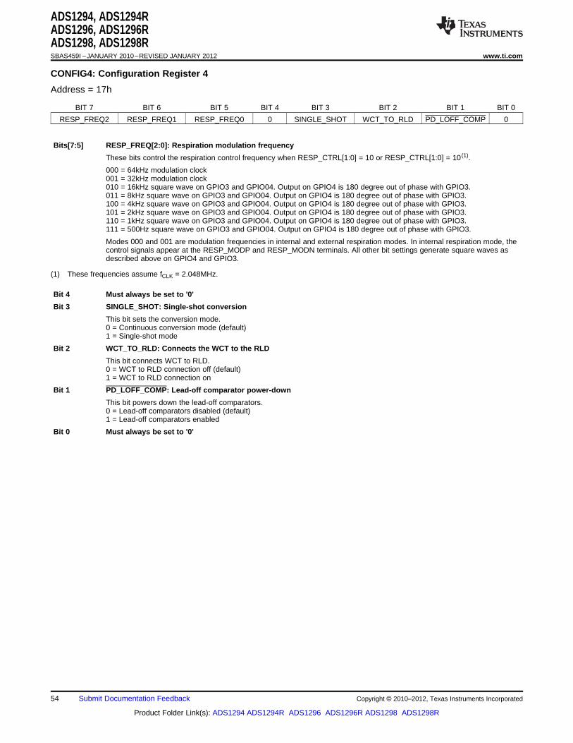
ADS1294, ADS1294RADS1296, ADS1296RADS1298, ADS1298RSBAS459I –JANUARY 2010–REVISED JANUARY 2012 www.ti.com
CONFIG4: Configuration Register 4
Address = 17h
BIT 7 BIT 6 BIT 5 BIT 4 BIT 3 BIT 2 BIT 1 BIT 0
RESP_FREQ2 RESP_FREQ1 RESP_FREQ0 0 SINGLE_SHOT WCT_TO_RLD PD_LOFF_COMP 0
Bits[7:5] RESP_FREQ[2:0]: Respiration modulation frequency
These bits control the respiration control frequency when RESP_CTRL[1:0] = 10 or RESP_CTRL[1:0] = 10 (1).
000 = 64kHz modulation clock001 = 32kHz modulation clock010 = 16kHz square wave on GPIO3 and GPIO04. Output on GPIO4 is 180 degree out of phase with GPIO3.011 = 8kHz square wave on GPIO3 and GPIO04. Output on GPIO4 is 180 degree out of phase with GPIO3.100 = 4kHz square wave on GPIO3 and GPIO04. Output on GPIO4 is 180 degree out of phase with GPIO3.101 = 2kHz square wave on GPIO3 and GPIO04. Output on GPIO4 is 180 degree out of phase with GPIO3.110 = 1kHz square wave on GPIO3 and GPIO04. Output on GPIO4 is 180 degree out of phase with GPIO3.111 = 500Hz square wave on GPIO3 and GPIO04. Output on GPIO4 is 180 degree out of phase with GPIO3.
Modes 000 and 001 are modulation frequencies in internal and external respiration modes. In internal respiration mode, thecontrol signals appear at the RESP_MODP and RESP_MODN terminals. All other bit settings generate square waves asdescribed above on GPIO4 and GPIO3.
(1) These frequencies assume fCLK = 2.048MHz.
Bit 4 Must always be set to '0'
Bit 3 SINGLE_SHOT: Single-shot conversion
This bit sets the conversion mode.0 = Continuous conversion mode (default)1 = Single-shot mode
Bit 2 WCT_TO_RLD: Connects the WCT to the RLD
This bit connects WCT to RLD.0 = WCT to RLD connection off (default)1 = WCT to RLD connection on
Bit 1 PD_LOFF_COMP: Lead-off comparator power-down
This bit powers down the lead-off comparators.0 = Lead-off comparators disabled (default)1 = Lead-off comparators enabled
Bit 0 Must always be set to '0'
54 Submit Documentation Feedback Copyright © 2010–2012, Texas Instruments Incorporated
Product Folder Link(s): ADS1294 ADS1294R ADS1296 ADS1296R ADS1298 ADS1298R
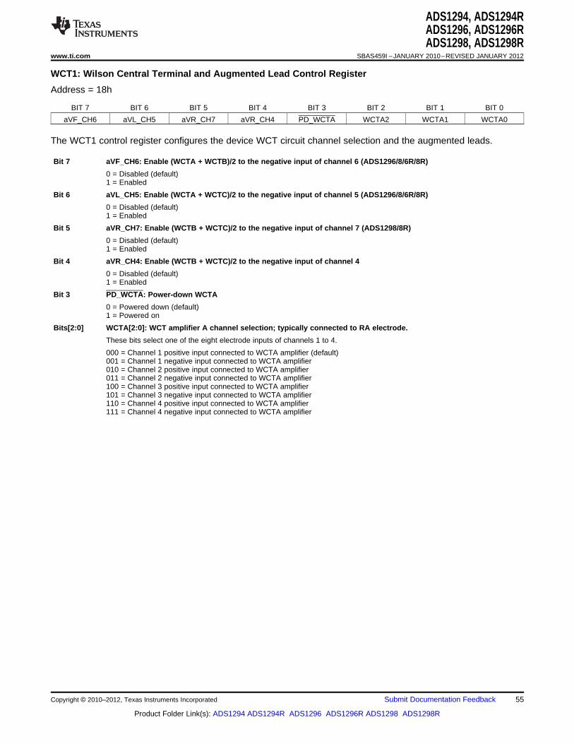
ADS1294, ADS1294RADS1296, ADS1296RADS1298, ADS1298R
www.ti.com SBAS459I –JANUARY 2010–REVISED JANUARY 2012
WCT1: Wilson Central Terminal and Augmented Lead Control Register
Address = 18h
BIT 7 BIT 6 BIT 5 BIT 4 BIT 3 BIT 2 BIT 1 BIT 0
aVF_CH6 aVL_CH5 aVR_CH7 aVR_CH4 PD_WCTA WCTA2 WCTA1 WCTA0
The WCT1 control register configures the device WCT circuit channel selection and the augmented leads.
Bit 7 aVF_CH6: Enable (WCTA + WCTB)/2 to the negative input of channel 6 (ADS1296/8/6R/8R)
0 = Disabled (default)1 = Enabled
Bit 6 aVL_CH5: Enable (WCTA + WCTC)/2 to the negative input of channel 5 (ADS1296/8/6R/8R)
0 = Disabled (default)1 = Enabled
Bit 5 aVR_CH7: Enable (WCTB + WCTC)/2 to the negative input of channel 7 (ADS1298/8R)
0 = Disabled (default)1 = Enabled
Bit 4 aVR_CH4: Enable (WCTB + WCTC)/2 to the negative input of channel 4
0 = Disabled (default)1 = Enabled
Bit 3 PD_WCTA: Power-down WCTA
0 = Powered down (default)1 = Powered on
Bits[2:0] WCTA[2:0]: WCT amplifier A channel selection; typically connected to RA electrode.
These bits select one of the eight electrode inputs of channels 1 to 4.
000 = Channel 1 positive input connected to WCTA amplifier (default)001 = Channel 1 negative input connected to WCTA amplifier010 = Channel 2 positive input connected to WCTA amplifier011 = Channel 2 negative input connected to WCTA amplifier100 = Channel 3 positive input connected to WCTA amplifier101 = Channel 3 negative input connected to WCTA amplifier110 = Channel 4 positive input connected to WCTA amplifier111 = Channel 4 negative input connected to WCTA amplifier
Copyright © 2010–2012, Texas Instruments Incorporated Submit Documentation Feedback 55
Product Folder Link(s): ADS1294 ADS1294R ADS1296 ADS1296R ADS1298 ADS1298R
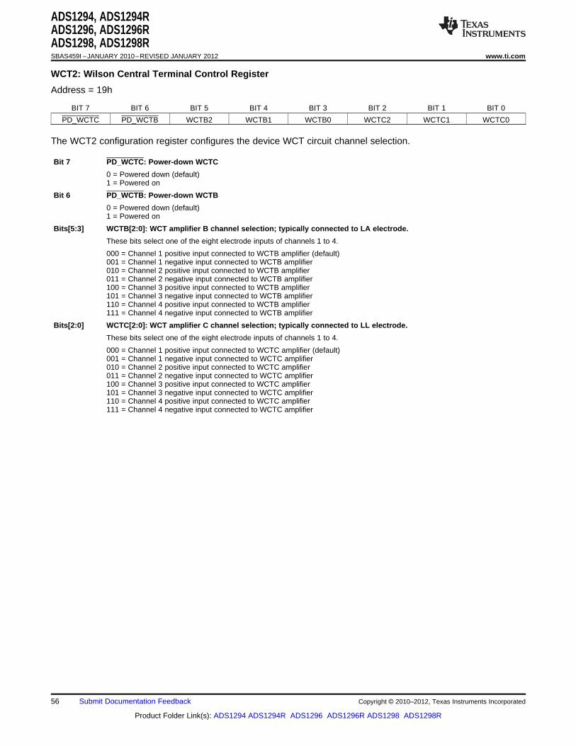
ADS1294, ADS1294RADS1296, ADS1296RADS1298, ADS1298RSBAS459I –JANUARY 2010–REVISED JANUARY 2012 www.ti.com
WCT2: Wilson Central Terminal Control Register
Address = 19h
BIT 7 BIT 6 BIT 5 BIT 4 BIT 3 BIT 2 BIT 1 BIT 0
PD_WCTC PD_WCTB WCTB2 WCTB1 WCTB0 WCTC2 WCTC1 WCTC0
The WCT2 configuration register configures the device WCT circuit channel selection.
Bit 7 PD_WCTC: Power-down WCTC
0 = Powered down (default)1 = Powered on
Bit 6 PD_WCTB: Power-down WCTB
0 = Powered down (default)1 = Powered on
Bits[5:3] WCTB[2:0]: WCT amplifier B channel selection; typically connected to LA electrode.
These bits select one of the eight electrode inputs of channels 1 to 4.
000 = Channel 1 positive input connected to WCTB amplifier (default)001 = Channel 1 negative input connected to WCTB amplifier010 = Channel 2 positive input connected to WCTB amplifier011 = Channel 2 negative input connected to WCTB amplifier100 = Channel 3 positive input connected to WCTB amplifier101 = Channel 3 negative input connected to WCTB amplifier110 = Channel 4 positive input connected to WCTB amplifier111 = Channel 4 negative input connected to WCTB amplifier
Bits[2:0] WCTC[2:0]: WCT amplifier C channel selection; typically connected to LL electrode.
These bits select one of the eight electrode inputs of channels 1 to 4.
000 = Channel 1 positive input connected to WCTC amplifier (default)001 = Channel 1 negative input connected to WCTC amplifier010 = Channel 2 positive input connected to WCTC amplifier011 = Channel 2 negative input connected to WCTC amplifier100 = Channel 3 positive input connected to WCTC amplifier101 = Channel 3 negative input connected to WCTC amplifier110 = Channel 4 positive input connected to WCTC amplifier111 = Channel 4 negative input connected to WCTC amplifier
56 Submit Documentation Feedback Copyright © 2010–2012, Texas Instruments Incorporated
Product Folder Link(s): ADS1294 ADS1294R ADS1296 ADS1296R ADS1298 ADS1298R
MUX1[2:0] = 000
RLD_SENSP[0] = 1
RLD_SENSN[0] = 1
MUX2[2:0] = 000
MUX3[2:0] = 000
MUX8[2:0] = 111
PGA1
RLD_SENSP[1] = 1
RLD_SENSN[1] = 1PGA2
RLD_SENSP[2] = 1
RLD_SENSN[2] = 1PGA3
RLD_AMP
RLD_SENSP[7] = 0
RLD_SENSN[7] = 0PGA8
RLDOUT RLDINVRLDREFRLDIN
Filter or
Feedthrough
ADS1298
¼ ¼
MUX
EMI
Filter
EMI
Filter
EMI
Filter
EMI
Filter
IN1P
¼
IN1N
IN2P
IN3P
IN8P
IN2N
IN3N
IN8N
1MW(1)
1.5nF(1)
RLDREF_INT
(AVDD + AVSS)/2
RLD
RE
F_IN
T
ADS1294, ADS1294RADS1296, ADS1296RADS1298, ADS1298R
www.ti.com SBAS459I –JANUARY 2010–REVISED JANUARY 2012
ECG-SPECIFIC FUNCTIONS
INPUT MULTIPLEXER (REROUTING THE RIGHT LEG DRIVE SIGNAL)
The input multiplexer has ECG-specific functions for the right leg drive signal. The RLD signal is available at theRLDOUT pin once the appropriate channels are selected for the RLD derivation, feedback elements are installedexternal to the chip, and the loop is closed. This signal can be fed after filtering or fed directly into the RLDIN pinas shown in Figure 51. This RLDIN signal can be multiplexed into any one of the input electrodes by setting theMUX bits of the appropriate channel set registers to 110 for P-side or 111 for N-side. Figure 51 shows the RLDsignal generated from channels 1, 2, and 3 and routed to the N-side of channel 8. This feature can be used todynamically change the electrode that is used as the reference signal to drive the patient body. Note that thecorresponding channel cannot be used and can be powered down.
(1) Typical values for example only.
Figure 51. Example of RLDOUT Signal Configured to be Routed to IN8N
Copyright © 2010–2012, Texas Instruments Incorporated Submit Documentation Feedback 57
Product Folder Link(s): ADS1294 ADS1294R ADS1296 ADS1296R ADS1298 ADS1298R

MUX1[2:0] = 000
RLD_SENSP[0] = 1
RLD_SENSN[0] = 1
MUX2[2:0] = 000
MUX3[2:0] = 000
MUX8[2:0] = 010
RLD_MEAS = 1AND
PGA1
RLD_SENSP[1] = 1
RLD_SENSN[1] = 1PGA2
RLD_SENSP[2] = 1
RLD_SENSN[2] = 1PGA3
RLD_AMP
RLD_SENSP[7] = 0
RLD_SENSN[7] = 0PGA8
RLD_OUT RLD_INVRLD_REFRLD_IN
Filter or
Feedthrough
ADS1298
¼ ¼
IN1P
IN1N
EMI
Filter
MUX
EMI
Filter
EMI
Filter
EMI
Filter
¼
IN2N
IN3N
IN8N
IN2P
IN3P
IN8P
MUX8 010[2:0] =
1MW(1)
1.5nF(1)
RLDREF_INT
RLD
RE
F_IN
T
(AVDD + AVSS)/2
ADS1294, ADS1294RADS1296, ADS1296RADS1298, ADS1298RSBAS459I –JANUARY 2010–REVISED JANUARY 2012 www.ti.com
INPUT MULTIPLEXER (MEASURING THE RIGHT LEG DRIVE SIGNAL)
Also, the RLDOUT signal can be routed to a channel (that is not used for the calculation of RLD) formeasurement. Figure 52 shows the register settings to route the RLDIN signal to channel 8. The measurement isdone with respect to the voltage on the RLDREF pin. If RLDREF is chosen to be internal, it would be at (AVDD +AVSS)/2. This feature is useful for debugging purposes during product development.
(1) Typical values for example only.
Figure 52. RLDOUT Signal Configured to be Read Back by Channel 8
58 Submit Documentation Feedback Copyright © 2010–2012, Texas Instruments Incorporated
Product Folder Link(s): ADS1294 ADS1294R ADS1296 ADS1296R ADS1298 ADS1298R
Wcta
8:1 MUX
WC
T1[2
:0]
IN4N
IN4P
IN3N
IN3P
IN2N
IN2P
WCT
IN1N
IN1P
Wctb
8:1 MUX
WC
T2[5
:3]
Wctc
8:1 MUX
WC
T2[2
:0]
To Channel
PGAs
ADS1294/6/8
30kW 30kW 30kW
80pF
AVSS
ADS1294, ADS1294RADS1296, ADS1296RADS1298, ADS1298R
www.ti.com SBAS459I –JANUARY 2010–REVISED JANUARY 2012
WILSON CENTRAL TERMINAL (WCT) AND CHEST LEADS
In the standard 12-lead ECG, WCT voltage is defined as the average of Right Arm (RA), Left Arm (LA), and LeftLeg (LL) electrodes. This voltage is used as the reference voltage for the measurement of the chest leads. TheADS129x has three integrated low-noise amplifiers that generate the WCT voltage. Figure 53 shows the blockdiagram of the implementation.
Figure 53. WCT Voltage
The devices provide flexibility to choose any one of the eight signals (IN1P to IN4N) to be routed to each of theamplifiers to generate the average. Having this flexibility allows the RA, LA, and LL electrodes to be connected toany input of the first four channels depending on the lead configuration.
Each of the three amplifiers in the WCT circuitry can be powered down individually with register settings. Bypowering up two amplifiers, the average of any two electrodes can be generated at the WCT pin. Powering upone amplifier provides the buffered electrode voltage at the WCT pin. Note that the WCT amplifiers have limiteddrive strength and thus should be buffered if used to drive a low-impedance load.
See Table 5 for performance when using any 1, 2, or 3 of the WCT buffers.
As can be seen in Table 5, the overall noise reduces when more than one WCT amplifier is powered up. Thisnoise reduction is a result of the fact that noise is averaged by the passive summing network at the output of theamplifiers. Powering down individual buffers gives negligible power savings because a significant portion of thecircuitry is shared between the three amplifiers. The bandwidth of the WCT node is limited by the RC network.The internal summing network consists of three 30kΩ resistors and a 80pF capacitor. It is recommended that anexternal 100pF capacitor be added for optimal performance. The effective bandwidth depends on the number ofamplifiers that are powered up, as shown in Table 5.
The WCT node should be only be used to drive very high input impedances (typically greater than 500MΩ).Typical application would be to connect this WCT signal to the negative inputs of a ADS129x to be used as areference signal for the chest leads.
Copyright © 2010–2012, Texas Instruments Incorporated Submit Documentation Feedback 59
Product Folder Link(s): ADS1294 ADS1294R ADS1296 ADS1296R ADS1298 ADS1298R
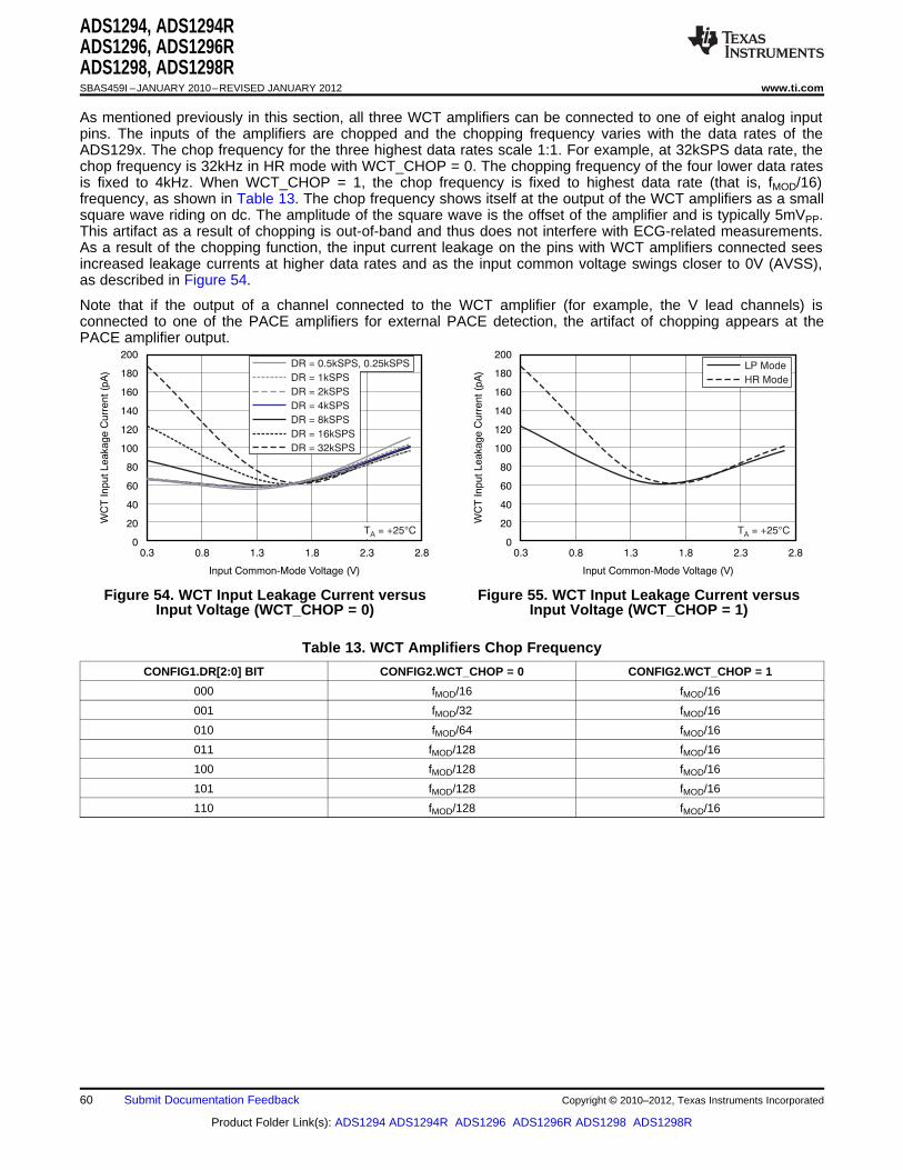
200
180
160
140
120
100
80
60
40
20
00.3 2.8
Input Common-Mode Voltage (V)
WC
T Input Leakage C
urr
ent (p
A)
0.8
T = +25 C°A
1.3 1.8 2.3
DR = 0.5kSPS, 0.25kSPS
DR = 1kSPS
DR = 2kSPS
DR = 4kSPS
DR = 8kSPS
DR = 16kSPS
DR = 32kSPS
200
180
160
140
120
100
80
60
40
20
00.3 2.8
Input Common-Mode Voltage (V)
WC
T Input Leakage C
urr
ent (p
A)
0.8
T = +25 C°A
LP Mode
HR Mode
1.3 1.8 2.3
ADS1294, ADS1294RADS1296, ADS1296RADS1298, ADS1298RSBAS459I –JANUARY 2010–REVISED JANUARY 2012 www.ti.com
As mentioned previously in this section, all three WCT amplifiers can be connected to one of eight analog inputpins. The inputs of the amplifiers are chopped and the chopping frequency varies with the data rates of theADS129x. The chop frequency for the three highest data rates scale 1:1. For example, at 32kSPS data rate, thechop frequency is 32kHz in HR mode with WCT_CHOP = 0. The chopping frequency of the four lower data ratesis fixed to 4kHz. When WCT_CHOP = 1, the chop frequency is fixed to highest data rate (that is, fMOD/16)frequency, as shown in Table 13. The chop frequency shows itself at the output of the WCT amplifiers as a smallsquare wave riding on dc. The amplitude of the square wave is the offset of the amplifier and is typically 5mVPP.This artifact as a result of chopping is out-of-band and thus does not interfere with ECG-related measurements.As a result of the chopping function, the input current leakage on the pins with WCT amplifiers connected seesincreased leakage currents at higher data rates and as the input common voltage swings closer to 0V (AVSS),as described in Figure 54.
Note that if the output of a channel connected to the WCT amplifier (for example, the V lead channels) isconnected to one of the PACE amplifiers for external PACE detection, the artifact of chopping appears at thePACE amplifier output.
Figure 54. WCT Input Leakage Current versus Figure 55. WCT Input Leakage Current versusInput Voltage (WCT_CHOP = 0) Input Voltage (WCT_CHOP = 1)
Table 13. WCT Amplifiers Chop Frequency
CONFIG1.DR[2:0] BIT CONFIG2.WCT_CHOP = 0 CONFIG2.WCT_CHOP = 1
000 fMOD/16 fMOD/16
001 fMOD/32 fMOD/16
010 fMOD/64 fMOD/16
011 fMOD/128 fMOD/16
100 fMOD/128 fMOD/16
101 fMOD/128 fMOD/16
110 fMOD/128 fMOD/16
60 Submit Documentation Feedback Copyright © 2010–2012, Texas Instruments Incorporated
Product Folder Link(s): ADS1294 ADS1294R ADS1296 ADS1296R ADS1298 ADS1298R

Wcta
8:1 MUX
WC
T1[2
:0]
IN4N
IN4P
IN3N
IN3P
IN2N
IN2P
IN7N
IN7P
IN6N
IN6P
IN5N
IN5P
IN1N
IN1P
Wctb
8:1 MUX
WC
T2[5
:3]
Wctc
8:1 MUXW
CT
2[2
:0]
To ChannelPGAs
ADS1298
avF_ch6 avF_ch5 avF_ch7
avF_ch4
To ChannelPGAs
ADS1294, ADS1294RADS1296, ADS1296RADS1298, ADS1298R
www.ti.com SBAS459I –JANUARY 2010–REVISED JANUARY 2012
Augmented Leads
In the typical implementation of the 12-lead ECG with eight channels, the augmented leads are calculateddigitally. In certain applications, it may be required that all leads be derived in analog rather than digital. TheADS1298/8R provides the option to generate the augmented leads by routing appropriate averages to channels5 to 7. The same three amplifiers that are used to generate the WCT signal are used to generate the GoldbergerCentral Terminal signals as well. Figure 56 shows an example of generating the augmented leads in analogdomain. Note that in this implementation it takes more than eight channels to generate the standard 12 leads.Also, this feature is not available in the ADS1296/6R and ADS1294/4R.
Figure 56. Analog Domain Augmented Leads
Right Leg Drive with the WCT Point
In certain applications, the out-of-phase version of the WCT is used as the right leg drive reference. TheADS1298 provides the option to have a buffered version of the WCT terminal at the RLD_OUT pin. This signalcan be inverted in phase using an external amplifier and used as the right leg drive. Refer to the Right Leg Drive(RLD DC Bias Circuit) section for more details.
Copyright © 2010–2012, Texas Instruments Incorporated Submit Documentation Feedback 61
Product Folder Link(s): ADS1294 ADS1294R ADS1296 ADS1296R ADS1298 ADS1298R
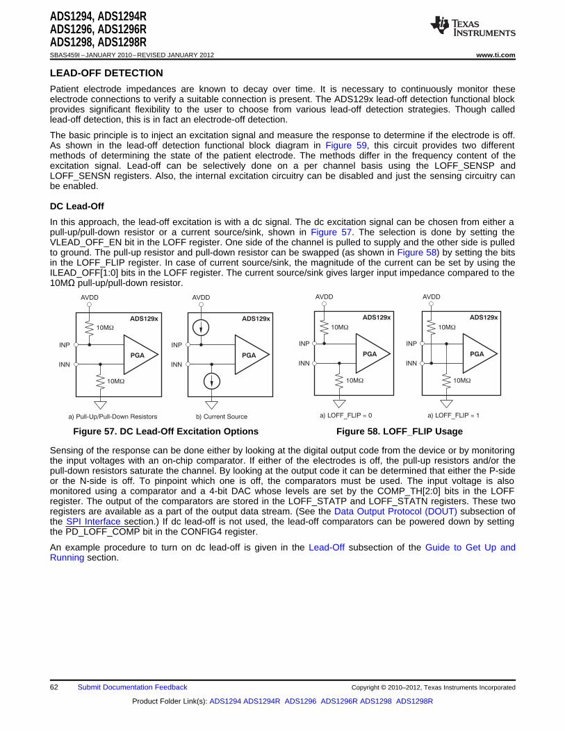
a) LOFF_FLIP = 0 a) LOFF_FLIP = 1
PGA
10MW
10MW
AVDD
INP
INN
PGA
10MW
10MW
AVDD
INP
INN
ADS129x ADS129x
a) Pull-Up/Pull-Down Resistors b) Current Source
PGA
10MW
10MW
AVDD
INP
INN
PGA
AVDD
INP
INN
ADS129xADS129x
ADS1294, ADS1294RADS1296, ADS1296RADS1298, ADS1298RSBAS459I –JANUARY 2010–REVISED JANUARY 2012 www.ti.com
LEAD-OFF DETECTION
Patient electrode impedances are known to decay over time. It is necessary to continuously monitor theseelectrode connections to verify a suitable connection is present. The ADS129x lead-off detection functional blockprovides significant flexibility to the user to choose from various lead-off detection strategies. Though calledlead-off detection, this is in fact an electrode-off detection.
The basic principle is to inject an excitation signal and measure the response to determine if the electrode is off.As shown in the lead-off detection functional block diagram in Figure 59, this circuit provides two differentmethods of determining the state of the patient electrode. The methods differ in the frequency content of theexcitation signal. Lead-off can be selectively done on a per channel basis using the LOFF_SENSP andLOFF_SENSN registers. Also, the internal excitation circuitry can be disabled and just the sensing circuitry canbe enabled.
DC Lead-Off
In this approach, the lead-off excitation is with a dc signal. The dc excitation signal can be chosen from either apull-up/pull-down resistor or a current source/sink, shown in Figure 57. The selection is done by setting theVLEAD_OFF_EN bit in the LOFF register. One side of the channel is pulled to supply and the other side is pulledto ground. The pull-up resistor and pull-down resistor can be swapped (as shown in Figure 58) by setting the bitsin the LOFF_FLIP register. In case of current source/sink, the magnitude of the current can be set by using theILEAD_OFF[1:0] bits in the LOFF register. The current source/sink gives larger input impedance compared to the10MΩ pull-up/pull-down resistor.
Figure 57. DC Lead-Off Excitation Options Figure 58. LOFF_FLIP Usage
Sensing of the response can be done either by looking at the digital output code from the device or by monitoringthe input voltages with an on-chip comparator. If either of the electrodes is off, the pull-up resistors and/or thepull-down resistors saturate the channel. By looking at the output code it can be determined that either the P-sideor the N-side is off. To pinpoint which one is off, the comparators must be used. The input voltage is alsomonitored using a comparator and a 4-bit DAC whose levels are set by the COMP_TH[2:0] bits in the LOFFregister. The output of the comparators are stored in the LOFF_STATP and LOFF_STATN registers. These tworegisters are available as a part of the output data stream. (See the Data Output Protocol (DOUT) subsection ofthe SPI Interface section.) If dc lead-off is not used, the lead-off comparators can be powered down by settingthe PD_LOFF_COMP bit in the CONFIG4 register.
An example procedure to turn on dc lead-off is given in the Lead-Off subsection of the Guide to Get Up andRunning section.
62 Submit Documentation Feedback Copyright © 2010–2012, Texas Instruments Incorporated
Product Folder Link(s): ADS1294 ADS1294R ADS1296 ADS1296R ADS1298 ADS1298R
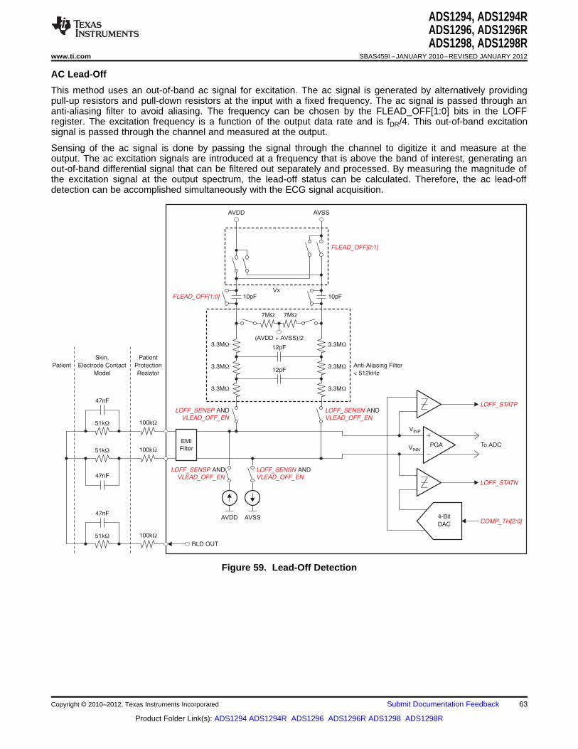
51kW
51kW
100kW
100kW
47nF
51kW100kW
47nF
47nF
4-Bit
DAC
Skin,
Electrode Contact
Model
Patient
Protection
Resistor
AVDD
LOFF_SENSP
VLEAD_OFF_EN
AND
AVSS
LOFF_SENSN
VLEAD_OFF_EN
AND
LOFF_SENSP
VLEAD_OFF_EN
AND LOFF_SENSN
VLEAD_OFF_EN
AND
RLD OUT
FLEAD_OFF[1:0]Vx
3.3MW
3.3MW
3.3MW
3.3MW
3.3MW
3.3MW
Anti-Aliasing Filter
< 512kHz
FLEAD_OFF[0:1]
AVDD AVSS
To ADC
LOFF_STATP
LOFF_STATN
COMP_TH[2:0]
VINP
VINN
(AVDD + AVSS)/2
7MW 7MW
10pF 10pF
PGAEMI
Filter
12pF
12pFPatient
ADS1294, ADS1294RADS1296, ADS1296RADS1298, ADS1298R
www.ti.com SBAS459I –JANUARY 2010–REVISED JANUARY 2012
AC Lead-Off
This method uses an out-of-band ac signal for excitation. The ac signal is generated by alternatively providingpull-up resistors and pull-down resistors at the input with a fixed frequency. The ac signal is passed through ananti-aliasing filter to avoid aliasing. The frequency can be chosen by the FLEAD_OFF[1:0] bits in the LOFFregister. The excitation frequency is a function of the output data rate and is fDR/4. This out-of-band excitationsignal is passed through the channel and measured at the output.
Sensing of the ac signal is done by passing the signal through the channel to digitize it and measure at theoutput. The ac excitation signals are introduced at a frequency that is above the band of interest, generating anout-of-band differential signal that can be filtered out separately and processed. By measuring the magnitude ofthe excitation signal at the output spectrum, the lead-off status can be calculated. Therefore, the ac lead-offdetection can be accomplished simultaneously with the ECG signal acquisition.
Figure 59. Lead-Off Detection
Copyright © 2010–2012, Texas Instruments Incorporated Submit Documentation Feedback 63
Product Folder Link(s): ADS1294 ADS1294R ADS1296 ADS1296R ADS1298 ADS1298R
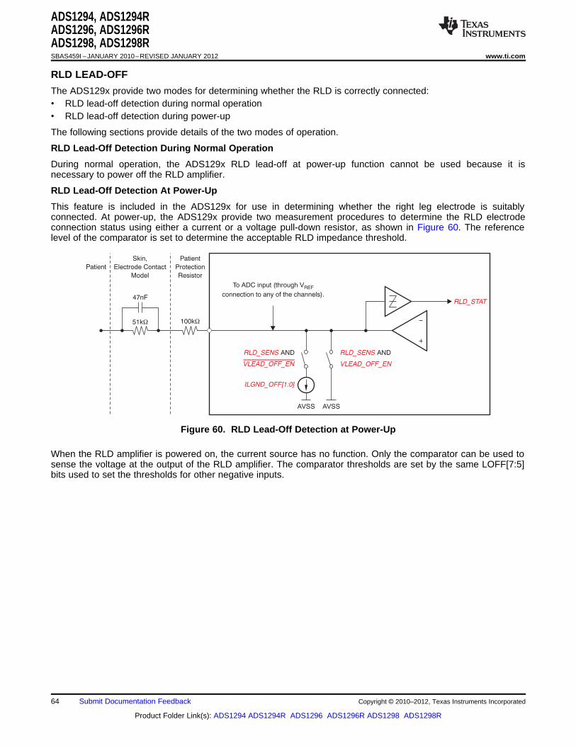
51kW100kW
47nF
Skin,
Electrode Contact
Model
Patient
Protection
Resistor
AVSS
RLD_SENS
VLEAD_OFF_EN
AND
AVSS
RLD_STAT
Patient
RLD_SENS
VLEAD_OFF_EN
AND
To ADC input (through V
connection to any of the channels).REF
ILGND_OFF[1:0]
ADS1294, ADS1294RADS1296, ADS1296RADS1298, ADS1298RSBAS459I –JANUARY 2010–REVISED JANUARY 2012 www.ti.com
RLD LEAD-OFF
The ADS129x provide two modes for determining whether the RLD is correctly connected:• RLD lead-off detection during normal operation• RLD lead-off detection during power-up
The following sections provide details of the two modes of operation.
RLD Lead-Off Detection During Normal Operation
During normal operation, the ADS129x RLD lead-off at power-up function cannot be used because it isnecessary to power off the RLD amplifier.
RLD Lead-Off Detection At Power-Up
This feature is included in the ADS129x for use in determining whether the right leg electrode is suitablyconnected. At power-up, the ADS129x provide two measurement procedures to determine the RLD electrodeconnection status using either a current or a voltage pull-down resistor, as shown in Figure 60. The referencelevel of the comparator is set to determine the acceptable RLD impedance threshold.
Figure 60. RLD Lead-Off Detection at Power-Up
When the RLD amplifier is powered on, the current source has no function. Only the comparator can be used tosense the voltage at the output of the RLD amplifier. The comparator thresholds are set by the same LOFF[7:5]bits used to set the thresholds for other negative inputs.
64 Submit Documentation Feedback Copyright © 2010–2012, Texas Instruments Incorporated
Product Folder Link(s): ADS1294 ADS1294R ADS1296 ADS1296R ADS1298 ADS1298R
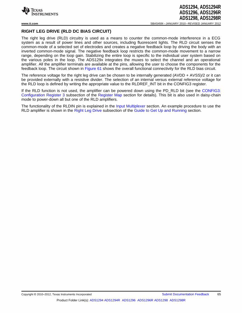
ADS1294, ADS1294RADS1296, ADS1296RADS1298, ADS1298R
www.ti.com SBAS459I –JANUARY 2010–REVISED JANUARY 2012
RIGHT LEG DRIVE (RLD DC BIAS CIRCUIT)
The right leg drive (RLD) circuitry is used as a means to counter the common-mode interference in a ECGsystem as a result of power lines and other sources, including fluorescent lights. The RLD circuit senses thecommon-mode of a selected set of electrodes and creates a negative feedback loop by driving the body with aninverted common-mode signal. The negative feedback loop restricts the common-mode movement to a narrowrange, depending on the loop gain. Stabilizing the entire loop is specific to the individual user system based onthe various poles in the loop. The ADS129x integrates the muxes to select the channel and an operationalamplifier. All the amplifier terminals are available at the pins, allowing the user to choose the components for thefeedback loop. The circuit shown in Figure 61 shows the overall functional connectivity for the RLD bias circuit.
The reference voltage for the right leg drive can be chosen to be internally generated (AVDD + AVSS)/2 or it canbe provided externally with a resistive divider. The selection of an internal versus external reference voltage forthe RLD loop is defined by writing the appropriate value to the RLDREF_INT bit in the CONFIG3 register.
If the RLD function is not used, the amplifier can be powered down using the PD_RLD bit (see the CONFIG3:Configuration Register 3 subsection of the Register Map section for details). This bit is also used in daisy-chainmode to power-down all but one of the RLD amplifiers.
The functionality of the RLDIN pin is explained in the Input Multiplexer section. An example procedure to use theRLD amplifier is shown in the Right Leg Drive subsection of the Guide to Get Up and Running section.
Copyright © 2010–2012, Texas Instruments Incorporated Submit Documentation Feedback 65
Product Folder Link(s): ADS1294 ADS1294R ADS1296 ADS1296R ADS1298 ADS1298R
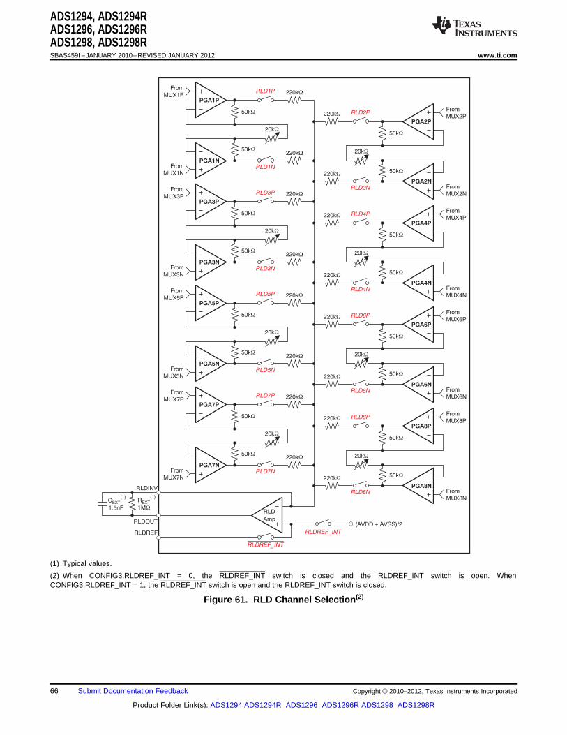
220kW
50kW
50kW
RLD1P
220kW
20kW
RLD1N
220kW
50kW
50kW
RLD2P
20kW
220kW
RLD2N
From
MUX1P
From
MUX2P
From
MUX2N
From
MUX1N
220kW
50kW
50kW
RLD3P
220kW
20kW
RLD3N
220kW
50kW
50kW
RLD4P
20kW
220kW
RLD4N
From
MUX3P
From
MUX4P
From
MUX4N
From
MUX3N
220kW
50kW
50kW
RLD5P
220kW
20kW
RLD5N
220kW
50kW
50kW
RLD6P
20kW
220kW
RLD6N
From
MUX5P
From
MUX6P
From
MUX6N
(AVDD + AVSS)/2RLDOUT
From
MUX5N
220kW
50kW
50kW
R(1)
EXT
1MW
C(1)
EXT
1.5nF
RLD7P
220kW
20kW
RLD7N
220kW
50kW
50kW
RLD8P
20kW
220kW
RLD8N
RLDREF_INT
From
MUX7P
From
MUX8P
From
MUX8N
From
MUX7N
RLD
Amp
RLDINV
RLDREF
RLDREF_INT
PGA1P
PGA1N
PGA3P
PGA3N
PGA5P
PGA5N
PGA7P
PGA7N
PGA8N
PGA8P
PGA6N
PGA6P
PGA4N
PGA4P
PGA2N
PGA2P
ADS1294, ADS1294RADS1296, ADS1296RADS1298, ADS1298RSBAS459I –JANUARY 2010–REVISED JANUARY 2012 www.ti.com
(1) Typical values.
(2) When CONFIG3.RLDREF_INT = 0, the RLDREF_INT switch is closed and the RLDREF_INT switch is open. WhenCONFIG3.RLDREF_INT = 1, the RLDREF_INT switch is open and the RLDREF_INT switch is closed.
Figure 61. RLD Channel Selection(2)
66 Submit Documentation Feedback Copyright © 2010–2012, Texas Instruments Incorporated
Product Folder Link(s): ADS1294 ADS1294R ADS1296 ADS1296R ADS1298 ADS1298R
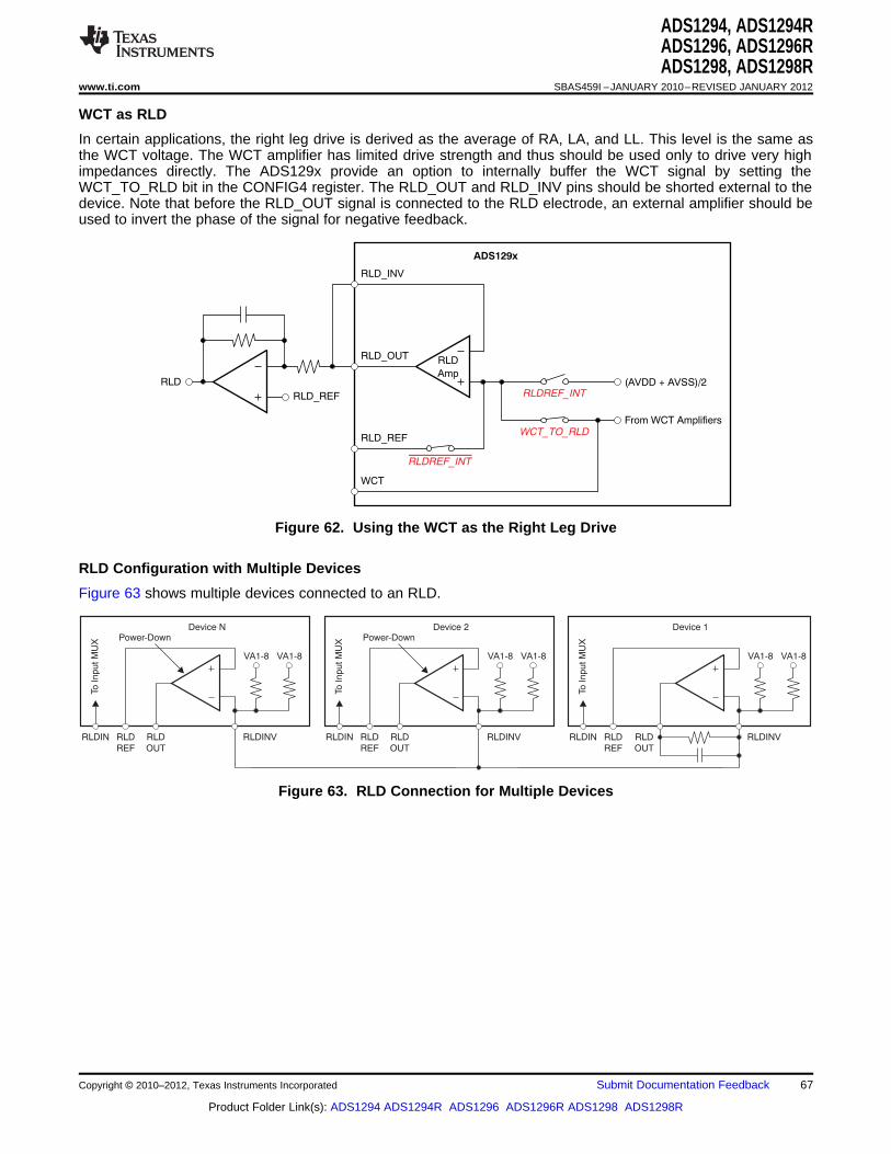
RLD
Amp(AVDD + AVSS)/2
RLDREF_INT
RLDREF_INT
RLD_REF
RLD_OUT
RLD_INV
RLD
ADS129x
WCT_TO_RLDFrom WCT Amplifiers
RLD_REF
WCT
RLDINVRLD
OUT
RLD
REF
RLDIN
VA1-8
Device 2
VA1-8
RLDINVRLD
OUT
RLD
REF
RLDIN
VA1-8
Device N
VA1-8
Power-Down Power-Down
RLDINVRLD
OUT
RLD
REF
RLDIN
VA1-8
Device 1
VA1-8
To I
np
ut
MU
X
To I
np
ut
MU
X
To I
np
ut
MU
X
ADS1294, ADS1294RADS1296, ADS1296RADS1298, ADS1298R
www.ti.com SBAS459I –JANUARY 2010–REVISED JANUARY 2012
WCT as RLD
In certain applications, the right leg drive is derived as the average of RA, LA, and LL. This level is the same asthe WCT voltage. The WCT amplifier has limited drive strength and thus should be used only to drive very highimpedances directly. The ADS129x provide an option to internally buffer the WCT signal by setting theWCT_TO_RLD bit in the CONFIG4 register. The RLD_OUT and RLD_INV pins should be shorted external to thedevice. Note that before the RLD_OUT signal is connected to the RLD electrode, an external amplifier should beused to invert the phase of the signal for negative feedback.
Figure 62. Using the WCT as the Right Leg Drive
RLD Configuration with Multiple Devices
Figure 63 shows multiple devices connected to an RLD.
Figure 63. RLD Connection for Multiple Devices
Copyright © 2010–2012, Texas Instruments Incorporated Submit Documentation Feedback 67
Product Folder Link(s): ADS1294 ADS1294R ADS1296 ADS1296R ADS1298 ADS1298R
ADS1294, ADS1294RADS1296, ADS1296RADS1298, ADS1298RSBAS459I –JANUARY 2010–REVISED JANUARY 2012 www.ti.com
PACE DETECT
The ADS129x provide flexibility for PACE detection either in software or by external hardware. The softwareapproach is made possible by providing sampling rates up to 32kSPS. The external hardware approach is madepossible by bringing out the output of the PGA at two pins: TESTP_PACE_OUT1 and TESTN_PACE_OUT2.Note that if the WCT amplifier is connected to the signal path, the user sees switching noise as a result ofchopping; see the Wilson Central Terminal (WCT) section for details.
Software Approach
To use the software approach, the device must be operated at 8kSPS or more to be able to capture the fastestpulse. Afterwards, digital signal processing can be used to identify the presence of the pacemaker pulse. Thesoftware approach gives the utmost flexibility to the user to be able to program the PACE detect threshold on thefly using software. This becomes increasingly important as pacemakers evolve over time. Two parameters mustbe considered while measuring fast PACE pulses:1. The PGA bandwidth shown in Table 6.2. For a step change in input, the digital decimation filter takes 3 × tDR to settle. The PGA bandwidth determines
the gain setting that can be used and the settling time determines the data rate that the device must beoperated at.
External Hardware Approach
One of the drawbacks of using the software approach is that all channels on a single device must operate athigher data rates. For systems where it is of concern, the ADS129x provide the option of bringing out the outputof the PGA. External hardware circuitry can be used to detect the presence of the pulse. The output of the PACEdetection logic can then be fed into the device through one of the GPIO pins. The GPIO data are transmittedthrough the SPI port and loaded 2tCLKs before DRDY goes low. Two of the eight channels can be selected usingregister bits in the PACE register, one from the odd-numbered channels and the other from the even-numberedchannels. During the differential to single-ended conversion, there is an attenuation of 0.4. Therefore, the totalgain in the PACE path is equal to (0.4 × PGA_GAIN). The PACE out signals are multiplexed with the TESTP andTESTN signals through the TESTP_PACE_OUT1 and TESTN_PACE_OUT2 pins respectively. The channelselection is done by setting bits[4:1] of the PACE register. If the PACE circuitry is not used, the PACE amplifierscan be turned off using the PD_PACE bit in the PACE register.
Note that if the output of a channel connected to the WCT amplifier (for example, the V lead channels) isconnected to one of the PACE amplifiers for external PACE detection, the artifact of chopping appears at thePACE amplifier output. Refer to the Wilson Central Terminal (WCT) section for more details.
68 Submit Documentation Feedback Copyright © 2010–2012, Texas Instruments Incorporated
Product Folder Link(s): ADS1294 ADS1294R ADS1296 ADS1296R ADS1298 ADS1298R
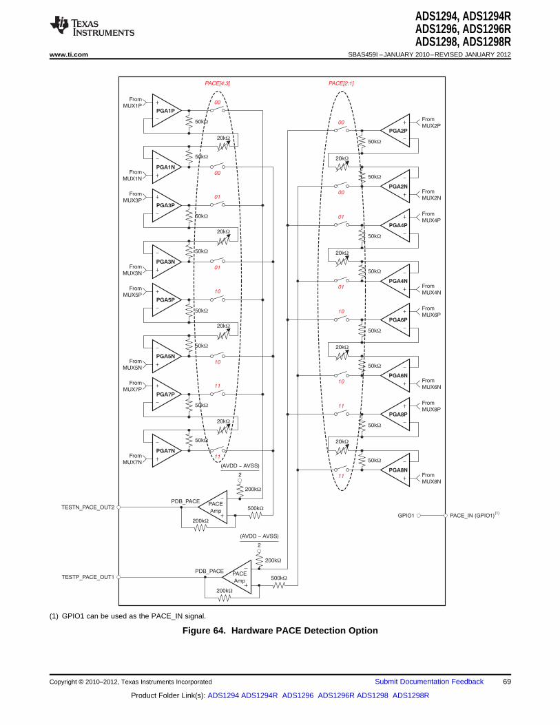
50kW
50kW
00
PACE[4:3]
20kW
00
50kW
50kW
00
PACE[2:1]
00
From
MUX1P
From
MUX2P
From
MUX2N
From
MUX1N
50kW
50kW
01
01
50kW
50kW
01
01
From
MUX3P
From
MUX4P
From
MUX4N
From
MUX3N
50kW
50kW
10
10
50kW
50kW
10
10
From
MUX5P
From
MUX6P
From
MUX6N
PACE_IN (GPIO1)(1)
GPIO1
From
MUX5N
50kW
50kW
200kW
11
200kW
11
50kW
50kW
11
11
From
MUX7P
From
MUX8P
From
MUX8N
From
MUX7N
TESTN_PACE_OUT2PACE
Amp
PDB_PACE
200kW
200kW
TESTP_PACE_OUT1PACE
Amp
PDB_PACE
20kW
20kW
20kW
20kW
20kW
20kW
20kW
PGA1P
PGA2P
PGA1N
PGA3P
PGA7N
PGA7P
PGA5N
PGA5P
PGA3N
PGA2N
PGA4P
PGA4N
PGA6P
PGA6N
PGA8P
PGA8N-(AVDD AVSS)
2
-(AVDD AVSS)
2
500kW
500kW
ADS1294, ADS1294RADS1296, ADS1296RADS1298, ADS1298R
www.ti.com SBAS459I –JANUARY 2010–REVISED JANUARY 2012
(1) GPIO1 can be used as the PACE_IN signal.
Figure 64. Hardware PACE Detection Option
Copyright © 2010–2012, Texas Instruments Incorporated Submit Documentation Feedback 69
Product Folder Link(s): ADS1294 ADS1294R ADS1296 ADS1296R ADS1298 ADS1298R
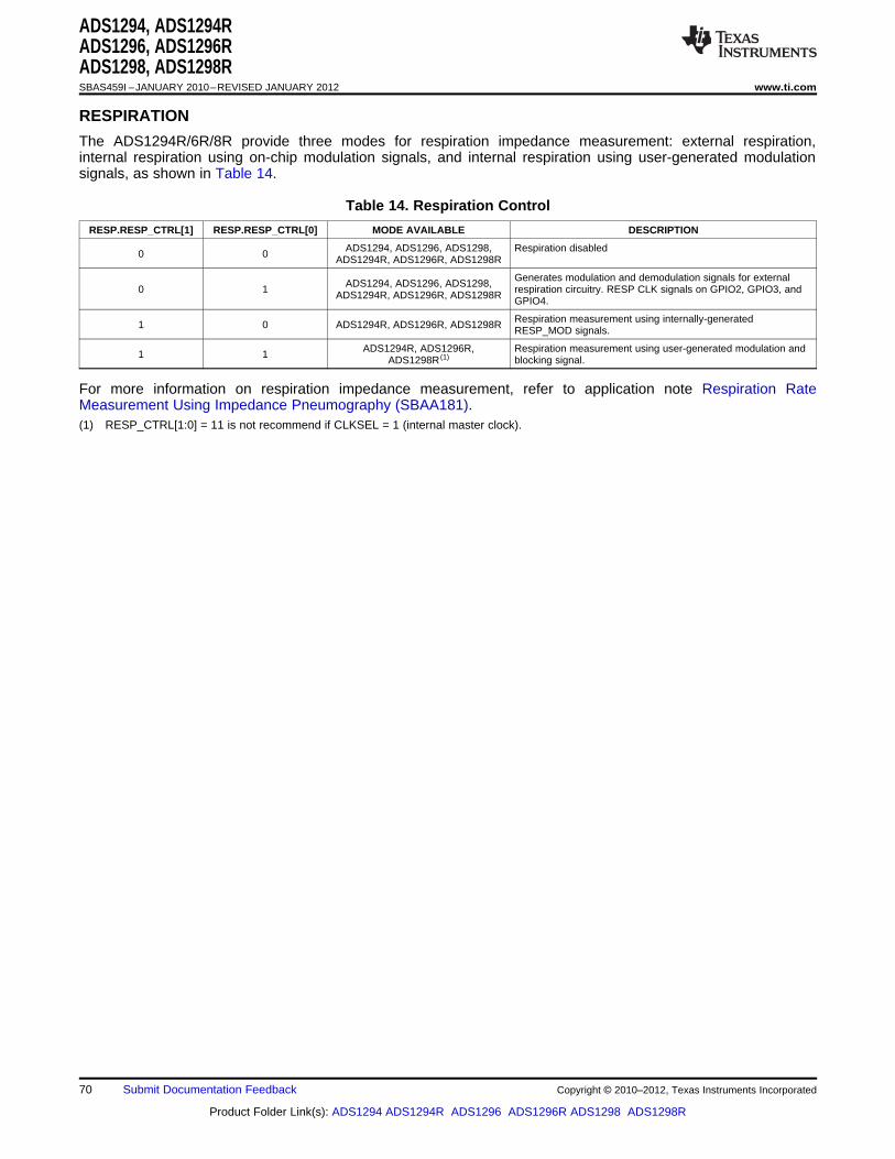
ADS1294, ADS1294RADS1296, ADS1296RADS1298, ADS1298RSBAS459I –JANUARY 2010–REVISED JANUARY 2012 www.ti.com
RESPIRATION
The ADS1294R/6R/8R provide three modes for respiration impedance measurement: external respiration,internal respiration using on-chip modulation signals, and internal respiration using user-generated modulationsignals, as shown in Table 14.
Table 14. Respiration Control
RESP.RESP_CTRL[1] RESP.RESP_CTRL[0] MODE AVAILABLE DESCRIPTION
ADS1294, ADS1296, ADS1298, Respiration disabled0 0 ADS1294R, ADS1296R, ADS1298R
Generates modulation and demodulation signals for externalADS1294, ADS1296, ADS1298,0 1 respiration circuitry. RESP CLK signals on GPIO2, GPIO3, andADS1294R, ADS1296R, ADS1298R GPIO4.
Respiration measurement using internally-generated1 0 ADS1294R, ADS1296R, ADS1298R RESP_MOD signals.
ADS1294R, ADS1296R, Respiration measurement using user-generated modulation and1 1 ADS1298R (1) blocking signal.
For more information on respiration impedance measurement, refer to application note Respiration RateMeasurement Using Impedance Pneumography (SBAA181).(1) RESP_CTRL[1:0] = 11 is not recommend if CLKSEL = 1 (internal master clock).
70 Submit Documentation Feedback Copyright © 2010–2012, Texas Instruments Incorporated
Product Folder Link(s): ADS1294 ADS1294R ADS1296 ADS1296R ADS1298 ADS1298R
GPIO3
GPIO4
GPIO2
tBLKDLY
(Demodulation Clock)
(Blocki gn Si n l)g a
tPHASE
(Modulation Cl ck)o
Respiration
Modulation
Generator
RESP_PH[2:0]
CLK
(2.048MHz)
Modulation Clock
Demodulation Clock
GPIO4
GPIO3
GPIO2
ADS1294, ADS1294RADS1296, ADS1296RADS1298, ADS1298R
www.ti.com SBAS459I –JANUARY 2010–REVISED JANUARY 2012
External Respiration Circuitry Option (RESP_CTRL = 01b)
In this mode, GPIO2, GPIO3, and GPIO4 are automatically configured as outputs. The phase relationshipbetween the signals is shown in Figure 65. GPIO2 is the exclusive-OR of GPIO3 and GPIO4, as shown inFigure 66. GPIO3 is the modulation signal, and GPIO4 is the de-modulation signal. While in this mode, thegeneral-purpose pin function of GPIO2, GPIO3, and GPIO4 is not available. The modulation frequency can be64kHz or 32kHz using RESP_FREQ[2:0] bits in the CONFIG4 register. The remaining bit options ofRESP_FREQ[2:0] generate square waves on GPIO3 and GPIO4. The exclusive-OR out on GPIO2 is onlyavailable on 64kHz and 32kHz modes. The phase of GPIO4, relative to GPIO3, is set by RESP_PH[2:0] bits inthe RESP register.
The mode can be used when the user implements custom respiration impedance circuitry external to theADS129x.
Figure 65. External Respiration (RESP_CTRL = 01b) Timing Diagram
Table 15. Timing Characteristics for Figure 65(1)
2.7V ≤ DVDD ≤ 3.6V 1.65V ≤ DVDD ≤ 2VPARAMETER DESCRIPTION MIN TYP MAX MIN TYP MAX UNIT
Respiration phase delay, set bytPHASE 22.5 157.5 22.5 157.5 DegreesRESP.RESP_PH[2:0] bits
Modulation clock rising edge to XORtBLKDLY 1 5 nssignal
(1) Specifications apply from –40°C to +85°C.
Figure 66. External Respiration (RESP_CTRL = 01b) Block Diagram
Copyright © 2010–2012, Texas Instruments Incorporated Submit Documentation Feedback 71
Product Folder Link(s): ADS1294 ADS1294R ADS1296 ADS1296R ADS1298 ADS1298R
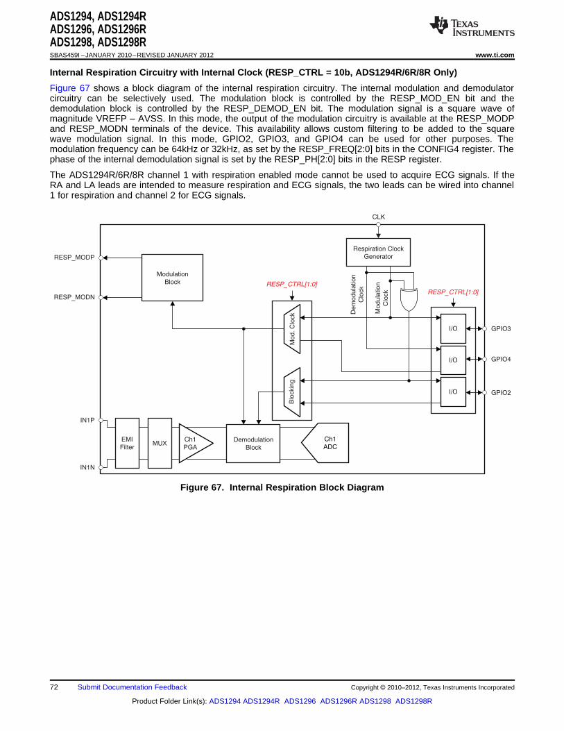
Ch1
ADC
Modulation
Block
Demodulation
Block
RESP_CTRL[1:0]
Ch1
PGA
Respiration Clock
Generator
CLK
I/O
I/O
I/O
RESP_CTRL[1:0]
GPIO3
GPIO4
GPIO2
RESP_MODP
RESP_MODN
IN1P
IN1N
EMI
FilterMUX
Blo
ckin
g
Dem
odula
tion
Clo
ck
Modula
tion
Clo
ck
Mod. C
lock
ADS1294, ADS1294RADS1296, ADS1296RADS1298, ADS1298RSBAS459I –JANUARY 2010–REVISED JANUARY 2012 www.ti.com
Internal Respiration Circuitry with Internal Clock (RESP_CTRL = 10b, ADS1294R/6R/8R Only)
Figure 67 shows a block diagram of the internal respiration circuitry. The internal modulation and demodulatorcircuitry can be selectively used. The modulation block is controlled by the RESP_MOD_EN bit and thedemodulation block is controlled by the RESP_DEMOD_EN bit. The modulation signal is a square wave ofmagnitude VREFP – AVSS. In this mode, the output of the modulation circuitry is available at the RESP_MODPand RESP_MODN terminals of the device. This availability allows custom filtering to be added to the squarewave modulation signal. In this mode, GPIO2, GPIO3, and GPIO4 can be used for other purposes. Themodulation frequency can be 64kHz or 32kHz, as set by the RESP_FREQ[2:0] bits in the CONFIG4 register. Thephase of the internal demodulation signal is set by the RESP_PH[2:0] bits in the RESP register.
The ADS1294R/6R/8R channel 1 with respiration enabled mode cannot be used to acquire ECG signals. If theRA and LA leads are intended to measure respiration and ECG signals, the two leads can be wired into channel1 for respiration and channel 2 for ECG signals.
Figure 67. Internal Respiration Block Diagram
72 Submit Documentation Feedback Copyright © 2010–2012, Texas Instruments Incorporated
Product Folder Link(s): ADS1294 ADS1294R ADS1296 ADS1296R ADS1298 ADS1298R
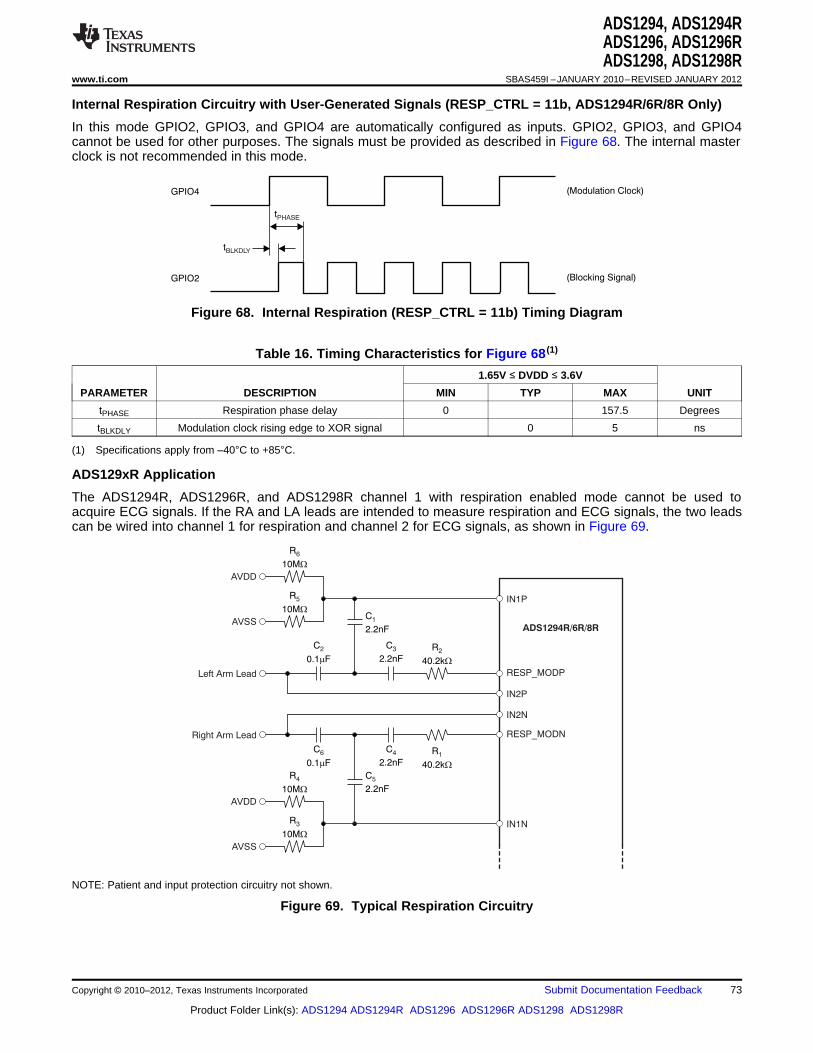
GPIO4
GPIO2
tBLKDLY
(Blocki gn Si n l)g a
tPHASE
(Modulation Cl ck)o
R
10MW
6
R
10MW
5
C
2.2nF1
R
40.2kW
2C
0.1 Fm
2 C
2.2nF3
AVDD
AVSS
Left Arm Lead RESP_MODP
IN1P
IN2P
Right Arm Lead RESP_MODN
IN2N
R
40.2kW
1C
0.1 Fm
6 C
2.2nF4
C
2.2nF5R
10MW
4
R
10MW
3
AVDD
AVSS
IN1N
ADS1294R/6R/8R
ADS1294, ADS1294RADS1296, ADS1296RADS1298, ADS1298R
www.ti.com SBAS459I –JANUARY 2010–REVISED JANUARY 2012
Internal Respiration Circuitry with User-Generated Signals (RESP_CTRL = 11b, ADS1294R/6R/8R Only)
In this mode GPIO2, GPIO3, and GPIO4 are automatically configured as inputs. GPIO2, GPIO3, and GPIO4cannot be used for other purposes. The signals must be provided as described in Figure 68. The internal masterclock is not recommended in this mode.
Figure 68. Internal Respiration (RESP_CTRL = 11b) Timing Diagram
Table 16. Timing Characteristics for Figure 68(1)
1.65V ≤ DVDD ≤ 3.6V
PARAMETER DESCRIPTION MIN TYP MAX UNIT
tPHASE Respiration phase delay 0 157.5 Degrees
tBLKDLY Modulation clock rising edge to XOR signal 0 5 ns
(1) Specifications apply from –40°C to +85°C.
ADS129xR Application
The ADS1294R, ADS1296R, and ADS1298R channel 1 with respiration enabled mode cannot be used toacquire ECG signals. If the RA and LA leads are intended to measure respiration and ECG signals, the two leadscan be wired into channel 1 for respiration and channel 2 for ECG signals, as shown in Figure 69.
NOTE: Patient and input protection circuitry not shown.
Figure 69. Typical Respiration Circuitry
Copyright © 2010–2012, Texas Instruments Incorporated Submit Documentation Feedback 73
Product Folder Link(s): ADS1294 ADS1294R ADS1296 ADS1296R ADS1298 ADS1298R
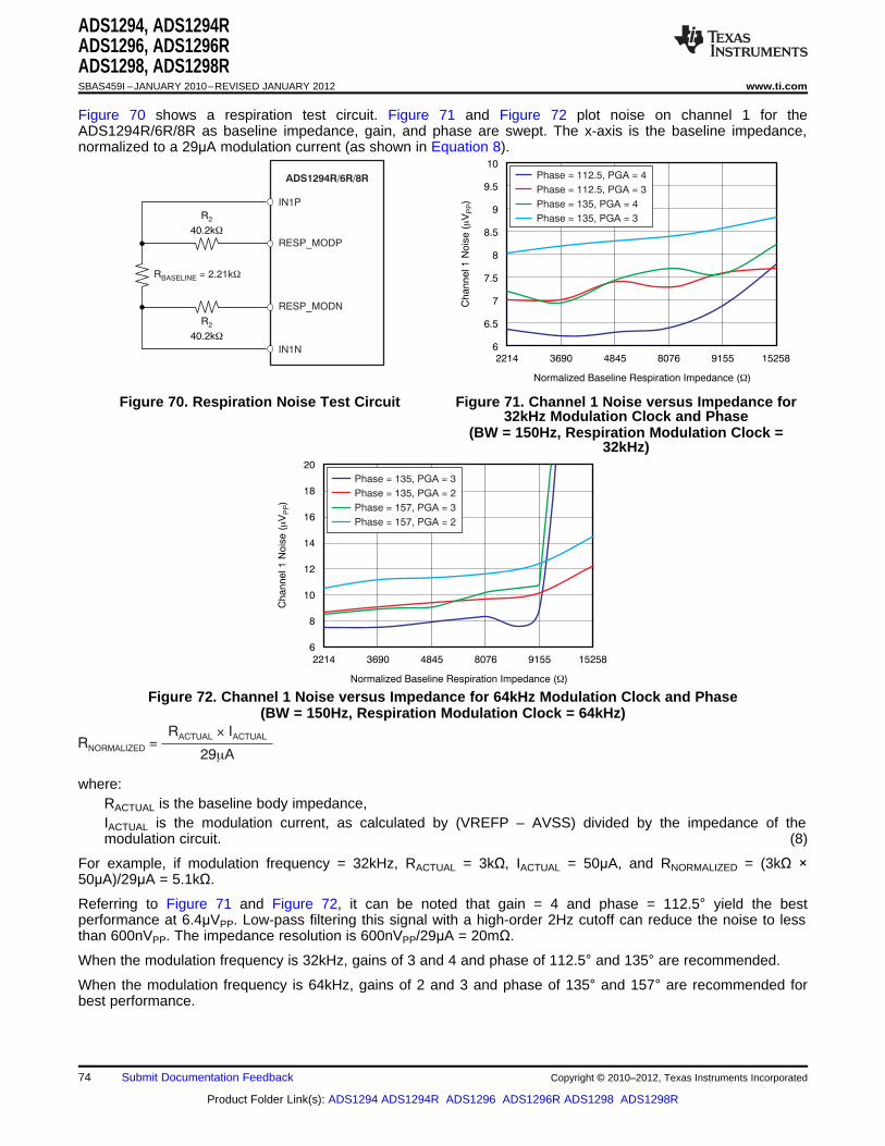
R
40.2kW
2
R = 2.21kWBASELINE
R
40.2kW
2
IN1P
RESP_MODP
RESP_MODN
IN1N
ADS1294R/6R/8R
10
9.5
9
8.5
8
7.5
7
6.5
6
Normalized Baseline Respiration Impedance ( )W
Channel 1 N
ois
e (
V)
mP
P
3690 48452214 152588076 9155
Phase = 112.5, PGA = 4
Phase = 112.5, PGA = 3
Phase = 135, PGA = 4
Phase = 135, PGA = 3
20
18
16
14
12
10
8
6
Normalized Baseline Respiration Impedance ( )W
Channel 1 N
ois
e (
V)
mP
P
3690 48452214 152588076 9155
Phase = 135, PGA = 3
Phase = 135, PGA = 2
Phase = 157, PGA = 3
Phase = 157, PGA = 2
R =NORMALIZED
R I´ACTUAL ACTUAL
29 Am
ADS1294, ADS1294RADS1296, ADS1296RADS1298, ADS1298RSBAS459I –JANUARY 2010–REVISED JANUARY 2012 www.ti.com
Figure 70 shows a respiration test circuit. Figure 71 and Figure 72 plot noise on channel 1 for theADS1294R/6R/8R as baseline impedance, gain, and phase are swept. The x-axis is the baseline impedance,normalized to a 29µA modulation current (as shown in Equation 8).
Figure 70. Respiration Noise Test Circuit Figure 71. Channel 1 Noise versus Impedance for32kHz Modulation Clock and Phase
(BW = 150Hz, Respiration Modulation Clock =32kHz)
Figure 72. Channel 1 Noise versus Impedance for 64kHz Modulation Clock and Phase(BW = 150Hz, Respiration Modulation Clock = 64kHz)
where:RACTUAL is the baseline body impedance,IACTUAL is the modulation current, as calculated by (VREFP – AVSS) divided by the impedance of themodulation circuit. (8)
For example, if modulation frequency = 32kHz, RACTUAL = 3kΩ, IACTUAL = 50µA, and RNORMALIZED = (3kΩ ×50µA)/29µA = 5.1kΩ.
Referring to Figure 71 and Figure 72, it can be noted that gain = 4 and phase = 112.5° yield the bestperformance at 6.4µVPP. Low-pass filtering this signal with a high-order 2Hz cutoff can reduce the noise to lessthan 600nVPP. The impedance resolution is 600nVPP/29µA = 20mΩ.
When the modulation frequency is 32kHz, gains of 3 and 4 and phase of 112.5° and 135° are recommended.
When the modulation frequency is 64kHz, gains of 2 and 3 and phase of 135° and 157° are recommended forbest performance.
74 Submit Documentation Feedback Copyright © 2010–2012, Texas Instruments Incorporated
Product Folder Link(s): ADS1294 ADS1294R ADS1296 ADS1296R ADS1298 ADS1298R

ADS1298
AVDD
0.1 Fm1 Fm
+3V
AVDD1
AVSSAVSS1 DGND
DVDD
+1.8V
0.1 Fm 1 Fm
0.1 Fm
VREFP
VREFN
VCAP1
VCAP2
VCAP3
VCAP4
WCT
1nF 1 Fm 1 Fm 1 Fm
10 Fm
22 Fm0.1 Fm
RESV1
ADS1294, ADS1294RADS1296, ADS1296RADS1298, ADS1298R
www.ti.com SBAS459I –JANUARY 2010–REVISED JANUARY 2012
QUICK-START GUIDE
PCB LAYOUT
Power Supplies and Grounding
The ADS129x have three supplies: AVDD, AVDD1, and DVDD. Both AVDD and AVDD1 should be as quiet aspossible. AVDD1 provides the supply to the charge pump block and has transients at fCLK. Therefore, it isrecommended that AVDD1 and AVSS1 be star-connected to AVDD and AVSS. It is important to eliminate noisefrom AVDD and AVDD1 that is non-synchronous with the ADS129x operation. Each supply of the ADS129xshould be bypassed with 1μF and 0.1μF solid ceramic capacitors. It is recommended that placement of the digitalcircuits (DSP, microcontrollers, FPGAs, etc.) in the system is done such that the return currents on those devicesdo not cross the analog return path of the ADS129x. The ADS129x can be powered from unipolar or bipolarsupplies.
Capacitors used for decoupling can be of surface-mount, low-cost, low-profile, multi-layer ceramic type. In mostcases, the VCAP1 capacitor can also be a multi-layer ceramic, but in systems where the board is subjected tohigh- or low-frequency vibration, it is recommend to install a non-ferroelectric capacitor such as a tantalum orclass 1 capacitor (C0G or NPO). EIA class 2 and class 3 dielectrics such as (X7R, X5R, X8R, etc.) areferroelectric. The piezoelectric property of these capacitors can appear as electrical noise coming from thecapacitor. When using internal reference, noise on the VCAP1 node results in performance degradation.
Connecting the Device to Unipolar (+3V/+1.8V) Supplies
Figure 73 illustrates the ADS129x connected to a unipolar supply. In this example, analog supply (AVDD) isreferenced to analog ground (AVSS) and digital supplies (DVDD) are referenced to digital ground (DGND).
NOTE: Place the capacitors for supply, reference, WCT, and VCAP1 to VCAP4 as close to the package as possible.
Figure 73. Single-Supply Operation
Copyright © 2010–2012, Texas Instruments Incorporated Submit Documentation Feedback 75
Product Folder Link(s): ADS1294 ADS1294R ADS1296 ADS1296R ADS1298 ADS1298R
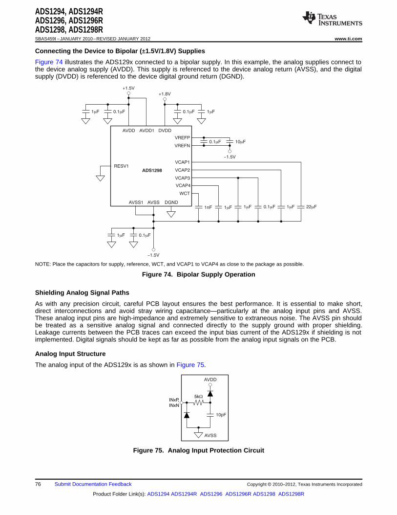
ADS1298
0.1 Fm1 Fm
AVDD AVDD1
0.1 Fm1 Fm
-1.5V
AVSSAVSS1 DGND
DVDD
+1.5V
+1.8V
0.1 Fm 1 Fm
VCAP1
VCAP2
VCAP3
0.1 Fm
VREFP
VREFN10 Fm
VCAP4
WCT
1 Fm 1 Fm1nF 1 Fm
-1.5V
22 Fm0.1 Fm
RESV1
5kW
10pF
AVSS
AVDD
INxP,
INxN
ADS1294, ADS1294RADS1296, ADS1296RADS1298, ADS1298RSBAS459I –JANUARY 2010–REVISED JANUARY 2012 www.ti.com
Connecting the Device to Bipolar (±1.5V/1.8V) Supplies
Figure 74 illustrates the ADS129x connected to a bipolar supply. In this example, the analog supplies connect tothe device analog supply (AVDD). This supply is referenced to the device analog return (AVSS), and the digitalsupply (DVDD) is referenced to the device digital ground return (DGND).
NOTE: Place the capacitors for supply, reference, WCT, and VCAP1 to VCAP4 as close to the package as possible.
Figure 74. Bipolar Supply Operation
Shielding Analog Signal Paths
As with any precision circuit, careful PCB layout ensures the best performance. It is essential to make short,direct interconnections and avoid stray wiring capacitance—particularly at the analog input pins and AVSS.These analog input pins are high-impedance and extremely sensitive to extraneous noise. The AVSS pin shouldbe treated as a sensitive analog signal and connected directly to the supply ground with proper shielding.Leakage currents between the PCB traces can exceed the input bias current of the ADS129x if shielding is notimplemented. Digital signals should be kept as far as possible from the analog input signals on the PCB.
Analog Input Structure
The analog input of the ADS129x is as shown in Figure 75.
Figure 75. Analog Input Protection Circuit
76 Submit Documentation Feedback Copyright © 2010–2012, Texas Instruments Incorporated
Product Folder Link(s): ADS1294 ADS1294R ADS1296 ADS1296R ADS1298 ADS1298R
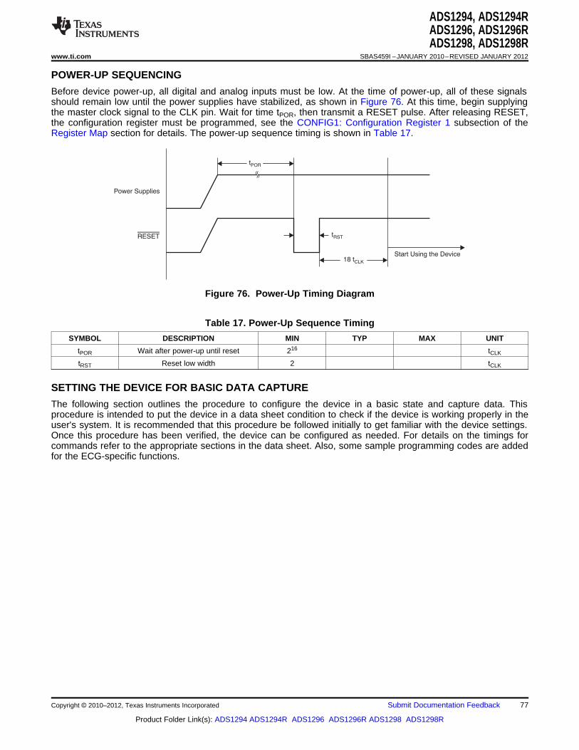
Power Supplies
RESET tRST
Start Using the Device
tPOR
18 tCLK
ADS1294, ADS1294RADS1296, ADS1296RADS1298, ADS1298R
www.ti.com SBAS459I –JANUARY 2010–REVISED JANUARY 2012
POWER-UP SEQUENCING
Before device power-up, all digital and analog inputs must be low. At the time of power-up, all of these signalsshould remain low until the power supplies have stabilized, as shown in Figure 76. At this time, begin supplyingthe master clock signal to the CLK pin. Wait for time tPOR, then transmit a RESET pulse. After releasing RESET,the configuration register must be programmed, see the CONFIG1: Configuration Register 1 subsection of theRegister Map section for details. The power-up sequence timing is shown in Table 17.
Figure 76. Power-Up Timing Diagram
Table 17. Power-Up Sequence Timing
SYMBOL DESCRIPTION MIN TYP MAX UNIT
tPOR Wait after power-up until reset 216 tCLK
tRST Reset low width 2 tCLK
SETTING THE DEVICE FOR BASIC DATA CAPTURE
The following section outlines the procedure to configure the device in a basic state and capture data. Thisprocedure is intended to put the device in a data sheet condition to check if the device is working properly in theuser's system. It is recommended that this procedure be followed initially to get familiar with the device settings.Once this procedure has been verified, the device can be configured as needed. For details on the timings forcommands refer to the appropriate sections in the data sheet. Also, some sample programming codes are addedfor the ECG-specific functions.
Copyright © 2010–2012, Texas Instruments Incorporated Submit Documentation Feedback 77
Product Folder Link(s): ADS1294 ADS1294R ADS1296 ADS1296R ADS1298 ADS1298R
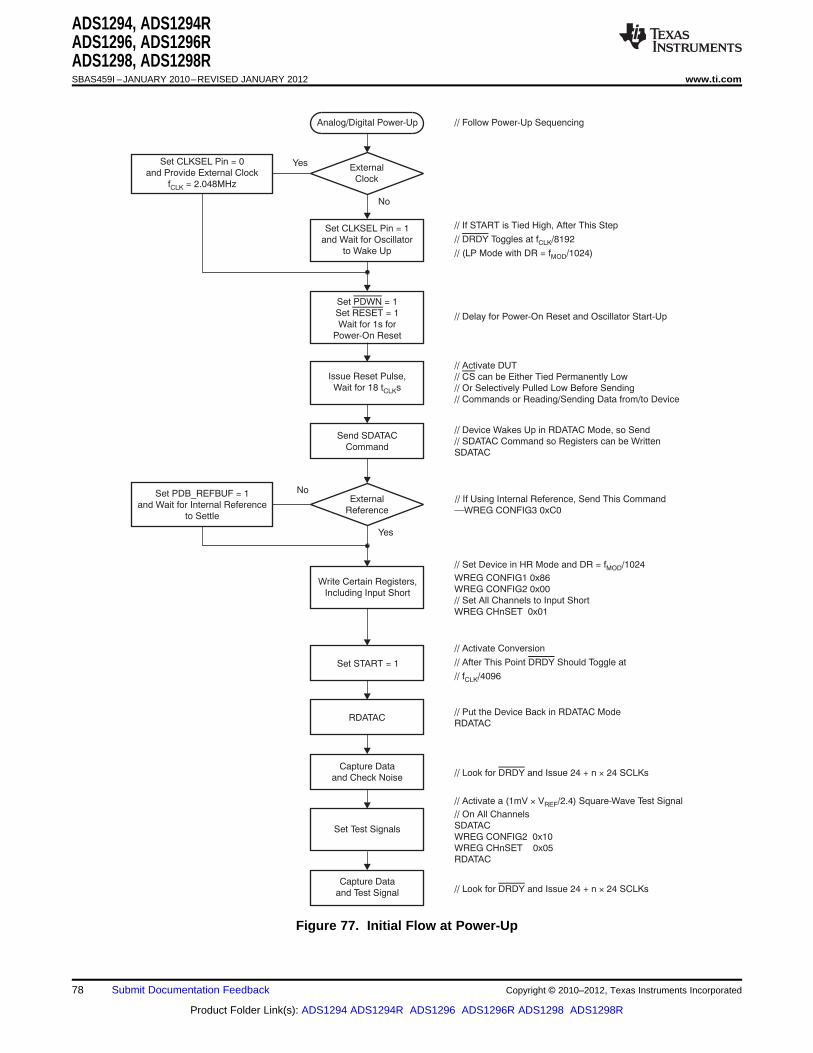
Set = 1
Set = 1
W it
PDWN
RESET
a fo 1sr f ro
Power-On Reset
// Delay for Power-On Reset and Oscillator art-UpSt
// If START is Tie Hi hd g , After This St pe
// Toggles at f /8192
// (LP Mode with DR = f /1024)
DRDY CLK
MOD
Set CLKSEL Pin = 1
and Wait for Oscillator
to Wake Up
No
Analog/Digital Po er-Upw // Follow Power-Up Sequencing
E ernaxt l
Clock
Set CLKSEL Pin = 0
and Provide External Clock
f = 2.048MHzCLK
Yes
Set PDB_R 1EFBUF =
and Wait for Internal Reference
to Settle
Write Certain Registers,
Including Input Short
Set START = 1
// Activate nversionCo
// After This Point Should Toggle at
// f /4096
DRDY
CLK
// Set Device in HR Mode and DR = f /1024
WREG CONFIG1 0x86
WREG CONFIG2 0x00
// Set All Channels to Input Short
WREG CHnSET 0x01
MOD
Yes
R ATACD// Put the Device Back in RDATAC Mode
RDATAC
Capture Data
and Check Noise// ookL for an Issu sdDRDY e 24 + n 24 SCLK´
Set Test Signals
Capture Data
and Test Signal
// ctivateA a 1mV V /2.´( 4) ve lSquare-Wa Test Signa
// On All Channels
SDATAC
WREG CONFIG2 0x10
WREG CHnSET 0x05
RDATAC
REF
// Look for a d Issu sDRDY n e 24 + n 24 SCLK´
External
Reference
// If Using Internal Reference, Send This Command
¾WREG CONFIG3 0xC0
No
Send SD TACA
Command
// Device Wakes Up in RDATAC Mode, so Send
// SDATAC Command so Registers can be Written
SDATAC
Issue Reset Pulse,
Wait for 18 t sCLK
// Activate DUT
// can be Either Tied Permanently Low
// Or Selectively Pulled Low Before Sending
// Commands or Reading/Sending Data from/to Device
CS
ADS1294, ADS1294RADS1296, ADS1296RADS1298, ADS1298RSBAS459I –JANUARY 2010–REVISED JANUARY 2012 www.ti.com
Figure 77. Initial Flow at Power-Up
78 Submit Documentation Feedback Copyright © 2010–2012, Texas Instruments Incorporated
Product Folder Link(s): ADS1294 ADS1294R ADS1296 ADS1296R ADS1298 ADS1298R
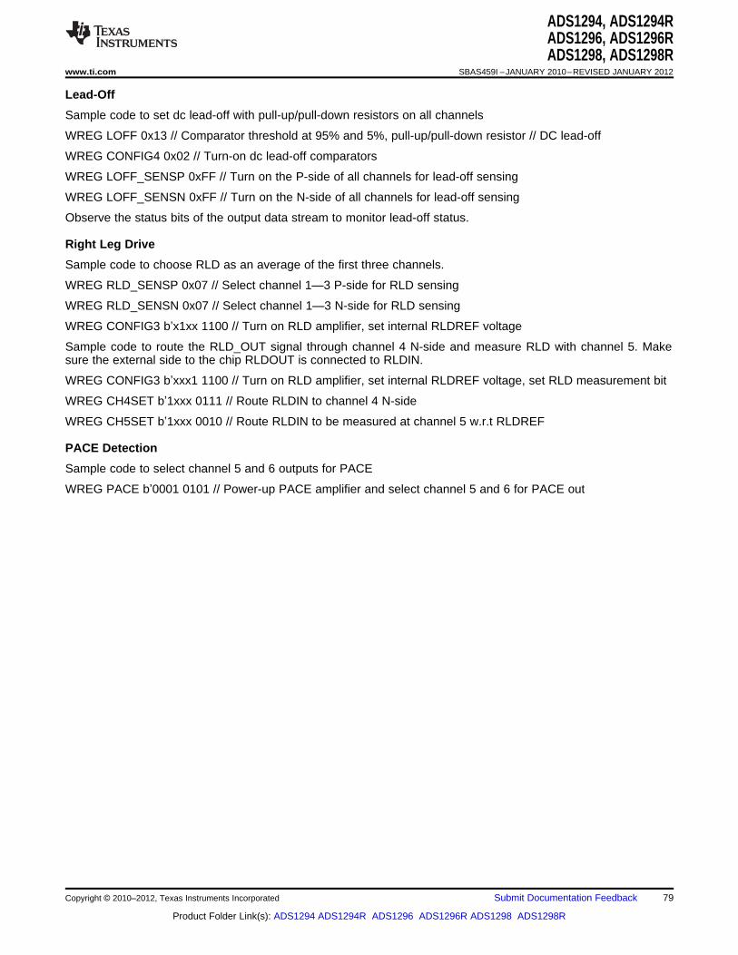
ADS1294, ADS1294RADS1296, ADS1296RADS1298, ADS1298R
www.ti.com SBAS459I –JANUARY 2010–REVISED JANUARY 2012
Lead-Off
Sample code to set dc lead-off with pull-up/pull-down resistors on all channels
WREG LOFF 0x13 // Comparator threshold at 95% and 5%, pull-up/pull-down resistor // DC lead-off
WREG CONFIG4 0x02 // Turn-on dc lead-off comparators
WREG LOFF_SENSP 0xFF // Turn on the P-side of all channels for lead-off sensing
WREG LOFF_SENSN 0xFF // Turn on the N-side of all channels for lead-off sensing
Observe the status bits of the output data stream to monitor lead-off status.
Right Leg Drive
Sample code to choose RLD as an average of the first three channels.
WREG RLD_SENSP 0x07 // Select channel 1—3 P-side for RLD sensing
WREG RLD_SENSN 0x07 // Select channel 1—3 N-side for RLD sensing
WREG CONFIG3 b’x1xx 1100 // Turn on RLD amplifier, set internal RLDREF voltage
Sample code to route the RLD_OUT signal through channel 4 N-side and measure RLD with channel 5. Makesure the external side to the chip RLDOUT is connected to RLDIN.
WREG CONFIG3 b’xxx1 1100 // Turn on RLD amplifier, set internal RLDREF voltage, set RLD measurement bit
WREG CH4SET b’1xxx 0111 // Route RLDIN to channel 4 N-side
WREG CH5SET b’1xxx 0010 // Route RLDIN to be measured at channel 5 w.r.t RLDREF
PACE Detection
Sample code to select channel 5 and 6 outputs for PACE
WREG PACE b’0001 0101 // Power-up PACE amplifier and select channel 5 and 6 for PACE out
Copyright © 2010–2012, Texas Instruments Incorporated Submit Documentation Feedback 79
Product Folder Link(s): ADS1294 ADS1294R ADS1296 ADS1296R ADS1298 ADS1298R

ADS1294, ADS1294RADS1296, ADS1296RADS1298, ADS1298RSBAS459I –JANUARY 2010–REVISED JANUARY 2012 www.ti.com
REVISION HISTORY
NOTE: Page numbers for previous revisions may differ from page numbers in the current version.
Changes from Revision H (October 2011) to Revision I Page
• Added eighth Features bullet (list of standards supported) .................................................................................................. 1
• Deleted duplicate Digital input voltage and Digital output voltage rows from Absolute Maximum Ratings table ................. 2
• Changed parameter name of Channel Performance, Common-mode rejection ratio and Power-supply rejection ratioparameters in Electrical Characteristics table ....................................................................................................................... 4
• Updated BGA pin out .......................................................................................................................................................... 10
• Updated Figure 23 .............................................................................................................................................................. 21
• Updated description of Analog Input section ...................................................................................................................... 24
• Updated Figure 29 .............................................................................................................................................................. 26
• Changed description of Data Ready (DRDY) section ......................................................................................................... 32
• Changed description of START pin in START section ....................................................................................................... 34
• Changed conversion description in Continuous Mode section ........................................................................................... 35
• Changed Unit column in Table 10 ...................................................................................................................................... 35
• Changed conversion description in Single-Shot Mode section .......................................................................................... 36
• Added power-down recommendation to bit 7 description of CHnSET: Individual Channel Settings section ..................... 50
• Changed description of bit 5 in RESP: Respiration Control Register section .................................................................... 53
• Corrected name of bit 6 in WCT2: Wilson Central Terminal Control Register section ....................................................... 56
• Updated Figure 51 .............................................................................................................................................................. 57
• Updated Figure 52 .............................................................................................................................................................. 58
80 Submit Documentation Feedback Copyright © 2010–2012, Texas Instruments Incorporated
Product Folder Link(s): ADS1294 ADS1294R ADS1296 ADS1296R ADS1298 ADS1298R
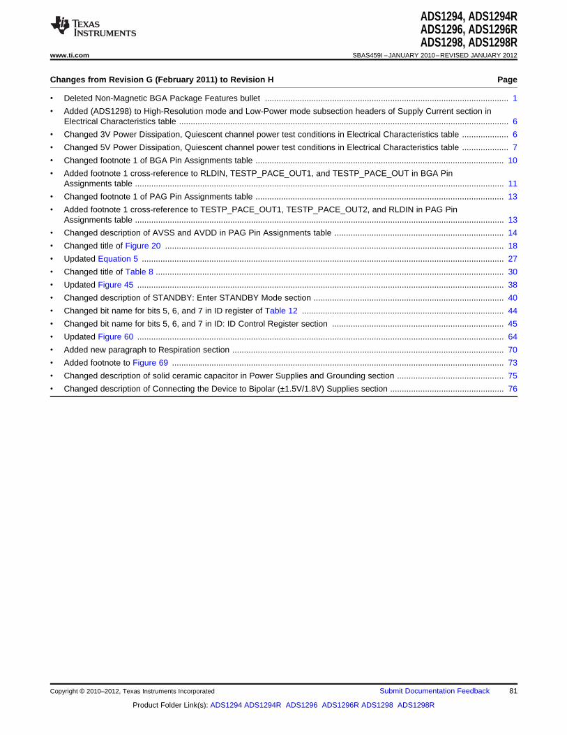
ADS1294, ADS1294RADS1296, ADS1296RADS1298, ADS1298R
www.ti.com SBAS459I –JANUARY 2010–REVISED JANUARY 2012
Changes from Revision G (February 2011) to Revision H Page
• Deleted Non-Magnetic BGA Package Features bullet ......................................................................................................... 1
• Added (ADS1298) to High-Resolution mode and Low-Power mode subsection headers of Supply Current section inElectrical Characteristics table .............................................................................................................................................. 6
• Changed 3V Power Dissipation, Quiescent channel power test conditions in Electrical Characteristics table .................... 6
• Changed 5V Power Dissipation, Quiescent channel power test conditions in Electrical Characteristics table .................... 7
• Changed footnote 1 of BGA Pin Assignments table ........................................................................................................... 10
• Added footnote 1 cross-reference to RLDIN, TESTP_PACE_OUT1, and TESTP_PACE_OUT in BGA PinAssignments table ............................................................................................................................................................... 11
• Changed footnote 1 of PAG Pin Assignments table ........................................................................................................... 13
• Added footnote 1 cross-reference to TESTP_PACE_OUT1, TESTP_PACE_OUT2, and RLDIN in PAG PinAssignments table ............................................................................................................................................................... 13
• Changed description of AVSS and AVDD in PAG Pin Assignments table ......................................................................... 14
• Changed title of Figure 20 .................................................................................................................................................. 18
• Updated Equation 5 ............................................................................................................................................................ 27
• Changed title of Table 8 ...................................................................................................................................................... 30
• Updated Figure 45 .............................................................................................................................................................. 38
• Changed description of STANDBY: Enter STANDBY Mode section .................................................................................. 40
• Changed bit name for bits 5, 6, and 7 in ID register of Table 12 ....................................................................................... 44
• Changed bit name for bits 5, 6, and 7 in ID: ID Control Register section .......................................................................... 45
• Updated Figure 60 .............................................................................................................................................................. 64
• Added new paragraph to Respiration section ..................................................................................................................... 70
• Added footnote to Figure 69 ............................................................................................................................................... 73
• Changed description of solid ceramic capacitor in Power Supplies and Grounding section .............................................. 75
• Changed description of Connecting the Device to Bipolar (±1.5V/1.8V) Supplies section ................................................. 76
Copyright © 2010–2012, Texas Instruments Incorporated Submit Documentation Feedback 81
Product Folder Link(s): ADS1294 ADS1294R ADS1296 ADS1296R ADS1298 ADS1298R
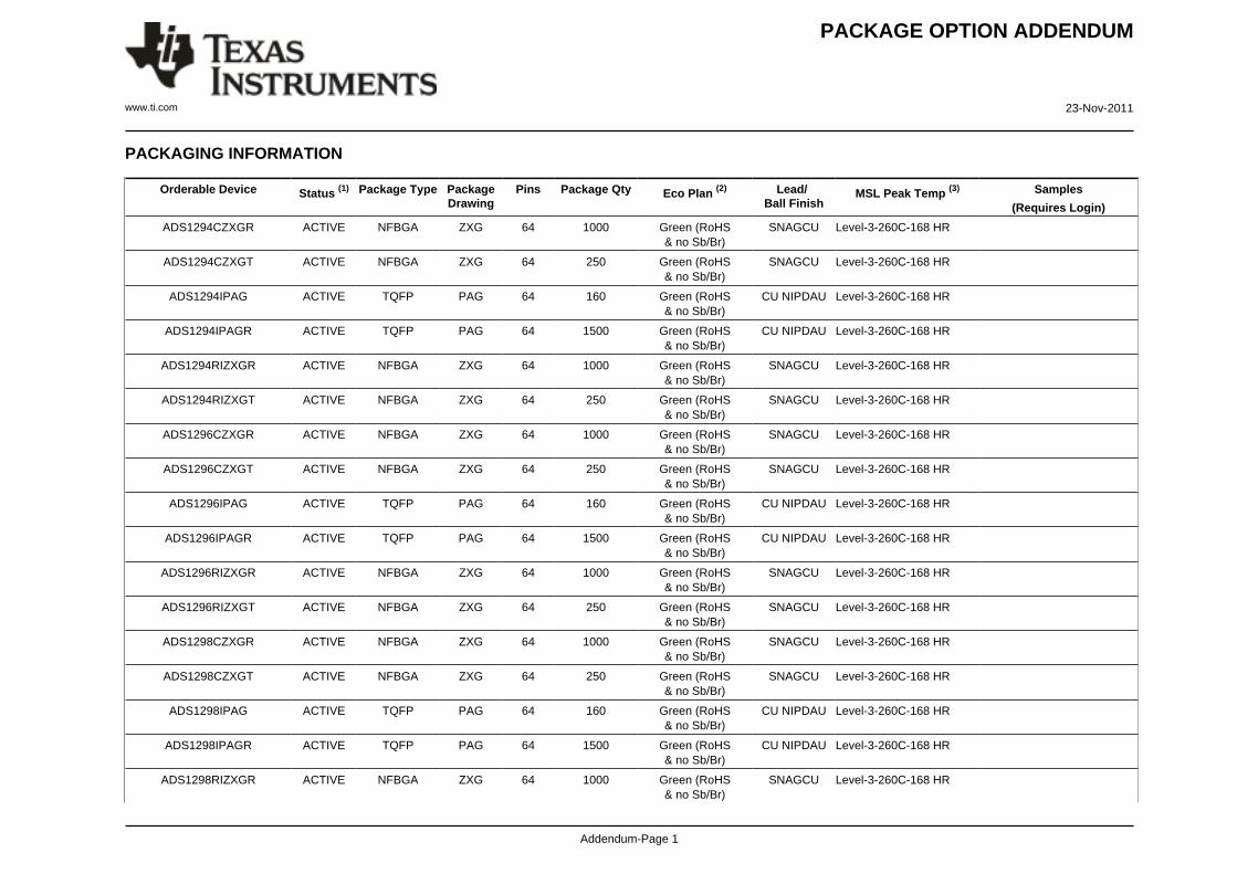
PACKAGE OPTION ADDENDUM
www.ti.com 23-Nov-2011
Addendum-Page 1
PACKAGING INFORMATION
Orderable Device Status (1) Package Type PackageDrawing
Pins Package Qty Eco Plan (2) Lead/Ball Finish
MSL Peak Temp (3) Samples
(Requires Login)
ADS1294CZXGR ACTIVE NFBGA ZXG 64 1000 Green (RoHS& no Sb/Br)
SNAGCU Level-3-260C-168 HR
ADS1294CZXGT ACTIVE NFBGA ZXG 64 250 Green (RoHS& no Sb/Br)
SNAGCU Level-3-260C-168 HR
ADS1294IPAG ACTIVE TQFP PAG 64 160 Green (RoHS& no Sb/Br)
CU NIPDAU Level-3-260C-168 HR
ADS1294IPAGR ACTIVE TQFP PAG 64 1500 Green (RoHS& no Sb/Br)
CU NIPDAU Level-3-260C-168 HR
ADS1294RIZXGR ACTIVE NFBGA ZXG 64 1000 Green (RoHS& no Sb/Br)
SNAGCU Level-3-260C-168 HR
ADS1294RIZXGT ACTIVE NFBGA ZXG 64 250 Green (RoHS& no Sb/Br)
SNAGCU Level-3-260C-168 HR
ADS1296CZXGR ACTIVE NFBGA ZXG 64 1000 Green (RoHS& no Sb/Br)
SNAGCU Level-3-260C-168 HR
ADS1296CZXGT ACTIVE NFBGA ZXG 64 250 Green (RoHS& no Sb/Br)
SNAGCU Level-3-260C-168 HR
ADS1296IPAG ACTIVE TQFP PAG 64 160 Green (RoHS& no Sb/Br)
CU NIPDAU Level-3-260C-168 HR
ADS1296IPAGR ACTIVE TQFP PAG 64 1500 Green (RoHS& no Sb/Br)
CU NIPDAU Level-3-260C-168 HR
ADS1296RIZXGR ACTIVE NFBGA ZXG 64 1000 Green (RoHS& no Sb/Br)
SNAGCU Level-3-260C-168 HR
ADS1296RIZXGT ACTIVE NFBGA ZXG 64 250 Green (RoHS& no Sb/Br)
SNAGCU Level-3-260C-168 HR
ADS1298CZXGR ACTIVE NFBGA ZXG 64 1000 Green (RoHS& no Sb/Br)
SNAGCU Level-3-260C-168 HR
ADS1298CZXGT ACTIVE NFBGA ZXG 64 250 Green (RoHS& no Sb/Br)
SNAGCU Level-3-260C-168 HR
ADS1298IPAG ACTIVE TQFP PAG 64 160 Green (RoHS& no Sb/Br)
CU NIPDAU Level-3-260C-168 HR
ADS1298IPAGR ACTIVE TQFP PAG 64 1500 Green (RoHS& no Sb/Br)
CU NIPDAU Level-3-260C-168 HR
ADS1298RIZXGR ACTIVE NFBGA ZXG 64 1000 Green (RoHS& no Sb/Br)
SNAGCU Level-3-260C-168 HR
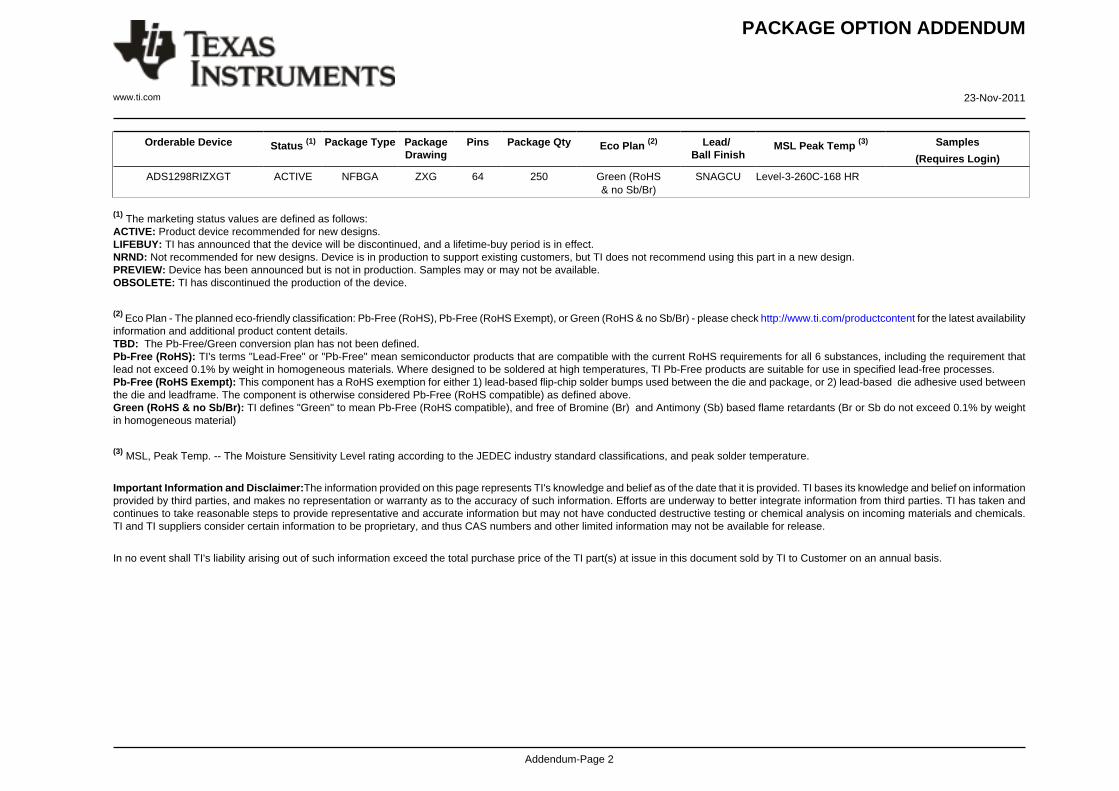
PACKAGE OPTION ADDENDUM
www.ti.com 23-Nov-2011
Addendum-Page 2
Orderable Device Status (1) Package Type PackageDrawing
Pins Package Qty Eco Plan (2) Lead/Ball Finish
MSL Peak Temp (3) Samples
(Requires Login)
ADS1298RIZXGT ACTIVE NFBGA ZXG 64 250 Green (RoHS& no Sb/Br)
SNAGCU Level-3-260C-168 HR
(1) The marketing status values are defined as follows:ACTIVE: Product device recommended for new designs.LIFEBUY: TI has announced that the device will be discontinued, and a lifetime-buy period is in effect.NRND: Not recommended for new designs. Device is in production to support existing customers, but TI does not recommend using this part in a new design.PREVIEW: Device has been announced but is not in production. Samples may or may not be available.OBSOLETE: TI has discontinued the production of the device.
(2) Eco Plan - The planned eco-friendly classification: Pb-Free (RoHS), Pb-Free (RoHS Exempt), or Green (RoHS & no Sb/Br) - please check http://www.ti.com/productcontent for the latest availabilityinformation and additional product content details.TBD: The Pb-Free/Green conversion plan has not been defined.Pb-Free (RoHS): TI's terms "Lead-Free" or "Pb-Free" mean semiconductor products that are compatible with the current RoHS requirements for all 6 substances, including the requirement thatlead not exceed 0.1% by weight in homogeneous materials. Where designed to be soldered at high temperatures, TI Pb-Free products are suitable for use in specified lead-free processes.Pb-Free (RoHS Exempt): This component has a RoHS exemption for either 1) lead-based flip-chip solder bumps used between the die and package, or 2) lead-based die adhesive used betweenthe die and leadframe. The component is otherwise considered Pb-Free (RoHS compatible) as defined above.Green (RoHS & no Sb/Br): TI defines "Green" to mean Pb-Free (RoHS compatible), and free of Bromine (Br) and Antimony (Sb) based flame retardants (Br or Sb do not exceed 0.1% by weightin homogeneous material)
(3) MSL, Peak Temp. -- The Moisture Sensitivity Level rating according to the JEDEC industry standard classifications, and peak solder temperature.
Important Information and Disclaimer:The information provided on this page represents TI's knowledge and belief as of the date that it is provided. TI bases its knowledge and belief on informationprovided by third parties, and makes no representation or warranty as to the accuracy of such information. Efforts are underway to better integrate information from third parties. TI has taken andcontinues to take reasonable steps to provide representative and accurate information but may not have conducted destructive testing or chemical analysis on incoming materials and chemicals.TI and TI suppliers consider certain information to be proprietary, and thus CAS numbers and other limited information may not be available for release.
In no event shall TI's liability arising out of such information exceed the total purchase price of the TI part(s) at issue in this document sold by TI to Customer on an annual basis.
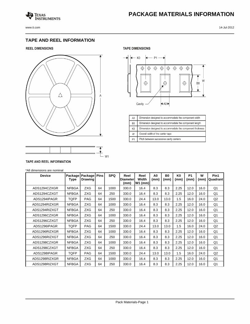
TAPE AND REEL INFORMATION
*All dimensions are nominal
Device PackageType
PackageDrawing
Pins SPQ ReelDiameter
(mm)
ReelWidth
W1 (mm)
A0(mm)
B0(mm)
K0(mm)
P1(mm)
W(mm)
Pin1Quadrant
ADS1294CZXGR NFBGA ZXG 64 1000 330.0 16.4 8.3 8.3 2.25 12.0 16.0 Q1
ADS1294CZXGT NFBGA ZXG 64 250 330.0 16.4 8.3 8.3 2.25 12.0 16.0 Q1
ADS1294IPAGR TQFP PAG 64 1500 330.0 24.4 13.0 13.0 1.5 16.0 24.0 Q2
ADS1294RIZXGR NFBGA ZXG 64 1000 330.0 16.4 8.3 8.3 2.25 12.0 16.0 Q1
ADS1294RIZXGT NFBGA ZXG 64 250 330.0 16.4 8.3 8.3 2.25 12.0 16.0 Q1
ADS1296CZXGR NFBGA ZXG 64 1000 330.0 16.4 8.3 8.3 2.25 12.0 16.0 Q1
ADS1296CZXGT NFBGA ZXG 64 250 330.0 16.4 8.3 8.3 2.25 12.0 16.0 Q1
ADS1296IPAGR TQFP PAG 64 1500 330.0 24.4 13.0 13.0 1.5 16.0 24.0 Q2
ADS1296RIZXGR NFBGA ZXG 64 1000 330.0 16.4 8.3 8.3 2.25 12.0 16.0 Q1
ADS1296RIZXGT NFBGA ZXG 64 250 330.0 16.4 8.3 8.3 2.25 12.0 16.0 Q1
ADS1298CZXGR NFBGA ZXG 64 1000 330.0 16.4 8.3 8.3 2.25 12.0 16.0 Q1
ADS1298CZXGT NFBGA ZXG 64 250 330.0 16.4 8.3 8.3 2.25 12.0 16.0 Q1
ADS1298IPAGR TQFP PAG 64 1500 330.0 24.4 13.0 13.0 1.5 16.0 24.0 Q2
ADS1298RIZXGR NFBGA ZXG 64 1000 330.0 16.4 8.3 8.3 2.25 12.0 16.0 Q1
ADS1298RIZXGT NFBGA ZXG 64 250 330.0 16.4 8.3 8.3 2.25 12.0 16.0 Q1
PACKAGE MATERIALS INFORMATION
www.ti.com 14-Jul-2012
Pack Materials-Page 1
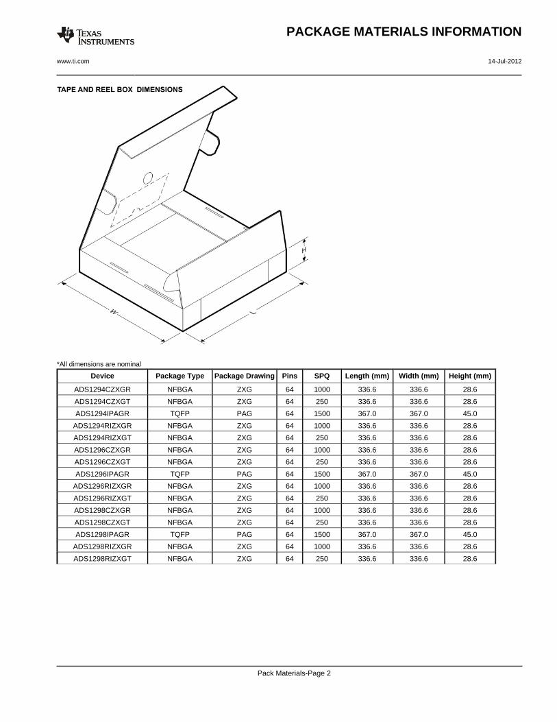
*All dimensions are nominal
Device Package Type Package Drawing Pins SPQ Length (mm) Width (mm) Height (mm)
ADS1294CZXGR NFBGA ZXG 64 1000 336.6 336.6 28.6
ADS1294CZXGT NFBGA ZXG 64 250 336.6 336.6 28.6
ADS1294IPAGR TQFP PAG 64 1500 367.0 367.0 45.0
ADS1294RIZXGR NFBGA ZXG 64 1000 336.6 336.6 28.6
ADS1294RIZXGT NFBGA ZXG 64 250 336.6 336.6 28.6
ADS1296CZXGR NFBGA ZXG 64 1000 336.6 336.6 28.6
ADS1296CZXGT NFBGA ZXG 64 250 336.6 336.6 28.6
ADS1296IPAGR TQFP PAG 64 1500 367.0 367.0 45.0
ADS1296RIZXGR NFBGA ZXG 64 1000 336.6 336.6 28.6
ADS1296RIZXGT NFBGA ZXG 64 250 336.6 336.6 28.6
ADS1298CZXGR NFBGA ZXG 64 1000 336.6 336.6 28.6
ADS1298CZXGT NFBGA ZXG 64 250 336.6 336.6 28.6
ADS1298IPAGR TQFP PAG 64 1500 367.0 367.0 45.0
ADS1298RIZXGR NFBGA ZXG 64 1000 336.6 336.6 28.6
ADS1298RIZXGT NFBGA ZXG 64 250 336.6 336.6 28.6
PACKAGE MATERIALS INFORMATION
www.ti.com 14-Jul-2012
Pack Materials-Page 2
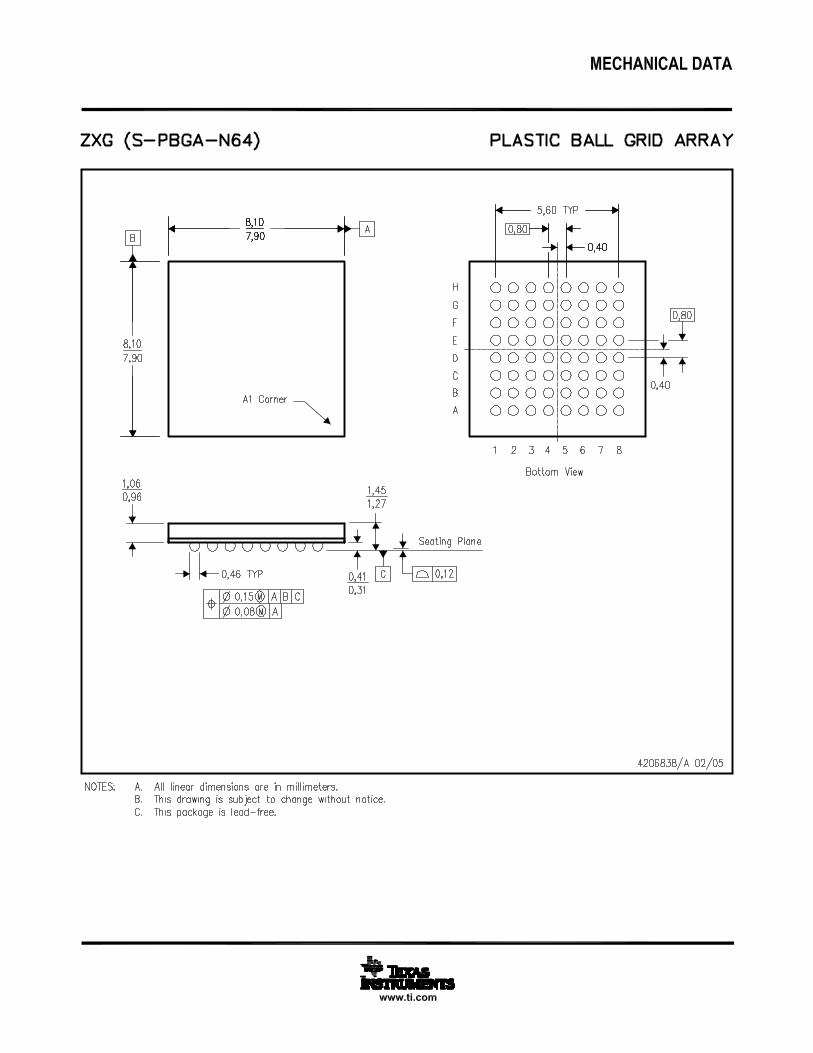
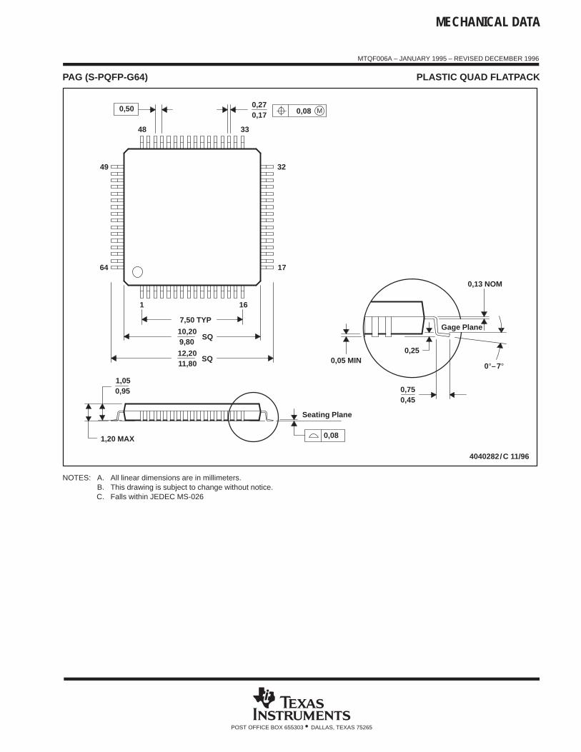
MECHANICAL DATA
MTQF006A – JANUARY 1995 – REVISED DECEMBER 1996
POST OFFICE BOX 655303 • DALLAS, TEXAS 75265
PAG (S-PQFP-G64) PLASTIC QUAD FLATPACK
0,13 NOM
0,25
0,450,75
Seating Plane
0,05 MIN
4040282/C 11/96
Gage Plane
33
0,170,27
16
48
1
7,50 TYP
49
64
SQ
9,80
1,050,95
11,8012,20
1,20 MAX
10,20SQ
17
32
0,08
0,50 M0,08
0°–7°
NOTES: A. All linear dimensions are in millimeters.B. This drawing is subject to change without notice.C. Falls within JEDEC MS-026

IMPORTANT NOTICE
Texas Instruments Incorporated and its subsidiaries (TI) reserve the right to make corrections, enhancements, improvements and otherchanges to its semiconductor products and services per JESD46C and to discontinue any product or service per JESD48B. Buyers shouldobtain the latest relevant information before placing orders and should verify that such information is current and complete. Allsemiconductor products (also referred to herein as “components”) are sold subject to TI’s terms and conditions of sale supplied at the timeof order acknowledgment.
TI warrants performance of its components to the specifications applicable at the time of sale, in accordance with the warranty in TI’s termsand conditions of sale of semiconductor products. Testing and other quality control techniques are used to the extent TI deems necessaryto support this warranty. Except where mandated by applicable law, testing of all parameters of each component is not necessarilyperformed.
TI assumes no liability for applications assistance or the design of Buyers’ products. Buyers are responsible for their products andapplications using TI components. To minimize the risks associated with Buyers’ products and applications, Buyers should provideadequate design and operating safeguards.
TI does not warrant or represent that any license, either express or implied, is granted under any patent right, copyright, mask work right, orother intellectual property right relating to any combination, machine, or process in which TI components or services are used. Informationpublished by TI regarding third-party products or services does not constitute a license to use such products or services or a warranty orendorsement thereof. Use of such information may require a license from a third party under the patents or other intellectual property of thethird party, or a license from TI under the patents or other intellectual property of TI.
Reproduction of significant portions of TI information in TI data books or data sheets is permissible only if reproduction is without alterationand is accompanied by all associated warranties, conditions, limitations, and notices. TI is not responsible or liable for such altereddocumentation. Information of third parties may be subject to additional restrictions.
Resale of TI components or services with statements different from or beyond the parameters stated by TI for that component or servicevoids all express and any implied warranties for the associated TI component or service and is an unfair and deceptive business practice.TI is not responsible or liable for any such statements.
Buyer acknowledges and agrees that it is solely responsible for compliance with all legal, regulatory and safety-related requirementsconcerning its products, and any use of TI components in its applications, notwithstanding any applications-related information or supportthat may be provided by TI. Buyer represents and agrees that it has all the necessary expertise to create and implement safeguards whichanticipate dangerous consequences of failures, monitor failures and their consequences, lessen the likelihood of failures that might causeharm and take appropriate remedial actions. Buyer will fully indemnify TI and its representatives against any damages arising out of the useof any TI components in safety-critical applications.
In some cases, TI components may be promoted specifically to facilitate safety-related applications. With such components, TI’s goal is tohelp enable customers to design and create their own end-product solutions that meet applicable functional safety standards andrequirements. Nonetheless, such components are subject to these terms.
No TI components are authorized for use in FDA Class III (or similar life-critical medical equipment) unless authorized officers of the partieshave executed a special agreement specifically governing such use.
Only those TI components which TI has specifically designated as military grade or “enhanced plastic” are designed and intended for use inmilitary/aerospace applications or environments. Buyer acknowledges and agrees that any military or aerospace use of TI componentswhich have not been so designated is solely at the Buyer's risk, and that Buyer is solely responsible for compliance with all legal andregulatory requirements in connection with such use.
TI has specifically designated certain components which meet ISO/TS16949 requirements, mainly for automotive use. Components whichhave not been so designated are neither designed nor intended for automotive use; and TI will not be responsible for any failure of suchcomponents to meet such requirements.
Products Applications
Audio www.ti.com/audio Automotive and Transportation www.ti.com/automotive
Amplifiers amplifier.ti.com Communications and Telecom www.ti.com/communications
Data Converters dataconverter.ti.com Computers and Peripherals www.ti.com/computers
DLP® Products www.dlp.com Consumer Electronics www.ti.com/consumer-apps
DSP dsp.ti.com Energy and Lighting www.ti.com/energy
Clocks and Timers www.ti.com/clocks Industrial www.ti.com/industrial
Interface interface.ti.com Medical www.ti.com/medical
Logic logic.ti.com Security www.ti.com/security
Power Mgmt power.ti.com Space, Avionics and Defense www.ti.com/space-avionics-defense
Microcontrollers microcontroller.ti.com Video and Imaging www.ti.com/video
RFID www.ti-rfid.com
OMAP Mobile Processors www.ti.com/omap TI E2E Community e2e.ti.com
Wireless Connectivity www.ti.com/wirelessconnectivity
Mailing Address: Texas Instruments, Post Office Box 655303, Dallas, Texas 75265Copyright © 2012, Texas Instruments Incorporated