24-bit, 40khz analog-to-digital converter - … 40khz analog-to-digital converter features 24...
TRANSCRIPT

24-Bit, 40kHzANALOG-TO-DIGITAL CONVERTER
FEATURES 24 BITS—NO MISSING CODES
19 BITS EFFECTIVE RESOLUTION UP TO40kHz DATA RATE
LOW NOISE: 2.5ppm
DIFFERENTIAL INPUTS
INL: 0.0015% (max)
EXTERNAL REFERENCE (0.5V to 5V)
POWER-DOWN MODE
SYNC MODE
DESCRIPTIONThe ADS1252 is a precision, wide dynamic range, delta-sigma, Analog-to-Digital (A/D) converter with 24-bit resolu-tion operating from a single +5V supply. The delta-sigmaarchitecture is used for wide dynamic range and to ensure 24bits of no missing code performance. An effective resolutionof 19 bits (2.5ppm of rms noise) is achieved for conversionrates up to 40kHz.
The ADS1252 is designed for high-resolution measurementapplications in cardiac diagnostics, smart transmitters, indus-trial process control, weight scales, chromatography, andportable instrumentation. The converter includes a flexible,2-wire synchronous serial interface for low-cost isolation.
The ADS1252 is a single-channel converter and is offered inan SO-8 package.APPLICATIONS
CARDIAC DIAGNOSTICS
DIRECT THERMOCOUPLE INTERFACES
BLOOD ANALYSIS
INFRARED PYROMETERS
LIQUID/GAS CHROMATOGRAPHY
PRECISION PROCESS CONTROL
ADS1252
SBAS127D – SEPTEMBER 2000 – REVISED JUNE 2006
www.ti.com
PRODUCTION DATA information is current as of publication date.Products conform to specifications per the terms of Texas Instrumentsstandard warranty. Production processing does not necessarily includetesting of all parameters.
Copyright © 2000-2006, Texas Instruments Incorporated
Please be aware that an important notice concerning availability, standard warranty, and use in critical applications ofTexas Instruments semiconductor products and disclaimers thereto appears at the end of this data sheet.
4th-Order∆Σ
Modulator
DigitalFilter
SerialInterface
Control
+VIN
CLK
VREF
SCLK
DOUT/DRDY
+VDD
GND
–VIN
ADS1252
ADS1252
All trademarks are the property of their respective owners.

ADS12522SBAS127Dwww.ti.com
SPECIFIEDPACKAGE TEMPERATURE PACKAGE ORDERING TRANSPORT
PRODUCT PACKAGE-LEAD DESIGNATOR RANGE MARKING NUMBER MEDIA, QUANTITY
ADS1252 SO-8 D –40°C to +85°C ADS1252U ADS1252U Rails, 100
" " " " " ADS1252U/2K5 Tape and Reel, 2500
Analog Input: Current ............................................... ±100mA, Momentary±10mA, Continuous
Voltage .................................... GND – 0.3V to VDD + 0.3VVDD to GND ............................................................................ –0.3V to 6VVREF Voltage to GND ............................................... –0.3V to VDD + 0.3VDigital Input Voltage to GND ................................... –0.3V to VDD + 0.3VDigital Output Voltage to GND ................................. –0.3V to VDD + 0.3VLead Temperature (soldering, 10s) .............................................. +300°CPower Dissipation (any package) ................................................. 500mW
NOTE: (1) Stresses above these ratings may cause permanent damage.Exposure to absolute maximum conditions for extended periods may degradedevice reliability.
ABSOLUTE MAXIMUM RATINGS(1)
PIN CONFIGURATION
Top View SO
PIN DESCRIPTIONS
PIN NAME PIN DESCRIPTION
1 +VIN Analog Input: Positive Input of the Differen-tial Analog Input
2 –VIN Analog Input: Negative Input of the Differ-ential Analog Input
3 +VDD Input: Power-Supply Voltage, +5V
4 CLK Digital Input: Device System Clock. Thesystem clock is in the form of a CMOS-compatible clock. This is a Schmitt-Triggerinput.
5 DOUT/DRDY Digital Output: Serial Data Output/DataReady. A logic LOW on this output indi-cates that a new output word is availablefrom the ADS1252 data output register.The serial data is clocked out of the serialdata output shift register using SCLK.
6 SCLK Digital Input: Serial Clock. The serial clockis in the form of a CMOS-compatible clock.The serial clock operates independentlyfrom the system clock, therefore, it is pos-sible to run SCLK at a higher frequencythan CLK. The normal state of SCLK isLOW. Holding SCLK HIGH will either ini-tiate a modulator reset for synchronizingmultiple converters or enter power-downmode. This is a Schmitt-Trigger input.
7 GND Input: Ground
8 VREF Analog Input: Reference Voltage Input
+VIN
ADS1252U
GND–VIN
VREF
+VDD SCLK
DOUT/DRDYCLK
1
2
3
4
8
7
6
5
ELECTROSTATICDISCHARGE SENSITIVITY
This integrated circuit can be damaged by ESD. Texas Instru-ments recommends that all integrated circuits be handled withappropriate precautions. Failure to observe proper handlingand installation procedures can cause damage.
ESD damage can range from subtle performance degradationto complete device failure. Precision integrated circuits may bemore susceptible to damage because very small parametricchanges could cause the device not to meet its publishedspecifications.
PACKAGE/ORDERING INFORMATION(1)
NOTE: (1) For the most current package and ordering information, see the Package Option Addendum at the end of this document, or see the TI web site at www.ti.com.

ADS1252 3SBAS127D www.ti.com
ELECTRICAL CHARACTERISTICSAll specifications at TMIN to TMAX, VDD = +5V, CLK = 16MHz, and VREF = 4.096V, unless otherwise specified.
ADS1252U
PARAMETER CONDITIONS MIN TYP MAX UNITS
ANALOG INPUTFull-Scale Input Voltage 0 ±VREF VAbsolute Input Voltage +VIN or –VIN to GND –0.3 VDD VDifferential Input Impedance CLK = 3.84kHz 125 MΩ
CLK = 1MHz 480 kΩCLK = 16MHz 30 kΩ
Input Capacitance 20 pFInput Leakage At +25°C 5 50 pA
At TMIN to TMAX 1 nA
DYNAMIC CHARACTERISTICSData Rate 41.7 kHzBandwidth –3dB 9 kHzSerial Clock (SCLK) 16 MHzSystem Clock Input (CLK) 16 MHz
ACCURACYIntegral Nonlinearity(1) ±0.0003 ±0.0015 % of FSRTHD 1kHz Input; 0.1dB below FS 97 dBNoise 2.5 3.8 ppm of FSR, rmsResolution 24 BitsNo Missing Codes 24 BitsCommon-Mode Rejection(2) at DC 90 100 dBGain Error 0.4 1 % of FSROffset Error ±100 ±200 ppm of FSRGain Sensitivity to VREF VREF = 4.096V ±0.1V 1:1Power-Supply Rejection Ratio 60 80 dB
PERFORMANCE OVER TEMPERATUREOffset Drift 0.07 ppm/°CGain Drift CLK = 16MHz 7.5 ppm/°C
CLK = 14MHz 5.2 ppm/°CCLK = 12MHz 3.9 ppm/°CCLK < 10MHz 3.4 ppm/°C
VOLTAGE REFERENCEVREF 0.5 4.096 VDD VLoad Current 220 µA
DIGITAL INPUT/OUTPUTLogic Family CMOSLogic Level: VIH +4.0 +VDD + 0.3 V
VIL –0.3 +0.8 VVOH IOH = –500µA +4.5 VVOL IOL = 500µA 0.4 V
Input (SCLK, CLK) Hysteresis 0.6 VData Format Offset Binary Two’s Complement
POWER-SUPPLY REQUIREMENTSOperation +4.75 +5 +5.25 VQuiescent Current VDD = +5VDC 8 10 mAOperating Power 40 50 mWPower-Down Current 1 10 µA
TEMPERATURE RANGEOperating –40 +85 °CStorage –60 +100 °C
NOTES: (1) Applies to full-differential signals.(2) The common-mode rejection test is performed with a 100mV differential input.

ADS12524SBAS127Dwww.ti.com
TYPICAL CHARACTERISTICSAt TA = +25°C, VDD = +5V, CLK = 16MHz, and VREF = 4.096V, unless otherwise specified.
RMS NOISE vs DATA OUTPUT RATE
Data Output Rate (Hz)
1k100 10k 100k
RM
S N
oise
(pp
m o
f FS
)
3.0
2.5
2.0
1.5
1.0
0.5
0
3.0
2.5
2.0
1.5
1.0
0.5
0
RMS NOISE vs TEMPERATURE
Temperature (°C)
–40 –20 0 20 40 60 80 100
RM
S N
oise
(pp
m o
f FS
)
10
9
8
7
6
5
4
3
2
1
0
VREF (V)
0 1 2 3 4 65
RM
S N
oise
(pp
m o
f FS
)
RMS NOISE vs VREF VOLTAGE
19.50
19.25
19.00
18.75
18.5
EFFECTIVE RESOLUTION vs DATA OUTPUT RATE
Data Output Rate (Hz)
100 1k 10k 100k
Effe
ctiv
e R
esol
utio
n (b
its)
19.0
18.9
18.8
18.7
18.6
18.5
18.4
18.3
18.2
18.1
18.0
EFFECTIVE RESOLUTION vs TEMPERATURE
Temperature (°C)
–40 –20 0 20 40 60 80 100
Effe
ctiv
e R
esol
utio
n (b
its)
25
20
15
10
5
0
VREF (V)
0 1 2 3 4 65
RM
S N
oise
(µV
)
RMS NOISE vs VREF VOLTAGE

ADS1252 5SBAS127D www.ti.com
TYPICAL CHARACTERISTICS (Cont.)At TA = +25°C, VDD = +5V, CLK = 16MHz, and VREF = 4.096V, unless otherwise specified.
4
3
2
1
0
INTEGRAL NON-LINEARITY vs DATA OUTPUT RATE
Data Output Rate (Hz)
100 1k 10k 100k
INL
(ppm
of F
S)
10
8
6
4
2
0
–2
–4
–6
–8
–10
OFFSET DRIFT vs TEMPERATURE
Offs
et D
rift (
ppm
of F
S)
Temperature (°C)
–40 –20 0 20 40 60 80 100 –40 –20 0 20 40 60 80 100
800
600
400
200
0
–200
–400
GAIN DRIFT vs TEMPERATURE
Temperature (°C)
Drif
t (pp
m)
CLK = 16MHz
CLK < 10MHz
CLK = 14.3MHz
CLK < 10MHz
CLK = 16MHz
3.0
2.5
2.0
1.5
1.0
0.5
0
RMS NOISE vs INPUT VOLTAGE
Differential Input Voltage (V)
RM
S N
oise
(pp
m o
f FS
)
–4–5 –3 –2 –1 0 1 2 3 4 5
–40 –20 0 20 40 60 80 100
4.0
3.5
3.0
2.5
2.0
1.5
1.0
0.5
0
INTEGRAL NON-LINEARITY vs TEMPERATURE
Temperature (°C)
INL
(ppm
of F
S)
19.00
18.50
18.00
17.50
17.00
16.50
VREF (V)
0 1 2 3 4 65
Effe
ctiv
e R
esol
utio
n (B
its)
EFFECTIVE RESOLUTION vs VREF

ADS12526SBAS127Dwww.ti.com
TYPICAL CHARACTERISTICS (Cont.)At TA = +25°C, VDD = +5V, CLK = 16MHz, and VREF = 4.096V, unless otherwise specified.
110
105
100
95
90
85
80
COMMON-MODE REJECTION RATIOvs CLK FREQUENCY
CLK Frequency (MHz)
0 5 10 15 20
CM
RR
(dB
)9.5
9.0
8.5
8.0
7.5
7.0
6.5
6.0
5.5
5.0
CURRENT vs TEMPERATURE
Temperature (°C)
–40 –20 0 20 40 60 80 100
Sup
ply
Cur
rent
(m
A)
45
40
35
30
25
20
15
10
5
0
POWER DISSIPATION vs CLOCK FREQUENCY
CLK Frequency (MHz)
0 5 10 15 20
Pow
er D
issi
patio
n (m
W)
0
–20
–40
–60
–80
–100
–120
–140
–160
–180
TYPICAL FFT ANALYSISOF THE 1kHz fS INPUT SIGNAL
Imput Signal Frequency (Hz)
0 2000 60004000 8000 10000 12000 14000
Dyn
amic
Ran
ge (
dB)
100
95
90
85
80
75
70
65
60
POWER-SUPPLY REJECTION RATIOvs CLK FREQUENCY
CLK Frequency (MHz)
0 5 10 15 20
PS
RR
(dB
)

ADS1252 7SBAS127D www.ti.com
THEORY OF OPERATIONThe ADS1252 is a precision, high-dynamic range, 24-bit, delta-sigma, A/D converter capable of achieving very high-resolutiondigital results at high data rates. The analog-input signalis sampled at a rate determined by the frequency of the systemclock (CLK). The sampled analog input is modulated bythe delta-sigma A/D modulator, which is followed by a digitalfilter. A Sinc5 digital low-pass filter processes the output ofthe delta-sigma modulator and writes the result into the data-output register. The DOUT/DRDY pin is pulled LOW, indicatingthat new data is available to be read by the externalmicrocontroller/microprocessor. As shown in the block dia-gram, the main functional blocks of the ADS1252 are the4th-order delta-sigma modulator, a digital filter, control logic,and a serial interface. Each of these functional blocks isdescribed below.
ANALOG INPUT
The ADS1252 contains a fully differential analog input. Inorder to provide low system noise, common-mode rejectionof 100dB, and excellent power-supply rejection, the designtopology is based on a fully differential switched-capacitorarchitecture. The bipolar input voltage range is from –4.096to +4.096V, when the reference input voltage equals +4.096V;the bipolar range is with respect to –VIN, and not with respectto GND.
With regard to the analog input signal, the overall analogperformance of the device is affected by three items. First,the input impedance can affect accuracy; therefore, if thesource impedance of the input signal is significant, or if thereis passive filtering prior to the ADS1252, a significant portionof the signal can be lost across this external impedance. Themagnitude of the effect is dependent on the desired systemperformance. See application note Understanding theADS1251, ADS1253, and ADS1254 Input Circuitry(SBAA086), available for download from TI’s web site,www.ti.com.
Second, the current into or out of the analog inputs must belimited. Under no conditions should the current into or out ofthe analog inputs exceed 10mA.
Third, to prevent aliasing of the input signal, the bandwidth ofthe analog input signal must be band limited; the bandwidthis a function of the system clock frequency. With a systemclock frequency of 16MHz, the data-output rate is 41.667kHzwith a –3dB frequency of 9kHz, where the –3dB frequencyscales with the system clock frequency.
To ensure the best linearity of the ADS1252, a fully differen-tial signal is recommended.
BIPOLAR INPUT
The differential inputs of the ADS1252 are designed toaccept differential signals; however, each analog input volt-age must stay between –0.3V and VDD. With a referencevoltage at less than half of VDD, one input can be tied to thereference voltage, and the other input can range from 0V to2 • VREF. By using a single op amp circuit featuring a singleamplifier and four external resistors, the ADS1252 can beconfigured to accept bipolar inputs referenced to ground. Theconventional ±2.5V, ±5V, and ±10V input ranges can beinterfaced to the ADS1252 using the resistor values shown inFigure 1.
FIGURE 1. Level Shift Circuit for Bipolar Input Ranges.
10kΩ
20kΩ
R1
OPA2350
OPA2350
+IN
–IN VREF
ADS1252
R2
Bipolar Input
REF2.5V
BIPOLAR INPUT R1 R2
±10V 2.5kΩ 5kΩ±5V 5kΩ 10kΩ
±2.5V 10kΩ 20kΩ
ADS12528SBAS127Dwww.ti.com
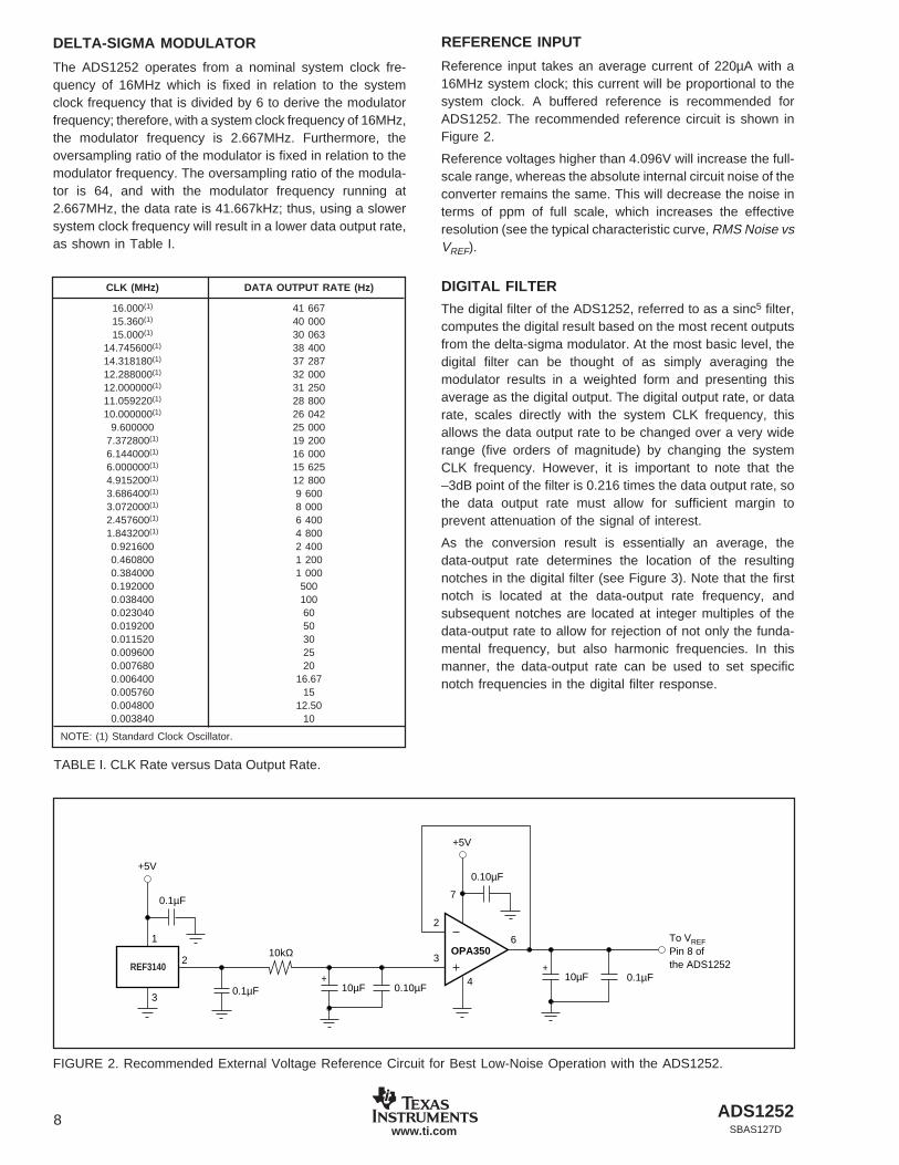
FIGURE 2. Recommended External Voltage Reference Circuit for Best Low-Noise Operation with the ADS1252.
DELTA-SIGMA MODULATOR
The ADS1252 operates from a nominal system clock fre-quency of 16MHz which is fixed in relation to the systemclock frequency that is divided by 6 to derive the modulatorfrequency; therefore, with a system clock frequency of 16MHz,the modulator frequency is 2.667MHz. Furthermore, theoversampling ratio of the modulator is fixed in relation to themodulator frequency. The oversampling ratio of the modula-tor is 64, and with the modulator frequency running at2.667MHz, the data rate is 41.667kHz; thus, using a slowersystem clock frequency will result in a lower data output rate,as shown in Table I.
TABLE I. CLK Rate versus Data Output Rate.
CLK (MHz) DATA OUTPUT RATE (Hz)
16.000(1) 41 66715.360(1) 40 00015.000(1) 30 063
14.745600(1) 38 40014.318180(1) 37 28712.288000(1) 32 00012.000000(1) 31 25011.059220(1) 28 80010.000000(1) 26 042
9.600000 25 0007.372800(1) 19 2006.144000(1) 16 0006.000000(1) 15 6254.915200(1) 12 8003.686400(1) 9 6003.072000(1) 8 0002.457600(1) 6 4001.843200(1) 4 8000.921600 2 4000.460800 1 2000.384000 1 0000.192000 5000.038400 1000.023040 600.019200 500.011520 300.009600 250.007680 200.006400 16.670.005760 150.004800 12.500.003840 10
NOTE: (1) Standard Clock Oscillator.
REFERENCE INPUT
Reference input takes an average current of 220µA with a16MHz system clock; this current will be proportional to thesystem clock. A buffered reference is recommended forADS1252. The recommended reference circuit is shown inFigure 2.
Reference voltages higher than 4.096V will increase the full-scale range, whereas the absolute internal circuit noise of theconverter remains the same. This will decrease the noise interms of ppm of full scale, which increases the effectiveresolution (see the typical characteristic curve, RMS Noise vsVREF).
DIGITAL FILTER
The digital filter of the ADS1252, referred to as a sinc5 filter,computes the digital result based on the most recent outputsfrom the delta-sigma modulator. At the most basic level, thedigital filter can be thought of as simply averaging themodulator results in a weighted form and presenting thisaverage as the digital output. The digital output rate, or datarate, scales directly with the system CLK frequency, thisallows the data output rate to be changed over a very widerange (five orders of magnitude) by changing the systemCLK frequency. However, it is important to note that the–3dB point of the filter is 0.216 times the data output rate, sothe data output rate must allow for sufficient margin toprevent attenuation of the signal of interest.
As the conversion result is essentially an average, thedata-output rate determines the location of the resultingnotches in the digital filter (see Figure 3). Note that the firstnotch is located at the data-output rate frequency, andsubsequent notches are located at integer multiples of thedata-output rate to allow for rejection of not only the funda-mental frequency, but also harmonic frequencies. In thismanner, the data-output rate can be used to set specificnotch frequencies in the digital filter response.
0.10µF
+5V
10kΩ
10µF4
3
2
7
6
+0.10µF
0.1µF10µF+
0.1µF
OPA350
0.1µF
+5V
3
1
2
To VREFPin 8 ofthe ADS1252REF3140

ADS1252 9SBAS127D www.ti.com
The digital filter requires five conversions to fully settle. Themodulator has an oversampling ratio of 64; therefore, itrequires 5 • 64, or 320 modulator results, or clocks, to fullysettle. As the modulator clock is derived from the systemclock (CLK) (modulator clock = CLK ÷ 6), the number ofsystem clocks required for the digital filter to fully settle is5 • 64 • 6, or 1920 CLKs. This means that any significant stepchange at the analog input requires five full conversions tosettle. However, if the analog input change occurs asynchro-nously to the DOUT/DRDY pulse, then six conversions arerequired to ensure full settling.
CONTROL LOGIC
The control logic is used for communications and control ofthe ADS1252.
Power-Up Sequence
Prior to power-up, all digital and analog-input pins must beLOW. At the time of power-up, these signal inputs can bebiased to a voltage other than 0V, however, they must neverexceed +VDD.
Once the ADS1252 powers up, the DOUT/DRDY line pulsesLOW on the first conversion; this data is not valid. The sixthpulse of DOUT/DRDY is valid data from the analog inputsignal.
DOUT/DRDY
The DOUT/DRDY output signal alternates between twomodes of operation. The first mode of operation is the DataReady (DRDY) mode to indicate that new data has beenloaded into the data-output register and is ready to be read.The second mode of operation is the Data Output (DOUT)mode and is used to serially shift data out of the Data OutputRegister (DOR). See Figure 11 for the time domain partition-ing of the DRDY and DOUT function.
See Figure 12 for the basic timing of DOUT/DRDY. Duringthe time defined by t2, t3, and t4, the DOUT/DRDYpin functions in DRDY mode. The state of theDOUT/DRDY pin is HIGH prior to the internal transfer of newdata to the DOR. The result of the A/D conversion is written
For example, if the rejection of power-line frequencies isdesired, then the data-output rate can simply be set to thepower-line frequency. For 50Hz rejection, the system CLKfrequency must be 19.200kHz, and this will set the data-output rate to 50Hz (see Table I and Figure 4). For 60Hzrejection, the system CLK frequency must be 20.040kHz,and this will set the data-output rate to 60Hz (see Table I andFigure 5). If both 50Hz and 60Hz rejection is required, thenthe system CLK must be 3.840kHz; this will set the data-output rate to 10Hz and reject both 50Hz and 60Hz (see TableI and Figure 6).
There is an additional benefit in using a lower data-outputrate: it provides better rejection of signals in the frequencyband of interest. For example, with a 50Hz data-output rate,a significant signal at 75Hz can alias back into the passbandat 25Hz; this is due to the fact that rejection at 75Hz mustonly be 66dB in the stopband—frequencies higher than thefirst-notch frequency (see Figure 4). However, setting thedata-output rate to 10Hz will provide 135dB rejection at 75Hz(see Figure 6). A similar benefit is gained at frequencies nearthe data-output rate (see Figures 7, 8, 9, and 10). Forexample, with a 50Hz data-output rate, rejection at 55Hz mayonly be 105dB (see Figure 7); however, with a 10Hz data-output rate, rejection at 55Hz will be 122dB (see Figure 8).If a slower data-output rate does not meet the systemrequirements, then the analog front end can be designed toprovide the needed attenuation to prevent aliasing. Addition-ally, the data-output rate can be increased and additionaldigital filtering can be done in the processor or controller.
Application note SBAA103, A Spreadsheet to Calculate theFrequency Response of the ADS1250-54 (available for down-load at www.ti.com) provides a simple tool for calculating theADS1250 frequency response for any CLK frequency.
The digital filter is described by the following transfer func-tion:
H f
ff
ff
or
H zz
z
MOD
MOD
( )
sin• •
• sin•
( )–
• –
–
–
=
= ( )
π
π
64
64
1
64 1
5
64
1
5

ADS125210SBAS127Dwww.ti.com
DIGITAL FILTER RESPONSE0
–20
–40
–60
–80
–100
–120
–140
–160
–180
–20046 47 48 49 50 51 52 53 54 5545
Frequency (Hz)
Gai
n (d
B)
DIGITAL FILTER RESPONSE0
–20
–40
–60
–80
–100
–120
–140
–160
–180
–20046 47 48 49 50 51 52 53 54 5545
Frequency (Hz)
Gai
n (d
B)
FIGURE 7. Expanded Digital Filter Response (50Hz with a50Hz Notch).
FIGURE 8. Expanded Digital Filter Response (50Hz with a10Hz Notch).
DIGITAL FILTER RESPONSE0
–20
–40
–60
–80
–100
–120
–140
–160
–180
–20050 100 150 200 250 3000
Frequency (Hz)
Gai
n (d
B)
DIGITAL FILTER RESPONSE0
–20
–40
–60
–80
–100
–120
–140
–160
–180
–20010 20 30 40 50 60 70 80 90 1000
Frequency (Hz)
Gai
n (d
B)
FIGURE 5. Digital Filter Response (60Hz). FIGURE 6. Digital Filter Response (10Hz Multiples).
FIGURE 3. Normalized Digital Filter Response.
NORMALIZED DIGITAL FILTER RESPONSE0
–20
–40
–60
–80
–100
–120
–140
–160
–180
–2001 2 3 4 5 6 7 8 9 100
Frequency (Hz)
Gai
n (d
B)
DIGITAL FILTER RESPONSE0
–20
–40
–60
–80
–100
–120
–140
–160
–180
–20050 100 150 200 250 3000
Frequency (Hz)
Gai
n (d
B)
FIGURE 4. Digital Filter Response (50Hz).

ADS1252 11SBAS127D www.ti.com
DIGITAL FILTER RESPONSE0
–20
–40
–60
–80
–100
–120
–140
–160
–180
–20056 57 58 59 60 61 62 63 64 6555
Frequency (Hz)
Gai
n (d
B)
DIGITAL FILTER RESPONSE0
–20
–40
–60
–80
–100
–120
–140
–160
–180
–20056 57 58 59 60 61 62 63 64 6555
Frequency (Hz)
Gai
n (d
B)
FIGURE 9. Expanded Digital Filter Response (60Hz with a60Hz Notch).
FIGURE 10. Expanded Digital Filter Response (60Hz with a10Hz Notch).
to the DOR from MSB to LSB in the time defined by t1 (seeFigures 11 and 12). The DOUT/DRDY line then drives theline LOW for the time defined by t2, and then drives the lineHIGH for the time defined by t3 to indicate that new data isavailable to be read. At this point, the function of the DOUT/DRDY pin changes to DOUT mode, and data is shifted outon the pin after t7. If the MSB is high (because of a negativeresult) the DOUT/DRDY signal will stay HIGH after the endof time t3. The device communicating with the ADS1252 canprovide SCLKs to the ADS1252 after the time defined by t6.The normal mode of reading data from the ADS1252 is forthe device reading the ADS1252 to latch the data on therising edge of SCLK (since data is shifted out of the ADS1252on the falling edge of SCLK). In order to retrieve valid data,the entire DOR must be read before the DOUT/DRDY pinreverts back to DRDY mode.
If SCLKs are not provided to the ADS1252 during the DOUTmode, the MSB of the DOR is present on the DOUT/DRDYline until the beginning of the time defined by t4. If anincomplete read of the ADS1252 takes place in DOUT mode(that is, fewer than 24 SCLKs are provided), the state of thelast bit read is present on the DOUT/DRDY line until thebeginning of the time defined by t4. If more than 24 SCLKsare provided during DOUT mode, the DOUT/DRDY linestays LOW until the beginning of the time defined by t4.
The internal data pointer for shifting data out onDOUT/DRDY is reset on the falling edge of the time definedby t1 and t4. This ensures that the first bit of data shifted outof the ADS1252 after DRDY mode is always the MSB of newdata.
SYNCHRONIZING MULTIPLE CONVERTERS
The normal state of SCLK is LOW; however, by holding SCLKHIGH, multiple ADS1252s can be synchronized. This is ac-complished by holding SCLK HIGH for at least four, but lessthan 20, consecutive DOUT/DRDY cycles (see Figure 13).After the ADS1252 circuitry detects that SCLK has been heldHIGH for four consecutive DOUT/DRDY cycles, the DOUT/DRDY pin pulses LOW for 3 CLK cycles and then held HIGH,and the modulator is held in a reset state. The modulatoris released from reset and synchronization occurs on thefalling edge of SCLK. It is important to note that priorto synchronization, the DOUT/DRDY pulse of multipleADS1252s in the system can have a difference in timing upto one DRDY period. Therefore, to ensure synchronization,the SCLK must be held HIGH for at least five DRDY cycles.The first DOUT/DRDY pulse after the falling edge ofSCLK occurs at t14. Valid data is not present until the sixthDOUT/DRDY pulse.

ADS125212SBAS127Dwww.ti.com
POWER-DOWN MODE
The normal state of SCLK is LOW; however, by holdingSCLK HIGH, the ADS1252 enters power-down mode. This isaccomplished by holding SCLK HIGH for at least 20 con-secutive DOUT/DRDY periods (see Figure 14). After theADS1252 circuitry detects that SCLK is held HIGH for fourconsecutive DOUT/DRDY cycles, the DOUT/DRDY pin pulsesLOW for three CLK cycles, then held HIGH, and the modu-lator will be held in a reset state. If SCLK is held HIGH for anadditional 16 DOUT/DRDY periods, the ADS1252 enterspower-down mode and the part is released from power-downmode on the falling edge of SCLK. It is important to note thatthe DOUT/DRDY pin is held HIGH after four DOUT/DRDYcycles, but power-down mode is not entered for an additional16 DOUT/DRDY periods. The first DOUT/DRDY pulse afterthe falling edge of SCLK occurs at t16; however, subsequentDOUT/DRDY pulses occur normally. Valid data is not presentuntil the sixth DOUT/DRDY pulse.
SERIAL INTERFACE
The ADS1252 includes a simple serial interface which can beconnected to microcontrollers and digital signal processors ina variety of ways. Communications with the ADS1252 cancommence on the first detection of the DOUT/DRDY pulseafter power up, although data is valid until the sixth conver-sion.
It is important to note that the data from the ADS1252 is a24-bit result transmitted MSB-first in Offset Binary Two’sComplement format, as shown in Table III.
The data must be clocked out before the ADS1252 entersDRDY mode to ensure reception of valid data, as describedin the DOUT/DRDY section of this data sheet.
FIGURE 11. DOUT/DRDY Partitioning.
DATA
DRDY Mode DOUT ModeDOUT Mode
DATA DATA
t4t2 t3
t1
DRDY Mode
DOUT/DRDY
TABLE III. ADS1252 Data Format (Offset Binary Two'sComplement).
DIFFERENTIAL VOLTAGE INPUT DIGITAL OUTPUT (HEX)
+Full-Scale 7FFFFFH
Zero 000000H
–Full-Scale 800000H
SYMBOL DESCRIPTION MIN TYP MAX UNITS
tDRDY Conversion Cycle 384 • CLK nsDRDY Mode DRDY Mode 36 • CLK nsDOUT Mode DOUT Mode 348 • CLK ns
t1 DOR Write Time 6 • CLK nst2 DOUT/DRDY LOW Time 6 • CLK nst3 DOUT/DRDY HIGH Time (Prior to Data Out) 6 • CLK nst4 DOUT/DRDY HIGH Time (Prior to Data Ready) 24 • CLK nst5 Rising Edge of CLK to Falling Edge of DOUT/DRDY 30 nst6 End of DRDY Mode to Rising Edge of First SCLK 30 nst7 End of DRDY Mode to Data Valid (Propagation Delay) 30 nst8 Falling Edge of SCLK to Data Valid (Hold Time) 5 nst9 Falling Edge of SCLK to Next Data Out Valid (Propagation Delay) 30 nst10 SCLK Setup Time for Synchronization or Power Down 30 nst11 DOUT/DRDY Pulse for Synchronization or Power Down 3 • CLK nst12 Rising Edge of SCLK Until Start of Synchronization 1537 • CLK 7679 • CLK nst13 Synchronization Time 0.5 • CLK 6143.5 • CLK nst14 Falling Edge of CLK (After SCLK Goes LOW) Until Start of DRDY Mode 2042.5 • CLK nst15 Rising Edge of SCLK Until Start of Power Down 7681 • CLK nst16 Falling Edge of CLK (After SCLK Goes LOW) Until Start of DRDY Mode 591.5 • CLK 592.5 • CLK nst17 Falling Edge of Last DOUT/DRDY to Start of Power Down 6143.5 • CLK ns
TABLE II. Digital Timing.

ADS1252 13SBAS127D www.ti.com
FIG
UR
E 1
2. D
OU
T/D
RD
Y T
imin
g.
FIG
UR
E 1
4. P
ower
-Dow
n M
ode.
FIG
UR
E 1
3. S
ynch
roni
zatio
n M
ode.
CLK
DO
UT
/DR
DY
SC
LK
t 5
t 1
t 2t 3
t 4
t 7
t 6
t 8 t 9
DR
DY
Mod
eD
OU
T M
ode
t DR
DY
MS
BLS
B
CLK
DO
UT
/DR
DY
SC
LK
t 3t 4
t 12
t 2t 1
1
t 13
t 14
t DR
DY
t 10
t DR
DY
4 t D
RD
Y
DA
TAD
ATA
DA
TA
Syn
chro
niza
tion
Mod
e S
tart
s H
ere
Syn
chro
niza
tion
Beg
ins
Her
e
DO
UT
Mod
et 3
t 4t 2
DO
UT
Mod
e
CLK
DO
UT
/DR
DY
SC
LK
t 3t 4
t 15
t 2t 1
1
t 17
t 16
t DR
DY
t 10
t DR
DY
4 t D
RD
Y
DA
TAD
ATA
DA
TA
Pow
er D
own
Occ
urs
Her
e
DO
UT
Mod
et 3
t 4t 2
DO
UT
Mod
et 1
1

ADS125214SBAS127Dwww.ti.com
ISOLATIONThe serial interface of the ADS1252 provides for simpleisolation methods. The CLK signal can be local to theADS1252, which then only requires two signals (SCLK andDOUT/DRDY) to be used for isolated data acquisition.
LAYOUTPOWER SUPPLYThe power supply should be well regulated and low noise.For designs requiring very high resolution from the ADS1252,power-supply rejection will be a concern. Avoid runningdigital lines under the device because they can couple noiseonto the die. High-frequency noise can capacitively coupleinto the analog portion of the device and will alias back intothe passband of the digital filter, affecting the conversionresult.
GROUNDINGThe analog and digital sections of the system design must becarefully and cleanly partitionedl; each section must have itsown ground plane with no overlap between them. GND mustbe connected to the analog ground plane, as well as all otheranalog grounds. Do not join the analog and digital groundplanes on the board, but instead connect the two with amoderate signal trace. For multiple converters, connect thetwo ground planes at one location as central to all of theconverters as possible. In some cases, experimentation isrequired to find the best point to connect the two planestogether. The printed circuit board can be designed to pro-vide different analog/digital ground connections via shortjumpers; the initial prototype can be used to establish whichconnection works best.
DECOUPLINGGood decoupling practices must be used for the ADS1252and for all components in the design. All decoupling capaci-tors, and specifically the 0.1µF ceramic capacitors, must beplaced as close as possible to the pin being decoupled. A1µF to 10µF capacitor, in parallel with a 0.1µF ceramiccapacitor, must be used to decouple VDD to GND.
SYSTEM CONSIDERATIONSThe recommendations for power supplies and groundingchange depending on the requirements and specific designof the overall system. Achieving 24 bits of noise performanceis a great deal more difficult than achieving 12 bits of noiseperformance. In general, a system can be broken up into fourdifferent stages:
• Analog Processing• Analog Portion of the ADS1252• Digital Portion of the ADS1252• Digital Processing
For the simplest system consisting of minimal analog signalprocessing (basic filtering and gain), a microcontroller, andone clock source, one can achieve high resolution by power-ing all components by a common power supply. In addition,all components can share a common ground plane; thus,there would be no distinctions between analog power andground, and digital power and ground. The layout must stillinclude a power plane, a ground plane, and careful decoupling.In a more extreme case, the design can include:
• Multiple ADS1252s• Extensive Analog Signal Processing• One or More Microcontrollers, Digital Signal Processors, or
Microprocessors• Many Different Clock Sources• Interconnections to Various Other Systems
High resolution will be very difficult to achieve for this design.The approach would be to break the system into as manydifferent parts as possible. For example, each ADS1252 mayhave its own analog processing front end.
DEFINITION OF TERMS
An attempt has been made to be consistent with the termi-nology used in this data sheet. In that regard, the definitionof each term is given as follows:
Analog-Input Differential Voltage—for an analog signalthat is fully differential, the voltage range can be compared tothat of an instrumentation amplifier. For example, if bothanalog inputs of the ADS1252 are at 2.048V, the differentialvoltage is 0V; however, if one analog input is at 0V and theother analog input is at 4.096V, then the differential voltagemagnitude is 4.096V. This is the case regardless of whichinput is at 0V and which is at 4.096V. The digital-output

ADS1252 15SBAS127D www.ti.com
N NOISE ER ER(NUMBER REDUCTION IN IN
OF AVERAGES) FACTOR µVrms BITS rms
1 1 31.3µV 182 1.414 22.1µV 18.54 2 15.6µV 198 2.82 11.1µV 19.516 4 7.82µV 2032 5.66 5.53µV 20.564 8 3.91µV 21128 11.3 2.77µV 21.5256 16 1.96µV 22512 22.6 1.38µV 22.5
1024 32 978nV 232048 45.25 692nV 23.54096 64 489nV 24
TABLE IV. Averaging.
result, however, is quite different. The analog-input differen-tial voltage is given by the following equation:
+VIN – (–VIN)
A positive digital output is produced whenever theanalog-input differential voltage is positive, whereas negativedigital output is produced whenever the differential is nega-tive. For example, a positive full-scale output is producedwhen the converter is configured with a 4.096V reference,and the analog-input differential is 4.096V, the negative full-scale output is produced when the differential voltage is–4.096V. In each case, the actual input voltages must remainwithin the –0.3V to +VDD range.
Actual Analog-Input Voltage—the voltage at any one ana-log input relative to GND.
Full-Scale Range (FSR)—as with most A/D converters, thefull-scale range of the ADS1252 is defined as the input whichproduces the positive full-scale digital output minus the inputwhich produces the negative full-scale digital output. Forexample, when the converter is configured with a 4.096Vreference, the differential full-scale range is:
[4.096V (positive full-scale) – (–4.096V) (negative full-scale)] = 8.192V
Least Significant Bit (LSB) Weight—this is the theoreticalamount of voltage that the differential voltage at the analoginput has to change in order to observe a change in theoutput data of one least significant bit. It is computed asfollows:
LSB WeightFull ScaleRange
N= −2
where N is the number of bits in the digital output.
Conversion Cycle—as used here, a conversion cycle refersto the time period between DOUT/DRDY pulses.
Effective Resolution (ER)—of the ADS1252 in a particularconfiguration can be expressed in two different units:bits rms (referenced to output) and µVrms (referenced toinput). Computed directly from the converter output data,
each is a statistical calculation based on a given number ofresults. Noise occurs randomly; the rms value represents astatistical measure which is one standard deviation. The ERin bits can be computed as follows:
ER in bits rms =
20 log2• •
VVrms noise
REF
6 02.
The 2 • VREF figure in each calculation represents thefull-scale range of the ADS1252, this means that both unitsare absolute expressions of resolution—the performance indifferent configurations can be directly compared, regardlessof the units.
Noise Reduction—for random noise, the ER can be im-proved with averaging. The result is the reduction in noise bythe factor √N, where N is the number of averages, as shownin Table IV; this can be used to achieve true 24-bit perfor-mance at a lower data rate. To achieve 24 bits of resolution,more than 24 bits must be accumulated. A 36-bit accumula-tor is required to achieve an ER of 24 bits. The following usesVREF = 4.096V, with the ADS1252 outputting data at 40kHz,a 4096 point average takes 102.4ms. The benefits of averag-ing is degraded if the input signal drifts during that 100ms.

ADS125216SBAS127Dwww.ti.com
DATE REVISION PAGE SECTION DESCRIPTION
11 DOUT/DRDY Text changes to DOUT/DRDY section.
Revision History
NOTE: Page numbers for previous revisions may differ from page numbers in the current version.
6/06 D

PACKAGE OPTION ADDENDUM
www.ti.com 30-Jun-2016
Addendum-Page 1
PACKAGING INFORMATION
Orderable Device Status(1)
Package Type PackageDrawing
Pins PackageQty
Eco Plan(2)
Lead/Ball Finish(6)
MSL Peak Temp(3)
Op Temp (°C) Device Marking(4/5)
Samples
ADS1252U ACTIVE SOIC D 8 75 Green (RoHS& no Sb/Br)
CU NIPDAU Level-2-260C-1 YEAR -40 to 85 ADS1252U
ADS1252U/2K5 ACTIVE SOIC D 8 2500 Green (RoHS& no Sb/Br)
CU NIPDAU Level-2-260C-1 YEAR -40 to 85 ADS1252U
ADS1252U/2K5G4 ACTIVE SOIC D 8 2500 Green (RoHS& no Sb/Br)
CU NIPDAU Level-2-260C-1 YEAR -40 to 85 ADS1252U
ADS1252UG4 ACTIVE SOIC D 8 75 Green (RoHS& no Sb/Br)
CU NIPDAU Level-2-260C-1 YEAR -40 to 85 ADS1252U
(1) The marketing status values are defined as follows:ACTIVE: Product device recommended for new designs.LIFEBUY: TI has announced that the device will be discontinued, and a lifetime-buy period is in effect.NRND: Not recommended for new designs. Device is in production to support existing customers, but TI does not recommend using this part in a new design.PREVIEW: Device has been announced but is not in production. Samples may or may not be available.OBSOLETE: TI has discontinued the production of the device.
(2) Eco Plan - The planned eco-friendly classification: Pb-Free (RoHS), Pb-Free (RoHS Exempt), or Green (RoHS & no Sb/Br) - please check http://www.ti.com/productcontent for the latest availabilityinformation and additional product content details.TBD: The Pb-Free/Green conversion plan has not been defined.Pb-Free (RoHS): TI's terms "Lead-Free" or "Pb-Free" mean semiconductor products that are compatible with the current RoHS requirements for all 6 substances, including the requirement thatlead not exceed 0.1% by weight in homogeneous materials. Where designed to be soldered at high temperatures, TI Pb-Free products are suitable for use in specified lead-free processes.Pb-Free (RoHS Exempt): This component has a RoHS exemption for either 1) lead-based flip-chip solder bumps used between the die and package, or 2) lead-based die adhesive used betweenthe die and leadframe. The component is otherwise considered Pb-Free (RoHS compatible) as defined above.Green (RoHS & no Sb/Br): TI defines "Green" to mean Pb-Free (RoHS compatible), and free of Bromine (Br) and Antimony (Sb) based flame retardants (Br or Sb do not exceed 0.1% by weightin homogeneous material)
(3) MSL, Peak Temp. - The Moisture Sensitivity Level rating according to the JEDEC industry standard classifications, and peak solder temperature.
(4) There may be additional marking, which relates to the logo, the lot trace code information, or the environmental category on the device.
(5) Multiple Device Markings will be inside parentheses. Only one Device Marking contained in parentheses and separated by a "~" will appear on a device. If a line is indented then it is a continuationof the previous line and the two combined represent the entire Device Marking for that device.
(6) Lead/Ball Finish - Orderable Devices may have multiple material finish options. Finish options are separated by a vertical ruled line. Lead/Ball Finish values may wrap to two lines if the finishvalue exceeds the maximum column width.

PACKAGE OPTION ADDENDUM
www.ti.com 30-Jun-2016
Addendum-Page 2
Important Information and Disclaimer:The information provided on this page represents TI's knowledge and belief as of the date that it is provided. TI bases its knowledge and belief on informationprovided by third parties, and makes no representation or warranty as to the accuracy of such information. Efforts are underway to better integrate information from third parties. TI has taken andcontinues to take reasonable steps to provide representative and accurate information but may not have conducted destructive testing or chemical analysis on incoming materials and chemicals.TI and TI suppliers consider certain information to be proprietary, and thus CAS numbers and other limited information may not be available for release.
In no event shall TI's liability arising out of such information exceed the total purchase price of the TI part(s) at issue in this document sold by TI to Customer on an annual basis.

TAPE AND REEL INFORMATION
*All dimensions are nominal
Device PackageType
PackageDrawing
Pins SPQ ReelDiameter
(mm)
ReelWidth
W1 (mm)
A0(mm)
B0(mm)
K0(mm)
P1(mm)
W(mm)
Pin1Quadrant
ADS1252U/2K5 SOIC D 8 2500 330.0 12.4 6.4 5.2 2.1 8.0 12.0 Q1
PACKAGE MATERIALS INFORMATION
www.ti.com 12-Jan-2018
Pack Materials-Page 1

*All dimensions are nominal
Device Package Type Package Drawing Pins SPQ Length (mm) Width (mm) Height (mm)
ADS1252U/2K5 SOIC D 8 2500 367.0 367.0 35.0
PACKAGE MATERIALS INFORMATION
www.ti.com 12-Jan-2018
Pack Materials-Page 2


IMPORTANT NOTICE
Texas Instruments Incorporated (TI) reserves the right to make corrections, enhancements, improvements and other changes to itssemiconductor products and services per JESD46, latest issue, and to discontinue any product or service per JESD48, latest issue. Buyersshould obtain the latest relevant information before placing orders and should verify that such information is current and complete.TI’s published terms of sale for semiconductor products (http://www.ti.com/sc/docs/stdterms.htm) apply to the sale of packaged integratedcircuit products that TI has qualified and released to market. Additional terms may apply to the use or sale of other types of TI products andservices.Reproduction of significant portions of TI information in TI data sheets is permissible only if reproduction is without alteration and isaccompanied by all associated warranties, conditions, limitations, and notices. TI is not responsible or liable for such reproduceddocumentation. Information of third parties may be subject to additional restrictions. Resale of TI products or services with statementsdifferent from or beyond the parameters stated by TI for that product or service voids all express and any implied warranties for theassociated TI product or service and is an unfair and deceptive business practice. TI is not responsible or liable for any such statements.Buyers and others who are developing systems that incorporate TI products (collectively, “Designers”) understand and agree that Designersremain responsible for using their independent analysis, evaluation and judgment in designing their applications and that Designers havefull and exclusive responsibility to assure the safety of Designers' applications and compliance of their applications (and of all TI productsused in or for Designers’ applications) with all applicable regulations, laws and other applicable requirements. Designer represents that, withrespect to their applications, Designer has all the necessary expertise to create and implement safeguards that (1) anticipate dangerousconsequences of failures, (2) monitor failures and their consequences, and (3) lessen the likelihood of failures that might cause harm andtake appropriate actions. Designer agrees that prior to using or distributing any applications that include TI products, Designer willthoroughly test such applications and the functionality of such TI products as used in such applications.TI’s provision of technical, application or other design advice, quality characterization, reliability data or other services or information,including, but not limited to, reference designs and materials relating to evaluation modules, (collectively, “TI Resources”) are intended toassist designers who are developing applications that incorporate TI products; by downloading, accessing or using TI Resources in anyway, Designer (individually or, if Designer is acting on behalf of a company, Designer’s company) agrees to use any particular TI Resourcesolely for this purpose and subject to the terms of this Notice.TI’s provision of TI Resources does not expand or otherwise alter TI’s applicable published warranties or warranty disclaimers for TIproducts, and no additional obligations or liabilities arise from TI providing such TI Resources. TI reserves the right to make corrections,enhancements, improvements and other changes to its TI Resources. TI has not conducted any testing other than that specificallydescribed in the published documentation for a particular TI Resource.Designer is authorized to use, copy and modify any individual TI Resource only in connection with the development of applications thatinclude the TI product(s) identified in such TI Resource. NO OTHER LICENSE, EXPRESS OR IMPLIED, BY ESTOPPEL OR OTHERWISETO ANY OTHER TI INTELLECTUAL PROPERTY RIGHT, AND NO LICENSE TO ANY TECHNOLOGY OR INTELLECTUAL PROPERTYRIGHT OF TI OR ANY THIRD PARTY IS GRANTED HEREIN, including but not limited to any patent right, copyright, mask work right, orother intellectual property right relating to any combination, machine, or process in which TI products or services are used. Informationregarding or referencing third-party products or services does not constitute a license to use such products or services, or a warranty orendorsement thereof. Use of TI Resources may require a license from a third party under the patents or other intellectual property of thethird party, or a license from TI under the patents or other intellectual property of TI.TI RESOURCES ARE PROVIDED “AS IS” AND WITH ALL FAULTS. TI DISCLAIMS ALL OTHER WARRANTIES ORREPRESENTATIONS, EXPRESS OR IMPLIED, REGARDING RESOURCES OR USE THEREOF, INCLUDING BUT NOT LIMITED TOACCURACY OR COMPLETENESS, TITLE, ANY EPIDEMIC FAILURE WARRANTY AND ANY IMPLIED WARRANTIES OFMERCHANTABILITY, FITNESS FOR A PARTICULAR PURPOSE, AND NON-INFRINGEMENT OF ANY THIRD PARTY INTELLECTUALPROPERTY RIGHTS. TI SHALL NOT BE LIABLE FOR AND SHALL NOT DEFEND OR INDEMNIFY DESIGNER AGAINST ANY CLAIM,INCLUDING BUT NOT LIMITED TO ANY INFRINGEMENT CLAIM THAT RELATES TO OR IS BASED ON ANY COMBINATION OFPRODUCTS EVEN IF DESCRIBED IN TI RESOURCES OR OTHERWISE. IN NO EVENT SHALL TI BE LIABLE FOR ANY ACTUAL,DIRECT, SPECIAL, COLLATERAL, INDIRECT, PUNITIVE, INCIDENTAL, CONSEQUENTIAL OR EXEMPLARY DAMAGES INCONNECTION WITH OR ARISING OUT OF TI RESOURCES OR USE THEREOF, AND REGARDLESS OF WHETHER TI HAS BEENADVISED OF THE POSSIBILITY OF SUCH DAMAGES.Unless TI has explicitly designated an individual product as meeting the requirements of a particular industry standard (e.g., ISO/TS 16949and ISO 26262), TI is not responsible for any failure to meet such industry standard requirements.Where TI specifically promotes products as facilitating functional safety or as compliant with industry functional safety standards, suchproducts are intended to help enable customers to design and create their own applications that meet applicable functional safety standardsand requirements. Using products in an application does not by itself establish any safety features in the application. Designers mustensure compliance with safety-related requirements and standards applicable to their applications. Designer may not use any TI products inlife-critical medical equipment unless authorized officers of the parties have executed a special contract specifically governing such use.Life-critical medical equipment is medical equipment where failure of such equipment would cause serious bodily injury or death (e.g., lifesupport, pacemakers, defibrillators, heart pumps, neurostimulators, and implantables). Such equipment includes, without limitation, allmedical devices identified by the U.S. Food and Drug Administration as Class III devices and equivalent classifications outside the U.S.TI may expressly designate certain products as completing a particular qualification (e.g., Q100, Military Grade, or Enhanced Product).Designers agree that it has the necessary expertise to select the product with the appropriate qualification designation for their applicationsand that proper product selection is at Designers’ own risk. Designers are solely responsible for compliance with all legal and regulatoryrequirements in connection with such selection.Designer will fully indemnify TI and its representatives against any damages, costs, losses, and/or liabilities arising out of Designer’s non-compliance with the terms and provisions of this Notice.
Mailing Address: Texas Instruments, Post Office Box 655303, Dallas, Texas 75265Copyright © 2018, Texas Instruments Incorporated