webinar: outlook on the semiconductor manufacturing … semi mkt... · ... and high brightness led...
TRANSCRIPT
Webinar: Outlook on the Semiconductor Manufacturing Industry
December 11, 2012
Semiconductor Materials UpdateLara Chamness, Senior Market Analyst Manager, SEMIWhile 2012 started out promising, declines in monthly unit shipments and weakening equipment ordering activity during the second half have industry watchers wondering when the next upturn will occur. This presentation will discuss recent revenue trends and provide a forecast through 2014 for semiconductor materials.
Fab Spending and Capacity in 2013!Christian Gregor Dieseldorff, Senior Analyst, Director of Market Research, SEMIWill fab equipment spending in 2013 see positive or negative growth? How many construction projects will there be next year? What should we expect for capacity growth? This presentation is based on SEMI’s World Fab forecast report which captures ~200 fab projects. Closely following macroeconomic indicators and possible capex changes such as by TSMC, Samsung and Intel, the data presented forecasts the impact to fab spending and capacity.
Agenda Welcome & Opening RemarksRay Morgan, SEMI Americas, Director of Outreach & MembershipAgenda Review, Speaker Introductions, Overview of SEMI Industry Research and Statistics Group Products & Services

SEMI Industry Research & Statistics Introduction & Overview
• SEMI Industry Research and Statistics Group provides market data and market research reports covering semiconductor capital equipment, photovoltaic equipment, semiconductor materials, packaging materials, semiconductor, optoelectronics, and high brightness LED fabs.
• Our major reports collect primary data from suppliers around the world following strict professional standards of confidentiality.
• SEMI reports provide trends, forecast, and outlook to help the industry make important investment, strategic, and business planning decisions.
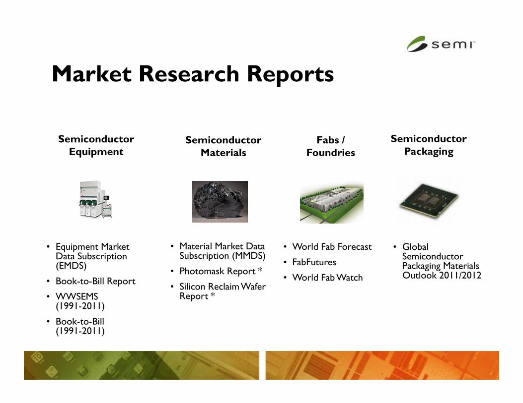
Market Research Reports
Semiconductor Equipment
Semiconductor Materials
• Equipment Market Data Subscription (EMDS)
• Book-to-Bill Report
• WWSEMS(1991-2011)
• Book-to-Bill(1991-2011)
• Material Market Data Subscription (MMDS)
• Photomask Report *
• Silicon Reclaim Wafer Report *
Fabs / Foundries
• World Fab Forecast
• FabFutures
• World Fab Watch
Semiconductor Packaging
• Global Semiconductor Packaging Materials Outlook 2011/2012
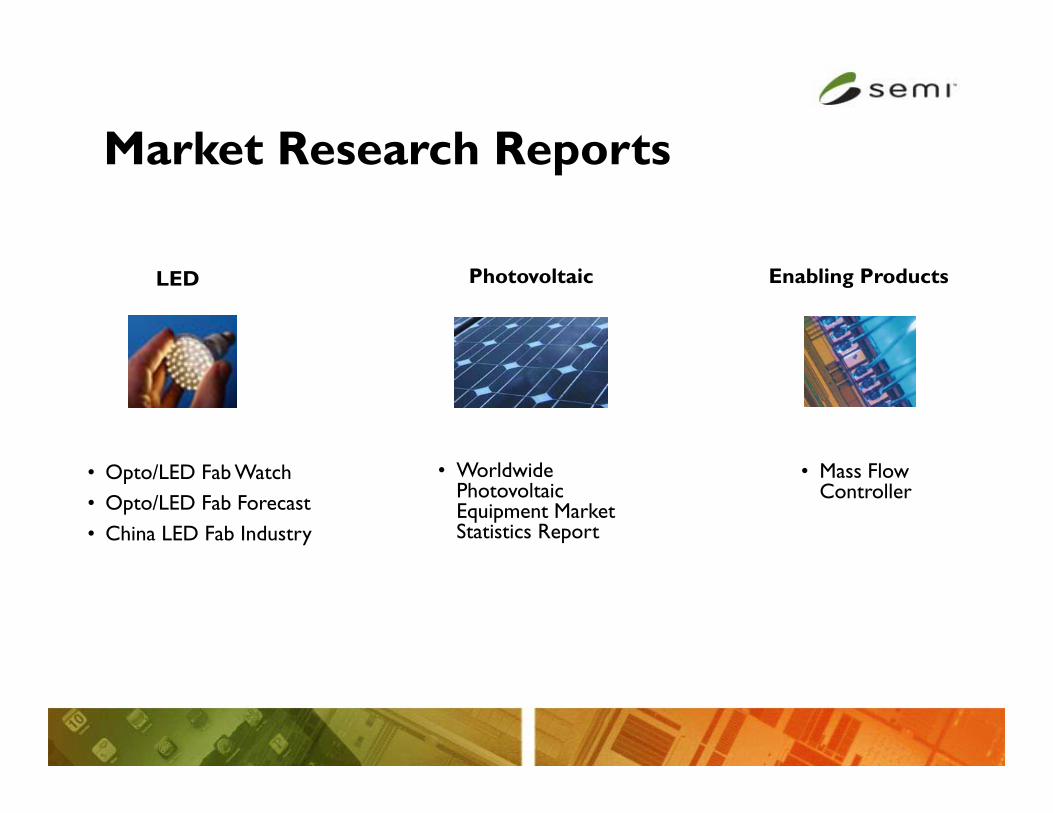
Photovoltaic
• Worldwide Photovoltaic Equipment Market Statistics Report
Enabling Products
• Mass Flow Controller
LED
• Opto/LED Fab Watch• Opto/LED Fab Forecast• China LED Fab Industry
Market Research Reports
SEMI Industry Research and Statistics
Products and data collection programs:
www.semi.org/marketinfo Email: [email protected]
Other Resources
Industry Articles/Press Releases: www.semi.org/marketinfoFab Articles/Interactive Maps: www.semi.org/fabsMarket Research Products: www.semi.org/store
SEMI Member-Only Webinar Archive: www.semi.org/en/node/38101
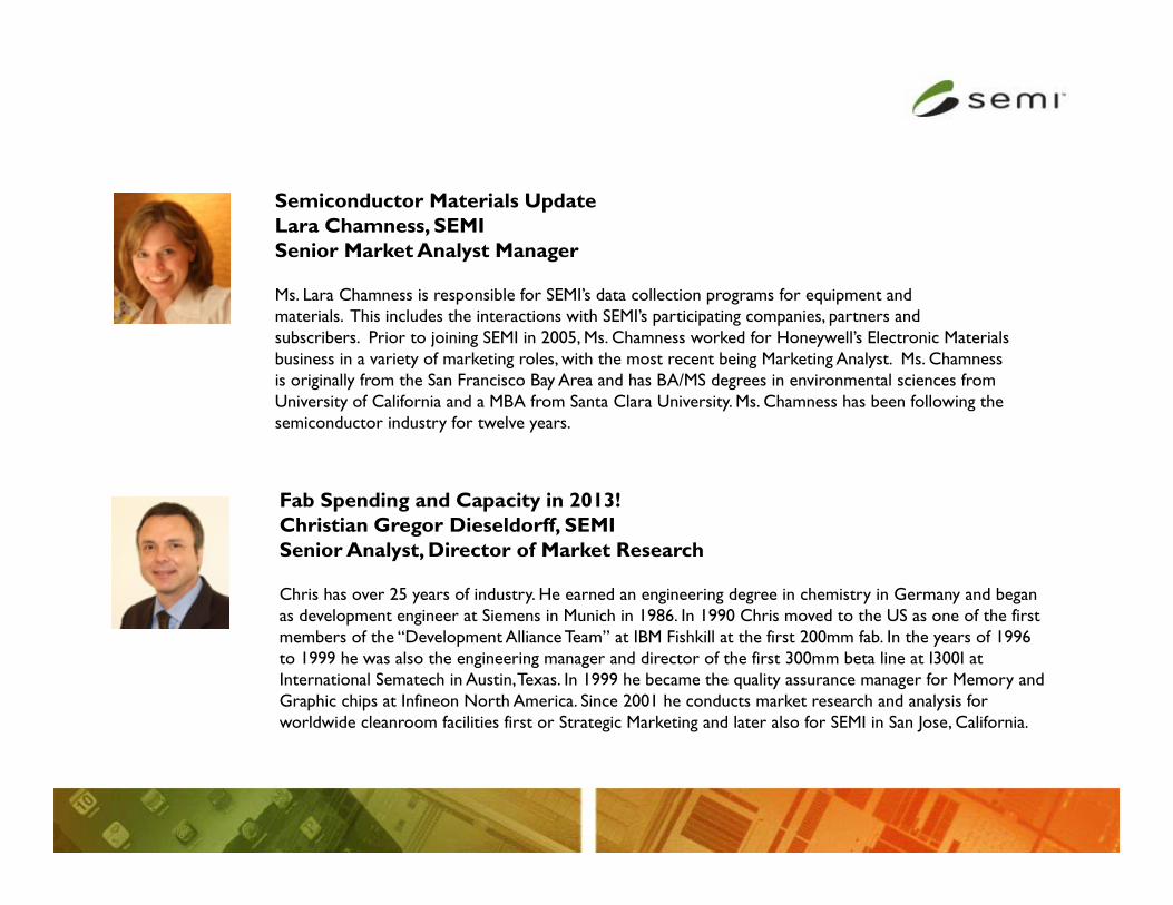
Semiconductor Materials UpdateLara Chamness, SEMISenior Market Analyst Manager
Ms. Lara Chamness is responsible for SEMI’s data collection programs for equipment and materials. This includes the interactions with SEMI’s participating companies, partners and subscribers. Prior to joining SEMI in 2005, Ms. Chamness worked for Honeywell’s Electronic Materials business in a variety of marketing roles, with the most recent being Marketing Analyst. Ms. Chamness is originally from the San Francisco Bay Area and has BA/MS degrees in environmental sciences from University of California and a MBA from Santa Clara University. Ms. Chamness has been following the semiconductor industry for twelve years.
Fab Spending and Capacity in 2013!Christian Gregor Dieseldorff, SEMISenior Analyst, Director of Market Research
Chris has over 25 years of industry. He earned an engineering degree in chemistry in Germany and began as development engineer at Siemens in Munich in 1986. In 1990 Chris moved to the US as one of the first members of the “Development Alliance Team” at IBM Fishkill at the first 200mm fab. In the years of 1996 to 1999 he was also the engineering manager and director of the first 300mm beta line at I300I at International Sematech in Austin, Texas. In 1999 he became the quality assurance manager for Memory and Graphic chips at Infineon North America. Since 2001 he conducts market research and analysis for worldwide cleanroom facilities first or Strategic Marketing and later also for SEMI in San Jose, California.
SEMI Equipment & Materials OutlookLara Chamness, Sr. Market Analyst, Industry Research & Statistics
SEMIDecember 11, 2012
Outline
• Market Trends
• Semiconductor Materials Outlook
• Summary
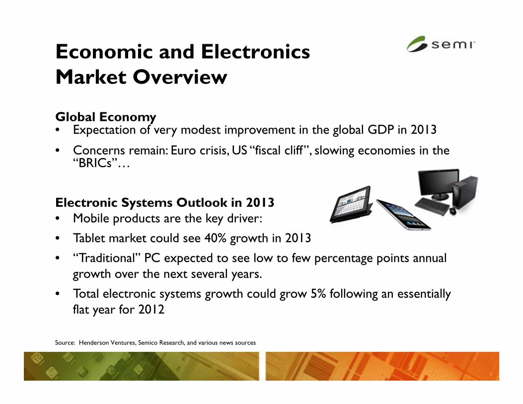
Economic and Electronics Market Overview
Global Economy• Expectation of very modest improvement in the global GDP in 2013
• Concerns remain: Euro crisis, US “fiscal cliff”, slowing economies in the “BRICs”…
Electronic Systems Outlook in 2013• Mobile products are the key driver:
• Tablet market could see 40% growth in 2013
• “Traditional” PC expected to see low to few percentage points annual growth over the next several years.
• Total electronic systems growth could grow 5% following an essentially flat year for 2012
Source: Henderson Ventures, Semico Research, and various news sources
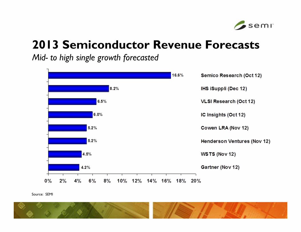
2013 Semiconductor Revenue ForecastsMid- to high single growth forecasted
Source: SEMI
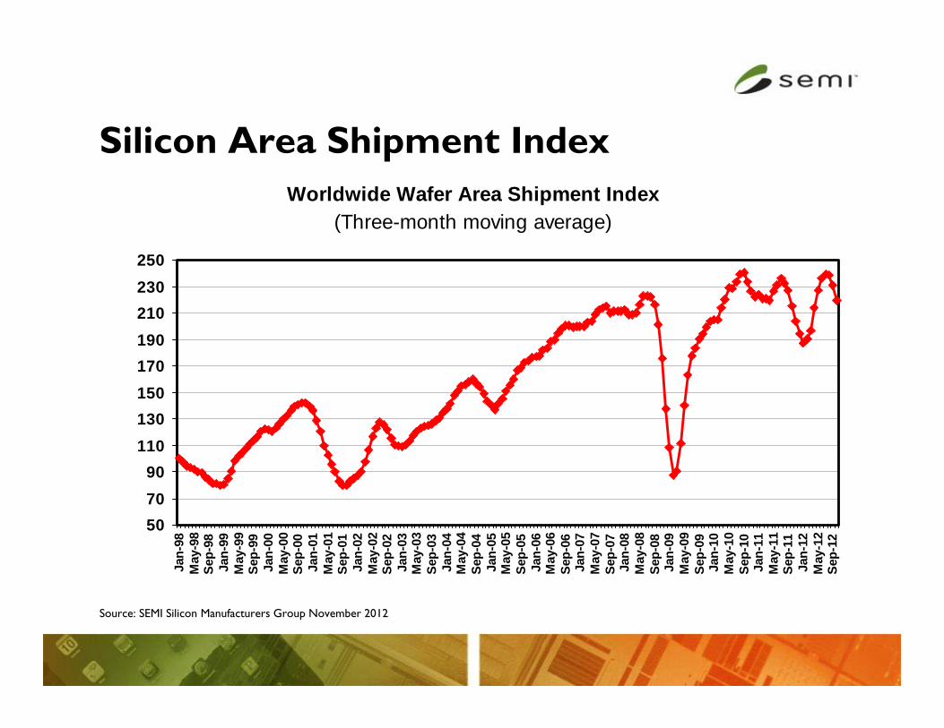
Silicon Area Shipment Index
Source: SEMI Silicon Manufacturers Group November 2012
Worldwide Wafer Area Shipment Index(Three-month moving average)
507090
110130150170190210230250
Jan-
98M
ay-9
8Se
p-98
Jan-
99M
ay-9
9Se
p-99
Jan-
00M
ay-0
0Se
p-00
Jan-
01M
ay-0
1Se
p-01
Jan-
02M
ay-0
2Se
p-02
Jan-
03M
ay-0
3Se
p-03
Jan-
04M
ay-0
4Se
p-04
Jan-
05M
ay-0
5Se
p-05
Jan-
06M
ay-0
6Se
p-06
Jan-
07M
ay-0
7Se
p-07
Jan-
08M
ay-0
8Se
p-08
Jan-
09M
ay-0
9Se
p-09
Jan-
10M
ay-1
0Se
p-10
Jan-
11M
ay-1
1Se
p-11
Jan-
12M
ay-1
2Se
p-12
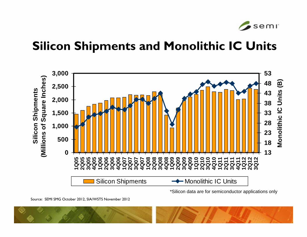
Silicon Shipments and Monolithic IC Units
0
500
1,000
1,500
2,000
2,500
3,0001Q
052Q
053Q
054Q
051Q
062Q
063Q
064Q
061Q
072Q
073Q
074Q
071Q
082Q
083Q
084Q
081Q
092Q
093Q
094Q
091Q
102Q
103Q
104Q
101Q
112Q
113Q
114Q
111Q
122Q
123Q
12
Silic
on S
hipm
ents
(M
illio
ns o
f Squ
are
Inch
es)
131823283338434853
Mon
olith
ic IC
Uni
ts (B
)
Silicon Shipments Monolithic IC Units
Source: SEMI SMG October 2012, SIA/WSTS November 2012
*Silicon data are for semiconductor applications only
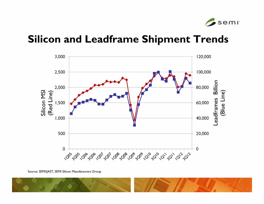
Silicon and Leadframe Shipment Trends
Source: SEMI/JAST, SEMI Silicon Manufacturers Group
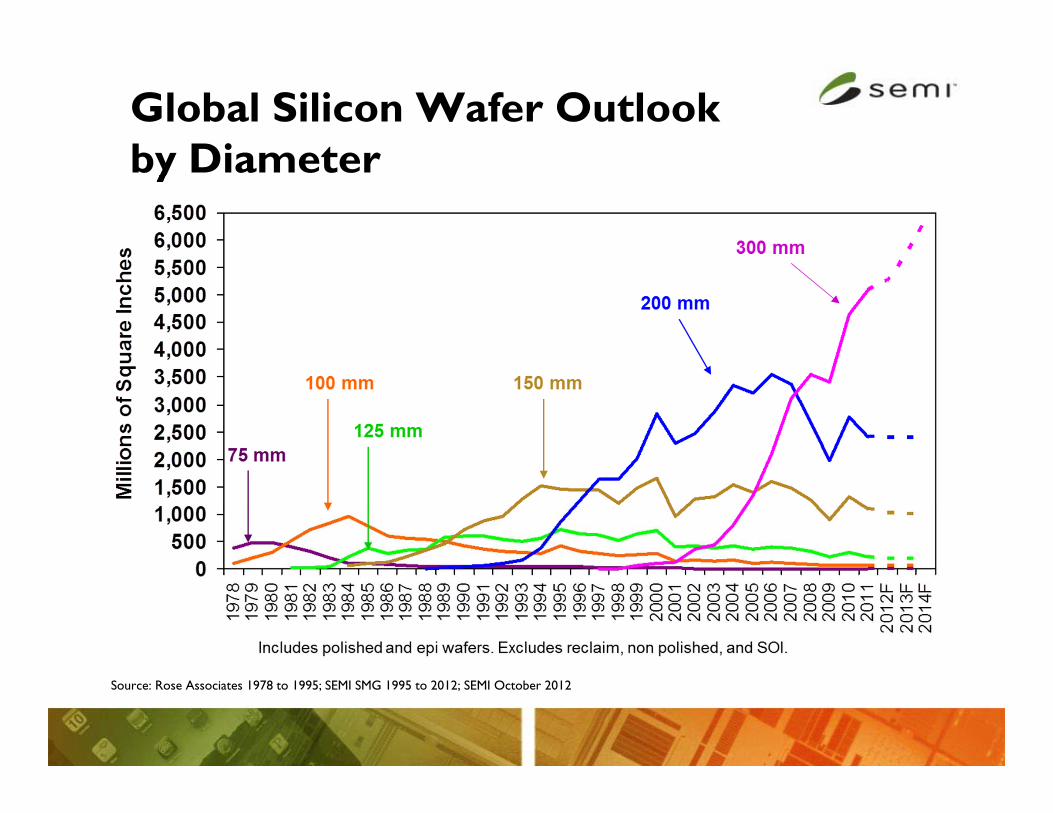
Global Silicon Wafer Outlook by Diameter
Source: Rose Associates 1978 to 1995; SEMI SMG 1995 to 2012; SEMI October 2012
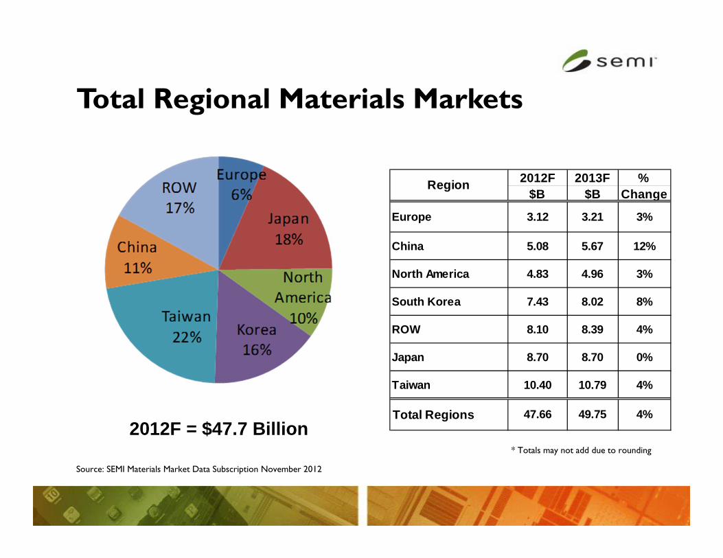
Total Regional Materials Markets
* Totals may not add due to rounding
2012F = $47.7 Billion
2012F 2013F %$B $B Change
Europe 3.12 3.21 3%
China 5.08 5.67 12%
North America 4.83 4.96 3%
South Korea 7.43 8.02 8%
ROW 8.10 8.39 4%
Japan 8.70 8.70 0%
Taiwan 10.40 10.79 4%
Total Regions 47.66 49.75 4%
Region
Source: SEMI Materials Market Data Subscription November 2012
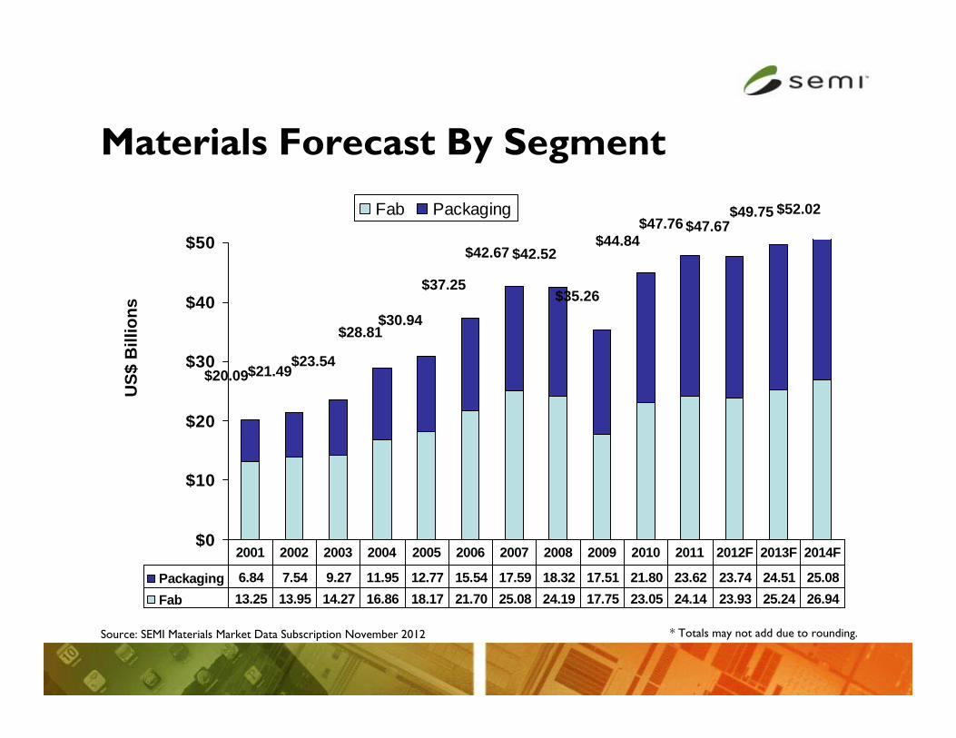
Materials Forecast By Segment
$0
$10
$20
$30
$40
$50
Fab Packaging
Packaging 6.84 7.54 9.27 11.95 12.77 15.54 17.59 18.32 17.51 21.80 23.62 23.74 24.51 25.08Fab 13.25 13.95 14.27 16.86 18.17 21.70 25.08 24.19 17.75 23.05 24.14 23.93 25.24 26.94
2001 2002 2003 2004 2005 2006 2007 2008 2009 2010 2011 2012F 2013F 2014F
US$
Bill
ions
* Totals may not add due to rounding.
$28.81$30.94
$42.67 $42.52
$35.26
$44.84
$37.25
Source: SEMI Materials Market Data Subscription November 2012
$47.76
$23.54$21.49$20.09
$49.75$47.67
$52.02
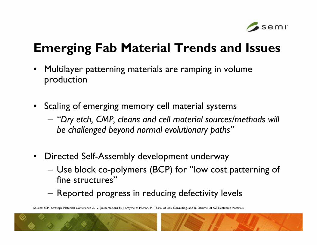
Emerging Fab Material Trends and Issues
• Multilayer patterning materials are ramping in volume production
• Scaling of emerging memory cell material systems– “Dry etch, CMP, cleans and cell material sources/methods will
be challenged beyond normal evolutionary paths”
• Directed Self-Assembly development underway– Use block co-polymers (BCP) for “low cost patterning of
fine structures”– Reported progress in reducing defectivity levels
Source: SEMI Strategic Materials Conference 2012 (presentations by J. Smythe of Micron, M. Thirsk of Linx Consulting, and R. Dammel of AZ Electronic Materials
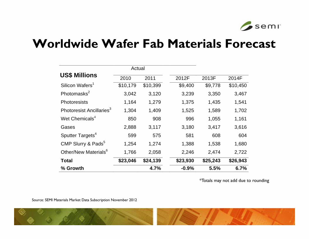
Worldwide Wafer Fab Materials Forecast
Source: SEMI Materials Market Data Subscription November 2012
Actual
2010 2011 2012F 2013F 2014F Silicon Wafers1 $10,179 $10,399 $9,400 $9,778 $10,450
Photomasks2 3,042 3,120 3,239 3,350 3,467
Photoresists 1,164 1,279 1,375 1,435 1,541
Photoresist Ancillaries3 1,304 1,409 1,525 1,589 1,702
Wet Chemicals4 850 908 996 1,055 1,161
Gases 2,888 3,117 3,180 3,417 3,616
Sputter Targets4 599 575 581 608 604
CMP Slurry & Pads5 1,254 1,274 1,388 1,538 1,680
Other/New Materials6 1,766 2,058 2,246 2,474 2,722
Total $23,046 $24,139 $23,930 $25,243 $26,943% Growth 4.7% -0.9% 5.5% 6.7%
US$ Millions
*Totals may not add due to rounding
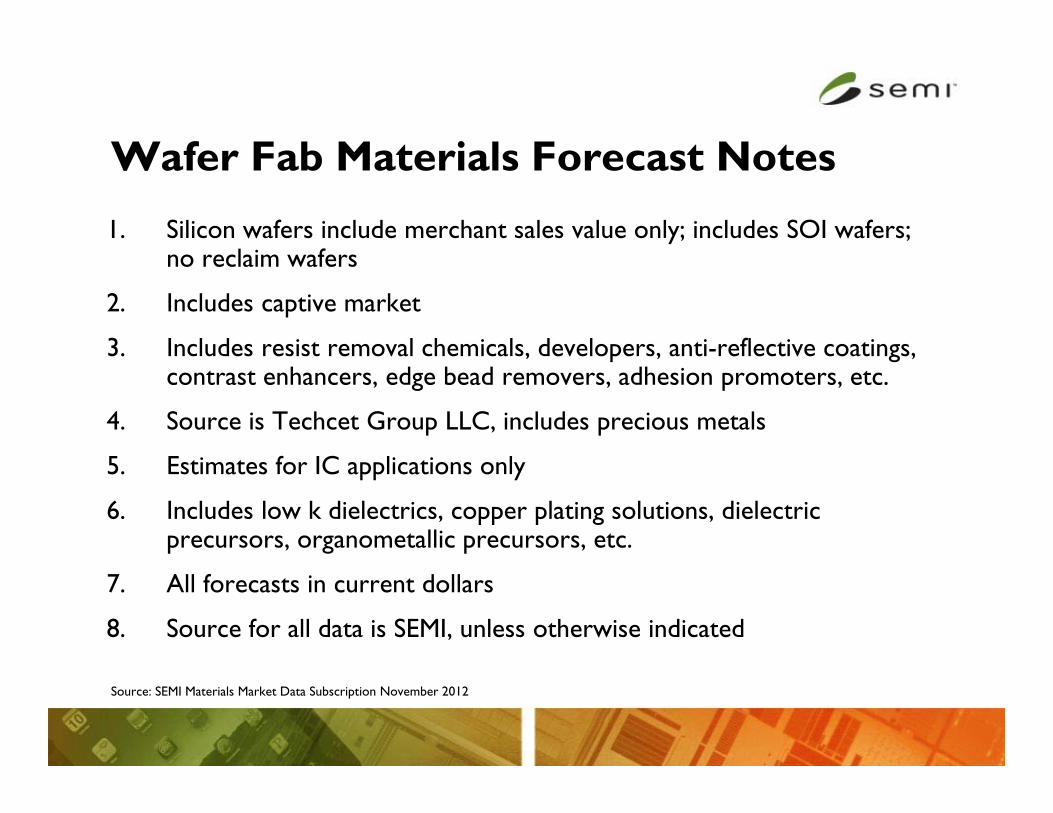
Wafer Fab Materials Forecast Notes
1. Silicon wafers include merchant sales value only; includes SOI wafers; no reclaim wafers
2. Includes captive market
3. Includes resist removal chemicals, developers, anti-reflective coatings, contrast enhancers, edge bead removers, adhesion promoters, etc.
4. Source is Techcet Group LLC, includes precious metals
5. Estimates for IC applications only
6. Includes low k dielectrics, copper plating solutions, dielectric precursors, organometallic precursors, etc.
7. All forecasts in current dollars
8. Source for all data is SEMI, unless otherwise indicated
Source: SEMI Materials Market Data Subscription November 2012
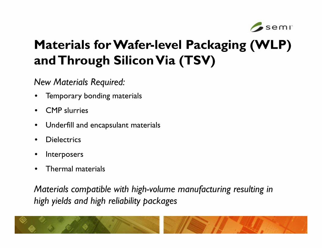
Materials for Wafer-level Packaging (WLP) and Through Silicon Via (TSV)
• Temporary bonding materials
• CMP slurries
• Underfill and encapsulant materials
• Dielectrics
• Interposers
• Thermal materials
Materials compatible with high-volume manufacturing resulting in high yields and high reliability packages
New Materials Required:
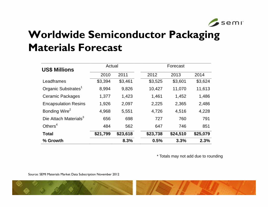
Worldwide Semiconductor PackagingMaterials Forecast
Actual Forecast
2010 2011 2012 2013 2014 Leadframes $3,394 $3,461 $3,525 $3,601 $3,624
Organic Substrates1 8,994 9,826 10,427 11,070 11,613
Ceramic Packages 1,377 1,423 1,461 1,452 1,486
Encapsulation Resins 1,926 2,097 2,225 2,365 2,486
Bonding Wire2 4,968 5,551 4,726 4,516 4,228
Die Attach Materials3 656 698 727 760 791
Others4 484 562 647 746 851
Total $21,799 $23,618 $23,738 $24,510 $25,079% Growth 8.3% 0.5% 3.3% 2.3%
Source: SEMI Materials Market Data Subscription November 2012
US$ Millions
* Totals may not add due to rounding
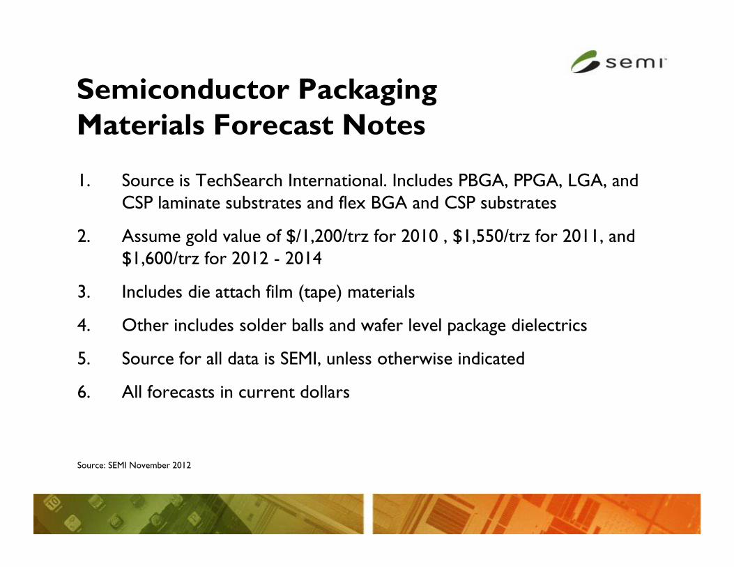
Semiconductor Packaging Materials Forecast Notes
1. Source is TechSearch International. Includes PBGA, PPGA, LGA, and CSP laminate substrates and flex BGA and CSP substrates
2. Assume gold value of $/1,200/trz for 2010 , $1,550/trz for 2011, and $1,600/trz for 2012 - 2014
3. Includes die attach film (tape) materials
4. Other includes solder balls and wafer level package dielectrics
5. Source for all data is SEMI, unless otherwise indicated
6. All forecasts in current dollars
Source: SEMI November 2012
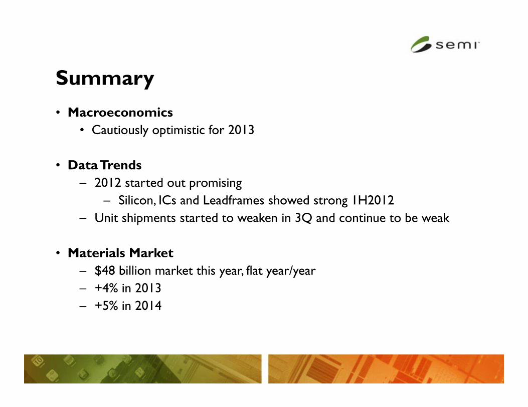
Summary
• Macroeconomics• Cautiously optimistic for 2013
• Data Trends– 2012 started out promising
– Silicon, ICs and Leadframes showed strong 1H2012– Unit shipments started to weaken in 3Q and continue to be weak
• Materials Market– $48 billion market this year, flat year/year– +4% in 2013– +5% in 2014
Acknowledgements
• Dan Tracy, Senior Director Industry Research and Statistics, SEMI
• Lita Shon-Roy, Sr. Managing Partner, Techcet Group, LLC.
Fab Spending and Capacity in 2013
SEMI Webinar: Outlook on the Semiconductor Manufacturing IndustryC.G. Dieseldorff, Senior Analyst
Industry Research & Statistics Group at SEMI
December 11, 2012
December 11, 2012 C.G. Dieseldorff, SEMI San Jose 27
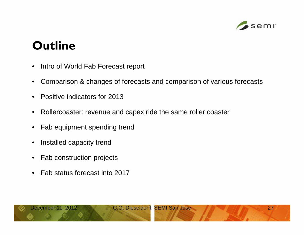
Outline
• Intro of World Fab Forecast report
• Comparison & changes of forecasts and comparison of various forecasts
• Positive indicators for 2013
• Rollercoaster: revenue and capex ride the same roller coaster
• Fab equipment spending trend
• Installed capacity trend
• Fab construction projects
• Fab status forecast into 2017
World Fab Forecast Report
December 11, 2012 C.G. Dieseldorff, SEMI San Jose 28
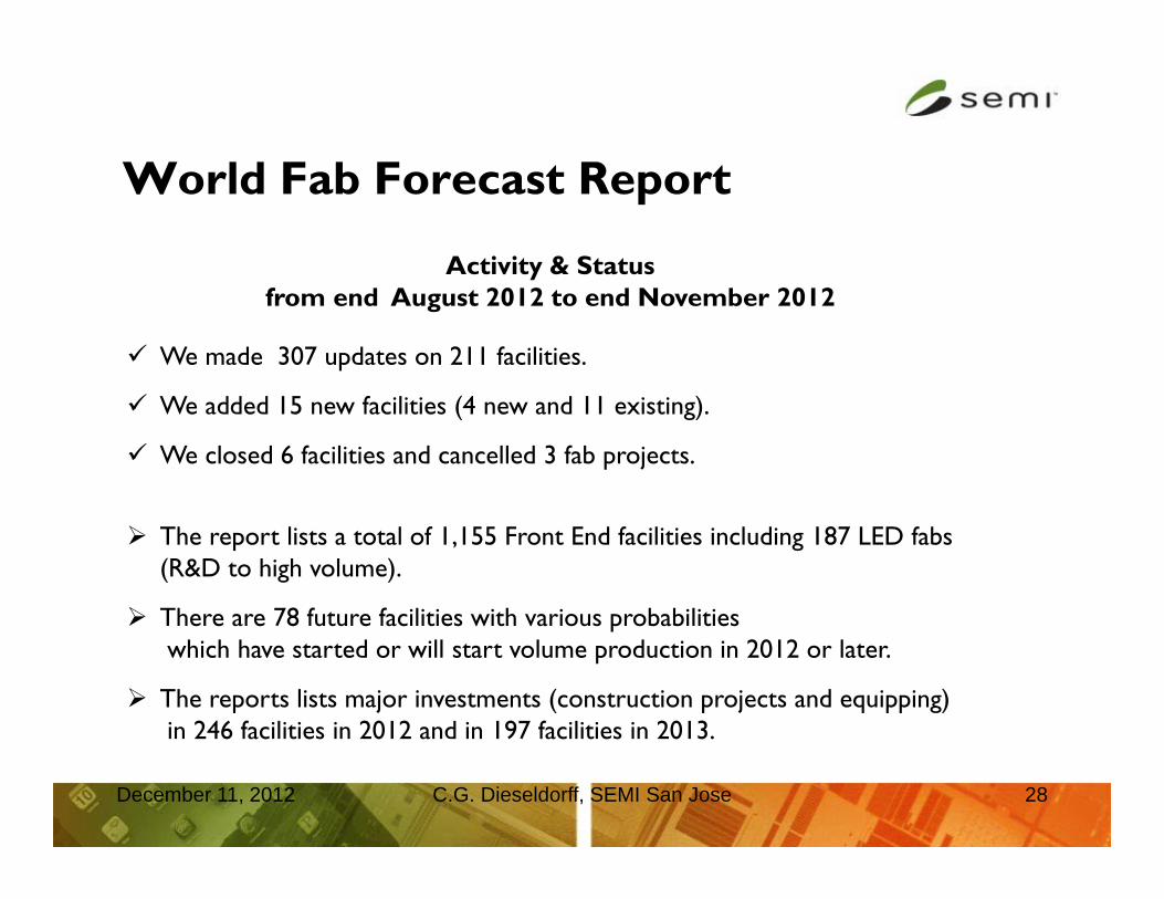
Activity & Statusfrom end August 2012 to end November 2012
We made 307 updates on 211 facilities.
We added 15 new facilities (4 new and 11 existing).
We closed 6 facilities and cancelled 3 fab projects.
The report lists a total of 1,155 Front End facilities including 187 LED fabs(R&D to high volume).
There are 78 future facilities with various probabilitieswhich have started or will start volume production in 2012 or later.
The reports lists major investments (construction projects and equipping)in 246 facilities in 2012 and in 197 facilities in 2013.
December 11, 2012 C.G. Dieseldorff, SEMI San Jose 29
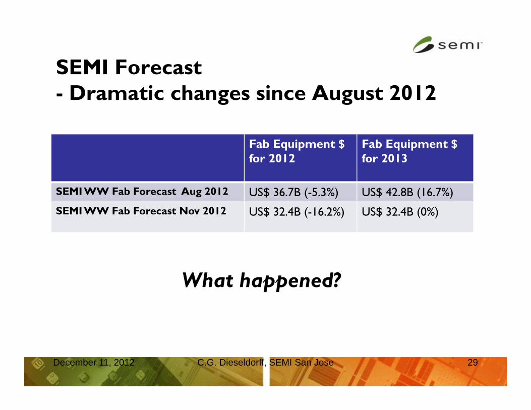
Fab Equipment $for 2012
Fab Equipment $for 2013
SEMI WW Fab Forecast Aug 2012 US$ 36.7B (-5.3%) US$ 42.8B (16.7%)
SEMI WW Fab Forecast Nov 2012 US$ 32.4B (-16.2%) US$ 32.4B (0%)
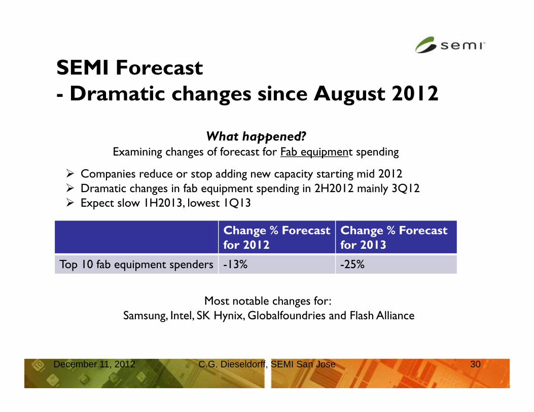
What happened?
SEMI Forecast- Dramatic changes since August 2012
December 11, 2012 C.G. Dieseldorff, SEMI San Jose 30
What happened?Examining changes of forecast for Fab equipment spending
Companies reduce or stop adding new capacity starting mid 2012 Dramatic changes in fab equipment spending in 2H2012 mainly 3Q12 Expect slow 1H2013, lowest 1Q13
Change % Forecast for 2012
Change % Forecast for 2013
Top 10 fab equipment spenders -13% -25%
Most notable changes for: Samsung, Intel, SK Hynix, Globalfoundries and Flash Alliance
SEMI Forecast- Dramatic changes since August 2012
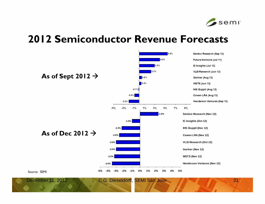
2012 Semiconductor Revenue Forecasts
December 11, 2012 C.G. Dieseldorff, SEMI San Jose 31
Source: SEMI
-3.2%
-3.0%
-3.0%
-2.6%
-2.3%
-1.0%
2.3%
-3.5%
-5% -4% -3% -2% -1% 0% 1% 2% 3% 4% 5%
Henderson Ventures (Nov 12)
WSTS (Nov 12)
Gartner (Nov 12)
VLSI Research (Oct 12)
Cowen LRA (Nov 12)
IHS iSuppli (Dec 12)
IC Insights (Oct 12)
Semico Research (Nov 12)
As of Sept 2012
As of Dec 2012
December 11, 2012 C.G. Dieseldorff, SEMI San Jose 32
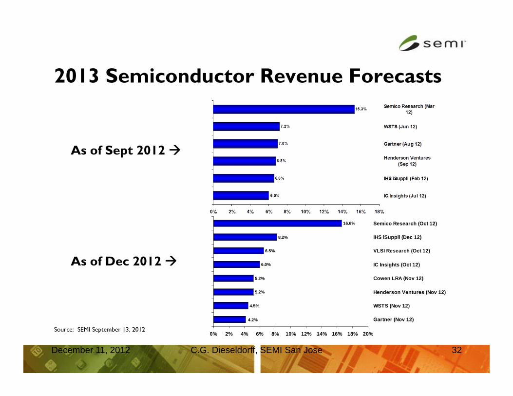
Source: SEMI September 13, 2012
4.5%
5.2%
5.2%
6.0%
6.5%
8.2%
16.6%
4.2%
0% 2% 4% 6% 8% 10% 12% 14% 16% 18% 20%
Gartner (Nov 12)
WSTS (Nov 12)
Henderson Ventures (Nov 12)
Cowen LRA (Nov 12)
IC Insights (Oct 12)
VLSI Research (Oct 12)
IHS iSuppli (Dec 12)
Semico Research (Oct 12)
As of Sept 2012
As of Dec 2012
2013 Semiconductor Revenue Forecasts
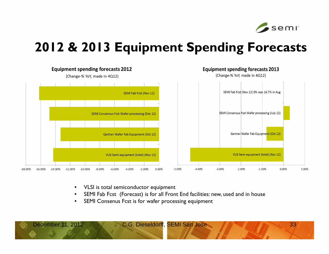
2012 & 2013 Equipment Spending Forecasts
December 11, 2012 C.G. Dieseldorff, SEMI San Jose 33
• VLSI is total semiconductor equipment• SEMI Fab Fcst (Forecast) is for all Front End facilities: new, used and in house• SEMI Consenus Fcst is for wafer processing equipment
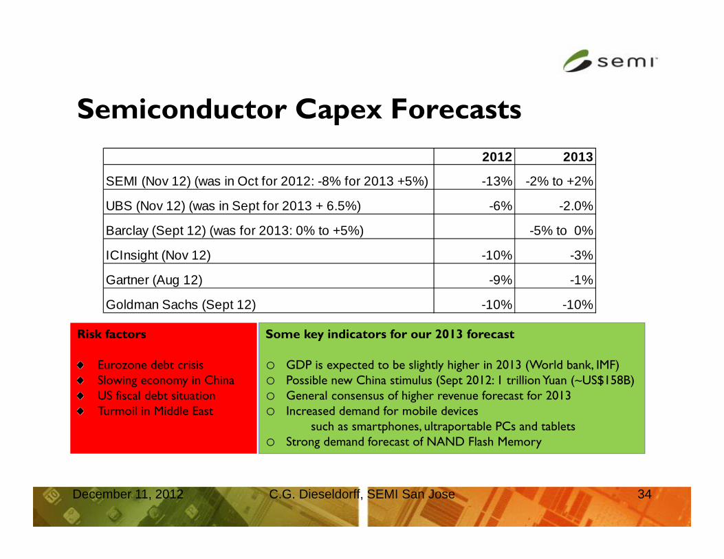
Semiconductor Capex Forecasts
December 11, 2012 C.G. Dieseldorff, SEMI San Jose 34
Some key indicators for our 2013 forecast
o GDP is expected to be slightly higher in 2013 (World bank, IMF)o Possible new China stimulus (Sept 2012: 1 trillion Yuan (~US$158B)o General consensus of higher revenue forecast for 2013o Increased demand for mobile devices
such as smartphones, ultraportable PCs and tabletso Strong demand forecast of NAND Flash Memory
Risk factors
Eurozone debt crisisSlowing economy in ChinaUS fiscal debt situationTurmoil in Middle East
2012 2013
SEMI (Nov 12) (was in Oct for 2012: -8% for 2013 +5%) -13% -2% to +2%
UBS (Nov 12) (was in Sept for 2013 + 6.5%) -6% -2.0%
Barclay (Sept 12) (was for 2013: 0% to +5%) -5% to 0%
ICInsight (Nov 12) -10% -3%
Gartner (Aug 12) -9% -1%
Goldman Sachs (Sept 12) -10% -10%
December 11, 2012 C.G. Dieseldorff, SEMI San Jose 35
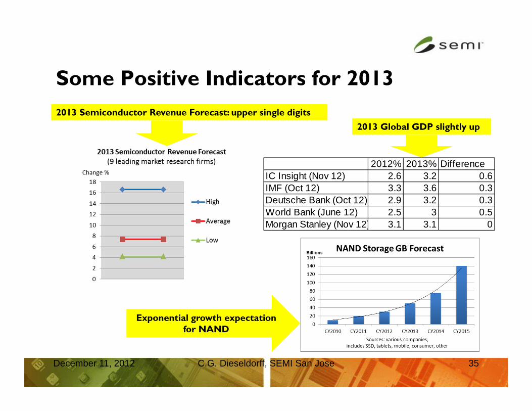
Some Positive Indicators for 2013
2013 Global GDP slightly up
2012% 2013% DifferenceIC Insight (Nov 12) 2.6 3.2 0.6IMF (Oct 12) 3.3 3.6 0.3Deutsche Bank (Oct 12) 2.9 3.2 0.3World Bank (June 12) 2.5 3 0.5Morgan Stanley (Nov 12) 3.1 3.1 0
2013 Semiconductor Revenue Forecast: upper single digits
Exponential growth expectation for NAND
December 11, 2012 C.G. Dieseldorff, SEMI San Jose 36
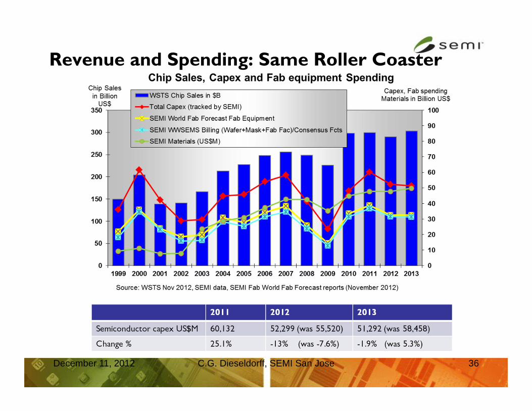
Revenue and Spending: Same Roller Coaster
Fab Equipment Spending
December 11, 2012 C.G. Dieseldorff, SEMI San Jose 37
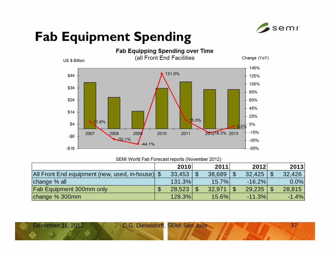
2010 2011 2012 2013All Front End equipment (new, used, in-house) 33,453$ 38,689$ 32,425$ 32,426$ change % all 131.3% 15.7% -16.2% 0.0%Fab Equipment 300mm only 28,523$ 32,971$ 29,235$ 28,815$ change % 300mm 128.3% 15.6% -11.3% -1.4%
Fab Equipment Spending
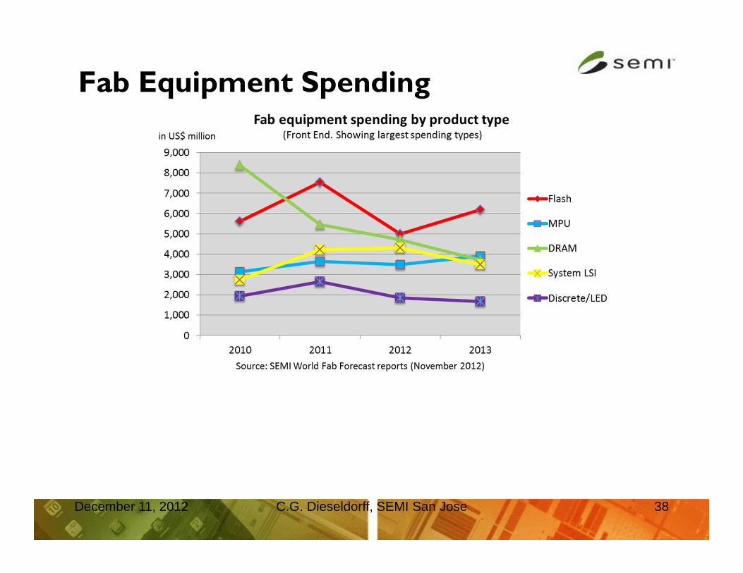
December 11, 2012 C.G. Dieseldorff, SEMI San Jose 38
Fab Equipment Spending Versus Capacity
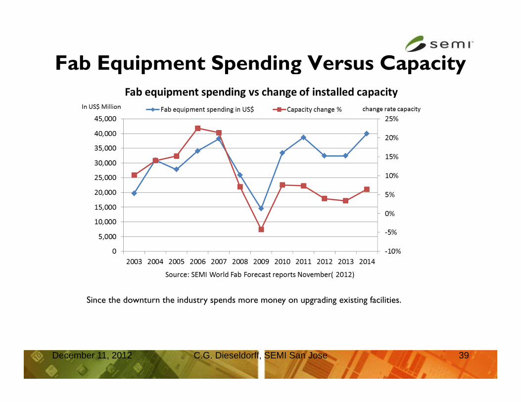
December 11, 2012 C.G. Dieseldorff, SEMI San Jose 39
Since the downturn the industry spends more money on upgrading existing facilities.
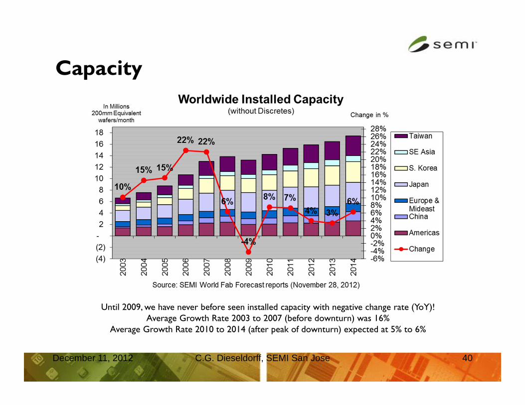
Capacity
December 11, 2012 C.G. Dieseldorff, SEMI San Jose 40
Until 2009, we have never before seen installed capacity with negative change rate (YoY)!Average Growth Rate 2003 to 2007 (before downturn) was 16%
Average Growth Rate 2010 to 2014 (after peak of downturn) expected at 5% to 6%
December 11, 2012 C.G. Dieseldorff, SEMI San Jose 41
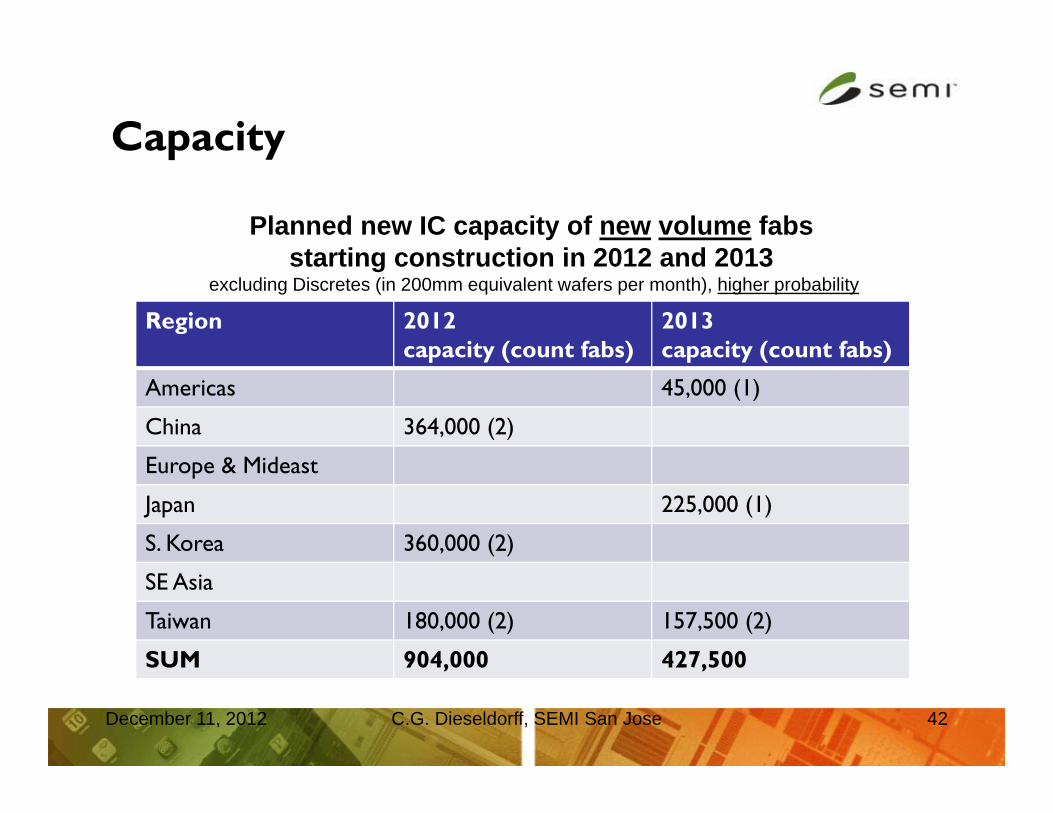
Capacity
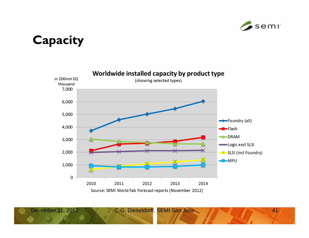
December 11, 2012 C.G. Dieseldorff, SEMI San Jose 42
Planned new IC capacity of new volume fabs starting construction in 2012 and 2013
excluding Discretes (in 200mm equivalent wafers per month), higher probability
Region 2012capacity (count fabs)
2013capacity (count fabs)
Americas 45,000 (1)
China 364,000 (2)
Europe & Mideast
Japan 225,000 (1)
S. Korea 360,000 (2)
SE Asia
Taiwan 180,000 (2) 157,500 (2)
SUM 904,000 427,500
Capacity
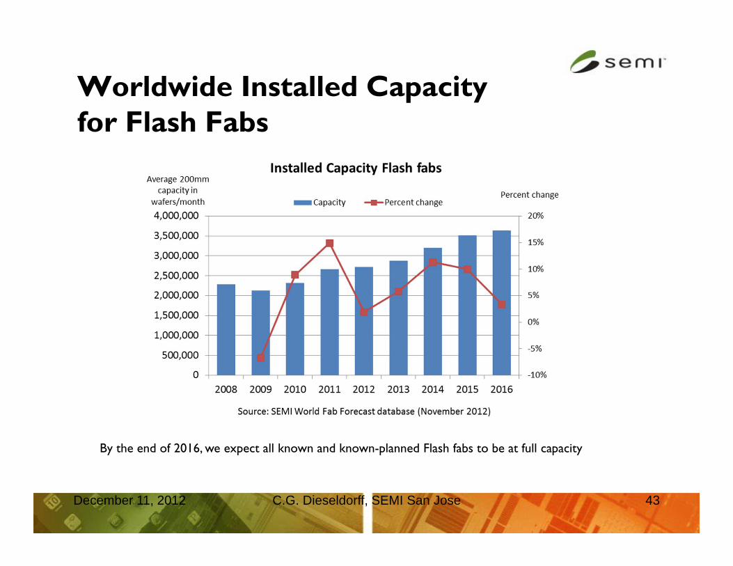
Worldwide Installed Capacity for Flash Fabs
December 11, 2012 C.G. Dieseldorff, SEMI San Jose 43
By the end of 2016, we expect all known and known-planned Flash fabs to be at full capacity
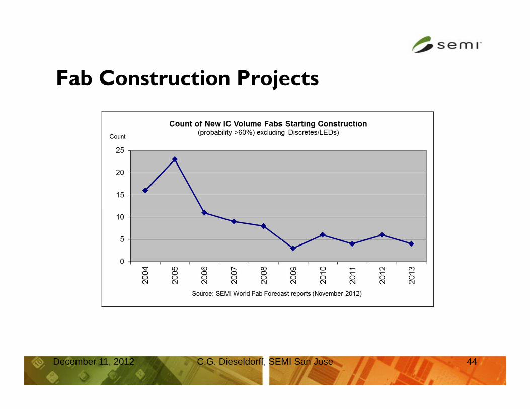
Fab Construction Projects
December 11, 2012 C.G. Dieseldorff, SEMI San Jose 44
December 11, 2012 C.G. Dieseldorff, SEMI San Jose 45
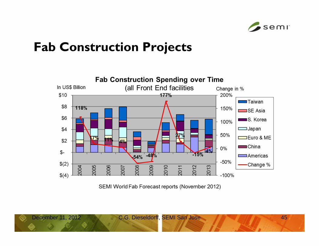
Fab Construction Projects
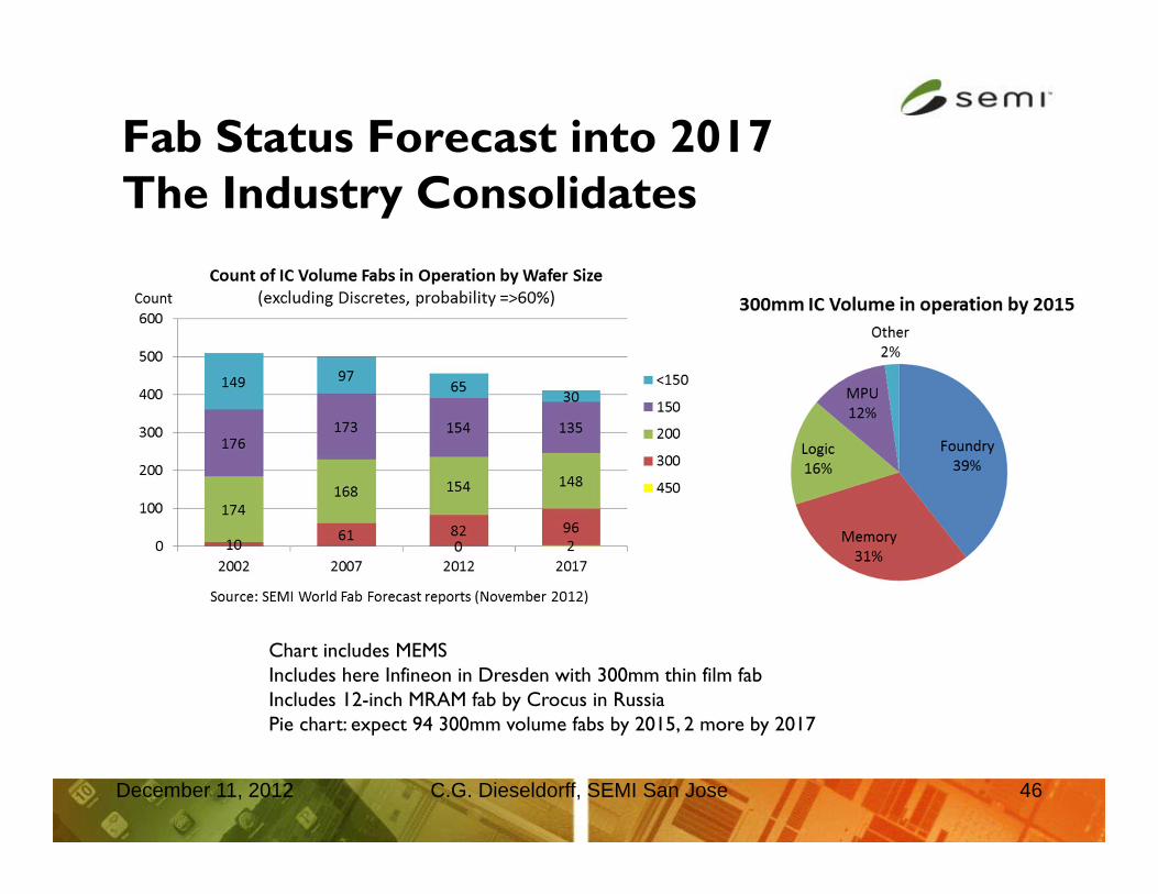
Fab Status Forecast into 2017The Industry Consolidates
December 11, 2012 C.G. Dieseldorff, SEMI San Jose 46
Chart includes MEMSIncludes here Infineon in Dresden with 300mm thin film fabIncludes 12-inch MRAM fab by Crocus in RussiaPie chart: expect 94 300mm volume fabs by 2015, 2 more by 2017
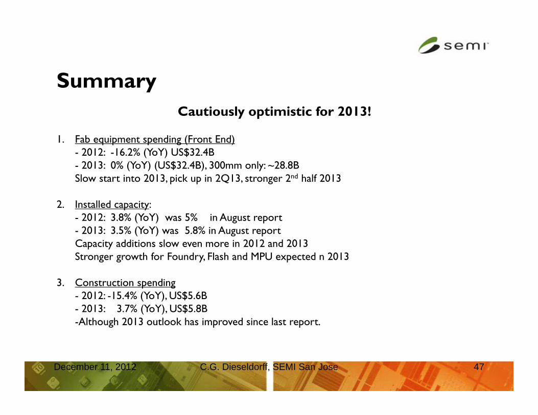
Summary
1. Fab equipment spending (Front End) - 2012: -16.2% (YoY) US$32.4B- 2013: 0% (YoY) (US$32.4B), 300mm only: ~28.8BSlow start into 2013, pick up in 2Q13, stronger 2nd half 2013
2. Installed capacity:- 2012: 3.8% (YoY) was 5% in August report- 2013: 3.5% (YoY) was 5.8% in August reportCapacity additions slow even more in 2012 and 2013Stronger growth for Foundry, Flash and MPU expected n 2013
3. Construction spending- 2012: -15.4% (YoY), US$5.6B - 2013: 3.7% (YoY), US$5.8B-Although 2013 outlook has improved since last report.
C.G. Dieseldorff, SEMI San Jose 47December 11, 2012
Cautiously optimistic for 2013!
SEMI Industry Research and Statistics
Products and data collection programs:www.semi.org/marketinfo
Contact: Ed Hall: [email protected] or [email protected]
Other ResourcesIndustry Articles/Press Releases: www.semi.org/marketinfo
Fab Articles/Interactive Maps: www.semi.org/fabsMarket Research Products: www.semi.org/store
SEMI Member-Only Webinar Archive: www.semi.org/en/node/38101Twitter: www.twitter.com/SEMI_mktstatsSlideshare: www.slideshare.net/ehallSEMI
YouTube: www.youtube.com/user/SEMImktstats
Thank You!
• Questions?
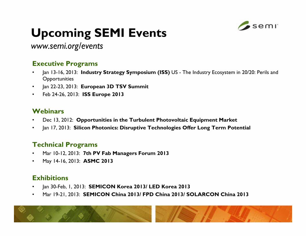
Upcoming SEMI Eventswww.semi.org/events
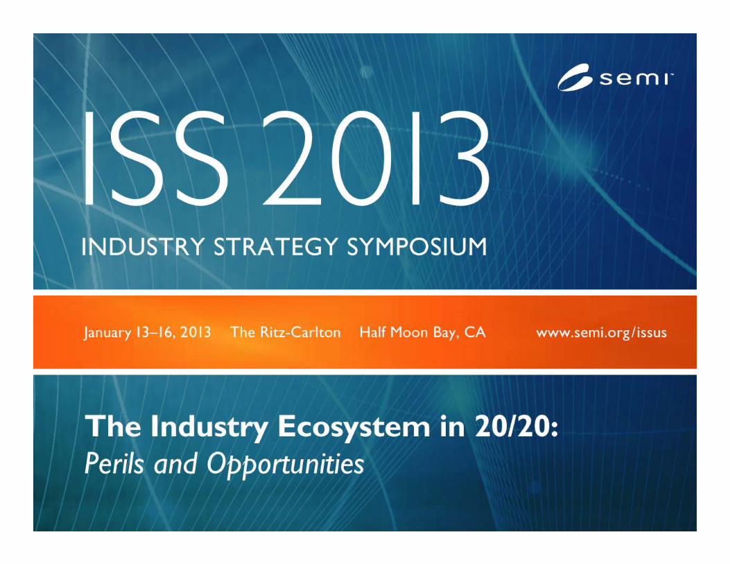
Executive Programs• Jan 13-16, 2013: Industry Strategy Symposium (ISS) US - The Industry Ecosystem in 20/20: Perils and
Opportunities • Jan 22-23, 2013: European 3D TSV Summit• Feb 24-26, 2013: ISS Europe 2013
Webinars• Dec 13, 2012: Opportunities in the Turbulent Photovoltaic Equipment Market• Jan 17, 2013: Silicon Photonics: Disruptive Technologies Offer Long Term Potential
Technical Programs• Mar 10-12, 2013: 7th PV Fab Managers Forum 2013• May 14-16, 2013: ASMC 2013
Exhibitions• Jan 30-Feb, 1, 2013: SEMICON Korea 2013/ LED Korea 2013• Mar 19-21, 2013: SEMICON China 2013/ FPD China 2013/ SOLARCON China 2013
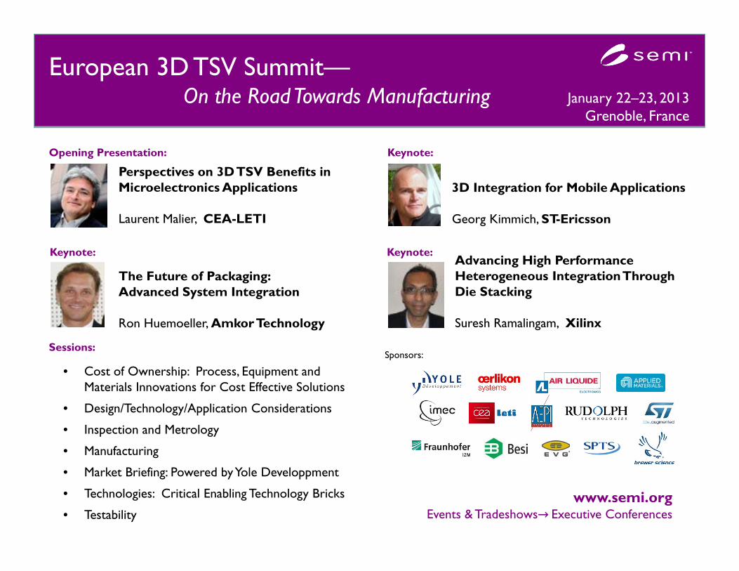
Perspectives on 3D TSV Benefits in Microelectronics Applications
Laurent Malier, CEA-LETI
3D Integration for Mobile Applications
Georg Kimmich, ST-Ericsson
Opening Presentation:
The Future of Packaging: Advanced System Integration
Ron Huemoeller, Amkor Technology
Advancing High Performance Heterogeneous Integration Through Die Stacking
Suresh Ramalingam, Xilinx
Keynote: Keynote:
Keynote:
Sessions:
• Cost of Ownership: Process, Equipment andMaterials Innovations for Cost Effective Solutions
• Design/Technology/Application Considerations
• Inspection and Metrology
• Manufacturing
• Market Briefing: Powered by Yole Developpment
• Technologies: Critical Enabling Technology Bricks
• Testabilitywww.semi.org
Events & Tradeshows→Executive Conferences
European 3D TSV Summit—On the Road Towards Manufacturing January 22–23, 2013
Grenoble, France
Sponsors:

Harnessing European Innovation for the Global Market
Join us at ISS Europe 2013February 24–26
Milan, Italy
www.semi.org/isseurope
Sponsors: Logo Sponsors:
End of Webinar
54December 11, 2012
Backup slides
C.G. Dieseldorff, SEMI San Jose 55December 11, 2012
December 11, 2012 C.G. Dieseldorff, SEMI San Jose 56
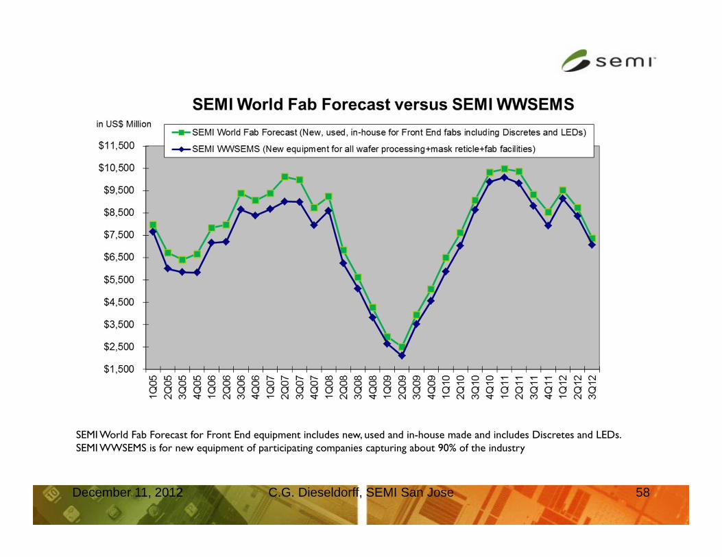
Difference SEMI’s WWSEMS to SEMI’s World Fab Forecast
SEMI’s Worldwide Semiconductor Equipment Market Subscription (WWSEMS) data tracks only new equipment for fabs and test and assembly and packaging houses. This survey done by a third party covers about 90% of the industry's equipment suppliers.
The SEMI World Fab Forecast and its related Fab Database reports track anyequipment needed to ramp Front End facilities, upgrade technology nodes, and expand or change wafer size, including new equipment, used equipment, or in-house equipment. The report covers from small R&D to high volume fabs and includes Discretes and LEDs.
If we compare the equipment data between WWSEMS and Fab database, we are including wafer processing equipment, mask & reticle, and Fab facilities of WWSEMS and compare with Fab database equipment data.
December 11, 2012 C.G. Dieseldorff, SEMI San Jose 57
Definition of SEMI Consensus Forecast
SEMI has a long tradition of generating “Consensus Forecasts” for new semiconductor equipment. These forecasts are published two times a year in conjunction with SEMICON West in July and SEMICON Japan in December.
The intent of these forecasts is to provide a gauge of member sentiment for market conditions. SEMI bases this forecast on monthly “bookings and billings” data that it collects directly from semiconductor equipment suppliers, data from the SEMI World Fab database, and feedback from equipment suppliers.
The “Consensus Forecast” covers both “Front-end” equipment (typically associated with wafer fabrication) and “Back-end” equipment (equipment used to package and test individual devices).
The “Consensus Forecast” contrasts to the “bottoms-up” forecast generated by the World Fab database, which bases its projections on CapEx announcements by device manufacturers and only covers fab equipment, including used and equipment manufactured directly by fabs.
December 11, 2012 C.G. Dieseldorff, SEMI San Jose 58
SEMI World Fab Forecast for Front End equipment includes new, used and in-house made and includes Discretes and LEDs.SEMI WWSEMS is for new equipment of participating companies capturing about 90% of the industry