wd1002·05! h do winchester! floppy disk controller oem …€¦ · h do winchester! floppy disk...
TRANSCRIPT
PRELIMINARY
WD1002·05! H DO
Winchester! Floppy Disk
Controller
OEM Manual
Document No.: 61·031050·0030
IIIIESTERN DIGITAL COR PO RAT ION
2445 McCabe Way Irvine, California 92714
(714) 863-0102 TWX 910-595-1139
July 1983
SECTION 1
SECTION 2
SECTION 3
SECTION 4
TABLE OF CONTENTS
INTRODUCTION
1.1 Description............................................................ 1-1 1.1.1 On-Board Processing and Control Devices ............................... 1-1 1.1.2 Communications Between Host and WD1002-05 .......................... 1-2
1.2 Specifications.......................................................... 1-3 1.2.1 Performance....................................................... 1-3 1.2.2 Physical .......................................................... 1-3 1.2.3 Environmental ............................................. : ....... 1-3
INTERFACE CONNECTORS
2.1 Organization........................................................... 2-1 2.2 Host Interface Connector Signals. . . . . . . . . . . . . . . . . . . . . . . . . . . . . . . . . . . . . . . . . . . 2-1 2.3 4O-Pin Host Interface Connector ............................................ 2-1 2.4 Winchester Drive Control Signals . . . . . . . . . . . . . . . . . . . . . . . . . . . . . . . . . . . . . . . . . . . 2-1 2.5 5.25" Winchester 34-Pin Drive Control Connector .............................. 2-2 2.6 Winchester Drive Data Connector. . . . . . . . . . . . . . . . . . . . . . . . . . . . . . . . . . . . . . . . . . . 2-2 2.7 Power Con nector . . . . . . . . . . . . . . . . . . . . . . . . . . . . . . . . . . . . . . . . . . . . . . . . . . . . . . . . 2-3 2.8 Floppy Drive Signals .. . . . . . . . . . . . . . . . . . . . . . . . . . . . . . . . . . . . . . . . . . . . . . . . . . . . 2-3 2.9 5.25" Floppy 34-Pin Drive Control Connector . . . . . . . . . . . . . . . . . . . . . . . . . . . . . . . . . . 2-4
INTERFACE TIMING
3.1 HostlnterfaceTiming .................................................... 3-1 3.1.1 Host Task File Read Timing ........................................... 3-1 3.1.2 Host Task File Write Timing .............................. ; . . . . . . . . . . . . 3-1 3.1.3 Host Sector Buffer Read Timing ....................................... 3-2 3.1.4 Host Sector Buffer Read Timing (Long Mode) ............................. 3-3 3.1.5 Host Sector Buffer Write Timing ....................................... 3-4 3.1.6 Host Sector Buffer Write Timing (Long Mode) ............................. 3-4
3.2 Miscellaneous Timing .................................................... 3-5
HOST INTERFACING
4.1 General............................................................... 4-1 4.2 Host Interface Example ................................................... 4-1
SECTION 5 TASK FILE
5.1 Task File Basics ......................................................... 5-1 5.2 Data Register ........................................................... 5-1 5.3 WD1002-05 Error Register ................................................. 5-1 5.4 Diagnostic Errors. . . . . . . . . . . . . . . . . . . . . . . . . . . . . . . . . . . . . . . . . . . . . . . . . . . . . . . . 5-2 5.5 Write Precomp . . . . . . . . . . . . . . . . . . . . . . . . . . . . . . . . . . . . . . . . . . . . . . . . . . . . . . . . . . 5-2 5.6 Sector Count . . . . . . . . . . . . . . . . . . . . . . . . . . . . . . . . . . . . . . . . . . . . . . . . . . . . . . . . . . . 5-2 5.7 Sector Number ......................................................... 5-2 5.8 Cylinder Number ........................................................ 5-2 5.9 SDH Register. . . . . . . . . . . . . . . . . . . . . . . . . . . . . . . . . . . . . . . . . . . . . . . . . . . . . . . . . . . 5-2 5.10 Status Register ......................................................... 5-3 5.11 Command Register . . . . . . . . . . . . . . . . . . . . . . . . . . . . . . . . . . . . . . . . . . . . . . . . . . . . . . 5-4
iii

SECTION 6 COMMANDS
SECTION 7
6.1 General............................................................... 6-1 6.2 WD1002-05 Command Summary ............................................ 6-1
6.2.1 Steppi ng Rates. . . . . . . . . . . . . . . . . . . . . . . . . . . . . . . . . . . . . . . . . . . . . . . . . . . . . 6-1 6.3 Type I Commands ....................................................... 6-2
6.3.1 Test Command ..................................................... 6-2 6.3.2 Restore........................................................... 6-2 6.3.3 Seek . . . . . . . . . . . . . . . . . . . . . . . . . . . . . . . . . . . . . . . . . . . . . . . . . . . . . . . . . . . . . 6-2
6.4 Type II Commands ....................................................... 6-2 6.4.1 Read Sector . . . . . . . . . . . . . . . . . . . . . . . . . . . . . . . . . . . . . . . . . . . . . . . . . . . . . . . 6-2
6.4.1.1 Readlong Command .......................................... 6-2 6.4.1.2 DMA Read . . . . . . . . . . . . . . . . . . . . . . . . . . . . . . . . . . . . . . . . . . . . . . . . . . 6-3 6.4.1.3 Normal Completion ........................................... 6-3
6.5 Type III Commands ...................................................... 6-3 6.5.1 Write Sector . . . . . . . . . . . . . . . . . . . . . . . . . . . . . . . . . . . . . . . . . . . . . . . . . . . . . .. 6-3
6.5.1.1 Writelong Command .......................................... 6-3 6.5.2 Format Track ...................................................... 6-3
PROGRAMMING
7.1 General ............................................................... 7-1 7.2 Setting Up Task Files ..................................................... 7-1
7.2.1 Cylinders and Tracks ................................................ - 7-1 7.3 Type I Command Programming. . . . . . . . . . . . . . . . . . . . . . . . . . . . . . . . . . . . . . . . . . . . . 7-1
7.3.1 Use of Busy Bit ..................................................... 7-1 7.3.2 Use of Interrupts .................................................... 7-2 7.3.3 Use of Error Bit. . . . . . . . . . . . . . . . . . . . . . . . . . . . . . . . . . . . . . . . . . . . . . . . . . . . . 7-2 7.3.4 Use of Corrected Bit. . . . . . . . . . . . . . . . . . . . . . . . . . . . . . . . . . . . . . . . . . . . . . . . . 7-2
7.4 Type II Command Programming ............................................ 7-2 7.4.1 DMA Mode . . . . . . . . . . . . . . . . . . . . . . . . . . . . . . . . . . . . . . . . . . . . . . . . . . . . . . . . 7-2 7.4.2 Block Moves ....................................................... 7-2 7.4.3 Using DMA ........................................................ 7-3 7.4.4 Multiple Sector Transfers ............................................. 7-3
7.4.4.1 Partial Sector Transfers ........................................ 7-3 7.4.4.2 Interrupt Source Selection ..................................... 7-3 7.4.4.3 Clearing Hardware DRO ....................................... 7-3 7.4.4.4 Interrupt Selection Circuit ...................................... 7-3
7.4.5 Simulated Completions .............................................. 7-4 7.5 Type III Command Programming ............................................ 7-4
7.5.1 Formatting ........................................................ 7-4 7.5.2 Interleaving ........................................................ 7-5
7.6 Bad Block Mapping . . . . . . . . . . . . . . . . . . . . . . . . . . . . . . . . . . . . . . . . . . . . . . . . . . . . . . 7-5 7.6.1 Sector Pre-Allocation ................................................ 7-5 7.6.2 Alternate Tracks .................................................... 7-6 7.6.3 Spare Sectors . . . . . . . . . . . . . . . . . . . . . . . . . . . . . . . . . . . . . . . . . . . . . . . . . . . . . . 7-6 7.6.4 Bad Block Bit ...................................................... 7-6
iv

SECTION 8 THEORY OF OPERATION
8.1 Generai............................................................... 8-1 8.2 WD1002-05 Architecture and Functional Description ............................ 8-1
8.2.1 Host Int6ifaC6 Logic (HIL) ............................................ 8-1 8.2.2 Control Processor (CP) . . . . . . . . . . . . . . . . . . . . . . . . . . . . . . . . . . . . . . . . . . . . . . . 8-3
8.2.2.1 Clock Generator ............................................. 8-3 8.2.2.2 Task/Syndrome File (TSF) ...................................... 8-3
8.2.3 Error Detection and Support Logic (EDS) ................................. 8-3 8.2.3.1 Error Detection .............................................. 8-3 8.2.3.2 Support Logic ............................................... 8-4
8.2.4 Sector Buffer (SB) . . . . . . . . . . . . . . . . . . . . . . . . . . . . . . . . . . . . . . . . . . . . . . . . . . . 8-4 8.2.5 Winchester Drive and Buffer Interface (WOBI) ............................. 8-4
8.2.5.1 Write Precompensation (WPC) .................................. 8-4 8.2.5.2 Data Separator . . . . . . . . . . . . . . . . . . . . . . . . . . . . . . . . . . . . . . . . . . . . . . . 8-5
8.2.6 Floppy Drive and Buffer Interface (FDBI) ................................. 8-5
SECTION 9 MAINTENANCE
9.1 General............................................................... 9-1 9.2 Oscillator Frequency ..................................................... 9-1 9.3 WD2797 Adjustment Procedure ............................................ 9-1 9.4 Test/Operation Jumper Variations ........................................... 9-1
APPENDIX A DISK DRIVE EXAMPLES
A.1 Introduction ........................................................... A-1 A.2 Polled Status Driver ..................................................... A-1
A.2.1 Initialization ....................................................... A-2 A.2.2 Read Sector. . . . . . . . . . . . . . . . . . . . . . . . . . . . . . . . . . . . . . . . . . . . . . . . . . . . . . . A-2 A.2.3 Write Sector ...................................................... A-3 A.2.4 Task File Updating .................................................. A-4
A.3 Interrupt Driven Driver .................................................... A-4 A.3.1 Initialization ....................................................... A-5 A.3.2 Read Sector. . . . . . . . . . . . . . . . . . . . . . . . . . . . . . . . . . . . . . . . . . . . . . . . . . . . . . . A-6 A.3.3 Write Sector ...................................................... A-6 A.3.4 Task File Updating .................................................. A-7 A.3.5 Interrupt Service Routine ............................................ A-8
APPENDIX B INTERLEAVE CALCULATING
APPENDIX C CALCULATING SECTORS PER TRACK
APPENDIX D PROGRAMMERS QUICK REFERENCE
D.1 Task File .............................................................. D-1 0.2 Valid Commands ........................................................ 0-1 D.3 SDH Register Format . . . . . . . . . . . . . . . . . . . . . . . . . . . . . . . . . . . . . . . . . . . . . . . . . . .. D-1 D.4 Status and Error Register Bits ............................................. D-2
APPENDIX E LSI DATA SHEETS (to be supplied)
v

APPENDIX F SCHEMATICS AND ASSEMBLY DIAGRAMS
APPENDIX G BILL OF MATERIALS (to be supplied)
vi

TABLE
2-1 2-2 2-3 2-4 2-5
3-1 3-2 3-3 3-4 3-5 3-6 3-7
5-1 5-2 5-3 5-4 5-5 5-6 5-7 5-8
6-1 6-2
7-1 7-2 7-3 7-4
LIST OF TABLES
TITLE PAGE
Host Interface Connector Pin Description ......................................... 2-1 Winchester Drive Control Connector Pin Description ................................ 2-2 Winchester Drive Data Connector Pin Description .................................. 2-3 Power Connector Pin Description ............................................... 2-3 Floppy Drive Control Connector Pin Description ................................... 2-4
Host Task File Read Timing .................................................... 3-1 Host Task File Write Timing .................................................... 3-1 Host Sector Buffer Read Timing (Normal Mode) . . . . . . . . . . . . . . . . . . . . . . . . . . . . . . . . . . . . 3-2 Host Sector Buffer Read Timing (Long Mode) . . . . . . . . . . . . . . . . . . . . . . . . . . . . . . . . . . . . .. 3-3 Host Sector Buffer Write Timing (Normal Mode) .................................... 3-4 Host Sector Buffer Write Timing (Long Mode) . . . . . . . . . . . . . . . . . . . . . . . . . . . . . . . . . . . . . . 3-5 Miscellaneous Timing ........................................................ 3-5
Task File Register Array ....................................................... 5-1 Error Register Bits ........................................................... 5-1 SOH Register . . . . . . . . . . . . . . . . . . . . . . . . . . . . . . . . . . . . . . . . . . . . . . . . . . . . . . . . . . . . . . . 5-3 SOH Bits6 &5 .............................................................. 5-3 SOH Bits 4 & 3 .............................................................. 5-3 SOH Bits 2, 1 & 0 Hard Disk . . . . . . . . . . . . . . . . . . . . . . . . . . . . . . . . . . . . . . . . . . . . . . . . . . . . 5-3 SOH Bits 2, 1 & 0 Floppy Disk .................................................. 5-3 Status Register Bits . . . . . . . . . . . . . . . . . . . . . . . . . . . . . . . . . . . . . . . . . . . . . . . . . . . . . . . . . . 5-3
Command Types ............................................................ 6-1 r3-rO - Stepping Rates ....................................................... 6-1
File Read On 4-Head, 2-Platter Disk Drive ......................................... 7-1 Interleave Table with 32 Sectors and 4:1 Interleave .................................. 7-5 Interleave Table with 32 Sectors and 4:1 Interleave-Physical Sector Five Mapped Out ....... 7-6 Interleave Table with Redundant Sectors, No Interleave, and All Sectors Marked as Bad Blocks ............................................... 7-6
vii

TABLE
1-1
3-1 3-2 3-3 3-4 3-5 3-6 3-7 3-8
4-1
7-1
8-1
LIST OF ILLUSTRATIONS
TITLE PAGE
WD1002-05 Simplified Data/Command Flow Block Diagram .......................... 1-2
Host Task File Read Timing .................................................... 3-1 Host Task File Write Timing .................................................... 3-2 Host Sector Buffer Read Timing: Prog I/O ......................................... 3-2 Host Sector Buffer Read Timing: DMA Mode ...................................... 3-3 Host Sector Buffer Read Timing (Long Mode) ...................................... 3-3 Host Sector Buffer Write Timing (Normal Mode) .................................... 3-4 Host Sector Buffer Write Timing (Long Mode) ...................................... 3-5 Miscellaneous Timing ........................................................ 3-6
Host Interfacing Example ..................................................... 4-1
Interrupt Selection Circuit ..................................................... 7-4
WD1002-05IWD1002-HDO Functional Block Diagram ................................ 8-2
ix

SECTION 1
INTRODUCTION
1.1 DESCRIPTION
The WD1002-05 Winchester/Floppy Disk Controller (WFC) is a stand-alone, general purpose board that allov"fs a host processor to control up to three VVinchester 5.25-in. disk drives and four floppy 5.25-in. disk drives. The following is a synopsys of the WD1002-05 features:
• User-selectable 5.25" Winchester or Floppy operation
• controls up to 3 Winchester and up to 4 Floppy drives
• Single + 5V Power Supply
• 8-bit universal host interface
• On-Board data separation circuitry
• On-Board write precompensation for floppy and hard disks
• On-Board sector buffer supports up to 1 K-byte sectors
• Programmable sector sizes - 128, 256, 512, or 1024 bytes
• Automatic track formatting on hard and floppy disks
• Multiple sector operations on all disks
• Data rates up to 5 Mbits/sec on hard disk
• Single burst error correction up to 5 bits on hard disk data
• CRC generation/verification for data and all I.D. fields
• Automatic retries on all errors with simulated completion
• ECC diagnostic commands included (READLONG & WRITELONG)
• WD1002-05 internal diagnostics
• 16 different stepping rates for both hard and floppy drives
The WD1002-HDO is a depopulated version of the WD1002-05. All Floppy drive control and associated circuitry has been deleted from the board, providing a Winchester Drive Controller board that will drive up to three 51/4" Winchester disk drives. All parameters, programming, and timing in this document that appl ied to Wi nchester Drive Control pertai n to the WD1002-05 and the WD1002-HDO.
All buffers and driver/receivers needed for direct connection to the disk drives are furnished as part of the WD1002-05 circuitry. The logic for the WD1002-05's variable-length sector buffer, as well as logic necessary for error correction, data separation, and host
1·1
interface Circuitry is also included. Winchester disk drive signals are based on the floppy disk, look-alike interface available with the Seagate Technology 8T506 and other compatible drives.
I/O connections are made with standard ribbon cable connectors. The disk interface connectors have standard pinout configurations to allow direct pin-forpin connection to the Winchester and Floppy disk drives. Power (+ 5 VDC) and ground for the WD1002-05 are furnished on a separate connector.
1.1.1 ON·BOARD PROCESSING AND CONTROL DEVICES
The WD1002-05 consists of a set of devices specifically designed for host dual control of Winchester and Floppy disk drives. The heart of the control logic is the Control Processor Buffer Manager (WD1015) that manages the on-board static RAM sector buffer (2048-word-by-8-bit). All bytes of data written to, and read from disk is first stored in this sector buffer. When the buffer is full, the data is transferred, on command, to its intended destination.
The WD1015, besides controlling data flow between host, sector buffer, and disk controllers, also translates the host Winchester command format to Floppy disk format when addressing the Floppy Disk Controller (WD2797). This permits the host to maintain a single command format (Wincheste~ while in effect controlling two different disk command formats (Winchester vs. Floppy). This is possible since the SDH register is used to select either type of drive.
The WD1015 maintains the current copies of necessary host command data in the task files; a set of registers physically located in the Winchester Disk Control device (WD1 01 0) and the Error Detection and Support logic device (WD1014).
The WD1010 is the link between the host processor (via sector buffe~ and the Winchester disk drives. During transfer of data from the host to the WD1010 the WD1014 computes a 4-byte ECC which is appended to the end of the data being transferred to the WD1010 and recorded on disk. During data transfers from the WD1010 to the host (via the sector buffe~, the WD1015 uses the ECC syndrome to validate the data. Retries and corrections are attempted automatically in case of corrupted data.
The WD1015 performs error correction in conjunction with the WD1014 on data transferred to the disk. While the WD1015 controls the operation of the onboard error-correction logic, the WD1014 generates and checks the Error Correction Code (ECC) if SDH bit 7 = O. Thus the WD1014 also provides the WD1015 its real-time control capability. Specifically,
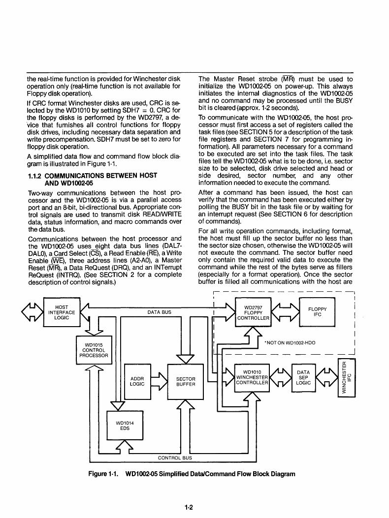
the real-time function is provided for Winchester disk operation only (real-time function is not available for Floppy disk operation).
If CRC format Winchester disks are used, CRC is selected by the WD1010 by setting SDH7 = O. CRC for the floppy disks is performed by the WD2797, a de-vice that furnishes ail control functions for floppy disk drives, including necessary data separation and write precompensation. SDH7 must be set to zero for floppy disk operation.
A simplified data flow and command flow block diagram is illustrated in Figure 1-1.
1.1.2 COMMUNICATIONS BETWEEN HOST AND WD1002·05
Two-way communications between the host processor and the WD1002-05 is via a parallel access port and an 8-bit, bi-directional bus. Appropriate control signals are used to transmit disk READIWRITE data, status information, and macro commands over the data bus.
Communications between the host processor and the WD1002-05 uses~ight data bus lines (DAL7-DALO), a Card Select (CS), a Read Enable (RE), a Write Enable (WE), three address lines (A2-AO), a Master Reset (MR), a Data ReQuest (DRQ), and an INTerrupt ReQuest (INTRQ). (See SECTION 2 for a complete description of control signals.)
HOST INTERFACE
LOGIC
WD1015 CONTROL
PROCESSOR
ADDR LOGIC
WD1014 EDS
DATA BUS
SECTOR BUFFER
CONTROL BUS
The Master Reset strobe (MR) must be used to initialize the WD1002-05 on power-up. This always initiates the internal diagnostics of the WD1002-05 and no command may be processed until the BUSY bit is cleared (approx. 1-2 seconds).
To communicate with the WD1002-05, the host processor must first access a set of registers called the task files (see SECTION 5 for a description of the task file registers and SECTION 7 for programming information). All parameters necessary for a command to be executed are set into the task files. The task files tell the WD1002-05 what is to be done, i.e. sector size to be selected, disk drive selected and head or side desired, sector number, and any other information needed to execute the command.
After a command has been issued, the host can verify that the command has been executed either by polling the BUSY bit in the task file or by waiting for an interrupt request (See SECTION 6 for description of commands).
For all write operation commands, including format, the host must fill up the sector buffer no less than the sector size chosen, otherwise the WD1002-05 will not execute the command. The sector buffer need only contain the required valid data to execute the command while the rest of the bytes serve as fillers (especially for a format operation). Once the sector buffer is filled all communications with the host are
I - - - - - - - - - - - - - -I
WD2797 FLOPPY
CONTROLLER
FLOPPY IFC
·NOT ON WD1002-HDO
WD1010 WINCHESTER CONTROLLER
DATA SEP
LOGIC
r
I I I I I
_-.J
Figure 1·1. WD1002·05 Simplified Data/Command Flow Block Diagram
1·2

terminated.
Multiple transfer commands are handled one sector at a time. If the host wants to transfer ten sectors, the \AJD1002-05 sequentially accepts one sector of data at a time and processes it until all sectors have been transferred. At the completion of the multiple transfer, the interrupt request is set, and the BUSY bit is cleared.
The data request (DRa) will always be set at the start of a write command, indicating that the sector buffer is available for sequentially inputting data. If the data request is set on a read command, it indicates that data requested by the host is in the sector buffer.
The interruot reauest (INTRa) is set after comoletion of a command. Status'and error information may now be read by the host.
1.2 SPECIFICATIONS
1.2.1 PERFORMANCE
DRIVE PARAMETERS
Encoding method: Cylinders: Sectors per track: Heads: Drive selects:
Step rate:
Data transfer rate: Write Precomp time: Sectoring:
WINCHESTER DISKS
MFM Up to 1024 Up to 64 8 3 (ST506)
3511s to 7.5 ms (500 I1sec increments)
5.0 Mbits/s 12 ns Soft
General X16 + X12 + X5 + 1
FLOPPY DISKS
MFM Up to 256 Upt064 2 4 (SA450)
rv1511S, 1 ms, 2ms, 3ms, 4ms, 5ms, 6ms, 8ms, 10ms, 12ms, 14ms, 16ms, 18ms, 20ms, 25ms, 40ms.
250 KbitS/s 100 to 300 ns adj. Soft
CRC polynomial: ECC polynomial: ECC polynomial reciprocal:
X32 + X28 + X26 + X19 + X17 + X10 + X6 + X2 + 1 X32 + X30 + X26 + X22 + X15 + X13 + X6 + X4 + 1
Non-detection probabi I ity: Miscorrection probability: Correction span: Single burst detection span: Double burst detection span:
Host interface: Drive capabi I ity: Drive cable length: Host cable length: Power requirements:
MTBF: MTTR:
1.2.2 PHYSICAL
Length: Width: Height:
1.2.3 ENVIRONMENTAL
256 byte sector
rv2.30 E-10 8.00 E-6 5 bits 20 bits 4 bits
8-bit bi-directional bus 10 LS loads 10 ft max 3 ft max + 5V ± 5% ,3.0 A max
10,000 POH 30 min.
8.00 in. 5.75 in. 0.75 in.
Ambient temperature ................... 0-50°C Relative Humidity (non-condensing) .... 20% - 800/0 Air flow at 1/4" from component surfaces .. 150 cubic ftJmin
1·3
512 byte sector
rv2.30 E-10 1.57 E-5 5 bits 19 bits 3 bits
SECTION 2
INTERFACE CONNECTORS
2.1 ORGANIZATION The WD1002-05 board has seven connectors for user application:
(J6) Power connector
(J5) Host interface connector
(J7, J8) Drive control connectors
(J1, J2, J3) Winchester high speed data connectors
The drive control cables are daisy-chained to each of the three Winchester drives. The three drive data connectors carry differential signals and are radially connected.
2.2 HOST INTERFACE CONNECTOR SIGNALS The signals of the host interface connector (J5) are compatible with most microprocessors and many minicomputers. The connector consists of an 8-bit bidirectional bus, a 3-bit address bus, and seven control lines. All commands, status, and data are transferred over this bus. The control signals are as follows:
DALO-DAL7 8-bit bi-directional Data Access Lines. These lines are in a high-impedance state whenever the CS line is inactive.
A2-AO
INTRQ
DRQ
When Card Select (CS) is active along with RE or WE, data is read or written via the DAL bus.
When Write Enable (WE) is active along with CS, the host may write data to a selected register of the WD1002-05.
When Read Enable (RE) is active along with CS, the host may read data from a selected register of the WD1002-05.
Three Address lines are used to select one of eight registers of the WD1002-05. They must remain stable during all read and write operations.
The INTerrupt ReQuest line is activated whenever a command has been completed. It is reset to the inactive state when the status register is read, or a new command is issued to the WD1002-05, or when MR is asserted.
The Data ReQuest line is activated whenever the sector buffer contains data to be read by the host, or is awaiting data to be loaded by the
2·1
MR
GND
host. This line is reset whenever the sector buffer is exhausted, or when MR is asserted.
The Master Reset (MR) line initializes all internal logic on the WD1002-05. Vvhenever ivi R is received by the WD1002-05, the internal diagnostics are automatically initiated.
All eVen numbered pins on this connector are to be used as signal grounds. Power grounds are available on the power connector.
2.3 4O·PIN HOST INTERFACE CONNECTOR The host interface connector (J5) is a 40-pin vertical header. Cabling should be less than three feet long. Either flat ribbon or twisted pair cable can be used. The connector pinouts are given in Table 2-1.
Table 2·1. Host Interface Connector Pin Description
Signal Signal Ground Pin Signal Name
2 1 DALO 4 3 DAL1 6 5 DAL2 8 7 DAL3
10 9 DAL4 12 11 DAL5 14 13 lJAL6 16 15 DAL7 18 17 AO 20 19 A1 22 21 A2 24 23 CS 26 25 WE 28 27 RE 30 29 Pull-up (PUP) 32 31 Not Connected 34 33 Not Connected 36 35 INTRQ 38 37 DRQ 40 39 MR
2.4 WINCHESTER DRIVE CONTROL SIGNALS The Winchester Drive Control connector (J7) is a relatively low-speed bus, daisy-chained to each of the Winchester drives in the system. To properly terminate the open collector outputs from the WD1002-05, the last drive in the daisy chain should have a 2201 330-0hm line termination resistor pack installed. All other drives should have no termination. Drive con-
trol signals are as follows:
RWG When the Reduce Write Current (RWC) line is activated with write gate, a lower write current is used to compensate for greater bit-packing density on the inner cylinders. The RWC line is activated when the cylinder number is greater than or equal to four times the contents of the write precomp register. This output is valid only during write and format commands.
WG The Write Gate signal enables the disk write data circuitry.
SC Seek Complete line informs the WD1oo2-05 that the head of the selected drive has reached the desired cylinder and has stabilized. Since Seek Complete is not checked after a seek command, overlapped seeks are allowed.
TROOO TRack 000 indicates that the R/W heads are positioned on the outermost cylinder. This line is sampled before each step pulse is issued.
WF Write Fault informs the WD1002-05 that some fault has occurred on the selected drive. The WD1oo2-05 will not execute commands when this signal is true.
HS2-HSO Head Select lines (HS2-HSO) are used by the WD1002-05 to select a specific R/W head on the selected Winchesterdrive.
IND Index is used to indicate the index pOint for synchronization during formatting and as a timeout mechanism for retries. This Signal should pulse once every rotation of the disc.
ROY Ready informs the WD1oo2-05 that the desired drive is selected and that its motor is up to speed. The WD1oo2-05 will not execute commands unless this line is true.
STE>P Step is pulsed once for every cylinder to be stepped. The direction of the step will be determined by the direction tine. The Step pulse period is determined by the internal Winct}e~ter,stepping rate register during .implied seek operations, or explicitly during seek commands. During auto
2·2
DS1-DS3
restore, the step pulse period is determined by the seek complete time from the drive.
These three Drive Select lines (DS1-DS3) are used to select one of three possible drives.
Direction In determines the direction of motion of the R/W head when the step line is pulsed. A high on this line defines the direction as out, and a low defines direction as in.
2.5 5.25" WINCHESTER 34-PIN DRIVE CONTROL CONNECTOR
This drive control connector (J7) is a 34-pin vertical header on 0.10-inch centers. Cabling should be flat ribbon or twisted-pair cable less than 10 feet long. The cable pinouts are given in Table 2.2.
Table 2-2. Winchester Drive Control Connector Pin Description
Signal Signal Ground Pin 1/0 Signal Name
1 2 0 RWC 3 4 0 Head Select 2 5 6 0 Write Gate 7 8 I Seek Complete 9 10 I TROOO
11 12 I Write Fault 13 14 0 Head Select 0 15 16 NC 17 18 0 Head Select 1 19 20 I Index 21 22 I Ready 23 24 0 Step 25 26 0 Drive Select 1 27 28 0 Drive Select 2 29 30 0 Drive Select 3 31 32 NC 33 34 0 Direction In
2.6 WINCHESTER DRIVE DATA CONNECTOR
Three data connectors (J1-J3) allow data to pass between the WD1002-05 and each Winchester disk drive. All lines associated with the transfer of data between a drive and the WD1002-05 system are differential in nature and may not be multiplexed. The three Winchester drive data connectors are 20-pin vertical headers on 0.10-inch centers. Cabling should be either flat ribbon or twisted-pair cable, less than 10 feet long. Cable pinouts are given in Table 2-3.

Table 2·3. Winchester Drive Data Connector Pin Description
I Sianal I Sianal I I Ground I Pin I I/O Signal Name
I 2 1 NC 4 3 NC I
6 5 ,NC 8 7 NC
9 NC I' 10 NC
11 GND 12 GND
13 0 M FM Write Data 14 0 MFM Write Data
15 GND 16 GND
17 I M FM READ Data 18 I MFM READ Data
19 GND 20 GND
2.7 POWER CONNECTOR
A 4·pin amp connector (J6) is provided for power and ground inputs to the board. The pinouts are given in Table 2-4.
Table 2-4. Power Connector Pin Description
Pin Signal Name
1 NC 2 GROUND 3 GROUND 4 + 5V regulated @ 3 amps (max)
2.8 FLOPPY DRIVE SIGNALS
The Floppy Drive Control connector (J8) is a relatively low-speed bus, daisy-chained to each of the floppy drives in the system. To properly terminate each TTLlevel output signal from the WD1oo2-05, the last drive in the daisy chain should have line terminations as specified by the drive manufacturer. The other drives should not have any terminations. Drive control signals for the floppy -diSCS are functionally similar to those for the hard discs, except that all data is transferred via one connector instead of the separate connectors used for the Winchester drives. Floppy drive signals are as follows:
I
The Index line contains a reference index pulse once every disk rotation to indicate the beginning of a track.
DS3-DSO
2·3
These four Drive Select lines (DS3-DSO) are used to select one of four possible drives.
The MOtOi On line is used to directly control the dc spindle motor of the floppy drive. !f Motor On Mode (MOM) = 0 (user selectable jumper option) then a 40 nsec delay occurs, otherwise a one-second delay occurs after Motor On and before any reading or writing is attempted. If the floppy drive is not accessed for "'3 seconds, the motor is turned off by the WD1015. Also the drives supported must be configured so that the R/W heads are loaded when the motor is turned on. This is usually available as an option on most drives.
The Direction In line determines the direction of motion of the R/W head when the step line is pulsed. A high on this line defines the direction as out, and a low defines the direction as in.
The Step line is pulsed once for each cylinder to be stepped. The direction of the step will be determined by the direction line. The step pulse period is determined by the internal floppy stepping rate register during implied seek operations, auto restore, or explicitly during seek and restore commands. During any restore operation, the stepping-rate period is limited to 8 ms minimum.
The Write Data interface line provides data to be written on the disk. This line is enabled by write gate being active.
The Write Gate output signal enables disk write data circuitry.
TROoo indicates that the R/W heads are positioned on the outermost cyl· inder. This line is sampled before each step is issued.
The Write Protect interface signal provided by the drive indicates to the WD1oo2-05 that a write-protected disk is installed. When write protect is active, no data can be written to the disk by the WD1002-05.

The Read Data line provides the "raw data" (clock and data together) as detected by the drive logic.
Selects side of floppy disk to be written or read.
2.9 5.25" FLOPPY 34-PIN DRIVE CONTROL CONNECTOR
This floppy drive control connector (J8) is a 34-pin vertical header on 0.10-inch centers. Cabling should be flat ribbon or twisted-pair cable, less than 10 feet long. The cable pinouts are given in Table 2-5.
2·4
Table 2·5. Floppy Drive Control Connector Pin Description
Signal Signal Ground Pin I/O Signal Name
1 2 - NC 3 4 - NC 5 6 0 Drive Select 0 7 8 I Index 9 10 0 Drive Select 1
11 12 0 Drive Select 2 13 14 0 Drive Select 3 15 16 0 Motor On 17 18 0 Direction In 19 20 0 Step 21 22 0 Write Data 23 24 0 Write Gate 25 26 I Track 000 27 28 I Write Protect 29 30 I Read Data 31 32 0 Side Select 33 34 - NC
SECTION 3
INTERFACE TIMING
3.1 HOST INTERFACE TIMING
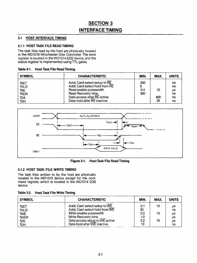
3.1.1 HOST TASK FILE READ TIMING
The task fiies read by the host are physicaiiy iocated in the WD1010 Winchester Disk Controller. The error register is located in the V'v'D1014 EDS device, and the status register is implemented using TTL gates.
Table 3·1. Host Task File Read Timing
SYMBOL
tSET tHLD tRE tRDR tDA tDH
ADDR
CHARACTERISTIC
Addr, Card select setup to RE Addr, Card select hold from RE Read enable pulsewidth Read Recovery til'lliL Data access after RE active Data hold after RE inactive
I
~tSET tHLD ---.:
~: I I I I I
X· ... 4:~~~~_tR_E_-_-_-_-_-_ --...... ::zr" I I I -.J ~tDH
MIN.
200 0 0.4 300
~tDA~r-_____ I
-------------« DATA VALID 7>-----DBO-7
Figure 3·1. Host Task File Read Timing
3.1.2 HOST TASK FILE WRITE TIMING
The task files written to by the host are physically located in the WD1 01 0 device except for the command register, which is located in the WD1014 EDS device.
Table 3·2. Host Task File Write Timing
I SYMBOL
I tSET tHLD twE twER tDS tDH
CHARACTERISTIC
Addr, Card select setup to WE Addr, Card select hold from WE Write enable pulsewidth Write Recovery time __ Data access se..!!:!2.. to WE active Data hold after WE inactive
3-1
MIN.
0.1 30 0.2 1.0 0.2 10
MAX. UNITS
ns ns
10 I-ls ns
400 ns 25 ns
MAX. UNITS
! 10 I I-ls
ns 10 I-ls
I-ls 10 I-ls
ns
AD DR ~ __________ A_0_,A_1_,A_2_ST_A_B_LE __________ ~ ____ __
tHLD~ ..--
CS ~ ...... __ tS_E_T--'_----&...: ________ --+-: _Jt+=---tW-E-R----.._~" __
I WE ------------" I I
~~--tWE---... 1t1
!.-- tDS ~:4- tDH I i~/~~~~
DATA MUST BE VALIDA><><>< DBO-7
Figure 3-2. Host Task File Write Timing
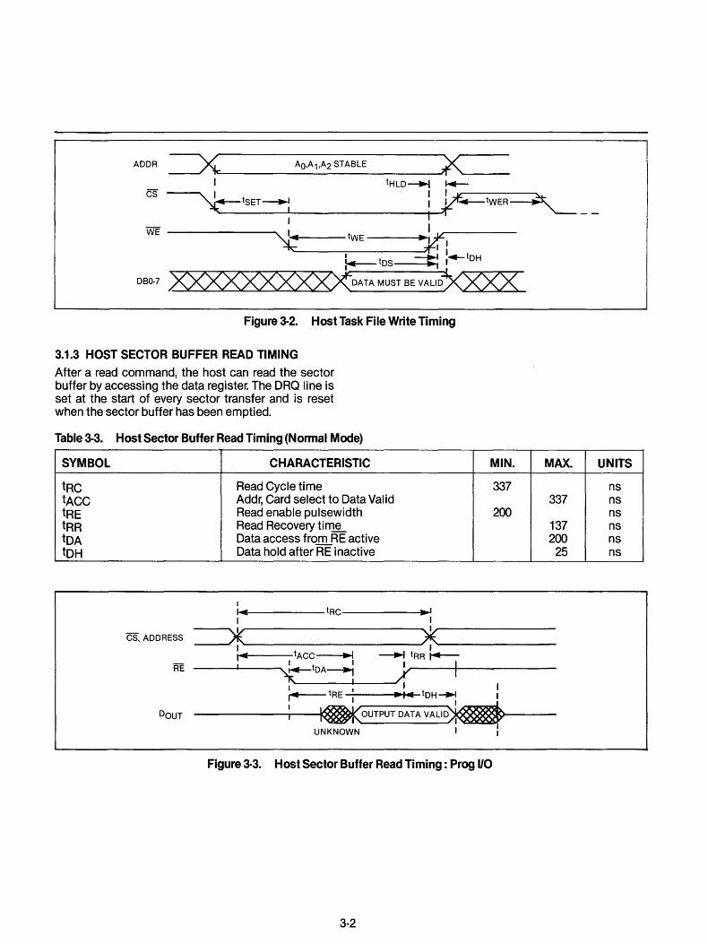
3.1.3 HOST SECTOR BUFFER READ TIMING
After a read command, the host can read the sector buffer by accessing the data register. The ORO line is set at the start of every sector transfer and is reset when the sector buffer has been emptied.
Table 3-3. Host Sector Buffer Read Timing (Normal Mode)
SYMBOL CHARACTERISTIC
tRC Read Cycle time tACC Addr, Card select to Data Valid tRE Read enable pulsewidth tRR Read Recovery tim~ tOA Data access from RE active tOH Data hold after RE inactive
I
1 ....... l------tRC .' I I
MIN.
337
200
MAX.
337
137 200
25
-~--~i ~--------------CS, ADDRESS ..-.-/!\ 7'\..
I I ,4 tACC -I ~ tRR 14--RE I &tDA~11 i I
~ . 1 , 14 tRE; -I'" tDH~ i
--------.----IOK OUTPUT DATA VALiD~"""""----UNKNOWN I I
DOUT
Figure 3·3. Host Sector Buffer Read Timing: Prog 1/0
3·2
UNITS
ns ns ns ns ns ns
ADDR,CS
I .... ; .. 1----tRC---II .. ~!111 1_----~.- ___ _=~~L============_+·===--=-=-~~~/======~ ~~: !.~ ~"=========
:.-tACC---+j : ... tRR .... 1 I I I --., tDA I.-! ..! 1 I
~~---....... --~ I Y-- -" y-====f~~-~--~--~---~= I I I t '"-----' 14= tRE I -rl DH ~
I 1 I
DOUT -----~ ~---~~--~~
Figure 3·4. Host Sector Buffer Read Timing: DMA Mode
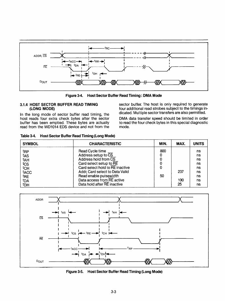
3.1.4 HOST SECTOR BUFFER READ TIMING sector buffer. The host is only required to generate four additional read strobes subject to the timings in· dicated. Multiple sector transfers are also permitted.
(LONG MODE)
In the long mode of sector buffer read timing, the host reads four extra check bytes after the sector buffer has been emptied. These bytes are actually read from the WD1014 EDS device and not from the
DMA data transfer speed should be limited in order to read the four check bytes in this special diagnostic mode.
Table 3·4. Host Sector Buffer Read Timing (Long Mode)
SYMBOL CHARACTERISTIC MIN. MAX. UNITS
tRP Read Cycle time _ 800 ns tAS Address setup to C~ 0 ns tAH Address hold from CS 0 ns tcs Card select setup to RE 0 ns tCH Card select hold to RE inactive 0 ns tACC Addr, Card select to Data Valid 237 ns tRE Read enable pulsewidth 50 ns tDA Data access from RE active 100 ns tDH Data hold after RE inactive 25 ns
ADDR =1 X\ x==-I ~ ~ tAS --..J tAH !~-I I I I
CS I
~ 1 l \ I I I
I I I I I
I I I 1 , I ~ tcs ~ tRF--" tCH~ !
1 1
.. - I I
RE ~ ! \ ,f I I I I
I'" tACC~ I ... TRP .' I
:.... ~I tDHt....--I
~ tDA I I
~ I
~ DOUT ~ ~ Figure 3·5. Host Sector Buffer Read Timing (Long Mode)
3·3

3.1.5 HOST SECTOR BUFFER WRITE TIMING
After a write or a format command has been issued, the host can write to the sector buffer by accessi ng the data register. Both the address lines A2-AO, and the CS line can be held in their active states without being toggled while writing the sector of data. The
DRO line is set at the start of every data transfer and is reset when the SB has been filled.
The DMA write cycle timing diagram is similar to the DMA read cycle timing shown in Figure 3-4.
Table 3·5. Host Sector Buffer Write Timing (Normal Mode)
SYMBOL CHARACTERISTIC MIN. MAX.
twc Write Cycle time 257 tAS Address setup time 0 tcw Addr, Card select to end of WE 257 twE Write enable pulsewidth 120 twR Write Recovery ti~ 137 tDS Data access from WE active 60 tDH Data hold after WE inactive 15
~I.~---------twc--------------~.~I
------*~-----------------------*---------1 I
ADDRESS
RE 1/!!111/& I \\\\\\\\\\\\~ 1 ..... I ... i-----tcw----~~~I I
cs ~\\\\\~~ lVillLb//J///I!/IA ~tAS" I 1 _____ tWE ----.I tWR I....---, ~ --i.~1 1
: \\\\ \\\\ \\ f , 1
l4-----tDS~:tDH ~ -----------------~ '1------------X DATA IN STABLE I -------------------~ I~----------
Figure 3·6. Host Sector Buffer Write Timing (Normal Mode)
3.1.6 HOST SECTOR BUFFER WRITE TIMING (LONG MODE)
In the long mode of sector buffer write timing, four extra check bytes are written by the host after the sector buffer has been fi lied. The bytes are actually written to the WD1014 EDS device and not to the sector buffer. The host is required to generate four additional write strobes subject to the timings indicated. Muftjpte sector transfers are permttted.
DMA data transfer speed should be limited in order to write the four check bytes in this special diagnostic mode.
3-4
UNITS
ns ns ns ns ns ns ns
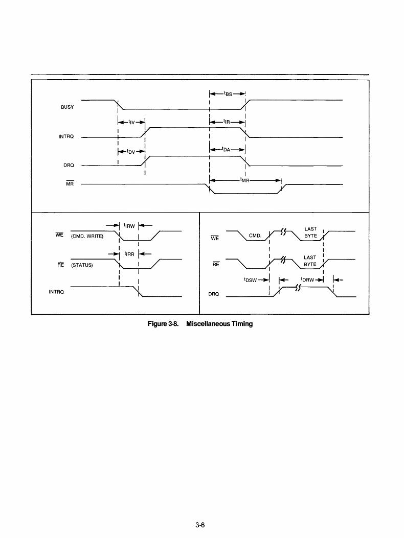
j.-tBS~
~ I X BUSY I
I.-tIV-+j
I I \.--tIR~
INTRa I Y : '} I I I I ~toA~1 J.-tOVj
I 1 I 1 ORO I I I
I - I .. tMR -I MR
~ /
~ tlRW t+-~~LASTI
WE (CMO. WRITE) ~ I / WE CMO. BYTE /' I
I I I I I I ~ tlRR ~ ~~ RE (STATUS) ~ I / RE BYTE
I I I I I
I tosw~ /4- tORW-+/ j.....-I
INTRa 'k DRO l,r-J~
Figure 3-8. Miscellaneous Timing
3-6

SECTION 4
HOST INTERFACING
4.1 GENERAL The WD1002-05 easily interfaces with most microcomputers and many minicomputers. Interfacing is accomplished with the host interface connector (J5).
The interface is very similar to that used for other 'fJestem Digital LS! peripheral devices, and the signal pinouts are compatible with the Western Digital WD1000 and WD1001 series of Winchester Disk Controller boards.
The WAIT line is not used in the WD1002-05. The WAIT signal, however, is still provided for compatibility with WD1000 and WD1001 controllers.
RESOUT READ
WR RD
A15
8085
4.2 HOST INTERFACING EXAMPLE Figure 4-1 shows the absolute minimum hardware required to interface the WD1002-05 board to a small 8085 microcomouter system. In the illustration. buffers are not used, nor -is the I/O completely decoded. The user will most likely want to completely decode the I/O to minimize the amount of I/O or memory space required in the host forWD1002-05 interfacing. If the interface cable length is kept to a few inches, it is often possible to directly interface the WD1002-05 to the buffered bus of a host microcomputer.
MR WAIT WE RE CS DAL7 DAL6 DAL5 DAL4 DAL3
74LS373 DAL2 WD1002
DAL1 DALO
ALE G AD7 8D 80 INTRO AD6 7D 70 DRO AD5 6D 60 AD4 5D 50 AD3 4D 40 AD2 3D 30 A2 AD1 2D 20 A1 ADO 10 10 AO
OC +5GND -V
AO·7
Figure 4-1. Host Interfacing Example
4-1

Table 3·6. Host Sector Buffer Write Timing (Long Mode)
I SYMBOL CHARACTERISTIC MIN. MAX. UNITS
I twp Write Cycle time _ 800 ns
tAS Address setup to C§...... 0 ns tAH Address hold from CS 0 ns tcs Card select setup to WE 0 ns tCH Card select hold to WE inactive 0 ns twE Write enable Rulsewidth 50 ns tos Data setup to WE inactive 60 ns tOH Data hold after WE inactive 15 ns
ADDR ~ __________________ ~¥~ ________________ ~x~ __ __ I I
I --.J tAS ~ ~ tAH l....-
I I ------'l~ I,------..\~ __ -----J/
Figure 3·7. Host Sector Buffer Write Timing (Long Mode)
3.2 MISCELLANEOUS TIMING
Table 3·7. Miscellaneous Timing
SYMBOL
I tlV tov
I tMR
I IBS tlR
I tDR
, tlRW tlRR tosw tORW
I I
I
CHARACTERISTIC
I NTRQ valid from BUSY inactive ORQ valid from BUSY inactive Master Reset pulsewidth M R to BUSY set MR to Interrupt reset MR to Data request reset WR (cmd.) to Interrupt reset RE (status) to Interrupt reset Write command to ORQ set WEIRE to DRQ reset
3-5
MIN.
50 I I
I
I I I
I
MAX.
60 60
200 200 200 200 200 200 300
!
I
UNITS
ns ns ms ns ns ns ns ns ns ns

SECTION 5
TASK FILE
S.1 TASK FILE BASICS
The WD1002-05 performs all disk functions through a set of registers called the task files. The task files are loaded with parameters such as sector numbei, cylinder number, etc., prior to issuing a command.
Table 5-1. Task File Register Array
CS A2 A1 AO
1 X X X 0 0 0 0 0 0 I 0 1 0 0 1 0 0 0 1 1 0 1 0 0 0 1 0 1 0 1 1 0 0 1 1 1
* Not used on floppies
Individual registers are selected via AO-A2 for both types of drives. The registers shown in Table 5-1 are ____ :1_1-1_
i:1Vi:1IIi:1UIt:::.
RE WE
Deselected Deselected Data Register Data Register Error Register Write Precomp* Sector Count Sector Cou nt Sector Number Sector Number Cylinder Low Cylinder Low Cylinder High* * Cylinder High** Size/Drive/Head Size/Drive/Head Status Register Command Register
* * LSB of cylinder high, if set to 1, permits a 48 t.p.L floppy disk to be read on a 96 t.p.L floppy disk system.
S.2 DATA REGISTER
This register is the user's window to the on-board full sector buffer. It contains the next byte of data to be written to or read from the internal sector buffer. When the ORO (Data Request) line is asserted, the sector buffer contains data to be read during a Type II command, or is awaiting data to be written during a Type III command. If the WD1002-05 is interfaced using programmed I/O, data transfers to this register can be implemented using programmed block moves. This register may not be read from or written to except in the context of a valid command.
S.3 WD1002·0S ERROR REGISTER
This Register contains specific fault information pertaining to the last command executed. This register is only valid if the error bit in the status register is set. The error register is read only. Table 5-2 shows the error register bits.
Table 5-2. Error Register Bits
Bit
7 6 5 4 3 2 1 o
Error Register
Bad Block Detect Uncorrectable Error CRC Error ID Field ID Not Found
Aborted Command TROOO Error DAM not found
S·1
DAM NOT FOUND Will be set during a read sector command if, after successfully identifying the 10 field, the data add ress mark was not detected within 16 bytes of ID field.
TROOO ERROR Will be set during a restore command if the track 000 line was not asserted by the drive after all stepping pulses have been issued. The Winchesters are issued a maximum of 1023 stepping pulses and the floppies, a maximum of 256 stepping pulses.
ABORTED Indicates that a valid command COMMAND has been received that cannot
be executed based on status information from the drive, Le. drive not ready, seek complete not asserted, or write fault. Interrogation of the status register by the host may be performed to determine the cause of this failure.
ID NOT FOUND When set, this bit indicates that an ID field containing a specified cyl i nder, head, sector number, or sector size was not found after all the retries have been executed.
UNCORRECTABLE Indicates that an ECC or CRC ERROR error was encountered in a data
field during a read sector command and the error was uncorrectable.
BAD BLOCK Indicates that a bad block mark DETECT has been detected in the speci
fied 10 field. If the command issued was a write sector command, write gate may be pulsed but the sector wi II not be written if generated from a read sector command, the data field will not be read. Note that bad block may not be detected if there is a flaw in the ID field.
5.4 DIAGNOSTIC ERRORS
On power-up, or when specifically commanded to, the WD1002-05 will run a series of internal diagnostic tests. When an error is encountered, the diagnostic routine is terminated. A binary error code is set in the error register without the error bit of the status register being set. The diagnostic routines are exercised in the following order:
Error Code
5 4 3 2 1
°
Major Functional Failure
WD1 015 error WD1014 or bus error sector buffer error WD1 01 ° error WD2797 error Pass - WD1002-05 is functional
5.5 WRITE PRECOMP
The write precompensation register holds the cylinder number where the RWC line will be asserted and write precompensation logic is to be turned on. This write-only register is loaded with the cylinder number divided-by-4 to achieve a range of 1024 cylinders. For example, if write precompensation is desired for cylinder 128 (80 Hex) and higher, this register must be loaded with 32 (20 Hex). The write precompensation delay is fixed. at 12 nanoseconds from nominal.
This register is not used for floppy disk drives. Floppy disk write precompensation is contained in WD2797 and set as described in the "Summary of Adjustment Procedure" in SECTION 9 (MAINTENANCE) of this manual.
5.6 SECTOR COUNT
The sector count register is used in read sector, write sector, and format commands to implement multiple
5·2
sector handling with one command. The value of zero implies a transfer of 256 sectors (any size). For read and write multiple sector commands, the sector count is decremented, and the sector number is incremented after each sector transfer to or from the buffer. During a format command, this register is loaded with the number of sectors to be formatted and decremented as each sector is formatted until it reaches zero. During format, sector numbers are specified using interleave tables loaded in the sector buffer.
5.7 SECTOR NUMBER
This register is loaded with the desired sector number prior to a read or write command. The sector number register may be read or written to by the host.
5.8 CYLINDER NUMBER
These two registers form the cylinder number where the head is to be positioned on a seek, read, or write command. The two least significant bits of the cylinder high register form the most significant bits of the cylinder number as illustrated below:
Cylinder High Cylinder Low
Re~isterb!ts: 171615141312111° 171615141312111°1 Cylmder bits: 9 8 7 6 5 4 3 2 1 °
When bit ° of the cylinder high register (bit 8 of cylinder registe" is set to a 1 during floppy operation, 48 tpi disks can be used in 96 tpi disk drives for all commands. When this bit is set to 0, only 96 tpi disks can be used.
5.9 SDH REGISTER
This register contains the ECC/CRC sector size, drive select, and head select bits. The SOH register is a read/write register organized as shown in Tables 5-3 through 5-7.
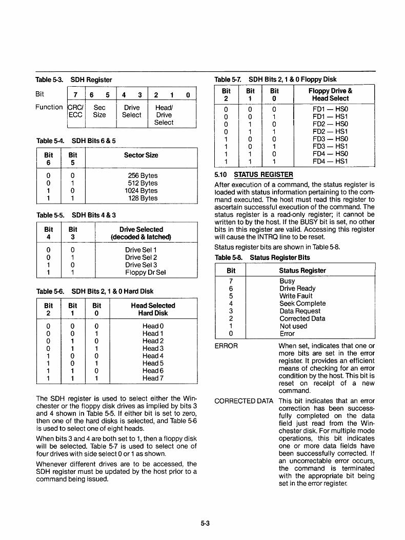
Table 5·3. SDH Register
Bit I 7 1
6 5 4 3 2 1 0
Function ~RC/I Sec Drive Head! ECC Size Select Drive
I I Select
Table 5·4. SDH Bits 6 & 5
Bit Bit Sector Size 6 5
I 0 0 256 Bytes 0 1 512 Bytes 1 0 1024 Bytes 1 1 128 Bytes
Table 5·5. SDH Bits 4 & 3
Bit Bit Drive Selected 4 3 (decoded & latched)
0 0 DriveSel1 0 1 DriveSel2 1 0 DriveSel3 1 1 Floppy Dr Sel
Table 5·6. SDH Bits 2, 1 & 0 Hard Disk
Bit Bit Bit Head Selected 2 1 0 Hard Disk
0 0 0 Head 0 0 0 1 Head 1 0 1 0 Head 2 0 1 1 Head 3 1 0 0 Head 4 1 0 1 Head 5 1 1 0 Head 6 1 1 1 Head 7
The SDH register is used to select either the Winchester or the floppy disk drives as implied by bits 3 and 4 shown in Table 5-5. If either bit is set to zero, then one of the hard disks is selected, and Table 5-6 is used to select one of eight heads.
When bits 3 and 4 are both set to 1, then a floppy disk will be selected. Table 5-7 is used to select one of four drives with side select 0 or 1 as shown.
Whenever different drives are to be accessed, the SDH register must be updated by the host prior to a command being issued.
5·3
Table 5·7. SDH Bits 2, 1 & 0 Floppy Disk
Bit
I Bit Bit Floppy Drive &
2 1 0 Head Select , 0 I 0 0 FD1- HSO 0 0 1 FD1 - HS1
I 0 1 0 FD2- HSO 0 1 1 FD2- HS1 I
I 1 0 0 FD3- HSO 1 0 1 FD3- HS1 1 1 0 FD4- HSO 1 1 1 FD4- HS1
5.10 STATUS REGISTER
After execution of a command, the status register is loaded with status information pertaining to the command executed. The host must read this register to ascertain successful execution of the command. The status register is a read-only register; it cannot be written to by the host. If the BUSY bit is set, no other bits in this register are valid. Accessing this register will cause the INTRQ line to be reset.
Status register bits are shown in Table 5-8.
Table 5-8. Status Register Bits
Bit Status Register
7 Busy 6 Drive Ready 5 Write Fault I 4 Seek Complete 3 Data Request 2 Corrected Data 1 Not used 0 Error
ERROR When set, indicates that one or more bits are set in the error register. It provides an efficient means of checki ng for an error condition by the host. This bit is reset on receipt of a new command.
CORRECTED DATA This bit indicates that an error correction has been successfully completed on the data field just read from the Winchester disk. For multiple mode operations, this bit indicates one or more data fields have been successfully corrected. If an uncorrectable error occurs, the command is terminated with the appropriate bit being set in the error register.

DATA REQUEST Functions the same as the DRQ line. When set, it indicates that the sector buffer is ready to accept data or contai ns data to be read by the host. The data request bit is reset when the sector buffer has been fully read or written. Normally, the host need not consult this bit to determine if a byte should be transferred.
SEEK COMPLETE Indicates the condition of the seek complete line on the selected Winchester drive. For Floppy drives, this line is asserted when the SDH register is reloaded.
WRITE FAULTI Indicates the condition of the WRITE PROTECT write fault line on a selected
Winchester drive. The WD1002-05 will not execute any command if this bit is set.
If a write-protected disk is sensed in a selected floppy drive during a write operation, the write fault bit will be set. The command will then be aborted and no writing will take place.
5-4
READY
BUSY
Indicates condition of ready line on drive. WD1002-05 will not execute any commands unless the ready bit is set. Normally this line is asserted for Floppy drives when the SDH register selects any floppy drive. A user available jumper option can be implemented if the READY line is available from the floppy drive.
After issuing a command, or initialing WD1002-05 internal diagnostics, this bit will be set indicating that the WD1002-05 is busy executing a command. No other bits or registers are valid when this bit is set.
5.11 COMMAND REGISTER All commands are loaded into this register after the task files have been set. Writing to this register will cause the INTRQ Line to be reset. The command register is a write-only register. Refer to SECTION 6 (COM MAN DS), subsection 6.1 for further details.
SECTION 6
COMMANDS
6.1 GENERAL
The WD1oo2-05 executes six, easy-to-use, macro commands. Most commands feature automatic "im-nlion" coo~ \Alhil"h rnO!lnc tho hnct c\l~torn noon nnt t-"''"'~ .... """"'." •• 1""" II."' ......... ..., ... ,"" •• ..., ...... """1""''''''''' •• .....,.....,"'" I.","
tell the WD1oo2-05 where the RlW heads of each drive are nor when to move them- The controller automatically performs all retries on errors encountered, including data ECC errors. If the RlW head mis-positions, the WD1002-05 will automatically perform a restore and a re-seek. If the error is completely unrecoverable, the WD1oo2-05 will simulate a normal completion to simplify the host's software.
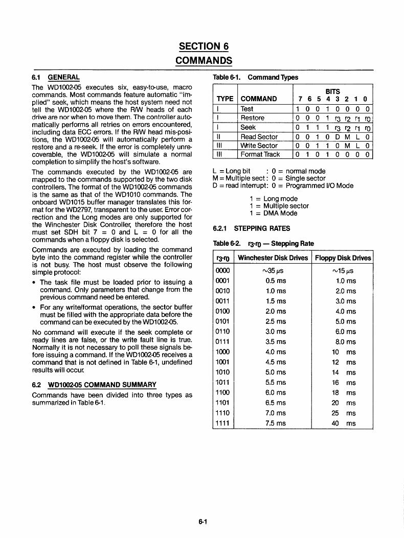
Table 6-1. Command Types
I TYPE I COMMAND I 7 6 5
II I Test 11 0 0 .. _ ....... - - - -
I Seek 0 1 1 II Read Sector 0 0 1 III Write Sector 0 0 1 III Format Track 0 1 0
L = Long bit : 0 = normal mode M = Multiple sect: 0 = Single sector
BITS I 43210
'v .t:,. • I 'V
1 r3 r2 r1 ro 0 D M L 0 1 0 M L 0 1 0 0 0 0
The commands executed by the WD1oo2-05 are mapped to the commands supported by the two disk controllers. The format of the WD1oo2-05 commands is the same as that of the WD1 01 0 commands. The onboard WD1015 buffer manager translates this format for the WD2797, transparent to the user. Error correction and the Long modes are only supported for the Winchester Disk Controller, therefore the host must set SDH bit 7 = 0 and L = 0 for all the commands when a floppy disk is selected.
D = read interrupt: 0 = Programmed I/O Mode
Commands are executed by loading the command byte into the command register while the controller is not busy. The host must observe the following simple protocol:
• The task file must be loaded prior to issuing a command. Only parameters that change from the previous command need be entered.
• For any write/format operations, the sector buffer must be filled with the appropriate data before the command can be executed by the WD1 002-05.
No command will execute if the seek complete or ready lines are false, or the write fault line is true. Normally it is not necessary to poll these signals before issuing a command. If the WD1oo2-05 receives a command that is not defined in Table 6-1, undefined results will occur.
6.2 WD1002-OS COMMAND SUMMARY
Commands have been divided into three types as summarized in Table 6-1_
6-1
1 = Long mode 1 = Multiple sector 1 = DMAMode
6.2.1 STEPPING RATES
Table 6-2. ra-ro - Stepping Rate
r3-ro Winchester Disk Drives
0000 ~35 I-is
0001 0.5 ms
1
0010 1.0 ms
0011 1.5 ms
0100 2.0 ms
0101 2.5 ms
0110 3.0 ms
0111 3.5 ms
1000 4.0 ms
1001 4.5 ms
1010 5.0 ms
1011 5.5 ms
1100 6.0 ms
1101 I 6.5 ms
I 1110 7.0 ms
11111 1 7.5 ms
Floppy Disk Drives
~15 I-is
1.0 ms
2.0ms
3.0 ms
4.0 ms
5.0ms
6.0 ms
8.0 ms
10 ms
12 ms
14 ms
16 ms
18 ms
20 ms
25 ms
40 ms
6.3 TYPE I COMMANDS
Type I commands do not effect transfer of data between the host and the WD1002-05 but merely position the RJW heads of the selected drive or run diagnostics. The restore and seek commands have explicit stepping rate fields. The lower four bits of these commands form the stepping rate for the drives.
6.3.1 TEST COMMAND
Bit code: 1 0 0 1 o· 0 0 0
The test command is used to run internal diagnostics for checking WD1002-05 board function. It is mainly employed to isolate faults in the board logic. This command is always executed on a MR strobe. Any faults are reported as error codes. (See Section 5.4 for a description of the error codes.)
6.3.2 RESTORE
Bit code: 0 0 0 1 R3 R2 R1 RO
The restore command is used to calibrate the position of the RJW head on each drive by stepping the head outward until the TROOO line goes true. Upon receipt of the restore command, the BUSY bit in the status register is set. Cylinder high and cylinder low registers are cleared. For Winchester operation, the actual stepping rate is determined by the Seek Complete period. For Floppy operation, a minimum stepping pulse of 8 msec. is used. However, the stepping rate field specified by the host is saved internally for use in all future implied seeks. The state of seek complete, ready and write fault are sampled, and if an error condition exists, the aborted command bit in the error register is set, the error bit in the status register is set, an interrupt is generated, and the BUSY bit is cleared.
Regardless of errors encountered, the internal head position register for the selected drive is cleared. The TROOO line is sampled. If TROOO is true, an interrupt is generated and the BUSY bit is reset. If TROOO is not true, stepping pulses at a rate determined by the stepping rate field are issued until the TROOO line is activated. When TROOO is activated, the busy bit is reset and interrupt is issued. If the TROOO line is not activated within 1024 stepping pulses, the TROOO error bit in the error register and the error bit in the status register are set, the BUSY bit is reset, and an interrupt is issued.
6·2
6.3.3 SEEK
Bit code: 0 1 1 1 R3 R2 R1 RO
The seek command positions the RJW head at a certain cylinder: It is primarily used to start two or more concurrent seeks on drives that support buffered stepping. Note that the seek complete line is not sampled after the seek command so that multiple seek operations may be started using drives with buffered seek capabi I ity.
6.4 TYPE II COMMANDS
Type II commands characteristically transfer blocks of data from the WD1002-05 buffer to the host. This type of command has an implicit stepping rate as set by the last restore or seek command.
6.4.1 READ SECTOR
Bit code: 0 0 1 0 D MOO
The read sector command is used to enable the host computer to read a sector of data from the disk. If ECC is enabled, ECC bytes are recomputed by the WD1002-05. After the buffer is full, the recorded ECC bytes are compared to the recomputed check bytes to generate the syndrome bytes. If the syndrome is non-zero, errors have occurred. Error correction is invoked by the WD1015 if two consecutive syndromes match, otherwise a maximum of 8 retries is attempted by the WD1015. If the data is correctable, the WD1015 makes the correction and passes the data in the buffer to the host. If, after eight retries, the syndromes do not match, the WD1002-05 sends an error status to the host along with the status from the WD1010. Multiple sector read commands are modified to single sector commands and are issued a multiple number of times. The status and error registers are updated for every block of data transferred.
During a Floppy read sector operation only CRC is used with the data fields. If a CRC error occurs in the data field, the WD1015 buffer manager attempts a maximum of 8 retries and reports the error only if it persists. Regardless of the drive accessed (Winchester or Floppy), CRC is used on alliD fields.
6.4.1.1 READLONG Command
Bit code: 0 0 1 0 D M 1 0
This command is similar to the read sector command except that the ECC operation producing the syndrome is inhibited in the WD1002-05. Instead, the W01002-05 copies the four recorded check bytes from the disk and passes them unaltered to the host. This command is useful in debugging and verifying the ECC hardware and software. To do this, first write

normally and then issue the REAOLONG command. The data, or the check bytes may now be altered by the host and written to the disk using the WRITELONG command. If a read command is now issued, the W01002-05 will correct it as long as the error induced is within the correction capability of the EGG polynomial. This mode is not supported for floppy disk.
6.4.1.2 DMA Read
o = OMA Read Mode
o = Programmed 110 mode 1 = OMAMode
The OMA bit is used to position INTRa in relation to OROs during the read sector command. If the OMA bit is reset (0 = 0), the interrupt will occur along with the ORO. This allows the programmed 1/0 host to intervene and transfer the data from the sector buffer. For programmed 1/0, multiple transfer is not permitted (M = 0). If the OMA bit is set (0 = 1), then the interrupt will occur only after the system OMA controller has transferred the entire buffer of data. This mode is always used with multiple sector transfers.
6.4.1.3 Normal Completion
A normal completion occurs when the W01002-05 encounters no errors. The BUSY bit is reset. The status of the OMA bit in the command byte is examined. If this bit is reset (0 = 0; programmed 1/0 mode), an interrupt is issued at this time. ORO is set until all bytes of data have been read from the buffer. (Note: It is recommended that programmed 1/0 transfers should take place as a block move without consulting the ORO bit in the Status Register.) After all the data has been moved from the buffer, the OMA bit in the command byte is consulted again. If this bit is set (0 = 1; OMA mode) then an interrupt will be issued.
6.5 TYPE III COMMANDS
This type of command is characterized by a transfer of a block of data from the host to the W01002-05 buffer. These commands have implicit stepping rates as set by the last restore or seek command.
The command wili not be executed by the W01002-05 controller unless the buffer has been completely filled by the host.
6·3
6.5.1 WRITE SECTOR
Bit code: 0 0 1 10M 0 0
The Write Sector command is used to write a sector of data from the host computer to the disk. Upon receipt of the write command, the controller sets ORO untii the entire sector iength of data has been written into the buffer. (Note: It is recommended that programmed 1/0 transfers should take place as a block move without consulting the ORO bit in the Status Register.)
6.5.1.1 WRITELONG Command
Bit code: 0 0 1 10M 1 0
The WRITELONG command functions similarly to the write sector command except that the EGG operation that computes the EGG word is inhibited in the W01002-05. Instead, the W01002-05 accepts a 4-byte appendage from the host and passes it unaltered to be written on the disc at the end of the data as check bytes. This mode is not supported for the floppy discs.
6.5.2 FORMAT TRACK
Bit code: 0 1 0 1 0 0 0 0
The format command is used for initializing the 10 and data fields on a particular disk. Upon receipt of the format command, the controller sets the ORO for the interleave table to be written to the buffer. In all cases, the number of bytes transferred to the buffer must correspond to the current sector size.
When the buffer has been completely filled, the specified number of sectors are written and the ORO is reset. The data field is written with 00 for the hard disks and E5 (hex) for the floppies. EGG or GRG bytes are automatically computed and written.
Once the index is found, a number of 10 and data fields are written to the disk. As each sector is written, the sector count register is decremented and consequently must be updated before each format operation.

SECTION 7
PROGRAMMING
7.1 GENERAL
Users will find programming the WD1oo2-05 relatively simple as a substantial amount of intelligence formerly required by host computers has been incorporated into the WD1 002-05 board.
The \'I./D1002-05 performs all needed retries, even on head positioning errors. If there is an error in the data field, the WD1oo2-05 will attempt to correct it.
Most commands feature automatic "implied" seek, which means that seek commands need not be issued to perform basic read/write functions. The WD1oo2-05 keeps track of the head position up to eight read/write head assemblies, eliminating the need for the host system to maintain track tables.
All transfers to and from disk are through an on-board sector buffer. This means that data transfers are fully interruptable and can take place at any speed that is convenient to the system designer. In the event of an unrecoverable error, the WD1oo2-02 simulates a normal completion so that special error recovery software is not needed.
This section assumes that the user has read Section 5 (Task File) and Section 6 (Commands).
7.2 SETTING UP TASK FILES
Before any of the six macro commands may be executed, a set of parameter registers called the task files must be set up. For most commands, this informs the WD1oo2-05 of the exact location on the disk where the data involved in the transfer is located or will be placed. For a normal read or write sector operation, the sector number, the size/drive/head, the cylinder number, and the command registers (usually in that order) wi II be written.
Note that although most of these registers are readable as well as writable, they are normally are not read from. Read capability for them is provided, however, so that error-reporting routines can determine physically where an error occurred without recalculating the sector, head, and cylinder parameters.
Since all the task file parameters can be recalled by the WD1oo2-05, it is recommended that task file parameters be stored in the WD1oo2-05 as they are calculated. This will save the programmer a few instructions and microseconds by not maintaining two copies of the same information.
7.2.1 CYLINDERS AND TRACKS
Since most hard-disk drives contain more than one head per positioner, it is more efficient to step the R/W head assemblies of most disk drives by cylinders, not tracks, In other words, the disk driver soft-
7=1
ware should be designed to read or write all data that is directly accessible by all the heads on a positioner before stepping to a new cylinder. Table 7-1 presents a cylinder-by-cylinder sequential file read on a four head, two-piatter disk drive.
Table 7·1. File Read on 4-Head, 2·Plaiter Disk Drive
Logical Physical Head Physical Physical Cylinder Number Head Side Platter
25 3 Top B 26 0 Bottom A 26 1 Top A 26 2 Bottom B 26 3 Top B 27 0 Bottom A
7.3 TYPE I COMMAND PROGRAMMING
Test, Restore and seek are Type I commands that position the R/W heads of the selected drive and set the implied stepping-rate register. No data is transferred to or from the data register. To execute a Type I command, the system software must perform the following functions in the order shown:
1. Set up task file and issue command with stepping rate (WD1oo2-05 will attempt to execute Type I command)
2. Wait for interrupt or for BUSY bit in status register to be reset
3. Check error bit in status register for proper completion
7.3.1 USE OF BUSY BIT
Smaller, single-user systems can sense the completion of a command by polling the BUSY bit of the status register. This bit (bit 7) is set whenever the controller starts a disk operation or internal diagnostics, and is reset whenever the controller is ready to communicate with the host computer.
On the WD1002-05, the BUSY bit is located in the same place as the sign bit of many computers to simplify the polling process.
One way to poll this bit using 8080 code is as follows:
WAIT: IN STATUS ;lnputWD1002-05 Status register
ANA A ;Update 8080 sign flag
J M WAIT ;Wait if BUSY (sign) bit set
I
I

This is another way to poll the BUSY bit using PDP-11 code:
WAIT: MOVB @#STATUS,R> ;Input status, update sign flag
BMI WAIT ;Wait if BUSY (N) bit set
7.3.2 USE OF INTERRUPTS
Another, more efficient way of notifying the CPU that the WD1oo2-05 has completed a command is through interrupts. The INTRQ line on the WD1oo2-05 makes a low to high transition whenever the disk controller requires CPU intervention. This allows the host CPU to run other tasks while the WD1oo2-05 is reading or writing data to the disk.
7.3.3 USE OF THE ERROR BIT
As the WD1oo2-05 simulates normal completions when errors have been encountered, the only way to determine error status is to check the error bit in the status register. The WD1002-05 error bit is so located that it can be easily tested by rotating it into the carry bit of many processors. The contents of the error register are not valid unless the error bit is set.
One way to check the Error bit using 8080 code is as follows:
IN STATUS
RAR
JC ERROR
;Get status (if not al ready inA) ; Rotate error bit intoC ;Jump if error found
In certain hardware configurations, the following can check the error bit using PDP-11 code:
BIT @#STATUS,#1 ;Bit test the error bit BNE ERROR ;Branch if error
found
7.3.4 USE OF THE CORRECTED BIT
Correctable errors are usually quite benign and can almost always be ignored. Some systems designers, however may wish to log their occurrence. The corrected bit has been placed in the status register to facilitate error logging. Correctable and fatal errors can be detected with the following 8080 code:
IN STATUS ;Get WD1oo2-05 status
ANI 5 ;Mask off Error and Correct bits
JNZ SOMERR ;Jump if we have either a ;correctable or fatal error
7·2
7.4 TYPE II COMMAND PROGRAMMING
The only Type II command is the read sector command. This command is characterized by the transfer of a block of data from the WD1oo2-05 buffer to the host. The command features implied seek with an implicit stepping rate. To execute a Type II singlesector command in programmed I/O mode, the system software must perform the following functions in the order shown:
1. Set up task file and issue command with DMA bit reset (WD1 002-05 will attempt to read sector)
2. Wait for interrupt or for BUSY bit in status register to be reset
3. Perform a block move from WD1oo2-05 buffer to system memory
4. Check error bit in status register for proper completion
Note: Steps 3 and 4 above can be reversed.
To execute a Type II single or multiple sector command in DMA mode with interrupts, the system software does the following:
1. Set up task file and issue command with DMA bit set
2. Set up DMA controller (WD1002-05 will attempt to read single or multiple sectors) (DMA controller will move data from WD1002-05 to memory)
3. Wait for interrupt from WD1002-05
4. Check error bit in status register for proper completion
Note: The above sequence is preferred, but steps 1 and 2 above can be reversed.
7.4.1 DMA MODE
The DMA mode bit (D) in the foregoing read sector examples is a special bit in the command byte used to optimize the WD1002-05 interrupts during programmed 1/0 and DMA operations. If the DMA bit is reset (D = 0), the interrupt will come before the buffer is transferred. This allows a programmed 1/0 host to intervene and transfer the buffer of data. If the DMA bit is set (D = 1), then the interrupt will occur only after the data has been transferred. This allows the host to go uninterrupted until the entire buffer has been transferred.
7.4.2 BLOCK MOVES
The WD1002-05 performs all transfers between itself and the disk drive through an on-board full sector buffer. Once the disk has been read, the data is available to the host at any rate from DC to as high as a byte

every 500 ns. In programmed 1/0 applications there is no need to consult the DRO bit in the status register to determine if another byte is ready to be processed. Once an interrupt occurs or the BUSY bit is reset on a read, the host computer should do a block move of all the bytes in the sector.
The following 8080 code demonstrates a transfer from the WD1oo2-05 to system memory. The transfer address is in HL and the byte count is in B:
READ IT: I N DATA ;Get data from WD1oo2-05 sector buffer
MOV M,A ;Store it in memory INX H ;Increment memory
pOinter DCR B ;Decrement byte
counter JNZ READIT ;Do it again if whole
sector not xferred
The following Z-80 instruction does it all. The transfer address is in HL, byte count is in Band WD1002-05 data register address in C:
READIT: INIR ;Transfer buffer from WD1oo2-05 to memory
7.4.3 USING DMA
A special bit in the read sector command optimizes the WD1oo2-05 in terrupts for DMA operation.
7.4.4 MULTIPLE SECTOR TRANSFERS
The WD1oo2-05 can transfer more than one sector per command, if interfaced, using DMA and interrupts. Transfers as large as an entire track can be executed. The sector count register holds the number of records to be transferred (if sector count is zero, then 256 records will be transferred.) The sector number register holds the starting sector of the transfer. When a multiple sector transfer is successfully completed, the sector count register will be equal to zero and the sector number register will be equal to the last sector transferred plus one.
If a fatal error is encountered during a multiple sector transfer, the sector number register will be left pointing to the sector that contained the fatal error, and the sector count register will hold the number of sectors that were not transferred.
tf a correctabfe error is encountered during a multiple sector read, the corrected bit in the status register will be set, but the operation will not be terminated because correctable errors are not considered fatal.
7-3
7.4.4.1 Partial Sector Transfers
The WD1oo2-05 permits partial sector transfers on read operations. This allows the user to read the first part of a sector and discard the rest. During programmed 1/0, the byte counter in the block move routine is set to the number of bytes to be read. During DMA operations, the DMA controller is set with the number of bytes to be transferred.
Normally, during a DMA read operation, the WD1002-05 interrupts the host after a sector has been transferred. However, if only a partial sector is being read, the WD1oo2-05 does not know that the operation has been completed. Therefore, the 'transfer complete' interrupt must come from the DMA controller.
During write sector operations, the DMA controller will interrupt the system after the buffer has been transferred to the WD1oo2-05, but before the data have been written. Some systems with advanced interrupt handling capabilities can easily mask off this spurious DMA interrupt. For those systems that cannot, the WD1oo2-05 has a provision built into its command structure to detect read operations.
7.4.4.2 Interrupt Source Selection
Bit 4 of all commands determines whether the operation will be a read sector operation or something else. Those commands that require the interrupt from the WD1oo2-05 have this bit set to 1. The read sector command (the only one that might need the DMA controller's interrupt) has this bit set to a O. Bit 3 of the command is then used to select either programmed 1/0 interrupts or DMA type interrupts.
7.4.4.3 Clearing Hardware DRQ
During partial sector reads, the DMA controller will stop the DMA transfer before the WD1oo2-05 has a chance to issue its last data request. Because of this, the DRO line might be set the next time transfer parameters are sent to the DMA controller. To avoid spurious (and often fatal) DROs, the user must do a hardware clear of the DRO line unless another command is issued. DRO is actually cleared by doing dummy reads of the data register to dump the rest of the data.
7.4.4.4 Interrupt Selection Circuit
If the user is reading partial sectors with the WD1oo2-05 and wants to have the system automaticaUy configure its interrupts! a circuit similar to that shown by Figure 7-1 will have to be implemented.
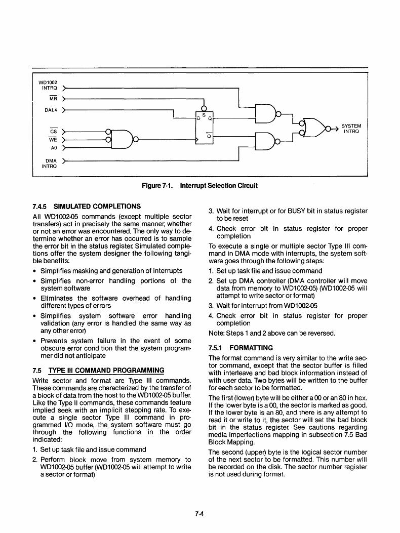
WD1002 INTRQ
~ MR I
DAL4 ) r.4:, u u
SYSTEM CS INTRQ
WE Q
AO
DMA INTRQ
Figure 7·1. Interrupt Selection Circuit
7.4.5 SIMULATED COMPLETIONS
All W01002-05 commands (except multiple sector transfers) act in precisely the same manner, whether or not an error was encountered. The only way to determine whether an error has occurred is to sample the error bit in the status register. Simulated completions offer the system designer the following tangi· ble benefits:
• Simplifies masking and generation of interrupts
• Simplifies non·error handling portions of the system software
• Eliminates the software overhead of handling different types of errors
• Simplifies system software error handling validation (any error is handled the same way as any other errory
• Prevents system failure in the event of some obscure error condition that the system program· mer did not antiCipate
7.5 TYPE III COMMAND PROGRAMMING
Write sector and format are Type III commands. These commands are characterized by the transfer of a block of data from the host to the W01 002-05 buffer. Like the Type II commands, these commands feature implied seek with an implicit stepping rate. To execute a Single sector Type III command in programmed I/O mode, the system software must go through the following functions in the order indicated:
1. Set up task file and issue command
2. Perform block move from system memory to W01002·05 buffer (W01002·05 will attempt to write a sector or format)
7·4
3. Wait for interrupt or for BUSY bit in status register to be reset
4. Check error bit in status register for proper completion
To execute a single or multiple sector Type III command in OMA mode with interrupts, the system software goes through the following steps:
1. Set up task file and issue command
2. Set up OMA controller (OM A controller will move data from memory to WD1002-05) (W01002-05 will attempt to write sector or format)
3. Wait for interrupt from W01002-05
4. Check error bit in status register for proper completion
Note: Steps 1 and 2 above can be reversed.
7.5.1 FORMATTING
The format command is very similar to the write sector command, except that the sector buffer is filled with interleave and bad block information instead of with user data. Two bytes will be written to the buffer for each sector to be formatted.
The first (lowery byte will be either a 00 or an 80 in hex. If the lower byte is a 00, the sector is marked as good. If the lower byte is an 80, and there is any attempt to read it or write to it, the sector will set the bad block bit in the status register. See cautions regarding media imperfections mapping in subsection 7.5 Bad Block Mapping.
The second (uppery byte is the logical sector number of the next sector to be formatted. This number will be recorded on the disk. The sector number register is not used during format.
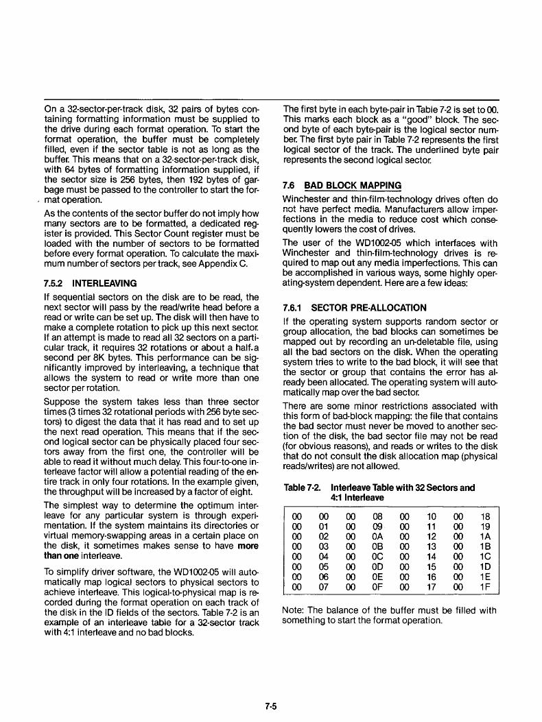
On a 32-sector-per-track disk, 32 pairs of bytes containing formatting information must be supplied to the drive during each format operation. To start the format operation, the buffer must be completely filled, even if the sector table is not as long as the buffer. This means that on a 32-sector-per-track disk, with 64 bytes of formatting information supplied, if the sector size is 256 bytes, then 192 bytes of garbage must be passed to the controller to start the for-
. mat operation.
As the contents of the sector buffer do not imply how many sectors are to be formatted, a dedicated register is provided. This Sector Count register must be loaded with the number of sectors to be formatted before every format operation. To calculate the maximum number of sectors per track, see Appendix C.
7_5.2 INTERLEAVING
If sequential sectors on the disk are to be read, the next sector will pass by the read/write head before a read or write can be set up. The disk will then have to make a complete rotation to pick up this next sector. If an attempt is made to read all 32 sectors on a.particular track, it requires 32 rotations or about a half-.a second per 8K bytes. This performance can be significantly improved by interleaving, a technique that allows the system to read or write more than one sector per rotation.
Suppose the system takes less than three sector times (3 times 32 rotational periods with 256 byte sectors) to digest the data that it has read and to set up the next read operation. This means that if the second logical sector can be physically placed four sectors away from the fi rst one, the controller wi II be able to read it without much delay. This four-to-one interleave factor will allow a potential reading of the entire track in only four rotations. In the example given, the throughput will be increased by a factor of eight.
The simplest way to determine the optimum interleave for any particular system is through experimentation. If the system maintains its directories or virtual memory-swapping areas in a certain place on the disk, it sometimes makes sense to have more than one interleave.
To simplify driver software, the W01002-05 will automatically map logical sectors to physical sectors to achieve interleave. This logical-to-physical map is recorded during the format operation on each track of the disk in the 10 fields of the sectors. Table 7-2 is an example of an interleave table for a 32-sector track with 4:1 interleave and no bad blocks.
7·5
The first byte in each byte-pair in Table 7-2 is set to 00. This marks each block as a "good" block. The second byte of each byte-pair is the logical sector number. The first byte pair in Table 7-2 represents the first logical sector of the track. The underlined byte pair represents the second logical sector.
7.6 BAD BLOCK MAPPING
Winchester and thin-film-technology drives often do not have perfect media Manufacturers allow imperfections in the media to reduce cost which consequently lowers the cost of drives.
The user of the W01002-05 which interfaces with Winchester and thin-film-technology drives is required to map out any media imperfections. This can be accomplished in various ways, some highly operating-system dependent. Here are a few ideas:
7.6.1 SECTOR PRE·ALLOCATION
If the operating system supports random sector or group allocation, the bad blocks can sometimes be mapped out by recording an un-deletable file, using all the bad sectors on the disk. When the operating system tries to write to the bad block, it wi II see that the sector or group that contains the error has already been allocated. The operating system will automatically map over the bad sector.
There are some minor restrictions associated with this form of bad-block mapping: the file that contains the bad sector must never be moved to another section of the disk, the bad sector file may not be read (for obvious reasons), and reads or writes to the disk that do not consult the disk allocation map (physical reads/writes) are not allowed.
Table 7·2. Interleave Table with 32 Sectors and 4:1 Interleave
00 00 00 08 00 10 00 00 01 00 09 00 11 00 00 02 00 OA 00 12 00 00 03 00 OB 00 13 00 00 04 00 OC 00 14 00 00 05 00 00 00 15 00 00 06 00 OE 00 16 00 00 07 00 OF 00 17 00
18 19 1A 1B 1C 10 1E 1F
Note: The balance of the buffer must be filled with something to start the format operation.
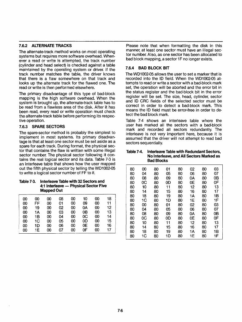
7.6.2 ALTERNATE TRACKS
The alternate-track method works on most operating systems but requires more software overhead. Whenever a read or write is attempted, the track number (cylinder and head select) is checked against a table maintained by the operating system or driver. If the track number matches the table, the driver knows that there is a flaw somewhere on that track and looks up the alternate track for the flawed one. The read or write is then performed elsewhere.
The primary disadvantage of this type of bad-block mapping is the high software overhead. When the system is brought up, the alternate-track table has to be read from a flawless area of the disk. After it has been read, every read or write operation must check the alternate-track table before performing its respective operation.
7.6.3 SPARE SECTORS
The spare-sector method is probably the simplest to implement in most systems. Its primary disadvantage is that at least one sector must be set aside as a spare for each track. During format, the physical sector that contains the flaw is written with some illegal sector number. The physical sector following it contains the real logical sector and its data. Table 7-3 is an interleave table that shows how the user mapped out the fifth physical sector by telling the WD1oo2-05 to write a logical sector number of FF to it.
Table 7·3. Interleave Table with 32 Sectors and
00 00 00 FF 00 19 00 1A 00 1B 00 1C 00 1D 00 1E
4:1 Interleave - Physical Sector Five Mapped Out
00 08 00 10 00 00 01 00 09 00 00 02 00 OA 00 00 03 00 OB 00 00 04 00 OC 00 00 05 00 OD 00 00 06 00 OE 00 00 07 00 OF 00
18 11 12 13 14 15 16 17
7·6
Please note that when formatting the disk in this manner, at least one sector must have an illegal sector number. Also, as one sector has been allocated to bad block mapping, a sector 1 F no longer exists.
7.6.4 BAD BLOCK BIT
The WD1oo2-05 allows the user to set a marker that is recorded into the ID field. When the WD1oo2-05 attempts to read or write a sector with a bad-block mark set, the operation will be aborted and the error bit in the status register and the bad-block bit in the error register will be set. The size, head, cylinder, sector and 10 CRC fields of the selected sector must be correct in order to detect a bad-block mark. This means the ID field must be error-free in order to detect the bad block mark.
Table 7-4 shows an interleave table where the user has marked all the sectors with a bad-block mark and recorded all sectors redundantly. The interleave is not very important here, because it is assumed that the driver will not attempt to read bad sectors sequentially.
Table 7·4. Interleave Table with Redundant Sectors, No Interleave, and All Sectors Marked as Bad Blocks
80 00 80 01 80 02 80 03 80 04 80 05 80 06 80 07 80 08 80 09 80 OA 80 OB 80 OC 80 OD 80 OE 80 OF 80 10 80 11 80 12 80 13 80 14 80 15 80 16 80 17 80 18 80 19 80 1A 80 1B 80 1C 80 1D 80 1E 80 1F 80 00 80 01 80 02 80 03 80 04 80 05 80 06 80 07 80 08 80 09 80 OA 80 OB 80 OC 80 OD 80 OE 80 OF 80 10 80 11 80 12 80 13 80 14 80 15 80 16 80 17 80 18 80 19 80 1A 80 1B 80 1C 80 1D 80 1E 80 1F
SECTION 8
THEORY OF OPERATION
8.1 GENERAL
The WD1002-05 Winchester Floppy Disc Controller (WFC) is a stand-alone general purpose controller board designed to provide a buffer interface between a host controller and a combination of up to three Winchester disc drives and four floppy disk drives. The WD1002-05 is fabricated using a proprietary chip set designed specifically for Winchester Floppy disc control.
The design of the WD1002-05 circuitry implements all of the logic required for host interface, WD1002-05 internal diagnostics, variable length sector buffer, task files, ECC diagnostics and correction, data separation, and WD1002-05 control. The Winchester drive signals from the host controller are based upon the floppy look-alike interface with the Seagate Technology ST506 and other compatible drives. All necessary drive signal decoding for the floppy disc drives is performed solely by the WD1002-05 so that the host controller sees only Winchester drive signal format.
8.2 WD1002·05 ARCHITECTURE AND FUNCTIONAL DESCRIPTION
The internal structure of the WD1002-05, illustrated in Figure 8·1, consists of six major functional blocks as well as all necessary support logic. They are as follows:
1. Host Interface Logic (HIL)
2. Buffer Manager Control Processor (CP)
3. Error Detection and Support Logic (EDS)
4. Sector Buffer (SB)
5. Winchester Disc Drive and Buffer Interface (WDBI)
6. Floppy Disc Drive and Buffer Interface (FDBI)
The host can communicate with the Winchester or floppy disc via the SB. On power·up, the host is required to strobe MR which in turn causes the WD1002-05 to execute a speCial TEST command that initiates internal diagnostic routines within the WD1002-05 to ensure the functionality of the WD1002-05. The internal diagnostic routines can also be exercised by the host explicitly, in addition to five other macro commands used to execute disk operations. The six macro commands are as follows:
1. TEST
2. RESTORE
3. SEEK
4. READ
5. WRITE
6. FORMAT
8·1
Prior to issuing any command to the WD1002-05, the host must first set up command parameters in the task file registers, i.e. sector size, drive select information, settor number accessed, etc. The host must then fill the sector buffer with the required data if either a WRITE or FORMAT command is to be executed by the WD1002-05. The WD1002-05 BUSY status bit is set when the sector buffer has been filled by the host, or immediately upon receipt of any other type of command from the host. The WD1002-05 then executes the command issued, at which time all communications between the host and the WD1002-05 are suspended. The only access available to the host is the ability to poll the status of the BUSY bit. The command issued by the host is read by the CP from the command register in the task file, interpreted, and re-issued to either the Winchester or floppy disk processor, or executed directly by the CPo Upon completion of the command, the WD1002-05 sets the INTRa/DRa lines, dependant upon the type of command issued, and clears the BUSY bit. At this time, the host can read status and error information from the task files before issuing another command.
8.2.1 HOST INTERFACE LOGIC (HIL)
The HIL contains the requisite logic to buffer all datal command access between the host, the WD1002-05, the WD1010, and the WD2797 controllers. Bus protocol is exactly the same as the WD1010 Hard Disc Controller device. All data and command information is transferred on an 8-bit DAL bus. This tristate asynchronous bus is controlled by the host, only if the WD1002-05 is not BUSY. The host accesses the WD1002-05 ~resenting a stable address (AO-A2) along with a RE or WE strobe qualified bY' CS. The direction of transfer is determined by the RE and WE signals. For DMA transfers, the WD1002-05 provides a DRa signal to inform the DMA controller of a pending transfer. HIL also produced INTRa for interrupts after commands, or to signal a transfer completion for Interrupt Driven Systems. The host may reset the WD1002-05 by asserting MR (if MR is asserted, the WD1002-05 internal diagnostics routine is initiated and the host must wait for BUSY to be cleared before issuing a command to the WD1002-05).
The HIL passes DATA and COMMANDS to the EDS and CP along with processed strobes derived from WE, RE, CS, and A2-AO signals. HIL receives DATA and STATUS from the EDS and CP along with control information concerning DRa and INTRa generation.

HOST 1/0 BUS
WD1015 CONTROL PROCESSOR (CP)
SECTOR BUFFER (SB)
1K X 8
WD1014 ERROR DETECTIONI SUPPORT LOGIC (EDS)
- MFMRD
+MFMRD DATA -MFMWD SEPARATORI WRITE +MFMWD PRECOMP, R[5r1-RO~ (:'j)
DS1-DS3 (3)
WG
SDH LATCH, RWC
WINCHESTER STEP PULSE WINCHESTER
WD1010 DRIVE BUFFER DIR IN DI~IVE 110
WINCHESTER INTERFACE (MAX3
DRIVE (WDBI) DmVES)
CONTROLLER (WDC) TNi)"E'5(
.. TROOO SEEK COMP
WRITE FLT
READY
,.. .,;--------- -------1 __ -/ .. READ DATA -
WD2797 FLOPPY DRIVE
Wm"77,;~~ CONTROLLER (FDC)
I
TKOO 4_-
FLOPPY DISC INDEX DRIVE BUFFER WRITE PROTECT INTERFACE (FDBI)
SIDE SELECT L ____ --,
17'.b777.~~'TTH777.~'7'777'TT'.Q.A,.,_,~~/h,.,..,..,.,..". 0 I I I
STEP
FLOPPY DISC DIRIVE 1/0 (MAX 4 DI=!IVES)
20 MHZ Cl CLOCK GENERATOR
1 MHZ
2 MHZ
5 MHZ
10 MHZ
f f DATA BUS
~ CONTROL BUS I I I I I I
MOTOR ON
DSO-DS3 4
LNOTONWD1002-HDO ___ _ _ _ ._. __ --1
Figure 8·1. WD1002·0SIWD1002·HDO Functional Block Diagram

8.2.2 CONTROL PROCESSOR (CP)
The main control center of the WD1002-05 is the CP (WD1015), used in conjunction with the EDS (WD1014) device, the clock generator, and the task files (TSF). The EDS device is the right hand of the CP and of sufficient complexity to be treated as a separate functional entity.
The CP controls the transfer of information within the WD1002-05 and maintains the necessary copies of the TSF found on both drives. Host access to the WD1002-05 causes the CP to access task file information in the TSF after a command is issued. The TSF are physically located in the controller chips and on-board external logic is used to reflect any changes such as error and status information required to integrate the floppy format to that of the Winchester controller. Depending upon the command, the CP will make the buffer accessible to the host, the WD1 01 0, or the WD2797 controllers.
The CP also controls the operation of the Error Correcting logic. During the transfer of data from the host to the WD1010, the EDS monitors the data bus (if so enabled), to compute a 4-byte ECC which is a~ pended to the end of the data transferred to the WD1010 and recorded on the disc. During data transfers from the WD1 01 0 to the host, the CP uses the ECC to validate the data. If the data is corrupted, the CP envokes recovery techniques such as retries and correction. A maximum of eight retries are attempted if two consecutive syndromes do not match. Correction is attempted only if two consecutive syndromes match. If the error is uncorrectable, the operation is terminated.
The CP is also used to handle data transfers to and from the SF for the floppy disc controller, which only uses CRC check byte for its data fields.
During status reads by the host, the CP consolidates the normal completion status from the WD1010, the WD2797, and the current EDS status into a form consistant with established WD1010 error reporting format. This consolidated status is then presented to the host.
8.2.2.1 Clock Generator
The 20 MHz oscillator drives the Clock Generator which provides all timing clocks for the WD1002-05.
The crystal frequency divided by 2 is used as a reference clock (2XDR) and then divided again by 2 for a 1X clock (WCLK) which is used to clock the WD1010.
The Floppy Disc Controller (WD2797) operates with a 1 MHz clock for 5.25" drives. 2XDR divided by 10 is used to produce the required 1 MHz clock.
8·3
!he C~ uses a 10 MHz clock (2XDR), giving an instruction cycle time of 1.5 I-ls. Most instructions execute i n 3~O I-ls, or two cycles.
8.2.2.2 Task/Syndrome File (!SF)
The TSF provides on-chip storage of the required task fi les for the WD1 01 0IWD2797 controllers and the 4 bytes of syndrome used for ECC. The cheCk! syndrome bytes are physically stored in the ECC generator/checker. The WD1014 (EDS) maintains its own ?ommand register which serves also as an error regIster upon command completion. All other registers compriSing the TSF are physically part of the WD1010 and WD2797 controllers. The CP controls all access to the TSF. Refer to separate sections on task files for their use.
8.2.3 ERROR DETECTION AND SUPPORT LOGIC (EDS)
The WD1014 EDS chip provides the WD1002-05 with Err?r Correction Capabilities (ECC) and support logic. The EDS chip is a single chip device specifically designed to add ECC to the 5.25" Winchester disc drives. The EDS also contains three 8-bit registers, three counters, and several latches that enhance the CP capabilities for control functions in a real time operation. This 40 pin chip replaces approximately 35 TTL packages consisting of shift registers, flip-flops, and combinatorial logic gates.
8.2.3.1 Error Detection
The EDS processes all data transfers in either direction between the S8 and the WD1 01 0, if SDH bit 7 is set. This bit should only be set for hard disc operation. The EDS generates the ECC/SYN DROM E bytes by using a polynomial division process which can provide unique code words for long streams of data. The polynomial selected is a computer generated code optimized for sector sizes of 128, 256, 512, and 1024 byte data fields. During NormallWrite operation this division process produces a 32-bit remainde~ which is used as the four ECC bytes. In Normal/Read operation, the ECC bytes are recomputed and compared to the recorded ECC bytes to generate the Four SYNDROME bytes. If the syndrome is zero, there were no errors detected. Otherwise, the nonzero syndrome is used by the CP to compute the displacement of the error vector within the bad sector. This information is then used to correct the data if a stngte burst of no more than 5 bits in error occurred.
During a WRITELONG operation, the EDS is inhibited from computing the 32 bit ECC word. The EDS then accepts a 32-bit appendage from the host and passes
it on, unaltered, to the WD1010 to be recorded on the disk. This permits the host to induce errors anywhere in the data stream so that the operation of the EDS can be validated during a subsequent READSHORT operation. Durina a READLONG ooeration. the EDS is inhibited frorn producing a syndrome. Instead, it copies the recorded ECC check bits and passes them unaltered to the host, appended to the end of the sector da~a being read. As with WRITELONG, this command IS
useful when validating EDS performance.
The EDS uses a 2-bit serial implementation of the generator polynomial during ECC generation and error detection. During correction operations, a serial reverse polynomial is used by the CP to compute the error vector and displacement. Correctable errors are corrected in the buffer without host intervention. Uncorrectable errors are reported to the host and the uncorrected data is transferred to the host for further action.
8.2.3.2 Support Logic
The support logic consists of two 8-bit latches (command/error register and SOH latch). Data requests, interrupts, BUSY, multiple mode, and read command information is also maintained and updated in the WD1014 to enhance the capability of the CP to handle control functions in real time.
The EDS controls the buffer counter, incrementing and presetting due to commands from the host, and contains all the necessary logic to handle sector buffer overflow. Data, buffer addresses, and Drive/Head select control are handled by the same multiplexed 8-bit address and data bus.
8.2.4 SECTOR BUFFER (SB)
The S8 is used to buffer a sector of data being transferred to or from the host. The sector size may be programmed for 128, 256, 512, or 1024 bytes. Thus, the minimum RAM size required is 1 KX8. The address counters are controlled by the CP and EDS. All control signals for SB access are provided by 'the WD1010, or the CP when communicating with the floppy controller rND2797).
8.2.5 WINCHESTER DRIVE AND BUFFER INTERFACE (WDBI)
The WDBI consists of the Winchester Disc Controller rND1010), an 8-bit SOH latch, write precomp logic rNPC), data separator, and appropriate drivers and receivers. The WD1010 is connected to the Winchester drives and the SB by means of 20 signal lines that form the WDBI. As previously mentioned, the
8·4
WD1002-05 uses a multiplexed data/address bus to share SB access and control lines with the WD1010. Proper use of this interface results in having only a presettable counter to control the buffer and a latch/decoder to control up to three Winchester drives. The counter is preset using two separate strobes, one for each byte of the address, one 8-bit counter package provides addressing capability for a 128 or 256 byte sector buffer size. By using more than one counter package, the WD1002-05 permits a multiple sector buffer size of 64K bytes. The SOH latch is used to provide drive selects 1-3 and head selects 0-7.
8.2.5.1 Write Precompensation (WPC)
The generation of Modified Frequency Modulation (MFM) write data takes place in the WD1010. This device accepts a byte of data and a WCLK to produce MFM data through internal circuitry which decides when and where to write clocks and data on the data stream under the MFM encoding rules. The MFM data stream is now totally compatible with the recording rules and may be sent to suitable line drivers for transmission to the drive except for one modification. Due to the decreasing radius on the physical surface of the disk, the inside tracks have less circumference and therefore exhibit a increase in recording flux density over the outside tracks. This increase in flux density aggravates a problem in magnetic recording known as 'dynamic bit shift.'
Dynamic bit shift comes about as the result of one bit on the disk (a flux reversal) influencing an adjacent bit. The effect is to shift the leading edge of both bits closer together or further apart than recorded. The net result is that enough jitter is added to the data recorded on the inside tracks to make them harder to recover without error.
Write precompensation is used to reduce the effect of dynamic bit shift. It is a way of predicting which direction a particular bit will be shifted and intentionally writing that bit out of position in the opposite direction to the expected shift. This is done by examining the next two data bits, the last and the present bits to be written and producing three signals depending on what these bits are. The three signals are EARLY, LATE and NOMINAL. They are used in conjunction with a delay line to cause the leading edge of a data or clock bit to be written earlier, later, or on time.
The processor can enable or disable the generation of these signals by controlling the Write Pre-Comp rNPC) line from the addressable latch. When WPC is high, precomp is in effect. When WPC is low, no precomp is generated and the nominal output of the device is held true.

8.2.5.2 Data Separator
Data is recorded on Winchester discs using an MFM technique. This technique requires clock bits to be recorded only when two successive data bits are missing in the serial data stream. The fact that clock bits are not recorded with every data bit cell requires circuitry that can remain in sync with data during the absence of clock bits. Synchronous decoding of MFM data streams requires the decoder circuitry to synthesize clock bit timing when clock bits are missing and synchronize to clock bits when they are present. This is accomplished by using a phase-locked oscillator employing an error amplifier and filter to sync onto and hold a specific phase relationship to the data and clock bits in the data stream. The phaselock occurs at 2x average data rate frequency (fo), which in turn is used to synthesize a clock called RCLK with a frequency = 1/2 fo. This synthesized clock can then be used to separate data bits from clock bits with external logic to shift the resultant serial data into registers for byte parallelization within the WD1010.
8·5
8.2.6 FLOPPY DRIVE AND BUFFER INTERFACE (FDBI)
The FDBI consists of a Floppy Disc Controller tyVD2797), a drive select latch, head load, motor-on, buffer management logic, and appropriate drivers and receivers. The write precomp and data separator are internal to the WD2797. The WD1oo2-05 can support up to four 5.25" floppy drives, double density and single ordouble sided tyVD1002-05 only).

SECTION 9
MAINTENANCE
9.1 GENERAL
When the board is shipped from the factory, all adjustments have been made using ST506 and SA450 drives. The user need not make any adjustments if the drives supported are compatible with the forementioned drives.
There are four adjustments associated with the WD1002-05 on-board data separation/write precomp circuitry and VCO that might have to be made if a drive with a different data rate is installed. On the WD2797, the write precompensation value is adjustable and the data separator might have to be adjusted for drives of different data rates.
9.2 OSCILLATOR FREQUENCY
Data separation circuitry on the WD1002-05 uses a voltage-controlled oscillator (V co) which phase-locks onto incoming data and provides a clock suitable for separating data and clock bits on an MFM-encoded data stream. The V co must be adjusted using the following procedures:
Connect a frequency counter to Test Connector U30-10 (V co OUT).
Connect a DVM to Test Connector U30-1 (Vci IN).
Make all connections to the board, including the host and drive. Adjust the variable capacitor C19 until the frequency output locks onto the desired center frequency for the drive being used which is 10.000 MHz for ST506 or compatable drive. Once this "locked-on" frequency is achieved, continue the same adjustment for an input voltage of 2.5 ± 0.5 V.
To complete the adjustment, monitor RCLK and RDATA inputs to the WD1010 (U19-39,37 respectively) and fine tune variable capacitor C19 until the rising edge of RDATA is exactly centered in either Half Phase or RCLK.
1-- 200 NSEC NOM
RCLK ,4 t3 -I if I ~I
I I I
I RDATA I
I
I
j.-t1 ·1-- t2~ t1 = t2
t1 + t2 = t3
9·1
9.3 WD2797 ADJUSTMENT PROCEDURE
WRITE PRECOMPENSATION
Strobe M R (U 15-19).
Jumper across E3-E4.
Observe pulse width on WD (U15-31).
Adjust WPW (U15-33/R24) for desired pulse width (Precomp Nominal Value).
DATA SEPARATOR
Observe pulse width on TG43 (U15-29).
Adjust RPW (U15-18/R25) for 1/8 of the read clock (500 ns for 5.25" DD).
Observe frequency on DIRe (U15-16).
Adjust variable capacitor (C7) on Veo pin (U15-26) for Data Rate (250 KHz for 5.25" DD)
Remove jumper between E3-E4.
Note: To maintain interval Veo operation, insure that TEST = 1 whenever a Master Reset pulse (MR) is applied.
9.4 TEST/OPERATION JUMPER VARIATIONS
1. E1 to E2 N.A.
2. E16 to E15 N.A.
3. E4 to E3 Normally open. Ground for Floppy Write Precomp/Data Separator adj. only.
4. E8/E10 to E9 GND (E8-E9) = No Write Precomp. Open = Write Precomp always. E10 to E9 = Write Precomp aboveTG43.
5. E5/E7 to E6 E5 to E7 = Normal READY latch. E6 to E7 = If FRDY line available from Floppy drive.
6. E11 to E12 GND = 40msec MOM delay. OPEN = 1 sec MOM delay.
7. E13 to E14 N.A.
8. E17/E19 to E18 E18 to E19 = 10 MHz. E18 to E17 = 20 MHz.
9. E20 to E21 N .A.
10. E22 to E23 N.A.
11. E24 to E25 N.A.

APPENDIX A DISK DRIVER EXAMPLES
A.1 INTRODUCTION
The two sample disk drivers presented in this appendix are intended to serve as a catalyst to help the user set up his own first driver. Note that although the drivers shown are simplistic, they represent everything needed to satisfy WD1002-05 operating requirements. Retry software is not included in the examples because all necessary retries are performed by the WD1 002-05.
The first example shown is a programmed 1/0 and polled status driver using the 8-bit Intel 8085 microprocessor. The second example is of a programmed 1/0 and interrupt driven driver and is written for the 16-bit Western Digital WD16 microprocessor.
A.2 POLLED STATUS DRIVER
;***********************************************;
WD1002·05 Hard Disk Controller Driver Example for 8085 Microprocessor
with programmed 1/0 and polled status
;***********************************************;
;This driver is intended to demonstrate one simple approach to writing a ;driver for the WD1002-05. It assumes that the WD1002-05 is interfaced using ;programmed 1/0 without interrupts.
;The specifications of the imaginary demonstration drive are:
;Sector size: 256 bytes ;Sectors per track: 33 ;Surfaces per drive: 4 (two platters) ;Cylinders per drive: 512 ;Stepping rate: 2 milliseconds STRATE = 2 ;Define stepping rate for assembler
;As the WD1002 is being allowed to map around the bad blocks, one ;sector per track has to be sacrificed. This brings down the logical ;sector per track count to 32.
;Experienced systems programmers will note that the driver is not ;being made as flexible as it should be. As WD1002-05 compatible drives will ;be introduced in the future, and present manufacturers will be ;increasing the density of their current drives, the driver written ;should be built with sufficient equates and conditional ;assemblies.
;The imaginary operating system of this example can access up to 65536 ;Iogical records of 256 bytes each. It has three types of calls: ;initialize, read, and write. Three numerical parameters are passed ;in the following registers:
Drive number C Logical record number DE Transfer address H L
;Upon completion of all commands, the carry bit of the 8085 will be ;reset if the operation terminated properly and set if there was an ;error. If there was an error during read or write, the error-handling ;routine will decode it and print it out on the user console.
A-1

;************************; EaUATES
; * * * * * * * * * * * * * * * * * * * * * * * *;
; * * * Port Definition * * * BASADD = DATA = ERROR = WPC = SECNT = SECNO = CYLLO = CYLHI = SOH = STATUS = COMND =
oca BASADD BASADD+1 BASADD+1 BASADD+2 BASADD+3 BASADD+4 BASADD+5 BASADD+6 BASADD+ 7 BASADD+ 7
; * * * Command Definition * * * REST = 10 READ = 20 WRITE = 30
A.2.1 INITIALIZATION
; * * * * * * * * * * * * * * * * * * * * * * *; INITIALIZE
; * * * * * * * * * * * * * * * * * * * * * * *;
;Base address of WD1002-05 ;Data register ;Error Register ;Write Precomp ;Sector Cou nt ;Sector Number ;Cylinder Number ;Cylinder High ;Size/Head/Drive ;Status register ;Command register
;Restore command ;Read command (programmed 110 mode) ;Write command
;This routine is called once whenever the system is powered up or reset. ;It sets the stepping rate and restores the head on the selected drive.
RESTOR: CALL UPTASK ;Select drive, don't care about record MVI A,REST + <STRATE*2> ;Get stepping rate and restore OUT COMND ;Output command to WD1002-05
RSWAIT: IN STATUS ;Wait 'till restore done ANA A ;by updating sign flag in 8085 JM RSWAIT ;and wait 'till bit 7 (Busy) goes low RAR ;Put error bit in carry RET ;Return to operating system
A.2.2 READ SECTOR
; * * * * * * * * * * * * * * * * * * * * * * *; READ
; * * * * * * * * * * * * * * * * * * * * * * *;
;This is the read routine for the imaginary operating system.
READIT: CALL UPTASK ;Update WD1002-05 task file MVI A, READ ;Get READ command OUT COMND ;Output command to WD1002-05
;Wait for WD1 002-05 to read ina sector
RWAIT: IN STATUS ANA A JM RWAIT
;Check Busy bit ;by updating sign flag in 8085 ;and wait 'till bit 7 goes low
A·2
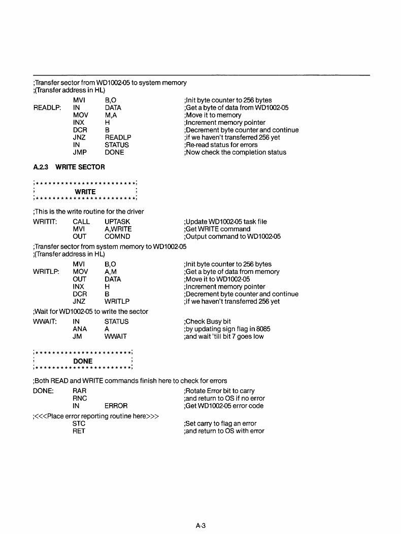
;Transfer sector from WD1oo2-05 to system memory ;(Transfer address in HL)
READLP: MVI IN MOV INX DCR JNZ IN JMP
B,O DATA M,A H B READLP STATUS DONE
A_2.3 WRITE SECTOR
; * * * * * * * * * * * * * * * * * * * * * * * *; WRITE
;************************;
;This is the write routine for the driver
WRITIT: CALL UPTASK MVI A,WRITE OUT COMND
;Init byte counter to 256 bytes ;Get a byte of data from WD1oo2-05 ;Move it to memory ;Increment memory pointer ;Decrement byte counter and continue ;if we haven't transferred 256 yet ;Re-read status for errors ;Now check the completion status
;Update WD1oo2-05 task file ;Get WRITE command ;Output command to WD1 002-05
;Transfer sector from system memory to WD1oo2-05 ;(Transfer address in HL)
MVI B,O WRITLP: MOV A,M
OUT DATA INX H DCR B JNZ WRITLP
;Wait for WD1 002-05 to write the sector
WWAIT: IN STATUS ANA A JM WWAIT
; * * * * * * * * * * * * * * * * * * * * * * *; DONE
; * * * * * * * * * * * * * * * * * * * * * * *;
;Init byte counter to 256 bytes ;Get a byte of data from memory ;Move it to WD1002-05 ;Increment memory pointer ;Decrement byte counter and continue ;if we haven't transferred 256 yet
;Check Busy bit ;by updating sign flag in 8085 ;and wait 'till bit 7 goes low
;Both READ and WRITE commands finish here to check for errors
DONE: RAR ;Rotate Error bit to carry RNC ;and return to OS if no error IN ERROR ;Get WD1oo2-05 error code
;«<Place error reporting routine here»> STC RET
;Set carry to flag an error ;and return to OS with error
A-3
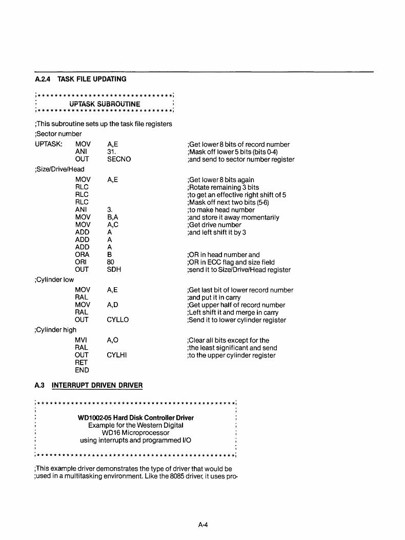
A.2.4 TASK FILE UPDATING
;********************************; UPiASK SUBROUiiNE
;********************************;
;This subroutine sets up the task file registers
;Sector number
UPTASK: MOV ANI OUT
;Size/Drive/Head
MOV RLC RLC RLC ANI MOV MOV ADD ADD ADD ORA ORI OUT
;Cylinder low
MOV RAL MOV RAL OUT
;Cylinder high
MVI RAL OUT RET END
A,E 31. SECNO
A,E
3. B,A A,C A A A B 80 SDH
A,E
A,D
CYLLO
A,O
CYLHI
A.3 INTERRUPT DRIVEN DRIVER
;Get lower 8 bits of record number ;Mask off lower 5 bits (bits 0-4) ;and send to sector number register
;Get lower 8 bits agai n ;Rotate remaining 3 bits ;to get an effective right shift of 5 ;Mask off next two bits (5-6) ;to make head number ;and store it away momentari Iy ;Get drive number ;and left shift it by 3
;OR in head number and ;OR in ECC flag and size field ;send it to Size/Drive/Head register
;Get last bit of lower record number ;and put it in carry ;Get upper half of record number ;Left shift it and merge in carry ;Send it to lower cylinder register
;Clear all bits except for the ;the least significant and send ;to the upper cylinder register
;***********************************************;
WD1002·05 Hard Disk Controller Driver Example for the Western Digital
WD16 Microprocessor using interrupts and programmed I/O
;***********************************************;
;This example driver demonstrates the type of driver that would be ;used in a multitasking environment. Like the 8085 driver, it uses pro-
A-4
;grammed 1/0 for data transfers. Unlike the last driver, this one ;supports interrupts.
;This new driver uses the same drive used in the 8085 example.
;Like the last driver, this one can access up to 65536 logical records ;of 256 bytes each. It still has three types of calls: initialize, read, ;and write. Three numerical parameters are passed in the following ;registers:
Drive number R1 Logical record number R2 Transfer address R3
;Upon completion of all commands, the carry bit of the WD16 will be ;reset if the operation terminated properly and set if there was an ;error. If there was an error during read or write, the error-handling ;routine will decode it and print it out on the user console.
; * * * * * * * * * * * * * * * * * * * * * * * *; EQUATES
; * * * * * * * * * * * * * * * * * * * * * * * *;
;* * * Port Definition *** BASADD = OFFD8 DATA = BASADD ERROR = BASADD+ 1 WPC = BASADD+1 SECNT = BASADD+2 SECNO = BASADD+3 CYLLO = BASADD+4 CYLHI = BASADD+5 SOH = BASADD+6 STATUS = BASADD+ 7 COMND = BASADD+ 7
;*** Command Definition *** REST = 10 READ = 20 WRITE = 30
; * * * Drive stepping rate * * * STRATE = 2
A.3.1 INITIALIZATION
; * * * * * * * * * * * * * * * * * * * * * * *; INITIALIZE
; * * * * * * * * * * * * * * * * * * * * * * *;
;Base address of WD1002-05 ;Data register ;Error Register ;Write Precomp ;Sector Count ;Sector Number ;Cylinder Number ;Cylinder High ;Size/HeadlDrive ;Status register ;Command register
; Restore command ;Read command (programmed 1/0 mode) ;Write command
;Drive stepping rate
;This routine is called once whenever the system is powered up or reset. ;It sets the stepping rate and restores the head on the selected drive.
RESTOR: CAll UPTASK ;Setect drive, don't care about record
;As a multitasking computer is being interfaced with, ;the calling job should be put to sleep while the restore is being done. ;The SLEEP instruction in this listing is actually a monitor call to
A-5
;the operating system which does the dirty work. Once the WD1002-05 has ;completed the restore, it will interrupt the CPU and the interrupt ;routine will wake the job. Putting the job to sleep will allow other ·t!lC!VC! tn IICO tho r.DII \Alhilo tho roctnro ic in nrnnrocc ,1.II.AV.'\....., .. "" U""""'" "'I'" "' • ...., •••••• ...., "'II....., • .....,...., ... ....,."" • ...., .,. ,..,.._~. ___ •
LOCK •• ,,' I IVIVV #REST + <STRATE*2>,@#COMND
;Disable interrupts until sleep ;Get stepping iate and i6StOi6
SLEEP MOVB RORB RTN
A.3.2 READ SECTOR
10WAIT @#STATUS,RO RO
; * * * * * * * * * * * * * * * * * * * * * * *; READ
; * * * * * * * * * * * * * * * * * * * * * * *;
;and output command to WD1 002-05 ;Put job in an 1/0 wait state ;Get status register ;Put error bit in carry ;Return to operating system
;This is the read routine for the imaginary operating system.
READIT: CALL UPTASK ;Update WD1002-05 task file LOCK ;Disable interrupts 'til we go to sleep MOVB #READ,@#COMND ;Issue READ command to WD1002-05
;Wait forWD1002-05 to read in a sector
SLEEP 10WAIT ;While waiting, go into 1/0 wait state
;After wakeup, transfer sector from WD1002-05 to system memory ;(Transfer address in R3, WD1002-05 data register address in R4)
MOV #256.,RO ;Init byte counter to 256 bytes
;The following instruction, MABB (Move Address to Block of Bytes), does ;a block move by reading the data pOinted to by R4 (WD1002-05 data ;register) and puts them in a block of memory pOinted to by R3. RO bytes ;are moved.
MABB BR
A.3.3 WRITE SECTOR
R4,R3 DONE
; * * * * * * * * * * * * * * * * * * * * * * * *; WRITE
; * * * * * * * * * * * * * * * * * * * * * * * *;
;This is the write routine for the imaginary driver
WRITIT: CALL UPTASK MOVB #WRITE,@#COMND
;Move data from WD1002-05 to memory ;Now check the completion status
;Update WD1002-05 task file ;Issue WRITE command to WD1002-05
;Transfer sector from system memory to WD1002-05 ;(Transfer address in R3, WD1002-05 data register address in R4)
MOV #256.-1.,RO ;Init byte counter to 256-1 bytes
;The following instruction, MBBA (Move Block of Bytes to Address) is the ;converse of the MABB instruction, above. This time the block of memory ;pointed to by R3 will be moved to the WD1002-05 data register (pointed to ;by R4). RO bytes will be moved.
A-6
MBBA R3,R4 LOCK MOVB @R3,@R4
;Wait for WD1 002-05 to write the sector
SLEEP 10WAIT
; * * * * * * * * * * * * * * * * * * * * * * *; DONE
; * * * * * * * * * * * * * * * * * * * * * * *;
;Move most of the data ;Disable ints. 'till last byte xferred ;Write last byte of data to WD1 002-05
;Wait in I/O wait state
;Both READ and WRITE commands finish here to check for errors
DONE: MOVB @#STATUS,RO ;Get status byte from WD1002-05 RORB RO ;Rotate Error bit to carry BCC DONEOK ;and return to OS if no error MOVB @#ERROR,RO ;Get WD1oo2-05 error code
;«<Place error reporting routine here»>
LCC CARRY DONEOK: RTN
A.3.4 TASK FILE UPDATING
;********************************; UPTASK SUBROUTINE
;********************************;
;This subroutine sets up the task file registers
;Sector number
UPTASK: MOV AND MOV MOVB
;Size/Drive/Head
R2,RO #31.,RO #SECNO,R4 RO,(R4)+
;Set carry to flag an error ;and return to OS with error
;Get record number ;Mask off lower 5 bits (bits 0·4) ;Index WD1002-05 sector number register ;and send to sector number register ;and increment R4 to pOint to WD1002-05 ;Cylinder Low register
;(The following instruction does a right arithmetic shift 5 times)
SSRA R2,5 ;Discard SECNO bits from record number MOV R2,RO ;Get remaining record number bits AND #3.,RO ;Mask off bits 5-6 to make head number
;(The following instruction does a left arithmetic shift 3 times)
SSLA R1,3 ;Shift drive number into position OR R1,RO ;OR drive number and head together OR #80,RO ;OR ECC flag and sector size field MOVB RO,@#SDH ;send it to Size/Drive/Head register
;Cylinder Low
SSRA MOVB
R2,2 R2,(R4) +
;Discard HEAD bits from record number ;Send Cylinder Low to WD1002-05 and ;increment R4 to point to Cylinder High
A-7

;Cylinder High ;(The following instruction SWAps the upper and lower Byte of a word)
SWAB R2 ;Get upper byte of cylinder AND #1,R2 ;Mask to ieast significant bit MOVB R2,(R4) ;and send it to WD1002-05 MOV #DATA,R4 ;index \lVOloo2-05 Data Reg for RlVI/ ops RTN
A.3.S INTERRUPT SERVICE ROUTINE
;***************************************; INTERRUPT SERVICE ROUTINE
;***************************************;
;This routine gets called whenever the WD1002-05 interrupts. All it does is ;read the status register of the WD1002-05 to clear INTRQ and revives the ;original calling job.
INTSER: PUSH RO MOVB @#STATUS,RO WAKEUP 10WAIT POP RO RTT END
;Save this register ;Acknowledge the interrupt to WD1002-05 ;Wake up job (from I/O wait state)
;Return from trap
A-8

APPENDIX B INTERLEAVE CALCULATING
This BASIC program simplifies the process of generating interleave tables. It is written in a fairly standard subset of the BASIC language and should run on many BASIC interpreters and compilers. Some implementations of BASIC may require the variable names to be converted to single letter names and the IF THEN ELSE constructs may have to be rewritten.
The two questions at the beginning of the program should be answered in decimal. The interleave table is printed in hexadecimal.
BASIC INTERLEAVE CALCULATING PROGRAM 10 PRINT "WD1oo2-05lnterleave calculating program" 20 PRINT 30 INPUT "Number of sectors? ";COUNT 40 INPUT "Interleave Factor? ";INTER 50 DIM HEX$(16),SECTOR(COUNl) 60 FOR INDEX = 1 TO 16 70 READ HEX$(INDEX) 80 NEXT 90 FOR INDEX = 1 TO COUNT
100 SECTOR(INDEX) = -1 110 NEXT 115 RES=O 120 FOR INDEX=OTO COUNT-1 130 IF RES>=COUNTTHEN RES= RES-COUNT 140 IF SECTOR(RES + 1) = - 1 TH EN SECTOR(RES + 1) = INDEX ELSE RES = RES + 1:G 150 RES= INTER+ RES 160 NEXT 170 PRINT 180 PRINT "Interleave table with";COUNT;"sectors and";INTER;": 1 interleave" 190 FOR INDEX = 1 TO COUNT 200 X = INT(SECTOR(INDEX)/16) 210 PRINT HEX$(X + 1);H EX$(SECTOR(I NDEX) - X*16 + 1), 220 NEXT 230 PRINT 240 DATA 0,1,2,3,4,5,6,7,8,9,A,B,C,D,E,F 250 END
B-1

APPENDIX C
CALCULATING SECTORS PER TRACK
Changes in WD1oo2-05 compatible disk drives consisting of higher bit-packing densities and higher accuracy spindle motors will increase the amount of data that can be put on a track. This appendix will help users determine the maximum number of sectors that can be recorded on their disk drive.
The unformatted byte capacity can be figured from this formula:
Capacity = Bits per second I Revolutions per second x (1-Error) 18
Assuming a hypothetical drive (the same one as in the disk driver examples) with a data rate of 5M bits per second, a revolution rate of 3600 RPM, and a spindle speed accuracy of 3%, these values applied to the foregoing formula yield:
10,104 = 5,OOO,OOO/60x(1 - 0.03)/8
To be on the safe side, a fractional value will always be rounded down. The unformatted capacity of this drive is 10,104 bytes. To figure the number of sectors per some number of bytes apply this formula:
Sectors = Capacity I (Data field size + Gap3 + Check bytes + Other overhead)
Using 512 byte sectors with a Gap3 size of 30 bytes, running ECC results in:
17= 10,104/(512+30+4+41)
The BASIC program on the next page can be used to automate the sector-per-track calculations presented here.
BASIC SECTORS PER TRACK UTILITY
10 PRINT "WD1ooX Sectors per Track Calculating Utility" 20 PRINT 30 INPUT "Data rate of drive in bits per second: "; DATARATE 40 INPUT "Revolutions per minute: ";RPM 50 INPUT "Rotational speed error in percent: ";RERROR 60 CAPACITY = INT(DATARATElRPM*60*(1 - RERRORl1oo)l8) 70 PRINT "Unformatted capacity is"CAPACITY"bytes." 80 PRINT 90 INPUT "Data field size in bytes (128, 256, etc.): ";SIZE
100 INPUT "Formatted with CRC or ECC: ";ECCMODE$ 110 ECCMODE$ = LEFT$(UCS(ECCMODE$),1) 120 IF ECCMODE$<>"E" AND ECCMODE$<>"C" THEN 100 130 IF ECCMODE$ = "E" THEN CHECKBYTES = 4 ELSE CHECKBYTES = 2 140 IF SIZE>256 THEN GAP3 = 30 ELSE GAP3 = 15 150 SECTORS = I NT(CAPAC ITY/(SIZE + GAP3 + CHECKBYTES + 41)) 160 PRINT "Formatted capacity is"; SECTORS*SIZE;"bytes per track using"; 170 PRINTSECTORS;"sectors per track." 180 END
C-1

0.1 TASK FILE
BSY cso A2
1 X X 0 0 0 0 0 0 0 0 0 0 0 0 0 0 1 0 0 1 0 0 1 0 0 1
* Not used on floppies
APPENDIX D
PROGRAMMER'S QUICK REFERENCE
A1 AO RE
X X Deselected 0 0 Data Register 0 1 Error Register 1 0 Sector Cou nt 1 1 Sector Number 0 0 Cylinder Low 0 1 Cylinder High* * 1 0 Size/Drive/Head 1 1 Status Register
WE
Deselected Data Register Write Precomp* Sector Count Sector Number Cyl i nder Low Cylinder High** Size/Drive/Head Command Register
* * LSB of cylinder high, if set to 1, permits a 48 t.p.i. floppy disk to be read on a 96 t.p.i. floppy disk system.
0.2 VALID COMMANDS
BITS TYPE COMMAND 765 4 3 210
I Test 1 o 0 1 0 000 I Restore 0 0 0 1 r3 r2 r1 ro I Seek 0 1 1 1 r3 r2 r1 ro II Read Sector 0 0 1 0 D M L 0 III Write Sector 0 0 1 1 o M L 0 III Format Track 0 1 0 1 o 0 0 0
0.3 SOH REGISTER FORMAT
Bit 7 6 5 4 3 2 1 0
Function CRC/ Sec Drive Head/Drive ECC Size Select Select
Bit Bit Sector Size Bit Bit Drive Selected 6 5 4 3 (decoded & latched)
0 0 256 Bytes 0 0 Drive Sel1 0 1 512 Bytes 0 1 Drive Sel2 1 0 1024 Bytes 1 0 DriveSel3 1 1 128 Bytes 1 1 Floppy Dr Sel
D·1

Bit 2
o o -0 0 1 1 1 1
Bit 1
o o -1 1 0 0 1 1
Bit 0
o 1 0 1 0 1 0 1
Head Selected Hard Disk
Head 0 Hearl 1 .. ...:'_---
Head 2 Head 3 Head 4 Head 5 Head 6 Head?
D.4 STATUS AND ERROR REGISTER BITS
Bit Status Register
? Busy 6 Drive Ready 5 Write Fault 4 Seek Complete 3 Data Request 2 Corrected 1 Not used 0 Error
I I
D-2
Bit 2
o o 0 0 1 1 1 1
Bit 1
o o 1 1 0 0 1 1
Bit 0
o 1 0 1 0 1 0 1
Error Register
Bad Block Detect Uncorrectable Error -10 Not Found -Aborted Command TROOO Error DAM not found
Floppy Drive & Head Select
FD1- HSO FD1 - HS1 FD2- HSO FD2- HS1 FD3- HSO FD3- HS1 FD4- HSO FD4- HS1

APPENDIX E LSI DATA SHEETS
(to be supplied)
E-1

APPENDIX F
SCHEMATICS AND ASSEMBLY DIAGRAMS
F-1
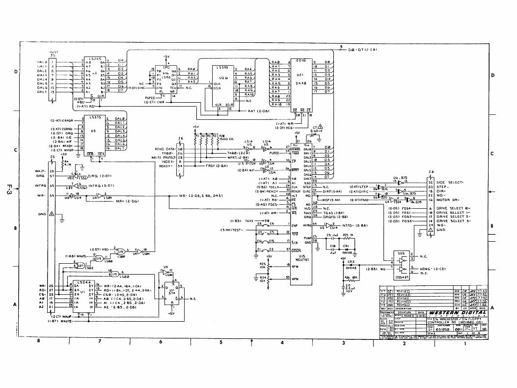
0
c
B
A
OAl :z IJAI I
DAl 2 OAl ~ OAL 4 OAL 5 OAl r. DAL 1
W"IT
ORa
INTRQ
MR-
GND
WR
RO
es-AQJ
AI ,,2.
8
du::'T r-----. 012)-01 (Z-CII}
IS
't~ .-- l 0;.24 S I ---~ I\e 1:>1;
II D'li RAG! 8 ZOIC.
<:I 00
~ "1 S I IZ CI CPD L!!. ~9:' RAt 1 10 01
5 ---..... ~ :~ wZ Be. I~ 02
j P0 UIC. 00 :!. R ... " 3 RA4 RA2. <D II 02.
1 ----. W B!:o 14 03 2 RAI 4 RA5 RA~ 5 I'!. 03 rs PI L SI~3 Cli uz I 9 ----. A4 S4 15 04 1(1) '" RAl. U2.C# 5 RACo RA4 4 14- 04 ~ P2. Ol 1\ "3
IB IlD 05 NC 9 1 RA3 I IClK
W RA1 RAS. 3 2KX8 15 OS p~ 03 I:!. 3
A2 B2 11 oc. (2·01) CINC.---? CPU TCU p.!L N.C. ~ ZClK \I RAB RAiD 2 Ie. DiD
15 2 AI BI Ie. 07 PL MR 10 RMI RA1 I 11 01 r; DIR PUP2Z-.J11 114
9 RAI0 RA8 23
4- t2.·~~~_-119 11 (Z-C1) CMR ~ r-N.C. RA':I 22
(I-All RO- (CUI zelR RAI0 1':1
I Iz liZ
RA1 (2·06) or VilIT I I
{;!J" (2-"1IERRQR~ l':.313 2 OAl0
.-2 C. OAL I (I-All WR-
l'2.·"11 caRRO -~ 5 OALZ ~SV (Z-011 Res- Cl & (Z·011 Of\a-~ U3 ':I OAL3 t5V
5·e.O pf
(Z-B4} SC!-~ IZ. OAl4 RI R21 RZ R.3 t R20 t~1 15 oALS
r6 Isan EA. 12-B4} WF -~ + LSl4 l SI4- 2r. -=
(2-B41 REAQV-~ Ie. DALe. 9~S6 U5 V" VLO
(Z-Ol W"UP-~ 19 OAL 1 RE"O OATA- 30 5r.:, C. 21
RAWRD Dlll0 ~ 00
H00-tZ.C!f) v pupzz-~ 01 ISJ' -= 5£B OEA TK00- zr. fii'i0 DAli
II rll WRITE PROTECT- za WPRT-(Z-~~) 10 .3 4 _~ DIIlZ 9 OZ
r+ ~j" INoEX- a ~ fl5 DI\l3 10 03
REAOY- 34 FROY (Z-B4-) OAl4 II 04-
2':1 -= lZ·B4) WF 13~S 12- 3IoWPl!T OAL5 1'2. 05
I 4- v L!>14 I~ DC. r+ S :"'3G.10RQ. (2-0"1) OAL" 31
(1- ... 1) A0~ 14 01 U2'2 A0 OAll uu" !!O':)
II-All AI-..! 25 13 ... IZ
3S UZ; ~Le.S3"1'NTRa (2.-011 AI $SO
(Z-1I11!:.TEP~ ,... :!.Z
C3-B5) FQCLK-~ Cl ... STEP ~N.C. 20 (Z-a4) READY ~ READY OIRC ~OIRF'C~-A4) • uc. :!> ... 4
16
3,':1 f------£0~LI:14 r u~~ MR- (Z-Da,2. e.o, 2+.31 N.C.~ HLT WO 31 IZ·fllIDIRC II ... 1121 ,... UI.o,SOS
22
r (I-All RO--~ Ii! _LWOFI ?·A4) (Z-A1)FMc)-
Uc.~05.3i", .. 9 ..... a ICo MR+ (2-OC.l U4 1.:'04 "u£'.505 C1. ~0
(2.-AS) FOC$--~ WG MR HlO t#-N.C. (Z-OS) FO$4--- ta
& f-""J.
(i-All WR--~ WE TGB ~ TG4!1 (I-B4-1 (Z-OS) FOS.I-- 10
ORG ~ ORQFO (Z-&&) IZ-OSI FoS,Z-- 12 CI-B~I TG4~ --ofll2l
~INTFD- (2.-B8)
(Z-051 FO~:.3.-- 14 E~ E9 I ENP INTRQ .--- Z4
(~-A4ITE5.T-
~- E~ 1 2Z ffiT' r& PUMP 2';,
C9 .I.J RZ., I ... -= q:. ~E15 11 SIb GND ri 1 CI0 I eRI 1 (Z-01) HSC- 2
? II ..... 1121 ~E2 31 OOEN I ut,\ J ... r IN41411 J:. .----12 U4 L':.04 U2S
~I- N.C. C,·-",&l W/lUPz. II L':.00 =- +Sv UIS
~ 13 U9 l~0121
'NO 2.191 +5V ~-Z I CRZ f.=
DU21 LS02. R2S III RPW
4-
U~ la~
6J WG-.2 ~ ~I-lOWG-( 10
~ (Z-B~)
91u9 B
l!'.04 ~ I-=-- N.C.
~ ''"' :13 WPW R3£o 10 ... 053.461
'" L!>244 ICo 4 - 10K '--
zst-t- 2A 2Y!-=-WR-/2-A4,!-I!.4,I-C41 ~D SG~ _ell Zlt-t- 11 2."UI z.Y~ RO-II·B4.1-01,2.·A4,z·oa, 1 2•2 .... UII 10'1 V 5Z1 I:£VI:.£.D 23.t-~ ZAo ZY~CS0- (2-115,Z-0&) 5101- IV 1 RE.VI~E.O
I1I----f,; IA IV~ ... 0 (I-C4.2-BS.Z-O&) ,-~p Q~ I-N.C. v5 4'3 lilVISLO
19 ~ IA IV ~ AI (l-e4 2.-1!>5 Z-Oa) R Y.<l ·90 Rlvl:;EO
2.1 ~ IA IY ~ A2. ~Z.B5. Z.Dal I Y3 re REVISED
~Z.Cl1 WAUP
"EV EeD DESCAU':TIOH
rl':l YI +SV rr:-~~~moE) SIGNATURE OATE W " .. ··i.~RIARTE .·IU~
II-Bl) WAU~ 1 xx t 010 CHICII. "'""55
SIDE SEL!:CT
$TEP_
OIR-WD-
MOTOR ON-
DRIVE. SHEer 0-DR 1'1£ SELECT 1-DRIV!: $E lECT 'Z
DRIVE ~E.LECT :!>WG-
GND
MH cc;: 11'1/1 ce 1"1/1 MH coO II.1H e.c:
r-----~7------~----~6------~----~5~-----r------~4------.-------l------~~~~~2~~~~~~~~==~
o
c
B
A
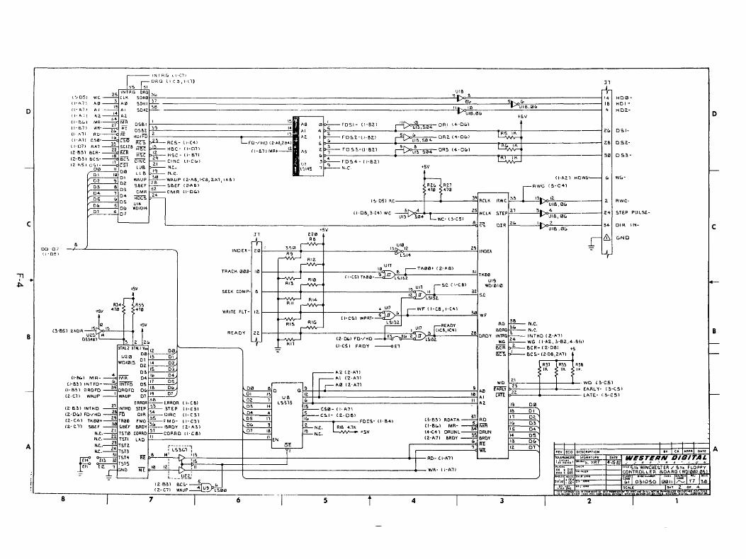
D
c
" '-~
B
A
00-07 r:.1·D~ 'I
~INIH.(:'L'-C'11
,-DRO \1(::',1-<-,) '>5 131
2S INTRQ ORa ~~ UI8 (~- D51 we ~ (l'" ~OHI2I~----------------------------------------------.2...J~ l>o~ (I- All 1'.0 ~ 1'.0 5DHI ~ ------------------------------------------....:.2~----....:5'_1l>ou~e."Go 11-1'.11 AI ~ AI SOHLF "l>o~I~,ej(. (11'::,1)) A2--H 1lo2. I I"
,~~ MR-~ MR OSBI -----------------------=-•• 11121 II-B'I wP,---f/:!!!- OSB2. ~q 14 AI (I- 1\,1 RO-~ RE HO/fO I, A2.
(I-II,) C5121-~ ~ RCS ~ Res- Ll-(4) L FO -/ HD (Z-"8,204 )
(I-Dl) RA' --t2 SCI2!!> ,:re;c bJ2-- HBC- (1-0,1 (I-Bl) MRt~ (Z-E'>31 E'>CR- -----i1 ~ Ho;.C ~ HSC - (I- B'1 {2.-E'>~1 eC5-~ BC~ CiNe f-7--- CINe lI-CC.l 12.1'.51 CSI:---< ESi LUB _21_ N_C._
~~ II~ DC/l LlB ~ N.C_
02 9 ~~ WAUP ~WAUP (Z-IIB,'~6,2.P.l,IA6) 03 8 SBEF -- SI!.EF" (Z-1I6)
D4 1 D3 CMR ~CMFI (I-D"')
OS CD ~~ HOCS ~
U7 l~145
--Ll.f"'- 10 1 V UI~,:;"'4 DFlI l4--Dc,,)
~DR2.{4-0c,,) ~ ~ U~~ 504 DR'!> (4--Dr.)
.5V
iFlWC
R~C ~~ I~::: ~~c. R~l 470 ~70
(~- OS) I'.C _____ --f __ ~-----'3'_1q RCLK
r+ 14
16 4
2c.
26
:!.0
(I-AZl HDWG-- Go
1~-C41
12. UIB,I2lc.
2.
Dr. 5 DC. ~~iOI4 01 4 01 LI-DB,~-(4) WC .3
UI~
Xl-4~ ______ -=l=l5 WCLII 5 TEPI-'2.o..:l __ ---=3"11 ..... 1,:O..c:,..,.--= _____ ~
51214 Lwc- (3-C5)
4 24 UIB, 1IlC.
, ________________________________________________________________________ ~8 ~
iSV
2. 34 UII!., elC"
OlRr2~r.=------I~~~Do~~~------~
31 Z20 rt- RB 3~QJ ~ 1,_UI01~ Z~
INOEX- l01----~-=;R:,:;n,.=--...... 1----.+---------...:.,~"Ji')c .... ,:.!<.=----------.::.~ lI'Ion ., I/'LSI4
~ TRIICK 011l12l- 11111---+---';'--_ --f ________ ..:,;10~U::_..,11 B ,--TK012l+ (2-IIB)
I .. T (1-C.5) H0121- 9 J ..a>)-l=-S,-F/ .. 2.----------=-=-l311 1\0121 ~ RIO ----<L-.../I UI9
1'.13 ~ r 1 - - - un soc (I-C8) 'toI010 I 121
SEEK COMP- II 1----+----~----I~-------------;lf~5li0:!I~1 ~----...:3~2 sc. ~ FlI4 ~L51!2.
15V
r &
l+
IU~ R3S
HOQl-HOI-
H02.-
09.1-
D5.2-
05.3-
YVG-
FlWC-
STEP PULSE.-
DIR 11'1-
GNO
("!I-B5) HDR,~,: " ". "":f.V uz.o:. 14
D5!.481 ~ 2. 2.t.
FlII~ WRITE FLT- 12.1---+---+---+----------;:4~UI;;-,,7 t. r WF (I-CB,I-C4) 3121 WF"
~ (1-(0:.) WPRT_~>-=-H>----------=l RI5 ~~_ ~LSI"!l2 REIIDY
I ... I un ~a fe41 Z2.I----+---...... -----------~~~~~~~~~lL~ ,
+ ~ (2-Dt.)F"0-/HO~L51~2. -=- 1'.11 (1-1:5) FRDY --OEl
READY zr. DROY
RG ~ N_C_ BaAa~ N.C_ INTRQ~ INTHD (2.-1111
~ ~~G (1-1\2.,:!o-B2.,4-IHil
lTIIL2 HH.I v .. 12 01211'----------...
U2121 ~~ I~ 01 WDIIOIIS 02. 14 02.
O~ 15 O? ~ "'2 (2.-Al) (HI(,,) MR-~ MR 04 lID 04 r- "'I (2-Al)
(I-B31 INTFD-~ INTrD DS:~ ~~ I'..::D,:;"=__ __ !:!.JII 0 I J M!l 12.-1\11
CI-B~l ORaPD ~ DRam OGo Q'-'91~+-4'_--------------_-------...:;14~~ AI\01 (Z-C1I WIIUP ---..!.. WAUP D1 l'l 01 Ol'~ r I ...
EAROA~ERROR (I-CB) 02. 1 L5U~~3 t-:Go~ ....... -----------------------....!I.!...il Al 2. E'>:!>l INTHD ---4. INTI-IO 5TEP ~ :"TEP (I-C3) D~ 14 ~ CS"- (I- All
(Z-Oc.) ro-/HD ~ fO DIR ~()IRC [I-C31 04 4 ~C!>I- (2.-0111
(~~~~; ~~~~+=1f ~~E~ ~~O~~1~~~~ ~~~~;\ ~~ I~ ~N_C_ T RI6 4_1K FOeS- (I-B41 ~~:~~~ R~:~~ ~ N,C--n 15T0 CORRDi=--CQRRO (I-Ca) 16 ~N.C_ L..Nv-- "S'{ 14-c.41 DRUNL~ ORUN N.C_~ TST! LIIO t-I..;...I - ____________ -+ ____ !.!..I" EN (2.-11.7) BROY ---== BRDY
BCR P=-BCR-C2-DB) +S ~ p.!- BC!)- (Z-06,2All
R~1 11'1
R~?> IK
R~I! I ~.
WD I-~=-=I,--_-_--+--+-~-- WD (~-·C5) rMU:V :~ , EARL Y- (!o-C 51 LIITE -LATE- t::!.-CS)
I~ Dill IB DI 11 02. I",
15 04 05
13 Dr.
D
c
B
N.r:._----P TST2. 1Sl: Go IfE" 1lC_-¥1 TST3 6 IJL~~C.;-:I~ I' ll.---------....:':..qwt 12 0, ---------4--~~~~-~A
~14 ~T~ ~~--~:~~~~I~ls~-----~-----~I-------------------~~l-~(I~) ~--~
WO 'tiM T515 10 12.: , II T _::- - r'- GNO WE ""R- (I-A"
~ L ___ h1~.~J (2·B3) e.cs- 5 r. (2.-C'1 WAUP -4 U<;I L500
8 7 6

D
c
"T1 ,-(1J
B
A
~N~-PlAN£ A· -- --e-'9-c.~r-\----1
I '~V :
: '" -=-~ I
I VCQ IN~_~_K4-___ lZ~K-6 ___ ~ I
(!> M ~.1!>3) I
I I I R~0 R4Z I
L_~"7 '" __ ,_"r ______ ~
I~t--~::~~
I
: R~2. II ~~0
~~~ ~ C21 22 p, I
I
1'.;\0 2111
I Clipl I
I ...... _ ........ __ ...... _--.J I
L~ _____ ~
RC (2·C4)
RC- (~'A41
(Z.·BZ.)E"RLY-
(2·B21lATE.-
13
r------+-+-Z.XDR (2BII)
EI'l
-SOV
191. QA 5
uz.~ GB i GC GO 12
FDelll (I·C4)
N.C.
N.C.
5.IDE.1 ~." '''.'''''"T _ B GNO (50LDER SIDE 1
D
00 I~ WC (Z.-C41
GI 1 'NDATA (4 ·em Q2'2 Q~ 10
WPCD (~·A41 ]"3
I INA
1 IND J2. r------------, 101 U~2. 1 c
UI~ l!>04
(2.C~)RWC~ ~: 51.4 :
r--+-r-~4-J I
(4·1!>C. DLYIN
(~·CC.1 V~O OUT (~. OBI Voo IN (4·C31 ORUN-
(3·CZ. WPCO· (3·B31 RDATA (3·051 RC-( I·B31 TG4~
(I·BS) TE5.T-(I. C31 DIRF" (I. B3) WOF
c.~~~ T"l. IN T2 ...
OUT T~ 10 T5
TEST eONNE£"OR
J9 ~
5
1 9 II
13
I 1 I
)O-;:-=t.---4O-'I-=-!~ I N B
1 1 ! N.C.
I I
, I
Q INC
L ____________ J E
t5V
RZt. Z20fi
12 .
+ OUTS
, OUle.
E
...
14
13
" N.C. 10
N.C.
JI
- MfMWD ~ MfMWD
B
~R~EV~EC~O~~DE~S=CR~"=TI=OH~---------~~~~~~~I A ERANeES SIGNATURE
(A~·~t~!lIj DfI''III~ '7,1RlAATE DATE
;·3(H
xx t 010 ,,=~--+---l xxx'!. 005 f"(',I"UII
8 r-· --~7'-----~----~6----~------~5------·t----~4~-----~----~3-----,-D~~~2~~~~~~~~~

c:
El
--------------~-------------------------------------------
MfMRD •
8
JI
QUTC ~ INC
J2.. OUTB 5
OUTA II r...
INB aUTO 13 N.c.
U!>CO 1----::-:-:-:-===--__ cI0::, 2r.. L S.~2
~~-----.9~ IN~
IZ.
(204) ORI
C2l 106Ft
14 15
12 e. RXl U ;SX2.Q
10 RDI (4-(1
i--------l tSV +SY
R5~ 220n
CR+
I I
L ____ _ GND PLANEC, ~
+~V I , DLYIN(~B41
R I!)
CR" ,...C_R-j& .. 1"'_4_14.6 __ ... ~~~ K I'
(~-Cl.)V,oaUT
7
(~·B~) ROATA
tSY
RI'l II'.
U~4
514
R Q
tSV
RSS II'.
R52. zzon
IN41H
CRS
11'14148
C!)I 1. .I ... ~ -=- I
~~ __ ~~~ I
c~z I .1 ... '
00 I
-=- ' c'.t>0 RS4- I
12 D Qr<:l=-+ __ -+-'--..... _C .. RI-~ ____ • __ -_----I .--~>--III--+E:.::Z~S .~ Y,o IN I
U34- L - C2S ,~- D&) I -=- 5.1+ 11'14148 3~.r
\~Cip.=.+---.J _____________________________ ~ PUPS0 -~----'
6
DR UN- (~rA+1
NQTE~:&J6 tTl GND PINS.: 1.:!.;1.<:I,".I~.IS)1,I~,l.1,2',2,5, 2.1,2.<:I,~1, '!>3, ,
£.:I5 COND PIN5.: 2.·4C21CEVEN PINONLV)
3 . .:II J2 J~ "NO PIN~: Z.4,C..S.IIII2..1511t..I~,Za. 4, I'\LL RES,ISTEP. VALUE.S, ~RE IN OHMS.
UNLEo:.S, OTHERWISE SPECIFIED. 5, ADD .I ... ~ C~P FROM ALL I.e v,. TO GND. 0 &. J9 GND PINS: ~IIO,IZ.,I~,14115,1r... ft:::. C,",P 5/B PHY:'ICALLY CL05.~ TO CHIP.
PUP22. ----
REv ECO DESCAIPTICN
fRANCES SIGNATuFiE OATE
(At ·~t~~D O"A."~, YRII\RT£. • ·1- 8.}
..... E~ PIQ., ~ l''''11 AP'II
_o~ :gg~,"u" .... :;;,,-,-+---1
GND
GND
c
B
IV CK ",'''1 DATE A

APPENDIX G
BILL OF MATERIALS
(to be supplied)
G-1